1
Application Note 1 – v1.0.5 – July 2014 FLIM measurements using SPC2 FLIM measurements using SPC2
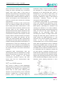
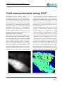
Fluorescence Lifetime IMaging (FLIM) is an imaging technique based on the differences in the exponential decay rate of the fluorescence from a fluorescent sample, rather than on the emission intensity [1]. The fluorescence lifetime of a molecule is a measurement of the emission decay-‐rate, which is a property of individual fluorophores, and thus it is unaffected by changes in probe concentration or excitation intensity. FLIM can be used for instance as an imaging technique in confocal microscopy and in two-‐photon excitation microscopy. FLIM images are most often obtained by employing the Time Correlated Single Photon Counting (TCSPC) technique and a point detector (such as a PMT). The latter is used in conjunction with an optical scanning system, in order to acquire the waveform histogram for each image pixel and reconstruct the entire image [2]. The exponential decay model is fitted for each pixel histogram in order to determine its lifetime. The intensity/color of each pixel represents the measured lifetime, giving the possibility to obtain images that present high contrast between materials with different decay rates, even if they fluoresce at the same wavelength, or, on the other hand, identify identical regions of the same material even if they emit with different intensity as shown by Figure 1. A typical application of FLIM is the study of Förster (or Fluorescence) Resonance Energy Transfer (FRET) [1]: a mechanism of energy transfer between two fluorophore molecules with the emission band of one of them overlapping the absorption band of the other. When this two components are in close proximity, the first one, called donor, initially in its electronic excited state may non-‐radiatively (without the emission of light) transfer the energy to the second one, called the acceptor. The result is the quenching of the donor fluorescence, thus the decrease of the donor emission lifetime. The efficiency of the energy transfer is inversely proportional to the sixth Figure 1: Example of living cell imaging with SPC2. Left: intensity image. Right: lifetime image. Note that the cell in background is barely visible in the intensity image, but clearly visible in the lifetime image [3]. AN1 -‐ 1 Application Note 1 – v1.0.5 – July 2014 FLIM measurements using SPC2 power of distance between donor and acceptor, making the effect noticeable only at distances shorter than 10 nm. FRET is thus used to determine the proximity in the nanometer range between proteins or other elements of interest associated with suitable fluorophores labeled as donors and acceptors. Such measurements are used as a research tool in fields such as biology and chemistry. Different ways of making a FRET measurement exist. The obvious problem with the intensity-‐
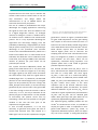
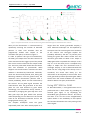
based steady-‐state FRET measurements is that the emission band of the donor extends into the emission band of the acceptor and the absorption band of the acceptor extends into the absorption band of the donor. Furthermore, the concentrations of donors and acceptors and the fraction of donor molecules linked to an acceptor molecule are variable and unknown. All this makes the intensity-‐based FRET measurements very difficult since they require a calibration with samples containing only donors and acceptors, or measurements in which the second step is the destruction of the acceptors by photo-‐bleaching. In this case, FRET measurements are obtained as the relative increase of the donor fluorescence intensity. FLIM-‐based FRET measurements have the advantage that results are obtained from a single lifetime measurement of the donor and are not affected by the changes in the sample concentration, excitation intensity and other factors that limit the intensity-‐based FRET measurements. breakdown voltage. Under this biasing condition, the absorption of a single photon causes the generation of an electron-‐hole pair, which is accelerated by the electric field across the junction. The energy of the charge carriers is eventually sufficient to trigger a self-‐sustained macroscopic avalanche current of few milliamperes through the device. A quenching circuit based on a time-‐varying active load (Variable-‐Load Quenching Circuit, VLQC) [5] has been integrated for sensing the SPAD ignition, quenching the avalanche and resetting the detector to its initial condition. Compared to quenching circuits based on passive loads, the VLQC has the major advantage of speeding up the quenching action, thus minimizing the amount of charge which flows through the SPAD after ignition. Moreover the VLQC controls the SPAD dead-‐time, i.e. the minimum time interval between two detection events. In case of FLIM measures, it is recommended to set it to the minimum possible value, which also guarantees a low or moderate afterpulsing probability (AP). Currently this value is equal to 200ns. Thanks to the integrated VLQC, the SPADs achieve moderate detection rates up to a saturation limit of 5 Mcps per second and per pixel without a significant decrease in the TCSPC dynamic range (low AP). The VLQC output, which is synchronous with the avalanche sensing, triggers the processing electronics and an 8-‐bit Linear-‐Feedback Shift-‐Register (LFSR) counts the detection events. Routing electronics is then SPC2 as a FLIM camera SPC2 camera is based on 1024 independent SPADs designed and produced in standard CMOS technology. The detectors are organized in a 32×32 array of smart pixels, featuring both detection and pre-‐processing of the measured photons. A SPAD [4] is a reverse biased p-‐n junction, which is operated well above its Figure 2: Front-‐end electronics inside each pixel of the SPC2, showing the gatable counter [5]. AN1 -‐ 2 Application Note 1 – v1.0.5 – July 2014 FLIM measurements using SPC2 implemented on the same chip to read-‐out the counter values and to transfer them to the off-‐
chip electronics. This design allows the measurements of up to 48’000 frames per second for the full array acquisition. The use of a SPAD as photodetector has major advantages for imaging applications concerning the signal-‐to-‐noise ratio. Since the detector acts as a digital Geiger-‐like counter, no analogue measure of voltage or current is needed. Hence, no read-‐out noise is added to the measurement process. This is a very important advantage for high-‐frame rate microscopy imaging, since the probability of detecting a single photon per frame and per pixel is usually low (<<1). A second major advantage of the presented pixel structure concerns the controllable dead-‐time, which has a lower limit of about 50 ns. In case the AP can be tolerated, the dead time can be reduced to such a low value, thus raising to 20Mc/s the maximum number of photons per pixel which can be processed per second. The in-‐pixel front-‐end additionally allows the gating of the LFSR counters for a very short time between 1.5 ns and 20 ns (Figure 2). In this way, the trigger signal by the VLQC circuit increments the LFSR counter only when the signal GATE is enabled (logic level ’1’). Otherwise, the detected photons are not counted (logic level ’0’). The gate signal can be provided by the user through the GATE_IN input of the camera, or can be internally generated by the camera itself. If the gate width is set short enough so that the counter is able to count only ‘1’ or ‘0’, not only a maximum of one photon per gate is acquired but it is also possible to time-‐stamp this photon arrival time by associating it with the time position of the gate window. In this case the time jitter of the acquisition is the gate width. In case of FLIM acquisitions, it is not only necessary to generate short gates but also to control with precision their shift respect to a SYNC signal. The circuit that implements the gate Figure 3: Circuit implemented inside the FPGA to generate the variable width/shift gate signal. generation is shown in Figure 3, and allows both for gate width adjustment and for gate shifting with respect to the internal reference clock. It is based on the internal Delay Locked Loops (DLLs) of the FPGA device that controls the SPC2 camera. FPGA devices require DLLs to de-‐skew the internal digital paths and to fine-‐tune the sampling time of fast serial communication lines. They are designed to produce a precise phase shift between 10 and 40 ps, which can be dynamically controlled during operation. This dynamic phase shift is well suited to generate periodic sequences of pulses. The internal 50 MHz clock (Int_Clk) is sent to DLL1, which halves the frequency and de-‐phases the clock of a delay ∆Φ1. This clock signal, Int_ClkD1, is then sent to a second DLL (DLL2), which creates an additional phase shifted clock (∆Φ2, Int_ClkD2). The XOR between Int_ClkD1 and Int_ClkD2 creates short pulses at the same repetition rate of the internal reference clock, with adjustable phase and duration. The phase difference between Int_Clk and Int_ClkD1 will be referred to as gate shift while the phase between Int_ClkD1 and Int_ClkD2 will be denoted gate width. Both gate shift and gate width can be dynamically adjusted during data acquisition. This advanced gating capability enables the use of SPC2 as a FLIM camera. In fact, it is possible to employ the gate in order to implement a time-‐
gated FLIM detection system [6], which, as opposed to PMT-‐based systems, does not require any scan of the sample. In time-‐gated FLIM the AN1 -‐ 3 Application Note 1 – v1.0.5 – July 2014 FLIM measurements using SPC2 Figure 4: Optical waveform reconstruction using the Gated-‐FLIM approach with the SPC2 camera. decay of the fluorescence is reconstructed by repetitively counting the number of detected photons in short time windows that are progressively shifted with respect to the excitation laser pulse, as shown in Figure 4. In order to perform this type of measurement, the SYNC_OUT output from the SPC2 camera has to be connected to the trigger input of the pulsed laser source used to illuminate the sample under test. The laser pulse width should also be shorter than few hundreds of picoseconds. What happens next is well known in literature: the laser radiation is absorbed by fluorescent molecules, which are electronically excited; then, during the following relaxation into the ground state, the molecules emit fluorescence photons with a certain probability, which are then measured by the camera. The Int_Gate signal activates the LFSR counters after the generation of the laser pulse for the time defined by gate width. Accordingly, the fluorescence decay kinetics is measured by changing the gate shift over time. Both gate shift and gate width have optimal values depending on the lifetime of the excited state of the fluorescent molecules and on the imaging frame-‐rate [7], [8]. The simplest techniques move the gates sequentially with their shifts exactly equal to or longer than the chosen gate-‐width. Anyway a more advanced technique can be exploited by the expert user for increasing the time-‐resolution of the camera. This technique exploits the possibility offered by the SPC2 of precisely time shifting the gates with values smaller than the minimum gate width of about 1.5ns: 100ps or 400ps gate-‐shifts are possible for example. In this way it is as if the decay curve is sampled every 200ps or 400ps but also convoluted with a rectangle. Anyway it can be demonstrated that while the fast rising edge of the decay curve is smoothed, the actual slow decay (i.e. the information to be acquired) is still accurate. Such small gate-‐shifts produce equivalent-‐gate widths shorter than the actual hardware one and thus allow for better time jitter performances. Using SPC2-‐SDK for FLIM As described above, a time-‐gated FLIM can be performed with a SPC2 either by providing an external gate signal, or by employing the embedded gate generation feature. Of course, the latter is for sure the more straightforward option thanks to the availability of two specific DLL functions devoted to the easily setting of the internal gate: AN1 -‐ 4 Application Note 1 – v1.0.5 – July 2014 FLIM measurements using SPC2 SPC2Return SPC2_Set_Gate_Mode(SPC2_H
spc2, GateMode Mode)
SPC2Return SPC2_Set_Gate_Values(SPC2_H
spc2, Int16 Shift, Int16 Length)
Enabling the SYNC_OUT in order to output the internal reference clock is also very simple using the specific function: SPC2Return
SPC2_Set_Trigger_Out_State(SPC2_H
spc2, TriggerMode Mode)
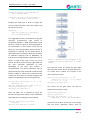
The suggested flow chart to follow for writing the necessary programming code aimed to successfully perform a FLIM measurement with the SPC2 is shown in Figure 5. The starting point is the initialization of the camera which can be done as in the example below, where the SPC2 is initialized by enabling the full 32x32 pixels in advanced mode, by setting a dead-‐time of 200ns, an hardware exposure time of 4096x20ns, an internal sum of 1000 hardware exposure times to obtain a single frame and a snap size of 10 frames. Of course actual settings might differ for the user’s particular application (a basic knowledge of the SPC2 user manual is recommended). The actual acquisition will be performed by the snap commands inside the loop shown in Figure 5, where every saved frame will contain, for every pixel, the TCSPC histogram bin height corresponding to a particular gate shift. out=(int)SPC2_Constr(&spc2, 1, 32, 1, 32,
Advanced, "");
SPC2_Set_Camera_Par(spc2, 4096, 1000,10);
SPC2_Set_DeadTime(spc2, 200);
SPC2_Apply_settings(spc2);
Then the SYNC out is enabled by using the function already shown above, and, immediately afterwards the internal gate is also enabled: SPC2_Set_Trigger_Out_State(spc2,
Gate_Clk)
SPC2_Set_Gate_Mode(spc2, Pulsed);
Figure 5: Flow-‐chart of the operastions to be performed in order to employ SPC2 as a FLIM camera. The loop then starts by setting the gate width and phase like below, where the gate signal has a 3 ns width and is shifted 2 ns respect to the internal reference clock: SPC2_Set_Gate_Values(spc2, 10, 15);
//Shift 10% of 20 ns --> 2 ns, Length
15% of 20 ns --> 3ns
SPC2_Apply_settings(spc2);
The counts for this gate value can then be acquired and saved as a snap: SPC2_Prepare_Snap(spc2);
SPC2_Get_Snap(spc2);
SPC2_Save_Img_Disk(spc2, 1, 10,
"SNAP_loop_1.spc2", SPC2_FILEFORMAT);
Of course one iteration of the loop is not enough and the three operations above must be AN1 -‐ 5 Application Note 1 – v1.0.5 – July 2014 FLIM measurements using SPC2 repeated for the desired number of shifts (gate width is never changed). When no more shifts are needed, the camera is closed. Now on the HDD are saved a series of files in SPC2 format acquired with the corresponding gate shift. These snaps can then be analysed in order to extract the desired information: i.e. for each pixel reconstruct the full decay histogram and then calculate the decay time constant. Since every snap can be composed by n>1 frames (in our example 10) it is recommended to average or sum all of them in one single frame. This can be done easily for example with ImageJ. A fast, powerful yet convenient way of analysing the MPD camera data is through the use of the PixBleach [9] plugin for ImageJ which allows to obtain a lifetime image once Snaps from SPC2 has been imported in ImageJ using the provided plugin. An accurate reading of ImageJ and PixBleach documentation is also recommended. The remaining parameter to take into account is that the SPC2 gate has a maximum shift range of 20 ns. This means that the SPC2 is equivalent to a TCSPC acquisition system with a 20 ns full scale range. Longer ranges might be achieved with a different technique that will be discussed in a future application note. Finally it worth noting that the SPC2 has already been used successfully to measure eGFP lifetimes of about 2 ns and that a peer reviewed paper has already been submitted. Gate calibration The actual width and phase of the gate signal obtained for a given set of parameters used with the SPC2_Set_Gate_Values function may vary among different SPC2 units, due to fabrication tolerances of the FPGA. While the gate width is calibrated by MPD before shipping the camera, the gate shift is not. This is done on purpose. In fact, the final shift of the gate signal with respect to the laser pulse is not only related to the shift internal to the camera, but also (and probably largely) to the delays introduced by cables and the laser itself. A calibration of the actual gate shift with respect to the laser excitation is therefore necessary after the camera is mounted into the measurement setup. This can be easily done by directly shining the laser onto the array, without interposing any fluorescent sample or filter, and performing a full measurement over the entire 20 ns shift range. By inspecting the measurement and finding the laser peak, it is possible to evaluate the shift between the actual laser pulse and the Int_Clk signal. Once this shift is known, it is advisable to adjust the length of the cable from the SYNC_OUT SMA output of the camera to the TRIG_IN of the laser in order to “centre” the fluorescence in the 20 ns FLIM window. This would avoid any folding of the fluorescence signal, avoiding at the same time the initial and final part of the FLIM window that presents poorer linearity. The calibration is also useful to zero any skew among pixels. In fact the gate applied to each pixel of the camera has a small skew compared to any other pixel. These relative skews are small and totally negligible in case of a FLIM acquisition, where the relevant information is constituted by decay times; anyway they might not be negligible in other cases like 3D indirect time of flight measurements in which the absolute delay IS the measure itself. The evaluation of actual gate width after calibration is possible by comparing photon counts obtained with and without the gating function, when the camera is illuminated with a constant light source. In this way it is also possible to check the gate width constancy against different gate shift values. An example code for this aim is the following: //SPC2 constructor and parameter setting
out=(int)SPC2_Constr(&spc2,1,32,1,32,
Advanced,"");
AN1 -‐ 6 Application Note 1 – v1.0.5 – July 2014 FLIM measurements using SPC2 SPC2_Set_Camera_Par(spc2, 1024*1,
10000,2);
SPC2_Set_DeadTime(spc2, 400);
SPC2_Apply_settings(spc2);
printf("Expose the SPC2 camera to a timeindependent luminous signal\n(be
careful! room light might oscillate
at 50 or 60 Hz and should be
avoided)\nPress ENTER to continue
...\n");
getchar();
if((f = fopen("GateValues.txt","w")) ==
NULL)
{
printf("Unable to open the output
file.\n");
break;
}
//photon counts without any gate
SPC2_Set_Gate_Mode(spc2, Continuous);
SPC2_Apply_settings(spc2);
SPC2_Prepare_Snap(spc2);
SPC2_Get_Snap(spc2);
SPC2_Average_Img(spc2, data);
gateoff = mean_double(data,1024);
printf("Gate OFF counts:
%.2f\n",gateoff);
fprintf(f,"Gate OFF counts:
%.2f\n",gateoff);
SPC2_Set_Gate_Mode(spc2, Pulsed);
printf("Acquiring:\n\nGate\t\tMean\t\tAct
ual Gate\t\t\n");
//photon counts for gate witdh ranging
from 0% to 100%
for(i=0;i<=100;i+=1)
{
SPC2_Set_Gate_Values(spc2, 0, i);
SPC2_Apply_settings(spc2);
SPC2_Prepare_Snap(spc2);
SPC2_Get_Snap(spc2);
SPC2_Average_Img(spc2, data);
y[i] = mean_double(data,1024);
y[i+101] = y[i]/gateoff*100; //actual
gate width calculated from photon
counts
x[i]=(double) i;
printf("%3.0f\t\t%.2f\t\t%.2f\n",x[i],y[i
],y[i+101]);
fprintf(f,"%.0f %.2f
%.2f\n",x[i],y[i],y[i+101]);
}
fclose(f);
printf("\n");
References 1.
2.
3.
4.
5.
6.
7.
8.
9.
Joseph R. Lakowicz, Principles of Fluorescence Spectroscopy 3rd edition, Springer (2006). J. Pawley, Handbook of Biological Confocal Microscopy, 3rd Edition. New York: Plenum Press, 2006. M. Vitali, D. Bronzi, A. J. Krmpot, S. Nikolic ́, F. Schmitt, C. Junghans, S. Tisa, T. Friedrich, V. Vukojevic ́, L. Terenius, F. Zappa, Senior Fellow, IEEE and R. Rigler “A single-‐photon avalanche camera for fluorescence lifetime imaging microscopy and correlation spectroscopy”, JSTQE, 2014. S. Cova, M. Ghioni, A. Lacaita, C. Samori, and F. Zappa, “Avalanche photodiodes and quenching circuits for single-‐
photon detection.” Appl Opt, vol. 35, no. 12, pp. 1956–1976, 1996. S. Tisa, F. Guerrieri, and F. Zappa, “Variable-‐load quenching circuit for single-‐photon avalanche diodes.” Opt Express, vol. 16, no. 3, pp. 2232–2244, 2008. T. W. J. Gadella, Ed., FRET and FLIM Techniques, Volume 33. Amsterdam: Elsevier Science, 2008. S. P. Chan, Z. J. Fuller, J. N. Demas, and B. A. DeGraff, “Optimized gating scheme for rapid lifetime determinations of single-‐exponential luminescence lifetimes.” Anal Chem, vol. 73, no. 18, pp. 4486–4490, 2001. D. D.-‐U. Li, S. Ameer-‐Beg, J. Arlt, D. Tyndall, R. Walker, D. R. Matthews, V. Visitkul, J. Richardson, and R. K. Henderson, “Time-‐domain fluorescence lifetime imaging techniques suitable for solid-‐state imaging sensor arrays.” Sensors, vol. 12, no. 5, pp. 5650–5669, 2012. http://bigwww.epfl.ch/algorithms/pixbleach/ Copyright and disclaimer No part of this document, including the products and software described in it, may be reproduced, transmitted, transcribed, stored in a retrieval system, or translated into any language in any form or by any means, except for the documentation kept by the purchaser for backup purposes, without the express written permission of Micro Photon Devices S.r.l.. All trademarks mentioned herein are property of their respective companies. Micro Photon Devices S.r.l. reserves the right to modify or change the design and the specifications the products described in this document without notice. Contact For further assistance and information please write to imaging@micro-‐photon-‐devices.com. AN1 -‐ 7