1
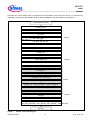
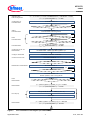
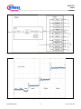
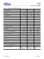
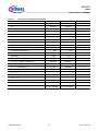
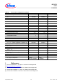
Tri Cor e AP 3217 8 cstart Applic atio n N ote V1.0 2011-08 Mic rocon t rolle rs Edition 2011-08 Published by Infineon Technologies AG 81726 Munich, Germany © 2011 Infineon Technologies AG All Rights Reserved. LEGAL DISCLAIMER THE INFORMATION GIVEN IN THIS APPLICATION NOTE IS GIVEN AS A HINT FOR THE IMPLEMENTATION OF THE INFINEON TECHNOLOGIES COMPONENT ONLY AND SHALL NOT BE REGARDED AS ANY DESCRIPTION OR WARRANTY OF A CERTAIN FUNCTIONALITY, CONDITION OR QUALITY OF THE INFINEON TECHNOLOGIES COMPONENT. THE RECIPIENT OF THIS APPLICATION NOTE MUST VERIFY ANY FUNCTION DESCRIBED HEREIN IN THE REAL APPLICATION. INFINEON TECHNOLOGIES HEREBY DISCLAIMS ANY AND ALL WARRANTIES AND LIABILITIES OF ANY KIND (INCLUDING WITHOUT LIMITATION WARRANTIES OF NON-INFRINGEMENT OF INTELLECTUAL PROPERTY RIGHTS OF ANY THIRD PARTY) WITH RESPECT TO ANY AND ALL INFORMATION GIVEN IN THIS APPLICATION NOTE. Information For further information on technology, delivery terms and conditions and prices, please contact the nearest Infineon Technologies Office (www.infineon.com). Warnings Due to technical requirements, components may contain dangerous substances. For information on the types in question, please contact the nearest Infineon Technologies Office. Infineon Technologies components may be used in life-support devices or systems only with the express written approval of Infineon Technologies, if a failure of such components can reasonably be expected to cause the failure of that life-support device or system or to affect the safety or effectiveness of that device or system. Life support devices or systems are intended to be implanted in the human body or to support and/or maintain and sustain and/or protect human life. If they fail, it is reasonable to assume that the health of the user or other persons may be endangered. AP32178 cstart TriCore Revision History: V1.0, 2011-08 Martin Schrape Previous Version: none Page Subjects (major changes since last revision) We Listen to Your Comments Is there any information in this document that you feel is wrong, unclear or missing? Your feedback will help us to continuously improve the quality of this document. Please send your proposal (including a reference to this document) to: [email protected] Application Note 3 V1.0, 2011-08 AP32178 cstart Table of Contents Table of Contents 1 Preface ................................................................................................................................................ 5 2 Introduction ........................................................................................................................................ 5 3 Overview ............................................................................................................................................. 5 4 Implementation and Usage ............................................................................................................... 9 Application Note 4 V1.0, 2011-08 AP32178 cstart Preface 1 Preface This application note describes a user’s startup code implementation on the TriCore processor architecture [1,2] for the AUDO MAX-family. The document is aimed at developers who write or design applications for the TriCore. This application note assumes that readers have access to the TriCore Architecture Manual [1] and TriCore User Manual [3-6], and have at least some knowledge about the following sections of the user’s manual: Startup SoftWare (SSW) (see section BootROM content in [3-5]) Clock system of the System Control Unit (SCU) (see section Clock System overview in [3-5] ) ENDINIT protection and watchdog timer (WDT) (see section Watchdog Timer in [3-5]) The TriCore instruction set. See References on Page 13 for more information on the TriCore manuals and other relevant documentation. 2 Introduction Compilers for the TriCore processor are available by third party Infineon tool partners and offers user’s startup code with their tool chain. It is provided as C source code or assembler source code. The source file for the user’s startup code named cstart.c for Tasking, crt0.S for Hightec and crt0.s for Wind River. This application note is written explicitly for Tasking users. It improves and extends the default Tasking startup file cstart.c in four ways. First it improves the PLL initialization and implements a program flow exactly as described in the user’ manual. Second it extends the number of registers that could be configured in the startup code. It especially offers configuration for most ENDINIT protected registers. ENDINIT bit protected register are typically needs to be configured only once at startup. Grouping them together makes it possible to clear and set the ENDINIT bit only once. This practice saves execution time which is often critical at startup. An endinit_clear()/endinit_set() programming sequence typically requires about 0.5 µs running at 180 MHz CPU frequency. Third a fast ENDINIT bit clear and set routines are offered as inline functions. Fourth the cstart.h header files comes with PLL initialization values for most popular configurations of the TriCore AUDO-MAX family. To limit the jump of the dynamic current consumption the PLL initialization uses a ramp-up sequence. Together these modifications of the default Tasking startup code give the user a quick start programming the TriCore. With entering the C main() function the processor is already running at the configured CPU frequency and configured modules frequencies. 3 Overview The PLL uses two different start-up mechanisms depending on the triggering reset. Upon a power-on reset the PLL starts to supply the system in Precscaler Mode. The starting frequency is 16.6 MHz. A system reset brings the PLL control register in the SCU to the defined reset values and the system clock operates in free-running mode at fVCOBASE/16. In both cases the SSW in the BootROM restores the clock system to free-runnning mode before jumping to the user’s startup code located at the User STartup ADDress STADD. Tasking named this address the RESET vector. Two addresses are valid: 0xA0000000 for starting from internal flash memory module (internal start) or 0xA1000000 for starting from external EBU space (external start). The SSW therefore evaluates the HWCFG[7..0] pins. For external start the EBU reads its configuration parameter from internal memory 000004H (see section External Bus Unit in [7], chapter ‘Boot Process’ respectively ‘Configuration Word Fetch Process’). The major design goal of the user’s startup code is to initialize the processor and to bring up the PLL quickly, to configure major CSFR and other ENDINIT protected SFR registers. The steps are illustrated in Figure 1. The changes made to the original code are mainly related to the PLL ramp-up sequence and the ability to configure more ENDINIT protected sfr registers. The execution time on a TC1798 running at 300 MHz CPU frequency of the startup code is about 250-350 µs, where the largest single part (230 µs) is the ramp-up sequence using six steps with a delay in between two steps of 20 µs. Details of the PLL ramp-up sequence are illustrated in Figure 2. A block diagram of the Clock Generation Unit (CGU) is shown in Figure 3. The current consumption during a PLL ramp-up sequence with just four steps is shown in Figure 4. Formulas for the dynamic current consumption are given in the data sheet. The internal Watchdog starts after reset in Time-Out Mode. With the startup code presented by this application node the watchdog would enter Prewarning Mode after 4 × fFPI/16384 which is measured to 950 µs. The Application Note 5 V1.0, 2011-08 AP32178 cstart Overview execution time of the startup code as configured in this application note is less than 300 µs. To safe time the watchdog is serviced and the ENDINIT bit is set after all ENDINIT protected registers are configured. Start at address STADD Init Stack pointer Init PSW Init PCXI Init WDT deleted Init BTW, BIV, ICR, ISP Init PMU/PMI Init DMI Init EBU_CLC Init OSCCON Init PLL Ramp-Up modif ied Init SCU FDR Init DTS Init STM_CLC Init PCP_CLC, PCP_CS Init GPTA0_CLC, GPTA_FDR Init CAN_CLC added Init ADC_CLC, ADCn_GLOBCFG, ADCn_GLOBSTR Init SSC0_CLC, SSC0_FDR Init DMA_ME0AENR, DMA_ME0ARR modif ied Init WDT Init CSA, FCX Init EBU_CON, EBU_ADDRSELn, EBU_BFCON, EBU_BUS APn, EBU_BUSCONn, EBU_EMUAS, EBU_EMUBAP, EBU_EMUCON Call main Figure 1 Startup code Flow Diagram Application Note 6 V1.0, 2011-08 AP32178 cstart Overview SSW exits with Free-running Mode Conf igure K1 f or Prescaler Mode f PLL = fVCOBase/K2 = fPLLBase/K2 = 200 MHz/(K1DIV+1) = 200 MHz/16 = 12 MHz fCPU = f PLL/(CCUCON.SRID IV+1) = 12 MHz PLLCON1.K1DIV = 0 yes PLLSTAT.K1RDY== 0 Select Prescaler Mode PLLCON0.VCOBYP = 1 Prescaler Mode; VCO is bypassed yes PLLSTAT.VCOBYST==0 Enter Prescaler Mode yes OSCCON.PLLLV==0 Prescaler Mode fPLL = fOSC /(K1DIV+1) = 20 MHz/1 = 20 MHz fCPU = f PLL/(CCUCON.SRID IV+1) = 20 MHz Conf igure N, P, K2 f or Normal Mode PLLCON0 = __SCU_PLLCON0_VALUE PLLCON1.K2DIV = (NDIV+1)*(K1DIV+1)/(PDIV+1)-1 Conf igure CCUCONn CCUCON0, CCUCON1, CCUCON2 Connect clock to VCO PLLCON0.CLRFIND IS = 1 yes PLLSTAT.FINDIS == 1 Restart VCO Lock Detection PLLCON0.RESLD = 1 yes PLLSTAT.VCOLOCK == 0 PLLCON0.VCOBYP = 0 Normal operation; VCO is not bypassed yes Enter Normal Mode Normal Mode PLLSTAT.VCOBYST==1 fPLL = (NDIV+1)/(PDIV+1) /(K2DIV_0+1) fOSC = 20 MHz fCPU = f PLL/(CCUCON.SRID IV+1) = 10 MHz SCU_PLLCON1.B.K2DIV = K2DIV_n (n=1…6) PLL ramp-up Wait 20µs Normal Mode Figure 2 fPLL = (NDIV+1)/(PDIV+1) /(K2DIV_6+1) f OSC = 600 MHz fCPU = fPLL /(CCUCON.SRIDIV+1)= 300 MHz PLL initialization Flow Diagram (TC1798 300MHz) Application Note 7 V1.0, 2011-08 AP32178 cstart Overview Figure 3 CGU and CCU Figure 4 Current consumption during frequency Ramp-up sequence. Application Note 8 V1.0, 2011-08 AP32178 cstart Implementation and Usage 4 Implementation and Usage The implementation follows the default Tasking startup file cstart.c but modifies or adds certain parts as explained in section 3. The cstart.c and cstart.h files that come with this application notes replaces the Tasking C startup files The new cstart.h header file offers popular configurations for the AUDO-MAX TriBoards. TC172x 80/132 MHz TC178x 132/180 MHz TC179x 240/270/300 MHz To enable one of these configuration the control program cctc should be called with option __<TriCore Derivative>__ and __fCPU=<frequency[MHz]>, for example –D__TC1798__ -D__fCPU=300. Select Project > Properties and navigate to C/++ Build > Settings > C/C++ Compiler > Preprocessing and add these symbols to the list of defined symbols (Figure 5). These macros will select the appropriate settings in cstart.h. Listing 1 shows this configuration for the TC1798 running at 300MHz. More changes to the cstart.h are also reflected by more options in the cstart editor within the Tasking EDE. Figure 6 for example shows the register page with ADC, CAN, GPTA, SCU, SSC and STM registers. Details of the configurations are listed in Table 1 to Table 3. Figure 5 239 240 241 242 Add Preprocessor symbols #elif (defined __TC1798__ #if __fCPU==300 // fPLL=600MHz // fPCP=200MHz Application Note || defined __TC1793__ || defined __TC1791__) 9 V1.0, 2011-08 AP32178 cstart Implementation and Usage 244 245 246 247 248 249 250 251 252 253 254 255 256 257 258 259 260 261 262 263 264 265 266 267 268 269 270 271 // fFSI=150MHz // fSRI=300MHz // fFPI=100MHz // fEDBBB=150MHz // fREFCLK=25MHz // fMCDS=150MHz // fEBU=75MHz // fERAY=300MHz // fOUT=25MHz #define __SCU_PLLCON0_INIT #define __SCU_PLLCON0_VALUE #define __SCU_PLLCON1_INIT #define __SCU_PLLCON1_VALUE #define __SCU_PLLK2RAMPUP_INIT #define __SCU_PLLK2RAMPUP_VALUE #define __SCU_PLLK2RAMPUP_WAIT #define __SCU_CCUCON0_INIT #define __SCU_CCUCON0_VALUE #define __SCU_CCUCON1_INIT #define __SCU_CCUCON1_VALUE #define __SCU_CCUCON2_INIT #define __SCU_CCUCON2_VALUE #define __SCU_FDR_INIT #define __SCU_FDR_VALUE #define __FLASH0_FCON_INIT #define __FLASH0_FCON_VALUE #define __FLASH1_FCON_INIT #define __FLASH1_FCON_VALUE 1 0x1017600 1 0x0 1 0x08040201 6000 1 0x2030105 1 0x30B03 1 0x701 1 0x43FE 1 0x00074804 1 0x00074804 Listing 1 PLL specific configuration in cstart.h. TC1798 with fCPU=300Mhz shown Figure 6 start editor: Register page Application Note 10 V1.0, 2011-08 AP32178 cstart Implementation and Usage Table 1 TC179x PLL configuration examples Parameter TC179x 300MHz Clock Diver Option TC179x 270MHz TC179x 240MHz 3 3 3 20 MHz 20 MHz 20 MHz 200 MHz 200 MHz 200 MHz PLLCON0.PDIV 1 1 1 PLLCON0.NDIV 0x3B 0x35 0x2F PLLCON1.K1DIV 0 0 0 PLLCON1.K2DIV 0 0 0 CCUCON0.PCPDIV 2 2 2 CCUCON0.FSIDIV 3 3 3 CCUCON0.SRIDIV 1 1 1 CCUCON0.FPIDIV 5 5 5 CCUCON1.EDBBBDIV 3 3 3 0xB 0xB 0xB CCUCON1.MCDSDIV 3 3 3 CCUCON2.EBUDIV 7 7 7 0x3FE 0x3FE 0x3FF fVCO = fOSC × (NDIV+1)/(PDIV+1) 600 MHz 540 MHz 480 MHz fPLL = fOSC × (NDIV+1)/((PDIV+1)*(K2DIV+1)) 600 MHz 540 MHz 480 MHz fPCP = fPLL /(PCPDIV+1) 200 MHz 180 MHz 160 MHz fFSI = fPLL /(FSIDIV+1) 150 MHz 135 MHz 120 MHz fSRI = fPLL/(SRIDIV+1) 300 MHz 270 MHz 240 MHz fFPI = fPLL /(FPIDIV+1) 100 MHz 90 MHz 80 MHz fEDBBB = fPLL /(EDBBBDIV+1) 150 MHz 135 MHz 120 MHz 25 MHz 22.5 MHz 20 MHz 150 MHz 135 MHz 120 MHz 75 MHz 67.5 MHz 60 MHz 300 MHz 270 MHz 240 MHz 25 MHz 22.5 MHz 40 MHz fOSC fVCOBASE CCUCON1.REFCLKDIV FDR.STEP fREFCLK = fPLL /2/(REFCLKDIV+1) fMCDS = fPLL /(MCDSDIV+1) fEBU = fPLL /(EBUDIV+1) fERAY = fPLL /(ERAYDIV+1)= fOUT = fFPI × (1/(0x400-STEP)= PLL ramp up sequence Application Note 6 steps: 20, 66.7, 120, 200, 300, 600 MHz 11 6 steps: 20, 67.5,135,180, 270, 540 MHz 5 steps: 20, 68.6, 120, 240, 480 MHz V1.0, 2011-08 AP32178 cstart Implementation and Usage Table 2 TC178x PLL configuration examples Parameter TC178x 180MHz Clock Diver Option TC178x 132MHz 2 1 20 MHz 20 MHz 200 MHz 200 MHz PLLCON0.PDIV 1 1 PLLCON0.NDIV 0x47 0x41 PLLCON1.K1DIV 0 1 PLLCON1.K2DIV 3 4 CCUCON0.PCPDIV 0 0 CCUCON0.LMBDIV 0 0 CCUCON0.FPIDIV 1 1 0xB 0xB 1 1 0x3FE 0x3FF fVCO = fOSC × (NDIV+1)/(PDIV+1) 720 MHz 540 MHz fPLL = fOSC × (NDIV+1)/((PDIV+1)*(K2DIV+1)) 180 MHz 540 MHz fPCP = fPLL /(PCPDIV+1) 180 MHz 180 MHz fLMB = fPLL/(LMBDIV+1) 180 MHz 270 MHz fFPI = fPLL /(FPIDIV+1) 90 MHz 90 MHz fREFCLK = fPLL /2/(REFCLKDIV+1) 7.5 MHz 22.5 MHz fMCDS = fPLL /(MCDSDIV+1) 90 MHz 135 MHz 22.5 MHz 22.5 MHz fOSC fVCOBASE CCUCON1.REFCLKDIV CCUCON1.MCDSDIV FDR.STEP fOUT = fFPI × (1/(0x400-STEP)= PLL ramp up sequence Application Note 3 steps: 20, 120, 180 MHz 12 3 steps: 20, 110, 132 MHz V1.0, 2011-08 AP32178 cstart References Table 3 TC172x PLL configuration examples Parameter TC172x 132MHz Clock Diver Option 2 1 20 MHz 20 MHz 200 MHz 200 MHz PLLCON0.PDIV 1 1 PLLCON0.NDIV 0x41 0x3F PLLCON1.K1DIV 0 0 PLLCON1.K2DIV 4 7 CCUCON0.PCPDIV 0 0 CCUCON0.LMBDIV 0 0 CCUCON0.FPIDIV 1 0 0xB 0xB CCUCON1.MCDSDIV 1 1 CCUCON2.ERAYDIV 1 1 0x3FF 0x3FF fVCO = fOSC × (NDIV+1)/(PDIV+1) 660 MHz 640 MHz fPLL = fOSC × (NDIV+1)/((PDIV+1)*(K2DIV+1)) 132 MHz 80 MHz fPCP = fPLL /(PCPDIV+1) 132 MHz 80 MHz fLMB = fPLL/(LMBDIV+1) 132 MHz 80 MHz fFPI = fPLL /(FPIDIV+1) 66 MHz 80 MHz fREFCLK = fPLL /2/(REFCLKDIV+1) 5.5 MHz 3.33 MHz fMCDS = fPLL /(MCDSDIV+1) 66 MHz 40 MHz fERAY = fPLL /(ERAYDIV+1)= 66 MHz 40 MHz fOUT = fFPI × (1/(0x400-STEP)= 33 MHz 40 MHz fOSC fVCOBASE CCUCON1.REFCLKDIV FDR.STEP PLL ramp up sequence 5 TC172x 80MHz 3 steps: 20, 110, 132 MHz 2 steps: 20, 80 MHz References [1] TriCore Architecture V1.3.8 2007-11, Infineon Technologies AG [2] http://www.infineon.com/tricore [3] TC1784 User’s Manual V1.0 2009-07, Infineon Technologies AG [4] TC1798 User’s Manual V1.1 2011-03, Infineon Technologies AG [5] TC1728 User’s Manual V1.0D1 2011-03, Infineon Technologies AG Application Note 13 V1.0, 2011-08 w w w . i n f i n e o n . c o m Published by Infineon Technologies AG