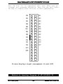
1
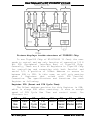
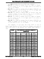
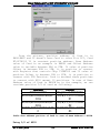
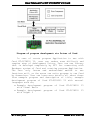
User Manual For ET-PCI8255 V3 Card
ET-PCI8255 V3
General Characteristics of Card ET-PCI8255 V3
The ET-PCI8255 V3 Card is a Programmable Input/Output
- TTL Logic - 72 Bit Card. It is designed and developed to
connect with a computer PC by PCI Bus System through PCI
SLOT. ETT chooses processed Chip IC No.“TIGER320” from
Tiger Jet Network Inc which is specially designed for
using with PCI Bus. This chip was tested and approved by
PCI-SIG Test and Approved Organization that it can
completely support the connection with PCI Bus V2.2. So,
the user can ensure that its function can support and
connect with the PCI Bus System.
ET-PCI8255 V3 Card will act as an Input/Output TTL
Logic card for expansion the amount of Input/Output of the
computer PC. For Input/Output of the card, ETT chooses 3
Chips of IC - PIO Type (Programmable Input/Output) No.
8255. Each chip has 3-Ports of Input/Output size 8 Bits
(24 Bit I/O). Each port can be programmed independently to
act as Input or Output that make the ET-PCI8255 V3 Card
has 9 Ports of I/O size 8 Bits (72 Bit I/O). All 3 chips
of 8255 of the ET-PCI8255 V3 Card connect with the
computer by the PCI Bus System through the PCI Decoder
Chip No. TIGER320. The 8255 Chip is arranged to connect
with PCI Bus System in I/O Port Level and the function of
TIGER320 Chip is a medium of connection between PCI Bus
and 8255 via I/O Port Level of PCI Function.
Connector I/O(34 Pin
ET-BUS)
Chip PIO(8255) x 3
PIB Bus Buffer +
Decode
↕
I/O Function Register
TIGER320(PCI
DECODER)
PCI Function
Register
↕
PCI SLOT
ETT.CO.,LTD
-1
1-
WWW.ETT.CO.TH
User Manual For ET-PCI8255 V3 Card
Picture1: Operating structure of the ET-PCI8255 V3 Card
In the picture 1, if the user wants to program 8255,
the user needs to do via TIGER320 Chip all the time. This
is because we use TIGER320 Chip as a Decoder of PCI Bus
signal and a communicator for receiving/sending of the
instructions and data between BIOS and ET-PCI8255 V3 Card.
There are many registers contain inside TIGER320 Chip for
communication between PCI Bus and Card. We can separate
the registers inside TIGER320 Chip into 2 groups as
following:
• PCI Function Register: This is a standard Register
group which is used to display and control the
operation of PCI Card in PCI Function level. It is
connected directly with the signal from PCI Slot. It
can be accessed through a special function of BIOS or
PCI Driver only. It is mainly used to display a
status of connection and control the operation of PCI
Card. For example, BIOS will read the value of
manufacturer code, product code, and card type to
classify them into their group so it can supply the
necessary resources for the card correctly. The
additional detail and function of the registers in
this group are available in data sheet of “TIGER32”
Chip.
• I/O function Register: This is a register group to
control I/O operation of TIGER320 Chip. The TIGER320
Chip consists of many functions such as Serial ISDN
Communication, Serial to Parallel Communication, and
Parallel to Serial. Normally, this chip is mainly
used to produce PCI Modem but ETT uses it to connect
with I/O through the function - type PIB (Peripheral
Interface Bus) in the circuit of ET-PCI8255 V3 Card.
It is the only function of the I/O connectionParallel size 8 Bits. To use the card, the user needs
to control this register group to operate the
TIGER320 Chip as designed circuit. This register
group is assigned and arranged the position in the
part of “I/O Function” in PCI by BIOS which has 256
position. We can access by reference to the address
position of “I/O Function” which has 48 Registers and
position of Offset address access range of $00..$2F.
The meaning of Offset Address is the Offset value of
address position that points Base Address value as
start position of “I/O Function”. For example, if
ETT.CO.,LTD
-2
2-
WWW.ETT.CO.TH
User Manual For ET-PCI8255 V3 Card
card is assigned the position of value I/O Address
Range or Base Address as $E800-$E8FF, it means that
position of this Register group operation is $E800$E8FF. The additional information about the function
to operate all Registers is available in data sheet
of TIGER320.
Operational Control of TIGER320
TIGER320 Chip, which is the PCI Interface Chip, is
designed to use mainly for the communication. But for ETPCI8255 V3 Card, this chip act as a decoder and medium for
the connection between PCI Bus and PIO 8255 by PIB
Function (Peripheral Interface Bus). Structure inside
TIGER320 Chip is separated into 2 functions: Function of
connecting with PCI Bus and Function of connecting with
User I/O.
● Function of connecting with PCI Bus consists of
connection circuit and decoder of PCI Bus 32 Bits
data that can support connection with Bus PCI V2.2
system perfectly. This part consists of PCI
Configuration Register and Bus Decoder that can
support connection with PCI Bus V2.2 perfectly as
all specifications of PCI Sign and is warranted
standard PCI from PCI Sig.
● Function of connecting with User I/O consists of
Parallel connection circuit 8 Bits PIB and Serial
connection circuit. There are 48 registers to
control and operate.
ETT.CO.,LTD
-3
3-
WWW.ETT.CO.TH
User Manual For ET-PCI8255 V3 Card
Picture displays inside structure of TIGER320 Chip
To use Tiger320 Chip of ET-PCI8255 V3 Card, the user
needs to control and use only function of connection I/O 8
Bit PIB (Peripheral Interface Bus) of Tiger320 Chip.
Generally, There are 8 bits 48 Registers in Tiger320 Chip
for controlling and connecting with both Parallel and
serial I/O. A position of Offset Address to access is
between 00H to 2FH. In this case, we will only mention
about
3
Registers
that
relate
with
PIB
Parallel
Connection. The specifications and functions for each
Register as following:
Register PIB (Reset and PIB Cycle Time)
The Offset address position for this Register is 00H,
which is always 00H after resetting. It uses to assign
speed of PIB Cycle Bus Time and control reset. Its
Structure is:
D7
DMA
Bus
Mode
D6
DMA
Int.
Mode
ETT.CO.,LTD
D5
PIB
Cycle
Time
D4
PIB
Cycle
Time
D3
Reserv
e
-4
4-
D2
Reset
Serial
Port
D1
D0
Reset Reset
Master EXTR
ST#
WWW.ETT.CO.TH
User Manual For ET-PCI8255 V3 Card
• DMA Bus Mode (DMA Bus Master Operation Mode): It uses
to assign DMA action. If assigned as “0”, it means
that assigning TIGER320 runs normally and if assigned
as “1”, it means that assigning runs as DMA. We
always assign value for ET-PCI8255 V3 as “0” because
we don’t use DMA.
• DMA Int. Mode (DMA Interrupt Mode): It assigns to
display the status of Interrupt from DMA. If assign
Bit as “0”, it means that Bit status of Interrupt is
set as “1” when DMA Address has value as same as
Interrupt Address value or End Address value only. If
assigned Bit as “0”, it means that Bit status of
Interrupt is set forever until reset a new one by
writing “1” at Bit status. We always assign value for
ET-PCI8255 V3 as “0” because we don’t use Interrupt.
• PIB Cycle Time: It uses to assign speed of PIB Cycle
for reading the signal from PIB Bus by using Bit 5
and 4 together. There are 3 levels of it;
○ 0:0 It assigns PIB Cycle Time value as 3 Cycle of
PCI Bus (Fastest).
○ 0:1 It assigns PIB Cycle Time value as 8 Cycle of
PCI Bus.
○ 1:X It assigns PIB Cycle Time value as 15 Cycle of
PCI Bus (Slowest).
• Reset Serial Port: It uses for Serial Communication
resetting. If assigned as “0”, it means that Serial
communication run as normally. If assigned as “1”, it
means to reset Serial communication. We always assign
value for ET-PCI8255 V3 as “0” because we don’t use
Serial Communication.
• Reset Master (Reset DMA Logic) It uses for DMA
operation resetting. If assigned as “0”, it means
that it runs as normally. If assigned as “1”, it
means to reset DMA. We always assign value for ETPCI8255 V3 as “0” because we don’t use DMA.
• Reset EXTRST# (EXTRST# Pin State) It uses for
assigning Logic status to signal pin EXTRST# that is
a Reset signal pin of PIB. If assigned Bit as “0”, it
means that signal Logic “0” is sent by Reset signal
pin when resetting. If assigned Bit as “1”, it means
that signal Logic “1” is sent by Reset signal pin
when resetting.
ETT.CO.,LTD
-5
5-
WWW.ETT.CO.TH
User Manual For ET-PCI8255 V3 Card
Notice:
EXTRST# Signal in ET-PCI8255 V3 Board is decoded
with RST# signal which is a Reset signal from PIB. Output
signal that receives from decoding will be sent as a
RESET# signal to control the 8255 Resetting again. So, we
always assign the working status of EXTRES# signal as “0”.
AUXC Register (PIB AUX Port Control)
The Offset address position for this register is 02H,
which is always 00H after resetting. This register is used
to assign the function of AUX (0..7) signal pin. If
assigned whichever Bit as “0”, it means AUX signal of that
Bit will run as Input Port. If assigned whichever Bit as
“1”, it means AUX signal of that Bit will run as Output
Port. Its structures are;
D7
D6
D5
D4
D3
D2
D1
D0
AuxC7 AuxC6 AuxC5 AuxC4 AuxC3 AuxC2 AuxC1 AuxC0
• AuxC(0..7) is used for assign function of AUX(0..7)
signal. So AuxC0 and AuxC7 are used to assign
function of AUX0 and AUX7 signal sequentially.
AUXD Register (PIB AUX Data Port)
The Offset address position for this register is 03H,
which is always 00H after resetting. This register has 2
functions. First, in the case of writing data to this
port, it assigns the Logic status of Output signal to AUX
signal, which is assigned a function as Output. On the
other hand, if any AUX signal is assigned function as
Input, data that wrote to this Register will have no
effect to the AUX signal of that Bit. Second, in the case
of data reading from this Register, it read the status of
AUX signal. If AUX signal of whichever Bit is assigned
function as Output, the reading value of it will be an
Output Latch or the last Output status that written. On
the other hand, if AUX signal of whichever Bit is assigned
function as Input, the reading value of it will be an
actual Input status of that AUX signal Bit. Its structures
are;
D7
D6
D5
D4
D3
D2
D1
D0
AuxD7 AuxD6 AuxD5 AuxD4 AuxD3 AuxD2 AuxD1 AuxD0
• AuxD(0..7) is used for assign the Output value or
display Input/Output status of AUX(0..7) signal. So
ETT.CO.,LTD
-6
6-
WWW.ETT.CO.TH
User Manual For ET-PCI8255 V3 Card
AuxD0 and AuxD7 are used to assign function of AUX0
and AUX7 signal sequentially.
Notice:
For ET-PCI8255 V3 Card, it uses 2 Bits of AUX
signal, which are AUX0 and AUX4. AUX0 is used as the
signal to control the decoder position of 8255. The user
always need to assign the function of AUX0 signal as
Output with “0” status, otherwise user can not run 8255 in
Card. AUX4 signal is used to control RELAY and always need
to be assigned a function as Output. If AUX4 signal value
is “0”, it will command ‘ON RELAY’. But if AUX4 signal
value is “1”, it will command ‘OFF RELAY’.
Basic of Using I/O Port 8255
Generally, PIO Chips No.8255, which is I/O 8 Bit can
be adapted to use well in many Input/Output works. It is
very popular because it’s not complicate and easy to use.
ETT.CO.,LTD
-7
7-
WWW.ETT.CO.TH
User Manual For ET-PCI8255 V3 Card
We’re
always
found
it
in
Microprocessor
and
Microcontroller circuit that require more support from I/O
instrument, additional from it in CPU.
8255 can be programmed into 3 modes and each 8255
port can be programmed as Input or Output. 8255 has 3 I/O
Ports size 8 Bits and 1 Controller Port. The user can
command, read, write, and use 8255 through any ports by
selecting 4 register positions inside 8255. When ETPCI8255 V3 Card is assigned to work with Chip PCI Decoder,
it is designed in part of connection with 8255 by decoding
the address position for reading and writing 8255 as
following;
8255 Position
IC 8255
No.#1
IC 8255
No.#2
IC 8255
No.#3
ETT.CO.,LTD
Port = Function
PA = Input / Output
Port
PB = Input / Output
Port
PC = Input / Output
Port
PCC = Control 8255
PA = Input / Output
Port
PB = Input / Output
Port
PC = Input / Output
Port
PCC = Control 8255
PA = Input / Output
Port
PB = Input / Output
Port
PC = Input / Output
Port
PCC = Control 8255
-8
8-
Offset Address
Position
Base Address +
C0H
Base Address +
C4H
Base Address +
C8H
Base Address +
CCH
Base Address +
D0H
Base Address +
D4H
Base Address +
D8H
Base Address +
DCH
Base Address +
E0H
Base Address +
E4H
Base Address +
E8H
Base Address +
ECH
WWW.ETT.CO.TH
User Manual For ET-PCI8255 V3 Card
Table displays the allocation of the address position of 8255
inside Card ET-PCI8255 V3
Notice:
The meaning of Base Address value is I/O Base
Address Value or I/O Address Range Value. It is a basic
address position for connecting with I/O of card that is
allocated the position from BIOS. Before connecting to run
8255 in ET-PCI8255 V3 Card, the user need to assign the
function of AUX0 signal as Output Port and its status
value is “0.
There’re 3 modes to run in 8255 as following;
Mode 0 It is a basic Input/Output Mode which the user
can assign all 3 of 8255 Ports: Port-A, Port-B and Port-C
to be Input or Output as required. This mode is popular.
Mode 1 It is special Input/Output Mode which can
detect each other signal (HandShake). It’s used for
send/receive parallel data. User can assign Port-A and
port-B as Input or output. For Port-C, it is separated
into 2 parts: Port-C Upper (PC4-PC7) and Port-C Lower
(PC0-PC3). Port-C Upper (PC4-PC7) is used to check how
ready of Port-A in sending/receiving of data. Port-C Lower
(PC0-PC3) is used to check how ready of Port-B in
sending/receiving of data. The system in this mode is as
same as SPI system of CPU.
Mode 2 It is another special mode that used to
send/receive parallel data as in Mode 1 but it uses only
Port-A to send/receive data and uses Port-C to control and
check how ready in sending/receiving of data. This mode is
better than Mode 1 because function of Port-A will be Bidirectional signal that can be both Input and Output. In
addition, user can program Port-B to run in mode 0 as
normal Input/Output because Port-B will not be used in
this mode.
Generally, user usually uses 8255 in Mode 0, which is
a basic Input/Output Mode. So before using 8255, user need
to assign function of 8255, mode of working, Input and
Output port by sending “Control Word” of 8255 to the
controller Port of 8255.
In case of using 8255 in ET-PCI8255 V3 Card, user
have to run 8255 through PIB Function of TIGER320 Chip
again
because
RESET
controller
signal
and
Decoder
controller signal of 8255 are controlled by EXTRST# signal
and AUX0 signal of TIGER320 respectively. So, before
running 8255 in ET-PCI8255 V3 Card, user needs to assign
ETT.CO.,LTD
-9
9-
WWW.ETT.CO.TH
User Manual For ET-PCI8255 V3 Card
function of EXTRST# signal and AUX0 signal correctly as
following;
- Assign function of EXTRST# signal to run as Active
“0” through Register PIB (Offset : 00H)of TIGER320
- Assign function of AUX0 as Output with “0” value.
It will start decoder position circuit which the
Chip Select (CS#) is used to control 8255 by
commanding from AUXC Register (Offset: 02H) and
AUXD Register (Offset: 03H) of TIGER320.
In the first time, user need to send “Control Word”
to 8255 Controller Port for assigning 8255 to acknowledge
its function. The size of 8255 controller Code is 8 Bits.
The meaning of each Bit as folowing;
Picture displays meaning of Bit Cotroller in 8255
• Bit D7 It’s used for mode setting to control 8255
operation for acknowledging the command code in the
other Bits. It will run at Logic “1”. So, if the user
wants to use this function, user have to assign Bit
D7 as “1” in Control Word.
• Bit D6 and D5 They’re used for Mode assigning of
Port-A to 8255. User can assign into 3 modes;
○ 00 = Assign Port-A of 8255 run in Mode 0
ETT.CO.,LTD
-10
1010
WWW.ETT.CO.TH
User Manual For ET-PCI8255 V3 Card
•
•
•
•
•
○ 01 = Assign Port-A of 8255 run in Mode 1
○ 1X = Assign Port-A of 8255 run in Mode 2
Bit D4 It’s used to assign Port-A as Input or Output.
If its value is “1”, it is Input and If its value is
“0”, it is Output.
Bit D3 It’s used to assign Port-C Upper (PC4-PC7) as
Input or Output. If its value is “1”, it is Input and
If its value is “0”, it is Output.
Bit D2 It’s used to assign Mode of Port-B. User can
choose 2 modes. If its value is “0”, it is in Mode 0
and If its value is “1”, it is in Mode 1.
Bit D1 It’s used to assign Port-B as Input or Output.
If its value is “1”, it is Input and If its value is
“0”, it is Output.
Bit D0 It’s used to assign Port-C Lower (PC0-PC3) as
Input or Output. If its value is “1”, it is Input and
If its value is “0”, it is Output.
For example, if you want the first 8255 to run in
Mode 0 and function of all Ports are Output, you need to
write 80H value to the Address Port number Base Address +
CCH.
Code
Control
Word
80H
81H
82H
83H
88H
89H
8AH
8BH
90H
91H
92H
93H
98H
99H
9AH
ETT.CO.,LTD
The Result of Function Status of
8255 Port
Port-A
Port-B
Output
Output
Output
Output
Output
Output
Output
Output
Input
Input
Input
Input
Input
Input
Input
Output
Output
Input
Input
Output
Output
Input
Input
Output
Output
Input
Input
Output
Output
Input
-11
1111
PortCHigh
Output
Output
Output
Output
Input
Input
Input
Input
Output
Output
Output
Output
Input
Input
Input
PortCLow
Output
Input
Output
Input
Output
Input
Output
Input
Output
Input
Output
Input
Output
Input
Output
WWW.ETT.CO.TH
User Manual For ET-PCI8255 V3 Card
9BH
Input
Input
Input
Input
Table Show the conclusion of 8255 Control Word in Mode 0
Installing Card ET-PCI8255 V3
It is not difficult to install ET-PCI8255 V3 Card
into Slot PCI of computer, user only open the computer
case cover and insert card into Slot PCI and then screw
tightly. In this installing step, user should pay
attention and be careful. Process of installing ET-PCI8255
V3 Card as following;
• First, shut down computer with take off any plug,
and then open Case cover of computer for
installing ET-PCI8255 V3 Card into Slot PCI. User
should pay attention and be careful. Make sure
the inserted Card and Slot PCI are tightly match
and don’t connect any accessaries with computer
while installing Card in the first time. Other
I/O accessaries such as Board Output RELAY, Board
OPTO-Input,
you
can
install
later.
After
installing Card completely, you
can
supply
electricity into computer and boot it together.If
computer doesn’t run as normally, you must turn
off the computer, find the cause of the problem,
and solve it. If there’s nothing wrong, computer
will run as normally.
• Installing Driver into Card that will be done
only once in the first time. In Boot step of
Windows program, Windows will check all incoming
installation automatically. Board ET-PCI8255 V3
provides Driver of Card to install completely but
there’s some different characteristics of message
display box that help to install in each Windows
Program. The important thing to install is
assigning to install Driver as Manual by selected
Driver from CD-ROM that save file Driver of Card
and doesn’t assign function of Windows Program to
find Driver automatically. In this case, we would
introduce an example of proceeding to install
Driver for using with Windows-XP only, user may
be adapt its for other Windows program as message
display box. After installed Card ET-Pci8255 V3
into Slot PCI completely and Boot computer in the
first time, Windows Program will check Hardware
automatically and then display message about
ETT.CO.,LTD
-12
1212
WWW.ETT.CO.TH
User Manual For ET-PCI8255 V3 Card
incoming Hardware installation and ask for the
Driver of Card as in the picture.
In this step, select “Install from a list or specific
location (Advance)” and then select “Next”
ETT.CO.,LTD
-13
1313
WWW.ETT.CO.TH
User Manual For ET-PCI8255 V3 Card
In this step, assign position of Driver by select
“Browse” with assign position address of Card Driver in
CD-ROM and then select “Next”
After specify location of Driver completely, program
will start to install Driver into Windows immediately.
Wait until completely and select “Finish” as in the
picture. This is the finish step of driver installation.
ETT.CO.,LTD
-14
1414
WWW.ETT.CO.TH
User Manual For ET-PCI8255 V3 Card
After installed Driver completely, user need to
install Library Driver for additional program developing.
To do that the user has to open the folder that save
Driver file. Then command file running for installing
Library Driver of Card. Create 2 Bat files: Install-xp.bat
and Install-98.bat. If it is Windows 95/98/Me, Select
Install-98.bat file but if it is Windows 2000/NT/XP,
select Install-xp.bat file by double click at icon of file
as in the picture.
After the driver was installed in your computer, when
you boot computer next time, it will check Card in the
system automatically and ready to run immediately. After
this you can install other accessaries that connect with
Card such as Board RELAY or INPUT/OUTPUT OPTO ISOLATE by
shut down Windows and install them as required.
Checking the Card Location
ETT.CO.,LTD
-15
1515
WWW.ETT.CO.TH
User Manual For ET-PCI8255 V3 Card
After installed the Driver to ET-PCI8255 V3 Card
completely, user can check it by click Contol Panel →
System → Hardware →Device manager as in the picture.
If there’s no any problem about installing Driver,
Windows will display all installed and you will see ETPCICARD as in the picture. When user click on plus sign in
front of ET-PCICARD, it will display list of Card ETPCI8255 V3 as name of CARD-1 to 4 depend on assign Jumper
to select ID Code. User can install 4 ET-PCI8255 V3 Card
per a computer but user need to assign number of ID Code
differently. For example, assign number of ID Code as
range 1 to 4 respectively and if install only one card,
should always assign number of ID Code as 1.
Double click at list of Card that will display card
Properties and then select “Resources” for check location
of Card as in the picture.
ETT.CO.,LTD
-16
1616
WWW.ETT.CO.TH
User Manual For ET-PCI8255 V3 Card
From the picture, position address of Card is in
E800-E8FF and if doesn’t move Card to other Slot PCI, Card
ET-PCI8255 V3 is constant position address. Base Address
value of Card in an example is E800H and Offset Address
value is variable between 00H to FFH. If value of position
Offset is between 00H to 2FH, it is position to connect
with Register that controls Chip TIGER320 and If value of
position Offset is between C0H to FFH, it is position to
connect with PIB Function. Card is decoded these positions
to connect with 8255 amount 12 positions. In case of Base
Address value of Card is E800H as in the example, we can
conclude position I/O of card as following;
Address
Device
E000H-E02FH
Register of TIGER320
E0C0H,E0C4H,E0C8H,E0 PA,PB,PC,PCC of 8255
CCH
#1
E0D0H,E0D4H,E0D8H,E0 PA,PB,PC,PCC of 8255
DCH
#2
E0E0H,E0E4H,E0E8H,E0E PC,PB,PC,PCC of 8255
C
#3
Table Show address position of Card in case of Base Address = E000H
Using I/O of 8255
ETT.CO.,LTD
-17
1717
WWW.ETT.CO.TH
User Manual For ET-PCI8255 V3 Card
3-I/O signal of 8255 is connected external to 3-IDE
Port 34 Pin. It is separated into each 8255 and all
3-signal are arranged similarly. User can use Pair Cable
34 Pins to connect with IDE Port of 8255 immediately.
PA 0
PA 1
PA 2
PA 3
PA 4
PA 5
PA 6
PA 7
PB0
PB1
PB2
PB3
PB4
PB5
PB6
PB7
PC0
PC1
PC2
PC4
PC3
PC5
PC6
PC7
+V CC
GND
Picture displays signal arrangement of each 8255
Method to develop Program of ET-PCI8255 V3
ETT.CO.,LTD
-18
1818
WWW.ETT.CO.TH
User Manual For ET-PCI8255 V3 Card
To write program for connecting with ET-PCI8255 V3
Card, the user needs to access to the position of ETPCI8255 V3 Card in I/O Port Level. So it will directly
access to the I/O Port position of all 3 - 8255 Chips on
board. The I/O Port system of PCI Bus is allocated the
position by BIOS of computer. Normally, PCI Card will be
allocated the position into 3 parts:
- Position of Memory Function Address - 4 Kbytes
- Position of I/O Port Address(Input/Output Function)
- 256 positions
- Position of Interrupt signal
For ET-PCI8255 V3 Card, we access to I/O Port of
3- 8255 Chips through the address position which is the
“I/O Port Function” of PCI Bus only. We don’t use address
position which is the “Memory Function” and “Interrupt”
because ET-PCI8255 V3 Card has only I/O Port (8255) and
8255 doesn’t support Interrupt Function.
User Application Program
↕
Device Driver
↕
PCI Bus (PCI Bridge)
↕
Card PCI Model : ETPCI8255 V3
PCI
Decoder(TIGER320)+PIO(
8255)
Diagram of the connection of ET-PCI8255 V3 Card with PCI Bus System
If writing program to use ET-PCI8255 V3 Card and that
program’s platform runs under DOS, user can access to
address position of I/O Port immediately. It uses I/O Port
function for Input and Output Port which user can learn
these details from document of development Application.
Today, most computers are installed and used with
Microsoft Windows, so we would introduce method to write
program for connecting with Card ET-PCI8255 V3 under
Microsoft Windows only.
For new Windows such as
WindowsNT/2000/XP, there’s no any Input Port and Output
ETT.CO.,LTD
-19
1919
WWW.ETT.CO.TH
User Manual For ET-PCI8255 V3 Card
Port function in program to create Applications such as
Borland Delphi, Borland Builder C++, Visual Basic, Visual
C++ to run under them. It doesn’t allow to connect with
Input Port and Output Port directly because program
Applications that run as Multi Tasking under Windows are
shared time to run for each. If many program Application
can access to I/O Port directly without controller,
resources inside program may be scrambled. For example,
Program Application-1 runs with Serial Port by assign
speed at 9600BPS and Program Application-2 runs with
Serial Port, too but it may be different speed. If user
use both Program Application-1 and program Application-2
in the same time, both of them can access to I/O Port of
Serial Port directly, it makes some problems occur. So,
Windows is assigned program Application can access to I/O
Port through Controller of Windows only. SO if any program
Application which asks and is allowed to access to I/O
Port first doesn’t come back to Windows, other program
Application doesn’t allow to access to that I/O Port.
Windows will announce of usage I/O Port to other program
Application that asks to access in that I/O Port.
Windows allows all program Applications can ask and
access to I/O Port under Windows controller via Kernel
only. I/O Port that is installed and used on computer PC
under Windows need to announce specifications such as
Device Class, Device ID, Product ID, …, to Windows for
selecting position correctly and having Driver for
communication with I/O Port.
To create program Application for using with ETPCI8255 V3 Card, the user needs to run 8255 through Driver
Mode by connecting Kernel of Windows, which the Driver
creation step is difficult and complicate. Most Hardware,
which designed to use with computer PC, are the specified
function hardware so the manufacturers always provide
processed program Application Controller within a pack.
For ET-PCI8255 V3 Card, it is an I/O Card that user can
adapt I/O functions as require. So, the users need to
create program Application by themselves. The users who
write the program have to understand about how to create
Driver for connection with I/O Port while they’re creating
the program application under Driver Mode of Hardware.
Normally, it uses Language C or DDK program (Driver
Development KIT) to create Driver, so programmers need to
understand all Hardware system and specifications of
writing Driver.
ETT.CO.,LTD
-20
2020
WWW.ETT.CO.TH
User Manual For ET-PCI8255 V3 Card
Diagram of program development via Driver of Card.
In case of create program Application to use with
Card ET-PCI8255 V3, user can reduce some difficult and
complex step of development Driver. User can use Library
that is developd completely by ETT for connecting with
Hardware system of Card and creating program Application.
The User only learns and understands method to use
functions well, so the users can write program to run Card
by themselves. User can learn more details all about these
from example program and description of title, example
development program of Card ET-PCI8255 V3 with several
languages such as;
• Example development program of Card ET-PCI8255 V3
with Visual Basic
• Example development program of Card ET-PCI8255 V3
with Delphi 5
ETT.CO.,LTD
-21
2121
WWW.ETT.CO.TH