1
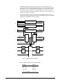
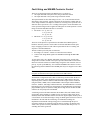
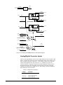
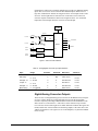
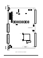
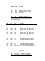
g
GEI-100310
GE Industrial Systems
Bridge Interface Board
IS200BICRH_A_ _
Safety Symbol Legend
These instructions do not purport to cover all details or variations in equipment, nor to
provide every possible contingency to be met during installation, operation, and
maintenance. If further information is desired or if particular problems arise that are not
covered sufficiently for the purchaser’s purpose, the matter should be referred to GE
Industrial Systems.
Indicates a procedure or
condition that, if not strictly
observed, could result in
personal injury or death.
This document contains proprietary information of General Electric Company, USA, and
is furnished to its customer solely to assist that customer in the installation, testing,
operation, and/or maintenance of the equipment described. This document shall not be
reproduced in whole or in part, nor shall its contents be disclosed to any third party
without the written approval of GE Industrial Systems.
Section
Indicates a procedure or
condition that, if not strictly
observed, could result in
damage to or destruction of
equipment.
Note Indicates an essential or
important procedure or
statement.
Page
Functional Description ............................................................................................. 1
Line Voltage Feedback...................................................................................... 3
Motor Voltage Feedback ................................................................................... 4
Motor Current Feedback ................................................................................... 5
Fault Sring and MA/MB Contactor Control ...................................................... 7
Analog/Digital Converter Inputs ....................................................................... 8
Digital/Analog Converter Outputs..................................................................... 9
Discrete Digital Inputs..................................................................................... 10
Solid State Relay Digital Outputs.................................................................... 11
Application Data..................................................................................................... 11
Renewal/Warranty Replacement............................................................................. 15
How to Order a Board ..................................................................................... 15
Handling Precautions....................................................................................... 16
Replacement Procedures ................................................................................. 16
Functional Description
The IS200BICR Bridge Interface Board (BICR) is used in Innovation Seriesä
Medium Voltage - GP, Type H drives. It provides an interface between the bridge
and the drive control. Analog feedback signals from the bridge are connected to TB1
and TB2 on the BICR board's faceplate. These signals are scaled and converted to
voltage controlled oscillator (VCO) signals and then passed to the IS200DSPX
Digital Signal Processor Control Board (DSPX). Basic bridge cell hardware control,
protection, and diagnostics are implemented on the Medium Voltage Ac Drive FiberOptic Hub (FOHB) board. The FOHB board functions are interfaced to the control
through the IS200BPIR Digital Interface Board (BPIR).
The BPIR and BICR boards are mounted in an Innovation Series board rack and
connect to the IS200CABP Cable Assembly Backplane Board (CABP) through their
P1 connectors (also P2 connector for BICR board). The logic signals from the BPIR
board are interfaced to the BICR board through the CABP board.
Innovation Series is a trademark of General Electric Company, USA.
The BICR board also provides a panel and system fault string interface, eight
optically isolated discrete digital inputs and outputs, two 0-20 mA analog feedback
inputs and one 0-10 V analog feedback input. Bridge control, fault string, isolated
I/O, and the 0-20 mA connections are made through the P1 connector. The main
control board interface and logic power supply connections are made through the P2
connector (see Figure 1 and Table 1).
A serial 1024-bit memory device is provided on the BPIR board. This memory is
programmed with board identification and revision information and accessed through
a single data line (BRDID) on the P1 connector.
A
B
C
Line Voltage Feedback
VCO1 LVAB
VCO6 LVBC
A
B
C
Motor Voltage Feedback
VCO4 MVAB
VCO5 MVBC
TB1
P2
V Neutral
B
TB2
IOC A,B &C
P1
P2
IOC Trip V
Ref A
A/D
D/A
Ref B
0-20 mA B
P1
Ref C
XBUS Add, Data & Control
P1
ISO DIG
Ins
P2
Clock
Watchdog
Logic
P2
VCO3 MIC
TEMP
0-20 mA A
P1
VCO2 MIB
Motor Current Feedback
C
EPLD
Spare BPIR Connections
ISO DIG
8 Outs
P!
Contactor
EStop
Logic
P1
PLO BPIR I/O Connections
P1
Figure 1. BICR Board Block Diagram
Table 1. BICR Board Typical Power Requirements
Voltage
Current
+05 V dc
300 mA
+15 V dc
150 mA
-15 V dc
150 mA
+24 V dc (Isolated)
2 · IS200BICR Board
50 mA
GEI-100310
Line Voltage Feedback
BICR board voltage to
frequency gain errors are less
than ±1.7%.
Two line-to-line ac input voltages (LVA-B and LVB-C) are derived by resistive
attenuated monitoring of the three input phases. Attenuation strings are connected to
TB1 and the string resistance (Rx) is varied to scale the feedback (see Figure 2). The
two voltages are converted to VCO signals and passed through the P2 connector to
VCO counters on the DSPX board. The VCO is biased so that with 0 V input, the
output frequency is 1 MHz. Full scale is ±1 MHz from the 0 V bias frequency.
Output frequency per peak (pk) input volt can be obtained using the following
formula: (also see Table 2)
Hz/Vpk = 2.37 K * 168492 Hz / ( Rx + .0095 M)
LVA-B
TB1-2
LVB
LVAB
-
VCO
+
P2-A26
VCO1
LVB-C
LVA
-
TB1-1
+
LVC
+
TB1-3
-
LVBC
VCO
P2-B27
VCO6
LVA-C
Figure 2. BICR Board Line Voltage Feedback Diagram
Table 2. BICR Board Line Voltage Outputs (per Input Rx)
RMS L-L
Voltage
GEI-100310
Input Rx
Value
Pk L-L
Voltage
LVFBK
VCO Hz/V
FS LVFBK L-L
Pk Voltage
LVAB LVBC TP
@ RMS L-L
2400
1800000
3394.1
220.683
4400.8
3.143
3000
2200000
4242.6
180.731
5422.4
3.218
3300
2400000
4666.9
165.730
5913.2
3.246
4160
3000000
5883.1
132.688
7385.7
3.276
4800
3500000
6788.2
113.784
8612.8
3.241
6000
4200000
8485.3
94.863
10330.7
3.378
6600
4800000
9333.8
83.029
11803.1
3.252
6900
5000000
9758.1
79.714
12294.0
3.264
7200
5200000
10182.3
76.653
12784.9
3.276
8400
6000000
11879.4
66.449
14748.2
3.313
10000
7200000
14142.1
55.389
17693.0
3.287
11000
7900000
15556.3
50.487
19410.9
3.296
12000
8600000
16970.6
46.382
21128.9
3.303
12500
9500000
18667.6
41.992
23337.8
3.290
13800
10000000
19516.1
39.895
24564.5
3.267
IS200BICR Board · 3
Motor Voltage Feedback
BICR board voltage to
frequency gain errors are less
than ± 1.9%.
Two line-to-line motor output voltages (MVA-B and MVB-C) are derived by
resistive attenuated monitoring of the three output phases. Attenuation strings are
connected to TB2 and the string resistance Rx is varied to scale the feedback. The
two voltages are converted to VCO signals and passed through the P2 connector to
VCO counters on the DSPX board (see Figure 3). The VCO is biased so that with 0
V input, the output frequency is 1.02 MHz. Full scale is ±1 MHz from the 0 V bias
frequency. Output frequency per pk output volt can be obtained using the following
formula: (also see Table 3)
Hz/Vpk = 5 K * 80172.6 Hz / ( Rx + .005 M)
The motor output neutral voltage (VN) is also monitored. This voltage is scaled and
then passed to one of the 10-bit A/D converters that has a ±1 V full scale input (1/2
VN). The VN is scaled through the attenuation strings and the ± full-scale neutral pk
voltage can be obtained using the following formula:
±V pk full scale = 2 V * (Rx + .005 M)/ 5 K
-VAN
MA
TB1-5
+
-VBN
MB
TB1-6
MC
VCO
+
VCO
P2-D26
VCO4
+
-VCN
TB1-7
MVAB
+
MVBC
P2-A27
VCO5
+
VN
+
+
+
To A/D
Converter
2 V Ref
Figure 3. BICR Board Motor Voltage Feedback Diagram
4 · IS200BICR Board
GEI-100310
Table 3. BICR Board Motor Voltage Outputs (per Input Rx)
RMS L-L
Voltage
Input Rx
Value
Pk L-L
Voltage
MVFBK
VCO Hz/V
FS MVFBK LL Pk Voltage
MVAB MVBC
TP @ RMS L-L
2400
1800000
3394.1
222.640
4401.7
3.163
3000
2200000
4242.6
182.169
5379.6
3.237
3300
2400000
4666.9
166.991
5868.6
3.264
4160
3000000
5883.1
133.599
7335.4
3.294
4800
3500000
6788.2
114.516
8557.8
3.258
6000
4200000
8485.3
95.432
10269.1
3.395
6600
4800000
9333.8
83.504
11736.0
3.268
6900
5000000
9758.1
80.165
12224.8
3.280
7200
5200000
10182.3
77.082
12713.7
3.291
8400
6000000
11879.4
66.805
14669.6
3.328
10000
7200000
14142.1
55.672
17603.1
3.302
11000
7900000
15556.3
50.739
19314.5
3.311
12000
8600000
16970.6
46.609
21026.0
3.318
12500
9000000
17677.7
44.538
22003.7
3.302
13200
9500000
18667.6
42.194
23226.1
3.304
13800
10000000
19516.1
40.084
24448.7
3.282
Motor Current Feedback
The two motor output current voltage signals, IB and IC, are derived by monitoring
the B and C output phase currents using open or closed loop hall effect or LEM™
sensors connected to TB1 and TB2 (see Figure 4). The front end sensor differential
amplifier circuits can be configured for multiple inputs and gains of unity (0.5 and
0.25) through various sensor connection schemes to TB1 and TB2. In high current
applications requiring two sensors per phase, the sensors should be connected as
shown in the parallel sensor connection diagram (see Figure 5).
Note External burden resistors are required when using closed loop sensors. The
burden resistor value should be selected to produce ± 10 V across the burden resistor
with ± full scale sensor output current.
IB and IC voltages are converted to VCO signals (MIB and MIC) and passed through
the P2 connector to the DSPX board VCO counters. The VCO is biased, so that with
0 V at IB and IC the output frequency is 1 MHz. Full scale is ± 1 MHz from the 0 V
bias frequency and is produced with a ± 5 V pk at IB or IC. BICR board voltage-tofrequency gain errors are less than ± 1.7%. Peak full scale is also represented as ± 5
V at the MIA, MIB, and MIC test points.
IA voltage is derived from the inverted sum of IB and IC. All three voltages are
passed to window compare circuits to detect for an instantaneous overcurrent (IOC)
condition. The IOC trip thresholds are programmed from one of the outputs of the
D/A converter. Zero to + full scale of the D/A output corresponds to zero full scale of
the sensor current.
GEI-100310
IS200BICR Board · 5
+15
TB1-9
TB1-10
VCO
B
MIB
TB1-12
MIB
-15
P2-B26
VCO2
+15
MIB
TB2-1
-15
TB2-2
IB
-IB FBK
IOCB
Filter
Window
Compare
IOCA
Filter
Window
Compare
IOCC
IA
+
TB2-3
Filter
Window
Compare
TB2-4
+
To EPLD
MIB
TB1-11
MIB
TB2-5
C
MIB
TB2-6
+15
IC
MIB
TB2-7
-15
TB2-8
IOC Ref
-IC FBK
TB2-9
MIC
+
VCO
P2-C26
VCO3
TB2-10
TB2-11
TB2-12
Figure 4. BICR Board Motor Current Feedback Diagram
TB1-4
TB1-5
TB1-6
-IB FBK1
Out
GND
TB1-7
SHLD
IB1P
± 10 V
TB1-8
IB2P
IB1N
Note:
Current is
Negative
TB1-9
IB2N
TB1-10 IB3N
TB1-11
TB1-12
TB2-1
-IB FBK
20 K
IB3P
40 K
10 K
40 K
-
IB
± 5V
+
40 K
40 K
20 K
+15
10 K
-15
GND
Typical single sensor connections. Phase B
TB1-4
TB1-5
Out
GND
Out
GND
SHLD
IB3P
-IB FBK1
TB1-6
± 10 V
TB1-7
IB2P
-IB FBK2
± 10 V
TB1-8
IB1N
TB1-9
IB2N
Note:
Current is
Negative
IB1P
TB1-10 IB3N
TB1-11
TB1-12
TB2-1
+15
-IB FBK
20 K
40 K
10 K
40 K
+
IB
±5V
40 K
40 K
20 K
10 K
-15
GND
Typical Dual Sensor Connections. Phase B
Figure 5. Motor Current Feedback Sensor Connection Diagram
6 · IS200BICR Board
GEI-100310
Fault String and MA/MB Contactor Control
There are two fault sting inputs to the BICR board: (see Figure 6)
· One input dedicated to the panel series string of interlock contacts
· One input dedicated to the system string of interlock contacts
The input terminals for these fault strings are 24 V, 115 V, and common and each
fault string is fuse protected. Typical connections are between the common and one
of the voltage terminals. The inputs are isolated so one string can be operated at 24 V
while the other is operated at 115 V. Loading of the inputs is 20 mA maximum. One
of the specified voltages must be applied to both inputs for normal operation. Current
ratings for the MA and MB contactors are as follows:
·
MA Form C: 6 A @ 125 V ac
.6 A @ 110 V dc
2 A @ 30 V dc
·
MB Form A: .6 A @ 125 V ac
.6 A @ 110 V dc
2 A @ 30 V dc
The states of the inputs are reported back to the DSPX board. Both inputs are
hardware ANDed to provide a master enable for the MA and MB contactor pilot
relays. Dropping out either or both of these inputs while the drive is running will
sequence a controlled shutdown.
The MA contactor pilot relay has two functions:
· Providing a set of Form C contacts to control the main contactor
· Control of the bridge RUN signal to the FOHB board through the HR1/HR2
contact
To pick up this relay, the C Disable and NMAC lines must be low, and the fault
string must be satisfied. An MA sense input is provided and should be used with an
interlock on the MA contactor to inhibit bridge firing if the main contactor does not
pick up. To pick up the MB relay, the C Disable and NMBC lines must be low and
the fault string satisfied. Both the MA and MB pilot relays are dropped out on a WD
fault.
Note Sense input for the MA contactor is 24 - 115 V ac/dc with a loading of 4 - 10
mA peak. No dedicated sense input is provided for the MB contactor.
The hardware configuration assures that if a fault string is broken while the drive is
running, bridge firing will be disabled before the MA or MB contactors drop out.
Sequencing of the contactors and the FOHB board RUN signal is done in software
using the NMAC, NMBC, RUN, and BICDABL control outputs and the MASEN,
LOCFLT, SYSFLT, and bridge feedback fault lines. The BICDABL line is asserted
high during power-up or hard reset configuration of the BICR board's electronically
programmable logic device (EPLD). Taking this line high assures the MA and MB
contactors do not pick up until commanded.
A watchdog circuit in the EPLD monitors the 20 MHz (clk0) and 16 MHz (clk16)
clock signals. If the 20 MHz or 16 MHz clock is not present, bridge firing will be
disabled, and the MA and MB contactors and discrete digital outputs will drop out. If
a clock failure occurs while the bridge is firing, the RUN signal will also be removed.
In addition to the clk0 and clk16 watchdog, two additional watchdogs are
implemented in the EPLD. If bridge firing power is enabled through the power
electronics enable bit, the watchdog toggle bit must be written to an alternate state
within a clkt1 period. The clkt1 period must be less than 20,000 clk0 periods, or a
watchdog fault will be generated.
GEI-100310
IS200BICR Board · 7
P1-B2
MASENP
P1-B4
MASENN
24-115 V
Buffer
EPLD
MASEN
DRVP5
EPLD
P5
MACOM
NMAC
P1-C21
P1-A5
MAC
MANC
BIC_DABL
P5
P5
EPLD
MANO
P1-A3
P1-A1
MBCOM
P1-A7
NMBC
MBC
MBNO
P1-B6
P1-B8
PNF115
PNF24
P1-A9
EPLD
LOCFLT
(PNF)
Local Fault String
P1-D2
LKCOM
P1-C1
P1-C3
LNF115
P5
EPLD
LNF24
SYSFLT
(LNF)
System Fault String
P1-C5
LNFCOM
P5
Figure 6. Fault String and MA/MB Contactor Control Block Diagram
Analog/Digital Converter Inputs
There are four analog/digital (A/D) converter input channels as shown in Table 5 and
Figure 7. Channel one of the A/D converter monitors the motor neutral voltage (VN).
VN is a bipolar voltage that is biased at 1 V for a neutral voltage of 0 V. Full scale
voltage for this input into the A/D converter is ±1 V. Channel two of the A/D
converter monitors a temperature signal sent from the FOHB board and represents
the peak temperature of the cells during normal operation. Full scale at the input
terminals (P1-TEMP and P1-TEMPC) is 10 V. This voltage is used for temperature
fault indication as shown in Table 4.
Table 4. Temperature Fault Inputs
8 · IS200BICR Board
Voltage
Indication
10 V - 8 V
OK
8V-2V
Over Temp Warning
2V-0V
Over Temp Trip
GEI-100310
Channels three and four are externally multiplexed to provide two additional analog
inputs. The auxan line is used to select the two additional inputs. With an auxan
logic low, channels three and four are assigned to the 0-20 mA input circuits. There
are two 0-20 mA inputs that are scaled for zero to full scale on two of the A/D
converter outputs. Channels three and four are assigned to the 0-10 V and board
temperature circuit outputs when the auxan line is asserted high.
2 V Ref
From VN
P1-C30
Ch1
TEMPC
-
TMP
+
P1-C32
Ch2
NACS
ACLK2 8 MHz
TEMP
AD7777
D0 - D9
NWR
P1-D7
P1-D8
P1-D9
P1-D10
AP
AN
0-20 mA
Ch3
BP
BN
0-20 mA
Ch4
From EPLD
I/O XBUS
NRD
Figure 7. A/D Converter Interface
Table 5. Analog/Digital Converter Input Specifications
Input
Range
VN Neutral
±2V
A/D Chnl.
Auxan Bit
A/D Count
Tolerance
1
NA
256 Cnt./V
± 2.5%
NA
102.4 Cnt./V
± 2.5%
0 - 10 V
2
mA Input - B
0 - 20 mA
3
0
48.9 Cnt./mA
± 3.5%
V Input - C
0 - 10 V
3
1
99.9 Cnt./V
± 3.5%
mA Input - A
0 - 20 mA
4
0
48.9 Cnt./mA
± 3.5%
Board Temp
0 - 5 V @ RTD
4
1
204.8 Cnt./V
± 5.0%
Cell Temp
Digital/Analog Converter Outputs
There are four 12-bit digital/analog (D/A) converters on the BICR board (see Figure
8). Three of these outputs are scaled and buffered to provide the bipolar phase
reference required by the bridge PWM modulator located on the FOHB board. The
forth converter is set between 0 to + full scale to set the motor IOC trip reference
level. All four converter data registers are double buffered. The R/W data register are
loaded, and the new values transferred to the analog outputs, at the same time as the
/LD line is asserted low. All registers are set to the midpoint (0 V) when the DARST
line is set high.
GEI-100310
IS200BICR Board · 9
± 10 V
REF A
PLO-43
Ref P10
DADCS
XBUS Ctl
DARST
NDALD
/CS
A0
A1
R/W
/RST
/LD
D11
± 10 V
Ref H
P5
+
+
O1
REF B
PLO-50
O2
ADC8412
XBUS Data
Ref L
O3
D0
± 10 V
+
O4
REF C
PLO-47
Ref N10
± 10 V
+
+
IOCREFN
IOCREFP
Figure 8. Reference D/A Converter Interface Block Diagram
Discrete Digital Inputs
There are eight differential discrete inputs routed to the BICR board from the CTBC
terminal board through the CABP board. The sense of the inputs is such that a high
input on the CTBC results in a high input to the BICR board's EPLD. The discrete
inputs are optically coupled to the control logic. Each input has a yellow LED to
indicate its state. Overvoltage protection up to 60 V is provided.
Note Input voltages above 60 V cause the 7.5 V zener diode to sink to 30+ mA,
causing it to dissipate more than its rated power (250 mW). The zener diode can
handle non repetitive pulses of 10 W for 1 ms.
Table 6. Discrete Input Specifications
Specification
Conditions
Input Range
10 · IS200BICR Board
Min / Typ / Max (Units)
0 to +30 V dc
Loading
Vin = +30 V dc
Max = 20 mA
Positive Threshold
Vin Increasing
Max = +20 V
Negative Threshold
Vin Decreasing
Min = +5 V
Hysteresis
Min = 4.5 V
Turn-On Time
Typ = 3 µs
Turn-Off Time
Typ = 2.8 µs
Rise Time
Typ = 1.6 µs
Fall Time
Typ = 2.2 µs
Isolation Voltage
Min = 2500 V ac rms
GEI-100310
Solid State Relay Digital Outputs
There are eight solid state relay outputs routed from the BICR board to the CTBC
terminal board through the CABP board. A high output from the BICR board's EPLD
results in the output relay being closed and a low output from the EPLD results in the
output relay being opened. The default relay output state is open (EPLD output
pulled low). The relay outputs are optically isolated from the control. Each output has
a yellow LED to indicate its state. Transient voltage suppression is provided to clamp
the output voltage at 32 V.
Note When clamping at 32 V, the zener diodes can withstand up to 30 mA of
current before they exceed their power rating (500 mW). The zeners can handle nonrepetitive pulses of 10 W for 10 ms.
Table 7. Solid State Relay Output Specifications
Specification
Conditions
Min / Typ / Max (Units)
Output Voltage Rating
Max = 28 V dc
Output Current Rating
Max = 0.7 A dc
Turn-On Time
Photovoltaic Relay
Typ = 2.0 ms
Turn-Off Time
Photovoltaic Relay
Typ = 0.5 ms
Isolation Voltage
Min = 4000 V ac rms
Application Data
The BICR board includes two terminal boards, two backplane connectors, eight user
testpoints, eighteen LED indicators, and two fuses. There are no adjustable hardware
devices on the board. Refer to Figure 9 for component locations and the following
tables for descriptions.
Note There are additional testpoints and an additional connector (JTAG) on the
BICR board surface. These are for development use only and not described in this
publication.
Table
Description
8
TB1 Terminal Board
9
TB2 Terminal Board
10
User Testpoints
11
LED Indicators
12
Fuses
Note Backplane connectors P1 and P2 require a custom extender board to access
individual pin signals. Checking of these signals is not a part of standard in-service
testing/troubleshooting procedures and these signals are not described in this
publication.
GEI-100310
IS200BICR Board · 11
FU2
FU1
DS1
DS10
DS11
DS12
DS13
DS14
DS15
DS16
DS17
DS9
DS2
DS3
DS4
DS5
DS6
LVA-B
TP6
LVB-C
TP7
MVA-B
TP2
MVB-C
TP1
COM
TP21
MIA
TP5
MIB
TP3
MIC
TP4
TP19
0MAC
DS18
TP20
0MBC
DS7
DS8
SW43
SW44
SW45
SW46
SW47
SW48
SW49
SW50
I24
TP14
TP15
I24_RTN
TB1
TB1 Connector
TP18
IMOK
IS200BICRH1A
DCOM TP10
CONF_DONE
TP17
QSTATUS
TP16
TP9
TB2
TB2 Connector
P5
JTAG
TP21
BIC_PSOK
P15
TP11
N15
TP12
TP13 ACOM
Figure 9. BICR Board Layout Diagram
12 · IS200BICR Board
GEI-100310
Table 8. TB1 Bridge Feedback Terminal Board Pin Descriptions
Pin
Name
Description
1
LVA
Line Voltage resistive attenuation Phase A input
2
LVB
Line voltage resistive attenuation Phase B input
3
LVC
Line voltage resistive attenuation Phase C input
4
SHLD
Shield Connection
5
IB3P
Phase B current sensor A = .5 + input 3
6
IB1P
Phase B current sensor A = .25 + input 1
7
IB2P
Phase B current sensor A = .25 + input 2
8
IB1N
Phase B current sensor A = .25 – input 1
9
IB2N
Phase B current sensor A = .25 – input 2
10
IB3N
Phase B current sensor A = .5 – input 2
11
P15
+ 15 V Supply
13
N15
- 15 V Supply
Table 9. TB2 Bridge Feedback Terminal Board Pin Descriptions
GEI-100310
Pin
Name
Description
1
ACOM
Analog ± 15 V Common
2
IC3P
Phase C current sensor A = .5 + input 3
3
IC1P
Phase C current sensor A = .25 + input 1
4
IC2P
Phase C current sensor A = .25 + input 2
5
IC1N
Phase C current sensor A = .25 – input 1
6
IC2N
Phase C current sensor A = .25 – input 2
7
IC3N
Phase C current sensor A = .5 – input 3
8
SHLD
Shield Connection
9
MVA
Motor voltage resistive attenuation Phase A input
10
MVB
Motor voltage resistive attenuation Phase B input
11
MVC
Motor voltage resistive attenuation Phase C input
12
SHLD
Shield Connection to Chassis
IS200BICR Board · 13
Table 10. User Testpoints*
Testpoint
Name
Description
TP6
LVA-B
Line Phase Voltage A-B ±5.94 V pk FS
TP7
LVB-C
Line Phase Voltage B-C ±5.94 V pk FS
TP2
MVA-B
Motor Phase Voltage A-B ±5.94 V pk FS
TP1
MVB-C
Motor Phase Voltage B-C ±5.94 V pk FS
TP21
COM
Signal Common
TP5
MIA
Motor Phase A Current ±5 V pk FS
TP3
MIB
Motor Phase B Current ±5 V pk FS
TP4
MIC
Motor Phase C Current ±5 V pk FS
*These user testpoints are accessible through the opening in the BICR
board faceplate and are listed in the order (from top to bottom) that
they are arranged on the board.
Table 11. LED Indicators*
LED
Color
Name
Description
DS1
Green
IMOK
ON when power applied and board functioning properly
DS2
Yellow
DO2
Digital relay number 2 output, ON when closed
DS3
Yellow
DO3
Digital relay number 3 output, ON when closed
DS4
Yellow
DO4
Digital relay number 4 output, ON when closed
DS5
Yellow
DO5
Digital relay number 5 output, ON when closed
DS6
Yellow
DO6
Digital relay number 6 output, ON when closed
DS7
Yellow
DO7
Digital relay number 7 output, ON when closed
DS8
Yellow
DO8
Digital relay number 8 output, ON when closed
DS9
Yellow
DO1
Digital relay number 1 output, ON when closed
DS10
Yellow
DI1
Discrete digital input number 1, ON when active
DS11
Yellow
DI2
Discrete digital input number 2, ON when active
DS12
Yellow
DI3
Discrete digital input number 3, ON when active
DS13
Yellow
DI4
Discrete digital input number 4, ON when active
DS14
Yellow
DI5
Discrete digital input number 5, ON when active
DS15
Yellow
DI6
Discrete digital input number 6, ON when active
DS16
Yellow
DI7
Discrete digital input number 7, ON when active
DS17
Yellow
DI8
Discrete digital input number 8, ON when active
DS18
Yellow
CONF_DONE
ON when contactor control configuration complete
*LEDs DS2 - DS18 that are visible through the faceplate opening are for troubleshooting purposes
and do not need to be observed during normal operation.
Table 12. Fuses
Fuse
14 · IS200BICR Board
Path
Description and Part Number
FU1
Local fault string
250 V, 200 mA; 44A725207-004
FU2
System fault string
250 V, 200 mA; 44A725207-004
GEI-100310
Renewal/Warranty Replacement
How to Order a Board
When ordering a replacement board for a GE drive, you need to know:
· How to accurately identify the part
· If the part is under warranty
· How to place the order
This information helps ensure that GE can process the order accurately and as soon
as possible.
Board Identification
A printed wiring board is identified by an alphanumeric part (catalog) number
located near its edge. Figure 10 explains the structure of the part number.
The board’s functional acronym, shown in Figure 10, is normally based on the board
description, or name. For example, the BICR board is described as the Bridge
Interface board.
IS 200 BICR H# A A A
Artwork revision1
Functional revision1
Functional revision2
Group (variation, G or H)
Functional acronym
Assembly level3
Manufacturer (DS & IS for GE in Salem, VA)
1Backward
compatible
backward compatible
3
200 indicates a base-level board; 215 indicates a
higher-level assembly or added components (such
as PROM)
2Not
Figure 10. Board Part Number Conventions
Warranty Terms
The GE Terms and Conditions brochure details product warranty information,
including warranty period and parts and service coverage. The brochure is
included with customer documentation. It may be obtained separately from the
nearest GE Sales Office or authorized GE Sales Representative.
GEI-100310
IS200BICR Board · 15
Placing the Order
Parts still under warranty may be obtained directly from the factory:
GE Industrial Systems
Product Service Engineering
1501 Roanoke Blvd.
Salem, VA 24153-6492 USA
Phone: +1 540 387 7595
Fax:
+1 540 387 8606
(“+” indicates the international access code required when calling from outside
of the USA.)
Renewals (spares or those not under warranty) should be ordered by contacting the
nearest GE Sales or Service Office.
Be sure to include the following when ordering any warranty or renewal parts:
· Complete part number and description
· Drive serial number
· Drive Material List (ML) number
Note All digits are important when ordering or replacing any board. The factory
may substitute later versions of boards based on availability and design
enhancements. However, GE Industrial Systems ensures backward compatibility of
replacement boards.
Handling Precautions
To prevent component damage caused by static electricity,
treat all boards with static sensitive handling techniques.
Wear a wrist grounding strap when handling boards or
components, but only after boards or components have
been removed from potentially energized equipment and
are at a normally grounded workstation.
Printed wiring boards may contain static-sensitive components. Therefore, GE ships
all replacement boards in antistatic bags.
Use the following guidelines when handling boards:
· Store boards in antistatic bags or boxes.
· Use a grounding strap when handling boards or board components (per previous
Caution criteria).
Replacement Procedures
To prevent electric shock, turn off power to the board,
then test to verify that no power exists in the board
before touching it or any connected circuits.
To prevent equipment damage, do not remove, insert, or
adjust board connections while power is applied to the
equipment.
16 · IS200BICR Board
GEI-100310
Ø To remove the BICR board
1.
Make sure that the drive in which the board resides has been de-energized.
(Refer to the appropriate User's Manual for complete de-energizing procedures,
GEH-6131 for air-cooled drives or GEH-6133 for liquid-cooled drives.)
2.
Open the drive’s control cabinet door, and using equipment designed for high
voltages, test any electrical circuits before touching them to ensure that power
is off.
3.
Grasp each side of the TB1 connector that joins with the board's TB1 and gently
pull the TB1 connector loose. (Individual wires do not have to be removed from
the TB1 connector.)
4.
Repeat step 3 for TB2.
5.
Carefully remove the board from the rack, as follows:
a. Loosen the screws at the top and bottom of the board, near the board ejector
tabs. (The screws are captive in the board faceplate and should not be
removed.)
b. Unseat the board by raising the ejector tabs.
c. Using both hands, gently pull the board from the board rack.
Ø To install the new replacement BICR board
1.
Verify that both fuses are present and good, then slide the board into the correct
slot in the rack.
Because boards are keyed for specific rack slots, inserting
the BICR into the wrong slot can damage the electronics.
GEI-100310
2.
Begin seating the board by firmly pressing the top and bottom of the board at the
same time with your thumbs.
3.
Finish seating the board in the slot by starting and then tightening the screws at
the top and bottom of the board. Tighten the screws evenly to ensure that the
board is seated squarely (2 - 4 in. lb. torque).
4.
Orient the TB1 connector to TB1 in the same position as when removed and
reconnect the TB1 connector to TB1 (ensure that it is properly seated).
5.
Repeat step 4 for TB2.
6.
Close the drive's control cabinet door.
IS200BICR Board · 17
Notes
g
Issue date: 1999-09-22
Ó 1999 by General Electric Company, USA.
All rights reserved.
18 · IS200BICR Board
GE Industrial Systems
General Electric Company
1501 Roanoke Blvd.
Salem, VA 24153-6492 USA
GEI-100310