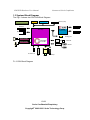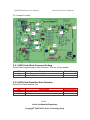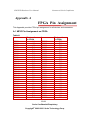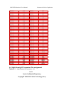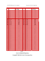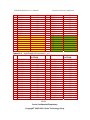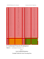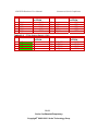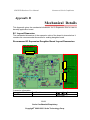
1
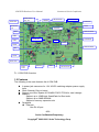
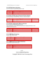
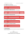
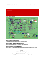
CDK Cheetah Development Kit Hardware User Guide Revision 0.0 1/16/2007 CDK EVB Hardware User Manual Customer & Socle Confidentia Copyright© 2005-2007. Socle Technology Corp. All Rights Reserved. This document contains information that is confidential and proprietary to Socle Technology Corp. and may be disclosed only to those employees of Socle Technology with a need to know, or as otherwise permitted in writing by Socle Technology. Any copying, reproducing, modifying, use or disclosure of this information (in whole or in part) which is not expressly permitted in writing by Socle Technology is strictly prohibited. At a minimum, this information is protected under trade secret, unfair competition, and copyright laws. Violations thereof may result in criminal penalties and fines. Socle Technology reserves the right to change the information contained in this document to improve function, design or otherwise. Socle Technology does not assume any liability arising out of the application or use of this information, or of any error or omission in such information. Any warranties, whether express, statutory, implied or otherwise, including but not limited to the implied warranties of merchantability or fitness for a particular purpose, are excluded. Any license under patent rights or any other intellectual property rights owned by Socle Technology or third parties shall be conveyed by Socle Technology in a separate license agreement between Socle Technology and the licensee. Trademark SoC_ImP®, μPlatform® and the Socle logo, are the trademarks of Socle Technology. All other trademarks referred to herein are the property of their respective owners. 2/29 Socle Confidential/Proprietary Copyright© 2003-2005. Socle Technology Corp. CDK EVB Hardware User Manual Customer & Socle Confidentia Revision History Rev. 0.0 Date 2007/1/16 Description First Version 3/29 Socle Confidential/Proprietary Copyright© 2003-2005. Socle Technology Corp. Author Hank Tsai CDK EVB Hardware User Manual Customer & Socle Confidentia TABLE OF CONTENT PREFACE.......................................................................................................................... 6 ABOUT THE DOCUMENT ................................................................................................... 6 DOCUMENTATION ORGANIZATION.................................................................................... 6 RECOMMENDED INFORMATION FOR FURTHER READING.................................................... 6 CHAPTER 1 ...................................................................................................................... 7 CDK EVB OVERVIEW................................................................................................... 7 1.1 INTRODUCE ................................................................................................................ 7 1.2 FEATURES................................................................................................................... 8 1.3 SYSTEM BLOCK DIAGRAM ....................................................................................... 10 CHAPTER 2 .....................................................................................................................11 SETTING UP AND HARDWARE REFERENCE........................................................11 2.1 INSTALL CDK EVB.................................................................................................. 11 2.1.1 Requirement ......................................................................................................11 Install Steps ................................................................................................................11 2.2 JUMPER SETTING ...................................................................................................... 11 2.2.1 NOR FLASH WRITE PROTECTED SETTING ............................................................ 13 2.2.2 NOR Flash Data Bus Size Selection ................................................................ 13 2.2.3 FPGA Status Selection ..................................................................................... 14 2.2.4 Xilinx FPGA Image Download Chain Setting ................................................. 14 2.2.5 FPGA configuration Mode selection ............................................................... 14 2.2.6 USB Mode Selection ........................................................................................ 14 2.2.7 AMBA Extension Mode Selection .................................................................... 14 2.2.8 VBUS Source Selection .................................................................................... 15 2.2.9 PCI Slot I/O Voltage Selection ......................................................................... 15 2.2.10 PCI Slot I/O Voltage Selection ....................................................................... 15 2.2.11 Cheetah 3.3V Power Connector..................................................................... 15 2.2.12 Cheetah 1.2V Power Connector .................................................................... 15 2.3 SWITCH SETTING ...................................................................................................... 15 2.3.1 System Reset Button ......................................................................................... 16 2.3.2 Design Setting Switch to FPGA ....................................................................... 16 2.3.3 FPGA Re-program Switch ............................................................................... 16 2.3.4 System Power Switch ....................................................................................... 17 2.3.5 GPIO Setting Switch ........................................................................................ 17 2.4 CONNECTORS ........................................................................................................... 17 2.5 LED DISPLAY .......................................................................................................... 18 CHAPTER 3 .................................................................................................................... 20 HARDWARE DESCRIPTION ...................................................................................... 20 3.1 POWER ..................................................................................................................... 20 4/29 Socle Confidential/Proprietary Copyright© 2003-2005. Socle Technology Corp. CDK EVB Hardware User Manual Customer & Socle Confidentia 3.2 RESET ...................................................................................................................... 20 3.3 CLOCK ..................................................................................................................... 21 3.4 MEMORY .................................................................................................................. 21 3.5 SYSTEM EXPAND ...................................................................................................... 22 3.6 Peripherals.......................................................................................................... 22 3.6.1 UART ................................................................................................................... 22 3.6.2 ETHERNET ............................................................................................................. 22 3.6.3 USB ...................................................................................................................... 22 3.6.4 AUDIO ................................................................................................................... 22 3.6.5 LCD...................................................................................................................... 22 3.6.6 GPIO AND SERIAL INTERFACE .............................................................................. 22 APPENDIX A .................................................................................................................. 23 FPGA PIN ASSIGNMENT ............................................................................................ 23 A.1 MFIO PIN ASSIGNMENT ON FPGA.......................................................................... 23 A.2 HIGH DENSITY IO CONNECTOR PIN ASSIGNMENT ................................................... 24 A.3 LOW DENSITY IO CONNECTOR PIN ASSIGNMENT .................................................... 27 APPENDIX B .................................................................................................................. 29 MECHANICAL DETAILS ............................................................................................ 29 B.1 LAYOUT DIMENSION ................................................................................................ 29 Recommend IO Expansion Daughter Board Layout Domension ............................. 29 5/29 Socle Confidential/Proprietary Copyright© 2003-2005. Socle Technology Corp. CDK EVB Hardware User Manual Customer & Socle Confidentia Preface Read This First About the Document This user’s manual describes how to set up, operate and use Cheetah Development Kit (CDK). It has been written for experienced users to getting start in short time. Documentation Organization This document contains the following chapters: Chapter 1 CDK EVB Overview This chapter contains general overview of CDK EVB, including block diagram, main features Chapter 2 Setting up CDK This chapter describes how to start using CDK EVB, including System requirement, how to set up every jumper. Chapter 3 Hardware Description This chapter describes the hardware architecture of CDK EVB in more detail, including power, clock, reset, control, peripherals and bus interface. Appendix A FPGA Pin Assignment Provide detailed FPGA pin assignment. Appendix B Mechanical Dimension Provide mechanical dimension information of IO Daughter Board Recommended information for further reading The list shown below is the recommended information for user’s further understanding to CDK EVB. ▌ AMBA Specification (ARM IHI 0011) ▌ Socle Cheetah chip datasheet ▌ programmer’s guide ▌ Xilinx Spartan-3 datasheet 6/29 Socle Confidential/Proprietary Copyright© 2003-2005. Socle Technology Corp. CDK EVB Hardware User Manual Customer & Socle Confidentia Chapter 1 CDK EVB Overview This chapter gives a brief description of the architecture, features of CDK EVB. It contains the following sections: ▌ Introduce ▌ Features ▌ System Architecture 1.1 Introduce Socle Cheetah Connectivity ASIC includes two major portions -- one is a highly integrated, pre-verified and silicon-proven System-on-Chip (SoC) design platform core, the other is metal programmable logic cells and I/Os. By changing only 4-6 metal layers, fine-grained fabrics implement logic, the metal programmable logic cells allow timing-optimized ASIC-like cell to be built and ensure performance is optimal. The CDK EVB is designed with Socle Cheetah Connectivity ASIC and one on-chip FPGA to emulate on-chip metal programmable logic cells for user to develop, verify application and hardware/software easily. The board also provides clock handling, URAT, MAC, RTC, SDRAM,…etc. circuit and integrated software as a reference design. Fig 1-1 is the overview for CDK EVB. It shows the locations of every component, 7/29 Socle Confidential/Proprietary Copyright© 2003-2005. Socle Technology Corp. CDK EVB Hardware User Manual Static Memory Exp. slot Customer & Socle Confidentia IDE Connector SDRAM SD Connector EJTAG Port JTAG Port Audio Line I/O FPGA NOR Flash RJ45 GPIO Connector USB A Cheetah ASIC LCD Module USB A Mictor FPGA RS232 GPIO Connector PCI RS232 Power Jack Mini PCI Power switch GPIO LCD Connector F1-1 CDK EVB Overview 1.2 Features The following is the main features list of CDK EVB: A power jack connector for 12V AC/DC switching adapter power supply input. Socle Cheetah Chip on baord Support one Xilinx Spatan XC3S4000-FG676 FPGA for user’s design Memory Support up to 16MB Intel StrataFlash for Boot code Support up to 64MB SDRAM Support a memory expansion slot Peripheral Ethernet One RJ-45 port 8/29 Socle Confidential/Proprietary Copyright© 2003-2005. Socle Technology Corp. CDK EVB Hardware User Manual Customer & Socle Confidentia Use IC-Plus IP101A PHY on board UART Two RS232 ports (DB9 type) One 8 pins connector for UART IDE One 2x20 header SD connector Audio Two UDA1342 audio codecs One Line In connector One Line out connector PCI One 32bit PCI slot One 124 pins tpyeIIIA Mini PCI connector LCD 3.5” TFT LCD module on board One 2x25 header for other LCD option USB One A type connector One B type connector Other One IO/Memory Expansion slot Support up to 200 IO pins for system IO and memory expansion One standard 2.54mm 2x17 pin header with I2C, SPI, PWM, GPIO port A, and ADC signals Support LA mictor type debug ports with all set of MFIO signals One JTAG port for ICE debug Seven LEDs to display GPIO port A status One switch with PA0~PA3 for system setting Jumpers for measure Cheetah power consumption 9/29 Socle Confidential/Proprietary Copyright© 2003-2005. Socle Technology Corp. CDK EVB Hardware User Manual Customer & Socle Confidentia 1.3 System Block Diagram The Fig1-2 shows the CDK EVB Block Diagram. Power/Clock/Reset SDRAM Memory Exp. NOR FLASH PCI Slot Cheetah Test Chip FPGA IO Exp. XC3S4000-FG696 Mini PCI Debug port Audio Codec PHY Ethernet Audio Codec Transceiver RS232 EJTAG Port IDE LCD LCD Exp. F1-2 CDK Block Diagram 10/29 Socle Confidential/Proprietary Copyright© 2003-2005. Socle Technology Corp. CDK EVB Hardware User Manual Customer & Socle Confidentia Chapter 2 Setting Up and Hardware Reference This chapter describes how to use the CDK EVB and shows the positions of jumper, headers and connectors. It contains the following sections: ▌ ▌ ▌ ▌ ▌ Install CDK EVB Jumper Setting Switch Setting Connector LED Display 2.1 Install CDK EVB This section describes how to connect hardware components 2.1.1 Requirement The development system should contain the following items at least: ▌ CDK EVB ▌ 12V output power adapter ▌ Multi-ICE or other debug tool ▌ IBM compatible PC Install Steps 1. 2. 3. Plug IO board into CDK AHB Expansion Connector (optional) Switch on power supply Power on ICE To prevent damaging to all boards, make sure to power down before inserting or removing any device. 2.2 Jumper Setting In general, jumpers are used to select options for certain features. On CDK EVB, 11/29 Socle Confidential/Proprietary Copyright© 2003-2005. Socle Technology Corp. CDK EVB Hardware User Manual Customer & Socle Confidentia some of the jumpers are designed to be user-configurable, allowing for system enhancement. The others are for testing purpose only and should not be altered. To select any option, cover the jumper cap over (short) or remove it from the jumper pins. Fig 2-2 is the jumper/connector location diagram for CDK EVB. The default settings shipped from Socle company are marked with a ★. Make sure to have all of configuration jumpers on CDK EVB in the proper location Table 2-1 Jumper List Location JP1 JP2 JP3 JP4 JP5 JP6 J14 JP7 JP8 JP9 JP10 JP11 Function NOR Flash Write Protected Setting Flash Data Bus Size Selection FPGA Status Selection Xilinx FPGA image download chain selection FPGA configuration mode selection USB Mode Selection AMBA Extension Mode Selection VBUS Source Setting PCI Slot I/O Voltage Selection PCI Slot I/O Voltage Selection Cheetah 3.3V Power Connector Cheetah 1.2V Power Connector 12/29 Socle Confidential/Proprietary Copyright© 2003-2005. Socle Technology Corp. CDK EVB Hardware User Manual Customer & Socle Confidentia F2-1 Jumper Location JP1 JP4 JP2 JP3 J14 JP5 JP6 JP7 JP8 JP10 JP9 JP11 2.2.1 NOR Flash Write Protected Setting Select Flash Programming or Write Protected. This is a 1X2 pin header. JP1 ON OFF Description Flash Programming Mode Flash Write Protected Mode Default Setting 2.2.2 NOR Flash Data Bus Size Selection Select Boot Flash data bus size JP2 ON OFF Description Default Setting 8 Bit Mode 16 Bit Mode 13/29 Socle Confidential/Proprietary Copyright© 2003-2005. Socle Technology Corp. CDK EVB Hardware User Manual Customer & Socle Confidentia 2.2.3 FPGA Status Selection Set FPGA status for generating system reset JP3 ON OFF Description FPGA active/No FPGA on board FPGA no image 2.2.4 Xilinx FPGA Image Download Chain Setting Set FPGA image download chain. This is a 1X4 pin header. JP4 1-2, 3-4 2-3 Description Program PROM & FPGA Program FPGA only Default Setting ★ 2.2.5 FPGA configuration Mode selection Select different FPGA configuration mode The configuration mode is selected by setting the appropriate level on the dedicate mode input pins. JP5 Description OFF Master serial mode 1-2, 3-4 ON Parallel Mode Default Setting ★ 2.2.6 USB Mode Selection Select USB function mode JP6 OFF ON Description UDC UHC 2.2.7 AMBA Extension Mode Selection Select Multi-function I/O function. J14 OFF ON Description AMBA Bus CTM MP design interface 14/29 Socle Confidential/Proprietary Copyright© 2003-2005. Socle Technology Corp. CDK EVB Hardware User Manual Customer & Socle Confidentia 2.2.8 VBUS Source Selection Select digital power supply for ARM test chip-A core. JP7 ON OFF Description VBUS from System Board VBUS from Host 2.2.9 PCI Slot I/O Voltage Selection Select PCI Slot I/O in 3.3V or 5V mode. This is a 1X3 pin header. JP8 1-2 2-3 Description Default Setting 3.3V Mode 5V Mode ★ 2.2.10 PCI Slot I/O Voltage Selection Select PCI Slot I/O in 3.3V or 5V mode. This is a 1X3 pin header. JP9 1-2 2-3 Description Default Setting 3.3V Mode 5V Mode ★ 2.2.11 Cheetah 3.3V Power Connector JP10 Description 1-2, 3-4 ON Link 3.3V to Cheetah 1-2, 3-4 OFF No 3.3V to Cheetah 2.2.12 Cheetah 1.2V Power Connector JP11 Description 1-2, 3-4 ON Link 1.2V to Cheetah 1-2, 3-4 OFF No 1.2V to Cheetah 2.3 Switch Setting The section shows the location of all the switches on the board, and describes the function of each switch. 15/29 Socle Confidential/Proprietary Copyright© 2003-2005. Socle Technology Corp. CDK EVB Hardware User Manual Customer & Socle Confidentia Table 2-2 Connector List Location SW1 SW2 SW3, SW4 SW5 Function System Reset Push Button Design Setting Switch to FPGA(Reserved) Xilinx FPGA Re-program Start System Power Switch GPIO Setting Switch F 2-2 Switch Location SW2 SW1 SW3 SW5 SW4 2.3.1 System Reset Button This push button SW2 is provided to reset all system. 2.3.2 Design Setting Switch to FPGA SW2 provides setting pins to FPGA for user’s definition. 2.3.3 FPGA Re-program Switch SW3 restarts or resets download image process from EEPROM to Xilinx FPGA 16/29 Socle Confidential/Proprietary Copyright© 2003-2005. Socle Technology Corp. CDK EVB Hardware User Manual Customer & Socle Confidentia 2.3.4 System Power Switch SW4 switches on/off system power. 2.3.5 GPIO Setting Switch SW5 provides High/Low signal to GPIO Port, 2.4 Connectors The section shows the location of all the connectors on the board, and describes the function of each connector. Table 2-3 Connector List Location Function J1 ICE JTAG Port J2 IDE Connector J3 Download Connector for Xilinx FPGA J4 Static Memory Expansion Slot J5 Audio Line in Port J6 SD Connector J7 Audio Line Out Port J8 Ethernet Port J9 ADC Connector J10 Debug Port to FPGA J11,J15, J17, J18, LA Debug Port (Mictor Type Cnnector) J21 J12 LCD Module Connector J13, J22 IO Expansion Connector J16 USB B-type Port J19 RS232 Port0 J20 RS232 Port2 J23 Mini PCI Connector J24 RS232 Port1 J25 Power Jack J26 I2C/SPI/PWM/GPIO Connector JP12 External LCD Connector PCI_! PCI Slot 17/29 Socle Confidential/Proprietary Copyright© 2003-2005. Socle Technology Corp. CDK EVB Hardware User Manual Customer & Socle Confidentia F 2-3 Connector Location J2 J1 J4 J3 J9 J5 J6 J10 J7 J11 J13 J12 J8 J15 J16 J19 J17 J18 J20 J21 PCI_1 J22 J23 J27 (Back) JP12 J24 J26 J25 2.5 LED Display LED displays are to show board’s condition. Table 2-4 LED Display List Location D1 D2 D3 D4 D5 D6 D7 D8 D9~D16 D18 D19 Description IDE Active MAC COL MAC LINK FPGA Image load Done TXD0 Active RXD0 Active TXD1 Active RXD1 Active GPIO PA Status, 1->light 5V Power OK 3.3V Power OK 18/29 Socle Confidential/Proprietary Copyright© 2003-2005. Socle Technology Corp. CDK EVB Hardware User Manual D20 D21 D22 D23 Customer & Socle Confidentia 2.5V Power OK 1.2V Power OK for FPGA 1.2V Power OK for ASIC 1.8V Power OK for Configuration Flash F 2-4 LED Location D1 D2 D4 D3 D5 D6 D7 D9~D16 D8 D18~D23 19/29 Socle Confidential/Proprietary Copyright© 2003-2005. Socle Technology Corp. CDK EVB Hardware User Manual Customer & Socle Confidentia Chapter 3 Hardware Description This chapter describes hardware of CDK EVB. It contains the following sections: ▌ ▌ ▌ ▌ ▌ ▌ Power Reset Clock Memory Expansion Slot Peripheral 3.1 Power The power for entire CDK EVB Development Board is provided by an external 12V power adapter. Use different regulators to provide power to different components Below is the power scheme of CDK EVB. Power Device/Connector Switching power adapter Cheetah Chip FPGA Image EEPROM NOR Flash/SDRAM MAC PHY PCI/Mini PCI UART Transciver LCD display Audio IO/Memory Expansion Slot Voltage Requirement Provide +12V Core:1.2V IO: 3.3V Core:1.2V AuxPower: 2.5V IO: 3.3V Core:1.8V IO: 3.3V 3.3V 3.3V 3.3V/5V 3.3V 5V/3.3V 3.3V 5V Description 3.2 Reset There are three sources for reset signal 1. TPS3836-E18 output. 2. EJTAG_RSTn from ICE. 3. FPGA configuration Done Signal 20/29 Socle Confidential/Proprietary Copyright© 2003-2005. Socle Technology Corp. CDK EVB Hardware User Manual Customer & Socle Confidentia The reset signal will provide Cheetah ASIC reset and different components through 74LV126 buffer. Press SW1 to generate a Manual reset signal to whole system when power is on. Below is the reset scheme of CDK. nPOR 74LV08 Power Supervisor Cheetah FPGA_Done JTAG_SAST Reset Buffer PCI LCD Memory IO 3.3 Clock All clock sources for devices are listed in the following table. Clock Device Cheetah FPGA Clock Speed 16MHz (Crystal X4) 27MHz (OSC5) 33MHz (OSC6) 48MHz (OSC4) 50MHz (OSC3) 32KHz (Crystal X1) 48MHz (Crystal X3) 12MHz (Crystal X5) 33.8699MHz (OSC1) 48MHz(Crystal X2) (OSC2) Description Main Clock LCD controller PCI USB2.0 and UART RMII RTC USCB2.0 PHY High speed UART Audio CTM MP Design 3.4 Memory The CDK EVB supports one 16MB Intel StrataFlash NOR type Flash, two 32MB SDRAM on board, It also can extend memory through memory expansion slot J4. 21/29 Socle Confidential/Proprietary Copyright© 2003-2005. Socle Technology Corp. CDK EVB Hardware User Manual Customer & Socle Confidentia If the Flash on board is not used, just remove R208. For detailed memory map, please refer to “Cheetah Connectivity Specification”. 3.5 System Expand CDK provides one FPGA (optional) for users to extend system design. There are 133 connections between Cheetah ASIC and FPGA. Set J14 opened, these signals can be AMBA interface, otherwise they will be CTM MP design interface. Besides, 200 pins IO/ expansion slot (J22, J23) provide user to integrate many peripherals circuit on daughter board to meet different application functions. For the pin assignment table and the layout dimension information that provides design reference of daughter board, please refer to Appendix A. 3.6 Peripherals 3.6.1 UART The CDK EVB supports two RS232 ports (J19, J24) and one UART interface connector (J20). Two couples of LED displays (D5, D6 and D7, D8) show the TX and RX signals status. 3.6.2 Ethernet Cheetah provides RMII interface to Ethernet PHY. and RJ45 port for Ethernet application. 3.6.3 USB The EVB provide one USB type A connector and one USB type B connector. User can only use one of them by setting JP6. See Jumper Setting in Chapter 2. 3.6.4 Audio Cheetah can control UDA1342 via I2C interface to have sound features in playback mode. UDA1342 supports I2S-bus data format. Sound data can communicate between Cheetah and Codec via I2S bus. 3.6.5 LCD Cheetah builds-in a TFT/STN LCD controller that supports resolution programmable up to 1024X768. The EVB provides one Amprie’s 3.5” LCD module with 320X240 display resolution and touch screen function. If use other LCD module, JP12 provides all LCD controller interface. 3.6.6 GPIO and Serial Interface The CDK EVB provides one GPIO port, PA[7:0]. 8 LEDs to shows status of these signals for debug. Besides, one connector J26 with serial interface, including I2C, SPI, PWM, and PA[7:0] is provided for IO extension or debug. 22/29 Socle Confidential/Proprietary Copyright© 2003-2005. Socle Technology Corp. CDK EVB Hardware User Manual Customer & Socle Confidentia Appendix A FPGA Pin Assignment This Appendix provides FPGA pin assignment for all devices and connectors. A.1 MFIO Pin Assignment on FPGA TableA.1 Name MFIO0 MFIO1 MFIO2 MFIO3 MFIO4 MFIO5 MFIO6 MFIO7 MFIO8 MFIO9 MFIO10 MFIO11 MFIO12 MFIO13 MFIO14 MFIO15 MFIO16 MFIO17 MFIO18 MFIO19 MFIO20 MFIO21 MFIO22 MFIO23 MFIO24 MFIO25 MFIO26 MFIO27 MFIO28 Pin Location on FPGA A14 A22 A23 D16 E18 F14 F20 G19 C15 C17 D18 D22 E22 B23 C23 E21 F21 B22 C22 C21 D21 A21 B21 D20 E20 A20 B20 E19 F19 Name MFIO67 MFIO68 MFIO69 MFIO70 MFIO71 MFIO72 MFIO73 MFIO74 MFIO75 MFIO76 MFIO77 MFIO78 MFIO79 MFIO80 MFIO81 MFIO82 MFIO83 MFIO84 MFIO85 MFIO86 MFIO87 MFIO88 MFIO89 MFIO90 MFIO91 MFIO92 MFIO93 MFIO94 MFIO95 Pin Location on FPGA D26 E25 E26 G20 G21 F23 F24 G22 G23 F25 F26 G25 G26 H20 H21 H22 J21 H23 H24 H25 H26 J20 K20 J22 J23 J24 J25 K21 K22 23/29 Socle Confidential/Proprietary Copyright© 2003-2005. Socle Technology Corp. CDK EVB Hardware User Manual MFIO29 MFIO30 MFIO31 MFIO32 MFIO33 MFIO34 MFIO35 MFIO36 MFIO37 MFIO38 MFIO39 MFIO40 MFIO41 MFIO42 MFIO43 MFIO44 MFIO45 MFIO46 MFIO47 MFIO48 MFIO49 MFIO50 MFIO51 MFIO52 MFIO53 MFIO54 MFIO55 MFIO56 MFIO57 MFIO58 MFIO59 MFIO60 MFIO61 MFIO62 MFIO63 MFIO64 MFIO65 MFIO66 C19 D19 A19 B19 F18 G18 B18 C18 F17 G17 D17 E17 A17 B17 G16 H16 E16 F16 A16 B16 G15 H15 E15 F15 A15 B15 G14 H14 D14 E14 D13 C13 F22 C25 C26 E23 E24 D25 Customer & Socle Confidentia MFIO96 MFIO97 MFIO98 MFIO99 MFIO100 MFIO101 MFIO102 MFIO103 MFIO104 MFIO105 MFIO106 MFIO107 MFIO108 MFIO109 MFIO110 MFIO111 MFIO112 MFIO113 MFIO114 MFIO115 MFIO116 MFIO117 MFIO118 MFIO119 MFIO120 MFIO121 MFIO122 MFIO123 MFIO124 MFIO125 MFIO126 MFIO127 MFIO128 MFIO129 MFIO130 MFIO131 MFIO132 MFIO133 K23 K24 K25 K26 L19 L20 L21 L22 L25 L26 M19 M20 M21 M22 L23 M24 M25 M26 N19 N20 N21 N22 N23 N24 N25 N26 AA22 AA21 B14 AB23 AC26 AC25 Y21 Y20 AB26 AB25 C14 AA23 A.2 High Density IO Connector Pin assignment TableA.2.1 High Density IO Connector – J9 24/29 Socle Confidential/Proprietary Copyright© 2003-2005. Socle Technology Corp. CDK EVB Hardware User Manual Pin Name 1 3 5 7 9 11 13 15 17 19 21 23 25 27 29 31 33 35 37 39 41 43 45 47 49 51 53 55 57 59 61 63 65 67 69 71 73 75 77 79 P1_1 P1_2 P1_3 P1_4 P1_5 P1_6 P1_7 P1_8 P1_9 P1_10 P1_11 P1_12 P1_13 P1_14 P1_15 P1_16 P1_17 P1_18 P1_19 P1_20 P1_21 P1_22 P1_23 P1_24 P1_25 P1_26 P1_27 P1_28 P1_29 P1_30 P1_31 P1_32 P1_33 P1_34 P1_35 P1_36 P1_37 P1_38 P1_39 P1_40 Customer & Socle Confidentia Pin Location on FPGA B13 F6 E3 E4 D1 D2 G6 G7 E1 E2 F3 F4 G4 G5 F1 F2 H6 H7 G1 G2 J6 H5 H3 H4 H1 H2 K7 J7 J4 J5 J2 J3 K5 K6 K3 K4 K1 K2 L7 L8 Pin Name 2 4 6 8 10 12 14 16 18 20 22 24 26 28 30 32 34 36 38 40 42 44 46 48 50 52 54 56 58 60 62 64 66 68 70 72 74 76 78 80 P1_51 P1_52 P1_53 P1_54 P1_55 P1_56 P1_57 P1_58 P1_59 P1_60 P1_61 P1_62 P1_63 P1_64 P1_65 P1_66 P1_67 P1_68 P1_69 P1_70 P1_71 P1_72 P1_73 P1_74 P1_75 P1_76 P1_77 P1_78 P1_79 P1_80 P1_81 P1_82 P1_83 P1_84 P1_85 P1_86 P1_87 P1_88 P1_89 P1_90 Pin Location on FPGA M1 M2 N7 N8 N5 N6 N3 N4 N1 N2 A3 A5 A6 C4 C8 C12 E13 H11 H12 B3 F7 G10 E5 D5 B4 A4 C5 B5 E6 D6 C6 B6 E7 D7 B7 A7 G8 F8 E8 D8 25/29 Socle Confidential/Proprietary Copyright© 2003-2005. Socle Technology Corp. CDK EVB Hardware User Manual 81 83 85 87 89 91 93 95 97 99 101 102 103 104 105 106 107 108 P1_41 P1_42 P1_43 P1_44 P1_45 P1_46 P1_47 P1_48 P1_49 P1_50 5V 5V 5V 5V 5V 5V 5V 5V TableA.2.2 Pin Name 1 3 5 7 9 11 13 15 17 19 21 23 25 27 29 31 33 35 37 39 P1_101 P1_102 P1_103 P1_104 P1_105 P1_106 P1_107 P1_108 P1_109 P1_110 P1_111 P1_112 P1_113 P1_114 P1_115 P1_116 P1_117 P1_118 P1_119 P1_120 Customer & Socle Confidentia L5 L6 L1 L2 M7 M8 M6 M5 M3 L4 82 84 86 88 90 92 94 96 98 100 109 110 111 112 113 114 115 116 P1_91 P1_92 P1_93 P1_94 P1_95 P1_96 P1_97 P1_98 P1_99 P1_100 GND GND GND GND GND GND GND GND B8 A8 G9 F9 E9 D9 C9 B9 A13 E10 High Density IO Connector – J11 Pin Location on FPGA AE13 AA7 AA13 AB8 AC9 AC11 AD10 AD12 AF4 Y8 AF5 AF13 AE4 AD4 AB6 AA6 AE5 AD5 AD6 AC6 Pin Name 2 4 6 8 10 12 14 16 18 20 22 24 26 28 30 32 34 36 38 40 P1_151 P1_152 P1_153 P1_154 P1_155 P1_156 P1_157 P1_158 P1_159 P1_160 P1_161 P1_162 P1_163 P1_164 P1_165 P1_166 P1_167 P1_168 P1_169 P1_170 Pin Location on FPGA AF12 AE12 Y13 W13 AA5 AD2 AD1 AB4 AB3 AC2 AC1 AB2 AB1 Y7 Y6 AA4 AA3 Y5 Y4 AA2 26/29 Socle Confidential/Proprietary Copyright© 2003-2005. Socle Technology Corp. CDK EVB Hardware User Manual 41 43 45 47 49 51 53 55 57 59 61 63 65 67 69 71 73 75 77 79 81 83 85 87 89 91 93 95 97 99 101 102 103 104 105 106 107 108 P1_121 P1_122 P1_123 P1_124 P1_125 P1_126 P1_127 P1_128 P1_129 P1_130 P1_131 P1_132 P1_133 P1_134 P1_135 P1_136 P1_137 P1_138 P1_139 P1_140 P1_141 P1_142 P1_143 P1_144 P1_145 P1_146 P1_147 P1_148 P1_149 P1_150 5V 5V 5V 5V 5V 5V 5V 5V Customer & Socle Confidentia AF6 AE6 AC7 AB7 AF7 AE7 AB8 AA8 AD8 AC8 AF8 AE8 AA9 Y9 AE9 AD9 AA10 Y10 AC10 AB10 AF10 AE10 Y11 W11 AB11 AA11 AF11 AE11 Y12 W12 42 44 46 48 50 52 54 56 58 60 62 64 66 68 70 72 74 76 78 80 82 84 86 88 90 92 94 96 98 100 109 110 111 112 113 114 115 116 P1_171 P1_172 P1_173 P1_174 P1_175 P1_176 P1_177 P1_178 P1_179 P1_180 P1_181 P1_182 P1_183 P1_184 P1_185 P1_186 P1_187 P1_188 P1_189 P1_190 P1_191 P1_192 P1_193 P1_194 P1_195 P1_196 P1_197 P1_198 P1_199 P1_200 GND GND GND GND GND GND GND GND A.3 Low Density IO Connector Pin assignment TableA.3.1 Low Density IO Connector – J9 27/29 Socle Confidential/Proprietary Copyright© 2003-2005. Socle Technology Corp. AA1 Y2 Y1 W7 W6 V6 W5 W4 W3 W2 W1 V7 U7 V5 V4 V3 V2 U6 U5 U4 U3 U2 U1 T8 T7 T6 T5 T2 AD13 R8 CDK EVB Hardware User Manual Pin Name 1 3 5 7 9 P2_1 P2_2 P2_3 P2_4 P2_5 TableA.3.2 Pin Name 1 2 3 4 Customer & Socle Confidentia Pin Location on FPGA W16 AB14 AD25 Y17 AB22 Pin Name 2 4 6 8 10 P2_6 P2_7 P2_8 P2_9 P2_10 Pin Location on FPGA AC22 AE24 AF24 AE23 AF23 FPGA Setting Switch –SW2 Pin Location on FPGA Pin Name GND GND GND GND 5 6 7 8 SYS_IN0 SYS_IN1 SYS_IN2 SYS_IN3 Pin Location on FPGA AA20 AD15 AD19 AD23 28/29 Socle Confidential/Proprietary Copyright© 2003-2005. Socle Technology Corp. CDK EVB Hardware User Manual Customer & Socle Confidentia Appendix B Mechanical Details This Appendix gives the mechanical dimension for IO Expansion Slot for user to develop application board. B.1 Layout Dimension The mechanical dimension of the expansion slots of the board is shown below. It contains the recommended dimension for making daughter board. Recommend IO Expansion Daughter Board Layout Domension Memory Expansion daughter Board Center to Center 615mil IO Expansion Daughter Board Connector Information Connector Vendor Part Number QTS-050-01-L-D-RA-WT-LS1 SAMTEC Agency Supplier 三顧股份有限公司 29/29 Socle Confidential/Proprietary Copyright© 2003-2005. Socle Technology Corp.