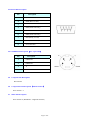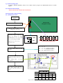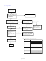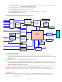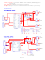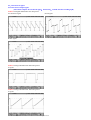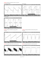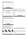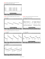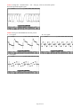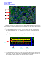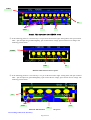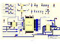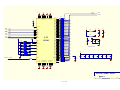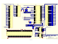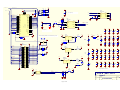
1
OPTIMA Service Manual For PW181 Project: PD5084 PD5084-3TC P5002H PT5058 Etc. Page 0 of 64 THESE DOCUMENTS ARE FOR REPAIR SERVICE INFORMATION ONLY. EVERY REASONABLE EFFORT HAS BEEN MADE TO ENSURE THE ACCURACY OF THIS MANUAL; WE CANNOT GUARANTEE THE ACCURACY OF THIS INFORMATION AFTER THE DATE OF PUBLICATION AND DISCLAIMS RELIABILITY FOR CHANGES, ERRORS OR OMISSIONS. Date:2005/05/18 Page 1 of 64 CONTENTS 1、SPECIFICATION …......................................................................................................…………...….. 1-1 General Specification …................................................….....……........................………....…. 1-2 PDP TV Description.............................................. .............................……………...………….. 1-3 Interface and connection ...................................................................................................…. 1-3-1 Input connection of Video and Audio signal................................................................... 1-3-2 Input connection of PC signal........................................................................................ 1-3-3 Output connection of Video and Audio signal................................................................ 4 4 5 6 6 7 8 2、Interface PIN Description.....................................................................................…………...… 8 8 8 9 9 9 9 9 2-1 D-SUB Pin Description……………………………..…............................................................ 2-2 DVI Pin Description……………………………..…................................. ................................ 2-3 RS-232 Pin Description…………………..….. ....... ................. ............ ................................ 2-4 S-VIDEO Pin Description(Y/C separation)……................................................................... 2-5 Composite Pin Description…………...................... ............................................................. 2-6 Components Pin Description(YPbPr/YCbCr).................................................................... 2-7 Audio Pin Description................................................. ........ .............................................. 3、Operation................................................ .... .....……………...............…………...…………………. 3-1 Operation of Remote Control Transmitter ...........................................................................… 3-2 Front panel controls .....................................................................................................……… 3-3 MENU Function ..............................................................................................................……. 3-3-1 Main MENU ................................................................................................................. 3-3-2 Picture MENU………..…………………………………………...................................... 3-3-3 Sound MENU................................................................................................................ 3-3-4 Setup MENU............................... ................................... . .............................................. 3-3-5 Display MENU............................................................................................................... 3-3-6 Layout MENU(MultiWindows)...................................................................................... 3-3-7 Time MENU.................................................................................................................. 10 10 11 12 12 12 13 14 14 15 16 4、Trouble Shooting Chart.........................................................................................................…..... 4-1 PANEL Trouble shooting………………….........................................................................…… 4-2 Image board trouble shooting………………………............................................................... 4-2-1 No video(PANEL)…………………...................................... ....................................…… 4-2-2 no video(Image board)…………….........................................................................…… 4-2-3 Dynamic single mode defective ................................ ...........................................…… 4-2-4 RGB or DVI mode defective ……......... ...................................................................… 4-2-5 Graphic-Block…………………...............................................................................…… 4-2-6 Video-Block…………………...................................... ............................. ............…… 4-2-7 DC Power-block…………………..............................................................................… 4-2-8 Scaler and LVDS Circuit............................................................................................… 4-3 Tuner board Trouble shooting…………………………………….............................................. 4-4 Audio board Trouble shooting……………………………………………………………………. 4-4-1 DC Power circuit…………………………………. ………………………………………. 4-4-2 Audio circuit…………………………………. ……………………………………………. 17 17 17 17 18 19 20 21 22 23 23 24 25 25 25 Page 2 of 64 5、White-Balance Adjustment………………………………………………………………………………… 5-1 Equipments list and prepare………………………………………………………………………… 5-2 Preparation and Adjustment process……………………………………………………………… 5-3 Color temperature specification……………………………………………………………………… 26 26 26 26 6、DDC program and test …………………………………………………………………………………… 6-1 Equipments list and prepare…………………………... ………………...………………………….. 6-2 Program and test process ……………………………………………...………..………………….. 28 28 28 7、Flash Update ………………………………………...…………………………………………………….. 7-1 The list of Instrument……………………………...………………………………………………….. 7-2 Flash Update Operation ……………..………...…………………………………………………….. 29 29 29 8、Software Flow Chat………………………………………………………………………………………... 8-1 Main-loop flow chat…………………………………………………………………………………... 8-2 Analog setup flow chat………………………………………………………………………………... 8-3 Power on reset flow chat……………………………………………………………………………... 32 32 34 35 9、Block diagram & Explain ..............................……………………..............……………………………... 9-1 PDP Block diagram and functions…………………………………………….…….. ……………… 9-2 Image board block diagram and signal introduce/process……………………………………..… 9-3 Audio board block ……………………………………….. ………..……..……………………..…….. 9-3-1 For SAMSUNG Panel……………………….. ………..…….. ………………………..……. 9-3-2 For LE Panel………………………………..….. ………..…….. ……………………..……. 35 35 36 37 37 37 10、Waveform of signal……………………………..………………..…...…….……………………..……. 10-1 Waveform of input signal…………………..….. ………..……. …..…. …. ………………..…… 10-2 Testing point and waveform(MGPC)…………………..…..…..……..….…………………..…… 38 38 40 11、Check and Measure…………………..….. …………. ….….. …. …….. …. ……………………..…… 11-1 Image board…………………..….. ……….. …. ……………..……... ……………………..…… 11-1-1 Power Check and Measure……………….……..….. ………..…….. …. ……………… 111-2 Voltage value of IC necessary…………………..….. ………..……………………..…… 11-2 Audio board……………….….. ………..……..….. ………..…….. …. ……………………..…… 43 43 43 45 45 12、Mechanical of cabinet front dis-assembly …………………………………………………………. 46 13、PCB LAYOUT..………………………………………………………...........................……………...… 13-1 Image board PCB LAYOUT.……………………………………………………………………….. 13-2 Audio board PCB LAYOUT………………………………………………………………………….. 13-3 Tuner board PCB LAYOUT………………………..…. …..………..…….. …………………..…… 13-4 Key board PCB LAYOUT……………………..…..…..….. ………..…….. …. ……………..…… 47 47 48 49 49 14、Schematic diagram …................................................................................................…………….. 50 Page 3 of 64 1、 SPECIFICATION 1-1 General Specification Item Panel Spec Screen size 50 inch plasma display panel Aspect 16:9 Display pixels 1366 x 768 (WXGA) Effective display size 1106mm x 622mm Number of color 1670 million colors Contrast Ration 3000:1 (in dark room) Peak brightness 1000 cd/㎡ RCA x 1 PAL, NTSC, SECAM Audio: L/R x 1 S-Video1 x 1 PAL, NTSC, SECAM Audio: L/R x 1 RCA x 1 PAL, NTSC, SECAM Audio: L/R x 1 S-Video2 x 1 PAL, NTSC, SECAM Audio: L/R x 1 COMPONENT (YCbCr) Y,Cb,Cr x 1 PAL, NTSC, SECAM Audio: L/R x 1 HDTV Y,Pb,Pr x 1 D-Sub x 1 DVI x 1 AV1 AV2 Video Mode specification 1920X1080i(60Hz 50Hz) 1920X1080P(30Hz) 480P(60Hz) Audio: L/R x 1 720P(60Hz) Signal input Analog:D-Sub 15 pin Plug and play DDC / 2B Support Frequency FH:30KHz to 69KHz , FV:56Hz to 85Hz D-Sub Mode VESA: 640 x 480 (60Hz/72Hz/75Hz/85Hz) VESA: 800 x 600 (60Hz/72Hz/75Hz/85Hz) VESA: 1024 x 768 (60Hz/72Hz/75Hz) VESA: 1280 x 1024 (60Hz) D-Sub Audio Earphone (3.5ø) Signal input Digital:DVI-D 24 pin Plug and play DDC / 2B Support Frequency FH:30KHz to 80KHz , FV:56Hz to 85Hz DVIMode VESA: 640 x 480 (60Hz/72Hz/75Hz/85Hz) VESA: 800 x 600 (60Hz/72Hz/75Hz/85Hz) VESA: 1024 x 768 (60Hz/72Hz/75Hz/85Hz) VESA: 1280 x 1024 (60Hz) DVI Audio Earphone (3.5ø) AV Output RCA × 1 Speaker Amplifier External:10W × 2 Audio Output RCA (L / R) Power input sources 100-120V/200-240V~ ,60/50Hz Power consumption 470W (Typical) Operation Temperature + 0 °C ~ + 40 °C Storage Temperature - 10 °C ~ + 50 °C Humidity 10% -- 85% Dimension Width x Height x Thickness 1227 x 825 x 85 (mm) Net weight No Accessory 49.5 Kg Accessory Remote Control Transmitter, Battery (AAA X 2), Power Cord, RCA Cable , D-SUB Cable, DVI-D Cable, User’s Manual,S-Video Cable, Audio Cable, RF Cable PC Mode DVI Mode AV Out Audio Out Power Environment Choose Part Wall Mounting Bracket Page 4 of 64 1-2 PDP TV Description z 50 inch(127cm)Large Screen Flat Panel Plasma Display z Panel Resolution: WXGA(1366 x z MAX Brightness of Panel: 1000 cd/m2 z MAX Contrast Ratio of Panel: 3000:1 z View Angle: Greater than 160° z Dual Video, Dual S-Video, Single Y/Cb/Cr(480i, 576i) z Single Y/Pb/Pr (480P, 576P, 720P, 1080i, 1080P)HDTV Ready z Single Video, Audio(L/R)Output z PC D-SUB 15Pin Signal Receiver z DVI-D Signal(TMDS)Receiver, Support z External 10W×2 Speaker z Intelligent Volume Control Function z PIP(Picture in Picture) z POP(Picture Out Picture, Split Plane) z High Effective 8 bits Digital Video Decoder z Digital 4H Comb Filter z 3:2, 2:2 Pull Down z DLTI / DCTI Digital Brightness/ Chroma Adjust z Digital I / P Processor, Progressive Display z HDSPT(High Definition Scaler Processor Technology) z Timer to Turn ON / OFF display z MTS, Stereo, Mono Sound, Surround Function Page 5 of 64 768 Pixels) HDTV, SDTV 1-3 Interface and connection Please connect this display to other equipment as picture below. You may have many types of equipment as: DVD, VCD, VCR, Set Top Box, X-Box and so on. 1-3-1 Input connection of Video and Audio signal(DVD/VCD/VCR) We have 2 AV input jacks for VIDEO/AUDIO and S-VIDEO/AUDIO. The R / L is Audio input for every VIDEO and S-VIDEO. We have 2 components signal input jack: YCbCr and YPbPr. The R / L is Audio input for every YCbCr and YPbPr. If your DVD or Set Top Box have YCbCr or YPbPr output, you can connect it to YCbCr or YPbPr input jack. And select to YCbCr or YPbPr source input.(Some DVD or Set Top Box need to set to YCbCr or YPbPr output) Notice: If you see that display abnormality in screen, you need to check the cable connection and DVD setup. Page 6 of 64 1-3-2 Input connection of PC signal ▲ Notice: The PC output can not set out of range The highest Resolution input is 1280 X 1024 / 60Hz Some PC models cannot be connected to the set ● D-SUB 15 Pin: Connect D-SUB signal cable(VGA cable)from PC to D-SUB jack at the back of this display. And connect earphone cable from PC earphone output jack to AUIDO input jack near to the D-SUB jack. Setup: Use the key “GRAPHIC” in Remote Control Transmitter or “MODE” key on Front panel controls select source to “D-SUB” state. Then turn on the PC. ● DVI-D: Connect DVI-D 24 Pin signal cable(TMDS cable)from equipment to DVI-D jack at the back of this display. And connect earphone cable from equipment earphone output jack to AUIDO input jack near to the DVI-D jack. Setup: Use the key “GRAPHIC” in Remote Control Transmitter or “MODE” key on Front panel controls select source to “DVI ”state. Then turn on the equipment. Page 7 of 64 1-3-3 Output connection of Video and Audio signal The VIDEO OUTPUT part is analog Video (CVBS)and Audio output. L & R is Audio left and right channel. They can connect to other analog Video(CVBS) input and Audio input device. See the picture as top. 2、Interface PIN Description 2-1 D-SUB Pin Description(15 PIN) 1 5 6 10 11 Pin Description 15 Pin Description 1 Red Video 9 No Pin! 2 Green Video 10 Sync Ground 3 Blue Video 11 Not Used 4 Not Used 12 Serial Data for DDC 5 Ground 13 H-Sync. 6 Red Ground 14 V-Sync. 7 Green Ground 15 Serial Clock for DDC 8 Blue Ground 2-2 DVI Pin Description Pin 1 2 3 4~5 6 7 8 9 10 11 12~13 Description T.M.D.S Data 2 T.M.D.S Data 2 + T.M.D.S Data 2 Shield No Connection DDC Clock DDC Data No Connection T.M.D.S Data 1 T.M.D.S Data 1 + T.M.D.S Data 1 Shield No Connection Pin 14 15 16 17 18 19 20~21 22 23 24 25~29 Page 8 of 64 Description +5V Power Ground Hot Plug Detect T.M.D.S Data 0 T.M.D.S Data 0 + T.M.D.S Data 0 Shield No Connection T.M.D.S Clock Shield T.M.D.S Clock + T.M.D.S Clock No Connection 2-3 RS-232 Pin Description Pin Description 1 No Connection 2 RXD (Receive data) 3 TXD (Transmit data) 4 DTR (DTE side ready) 5 GND 6 DSR (DCE side ready) 7 RTS (Ready to send) 8 CTS (Clear to send) 9 No Connection 2-4 S-VIDEO Pin Description(Y/C separation) Pin Description 1 GROUND 2 GROUND 3 Y 4 C 2-5 Composite Pin Description RCA female 2-6 Components Pin Description(YPbPr/YCbCr) RCA female * 3 2-7 Audio Pin Description RCA female *6 (Red/White:Right/left channel ) Page 9 of 64 3、Operation 3-1 Operation of Remote Control Transmitter “FREEZE” Press to freeze the picture, press again to return “POWER” The display turn on /turn off key POWER FREEZE MUTE “VOL-/ VOL+ ” Press VOL -/ VOL +key adjust volume “VIDEO” S-Video2、AV2、YCbCr、S-Video1、 AV1 source select key “GRAPHIC ” D-SUB、DVI、Y,Pb,Pr (HDTV)source input SOUND FAVORI TE CH “WIDE” Fill all, Normal, Wide, Zoom display select VOL VIDEO “PIP” Picture in Picture On or Off key TV “ADJ-/ ADJ +/▲/▼” Adjuct the data in Menu AUTO “MENU ” Enter or exit MENU. Exit other operation MENU WIDE DISPLAY PIP “P.MODE ” Picture mode select: normal,User, Movie,bright “AUTO” Adjust the picture automatically, make it reach the best result. The function is only for D-SUB input CH GRAPHIC “SLEEP” Select timer into Power down state. off→30→60→90→120→off “MUTE”Mute the sound SWAP SLEEP “W.SELECT” Select Main picture PIP CCD S “SWAP” PIP and POP state change two picture CHRTN LOGO HD “S.MODE” Sound mode select: cinema, music, news, User Other Key (not available for Australia) : CCD / V-CHIP :Only for US NTSC TV system. Other Teletext function key: DISPLAY, 0~9 number, FAVORITE, TV, SOUND, CHRTN,CH-,CH+ Page 10 of 64 3-2 Front panel controls - CH + - VOL + MENU MODE ④ ⑤ ② ③ ⑥ ① ⑦ ① ② IR: Remote Control aim at this part. (infrared ray Receiver) : Power Key. Press the key into standby or Turn on state. ③ Power Indicator: Power Indicator: Green(Turn On) Power Indicator: Red(Stand by) ④ MODE: Signal Source selection. Press repeatedly to select from the available Signal Input: D-SUB → DVI → YPbPr → S-VIDEO1 YCbCr← AV2 ←S-VIDEO2← AV1 ⑤ MENU: Displays the On Screen Display and setup the display. ● Press this key into Main Menu, press - CH + key select item. Press Volume Up (+) key “ VOL + ”into submenu. ● Press MENU key return to main menu or exit menu. ⑥ - VOL +: Volume Down (-) / Up (+) ● Press - VOL + key can enter menu or adjust some function. ⑦ - CH +: Programme Number Down (-) / Up (+) ● Press - CH + key can down or up menu item. Page 11 of 64 IR 3-3 MENU Function MENU Function 1. Press “MENU” key on Remote Control Transmitter or Front panel controls 2. Press “▲/▼”Move the cursor up and down select sub menu item 3. Press “ADJ +” enter sub menu item, and adjuct in the item. 3-3-1 Main MENU Press "MENU" key to enter the main menu, as shown below. PICTURE: Picture Menu SETUP: Setup Menu LAYOUT: Layout Menu SOUND: Sound Menu DISPLAY: Display Menu TIMER: Timer Menu Press “ADJ +”,enter sub Menu 3-3-2 Picture MENU Picture adjustment menu, as shown below. Page 12 of 64 CONTRAST: Contrast adjust 0 ~ 100 Adjust BRIGHTNESS: Brightness adjust 0 ~ 100 Adjust COLOUR: Color chroma adjust 0 ~ 100 Adjust SHARPNESS: Sharpness adjust TINT: Tint adjust only in NTSC system Mode H.PHASE: Horizontal Phase adjust(only in D-SUB Mode) COLOUR TEMP.: Color temperature select,standard→ Warm →Cool Press “▲ /▼”Move the cursor up and down select sub item Press “ADJ+” enter sub menu item, and press “ADJ-/ ADJ+”adjust in the item 3-3-3 Sound MENU Sound adjustment menu, as shown below. BASS: Adjusts lower deeper sounds 0 ~ 100 Adjust TREBLE: Adjusts higher sharper sounds 0 ~ 100 Adjust BALANCE: Adjusts the sound level difference between left and right speakers 0 ~ 50 / 50~100 Adjust SURROUND: Surround On / Off INTER SPEAKER: On ** Internal Speaker On Off ** Use only with External Speakers Press “▲ /▼”move the cursor up and down select sub item Press “ADJ+” enter sub menu item, and press “ADJ-/ ADJ+” adjust in the item Page 13 of 64 3-3-4 Setup MENU Sound adjustment menu, as shown below. BASS: Adjusts lower deeper sounds 0 ~ 100 Adjust TREBLE: Adjusts higher sharper sounds 0 ~ 100 Adjust BALANCE: Adjusts the sound level difference between left and right speakers 0 ~ 50 / 50~100 Adjust SURROUND: Surround On / Off INTER SPEAKER: On ** Internal Speaker On Off ** Use only with External Speakers Press “▲ /▼”move the cursor up and down select sub item Press “ADJ+” enter sub menu item, and press “ADJ-/ ADJ+” adjust in the item 3-3-5 Display MENU To Display menu Page 14 of 64 H.POSITION: Display picture horizontal location adjust V.POSITION: Display picture vertical location adjust H.RES: Horizontal resolution adjustment V.RES: Vertical resolution adjustment (Optima recommend default setting are not changed) (H.RES And V.RES function is available on D-SUB input only, It is normal that display will display black screen during adjustment. ) PAN AND ZOOM: Press “ADJ+” enter zoom menu Press “▲/▼” adjuct scale of zoom When scale larger than 1,press“DISPLAY/INFOR” key enter pan function. Press “▲/▼”and “ADJ-/ ADJ+”key up / down and left / right the picture centre to watch. IMAGE SIZE: Press “ADJ+” enter. Fill all → Normal → Wide → Zoom → Fill all PIP SIZE: adjust Picture In Picture the sub picture size PIP POSITION: adjust Picture In Picture the sub picture location 3-3-6 Layout MENU(Multiwindows) To layout menu FULL SCREEN: Single Picture mode, press “ ADJ+”key enter. PIP: Picture In Picture mode, press “ ADJ+” key enter. SPLIT SCREEN: Two windows display mode, press “ADJ+” key enter. ● PIP: Picture In Picture mode After enter it, the main picture is D-SUB,sub picture is AV1,sound is from D-SUB. User can press “W.SELECT”key select which is main picture.And the sound is follow to the main picture. Press “VIDEO” key can select main picture source: S-VIDEO2 , AV1, AV2 etc. Press“SWAP” key can exchange two picture. All these keys are in Remote Control Transmitter, see page Page 15 of 64 ● SPLIT SCREEN: Two windows display mode After enter it, the main picture is D-SUB,sub picture is AV1,sound is from D-SUB. User can press “W . SELECT”key select which is main picture.And the sound is follow to the main picture. Press “VIDEO” key can select main picture source: S-VIDEO2 , AV1, AV2 etc. Press“SWAP” key can exchange two picture. ▲ ▲ Some source can’t be selected, and some source display need wait for a moment. If user found some abnormal in picture, can turn off power of this TV Set. 3-3-7 Time MENU To Timer menu CURRENT TIME: Set current time. POWER ON TIME: Set the power on time. Need set current time and power off to standby state. POWER OFF TIME: Set the power off time. Need to set current time. POWER SAVING TIMER: If no signal input, the display will turn to standby state. ● ● How to set time: Press “ADJ+” key enter time set sub menu. Press “ADJ- ” or “ADJ+” key set All time set is same. Page 16 of 64 Hours :Minutes . 4、Trouble shooting chart If replace “IMAGE BOARD”, Please re-do “DDC-content” program & “WHITE-BALANCE” & Flash Update. 4-1 PANEL Trouble shooting Please reference the “PANEL Service Manual”. 4-2 Image board trouble shooting 4-2-1 No display(PANEL) No display (Raster) Image board (Image processing) Check the input power(J40) Check the voltage of STB5V(L49) Voltage=5V(4.2---5.3V) Check the voltage of REL-SW in level ). The testing point:RB22. High level= 5V(4.2---5.3V) QK4 Low level = 0V L49 L48 L61 L60 L50 L44 If right, Please check the other Voltage. --Æ --Æ --Æ --Æ --Æ --Æ 5V 5V 6 V (SAMSUNG PANEL) 12 V (SAMSUNG PANEL) 12 V (SAMSUNG PANEL) 3.3 V Check the voltage of drive circuit and logic circuit(Vs, Vset, Vsc, Ve etc.) The testing point : see the arrowhead。 If you find any voltage abnormal, then judge which board was defective, and then replace the board. The voltage label √ NTSC / PAL □ □ NTSC Page 17 of 64 Va Vsc Vs Ve Vset VSB D5V D15V VAUDI O VFAN L44 L50 L60 L61 RB22 L48 SAMSUNG=low level; LG= High L49 power IO connector (Is right? 4-2-2 No display(Image board) No display (Raster) Check input voltage is right? NO Repair the PANEL power YES The status of CPU (U20)is right? NO X3 Osc. frequency =14.318MHZ? YES NO YES 1. Check software ver. 2. Check PIN short? Chcek RESET signal,U21 Pin 6 NO =High level when power on. YES NO Check the supply of Scaler and Osc. frequency YES Measure LVDS input/output signal 号 NO Regarding the status to repair. YES 1.Check scaler (U20) input signal, 2.Check supply of scaler (U20). 1.Check the supply of Decoder 1、 2(U1,U16), Osc. Frequency, input, output signal, 2.Check whether short. 1. Check the supply of Deinterlace(U6), input, output signal and Osc. frequency. 2. Check the peripheral circuit of De-interlace Page 18 of 64 4-2-3 Dynamic single mode defective single mode defective (TV,VIDEO,S-Video or YCbCr) Check RGB mode is normal? YES YES Check DVI mode is normal? NO NO Change to PIP mode, and change the sub-picture to VIDEO mode. Check U20(SCALER) DC power Sub-picture is supply,X3 Osc. Frequency, and YES output signal whether normal? normal? If abnormity, please replace relevant parts. NO OK Check supply of U6,U7 (MEMORY), Check R120,R121,R117(provide and input signal of U6 H,V,PCLK signal to panel), U30 OK (LVDS) DC power and output signal. if abnormity, replace the relevant parts. Check supply of U1,and input, output OK signal waveform, Osc. Frequency. OK Check the LVDS PIN whether have short? If normal, then check the Check U5(VIDEO SWITCH)input, LVDS cable and replace it. output and power supply. OK Reference the “No video(panel) Page 19 of 64 4-2-4 RGB or DVI mode defective Mode mo display U14 1 2 L MST9883 D-SUB,HDTV 0 2 L Check power switch is in “POWER ON” status, and check DC POWER block L45 All voltage is normal? Disconnect the signal cable, is the screen show “Searching” NG Connect the cable again, LED status. Connect signal cable again OK NG LED red or no response LED orange Yes, there are have OSD 1.D-SUB(or HDTV)mode: Measure Y, Pb, Pr (or R, G,B) input signal at U14. 2.Measure VSYNC and HSYNC input signal at U14. signal check Check the wire from J34 or J36 is tight enough? Check the panel side too. Short SW2(RESET) restart the system, and check LED and screen status. Check relevant circuit whether have short or open, and check the signal cable whether normal. Open the “power” (push power of key board or RC), if the LED still orange or no response, check CPU power and U52, U53. OK Reference the circuit diagram and check scalar(U20) circuit: (eg. RA1,RA11,RA12,RA13 voltage=3.3V?),and check the waveform of SDA and SCL right? R120 DCLK R121 R12 R117 Check the TTL and DCLK output of SCALER. OK Page 20 of 64 DEN 4-2-5 Graphic-Block YPbPr,RGB,DVI Mode no display Check power switch is in NG “Power ON” status, and check Chcek the DC POWER circuit. DC POWER block. OK No, nothing is shown. Disconnect the signal cable. Is the Connect screen show “Searching”? again, check LED status. Yes, there are have OSD show the signal cable LED Red or no response. LED Orange Press power key. If the Connect the signal cable LED color is still red, OK 1.YPbPr,RGB mode: Measure the Y, Pb, Pr, R, G, B,H,V input at U13. 2.DVI mode: Measure DVI input at U15. NG Check the wire from J34 is tight enough? Check the panel side too. replace U100 or U101. Check relevant circuit whether have short or open, and check the signal cable whether normal. OK Check the SCALAR and NOTE:The LED color and model name table: LED COLOR LVDS circuit. Model Name P5U3SSCNTGA12(TAIWAN) P5U3SSCNDGKAD(KONKA) Orange/Blue(ø3mm) OK P5U3SSCNDGA1D(CHINA AOC) P5U3SSCNDGA3D(CHINA AOC) P5U3SSCNDGA4D(CHINA AOC) Red/Blue(ø5mm) P4V6SGCNDBKAD(KONKA) P4X3TSCNLCACD(Australia) Red/Green(ø5mm) P5U3SSCNDGCHID(ChangHong) P5U3SSCNLGA1D(Australia) Page 21 of 64 4-2-6 Video-Block VIDEO、S-VIDEO、Y/Cb/Cr Mode no display U1 Check power switch is in “Power ON” status, and check DC POWER block. Same above OK Disconnect the signal cable. Is the screen show “Searching”? X1 Connect the signal cable 1.AV mode: Measure C4 input waveform at U1. 2.S-VIDEO mode: Measure C4 and C3 input waveform at U1. 3.YCbCr mode: Measure C18/C19/C20 input waveform atU1. NG Check relevant circuit whether have short or open, and check the signal cable whether normal. (Please use the Color-bar signal to check) OK NG Check U1 Check relevant circuit whether have short or open(and check CLK/SYNC, relevant circuit between U1 to U20) OK NG Check U6(PW1231) circuit Check relevant circuit whether have short or open(and check CLK/SYNC, relevant circuit between U1 to U20) OK X5 Check the SCALAR and LVDS circuit. U6 OK Page 22 of 64 4-2-7 直流电源电路 Check the wire from J40/J41 or J43/J44 is tight enough? OK Measure the DC input voltage: L49 L48 L61 L60 L50 L44 L43 --Æ --Æ --Æ --Æ --Æ --Æ --Æ Check relevant circuit whether 5V 5V 6 V (SAMSUNG PANEL) 12 V (SAMSUNG PANEL) 12 V (SAMSUNG PANEL) 3.3 V 9V NG have short . Is there any shortage or cold solder? Measure Pin2 at U23,U24,U25: U23--Æ PIN2 = 1.5V U24--Æ PIN2 = 3.3V U25--Æ PIN2 = 2.5V Measure Pin2 at U5,U10,U11,U41: U5 --Æ PIN2 = 2.5V U10--Æ PIN2 = 3.3V U11--Æ PIN2 = 3.3V U41--Æ PIN2 = 5V Measure voltage at L*: L4 --Æ PIN = 5V L24 --Æ PIN = 5V L22,L23 --Æ PIN = 3.3V L8,L9,L10 --Æ PIN = 2.5V L31,L32 --Æ PIN = 3.3V L7 --Æ PIN = 3.3V L45 --Æ PIN = 5V OK 4-2-8 Scaler and LVDS block Check the input and output NG signal at U20. Check relevant circuit whether have short/open . OK Check the input and output NG Replace U30 signal at U30. OK Page 23 of 64 4-3 Tuner board trouble shooting TA8851 Check DC Power: L530 =9V? L35 =5V? L902 =9V? L34 =5V? L38 =5V? NG Check U45 and relevant circuit. DC converter U905:9V-Æ8V OK In TV mode: Check the system of Video and audio are right? Check U901 and U902 relevant circuit. U901/U902 power supply =5V? U901/U902 I2C I/O signal ≈5V? NG Check R902/R908: R902=GND? R908=5V? OK Check input/output at U5(TA8851). (use color-bar signal, and check CVBS and Y/C signal) NG If it have input but no output, replace the U5. Take down the L530, and check U5 Pin18 =5V?,if not replace U5. OK TV audio problem Check input/output at U45(MSP3450G), and check DACMR/DACML signal in main-channel. Check P801 solder status Page 24 of 64 NG Repair it. 4-4 Audio board trouble shooting 4-4-1 DC power circuit +12V Check the wire from P602 is tight enough? OK Measure input DC at P602: Pin1/2=12V? Pin3/4=GND Measure input DC at U675(TA2024): U675 testing point=12V? U675 Pin25/26=12V? NG Check whether have short or open OK Measure L603,L604,L605,L606=10UH? And check the waveform(sine wave). OK 4-4-2 Audio circuit Measure Pin 7/8 input waveform at J55,right? NG Internal mode enough or short? OK NG OK Check sound mode select signal: J635 Pin1=L level? Q603 C electrode=12V? Repair it Check Pin11/15(U675) External mode Check J55 is tight Check the coupling Capacitance and inductance. have signal? Check U675 Pin31/28 and Pin27/24 have signal? NG Check U675 relevant circuit or replace U675. OK Check the internal/external speakers OK Page 25 of 64 signal NG OK Check sound mode select signal: J635 Pin1=H level? Q603 C electrode=0V? And the relay “ON” Check audio input NG Replace speakers 5、White-Balance Adjustment 5-1 Equipments list Chroma7100 1set VG828 video signal generator 1set Chroma-2326 1set 5-2 Preparation and Adjustment process 1、Preparation: z Connect correctly the ports that one is HDTV of PDP and the other is VG-828. z Connect correctly the ports that one is D-SUB of PDP and the other is VG-828. z Connect correctly the ports that one is AV of PDP and the other is VG-828. z Turn on the power both of the PDP and VG-828 z Cover the camera lens of Chroma-7100, then press the “0-CAL” button, when the display of chroma-7100 flicker, move the covering from the camera lens. 2、Adjustment process z HDTV(YPBPR)adjustment Switch PDP input source to HDTV mode, to be sure temperature is set standard, brightness is set 50 and contrast is set 50, and we’ll correct it if situation in fact don’t meet the request. 1). High brightness adjustment:VG-828 is set TIM954&PAT936(the value of full white is 0.7255),measure the temperature of the currently picture by Chroma7100,then compare the value measured and the standard value, if over the specification, then press the button MTS,9,5,1,and display on the Remote control ,and in the factory mode ,adjust the high brightness, so that make the value meet specification. ①. Enter into factory mode by the remote control, and the menu is shown as below: Version Remark: Adjust of D-SUB、HDTV signal source: choose “ADC LINER” and adjust separately RGB ‘s BRIGHTNESS and CONTRAST. ②. Adjust the value of R Contrast、B Contrast, so that meet the temperature specification. ③. The value of G Contrast keep fixed in adjustment period. Note this data Page 26 of 64 2). Low brightness adjustment:VG-828 is set TIM20&PAT936(the level of full white is equal to 0.7070) ,measure the temperature of the currently picture by Chroma7100,then compare the measured value and the standard value, if over the specification, then press the button MTS,9,5,1,and display on the Remote control ,and in the factory mode ,adjust the high brightness, so that make the value meet specification. The method of adjusting is as below: Adjust the value of R Contrast,B Contrast, so that meet the temperature specification. The value of G Contrast keep fixed in adjustment period. 3). After adjustment low brightness,then set VG-828 as TIM954/PAT936(the value of full white is 0.7 255),measure the high brightness temperature by Chroma7100 and adjust in the factory mode if out specification. The adjust method is as step 1. 4). Set VG-828 as TIM20/PAT936(he value of full white is 0.7 70), measure the low brightness temperature by Chroma7100 and adjust in the factory mode if out specification. The adjust method is as step 2. Remark: Because the high level brightness adjustment and low level brightness adjustment will infect each other , so that need adjust again and again until both the high brightness and low brightness’s color temperature meet specification. z D-SUB(RGB)Adjustment: 1). Switch PDP input source to D-SUB(RGB) mode, to be sure temperature is set standard, brightness is set 50 and contrast is set 50. 2). Set Chroma2326 as TIM4/PAT105 mode, adjust high brightness(the value of full white is 0.7255). 3). Set Chroma2326 as TIM183/PAT105, adjust low brightness(the value of full white is 0.7 70); and the adjust method is ad HDTV’s. z AV mode Adjustment 1). Switch PDP input source to AV1 mode, to be sure temperature is standard, brightness is 60 and contrast is 65, and correct it if the currently situation is not meet it. 2). Set VG-828asTIM946/PAT936 mode, then adjust high brightness temperature(full white level is set 0.7255). 3). Set VG-828 as TIM21/PAT936 mode, then adjust low brightness temperature(full white level is set 0.7 100); and the adjust method is ad HDTV’s.After above mode adjustment, then press the MENU button and quit from the factory mode. Remark: (1). Adjust AV mode: choose “LINER” and adjust the value of BRIGHTNESS,CONTRAST. (2).Only need to record the value of R,G,B after finished adjustment, and not need to record the value if not adjust the value of RGB when the temperature meet specification. 5-3. Color temperature specification: White balance adjust specification: x=275±15, y=283±15 (color temperature: standard ) Notice: In order to avoid modifying color temperature value, not to enter into the factory mode after having finished the color temperature adjustment. Page 27 of 64 6、DDC program and test 6-1 Equipments list and prepare DDC tester 1PCS PC 1set D-SUB cable 1PCS DVI cable 1PCS Barcode reader 1set Prepare before test: 1. Turn on the power of your PC and programmer, then make good connection of them. 2. Connect the D-SUB wire and DVI wire to the DDC program equipment and the PDP monitor. 6-2 Program and test process 1. Choose different DDC menu according to different customer , do use PAGE DOWN/PAGE UP to go to the submenu and parent menu until find the right model. Press enter to access the program interface. There will be shown RGB on the screen. Then switch to RGB program on the DDC connector。Press any key to access RGB program interface ,then there will be “input serial no.:” prompt on the screen. 2. Use Bar Readers to read the serial no to the program,then make sure the serial no you have read is the same as on the barcode. Then set the PDP to blue screen mode, press enter to start. 3. Watch the information of the program, it means programmed OK when the following interface come out. please CHECK Manufacturer Name、Vendor Assigned Code、Model Name、Serial Number: ****[?????????****](same as Barcode)、Week of Manufacture:**、Year of Manufacture:****、Checksum: **(same as the last byte of data table, reference to the note of RGB programming picture)and so on. 4. Press Enter to access RGB DDC test interface,follow the DDC test picture,CHECK Manufacturer Name、 Vendor Assigned Code、Model Name、Serial Number:****[?????????****](same as Barcode)、Week of Manufacture:**、Year of Manufacture ****、Video Input:Analog、Checksum:**(same as the last byte of data table, reference to the note of RGB programming picture)and so on. 5. Press any key to access DVI program interface, there will be “DVI” shown on the screen. Switch the of switch on the DDC connector, press any key to access DVI program interface,there will be “input serial no.:” promote. 6. Use Bar Readers to read the serial no to the program,then make sure the serial no you have read is the same as on the barcode. Then set the PDP to blue screen mode, press enter to start. 7. Watch the information of the program, it means programmed OK when the following interface come out. please CHECK Manufacturer Name、Vendor Assigned Code、Model Name、Serial Number: ****[?????????****](same as Barcode)、Week of Manufacture:**、Year of Manufacture:****、Checksum: **(same as the last byte of data table, reference to the note of DVI programming picture)and so on. 8. Press Enter to access DVI DDC test interface,follow the DDC test picture,CHECK Manufacturer Name、 Vendor Assigned Code、Model Name、Serial Number:****[?????????****](same as Barcode)、Week of Manufacture:**、Year of Manufacture ****、Video Input:Analog、Checksum:**(same as the last byte of data table, reference to the note of DVI programming picture)and so on。If the recording is failure, check the connection of equipment and record again from the step4.If all of these work does not take work ,please ask IE department for help. 9. Notice :the “?” and “*” symbol will be changed according to the year of manufacture ,and so on. Page 28 of 64 7、Flash Update 7-1 The list of Instrument 1、Prepare 1 piece of RS232 cable(The Pin connection see the Figure-1,If difference, please re-connect the cable)and 1 set of PC. 2、Connect the RS232 cable with PC and PDP(See the Figure-2). PC RS232 Connector RS232 Cable Figure-1 Figure-2 7-2 Flash Update FlashUpgrader is a Windows utility that installs hex files into the FLASH ROM of the target ImageProcessor system. The FlashUpgrader is a Windows-based application. Downloading is done through an RS-232 connection, which is bidirectional and serial. Step 1: Open the file FlashUpgrader Page 29 of 64 Step 2: Choose the director of the file to flash Step 3: Flash only the file required Step 4: Connect the computer’s serial port (usually COM1) to the serial port of the Pixelworks evaluation board using a null modem cable, and select speed. Page 30 of 64 Step 5: Press reset or cycle the power from the Evaluation Board and click “Flash” . Step 6: View hex file flashing progress,after the files have been downloaded, Click “Close” to exit The FlashUpgrader, in conjunction with the code in the flasher.hex file, downloads *.hex files to the Flash ROM on the target board. The FlashUpgrader communicates with the boot code as described in the next section. If communication is established, FlashUpgrader downloads the flasher.hex file. Then the boot code executes the code contained in the flasher.hex file. FlashUpgrader downloads the files listed in a *.inf file that you choose when using FlashUpgrader. This typically includes one or more of the following files: gui.hex, config.hex, romcode.hex, and bootcode.hex. Page 31 of 64 8、Software Flow Chat 8-1 Main loop Flow Chat Start main loop No Is input 1 marked for calibration? Check input(Input 1) Yes Is view set to single input? No Is input 2 marked for calibration? No Yes Yes Is any input marked for calibration? Yes Set the OSD to be turn off No Yes Is OSD set to be turned NO Turn off the OSD No Is input 1 marked for calibration Yes Calibrate input 1 No Is input 2 marked for calibration Yes Calibrate input 2 No Yes Show the input information Is input information to be shown No Read the keypad Yes Has a key been pressed? Process the key press No Yes Has a serial debug command been received? Process the serial debug command Page 32 of 64 Check input(input2) Page 33 of 64 8-2 Analog setup flow chat Page 34 of 64 8-3 Power on reset flow chat Power on reset System power up Initialize the key value Oscillator frequency doubling Bland the display Initialize the serial interface Set the panel and display area Power down the panel Initialize timer 0 to timer various events Start main loop Initialize the input selection for each path 9、Block diagram & Explain 9-1 PDP block diagram and functions CN8005 to P15 CN8006 to P15 CN8007 to Power supply (PSU) PANEL J602 to CN8002 CN8004 to J43 CN8003 to J40 CN8001 to J44 J55 to J635 J36 to Panel Audio board(AUPC) Image board(MGPC) Tuner board 板(TUPC) J18 to P210 J650 to J401 Key board(KEPC) Page 35 of 64 P801 to P801 1) Image board(MGPC): Decode the video signal, De-interlace, and send digital signals (LVDS signal) sent from image Board and display. 2) Audio board(AUPC): Audio signal AMP. and balance process. 3) Tuner board(TUPC): Input signal interface and tuner. 4) Key board(KEPC): POWER, INPUT source, MANUAL, Volume+/- and CH+/-. 5) Power ON/OFF: AC power switch. 9-2 Image board block diagram and signal introduce/process PROMJET For 仿真 Composite 1 AMP 104549-8 Tuner 1 S-video 1 Composite 2 Switch for AV Tuner 2 V-Decoder TELETXET VPC3230D Deinterlace FLASH PW1231A cc-vchip Z86229 AM29LV800 S-video 2 74LV273 YCbCr V-Decoder cc-vchip Z86229 YPbPr D-SUB-15 ADC SW PI5V330 VPC3230D LVDS SCALER DS90C385 PW181 TMDS Out ADC/AFE Sil164 MST9883B E2PROM 24LC32 DVI TMDS RV Sil161 RS232-9 RS232 MAX232A Reset chip TLC7733 RESET 9-2-1 Input signal introduce 1. VIDEO: transmit bright & chroma signal , it is general ,its picture quality is equal to the general VCD. S-VIDEO transmit the bright and the chroma single, and can reduce/control the cross-interfere , it is better than the Video. 2. RGB&D-SUB(Pc interface ): general RGB simulative input interface . 3. YCbCr(NTSC/PAL): is composed of one bright and two chromatism signals U/V. due to the eye is more sensitive for bright than chroma , RGB via the formulae Y=0.39R+0.50G+0.11B to transform into one bright and two chromatism signals U(R-Y), V(B-Y). 4. VIDEO、S-VIDEO、YCBCR: the frequency 15.6KHZ 50(PAL)/60HZ(NTSC), interleaved simulative signal. 5. YPbPr: non-interlaced signal, belong to DTV scope, support 480P,720P,1080i format, current is NTSC. 6. DVI:digital Visual Interface, has 29pin(DVI-I)and 25pin (DVI-D), now many top grade display card own it. 9-2-2 Signal process VIDEO signal : via Y/C separate, decode, de-interleaving to non-interlaced digital signal,and then sent it to SCALER chip to process the image, then via the low voltage difference signal transform chip sent to PANEL interface. Page 36 of 64 P A N E L S-VIDEO、YcbCr signal: no via Y/C separate,and directly send it to decode circuit, and the following process is same as the Video. YPbPr、RGB signal: via A/D send to SCALER chip for processing the image. DVI signal: via digital process chip transform into digital signal then sent it to SCALER chip to process the image. 9-3 Audio board block 9-3-1 SAMSUNG PANEL FOR PW181 EXT SPEAKER 12V JD601 INT SPEAKER OUTSEL INT SPEAKER J603 9-3-2 LG PANEL FOR PW181 24V EXT SPEAKER JD601 INT SPEAKER OUTSEL INT SPEAKER Page 37 of 64 10、Waveform of signal 10-1 Waveform of input signal (Instrument outputs the sub board signal,Instrument:VG828/ TG19CC/Oscillograph) YCbCr:Timing946 Pattern946 color bar picture Y Luminance signal R red signal B blue signal YCbCr:Timing 949 Pattern936 full white picture Y signal YCbCr:Timing 949 Pattern921 full white picture Y signal Page 38 of 64 YPbPr:Timing955 Pattern946 color bar picture Y Luminance signal R red signal B blue signal YPbPr:Timing953 Pattern921 gray picture Y signal YPbPr:Timing954 Pattern936 full white picture Y signal Video:Timing946 Pattern946 color bar picture Video:Timing949 Pattern936 full white picture Page 39 of 64 Video:Timing949 Pattern921 gray picture S-video:Timing946 Patern946 color bar picture Y signal S-video:Timing949 Pattern936 full white picture Y signal S-video:Timing949 Pattern921 gray picture Y signal 10-2 Testing point and waveform(MGPC) Video:Timing946 Pattern946 color bar picture U5(Y/C separate)input pin2 C33 U5(Y/C separate)output pin34/32 C534/C535 Page 40 of 64 Video:Timing 949 Pattern936 full white picture Decoder output 8bit digital signal S-Video:Timing 946 Pattern946 color bar picture U5 pin9, pin11 YCbCr:Timing946 Pattern946 color bar picture Y—C18 signal S-Video:Timing 949 Pattern946 color bar picture U16 output 8bit digital signal R—C20 signal B—C19 signal Page 41 of 64 YCbCr:Timing 949、946 Pattern921、936、946 gray, color bar, full white picture Decoder output 8bit digital signal YPbPr:Timing 955 PATTERN946 color bar picture Y—L17 signal R—L19 signal B—L18 signal Page 42 of 64 11、Check and Measure 11-1 Image board 11-1-1 Power Check and Measure ④ ① ② ③ Supply with getting red arrow point three interface J43, J40 and J44 that identification come out for power, image of board with the interface among having picture, it corresponding power make detection method separately among following several picture.: ①. In the following the first picture it is successively 1 to 9 pin of J43 from left to right: Among them, 3pin , 7pin, 8pin and 9pin are digital earth , 4pin, 5pin and 6pin connect 5V voltage, 1pin and 2pin connect 9V voltage. The second picture it is 1 to 5 pin of CN704 from left to right: Among them,2pin and 4pin of CN704 connect digital earth, 1pin of CN704 connect D6V voltage, 3pin of CN704 connect D12V voltage ,The following picture shows: 9V GND 5V GND Remark: This interface for LG power ②. In the following picture it is successively 1 to 11 pin of J40 from left to right. Among them, The second pin connects STB5V,3pin, 6pin, 7pin and 10pin are grounded digitally, 5pin connect D12V voltage, 8pin and 9pin connect D3.3V voltage,11pin connect D6V voltage .The following picture shows: Page 43 of 64 STB5V 6V GND 3.3V 12V Remark: This interface for SAMSUNG power ③. In the following picture it is successively 1 to 5 pin of J41 from left to right. Among them, The 1pin connects D6V,2pin and 4pin are grounded digitally, 3pin connect D12V voltage, 5pin connect D3.3V voltage. The following picture shows: STB5V GND 5V Remark: This interface for LG power ④. In the following picture it is successively 1 to 5 pin of J41 from left to right. Among them, The 1pin connects D6V,2pin and 4pin are grounded digitally, 3pin connect D12V voltage, 5pin connect D3.3V voltage. The following picture shows: 6V GND 3.3V 12V Remark: This interface for SAMSUNG power 11-1-2 Voltage value of IC necessary Page 44 of 64 Voltage 3.3V STB5V Corresponding IC position and pin U14(MST9883)Pin(26,27,39,42,45,46,51,52,59,62); U20(29LV800BT) Pin12 和 Pin37; U52(74LV273A)Pin20; U53(74LV273A)Pin20 U20 (PW181) 5V U16(VPC3230D)Pin(59,67,69,76); U41(LT1117-5)Pin2; 6V U41(LT1117-5)Pin3; 9V L43; U42(LT1117-ADJ)Pin2; L902; U905(LT1117-ADJ)Pin3; L530; U5(TA8851CN)Pin18; L36; P801(FX-80S-1.27DSL MALE)Pin3 12V U42(LT1117-ADJ) Pin3; U675(TA2024) Pin(25,26,29,30,33,36); C621; C622; C628 11-2 Audio baord Supply with getting red arrow point one interface J60 that identification come out for power. J60 Shown order connect power(it depends on to be 1pin to 6pin from left to right) according to the picture: Page 45 of 64 12、Mechanical of cabinet front disassembly Appendix: Notice of PDP assembly/disassembly: Please be sure to unplug the power cord before remove the back-cover. ( be sure the power is turn-off). Please do not press or scratch PDP(PANEL, Filter, Bezel and so on)surface with anything hard. Before operate, must wear the antistatic wrist-belt and ring. Prevent IC be damaged by ESD. When disassembly all screws of the cover, please pull up the upside of the cover first, and then pull up the downside slowly(In this way, can prevent the AC SWITCH be damaged). If change the Image board, please adjust with-balance and re-do DDC. Page 46 of 64 13、PCB LAYOUT 13-1 Image board PCB LAYOUT Page 47 of 64 13-2 Audio board PCB LAYOUT Page 48 of 64 13-3 Tuner board PCB LAYOUT 13-4 Key board PCB LAYOUT Page 49 of 64 4.7K VCC VCLK 6 SCL 5 SDA J8 DVI-I 1 2 3 NC NC NC 5 2 RX2M RX2P HDCP USE I2C 100 100 SDA SSCL SSDA 3 15 5 10 4 9 3 8 2 7 1 6 14 AVC 13 RX1M RX1P D5 11 3 HfFB HfFB VGA-B VGA-B VGA-G VGA-G VGA-R VGA-R HfFB VCC GVC VCC VCC AGND AGND AGND BAV99L 2 AGND CK1 R63 75 AGND 330pF_NS D11 3 1 D9 R61 75 D6 BAV70L 3 CK2 330pF_NS 2 1 RXCP RXCM 2 1 VCC RXCP RXCM 3 1 RX0M RX0P CK3 330pF_NS RX0M RX0P AVC R59 75 2 DDCD VGAHS VGAVS DDCC D7 BAV99L BAV99L 3 3 BAV99L 2 AGND VSCL VSDA L8 DACML DACMR SDA SCL RST1# MUTE1 VVV TXD RXD 200 RRXD 12 9 11 10 TXD 4 5 MC2P MC2M C1P C1M VCC VP ROUT1 ROUT2 RIN1 RIN2 TIN1 TIN2 T1OUT TOUT2 C2P C2M VM GND 16 2 GND 14 7 R62 4.7K MTXD 6 15 MVM SO16 GND C276 C277 C278 0.1uF 0.1uF 0.1uF GND GND J6 5 9 4 8 3 7 2 6 1 MRXD MAX232A GND VVV VCC 2 4 MVP 13 8 C280 0.1uF CN-13 SDA SCL AV-VIN3 NetR35_2 SCART-SYNC MUTE SDA SCL AV-VIN3 NetR35_2 SCART-SYNC MUTE AVOUT 0 RY7 GND VDD +3.3V VOUT1 Pr Pb Y1 Pr Pb Y1 C-VIN C-UIN C-YIN C-VIN C-UIN C-YIN S-CIN1 S-YIN1 S-YIN2 S-CIN2 S-CIN1 S-YIN1 S-YIN2 S-CIN2 RST1# RST1# VOUT1 VCC +5V VGAHS VGAVS D9V +9V FX2-80P-1.27DSL MALE OPTION FOR DC (E-FRAME) 10 1 3 R142 1K DACML DACMR RXD R144 DACR DACL DACM-SUB 0.1uF 13 12 11 10 9 8 7 6 5 4 3 2 1 MC1P MC1M L7 R7 L9 R9 DACR DACL DACM-SUB DACML DACMR L8 R8 J63 3 JP1 JMP 1 3 U51 C279 J55 L9 R9 J63 DVI PHONEJACK STEREO DACR DACL DACM-SUB 2 VGAHS 3 PC PHONEJACK STEREO R8 3.3K 3.3K RH5 R7 1 3 5 7 9 11 13 15 17 19 21 23 25 27 29 2 4 6 8 10 12 14 16 18 20 22 24 26 28 30 RST1# ACK DAT STB VCC A1 A2 A3 A4 A5 A6 A7 A8 A9 A10 A11 A12 A13 A14 A15 A16 A17 A18 A19 A20 A21 A22 A23 A24 A25 A26 A27 A28 A29 A30 A31 GND TO AUDIO BOARD ACK DAT STB SCL GCLK GGE7 GGE6 GGE5 GGE4 GGE3 GGE2 GGE1 GGE0 DSUB9 GND RST1# SDA G-PORT HEADER 15X2 11 R8 RH1 R7 DACM-SUB DACML DACMR L8 R8 L7 R7 1 L8 L7 D10 BAV99L RH0 L7 AVC AVC 1 3.3K D8 BAV99L J10 3.3K RH4 R60 4.7K 2 AVC DACR DACL 40 39 38 37 36 35 34 33 32 31 30 29 28 27 26 25 24 23 22 21 20 19 18 17 16 15 14 13 12 11 10 9 8 7 6 5 4 3 2 1 VGAVS AVC VSCL VSDA 80 79 78 77 76 75 74 73 72 71 70 69 68 67 66 65 64 63 62 61 60 59 58 57 56 55 54 53 52 51 50 49 48 47 46 45 44 43 42 41 AGND VGAHS VGAVS J11 SDA SCL RST1# MUTE1 L13 VGARI 26 SHELL2 L12 VGAGI C1 C2 C3 C4 C5 RED GREEN BLUE HSYNC AGND L11 VGABI AVC5V GVC5V D3 BAV70L 1 When J8 is a DVI-D which supplies only digital signal, J9 supplies the analog VGA signal. When J8 is a DVI-I which supplies both digital and analog sign J9 VGA-IN 1 VCC C104 0.1uF 4 GND 2 RX1M RX1P Comments for J8 and J9: 1 2 3 NC NC NC 12 17 18 19 20 21 22 23 24 DATA0DATA0+ SHLD05 DATA5DATA5+ SHLDCK CLK+ CLK- SSCL SSDA 1 RY5 RY6 9 10 11 12 13 14 15 16 DATA1DATA1+ SHLD13 DATA3DATA3+ +5V GND PLUG_D RX2M RX2P 8 VCC SCL AVC D4 BAV99L 1 2 3 4 5 6 7 8 DATA2DATA2+ SHLD24 DATA4DATA4+ DDCC DDCD VSYNC AVC VCLK 6 25 SHELL1 7 C103 0.1uF 4 GND U9 24LC21A AVC R58 4.7K 7 GVC 8 DDCD R56 R55 U8 24LC21A GVC R57 4.7K 2 D2 BAV99L 3 P1 AVC AVC 1 1 D1 BAV99L 3 GVC GVC DDCC GVC 4.7K GVC 2 14、Schematic diagram ITU-656 INPUT TO G-PORT. FROM DC OR DTV GT121-31P-TD VCC V3.3 J18 RD1 10K CN-13 TO KEYPAD RD2 10K V3.3 RD3 10K V3.3 RD4 10K V3.3 RD5 10K V3.3 RD6 10K V3.3 IRRCV IRRCV VVV KEYPAD RD7 10K J61 1 3 5 7 2 4 6 8 KEY6 KEY6 J26 IDC8 KEY0 KEY1 KEY2 KEY3 KEY4 KEY5 KEY6 LED1 LED2 IRRCV VOUT1 VVV VVVS VVHS NetR35_2 RST1# VOUT1 VVVS VVHS NetR35_2 RST1# J62 1 3 5 7 9 11 13 2 4 6 8 10 12 14 NetR26_2 NetR27_2 NetR25_2 NetR26_2 NetR27_2 NetR25_2 SCL SDA V-GRN1 V-BLU1 V-RED1 SCL SDA 1 2 3 4 5 R9 3 N I V V A 13 12 11 10 9 8 7 6 5 4 3 2 1 V3.3 L9 R9 L9 AV-VIN3 CN-5 OPTION FOR FRONT AV HEADER 7X2 TO TELETXT BOARD Title Size A2 Page 50 of 64 OTPV ,INC. DTC Nano-1 Number CONNECTOR Revision V0.01 73 R3 75_NS R10 75_NS C4 75 75 AGND C20 0.22uF R2 75 XTALO VAA VAA C37 60 58 24 I2C ADR:0X88 VAA 0.1uF AGND C33 VOUT1 4.7uF/16V R22 47 R20 2K AGND 470 C34 0.1uF C38 U2 Z86229 R24 470 CCVI1 7 VIDEO 76 69 29 36 45 12 10 59 31 32 33 34 37 38 39 40 VY7 VY6 VY5 VY4 VY3 VY2 VY1 VY0 41 42 43 44 47 48 49 50 VUV7 VUV6 VUV5 VUV4 VUV3 VUV2 VUV1 VUV0 47_NS SVCK PVCK 47 VODD VVEN VVHS VVVS SDO C36 R23 470 AGND 560pF CCHS1 CCVS1 5 13 14 15 AGND RST1# AGND 33 33_NS R33 10K C36 is the bypass cap for Q1 C47 is the bypass cap for U2 4 10 6 1 11 HS_IN VS_IN RED SDA SCL GREEN SEN BLUE RREF SMS VSTBY ISVDD AFVDD SPVDD PLVDD YVDD CVDD GNDCAP VDDCAP 0.1uF NetR35_2 V-RED1 BOX CSYNC ASEL VSSA LPF C43 0.22uF C44 0.22uF 12 16 18 2 3 17 V-GRN1 R25 13K R28 2.2K R26 13K R29 2.2K R27 13K R30 2.2K R35 8.2K R36 2.2K 8 C49 0.1uF 9 ADR:0X28 R34 6.8K C47 6.8nF C48 68nF AGND NetR35_2 V-RED1 V-GRN1 V-BLU1 C45 VDD 47 C21 0.1uF RP2 C23 0.1uF C46 33pF C41 C40 33pF 33pF 47 +5 RP4 47 C22 0.22uF RP5 47 C24 1nF C26 0.22uF The bypass caps above are for analog supply pins V-BLU1 0.22uF VY7 VY6 VY5 VY4 VY3 VY2 VY1 VY0 VPG7 VPG6 VPG5 VPG4 VPG3 VPG2 VPG1 VPG0 VUV7 VUV6 VUV5 VUV4 VUV3 VUV2 VUV1 VUV0 VPB7 VPB6 VPB5 VPB4 VPB3 VPB2 VPB1 VPB0 SVCK PVCK VODD VVEN VVHS VVVS R17 R18 R13 R14 R15 R16 47_NS 47_NS 47 47 47_NS 47_NS VCLK VCLK VFLD VPEN VPHS VPVS C28 1nF AGND 0.22uF V-PORT RP6 47_NS RP7 47_NS RP8 47_NS RP9 47_NS When bypass PW1231 and route VPC3230 to V-Po 16-bit YUV 4:2:2 mode: RP6--RPA and R14; 8-bit ITU/R 656 mode: RP6, RP7, RPA and R13. V-BOX1 The resistors on D-Port of PW1231 should NOT be C39 33pF Size OTPV ,INC. DTC Nano-1 Number D Revision VIDEO DECODER 1 A3 Page 51 of 64 C27 0.1uF The bypass caps above are for digital supply pins RP3 AGND AGND AGND C25 0.1uF 47 V-BOX1 C42 VID BUS RP1 Title AGNDAGND AGND V-PORT BUS AGND AGND AGND 18 OE# VAA VDD AGND C12 10uF C11 0.1uF VIDEO BUS VAA Q1 T3904 R19 VVHS R31 VVVS R32 VSDA VSCL RST1# AGND C30 1nF R21 2K VVHS VVVS VSDA VSCL RST1# 9 AGND C35 15uF VOUT1 VAA C31 47nF AGND C10 10uF C9 47nF 17 VGAV I2CSEL 63 C8 10uF C7 47nF 67 X1 20.25M (VSTBY) 16 TEST XTALI AGND L5 FB VDD Y1/G1 U1/B1 V1/R1 FBIN1 ISGND ISGND ISGND 62 C29 3.3pF +5 VREF1 VRT1 27 R11 28 56 R12 53 54 55 57 LLC2 LLC HS INTLC AVO HCLP VS AFGND 2 1 3 79 V-GRN1 V-BLU1 V-RED1 V-BOX1 C13 3.3pF VCC VOUT V2/R2 C16 330pF AGND V-GRN1 V-BLU1 V-RED1 V-BOX1 6 68 77 80 75_NS U2/B2 65 R6 R7 4 UV7 UV6 UV5 UV4 UV3 UV2 UV1 UV0 C15 330pF C-VIN L3 3.3uH VPC3230D SPGND 75_NS Y2/G2 51 R5 C-VIN C19 0.22uF B2 C-UIN R9 VIN4 C14 330pF AGND L2 3.3uH 5 19 20 21 22 23 Y7 Y6 Y5 Y4 Y3 Y2 Y1 Y0 U1 PLGND YGND CGND R8 75 VIN1 30 35 46 L1 3.3uH 72 CIN APVDD 75_NS 71 26 R4 C-UIN C18 0.22 uF G2 C-YIN C-YIN 0.22uF C17 0.22uF SCART-SYNC SCART-SYNC 1nF APGND AGND VREF VRT FFIE FFWE FFRST FFRE FFOE GND S-YIN1 C3 78 66 VIN2 25 S-YIN1 C32 15uF 75_NS 11 S-CIN1 VIN3 0.22uF_NS AV-VIN1 R2 S-CIN1 C2 CLK5 FPDAT CLK20 From Tuner Board 75_NS C6 0.22uF (VSTBY) +5 AGND 74 R1 VDD +5 L4 FB 0.22uF_NS TV-VIN1 SCL SDA C1 70 15 0 RST# R118 ASGND ASGND 0 13 14 R119 7 64 VSDA VSCL VSDA VSCL VDD 52 RST1# RST1# VCC C5 1nF VOUT1 VOUT1 9J 2004 V0.01 Sh f 1 11 V25SW AV331 U5 LT1117-2.5 VCC C65 C67 C73 C75 C77 C79 C81 0.1uF 0.1uF 0.1uF 0.1uF 0.1uF 0.1uF 0.1uF 0.1uF 10uF_E C85 C86 47uF_E 0.1uF VIN VOUT VDD L7 FB_420_OHM_200MA AV331 V25SW L8 FB_420_OHM_200MA AV251 V25SW L9 FB_420_OHM_200MA AVDD11 V25SW L10 FB_420_OHM_200MA AVDD21 2 C87 C88 0.1uF 100uF_E 1 C63 ADJ 3 C61 V25SW VDD AV251 AVDD11 AVDD21 C62 C64 C66 C68 C69 C70 C71 C72 C74 C76 C78 C80 C82 C84 100uF_E 0.1uF 0.1uF 0.1uF 0.1uF 0.1uF 0.1uF 0.1uF 0.1uF 0.1uF 0.1uF 47uF_E 0.1uF 0.1uF VDD Regulator, Filters, and Caps for PW1231 C95 C96 C97 C98 C99 C100 C101 C102 100uF_E 0.1uF 0.1uF 0.1uF 0.1uF 0.1uF 0.1uF 0.1uF DE-INTERLACED V-PORT DISPLAY BUS (V-PORT) VPG3 RP13 VPG5 31DG6 VPG6 31DG7 VPG7 47R RP14 VPB1 31DB2 VPB2 31DB3 VPB3 47R RP15 1 3 9 14 27 43 49 125 126 VPB4 VPB6 31XTALO R44 R50 R51 31DCLK 31DVS 31DHS 47 47 47 132 VCLK VPVS VPHS 72 135 XTAL10.000 R53 AV331 31VREF 24 31RSET C90 C91 0.01uF 10uF_E 2.2M C92 C93 18pF 18pF 74 81 31RAMA0 TDO TCK TDI TMS TRST 31RAMA1 31RAMA2 31RAMA3 U6C PW1231 31RAMA5 31RAMA6 I2CA1 I2CA2 31RAMA7 31RAMA8 31RAMA9 SCL SDA 31RAMA10 31RAMA11 XTALI XTALO 31RAMA12 31RAMA13 Host IF Block 20 21 15 39 RESET DEN A0 A1 A2 A3 A4 A5 A6 A7 A8 A9 A10 A11 MT48LC4M16A2 BA0 BA1 U7 DQML DQMH 18 17 16 19 CGMS MACRO C89 31RAMA2 31RAMA3 31RAMA6 AV331 31RAMA7 31RAMA11 13 16 19 22 31RAMA10 31RAMA12 U6D AVS33SVM AVD33SVM AVS33B AVS33G AVS33R 40 38 36 34 33 35 37 39 41 43 42 45 46 44 MA0 MA1 MA2 MA3 MA4 MA5 MA6 MA7 MA8 MA9 MA10 MA11 MA12 MA13 VDD 47 R54 330 51 MCLKFB MCLK Memory Block MD15 MD14 MD13 MD12 MD11 MD10 MD9 MD8 MD7 MD6 MD5 MD4 MD3 MD2 MD1 MD0 MRAS MCAS MWE 68 66 64 62 60 58 56 54 55 57 59 61 63 65 67 69 31RAMD15 31RAMD2 31RAMD3 31RAMD4 31RAMD5 31RAMD6 31RAMD7 31RAMD8 31RAMD9 31RAMD10 31RAMD11 31RAMD12 31RAMD13 31RAMD14 31RAMD15 CLK CKE 48 49 50 31RRASn 31RAMD14 31RAMD13 31RAMD12 31RAMD11 31RAMD10 31RAMD9 31RAMD8 31RAMD7 31RAMD6 31RAMD5 31RAMD4 31RAMD3 31RAMD2 31RAMD1 31RAMD0 47R RP16 31RCASn 31RWEn PW1231 Title 14 AVD33B AVD33G AVD33R 31RAMA13 Power Block 31RAMD1 RAS CAS WE CS 6 12 28 41 46 52 54 31RAMA1 AV251 31RAMD0 U6B 31RAMA0 AVDD11AVDD21 2 4 5 7 8 10 11 13 42 44 45 47 48 50 51 53 VDD 37 0.01uF D0 D1 D2 D3 D4 D5 D6 D7 D8 D9 D10 D11 D12 D13 D14 D15 SDRAM_1MX64 TESTCLK TEST 31COMP 270 31RAMA4 23 24 25 26 29 30 31 32 33 34 22 35 38 31RAMA9 7 70 103 133 73 X5 31RAMA8 VDD0 VDD1 VDD2 VDD3 117 118 VPB7 31DB7 31RAMA5 VSS0 VSS1 VSS2 VSS3 31TRSTn 119 120 31RAMA4 8 71 104 134 31TMS 31DB6 I2C ADRESS: 0X64 PW1231 31TDI 31XTALI 26 27 VDD 31TCK VPB5 R52 V25SW 127 128 129 130 131 31TDO 31DB5 12 21 18 15 25 10K 10K 10K 10K 10K VPB0 31DB1 31DB4 R45 R46 R47 R48 R49 VPG4 31DG5 31DB0 VDD1 VDD2 VDD3 VDD4 VDD5 VDD6 VDD7 VPG2 31DG3 NC2 COMP VPG1 31DG2 31DG4 VDD NC1 RSET 31DG1 47R VDD VPG0 36 VREFIN VREFOUT VID BUS RP12 40 ADSVM ADR ADG ADB 47R 31DG0 VDD VSS1 VSS2 VSS3 VSS4 VSS5 VSS6 VSS7 PVCLK CREF PVVS PVHS 136 137 138 VPR7 31DR7 17 20 23 VIDEO BUS VUV6 DCLK DVS DHS PV-UV DATA VPR6 10 28 31 VUV5 VPR5 31DR6 ADDVDD ADAVDD ADGVDD VUV4 VPR4 31DR5 ADDVSS ADAVSS ADGVSS VUV3 VSCL RP11 11 29 32 105 106 107 108 VUV2 Video Block VSDA VSCL 47R 31DR4 124 PVCK VVEN VVVS VVHS VUV1 VR0 VR1 VR2 VR3 VR4 VR5 VR6 VR7 VPR3 31DR3 MPAVDD VUV7 109 110 111 112 113 114 115 116 VUV0 PV-Y DATA PW1231 139 140 141 142 143 144 145 148 RST1# VSDA MPAVSS VY7 DB0 DB1 DB2 DB3 DB4 DB5 DB6 DB7 RST1# VPR2 123 VY6 U6A VPR1 77 75 VY5 VPR0 31DR2 DPAVDD DPDVDD VY4 RP10 31DR1 DPAVSS DPDVSS VY3 VG0 VG1 VG2 VG3 VG4 VG5 VG6 VG7 DG0 DG1 DG2 DG3 DG4 DG5 DG6 DG7 47R 31DR0 78 76 VY2 SVHS SVVS SVCLK 149 150 151 152 153 154 155 156 30 52 80 90 121 146 160 VY1 SV-YUV DATA 157 158 159 2 3 4 5 6 PVDD0 PVDD1 PVDD2 PVDD3 PVDD4 PVDD5 PVDD6 VY0 95 96 97 98 99 100 101 102 DR0 DR1 DR2 DR3 DR4 DR5 DR6 DR7 PVSS0 PVSS1 PVSS2 PVSS3 PVSS4 PVSS5 PVSS6 92 93 94 VB0 VB1 VB2 VB3 VB4 VB5 VB6 VB7 1 9 53 79 91 122 147 82 83 84 85 86 87 88 89 Size OTPV ,INC. DTC Nano-1 Number Date: Page 52 of 64 Revision De-interlace C 9-Jun-2004 V0.01 Sheet of 2 11 CC2 1nF AV-IN2 CC10 1nF S-CIN2 71 72 75 4 6 2 1 3 79 62 3.3pF 60 58 24 AGND VBB R92 2K VOUT2 VOUT2 CD3 0.1uF VBB L25 FB AGND CF4 is the bypass cap for Q2 R96 470 GPHS GPVS SDA SCL RST1# GPHS GPVS SDA SCL RST1# AGND AGND 31 32 33 34 37 38 39 40 GGE7 GGE6 GGE5 GGE4 GGE3 GGE2 GGE1 GGE0 41 42 43 44 47 48 49 50 GBE7 GBE6 GBE5 GBE4 GBE3 GBE2 GBE1 GBE0 27 28 56 53 54 55 57 GCLK GCLK VSTBY AGND AGND AGND G-PORT G-PORT RK3 47 VDD RK4 47 RK5 47 CC19 CC20 CC21 CC22 CC23 0.1uF 0.1uF 0.1uF 0.1uF 0.1uF RK6 47 The bypass caps above are for digital supply pins (pin 2 R107 47_NS R108 47 GODD GPEN GPHS GPVS +5V RK7 47 16 CC24 0.22uF 17 CC25 1nF CC26 0.22uF CC27 1nF 18 AGND The bypass caps above are for analog supply pins (pin 6 5 13 CCHS2 CCVS2 560pF R95 470 AGND 14 15 SDA SCL 4 RST1# 10 AGND R97 10K R90 R91 VIDEO VBB VDD ASEL 0.1uF AGND 59 76 69 AFVDD 29 36 45 52 SPVDD ISVDD 7 CD4 CD9 AGND AGND 47uF AGND CCVI2 AGND CC4 47nF U17 Z86229 VBB 15uF 19 20 21 22 23 AGND CC18 10uF CC6 47nF CC5 10uF CC14 CC17 10uF CC16 0.1uF VREF2 VRT2 +5V Q2 T3904 R93 2K CD8 OE# 78 66 VDD CC12 1nF R94 47 R89 470 +5V (VSTBY) VBB CD2 0.1uF VBB VCC 12 CC13 47nF AGND VGAV I2CSEL XTALO 67 63 ISGND ISGND ISGND CC11 TEST XTALI X2 20.25M 3.3pF CD1 4.7 GNDCAP 9 10 70 Y1/G1 U1/B1 V1/R1 FBIN1 68 77 80 CC7 LLC2 LLC HS INTLC AVO HCLP VS AFGND V-GRN2 V-BLU2 V-RED2 V-BOX2 ADR:0X8E V2/R2 65 0.22uF SPGND R2 51 R2 CC33 UV7 UV6 UV5 UV4 UV3 UV2 UV1 UV0 U2/B2 0.22uF B2 PLGND YGND CGND CC32 B2 Y7 Y6 Y5 Y4 Y3 Y2 Y1 Y0 U16 VPC3230D Y2/G2 30 35 46 0.22uF 5 APVDD CC31 VIN4 26 G2 0.22uF APGND G2 SCART-SYNC CC31 25 AGND SCART-SYNC VIN1 75_NS GND R88 VREF VRT CIN 11 CC1 0.22uF +5V L24 FB CC15 15uF 75_NS S-YIN2 S-YIN2 VCC FFIE FFWE FFRST FFRE FFOE ASGND ASGND R87 +5V VIN2 7 64 S-CIN2 73 VDD 75_NS CLK5 FPDAT CLK20 R86 VDDCAP CC9 0.22uF_NS VIN3 CC3 0.22uF VDD 75_NS VOUT 74 R85 RST# TV-VIN2 SCL SDA CC8 0.22uF_NS 15 VDD PLVDD YVDD CVDD VOUT2 RST1# SDA SCL 13 14 VOUT2 RST1# SDA SCL 6 33 16 11 33 HS_IN VS_IN SDA SCL SEN RED GREEN BLUE RREF BOX SMS CSYNC SDO VSSA LPF CD25 12 1 18 2 3 17 R99 R103 2.2K 13K R100 R102 13K R105 2.2K 8.2K R106 2.2K 8 CD7 9 ADR:0X2A 0.22uF V-GRN2 CD27 0.22uF V-BLU2 CD28 0.22uF V-BOX2 RED GREEN BLUE BOX CD6 6.8nF CD12 33pF CD11 33pF CD10 33pF AGND AGND 0.1uF R98 6.8K CD13 33pF OTPV ,INC. DTC 68nF AGND CD5 V-RED2 CD26 R104 2.2K 13K R101 0.22uF Title AGND Size A3 Nano-1 Number Revision G-Decoder 6 Page 53 of 64 V0.01 11 2 VGA-G 2 1 VGA-B Pr VFF 2 D14 BAV99L CA12 22uF CA5 0.1uF 1 AGND U11 VCC AGND 3 VDD CA8 0.1uF CA2 0.1uF CA4 0.1uF CA7 0.1uF CA10 0.1uF LT1117-3.3 Bypass caps for U14 Bypass cap for U12 VDD VIN VOUT L21 FB 2 1 VGA-R CA1 0.1uF AGND AGND VFF HD-PR R66 75_NS 2 VEE is 3.3V PLL power for U14 VGA-B L19 HfFB AGND VGA-R D13 BAV99L VDD VFF VFF U12A 74LV126 3 2 CA13 15uF C112 0.1uF C113 0.1uF CA3 0.1uF CA6 0.1uF CA9 0.1uF 7 Pr VFF VEE 1 VGA-B AGND HD-PB R65 75_NS AGND VOUT ADJ Pb VIN VGA-G L18 HfFB 3 Pb 1 3 VGA-G 3 D12 BAV99L VEE L20 FB 1 14 VFF VEE LT1117-3.3 ADJ R64 75_NS AGND U10 VCC HD-Y 3 Y1 L17 HfFB Y1 VFF is 3.3V analog power for U14 AGND AGND AGND VGA-R VEE VFF VDD VEE VSS SDA SCL 2 3 HD-Y VGA-G 5 6 HD-PB VGA-B 11 10 14 13 S1B S2B S1C S2C S1D S2D IN EN DA DB 4 SWITCH-R C108 47nF 7 SWITCH-G C109 47nF 9 DC C111 1nF SWITCH-B C110 47nF 12 DD BUF-HS BUF-VS GCOAST 57 56 55 54 48 49 43 30 31 29 4 8 VGASEL 1 15 VGASEL S1A S2A U13 PI5V330 Bypass cap for U13 HD-PR VGA-R GND AGND VCC 16 CA11 0.1uF 33 5 VGAHS AGND 58 37 R68 33 38 SOGIN MST9883-140 R70 33 AGNDAGND C114 0.1uF GCOAST GBKSPL C115 0.1uF HSYNC VSYNC COAST DATCK HSOUT SOGOUT VSOUT CLAMP 2 3 4 5 6 7 8 9 GGE7 GGE6 GGE5 GGE4 GGE3 GGE2 GGE1 GGE0 12 13 14 15 16 17 18 19 GBE7 GBE6 GBE5 GBE4 GBE3 GBE2 GBE1 GBE0 67 66 65 64 GCLK GFBK ASOG GPVS GBKSPL R71 33 GAFEOE RL4 480ISEL 480ISEL QK3 1K RPJ1 47 SST3904 RPK1 47 U50 RPL1 47 1 ADR:0X98 MVE-EN AGND GBKSPLR RPI1 47 VDD GCOAST ASOG RPM1 47 RPN1 47 2 3 4 5 RL1 1A_ VCC 1B 1RXET/CEXT 1RD_ 1CEXT 2Q 1Q 2Q 2Q_ 16 47K 15 14 13 12 CK4 100P CK5 220P 1 2 DM1 BAV99L RL2 GPHS 330 GPHS 12 11 R69 47 RPO1 47 6 7 8 2CEXT 2RD_ 2REXT/CEXT 2B GND 2A_ 11 RL3 10 1K 9 74LV123 MVE-EN GHSA U12D 74LV126 13 R72 1K_NS GAFEOE BLU7 BLU6 BLU5 BLU4 BLU3 BLU2 BLU1 BLU0 GRE7 GRE6 GRE5 GRE4 GRE3 GRE2 GRE1 GRE0 GND GND GND GND GND GND GND GND GND GND GND GND GND GND GND GND GND GND GND GND 9 GRN7 GRN6 GRN5 GRN4 GRN3 GRN2 GRN1 GRN0 GAIN REFBYP MIDSCV G-PORT PVD PVD U14 RAIN 70 71 72 73 74 75 76 77 1 10 20 21 24 25 28 32 36 40 41 44 47 50 53 60 61 63 68 80 VGAVS VGAVS U12C 74LV126 8 34 35 11 22 23 69 78 79 VDD VDD VDD VDD VDD VDD SDA SCL A0 10 VGAHS U12B 74LV126 6 RED7 RED6 RED5 RED4 RED3 RED2 RED1 RED0 FILT BAIN G-PORT 3 VSS AVD AVD AVD AVD AVD AVD AVD AVD AVD AVD R67 3.3K C106 3.9nF C107 39nF 26 27 39 42 45 46 51 52 59 62 SDA SCL SDA SCL OTPV ,INC. DTC GAFEOE Title Size A3 Page 54 of 64 Nano-1 Number AFE/ADC of AD9883 Revision V0.01 VDD VDD VII VJJ SCDT SCDT R74 560 85 86 RX2P RX2M RX2P RX2M 80 81 93 94 RXCP RXCM VDD RH2 0 RH3 1K_NS 99 3 2 100 GDFEOE GDFEOE RXCp RXCm R75 0 R76 1K_NS R77 0 R78 1K_NS R79 0 R80 1K_NS R81 1K_NS R82 0 7 4 1 R83 1K 9 RSVD ST PD U15 SiI161 OCKINV STAGE PIXS S_D QO23 QO22 QO21 QO20 QO19 QO18 QO17 QO16 QO15 QO14 QO13 QO12 QO11 QO10 QO9 QO8 QO7 QO6 QO5 QO4 QO3 QO2 QO1 QO0 OCLK HSYNC VSYNC DE CTL3 PDO GND GND GND VDD RX2p RX2m 5 39 68 RXCP RXCM RX1p RX1m AGND AGND AGND AGND AGND RX1P RX1M QE23 QE22 QE21 QE20 QE19 QE18 QE17 QE16 QE15 QE14 QE13 QE12 QE11 QE10 QE9 QE8 QE7 QE6 QE5 QE4 QE3 QE2 QE1 QE0 CTL2 CTL1 R73 47 37 36 35 34 33 32 31 30 27 26 25 24 23 22 21 20 17 16 15 14 13 12 11 10 GRE7 GRE6 GRE5 GRE4 GRE3 GRE2 GRE1 GRE0 GGE7 GGE6 GGE5 GGE4 GGE3 GGE2 GGE1 GGE0 GBE7 GBE6 GBE5 GBE4 GBE3 GBE2 GBE1 GBE0 RPP1 47 RPQ1 47 RPR1 47 VDD RPS1 47 GRO7 GRO6 GRO5 GRO4 GRO3 GRO2 GRO1 GRO0 GGO7 GGO6 GGO5 GGO4 GGO3 GGO2 GGO1 GGO0 GBO7 GBO6 GBO5 GBO4 GBO3 GBO2 GBO1 GBO0 41 40 R111 VII CB3 15uF RPV1 47 CB11 0.1uF VJJ L23 FB RPU1 47 AGND VJJ CB4 15uF CB12 0.1uF RPW1 47 CB13 0.1uF CB14 0.1uF AGND RPX1 47 Bypass caps for U15 RPY1 47 RPZ1 47 VDD RK1 47 CB5 0.1uF GCLK 44 48 47 46 42 VII RPT1 47 VJJ 77 75 74 73 72 71 70 69 66 65 64 63 62 61 60 59 56 55 54 53 52 51 50 49 VII L22 FB GCLK GPHS R84 47 GPVS GPEN GFBK RK2 47 CB6 0.1uF CB7 0.1uF CB8 0.1uF CB9 0.1uF CB10 0.1uF CB1 0.1uF CB2 0.1uF CA14 15pF 47 79 83 87 89 92 RX1P RX1M RX0p RX0m PGND 90 91 98 RX0P RX0M OGND OGND OGND OGND OGND RX0P RX0M EXTRES 19 28 45 58 76 96 SCDT 8 G-PORT SCDT 82 84 88 95 18 29 43 57 78 97 PVCC AVCC AVCC AVCC AVCC VJJ OVCC OVCC OVCC OVCC OVCC VCC VCC VCC 6 38 67 G-PORT OTPV ,INC. DTC Title Size A3 Page 55 of 64 Nano-1 Number DVI-RCV-SiI161 Revision V0.01 MEM BUS V-PORT A15 A16 A17 B16 A19 B17 A20 B18 GRO7 GRO6 GRO5 GRO4 GRO3 GRO2 GRO1 GRO0 A4 C6 B5 D7 A5 B6 C7 A6 GGO7 GGO6 GGO5 GGO4 GGO3 GGO2 GGO1 GGO0 A12 B13 C12 A13 B14 A14 B15 C13 GBO7 GBO6 GBO5 GBO4 GBO3 GBO2 GBO1 GBO0 D14 C15 C16 E16 B19 C17 E17 C18 D10 C14 A18 C9 VPB7 VPB6 VPB5 VPB4 VPB3 VPB2 VPB1 VPB0 M2 N1 M1 M3 L4 L3 L1 L2 V3.3 CE2 18pF 3.3K RXD TXD CE1 18pF VG7 VG6 VG5 VG4 VG3 VG2 VG1 VG0 A3 C5 PWXI PWXO PWXI PWXO X3 14.318 3.3K K1 K2 K3 J1 J2 J3 H1 J4 E5 D6 IRRCV PWMOUT RST1# SSCL SSDA VSCL VSCL VSDA VSDA SCL SCL SDA SDA KEYPAD RXD TXD Y12 V12 IRRCV NMIIR V11 W11 PWMOUT RST1# SSCL SSDA V15 W15 Y15 W14 Y14 Y13 W13 V13 U20D RESET A19 A18 A17 A16 A15 A14 A13 A12 A11 A10 A9 A8 A7 A6 A5 A4 A3 A2 A1 A0 MCKEXT DCKEXT XI XO RXD TXD IRRCV0 IRRCV1 PORTA7 PORTA6 PORTA5 PORTA4 PORTA3 PORTA2 PORTA1 PORTA0 D15 D14 D13 D12 D11 D10 D9 D8 D7 D6 D5 D4 D3 D2 D1 D0 KEYPAD EXINT3 KEY6 KEY5 KEY4 KEY3 KEY2 KEY1 KEY0 VB7 VB6 VB5 VB4 VB3 VB2 VB1 VB0 SCDT I2C-REQ BKLON LCDON STB DAT ACK REL-SW GRO7 GRO6 GRO5 GRO4 GRO3 GRO2 GRO1 GRO0 ACK REL-SW GGO7 GGO6 GGO5 GGO4 GGO3 GGO2 GGO1 GGO0 T18 W19 Y19 U18 Y18 V18 W18 R17 Y17 W17 U17 V17 Y16 W16 V16 T17 SCDT I2C-REQ BKLON LCDON STB DAT P1 Y2 M4 N3 V3.3 GBO7 GBO6 GBO5 GBO4 GBO3 GBO2 GBO1 GBO0 RA2 10K MODE3 RA3 RA4 10K 10K MODE1 MODE0 P2 T5 N4 U16 U15 PORTB7 PORTB6 PORTB5 PORTB4 PORTB3 PORTB2 PORTB1 PORTB0 PORTC7 PORTC6 PORTC5 PORTC4 PORTC3 PORTC2 PORTC1 PORTC0 RD WR BHE CPUTMS CPUTCK CPUTDI CPUTDO ROMOE ROMWE RAMOE RAMWE MODE3 MODE2 MODE1 MODE0 ADR24B CS1 CS0 EXTINT NMI U20C P3 R1 R2 T1 U1 T2 R3 P4 V1 R4 W1 U2 V2 T3 W2 Y1 U3 V3 T4 U4 PWA19 PWA18 PWA17 PWA16 PWA15 PWA14 PWA13 PWA12 PWA11 PWA10 PWA9 PWA8 PWA7 PWA6 PWA5 PWA4 PWA3 PWA2 PWA1 PWA0 U6 U7 V6 Y6 W6 V7 U8 W7 V8 W8 Y8 V9 W9 Y9 Y10 V10 PWD15 PWD14 PWD13 PWD12 PWD11 PWD10 PWD9 PWD8 PWD7 PWD6 PWD5 PWD4 PWD3 PWD2 PWD1 PWD0 DCLK DHS DVS DEN DRE7 DRE6 DRE5 DRE4 DRE3 DRE2 DRE1 DRE0 DGE7 DGE6 DGE5 DGE4 DGE3 DGE2 DGE1 DGE0 DBE7 DBE6 DBE5 DBE4 DBE3 DBE2 DBE1 DBE0 DRO7 DRO6 DRO5 DRO4 DRO3 DRO2 DRO1 DRO0 W3 Y3 W12 V5 W4 W5 Y5 ROMOE# ROMWE# Y4 V4 PWCS1# PWCS0# DGO7 DGO6 DGO5 DGO4 DGO3 DGO2 DGO1 DGO0 U10 W10 DBO7 DBO6 DBO5 DBO4 DBO3 DBO2 DBO1 DBO0 PW181 NMI CCVS1 CCVS2 NMI RA5 CCVS1 RA14 0 EXINT0 CCVS2 RA9 3.3K EXINT3 RA10 0_NS RNMI NMIIR 6.8K V1.5 V1P V2.5 V3.3 E6 E8 F5 F6 F7 F14 F15 G5 G6 G15 G16 J16 L16 M5 M16 R6 R7 R8 T8 RA8 6.8K A2 T16 U5 U9 U11 U13 RA7 B4 C4 GREF GBKSPL GCOAST GHSFO PWCS0# RESET# 11 1 PWD0 PWD1 PWD2 PWD3 PWD4 PWD5 PWD6 PWD7 3 4 7 8 13 14 17 18 U52 CLK CLR D0 D1 D2 D3 D4 D5 D6 D7 VCC Q0 Q1 Q2 Q3 Q4 Q5 Q6 Q7 VIO VIO VIO VIO VIO VIO VIO VIO VIO VIO VIO VIO VIO VIO VIO VIO VIO VIO VIO VCC VCC VCC VCC VCC VCC VPP VPP GND A1 B2 B3 D4 D5 D8 D9 D11 D12 D13 D15 G4 G17 H4 H8 H9 H10 H11 H12 H13 J8 J9 J10 J11 J12 J13 K4 K8 K9 K10 K11 K12 K13 L8 L9 L10 L11 L12 L13 L18 M8 M9 M10 M11 M12 M13 N8 N9 N10 N11 N12 N13 N17 N18 P17 R5 U12 U14 Y7 VSS VSS VSS VSS VSS VSS VSS VSS VSS VSS VSS VSS VSS VSS VSS VSS VSS VSS VSS VSS VSS VSS VSS VSS VSS VSS VSS VSS VSS VSS VSS VSS VSS VSS VSS VSS VSS VSS VSS VSS VSS VSS VSS VSS VSS VSS VSS VSS VSS VSS VSS VSS VSS VSS VSS VSS VSS VSS VSS U20E PW181 R117 R120 R121 R122 47 47 47 47 DCLK DPHS DPVS DPEN U20 V20 W20 R18 U19 R16 Y20 V19 LGR7 LGR6 LGR5 LGR4 LGR3 LGR2 LGR1 LGR0 DRE7 DRE6 DRE5 DRE4 DRE3 DRE2 DRE1 DRE0 P20 P19 P18 M18 R20 R19 T20 T19 LGG7 LGG6 LGG5 LGG4 LGG3 LGG2 LGG1 LGG0 DGE7 DGE6 DGE5 DGE4 DGE3 DGE2 DGE1 DGE0 L20 L19 K17 M19 L17 M20 N20 M17 LGB7 LGB6 LGB5 LGB4 LGB3 LGB2 LGB1 LGB0 DBE7 DBE6 DBE5 DBE4 DBE3 DBE2 DBE1 DBE0 H19 H20 J19 J18 J20 K18 K20 K19 DRO7 DRO6 DRO5 DRO4 DRO3 DRO2 DRO1 DRO0 F18 F19 F20 G18 G19 G20 H17 H18 DGO7 DGO6 DGO5 DGO4 DGO3 DGO2 DGO1 DGO0 D17 D16 D19 D20 F17 E18 E19 E20 DBO7 DBO6 DBO5 DBO4 DBO3 DBO2 DBO1 DBO0 RK9 47 RKA1 47 RKB1 47 RKC1 47 RKD1 47 RKE1 47 RKF1 47 RKG1 47 RKH1 47 RKI1 47 RKJ1 47 RKK1 47 V3.3 20 2 5 6 9 12 15 16 19 GPIO GPIO[0...16] LED1 LED2 480ISEL MVE-EN PDPGO MUTE MUTE1 SLE 10 74LV273A PWCS0# RESET# 11 1 PWD8 PWD9 PWD10 PWD11 PWD12 PWD13 PWD14 PWD15 3 4 7 8 13 14 17 18 U53 CLK CLR D0 D1 D2 D3 D4 D5 D6 D7 VCC Q0 Q1 Q2 Q3 Q4 Q5 Q6 Q7 GND 74LV273A V3.3 20 2 5 6 9 12 15 16 19 10 IO1 IO2 IO3 CPUGO GAFEOE GDFEOE VGASEL LVDS-ON OTPV ,INC. DTC Title Size A3 Date: Page 56 of 64 J17 D18 C20 N19 PW181 3.3K E7 E9 E10 E11 E12 E13 E14 E15 F16 H5 H16 J5 K5 K16 L5 N5 N6 N15 N16 P5 P6 P15 P16 R13 R14 R15 T6 T7 T9 T10 T11 T12 T13 T14 T15 GBKSPL GCOAST GBE7 GBE6 GBE5 GBE4 GBE3 GBE2 GBE1 GBE0 VPG7 VPG6 VPG5 VPG4 VPG3 VPG2 VPG1 VPG0 Y11 RESET RA6 1M VR7 VR6 VR5 VR4 VR3 VR2 VR1 VR0 VDD VDD VDD VDD VDD VDD VDD VDD VDD VDD VDD VDD VDD VDD VDD VDD VDD VDD VDD VDD VDD VDD VDD VDD VDD VDD VDD VDD VDD VDD VDD VDD VDD VDD VDD GBKSPL GCOAST GBE7 GBE6 GBE5 GBE4 GBE3 GBE2 GBE1 GBE0 GGE7 GGE6 GGE5 GGE4 GGE3 GGE2 GGE1 GGE0 G1 H2 H3 G2 G3 F2 F1 E2 RESET RESET RA13 B7 A7 C8 B8 A8 B11 B12 C11 VPR7 VPR6 VPR5 VPR4 VPR3 VPR2 VPR1 VPR0 VCLK VHS VVS FIELD VPEN RA12 GGE7 GGE6 GGE5 GGE4 GGE3 GGE2 GGE1 GGE0 GRE7 GRE6 GRE5 GRE4 GRE3 GRE2 GRE1 GRE0 E1 F3 E3 D1 N2 3.3K D2 D3 C1 C2 F4 B1 C3 E4 VCLK VPHS VPVS VFLD VPEN D-PORT 3.3K GRE7 GRE6 GRE5 GRE4 GRE3 GRE2 GRE1 GRE0 GCLK GFBK GHS GSOG GVS GPEN U20B PW181 RA1 GPVS GPEN A10 A11 C10 B10 A9 B9 GCLK GFBK GPHS U20A PW181 RA11 G-PORT Nano-1 Number Revision SCALER PW181 9-Jun-2004 Sheet of 7 V0.01 11 V3.3 MEMORY BUS MEM BUS FVPP RB1 FWP# RB2 V3.3 RESET# 0 V3.3 28 11 RB13 47_NS RB14 47 V3.3 12 26 13 14 BYTE# A-DQ15 DQ14 DQ13 DQ12 DQ11 DQ10 DQ9 DQ8 DQ7 DQ6 DQ5 DQ4 DQ3 DQ2 DQ1 DQ0 47 45 43 41 39 36 34 32 30 44 42 40 38 35 33 31 29 CE8 0.1uF PWD15 PWD14 PWD13 PWD12 PWD11 PWD10 PWD9 PWD8 PWD7 PWD6 PWD5 PWD4 PWD3 PWD2 PWD1 PWD0 U21 bypass cap V3.3 U21 TLC7733 SW2 7 2 RESIN CE4 0.1uF CE5 47uF 3 SW RST CE7 0.1uF A20/NC A19/NC RST# RY/BY# VSS VSS CE# 10 9 VDD RESIN RESET CT 1 CTRL GND NC2 WP NC1 VCC NC0 27 46 6 RESET 5 RESET# 1 RESET# 4 U23 LT1117 V5.0 VIN 2 VOUT ADJ RB6 150 V1.5 RB7 750 V3.3 2 4 L27 FB V1.5 V1.5 V1P RB16 18 V3.3 V1P V1.5 CE17 15uF V3.3 CE10 0.1uF V1.5 CE13 0.1uF CE18 100uF V1.5 V3.3 CE11 0.1uF V1.5 CE14 0.1uF V1.5 CE19 0.1uF CE12 0.1uF V1.5 CE15 0.1uF V1.5 CE20 0.1uF CE16 0.1uF V1.5 CE21 0.1uF CE22 0.1uF ICE# PWA1 PWA3 PWA5 PWA7 PWA8 PWA10 IRP# ICE# PWA13 PWA15 PWA16 PWA18 IA20 IA21 ROMWE# RB8 3.3K V3.3 U25 LT1117 V5.0 3 VIN VOUT RB9 3.3K RB10 3.3K 2 L28 FB V2.5 V2.5 V1.5 ADJ 2 4 6 8 10 12 14 16 18 20 22 24 26 28 30 32 34 36 38 40 42 44 46 48 50 52 54 56 58 60 CE23 15uF V1P RB11 3.3K U24 V5.0 PWD7 PWD6 PWD13 PWD12 3 PWD11 PWD10 VIN VOUT L29 2 FB PWD1 PWD0 V3.3 SW1 NMI SW J17 1 3 5 2 4 6 HEADER 3X2 NMI RESET RESET# V1.5 CE26 0.1uF V1P V2.5 CE32 0.1uF V1.5 CE27 0.1uF V2.5 CE33 0.1uF V1.5 CE28 0.1uF V2.5 CE34 0.1uF V1.5 CE29 0.1uF V2.5 CE35 0.1uF CE30 0.1uF V2.5 CE36 0.1uF CE37 0.1uF V3.3 D15 LED_NS RB15 300_NS V1.5 CE25 0.1uF CE31 0.1uF V3.3 LT1117-3.3 V1.5 CE24 0.1uF V3.3 1 1 3 5 7 9 11 13 15 17 19 21 23 25 27 29 31 33 35 37 39 41 43 45 47 49 51 53 55 57 59 2 RESET V3.3 J16 PROMJET 3 8 1 1 3 JP1 JMP 4 CE9 0.1uF ADJ PWD3 PWD2 PWD9 PWD8 RESET 1 PWD5 PWD4 SCL 15 FCE# ROMOE# PWD15 PWD14 GND U22 bypass cap FCE# PWA17 PWA19 8 SDA V3.3 SENSE RB12 3.3K PWA12 PWA14 7 V3.3 V3.3 V3.3 3 PWA9 PWA11 6 SCL CF1 0.1uF Short JP2 when using PROMJET or ICE ROM Emualtor, open it wh PWA2 PWA4 PWA6 5 SDA V3.3 OE# WE# V3.3 SDA SCL RB17 3.3K ROMOE# ROMWE# A18 A17 A16 A15 A14 A13 A12 A11 A10 A9 A8 A7 A6 A5 A4 A3 A2 A1 A0 29LV800BT 16 17 48 1 2 3 4 5 6 7 8 18 19 20 21 22 23 24 25 U22 PWA19 PWA18 PWA17 PWA16 PWA15 PWA14 PWA13 PWA12 PWA11 PWA10 PWA9 PWA8 PWA7 PWA6 PWA5 PWA4 PWA3 PWA2 PWA1 VPP WP# V3.3 VCC RESET# 37 0 RB3 100K RB4 100K CE3 10uF U29 24LC32A V3.3 V3.3 CE39 0.1uF CE38 15uF V3.3 CE40 0.1uF V3.3 CE41 0.1uF V3.3 CE42 0.1uF V3.3 CE43 0.1uF CE44 0.1uF The bypass caps for U20 PW181 V3.3 NMI RESET RESET# RB5 3.3K OTPV ,INC. DTC CE6 0.1uF Title Size Nano-1 Number D t Page 57 of 64 Revision FLASH AND PROM A3 9J 2004 Sh t f 8 V0.01 11 VDDp PDC-5V VPP JP4 6 4 2 PDC-5V RL11 10K_NS HEADER 3X2 CL7 47uF CL3 0.1uF USE JUMPER U55 4 HEADER SCL SDA SCL SDA CL2 CL4 PDC-ON RST1# 100 100 RL7 RL8 10 9 6 15pF X4 4MHz 7 15pF PDC-ON RST1# 2 3 11 0 RL10 SCL SDA 5 4 3 2 1 P-DATA P-CLK VDDp CON5 15 PDC-ON 4 3 2 1 RESIN PROGRAMER VCC P901 RESIN OSC2 DQ0 DQ1 DQ2 DQ3 DQ4 DQ5 DQ6 DQ7 P1.7 P1.6 P1.1 W DSN RST OSC1 GND PDC-5V J47 VPP VDDp 5 3 1 I2C-REQ KEY6 LED2 IRRCV 1 20 19 18 17 16 14 13 RL12 0 RESET KEY2 I2C-REQ KEY6 LED2 IRRCV RESET KEY3 12 8 4 RESIN RL9 0 RESIN 5 87LPC764BD 8 LCD5V PWMOUT RC8 PWMOUT 10K + 6 - U28B 7 LCDON 4 RC7 LCDON V12 10K CF7 0.1uF + 2 - U28A 0.1uF 1 LM358_SO8 CF6 0.1uF U26A IRF7314 RC4 3.3K 10K 2 BKLON BKLON SCL SDA RE1 100 RE2 100 BRIGHT 1 2 3 4 I2C USE 10K J20 is the I2C debug port RC10 RC13 10K 1K AUXV12 J19 LCDPWR 1 3 VCC CF4 0.1uF VCC U26B IRF7314 RC6 3.3K 4 RC5 3.3K RC12 AUX5V 10K 7 8 Q3 T3904 RC3 3.3K RC9 1 SCL SDA RC11 4 V12 3 J20 V3.3 LM358_SO8 8 CF8 5 Q4 T3904 2 4 CF5 0.1uF J23 AUX5V CF2 0.1uF 3 5 6 C128 The power supply summary: +12 is 12V power for LCD panel, VVV is 5V standby power for the board, VUU is 3.3V standard power for the board, VDD is 3.3V power for U40, etc. VOO is 3.3V LVDS power for U40, VNN is 3.3V PLL power for U22. 0.1uF 1 2 3 4 5 HEADER 5 AUX5V U28 bypass cap J23 is to connect with backlight board, J19 is to connect with the LCD panel. OTPV ,INC. DTC Title Size A3 Nano-1 Number Revision LCD CTL AND PDC V0.01 9 Page 58 of 64 11 J34 VDD D-PORT 47 RKQ1 1 9 26 DGE7 DGE6 DGE5 DGE4 DGE3 DGE2 DGE1 DGE0 47 LGB1 LGB0 LGB7 LGB6 RKT1 DBE7 DBE6 DBE5 DBE4 47 LGB5 LGB4 LGB3 LGB2 RKR1 DBE3 DBE2 DBE1 DBE0 4 6 7 11 12 14 8 10 DBE0 DBE1 DBE2 DBE3 DBE4 DBE5 DBE6 DBE7 15 19 20 22 23 24 16 18 DPHS DPVS DPEN 27 28 30 25 DCLK 31 VCC VCC VCC DGE0 DGE1 DGE2 DGE3 DGE4 DGE5 DGE6 DGE7 OUT1 OUT1 OUT2 OUT2 G0 G1 G2 G3 G4 G5 G6 G7 OUT3 OUT3 CLKOUT CLKOUT CLOCK TXE0P TXE0M 45 46 TXE1P TXE1M 41 42 TXE2P TXE2M 37 38 TXE3P TXE3M 39 40 TXECP TXECM 1 3 5 7 9 11 13 15 17 19 21 23 25 TXO0P TXO1P TXO2P TXO3P TXOCP TXE0P TXE1P TXE2P TXE3P TXECP SLE OVD DS90C385MTD LVDSVC LVDSGD LVDSGD LVDSGD VDD OVD L31 FB OVD V3P PLLGND PLLGND TXE0M TXE1M TXE2M TXE3M TXECM LVDS-ON 34 AGND AGND OVD V3P 1 9 26 CG6 0.1uF CG8 0.1uF 0.1uF CG9 0.1uF 31 HSYNC VSYNC ENABLE CNTRL CLOCK VCC VCC VCC LVDSVC LVDSGD LVDSGD LVDSGD 47 48 TXO0P TXO0M 45 46 TXO1P TXO1M 41 42 TXO2P TXO2M 37 38 TXO3P TXO3M 39 40 TXOCP TXOCM TXE2M TXE2P VDD OVD CG10 0.1uF CG11 0.1uF CG12 0.1uF V3P CG13 0.1uF TXECM TXECP TXE3M TXE3P RD11 0_NS IO1 RD10 0_NS LVDS-ON RD12 0_NS GT121-31P-TD TXECM TXECP CG14 0.1uF TXE3M TXE3P 1 2 3 4 5 6 7 8 9 10 11 12 13 14 15 16 17 18 19 20 J32 LCD5V L112 FB 3A TXE0M TXE0P TXE1M TXE1P TXE2M TXE2P TXECM TXECP TXE3M TXE3P AGND DF14A-20P-1.25H FOR LG 42LCD PANEL Bypass caps for U31 FOR HANSTAR 23LCD PANEL LCD5V RD8 0_NS RD9 0_NS L99 FB 2A 44 36 43 49 LCD12V LCD-VDD L98 L113 V3P PLLGND PLLGND IO2 VDD AGND AGND PLLVCC LCD-VDD LCD-VDD TXE1M TXE1P AGND FB-3A R/F DCLK B0 B1 B2 B3 B4 B5 B6 B7 TXE2M TXE2P GT121-31P-TD TXE0M TXE0P OVD 17 27 28 30 25 CLKOUT CLKOUT DS90C385MTD GND GND GND GND GND DPHS DPVS DPEN OUT3 OUT3 5 13 21 29 53 15 19 20 22 23 24 16 18 OUT0 OUT0 U31 0 0 0 0 LCD-VDD Bypass caps for U30 OUT2 OUT2 PWDN DBO0 DBO1 DBO2 DBO3 DBO4 DBO5 DBO6 DBO7 G0 G1 G2 G3 G4 G5 G6 G7 RL15 RL16 RL17 RL18 TXE1M TXE1P DISPLAY VDD OUT1 OUT1 32 4 6 7 11 12 14 8 10 0 A1 A2 A3 A4 A5 A6 A7 A8 A9 A10 A11 A12 A13 A14 A15 A16 A17 A18 A19 A20 A21 A22 A23 A24 A25 A26 A27 A28 A29 A30 A31 TXE0M TXE0P NEED CHANGE CABLE AGND DGO0 DGO1 DGO2 DGO3 DGO4 DGO5 DGO6 DGO7 RL14 CG4 15uF VDD R0 R1 R2 R3 R4 R5 R6 R7 0 A1 A2 A3 A4 A5 A6 A7 A8 A9 A10 A11 A12 A13 A14 A15 A16 A17 A18 A19 A20 A21 A22 A23 A24 A25 A26 A27 A28 A29 A30 A31 AGND CG5 0.1uF 51 52 54 55 56 3 50 2 RL13 V3P L32 FB 33 35 LVDS-ON SDA SCL SLE V3P CG7 DRO0 DRO1 DRO2 DRO3 DRO4 DRO5 DRO6 DRO7 CPUGO PDPGO FOMOSA PDP USE CG3 15uF For LG PDP Use LVDS-ON TXE2M TXE2P TXECM TXECP TXE3M TXE3P LG PDP USE 36 43 49 AGND PLLVCC TXO0M TXO1M TXO2M TXO3M TXOCM 44 47 LVDS-ON 2 4 6 8 10 12 14 16 18 20 22 24 26 DUAL-LVDS U30 B0 B1 B2 B3 B4 B5 B6 B7 HSYNC VSYNC ENABLE CNTRL 47 48 TXE0M TXE0P TXE1M TXE1P FOR LG ALL PDP PANEL LGG5 LGG4 LGG3 LGG2 47 RKP1 DRE3 DRE2 DRE1 DRE0 OUT0 OUT0 R/F LGG1 LGG0 LGG7 LGG6 RKM1 R0 R1 R2 R3 R4 R5 R6 R7 17 LGR5 LGR4 LGR3 LGR2 51 52 54 55 56 3 50 2 GND GND GND GND GND 47 DRE0 DRE1 DRE2 DRE3 DRE4 DRE5 DRE6 DRE7 PWDN DRE7 DRE6 DRE5 DRE4 5 13 21 29 53 RKN1 32 LGR1 LGR0 LGR7 LGR6 J33 J36 FOR SDI ALL PDP PANEL D-PORT 34 33 35 AGND LCD5V 1 2 3 4 5 6 7 8 9 10 11 12 13 14 15 16 17 18 19 20 21 22 23 24 25 26 27 28 29 30 J31 DF14A-30P-1.25H D-PORT FB This LCD5V is for LCD Panel, Use SANYO Panel need not use L98,L99 L114 FOR SANYO TM396WX FB-3A FOR SAMSUNG 40LCD This LCD5V is for HANSTAR LCD 23 Panel, If use HANSTAR 23" Panel need use L114. This LCD12V is for LG 40" Panel, If Use LG 40" Panel need use L113. OTPV ,INC. DTC Title Size A3 Nano-1 Number Revision LVDS OUT TO PANEL V0.01 10 Page 59 of 64 11 U40 VCC 8 7 6 RF16 3.3K NS 11 10 LVDSON LVDSON CH13 0.1uF CH14 0.1uF PVCC PVCC RF5 510 TX1P TX1M TX0P TX0M TXCP TXCM 31 30 DVI OUTPUT TX2P TX2M TX2P TX2M 28 27 TX1P TX1M TX1P TX1M 25 24 TX0P TX0M TX0P TX0M 22 21 TXCP TXCM TXCP TXCM U33 J35 U41 D6V 3 2.2K 330_NS DSEL RF11 330_NS CTL1 CTL2 CTL3 BSEL MSEN ISEL RSVD DKEN 5VSC LT1117-5 VIN CH10 0.1uF VDD CH11 0.1uF U33 bypass caps VDD L42 CH30 0.1u VSS L44 FB FB 3A CH17 15uF 2A VSS VCC L45 FB VDD 9VSC LT1117-ADJ VIN L46 CH18 100uF FB FB + CH32 RF17 100U/16V L47 100U/16V STB5V FB VCC VCC +12 750 CH25 RF18 13 34 35 CH27 100uF 4.7K D12V LCD12V CH19 470uF/16V +5V 2 VOUT + CH31 D9V L43 VDD +5 14 15 CH12 0.1uF AGND +3.3V VCC 2 VOUT U42 3 STB5V CH24 100uF 470uF/16V CH26 470uF/16V VVV L50 3A 5VSC 17 20 26 32 CH9 15uF VCC FB 16 48 64 CH8 15uF VDD VSS is for U13 PI5V330 FOR LG PDP KK PANEL RF9 PVD VDD NO THIS PART IN PDP 42 GT121-21P 330 FB PVD AGND D12V RF10 L41 1 IDCK PD 9 A1 A2 A3 A4 A5 A6 A7 A8 A9 A10 A11 A12 A13 A14 A15 A16 A17 A18 A19 A20 A21 VDD RF8 EDGE 3 2.2K VREF RF7 IDCK HSYNC VSYNC DE 2.2K_NS VDD VDD RF6 VDD SiI164 2 VOUT ADJ TX2P TX2M 19 VIN ADJ CH16 0.1uF 3 AVD FB 1 CH15 0.1uF AVD L40 ADJ PVD AVD LT1117-3.3 1 AVD EXTRES PGND 56 VDD AVCC AVCC 57 4 5 2 D23 D22 D21 D20 D19 D18 D17 D16 D15 D14 D13 D12 D11 D10 D9 D8 D7 D6 D5 D4 D3 D2 D1 D0 AGND AGND AGND DCLK DPHS DPVS DPEN VCC VCC VCC 36 37 38 39 40 41 42 43 44 45 46 47 50 51 52 53 54 55 58 59 60 61 62 63 GND GND GND DRE7 DRE6 DRE5 DRE4 DRE3 DRE2 DRE1 DRE0 DGE7 DGE6 DGE5 DGE4 DGE3 DGE2 DGE1 DGE0 DBE7 DBE6 DBE5 DBE4 DBE3 DBE2 DBE1 DBE0 PVD 18 49 AVD 23 29 VDD D-PORT 1 12 33 D-PORT PVD AVD L48 FB LCD5V V5.0 L51 NO THIS PART IN PDP 42 FB L49 3A FB VVV 5VSC U34 3 +3.3V AIC1084-3.3 VIN VOUT 1 CON9 FROM LG PDP KK PSU CON7 1 2 3 4 5 6 7 8 9 10 11 12 D12V D12V 5VSC 5VSC 5VSC +3.3V +3.3V +3.3V STB5V PS-ON STB5V PS-ON T33V T33V J44 7 6 5 4 3 2 1 2 J42 CON12 5VD VS-ON STB5V PS-ON ACD 5VD VS-ON STB5V PS-ON GPIO1 FROM SDI PDP SMPS CN8002 1 2 3 4 5 6 7 8 9 9VSC ADJ J43 NC STD-5V GND REL-SW D12V GND GND +3.3V +3.3V GND D6V J41 STB5V 1 2 STB5V 5 4 3 2 1 3 4 PS-ON PS-ON RC18 1K T33V T33V A12V IO3 +3.3V MMT3904 VVV For LG PDP VS-ON USE, Normal is HIGH (5V). RB21 1K D6V 11 VS-ON 3.3K +3.3V 10 VS-ON 3.3K RC20 IO3 FB FROM SDI PDP CN8001 8 9 Q10 D6V L61 D12V 7 RC17 D12V D12V D6V CON5 6 FB A6V D12V 5 L60 D6V RB19 3.3K J40 QK4 PS-ON PS-ON RB20 CON13 QK3 FROM 40"LCD POWER SUPPLY REL-SW REL-SW RB18 3.3K MMT3904 3.3K FROM LG PDP KK PSU MMT3904 OTPV ,INC. DTC Title Size A3 Page 60 of 64 Nano-1 Number TMDS OUT TO PANEL Revision V0.01 P602 J603 6 5 4 3 2 1 12VAMP AOUT1+ AOUT1- 2 1 12VAMP AOUT1+ AOUT1- CON2 12VAMP 12VAMP C628 J604 1000pF CON6 AOUT2+ AOUT2- 2 1 AOUT2+ AOUT2- CON2 12VAMP 12VAMP U675 1 2 C601 0.1uF 3 4 L610 C602 1uF R601 FB 5 6 8.2K 7 8 9 R603 L601 DACML FBM2125 R602 + DACML C603 2.2uF/16V C605 100pF 20K 20K 11 12 13 R605 C604 L602 DACMR FBM2125 R604 + DACMR 10 2.2uF/16V C606 100pF VVV 20K 20K 14 15 16 C607 0.1uF 17 18 C621 0.1uF +5GEN CPUMP DCAP1 PGND1 DCAP2 NC V5D VDDA AGDN1 NC REF OUTP1 OVERLOADB VDD1 AGND2 VDD1 V5A TA2024 OUTM1 VP1 OUTM2 IN1 VDD2 MUTE VDD2 NC OUTP2 VP2 NC IN2 DGND BIASCAP NC AGND3 PGND2 SLEEP FAULT 36 C608 + C622 470uF/25V 1uF 35 L603 AOUT1+ 10uH/2A 34 C609 0.47uF 33 32 D601 31 MBRS130T3 30 D602 28 AOUT1- 10uH/2A MBRS130T3 MUTE1 MUTE1 R609 AOUT1- C614 0.47uF 27 26 12VAMP 25 L605 AOUT2- 10uH/2A 24 D603 23 22 D604 MBRS130T3 C615 0.47uF MBRS130T3 C623 0.1uF 19 C617 0.1uF R608 21 20 C616 0.47uF 10 1/4W L606 AOUT2- C618 1000pF C619 1000pF AOUT2+ 10uH/2A AOUT2+ C620 0.47uF QA2 R612 QA1 C612 1000pF C613 1000pF 10 1/4W R613 1K R610 3.3K C611 0.1uF R607 L604 29 C610 0.47uF AOUT1+ FOR HANDLE FAULT USE 3.3K SST3904 3.3K SST3904 Title Size B OTPV ,INC. DTC Nano-1 Number AUDIO AMP TA2024 Revision V0.01 11 Page 61 of 64 TP2 R2 TP3 L2 TP7 Y2 TP8 Pb TP9 Pr GROUP_A AUDIO_1 AVIN2 A2-R A2-L GROUP_A YPbPr Y2 Pb Pr AVIN2 A2-R A2-L P901 TP47 P902 1 2 3 4 5 6 7 8 9 R28 75 Z11 5V10PE TP4 AV1 R14 Z16 R13 47K 5V10PE 47K TP5 R1 Z14 5V10PE 1 2 3 4 5 6 7 8 9 TP6 L1 R37 Z30 R38 Z22 R39 75 5V10PE 75 5V10PE 75 AV1-L-R/AV2-L-R Input R29 Z15 R11 75 5V10PE 47K R12 Z12 5V10PE TP10 Y1 TP11 Cb P904 SV2-C SVIN2-C TP48 R30 Y-YUV Cb-YUV Cr-YUV YPbPr/YCbCr Input 5V10PE R34 Z21 R35 75 5V10PE 75 R36 Z23 5V10PE Z19 75 R32 5V10PE GROUP_A/B SVHS_AUDIO SVIN1-R SVIN2-R SVIN1-L SVIN2-L VSCL VSDA SVIN1-L SVIN2-L 0_NS R54 0_NS R51 U902 TSCL TSDA 0 R52 TSCL TSDA 4 5 0 6 Z27 5V10PE R15 47K Z29 5V10PE R18 47K Z26 5V10PE R16 47K Z28 5V10PE 1 4 3 SVIN2-Y TP46 SVIN2-Y SV1-Y SVIN1-Y SVIN1-Y Tuner I2C Address: 0XC0H R17 47K SCL SDA AS R902 0 R33 SVHS 5V10PE Z20 75 R31 5V10PE Z17 75 5V10PE L903 FB VCCTUNER1 L904 FB VCCTUNER2 L905 FB VCCVIF VCC TP36 TUNER2 TUNER1 VIF SVIN1-R SVIN2-R 1 2 3 4 5 6 R53 3 SCL SDA SVIN2-L 13 TP74 VB SVIN1-L CVBS AFSND SIFSND TP37 GSIF 12 R909 0 TUNER2 14 11 R910 R911 0 0 AF2 GSIF 1 2 9 10 NC1 NC2 NC3 NC4 GND1 GND2 GND3 GND4 TP78 2 SV2-Y 5V10PE VCCGIF 15 16 17 18 P905 SVIN2-R 8 TP45 Z25 75 I2C Change Use TP72 9 Z18 75 VCC SVIN1-R 6 GROUP_B YCbCr VCCTUNER2 TP73 7 SV1-C SVIN1-C TP12 Cr AVIN1 A1-R A1-L Z13 47K Z24 5V10PE SVIN1-C GROUP_B AUDIO_1 AVIN1 A1-R A1-L SVIN2-C 5 TP1 AV2 L906 TUNER2 FB P801 VCCGIF AF2 GSIF R42 75 VCCTUNER1 VCCTUNER2 FQ1216_MK3/FQ1236_MK3 MA1 MA0 0 0 C29 C905 C30 C906 0.1uF 100uF/16V 0.1uF 100uF/16V GROUP_A/B COMPONET_AUDIO R6 TP82 L5 TP83 L6 VCCGIF R5 R6 R5 R6 L5 L6 VCCTUNER1 VCCVIF L5 L6 U901 R20 47K Z31 5V10PE R19 47K Z33 5V10PE R21 47K Z37 5V10PE R24 47K SCL SDA VB R908 0 Z32 5V10PE 4 5 SCL SDA 6 SC1-OR TP77 SC1-OL SC1-OR SC1-OL R23 47K Z35 5V10PE TP70 TUNER1 TP71 VSIF C31 C907 C32 C908 0.1uF 100uF/16V 0.1uF 100uF/16V CVBS AFSND SIFSND NC1 NC2 NC3 NC4 12 R905 0 TUNER1 14 11 R906 R907 0 0 AF1 VSIF 1 2 9 10 TUNER1 AF1 VSIF H1 R40 H2 75 H3 FQ1216_MK3/FQ1236_MK3 H4 H5 GND GND H6 GND GND H7 GND DACML DACMR L9 R9 SDA SCL AV-VIN3 AV-VIN3 R725 SCART-SYNC MUTE VDD 0 Y-YUV Europe not use R725 +3.3V Pr Pb Y2 VDD Pr Pb Y2 Cr-YUV Cb-YUV Y-YUV Cr-YUV Cb-YUV Y-YUV VCC +5V 9V +9V C_IN1 Y_IN1 Y_IN2 C_IN2 RST# L36 D9V FB RST# GND H8 GND VSCL VSDA VSCL VSDA DACR DACL DACM-SUB DACML DACMR L8 R8 L7 R7 L9 R9 40 39 38 37 36 35 34 33 32 31 30 29 28 27 26 25 24 23 22 21 20 19 18 17 16 15 14 13 12 11 10 9 8 7 6 5 4 3 2 1 FX2-80S-1.27DSL MALE GND MA1 MA0 1 1 Z34 5V10PE R22 47K TUNER2 15 16 17 18 TP76 1 2 3 AS Tuner I2C Address: 0XC6H AUDIO OUT P906 VCCVIF VCCTUNER1 13 TP81 3 R5 VIF TP80 1 2 3 4 5 6 GND1 GND2 GND3 GND4 P903 80 79 78 77 76 75 74 73 72 71 70 69 68 67 66 65 64 63 62 61 60 59 58 57 56 55 54 53 52 51 50 49 48 47 46 45 44 43 42 41 AGNDC 0.1uF 47uF 100uF/16V 0.1uF U45 R904 150 C28 0.1uF R903 C911 100uF/16V CE9 SCL SDA 0.1uF 1 2 3 4 5 6 12 GND TP35 RST# 820 C545 22uF/16V R41 AV1 AV2 AVIN1 AVIN2 TUNER1 C43 C33 C45 10uF/16V 10uF/16V S1-Y SVIN1-Y S2-Y SVIN2-Y S1-C SVIN1-C S2-C SVIN2-C A1-R C35 C36 C48 A2-R AF1 R6(YPbPr) C40 SVIN1-R C41 R5(YCbCr) R5 C53 A2-L L6 C55 2.2uF/16V C57 2.2uF/16V C42 2.2uF/16V C56 SVIN1-L SVIN2-L 2.2uF/16V 5 2 50 53 7 13 19 9 15 21 11 17 23 6 3 49 52 10 16 22 4 1 51 54 8 14 20 VinE1 VinE2 VinE3 VinE4 VinS1 VinS2 VinS3 YinS1 YinS2 YinS3 CinS1 CiNS2 CinS3 RinE1 RinE2 RinE3 RinE4 RinS1 RinS2 RinS3 LinE1 LinE2 LinE3 LinE4 LinS1 LinS2 LinS3 Vout1 CLAMP1 Yin1 Yout1 Cout1 Cin1 Vout2 CLAMP2 Yin2 Yout2 Cout2 Cin2 RoutD LoutD Rout1 Rout2 Lout1 Lout2 I/O1 I/O2 O3 SCL SDA MUTE VCC GND1 GND2 C58 46 47 48 44 42 40 36 37 38 34 32 30 39 41 43 33 45 35 28 29 31 27 26 25 18 12 24 VO11 C531 TP31TP32TP33TP34 R7 L7 R8 L8 2.2uF/16V 2.2uF/16V 2.2uF/16V TA8851CN C546 R101 VO22 C534 0 R102 0 R103 0 C547 C_IN2 22uF/16V TV-MONOIN C537 C538 C539 Y_IN2 22uF/16V C535 22uF/16V R45 R46 C_IN1 22uF/16V Y_IN1 C_IN1 22uF/16V 22uF/16V C536 22uF/16V Rout1 Rout2 Lout1 22uF/16V 22uF/16V Lout2 100 100 SCL SDA MUTE Y_IN2 C_IN2 Rout1 Rout2 Lout1 Lout2 R7 62 L7 R801 0 C410 0.33uF R802 0 C412 0.33uF TP26 TP24 8851MUTE 8851-Lout2 TP25 TP21 8851-Lout1 8851-Rout2 D9V VCC-9V SC1R SC1L R803 0 C413 0.33uF L8 R804 0 C414 0.33uF Rout1 R805 0 RAV2R C415 0.33uF Lout1 R806 0 RAV2L C416 0.33uF SC3R SC3L Rout2 R807 0 RAUXR C417 0.33uF SC4R Lout2 R808 0 RAUXL C418 0.33uF SC4L TV-MONOIN C421 0.33uF GSIF C419 56pF VSIF C420 56pF C427 56pF SCL SDA MUTE TP22 8851-Rout1 16 53 63 R8 45 44 43 42 41 40 39 38 37 36 35 SC2R SC2L 47 MONO-IN ANI1 ANI2 ANIM 50 52 51 54 55 XTALI XTALO AVREF Y7 L530 I2C ADDRESS WRITE 0X90H READ 0X91H Y_IN1 22uF/16V C532 VCC-9V 2.2uF/16V C54 AF2 L6(YPbPr) 2.2uF/16V 2.2uF/16V C52 A1-L 2.2uF/16V 2.2uF/16V C51 SVIN2-R 0.01uF 2.2uF/16V C50 R6 10uF/16V 0.01uF C38 C39 10uF/16V 10uF/16V C47 7 8 9 RST# U5 10uF/16V TUNER2 TP65 TP66 TP67 TP68 Vout1 Cout1 Vout2 Cout2 0 SPEAKER-R SUB-WOOF SPEAKER-L 46 ACPM 32 ACPA 30 C428 XTAL18.432MHz C429 C431 C430 C432 C433 18pF 18pF 0.1uF 10uF/16V 10uF/16V 10uF/16V SCL SDA I2S_CL I2S_WS I2S_DO I2S_DI1 I2S_DI2 TP16 DACM_R DACM_L DACM_SUB DACA_R DACA_L ADR_DA ADR_WS ADR_CL ADR_SEL SC1_OR SC1_OL SC2_OR SC2_OL RESETn TESTEN STDBYn SCI_IR SCI_IL ASG1 SC2_IR SC2_IL ASG2 SC3_IR SC3_IL ASG3 SC4_IR SC4_IL 34 470pF 10uF/16V AGNDC 47uF C405 0.1uF MSP3450G-B8 AUD_CLO DCTR_IO1 DCTR_IO2 NC1 NC2 NC3 NC4 NC5 NC6 NC7 NC8 MONO_IN ANA_IN1p ANA_IN2p ANA_INm 20 21 23 DACMR DACML DACM-SUB 17 18 DACR DACL 28 29 25 26 TP TP14 C513 C512 60 61 13 14 15 22 24 58 59 64 TP20 TP MSP VREFTOP CAPL_M CAPL_A TP13 TP19 PHONEJACK-L PHONEJACK-R 57 XTALI XTALO TP17 22uF/16V SC1-OR SC1-OL 22uF/16V I2C ADDRESS WRITE 0X80H READ OX81H (ADD_SEL LOW) 56 VREF1 VREF2 0.1uF C909 C404 27 19 470pF C910 49 C426 AVSUP C425 AHVSS1 C424 33 C439 VCCAU 2 31 C436 VO AHVSUP C437 VI AVSS1 3 V8AUD 48 FB 10 L902 9V VCCAD V8AUD V8AUD U905 LT1117-ADJ DVSUP1 9V DVSS VCCAD FB 11 L34 TAB VCC ADJ VCCAU FB 4 L35 1 VCC FB C541 C540 0.1uF 100uF/16V OTPV Page 62 of 64 IR_5V P201 13 12 11 10 9 8 7 6 5 SOURCE-SW IR201 2 100 C201 4.7uF/16V MENU 2 CH- +5V LED_R R202 15K LED201 LED-DOUBLE IRRV 3 1 CH+ LED_G VOLIR-GP1807 VOL+ P-SW LED_R LED_G 5 2 3 4 3 R201 IRRV SW201 5 2 3 SOURCE-SW 1 4 SOURCE SWITCH +5V SW202 1 4 MENU MENU SWITCH +5V 1 5 2 3 H1 H2 CH- 1 4 SW204 1 4 CH+ CH+ SWITCH GND H6 GND H3 5 2 3 CH- SWITCH H5 GND SW203 H7 5 2 3 SW205 5 2 3 VOL- 1 4 VOL- SWITCH SW206 1 4 VOL+ VOL+ SWITCH GND H4 GND 5 2 3 SW207 P-SW 1 4 P-SW SWITCH Page 63 of 64 DWG.NO: 设计 715P1376-A PROJECT: NANO-1 校对 审核 批准