1
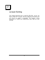
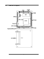
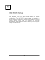
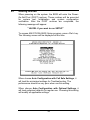
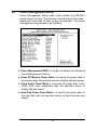
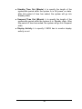
PM-1041 Ver 1.x
486 DX66 with
SVGA CPU Board
@Copyright 1999
All Rights Reserved.
Manual first edition November. 15,1999
The information in this document is subject to change without prior notice in
order to improve reliability, design and function and does not represent a
commitment on the part of the manufacturer.
In no event will the manufacturer be liable for direct, indirect, special,
incidental, or consequential damages arising out of the use or inability to use
the product or documentation, even if advised of the possibility of such
damages.
This document contains proprietary information protected by copyright. All
rights are reserved. No part of this manual may be reproduced by any
mechanical, electronic, or other means in any form without prior written
permission of the manufacturer.
Trademarks
PM-1041 is registered trademark. IBM PC is a
registered trademark of International Business Machines Corporation. Intel is
a registered trademark of Intel Corporation. AMI is registered trademarks of
American Megatrends, Inc. Other product names mentioned herein are used
for identification purposes only and may be trademarks and/or registered
trademarks of their respective companies.
Contents
Contents ........................................................................1
1. Introduction ...............................................................3
1.1
Specifications ..............................................................................4
1.2
What You Have ...........................................................................5
2. Jumper Setting .........................................................6
2.1
PM-1041's Layout........................................................................7
2.2
Unpacking Precautions ................................................................8
2.3
Clear CMOS Setup (JP1) .............................................................9
2.4
DiskOnChip™ Flash Disk (JP2).................................................10
3. Connection..............................................................11
3.1
Floppy Disk Drive Connector (CN1)..........................................12
3.2
IDE Disk Drive Connector (CN4)..............................................13
3.3
Switches, Indicators and IrDA infrared port (JP3)......................14
3.4
Parallel Port (CN5)....................................................................15
3.5
Serial Port (CN2, CN3) .............................................................16
3.6
External Power Connector (CN6) ..............................................17
3.7
VGA Connector (CN7)..............................................................18
3.8
CPU Fan Connector (CN8) ........................................................19
3.9
PC/104 Connection Bus (CN9, CN10) .......................................20
1
3.10 PS/2 Mouse and Keyboard Connector (CN11) ...........................21
3.11 SO-DIMM Socket Connector (CN12) ........................................22
4. AMI BIOS Setup .....................................................23
4.1
Getting Started ..........................................................................24
4.2
Standard CMOS Setup...............................................................25
4.3
Advanced CMOS Setup .............................................................26
4.4
Advanced Chipset Setup ............................................................28
4.5
Power Management Setup .........................................................29
4.6
Peripheral Setup ........................................................................31
5. E2 Key™ Function..................................................33
Appendix A. Watch-Dog Timer .................................35
Appendix B. I/O Information ......................................37
2
1
Introduction
Welcome to the PM-1041 486 DX66 with SVGA CPU Board.
The PM-1041 board is an all-in-one CPU board, which comes
equipped with PC/104 solution for limited-space application. It
offers all the functions that a full-fledged computer needs.
In addition, the PM-1041 provides SVGA display controller on
board, which can supply CRT resolutions up to 1024x768@64K
colors.
This board has a built-in DiskOnChip™(DOC) Flash Disk Socket
for embedded applications. The DOC Flash Disk is 100%
software compatible with hard disk. Users can use any DOS
command without any extra software utility. The DOC is
currently available from 2MB to 144MB.
3
1.1
Specifications
CPU
System bus
connector
System
memory
Enhanced IDE
Interface
Floppy disk
drive interface
Embedded SGS Thomson DX-66 STPC Client
PC104 connector
One 144-pin SODIMM socket supports 8,16 or 32MB
EDO/FPR DRAM
Supports up to two EIDE devices with BIOS auto-detect
function
Supports up to two floppy disk drives
Serial ports
Two RS-232 ports with 16C550 UART (or compatible)
with 16-byte FIFO buffer. Support up to 115.2Kbps.
Ports can be individually configured to COM1, COM2 or
disabled.
Bi-directional
parallel Port
Configurable to LPT1, LPT2, LPT3 or disabled. Supports
EPP/ECP/SPP.
IrDA port
Supports Serial Infrared (SIR) and Amplitude Shift
Keyed IR (ASKIR) interface
Watch-dog
timer
Can be set by 1~255 seconds intervals. Reset or NMI is
generated when CPU does not periodically trigger the
timer.
VGA display
Completes backward compatibility to VGA and SVGA ,
supports CRT resolutions up to 1024 x 768 @ 64K
colors , 512KB – 4MB share memory , set in BIOS
Flash disk
socket
The DiskOnChip™ compatible 32-pin dip socket is
provided for Flash Disk (DiskOnChip™ ) applications
which will let users to use the Flash Disk with DOS
command without any extra software utility.
Keyboard /
Mouse
connector
Power
consumption
Operating
temperature
Supports standard PC/AT keyboard and PS/2 mouse
+5V @1.4A
0° ~ 55°C ( CPU needs Cooler)
4
1.2
What You Have
In addition to this User's Manual, the PM-1041 package includes
the following items:
•
PM-1041 486DX66 with SVGA CPU board
•
RS-232 cable x 2
•
Printer cable x 1
•
FDD cable x 1
•
HDD cable x 1
•
One 6-pin header converts to two 6-pin DIN cable for keyboard
and mouse connection x 1
•
VGA cable x 1
If any of these items are missing or damaged, contact the dealer
from whom you purchased this product. Keep the shipping
materials and carton in case you want to ship or store the
product in the future.
5
2
Jumper Setting
This chapter describes how to install the PM-1041. At first, the
layout of PM-1041 is shown, and the unpacking information that
you should be careful is described. The jumpers setting
instructions of CMOS and DiskOnChip Flash Disk are also
included.
6
2.1
PM-1041's Layout
7
2.2
Unpacking Precautions
Some components on PM-1041 SBC are very sensitive to static
electric charges and can be damaged by a sudden rush of power.
To protect it from unintended damage, be sure to follow these
precautions:
ü
Ground yourself to remove any static charge before touching
your PM-1041 SBC. You can do it by using a grounded wrist
strap at all times or by frequently touching any conducting
materials that is connected to the ground.
ü
Handle your PM-1041 SBC by its edges. Don’t touch IC chips,
leads or circuitry if not necessary.
ü
Do not plug any connector or jumper while the power is on.
8
2.3
Clear CMOS Setup (JP1)
If you want to clear the CMOS Setup (for example: if you forgot
the password, you should clear the setup and then set the
password again.), you should close the JP1 about 3 seconds,
then open again. Now, the password has been cleared from
your CMOS.
1
2
3
JP1 : Clear CMOS Setup
• JP1 : Clear CMOS Setup (Reserve Function)
JP1
DESCRIPTION
1-2
NORMAL
2-3
CLR CMOS
9
2.4
DiskOnChip™ Flash Disk (JP2)
The DiskOnChip™ Flash Disk Chip (DOC) is produced by M
Systems. Because the DOC is 100% software compatible to
hard disk and DOS, users don‘t need any extra software utility. It
is just “plug and play”, easy and reliable. Right now the DOC is
available from 2MB to 144MB. The DiskOnChip will only share
8KB memory address.
5
3
1
6
4
2
JP2 : DiskOnChip Flash Disk Setup
• JP2 : DiskOnChip Memory Address Setting
JP2
Address
1-2
3-4
5-6
C8000 – C9FFF
OPEN CLOSE CLOSE
CLOSE OPEN CLOSE
D0000 – D1FFF
OPEN
OPEN CLOSE
D8000 – D9FFF
10
3
Connection
This chapter describes how to connect peripherals, switches and
indicators to the PM-1041 board.
Table of Connectors
LABEL
CN1
CN2
CN3
CN4
CN5
CN6
CN7
CN8
CN9
CN10
CN11
CN12
FUNCTION
Floppy Disk Drive Connector
COMA Connector
COMB Connector
IDE Disk Drive Connector
Parallel Port
External Power Connector
VGA Connector
CPU Fan Connector
PC/104-64 CON A
PC/104-40 CON B
PS/2 Mouse and Keyboard Connector
SO-DIMM Socket Connector
11
- 1
- 3
- 5
- 7
- 9
- 11
- 13
- 15
- 17
- 19
- 21
- 23
- 25
- 27
- 29
- 31
- 33
2 - REDUCE WRITE
4 - NC
6 - NC
8 - INDEX#
10 - MOTOR ENABLE A#
12 - DRIVE SELECT B#
14 - DRIVE SELECT A#
16 - MOTOR ENABLE B#
18 - DIRECTION#
20 - STEP#
22 - WRITE DATA#
24 - WRITE GATE#
26 - TRACK 0#
28 - WRITE PROTECT#
30 - READ DATA#
32 - SIDE 1 SELECT#
34 - DISK CHANGE#
3.1
Floppy Disk Drive Connector (CN1)
The PM-1041 board comes equipped with a 34-pin daisy-chain
drive connector cable which can support up to two floppy drives.
The detailed pin assignment of the connector is specified as
below:
GND
CN1 : FDC Connector
12
3.2
IDE Disk Drive Connector (CN4)
You can attach four IDE (Integrated Device Electronics) hard
disk drives to the PM-1041 IDE controller. The IDE supports the
Ultra DMA/33 interface.
RESET# - 1
DATA 7 - 3
DATA 6 - 5
DATA 5 - 7
DATA 4 - 9
DATA 3 - 11
DATA 2 - 13
DATA 1 - 15
DATA 0 - 17
GND - 19
IDE DRQ - 21
IOW# - 23
IOR# - 25
IDE CHRDY - 27
IDE DACK - 29
INTERRUPT -31
SA1 - 33
SA0 - 35
HDC CS0# - 37
HDD ACTIVE# - 39
VCC - 41
GND - 43
2 - GND
4 - DATA8
6 - DATA9
8 - DATA10
10 - DATA11
12 - DATA12
14 - DATA13
16 - DATA14
18 - DATA15
20 - NC
22 - GND
24 - GND
26 - GND
28 - GND
30 - GND - DEFAULT
32 - NC
34 - NC
36 - SA2
38 - HDE CS1#
40 - GND
42 - NC
44 - NC
CN4 : HDD Connector
13
3.3
Switches, Indicators and IrDA infrared port (JP3)
The connection of JP3 is illustrated as the following table for
reference.
1
2
15 16
• JP3: General connectors
PIN NO.
BATTERY
CON
RESET
HDDLED
WATCH
DOG
1
3
5
7
9
11
13
15
DESCRIPTION
BATTERY
VCC
GND
RESET SW
VCC
IDE LED
Watch dog active
Reset in
PIN NO.
2
4
6
8
10
12
14
16
DESCRIPTION
VCC
NC
IR-RX
GND
IR-TX
NC
KEYLOCK
GND
IR
CONNECTOR
KEYLOCK
CON
Note : JP3 Pin 13&15 Watch-Dog Setting
JP1
Shut
Open
Watch-Dog Setting
Enabled
Disabled
For detailed information on Watch-Dog Timer, please refer to
Appendix A.
14
3.4
Parallel Port (CN5)
This port is usually connected to a printer. The PM-1041
includes an on-board parallel port accessed through a 26-pin
mini-pitched flat-cable connector CN5.
NC - 26
GND - 24
GND - 22
GND - 20
GND - 18
INITIALIZE - 16
AUTO FORM FEED# - 14
PAPER EMPTY - 12
ACKNOWLEDGE - 10
DATA 6 - 8
DATA 4 - 6
DATA 2 - 4
DATA 0 - 2
25 - GND
23 - GND
21 - GND
19 - GND
17 - PRINTERSELECT LN#
15 - ERROR#
13 - PRINTER SELECT
11 - BUSY
9 - DATA 7
7 - DATA 5
5 - DATA 3
3 - DATA 1
1 - STROBE#
CN5 : Parallel Port Connector
15
Serial Port (CN2, CN3)
2 - NSIN
4 - NDTR
6 - NDSR
8 - NCTS
10 - NC
The PM-1041 offers two high speed NS16C550 compatible
UARTs with Read/Receive 16 byte FIFO serial ports.
CN3
(COMB)
CN2
(COMA)
NCD - 1
NSOUT - 3
GND - 5
NRTS - 7
NRIA - 9
3.5
NC - 10
NCTS - 8
NDSR - 6
NDTR - 4
NSIN - 2
9 - NRIA
7 - NRTS
5 - GND
3 - NSOUT
1 - NCD
CN2&3 : COMA and COMB Connectors
16
3.6
External Power Connector (CN6)
The PM-1041 has an on-board external power connector CN6.
The PM-1041 is only powered by Vcc(+5) which should come
from external power connector CN6's pin1 and pin8, and power
GND from pin4 and pin5. The extra power supply like ±12VDC
and -5VDC provided by CN6 will be passed to CN9 and CN10
and only for PC104 slot use.
1 - VCC
2 - +12V
3 - -12V
4 - GND
5 - GND
6 - -5V
7 - +12V
8 - VCC
CN6: External Power Connector
17
3.7
VGA Connector (CN7)
PM-1041's built-in 16-pin VGA connector can directly connect to
your CRT monitor via the attached VGA cable.
NC - 16
GND - 14
DDC1 - 12
GND - 10
VSYNC - 8
GND - 6
HSYNC - 4
GND - 2
15 - DDCO
13 - NC
11 - NC
9 - BLUE
7 - GND
5 - GREEN
3 - VCC
1 - RED
CN7: 16-PIN Female Connector
18
3.8
CPU Fan Connector (CN8)
The PM-1041 provides an optional CPU cooling fan connector
which only presents when +12V power is supplied to CN6.
Please note that the PM-1041's STPC chip has already installed
a heat sink.
However, while running under environment
temperature above 60¢ J, users still have to add an additional
CPU cooling fan.
1 - +12V
2 - GNC
CN8: CPU Fan Connector
19
GND - 40
SD15 - 39
SD14 - 38
SD13 - 37
SD12 - 36
SD11 - 35
SD10 - 34
SD9 - 33
SD8 - 32
MEMW - 31
MEMR - 30
LA17 - 29
LA18 - 28
LA19 - 27
LA20 - 26
LA21 - 25
LA22 - 24
LA23 - 23
SBHE - 22
GND - 21
20 - GND
19 - GNC
18 - MASTER#
17 - VCC
16 - DRQ7
15 - DACK7#
14 - DRQ6
13 - DACK6#
12 - DRQ5
11 - DACK5#
10 - DRQ0
9 - DACK0#
8 - IRQ14
7 - IRQ15
6 - IRQ12
5 - IRQ11
4 - IRQ10
3 - IOCS16
2 - MCS16
1 - GND
IOCHCK# - 1
SD7 - 2
SD6 - 3
SD5 - 4
SD4 - 5
SD3 - 6
SD2 - 7
SD1 - 8
SD0 - 9
IOCHRDY - 10
AEN - 11
LA19 - 12
LA18 - 13
LA17 - 14
SA16 - 15
SA15 - 16
SA14 - 17
SA13 - 18
SA12 - 19
SA11 - 20
SA10 - 21
SA9 - 22
SA8 - 23
SA7 - 24
SA6 - 25
SA5 - 26
SA4 - 27
SA3 - 28
SA2 - 29
SA1 - 30
SA0 - 31
GND - 32
33 - GND
34 - RSTDRV
35 - VCC
36 - IRQ9
37 - -5V
38 - DRQ2
39 - -12V
40 - ZWS
41 - +12V
42 - GND
43 - SMEMW#
44 - SMEMR#
45 - IOW#
46 - IOR#
47 - DACK3#
48 - DRQ3
49 - DACK1#
50 - DRQ1
51 - REFRESH#
52 - ISASYSCLK
53 - IRQ7
54 - IRQ6
55 - IRQ5
56 - IRQ4
57 - IRQ3
58 - DACK2
59 - TC
60 - ALE
61 - VCC
62 - OSC
63 - GND
64 - GND
3.9
PC/104 Connection Bus (CN9, CN10)
The PM-1041's PC/104 expansion bus lets you attach any kind
of PC/104 modules. There are two PC/104 connectors on this
board: PC/104-64 and PC/104-40.
CN9 : PC/104-64 CON A
CN10 : PC/104-64 CON B
20
PS/2 Mouse and Keyboard Connector (CN11)
The attached 6-pin header converting to two 6-pin DIN cables for
keyboard and mouse connection allows users to connect both
PS/2 mouse and keyboard. Please note that only by connecting
with the attached cable, the keyboard and mouse will work
appropriately.
1 - KEYBOARD DATA
2 - MOUSE DATA
3 - GND
4 - VCC
5 - DEYBOARD CLOCK
6 - MOUSE CLOCK
3.10
CN11 : PS/2 Mouse and Keyboard Connector
21
3.11
SO-DIMM Socket Connector (CN12)
144
143
CN12 : SO-DIMM Socket Connector
1
2
3
4
5
6
7
8
9
10
11
12
13
14
15
16
17
18
19
20
21
22
23
24
25
26
27
28
29
GND
GND
MD0
MD32
MD1
MD33
MD2
MD34
MD3
MD35
+3.3V
+3.3V
MD4
MD36
MD5
MD37
MD6
MD38
MD7
MD39
GND
GND
CAS0
CAS4
CAS1
CAS5
+3.3V
+3.3V
MA0
30
31
32
33
34
35
36
37
38
39
40
41
42
43
44
45
46
47
48
49
50
51
52
53
54
55
56
57
58
MA3
MA1
MA4
MA2
MA5
GND
GND
MD8
MD40
MD9
MD41
MD10
MD42
MD11
MD43
+3.3V
+3.3V
MD12
MD44
MD13
MD45
MD14
MD46
MD15
MD47
GND
GND
NC
NC
59
60
61
62
63
64
65
66
67
68
69
70
71
72
73
74
75
76
77
78
79
80
81
82
83
84
85
86
87
NC
NC
NC
NC
+3.3V
+3.3V
NC
NC
MWE
NC
RAS0
NC
NC
NC
GND
NC
GND
GND
NC
NC
NC
NC
GND
GND
MD16
MD48
MD17
MD49
MD18
22
88
89
90
91
92
93
94
95
96
97
98
99
100
101
102
103
104
105
106
107
108
109
110
111
112
113
114
115
116
MD50
MD19
MD51
GND
GND
MD20
MD52
MD21
MD53
MD22
MD54
MD23
MD55
+3.3V
+3.3V
MA6
MA7
MA8
MA11
GND
GND
MA9
NC
MA10
NC
+3.3V
+3.3V
CAS2
CAS6
117
118
119
120
121
122
123
124
125
126
127
128
129
130
131
132
133
134
135
136
137
138
139
140
141
142
143
144
CAS3
CAS7
GND
GND
MD24
MD56
MD25
MD57
MD26
MD58
MD27
MD59
+3.3V
+3.3V
MD28
MD60
MD29
MD61
MD30
MD62
MD31
MD63
GND
GND
NC
NC
+3.3V
+3.3V
4
AMI BIOS Setup
The PM-1041 uses the AMI PCI/ISA BIOS for system
configuration. The AMI BIOS setup program is designed to
provide maximum flexibility in configuring the system by offering
various options which may be selected for end-user
requirements. This chapter is written to assist you in the proper
usage of these features.
23
4.1
Getting Started
When powering on the system, the BIOS will enter the PowerOn-Self-Test (POST) routines. These routines will be executed
for system test, initialization and system configuration
verification. After the POST routines are completed, the
following message will appear:
" Hit DEL if you want to run SETUP"
To access AMI PCI/ISA BIOS Setup program, press <Del> key.
The following screen will be displayed at this time.
When choose Auto Configuration with Fail Safe Settings, it
will load the minimized settings for Troubleshooting. The
performance should be very poor when use this setting.
When choose Auto Configuration with Optimal Settings, it
will load optimized defaults for regular use. Choosing this setting
will modify all applicable settings.
24
4.2
Standard CMOS Setup
The Standard CMOS Setup is used for basic hardware system
configuration. The main function is for Date/Time setting and
Floppy/Hard Disk Drive setting. Please refer to the following
screen for this setup.
For IDE hard disk drive setup, please check the following setup
procedure:
1. Use the Auto setting for detection during boot up.
2. Use the IDE HDD AUTO DETECTION in the main menu to
automatically enter the drive specifications.
3. Manually enter the specifications by yourself from
the ”User“ option.
25
4.3
Advanced CMOS Setup
The Advanced CMOS Setup is designed for user's tuning best
performance of the PM-1041 board. As for normal operation,
users don‘t have to change any default setting. The default
setting is pre-set for most reliable operation.
Users can set “System Keyboard” to “Absent “ for the
applications which don't need keyboard.
You can change the value of each option by using <PgUp> and
<PgDn> key. The available values are shown on the right screen.
l
Quick Boot > Enabled: this will enable the BIOS to boot
quickly when you turn on your computer. The BIOS will only
check the first 1MB of the system memory.
l
Quick Boot > Disabled: the BIOS will test all system memory
when it boots up. It will spend about 40 seconds until it
receives a Ready signal from the HDD. It will also wait for you
to press the <Del> key or not.
l
1st, 2nd, 3rd Boot Device > to define the device type for
booting after the routines check up completes. If the 1st Boot
Device fails, the BIOS will attempt to boot from the 2nd or the
3rd device.
26
l
Try Other Boot Devices > the BIOS will try to boot from any
other available device in the system if the 1st, 2nd and 3rd
device fails to boot.
l
BootUp Num-Lock > to turn on/off the Num-Lock option on a
enhanced keyboard when you boot. If you turn it off, the arrow
keys on the numeric keypad can be used just as the other set
of arrow keys on the keyboard and vice versa.
l
PS/2 Mouse Support > to testify whether or not a PS/2 mouse
is supported.
l
System Keyboard > to testify whether or not a keyboard is
attached to the computer.
l
Password Check > to define if a password is necessary or not
for access to the system.
l
Boot to OS/2 > if you run the OS/2 operating system, this
option must be set to yes.
l
System BIOS Cacheable > to define whether or not the
memory segment FOOOH can be read from or written to cache
memory. Setting it Enabled will give faster execution in your
system.
l
XXXX, 16k Shadow > ROM Shadow is a technique in which
BIOS code is copied from slower ROM to faster RAM. If you
enable it then the BIOS will be executed from the RAM. Each
option allows 16KB segment to be shadowed to the RAM.
27
4.4
Advanced Chipset Setup
These setup functions mainly work for Chipset. These options
are used to change the Chipset‘s registers. Please carefully
change any default setting, otherwise the system may become
unstable.
l
Memory Hole at 15M-16M > to specify the location of a
memory hole in the CMOS RAM. This setting reserves 15MB
to 16 MB memory address space for ISA expansion cards that
specifically require this setting. Memory from 15MB and up will
be unavailable to the system because expansion cards can
only access memory up to 16MB.
l
VGA Frame Buffer Size (KB) > to specify VGA share memory
size
28
4.5
Power Management Setup
Power Management Setup helps users handle the PM-1041
board‘s “green” function. The features could shut down the video
display and hard disk to save energy for example. The power
management setup screen is as following:
l
Power Management/APM > to enable or disable the Advanced
Power Management feature.
l
Green PC Monitor Power State > to specify the power state of
the monitor after the specified period of display-idle has ended.
l
Video Power Down Mode > to specify the power state of the
VESA VGA video subsystem after the specified period of
display-idle has ended.
l
Hard Disk Power Down Mode > to specify the power state of
the hard disk after the specified period of hard drive-idle has
ended.
29
l
Standby Time Out (Minute) > to specify the length of the
system-idle period while the system is in full power on state.
After this period of time has ended, the system will go into
Standby state.
l
Suspend Time Out (Minute) > to specify the length of the
system-idle period while the system is in Standby state. After
this period of time has ended, the system will go into Suspend
state.
l
Display Activity > to specify if BIOS has to monitor display
activity or not.
30
4.6
Peripheral Setup
This setup works mostly on (is almost working for) Multi-I/O Chip
(W83977F). The options are used to change the Chipset‘s
registers. Please carefully change any default setting to meet
your application needs perfectly. The only special concern is
Onboard Serial Port B. If you are using the IrDA port, you have
to set this port accordingly.
When you enter the Peripheral Setup, the following items are
available for setting:
l
On-board FDC > The floppy disk drive controller can be
Enabled or Disabled by this item. When you do not need floppy
disk, the FDD controller can be disabled. If you set it Auto, the
BIOS will try to enable any floppy drive controller on the ISA
Bus.
l
Serial Port A > The options are Disable, 3F8, 2F8, 3E8, 2E8
and Auto. You can set the I/O address of the serial port A
(COMA) or disable it.
l
Serial Port B > The options are Disable, 3F8, 2F8, 3E8, 2E8
and Auto. You can set the I/O address of the serial port B
(COMB) or disable it.
31
l
OnBoard Parallel Port > The options are Auto, Disable, 3BC,
378 or 278. You can set the I/O address of the parallel port or
disable it.
l
IR Port Support > to specify the IO Port address of the IR Port
l
Parallel Port Mode > PM-1041 provides EPP Mode. EPP
passes the parallel port to be used with devices which stick to
the EPP specification. The existing parallel port signals will be
used by EPP to provide asymmetric bi-directional data transfer
driven by the host devices.
l
Parallel Port IRQ > to define the Interrupt Request (IRQ) which
is used by the parallel port.
l
Parallel Port DMA Channel > to set the DMA Channel used by
the parallel port.
32
5
2
E Key™ Function
2
The PM-1041 provides an outstanding E KEY™ function for
2
system integrator. Based on the E KEY™ you are free to store
the ID Code, Pass Word, or Critical Data in the 1Kbit EEPROM.
Because the EEPROM is nonvolatile memory, you don’t have to
worry about the loss of the very important data.
2
Basically the E KEY™ is based on a 1Kbit EEPROM which is
configured to 64 words (from 0 to 63). You could access (read or
write) each word at any time.
2
When you start to use the E KEY™ you should have the ut
ility in
the package. The software utility will include four files as follows:
README.DOC
E2KEY.OBJ
EKEYDEMO.C
EKEYDEMO.EXE.
The E2KEY.OBJ provides two library functions for users to
2
integrate their applications with E KEY™ function. Theselibrary
functions (read_e2key and write_e2key) are written and
compiled by C Language. Please check the following statement,
then you will understand how to implement it easily.
Editor Note: What do these "/*" marks in pairs stand for?
33
unsigned int read_e2key(unsigned int address)
2
/* This function will return the E KEY™’s data at address. The
address range is from 0 to 63. Return data is one word, 16 bits */
void write_e2key(unsigned int address,unsigned data)
2
/* This function will write the given data to E KEY™ at address.
The address range is from 0 to 63. The data value is from 0 to
0xffff. */
To easy start to use the function, please refer to the included
EKEYDEMO.C code at first.
2
Please note the E KEY™ function is based on the working of
parallel port. Therefore you should enable the ROCKYP288EV’s parallel p ort, otherwise it will not be working.
34
Appendix A. Watch-Dog Timer
The Watch-Dog Timer is provided to ensure that stand-alone
systems can always recover from catastrophic conditions that
cause the CPU to crash. This condition may have occurred by
external EMI or a software bug. When the CPU stops working
correctly, hardware on the board will perform hardware reset
(cold boot) to bring the system back to a known state.
The Watch-Dog Timer is controlled by three I/O ports.
443
443
(hex)
843
(hex)
Write
Read
Read
Set Watch-Dog Time period
Enable the refresh the Watch-Dog
Timer.
Disable the Watch-Dog Timer.
To enable the Watch-Dog Timer, users have to define the Timer
before enable the Watch-dog Timer function. The output data is
a value of time interval and the range of the value is from
01(hex) to FF(hex) and time interval 1 sec to 255 sec.
Data
01
02
03
04
.
.
.
FF
Time Interval
1 sec
2 sec
3 sec
4 sec
.
.
.
255 sec
This will enable and activate the countdown timer which will
eventually time out and reset the CPU to ensure that this reset
condition does not occur, the Watch-Dog Timer must be
periodically refreshed by reading the same I/O ports 843H and
443H. This must be done within the time out period that is
selected by software, please refer to the example program.
35
A tolerance of at least 30% must be maintained to avoid
unknown routines within the operating system (DOS), such as
disk I/O that can be very time consuming. Therefore if the time
out period has been set to 10 seconds, the I/O port 443H must
be read within 7 seconds.
Note: when exiting a program, it is necessary to disable the
Watch-Dog Timer, otherwise the system will reset.
Example program:
TIMER_PORT = 443H
TIMER_START = 443H
TIMER_STOP = 843H
;
; INITIAL TIME PERIOD COUNTER
;
MOV DX, TIME_PORT
OUT AL, 8 ; 8 SECONDS
;
; ADD YOUR APPLICATION HERE
;
MOV DX, TIMER_START
IN
AL, DX.
; START COUNTER
;
; ADD YOUR APPLICATION HERE
;
W_LOOP:
MOV DX,TIMER_STOP
IN
AL,DX
MOV DX, TIMER_START
IN
AL, DX.
; RESTART COUNTER
;
; ADD YOUR APPLICATION HERE
;
CMP
EXIT_AP, 0
JNE
W_LOOP
MOV DX, TIMER_STOP
IN
AL, DX
;
; EXIT AP
;
36
Appendix B. I/O Information
IO Address Map
I/O Address Range
000-01F
020-021
040-05F
060-06F
070-07F
080-09F
0A0-0BF
0C0-0DF
0F0
0F1
0F2
0F8-0FF
1F0-1F8
200-207
278-27F
2E8-2EF
2F8-2FF
300-31F
360-36F
378-37F
3B0-3BF
3C0-3CF
3D0-3DF
3E8-3EF
3F0-3F7
3F8-3FF
443
843 or 043
Description
DMA Controller #1
Interrupt Controller #1, Master
8254 timer
8042 (Keyboard Controller)
Real time Clock, NMI (non-maskable interrupt)
Mask
DMA Page Register
Interrupt Controller #2
DMA Controller #2
Clear Math Coprocessor Busy
Reset Math Coprocessor
Core logic programming configuration
Math Coprocessor
Fixed Disk
Game I/O
Parallel Printer Port 2 (LPT3)
Serial Port 4
Serial Port 2
Prototype Card
Reserved
Parallel Printer Port 1 (LPT2)
Monochrome Display and Printer Adapter (LPT1)
Reserved
Color/Graphics Monitor Adapter
Serial Port 3
Diskette Controller
Serial Port 1
Watch-dog timer enable
Watch-dog timer disable
37
1st MB Memory Address Map
Memory address
00000-9FFFF
A0000-BFFFF
C0000-C7FFF
*D6000-DDFFF
F0000-FFFFF
1000000-
Description
System memory
VGA buffer
VGA BIOS
DOC 2000
System BIOS
Extend BIOS
IRQ Mapping Chart
IRQ0
IRQ1
IRQ2
IRQ3
IRQ4
IRQ5
IRQ6
IRQ7
System Timer
Keyboard
Cascade to IRQ Controller
COM2
COM1
Unused
FDC
Printer
IRQ8
IRQ9
IRQ10
IRQ11
IRQ12
IRQ13
IRQ14
IRQ15
RTC Clock
Unused
Unused
Unused
PS/2 mouse
FPU
Primary IDE
Secondary IDE
DMA Channel Assignments
DMA Channel
0
1
2
3
4
5
6
7
Function
Available
Available
Floppy Disk (8-bit transfer)
Available
Cascade for DMA controller 1
Available
Available
Available
38