1
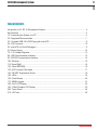
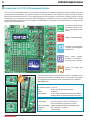
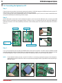
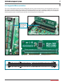
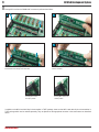
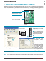
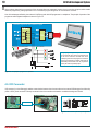
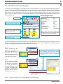
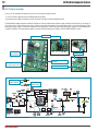
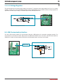
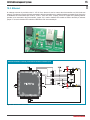
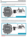
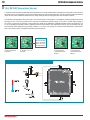
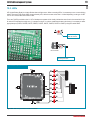
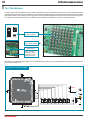
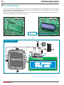
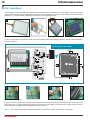
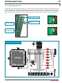
All MikroElektronika´s development systems represent irreplaceable tools for
programming and developing microcontroller-based devices. Carefully chosen
components and the use of machines of the last generation for mounting and
testing thereof are the best guarantee of high reliability of our devices. Due to
simple design, a large number of add-on modules and ready to use examples,
all our users, regardless of their experience, have the possibility to develop
their project in a fast and efficient way.
User manual
Development System
If you have any questions, comments or business proposals, do not hesitate to contact us at [email protected]
If you are experiencing some problems with any of our products or just need additional information, please place your ticket at
www.mikroe.com/en/support
If you want to learn more about our products, please visit our website at www.mikroe.com
LV 18F v6
™
DISCLAIMER
All the products owned by MikroElektronika are protected by copyright law and international copyright treaty.
Therefore, this manual is to be treated as any other copyright material. No part of this manual, including
product and software described herein, may be reproduced, stored in a retrieval system, translated or
transmitted in any form or by any means, without the prior written permission of MikroElektronika. The
manual PDF edition can be printed for private or local use, but not for distribution. Any modification of this
manual is prohibited.
TO OUR VALUED CUSTOMERS
I want to express my thanks to you for being interested in our products and for having confidence in
mikroElektronika.
The primary aim of our company is to design and produce high quality electronic products and to constantly
improve the performance thereof in order to better suit your needs.
Nebojsa Matic
General Manager
MikroElektronika provides this manual ‘as is’ without warranty of any kind, either expressed or implied,
including, but not limited to, the implied warranties or conditions of merchantability or fitness for a particular
purpose.
MikroElektronika shall assume no responsibility or liability for any errors, omissions and inaccuracies that may
appear in this manual. In no event shall MikroElektronika, its directors, officers, employees or distributors be
liable for any indirect, specific, incidental or consequential damages (including damages for loss of business
profits and business information, business interruption or any other pecuniary loss) arising out of the use
of this manual or product, even if MikroElektronika has been advised of the possibility of such damages.
MikroElektronika reserves the right to change information contained in this manual at any time without prior
notice, if necessary.
HIGH RISK ACTIVITIES
The products of MikroElektronika are not fault – tolerant nor designed, manufactured or intended for use or
resale as on – line control equipment in hazardous environments requiring fail – safe performance, such as
in the operation of nuclear facilities, aircraft navigation or communication systems, air traffic control, direct
life support machines or weapons systems in which the failure of Software could lead directly to death,
personal injury or severe physical or environmental damage (‘High Risk Activities’). MikroElektronika and its
suppliers specifically disclaim any expressed or implied warranty of fitness for High Risk Activities.
TRADEMARKS
The Mikroelektronika name and logo, the Mikroelektronika logo, mikroC, mikroC PRO, mikroBasic, mikroBasic PRO, mikroPascal, mikroPascal PRO, AVRflash, PICflash, dsPICprog, 18FJprog, PSOCprog, AVRprog, 8051prog, ARMflash, EasyPIC5, EasyPIC6, BigPIC5, BigPIC6, dsPIC PRO4, Easy8051B, EasyARM,
EasyAVR5, EasyAVR6, BigAVR2, EasydsPIC4A, EasyPSoC4, EasyVR Stamp LV18FJ, LV24-33A, LV32MX,
PIC32MX4 MultiMedia Board, PICPLC16, PICPLC8 PICPLC4, SmartGSM/GPRS, UNI-DS are trademarks
of Mikroelektronika. All other trademarks mentioned herein are property of their respective companies.
All other product and corporate names appearing in this manual may or may not be registered trademarks
or copyrights of their respective companies, and are only used for identification or explanation and to the
owners’ benefit, with no intent to infringe.
The Microchip name and logo, the Microchip logo, Accuron, dsPIC, KeeLoq, microID, MPLAB, PIC, PICmicro, PICSTART, PRO MATE,
PowerSmart, rfPIC and SmartShunt are registered trademarks of Microchip Technology Incorporated in the U.S.A and other countries.
©MikroelektronikaTM, 2009, All Rights Reserved.
3
page
LV 18F v6 Development System
TABLE OF CONTENTS
Introduction to LV 18F v6 Development System .............................................................................. 4
Key Features .................................................................................................................................... 5
1.0. Connecting the System to a PC ................................................................................................ 6
2.0. Supported Microcontrollers ........................................................................................................ 7
3.0. On-board USB 2.0 LV18PICprog with mikroICD ...................................................................... 9
4.0. ICD Connector .......................................................................................................................... 10
5.0. mikroICD (In-Circuit Debugger) ................................................................................................. 11
6.0. Power Supply ............................................................................................................................ 12
7.0. 3.3V Voltage Regulator ............................................................................................................. 13
8.0. USB Communication Interface ................................................................................................. 13
9.0. RS-232 Communication Interface ............................................................................................ 14
10.0. Ethernet .................................................................................................................................. 15
11.0. Serial RAM .............................................................................................................................. 16
12.0. Serial EEPROM ...................................................................................................................... 16
13.0. A/D Converter Test Inputs ....................................................................................................... 17
14.0. DS1820 Temperature Sensor ................................................................................................. 18
15.0. LEDs ....................................................................................................................................... 19
16.0. Push Buttons ........................................................................................................................... 20
17.0. MENU Keypad ........................................................................................................................ 21
18.0. 2x16 LCD Display ................................................................................................................... 22
19.0. 128x64 Graphic LCD Display .................................................................................................. 23
20.0. Touch Panel ............................................................................................................................ 24
21.0. I/O Ports .................................................................................................................................. 25
MikroElektronika
page
4
LV 18F v6 Development System
Introduction to LV 18F v6 Development System
The LV 18F v6™ development system is an extraordinary development tool suitable for programming and experimenting with PIC®
microcontrollers from Microchip®. The system includes an on-board programmer with mikroICD™ support providing an interface
between the microcontroller and a PC. You are simply expected to write a program in one of the PIC compilers, generate a .hex file
and program your microcontroller using the on-board LV18PICprog™ programmer. Numerous on-board modules, such as 128x64
graphic LCD display, alphanumeric 2x16 LCD display, serial EEPROM etc, are provided on the board and allow you to easily simulate
the operation of the target device.
Full-featured and user-friendly
development system for PIC
18Fxx microcontroller based
devices
USB 2.0 on-board programmer
Hardware In-Circuit Debugger
for step by step debugging at
hardware level
Bult-in voltage regulator
providing 3.3V required for
the microcontroller operation
Graphic LCD display with
backlight
The LV18PICflash program for programming provides a complete list of all
supported microcontrollers. The latest version of this program with updated
list of supported microcontrollers can be downloaded from our website at
www.mikroe.com
Package contains:
Development System: LV 18F v6
CD:
product CD with appropriate software
Cables:
USB cable
Documentation:
LV 18F v6 and LV18PICFlash manuals, quick guide for
installing USB drivers, electrical schematic of the system
System specification:
Power supply:
over a DC connector (7-23V AC or 9-32V DC); or
over a USB cable for programming (5V DC)
Power consumption: 40mA in idle state when all on-board modules are off
Dimension:
26,5 x 22cm (10,4 x 8,6inch)
Weight:
~404g (0.89lbs)
MikroElektronika
5
1
2
3
4
5
6
7
8
9
page
LV 18F v6 Development System
10
30
11
29
28
12
13
27
14
26
15
25
16
24
23
22 21
20
Key Features
1.
2.
3.
4.
5.
6.
7.
8.
9.
10.
11.
12.
13.
14.
On-board programmer’s USB connector
Connector for Microchip’s debugger (ICD2 or ICD3)
Ethernet module
USB communication interface
A connector for RS-232 communication
A/D converter test inputs
B connector for RS-232 communication
DIMM-168P connector for MCU card
Pull-up/pull-down resistor selection
DIP switch enables pull-up/pull-down resistors
I/O port connectors
DIP switch turns on/off integrated modules
DS1820 temperature sensor
Serial RAM
19
18
17
15. Serial EEPROM
16. Graphic LCD display contrast adjustment
17. Touch panel controller
18. Graphic LCD display connector
19. Touch panel connector
20. Push buttons simulate digital inputs
21. Shorting jumper for protective resistor
22. Selector for pins’ logic state
23. Reset button
24. MENU keypad
25. 3.3V voltage regulator
26. Power supply voltage regulator
27. 70 LEDs indicate pins’ logic state
28. Alphanumeric LCD display contrast adjustment
29. Alphanumeric LCD display connector
30. USB 2.0 with mikroICD support programmer
MikroElektronika
page
6
LV 18F v6 Development System
1.0. Connecting the System to a PC
Step 1:
Follow the instructions provided in the relevant manuals and install the LV18PICflash program and USB drivers from the product CD.
USB drivers are necessary for the proper operation of the on-board programmer.
In case you already have some of the MikroElektronika’s PIC compilers installed on your PC, there is no need to reinstall USB drivers
as they will automatically be installed along with the compiler.
Step 2:
Use the USB cable to connect the LV 18F v6 development system to a PC. One end of the USB cable, with a connector of the USB
B type, should be connected to the development system, as shown in Figure 1-2, whereas the other end of the cable (USB A type)
should be connected to a PC. When establishing a connection, make sure that jumper J10 is placed in the USB position as shown in
Figure 1-1.
DC connector
USB connector
1
2
J10 power supply
selector
POWER SUPPLY switch
Figure 1-1: Power supply
Figure 1-2: Connecting USB cable
Step 3:
Turn on your development system by setting the POWER SUPPLY switch to the ON position. Two LEDs marked as POWER and USB
LINK will automatically illuminate indicating that your development system is ready to use. Use the on-board programmer and the
LV18PICflash program to dump a code into the microcontroller and employ the system to test and develop your projects.
NOTE:
If some additional modules are used, such as LCD, GLCD etc, it is necessary to place them properly on the development
system while it is turned off. Otherwise, either can be permanently damaged. Refer to Figure below for the proper placing of
additional modules.
Figure 1-3 : Placing additional modules on the board
MikroElektronika
7
page
LV 18F v6 Development System
2.0. Supported Microcontrollers
The LV 18F v6 development system provides a DIMM-168P connector to place an MCU card into. Such development system comes
with an MCU card with an 80-pin microcontroller in TQFP package soldered on it, Figure 2-3. Besides, the MCU card alone provides
an oscillator as well as 80 soldering pads connected to microcontroller pins. Each pad is marked same as the pin it is connected to.
Soldering pads also make connection between the MCU card and target device’s modules easy.
DIMM-168P connector
for placing MCU card
with microcontroller in
TQFP package
Figure 2-2: DIMM-168P connector with MCU card placed
Figure 2-1: DIMM-168P connector
Figure 2-3: MCU card with 80-pin microcontroller in TQFP package soldered on it
Figure 2-4: Schematic of the DIMM-168P connector’s pinout
MikroElektronika
page
8
LV 18F v6 Development System
Placing MCU card into the DIMM-168P connector is performed as follows:
1
A
2
B
Open extraction levers A and B
Place the MCU card into the DIMM-168P connector
4
3
Push the MCU card down gently into the DIMM-168P connector and
lift extraction levers slowly at the same time
Extraction levers used
for fixing MCU card in
the ‘open’ position
Close the extraction levers when the MCU card is properly placed
into the connector
Extraction levers used
for fixing MCU card in the
‘closed’ position
In addition to the MCU card with 80-pin microcontroller in TQFP package, there are also MCU cards with 64-pin microcontrollers in
TQFP package which can be ordered separately. They are placed into the appropriate connector in the same manner as described
above.
MikroElektronika
9
page
LV 18F v6 Development System
3.0. On-board USB 2.0 LV18PICprog with mikroICD Programmer
A programmer is a necessary tool when working with microcontrollers. The LV 18F v6 has an on-board LV18PICprog programmer with
mikroICD support which provides an interface between the microcontroller and the PC. The LV18PICflash program is used for loading
a .hex file into the microcontroller. Figure 3-2 shows connection between the compiler, LV18PICprog with mikroICD programmer and
the microcontroller.
USB connector of B type
LED diode marked as USB LINK
indicates the established connection
between the programmer and a PC
LED diode marked as PRG/ICD will
illuminate while transferring a code
from a PC to the microcontroller
Figure 3-1: LV18PICflash with mikroICD
programmer
1 Write a program in one of the PIC
compilers and generate a .hex file;
Compiling program
2 Use the LV18PICflash program
to select desired microcontroller to be
programmed and load a .hex file;
Click on the Load button for
.hex code loading
1
Write a code in one of the PIC compilers, generate
a .hex file, and employ the on-board programmer
to load data into the microcontroller.
2
3
3 Click the Write button to dump
the code into the microcontroller.
On the left side of the
LV18PICflash
program’s
window, there is a number
of options used for setting
parameters for the operation
of the microcontroller. Options
enabling the .hex code to be
loaded into the microcontroller
are provided on the right side
of the window. Positioned
in the bottom right corner of
the window, the Progress bar
enables you to monitor the
programming progress.
Figure 3-2: The process of programming
NOTE:
For more information on the LV18PICflash with mikroICD programmer refer to the relevant manual provided with the system.
MikroElektronika
page
10
LV 18F v6 Development System
All the settings related to the programming of the microcontrollers are automated. However, there is a number of options which enable
additional programming settings provided in the LV18PICflash program. Beginners are not advised to use them.
One of the advantages offered by the on-board LV18PICprog with mikroICD programmer is a multiplexer. The principle of operation of the
programmer with integrated multiplexer is shown in Figure 3-3.
On-board programmer with mikroICD support
Programming lines
User’s interface
During the programming, the multiplexer disconnects
the microcontroller pins used for programming from
the rest of the board and connects them to the
LV18PICprog with mikroICD programmer. When the
process of programming is complete, these pins are
automatically disconnected from the programmer
and may be used as input/output pins.
Figure 3-3: The principle of programmer’s operation
4.0. ICD Connector
ICD connector (In-circuit Debugger) enables communication between the microcontroller and an external ICD debugger from Microchip
(ICD2 or ICD3). Such connector is directly connected to the microcontroller and therefore no additional settings are needed.
ICD connector
Figure 4-1: ICD connector’s pinout and pin designations
MikroElektronika
11
page
LV 18F v6 Development System
5.0. mikroICD (In-Circuit Debugger)
The mikroICD (In-Circuit Debugger) is an integral part of the on-board programmer. It is used for testing and debugging programs in
real time. The process of testing and debugging is performed by monitoring the state of all registers within the microcontroller while
it operates in real environment. The mikroICD software is integrated in all PIC compilers designed by mikroElektronika (mikroBASIC
PRO™, mikroC PRO™, mikroPASCAL PRO™ etc.). As soon as the mikroICD debugger starts up, the Watch Values window, as
shown in Figure 5-1, appears on the screen. Communication between the mikroICD debugger and microcontroller is enabled via pins
used for programming.
mikroICD debugger options:
Icon commands
Start Debugger
Run/Pause Debugger
Stop Debugger
Step Into
Step Over
Step Out
Toggle Breakpoint
Show/Hide Breakpoints
Clear Breakpoints
A list of all registers and variables within
the microcontroller being programmed
A list of registers and variables to be
monitored. They change their state
during program execution
[F9]
[F6]
[Ctrl+F2]
[F7]
[F8]
[Ctrl+F8]
[F5]
[Shift+F4]
[Ctrl+Shift+F4]
Each of these commands is activated via
keyboard shortcuts or by clicking appropriate
icon within the Watch Values window.
Double click on the Value field enables
data format to be changed
Figure 5-1: Watch Values Window
The mikroICD debugger also offers options such as running a program step by step (single stepping), pausing the program execution
to examine the state of currently active registers using breakpoints, tracking values of some variables etc. The following example
illustrates a step-by-step program execution using the Step Over command.
Step 1:
In this example the 41st
program line is highlighted in
blue, which means that it will
be executed next. The current
state of all registers within the
microcontroller can be viewed
in the Watch Values window.
Step 2:
After the Step Over command
is executed, the microcontroller
will execute the 41st program
line. The first next line to be
executed is highlighted in blue.
The state of registers being
changed by executing the last
instruction may be viewed in
the Watch Values window.
NOTE:
1
During operation, the program line to be executed
next is highlighted in blue, while those containing
breakpoints are highlighted in red. The Run command
executes the program in real time until a breakpoint is
encountered.
2
Find more information on the mikroICD debugger in the relevant manual.
MikroElektronika
page
12
LV 18F v6 Development System
6.0. Power supply
The LV 18F v6 development system may use one of two power supply sources:
1. +5V PC power supply through the USB programming cable;
2. External power supply connected to a DC connector provided on the development board.
The MC34063A voltage regulator and Gretz rectifier are used to enable external power supply voltage to be either AC (in the range of
7V to 23V) or DC (in the range of 9V to 32V). Jumper J10 is used as a selector for a power supply source. To make advantage of the
USB power supply, jumper J10 should be placed in the USB position. When using external power supply, jumper J10 should be placed
in the EXT position. The development system is turned on/off by switching the position of the POWER SUPPLY switch.
DC connector
Power supply
voltage regulator
USB connector
POWER SUPPLY signal
LED diode
Jumper J10 as a selector
for a power supply source
POWER SUPPLY switch
Figure 6-1: Power supply
Powering over
AC/DC connector
Figure 6-2: Power supply source schematic
MikroElektronika
Powering over
USB connector
13
page
LV 18F v6 Development System
7.0. 3.3 V Voltage Regulator
The microcontroller uses 3.3V power supply voltage for its operation. To reduce the power supply voltage from 5V to 3.3V, a voltage
regulator is needed. The LV 18F v6 development system includes the MC33269DT-3.3 circuit which is used as a voltage regulator. Its
key features are stable output voltage 3.3V, 800mA output current, thermal protection etc.
Figure 7-1: Voltage regulator schematic
Figure 7-2: Voltage regulator
8.0. USB Communication Interface
The CN11 USB connector enables PIC microcontrollers with built-in USB interface to be connected to peripheral modules. The
microcontroller is connected to the CN11 USB connector via USB-DM and USB-DP lines. The function of the LED diode marked as
USB ON is to indicate connection between USB devices and development system, hence the microcontroller.
USB connector
Figure 8-1: USB connector schematic
MikroElektronika
page
14
LV 18F v6 Development System
9.0. RS-232 Communication Interface
The USART (Universal Synchronous/Asynchronous Receiver/Transmitter) is one of the most common ways of exchanging data between
the PC and peripheral units. RS-232 serial communication is performed through a 9-pin SUB-D connector and the microcontroller
USART module. The LV 18F v6 provides two RS-232 ports, RS-232A and RS-232B. Use switches marked as RX232-A (RC7 or RB5
pin) and TX232-A (RC6 or RB7 pin) on the DIP switch SW12 to enable port RS-232A. Likewise, use switches RX232-B (RG2 pin)
and TX232-B (RG1 pin) on the DIP switch SW12 to enable port RS-232B. The microcontroller pins used in such communication are
marked as follows: RX - receive data line and TX - transmit data line. Baud rate goes up to 115 kbps.
In order to enable the USART module of the microcontroller to receive input signals with different voltage levels, it is necessary to
provide a voltage level converter such as MAX3238E.
RS-232 connector
Figure 9-1: RS-232 module
The function of switches 1-6 on the DIP switch SW12 is to determine which of the microcontroller pins are to be used as RX and TX
lines, Figure 9-2.
Ports RS-232A and RS-232B are connected to the
microcontroller via pins RC7, RC6, RG2 and RG1
Figure 9-2: RS-232 module schematic
NOTE:
Make sure that your microcontroller is provided with the USART module as it is not necessarily integrated in all PIC
microcontrollers.
MikroElektronika
15
page
LV 18F v6 Development System
10.0. Ethernet
An ethernet connector is provided on the LV 18F v6. Here, ethernet is used to connect the microcontroller to a LAN (local area
network). The ethernet connector is directly connected to the microcontroller and no additional settings are needed. Such connection
is established via microcontroller pins TPOUT+, TPOUT-, TPIN+ and TPIN-. Jumpers J16 and J17 enable LED indicating ethernet
operation to be connected to the microcontroller. Jumper J16 is used to interface LED marked as LEDA to the RA0 pin, whereas
jumper J17 is used to interface LED marked as LEDB to the RA1 microcontroller pin.
Figure 10-1: Ethernet module
Ethernet connector is directly connected to the microcontroller pins
Figure 10-2: Ethernet module schematic
MikroElektronika
page
16
LV 18F v6 Development System
11.0. Serial RAM
Thanks to the built-in 23K640 circuit, the development system has 64Kbit RAM memory that can be connected to the microcontroller
via SPI serial connection. SPI serial communication is enabled by means of DIP switch SW11. Switches 7 and 8 on the DIP switch
SW11 enable RAM-CS and RAM-HOLD. RAM-CS is used for controlling the access to RAM memory, whereas RAM-HOLD is used to
temporarily disable communication between the microcontroller and RAM.
Serial RAM is connected to the microcontroller
via RC5, RC4, RC3, RC0 and RC1 pins
Figure 11-1: Serial RAM schematic
12.0. Serial EEPROM
EEPROM (Electrically Erasable Programmable Read-Only Memory) is a built-in memory module used to store data that must be
saved when power goes off. The 24AA01 circuit is capable of storing up to 1Kbit data. It communicates to the microcontroller via
RC4, RB4, RC3 and RB6 pins by means of serial I2C communication. To establish connection between the EEPROM module and the
microcontroller, it is necessary to set switches 1 and 3 on the DIP switch SW13 to the ON position. Switches 2 and 4 can also be used
for this purpose depending on which pins are to be used for serial communication.
Serial EEPROM is connected to the
microcontoller via pins RC4 and RC3
Figure 12-1: Serial EEPROM schematic
MikroElektronika
17
page
LV 18F v6 Development System
13.0. A/D Converter Test Inputs
An A/D converter is used for converting an analog signal into the appropriate digital value. A/D converter is linear, which means that
converted number is linearly dependent on the input voltage value. The A/D converter integrated into the microcontroller converts an
analog voltage value into a 10-bit number. The microcontroller with a built-in A/D converter is supplied with DC voltages varying from
0 to 5V over test inputs. Jumpers J14 and J15 are used for selecting some of the following pins RA0, RA1, RA2, RA3, RC0, RC1,
RC2 and RC3 for A/D conversion. Resistors R16 and R17 have a protective function and are used for limiting current flow through
the potentiometer or the microcontroller pin. The value of the input analog voltage can be changed linearly using potentiometers P3
and P4.
Figure13-1: ADC (jumper in default position)
Figure 13-2: Pins RA0 and RC0 used as
input pins for A/D conversion
A/D conversion is performed via
microcontroller pins RA0 and RC0
Figure 13-3: Microcontroller and A/D converter test inputs connection schematic
NOTE:
In order to enable the microcontroller to accurately perform A/D conversion, it is necessary to turn off LEDs and
pull-up/pull-down resistors on the port pins used by the A/D converter.
MikroElektronika
page
18
LV 18F v6 Development System
14.0. DS1820 Temperature Sensor
1-wire® serial communication enables data to be transferred over a single communication line while the process itself is under control of
the master device. The advantage of such communication is that only one microcontroller pin is used. All slave devices have by default a
unique ID code, which enables the master device to easily identify all devices sharing the same communication interface.
The DS1820 is a temperature sensor that uses 1-wire communication for its operation. It is capable of measuring temperatures within
the range of -55 to 125°C and provides ±0.5°C accuracy for temperatures within the range of -10 to 85°C. A power supply voltage of
3V to 5.5V is required for its operation. It takes maximum 750ms for the DS1820 to calculate temperature with 9-bit resolution. The
LV 18F v6 development system provides a separate socket for the DS1820. It uses either RD0 or RA5 pin for communication with the
microcontroller, which depends on the position of jumper J11. In Figure 14-5, jumper J11 is placed in the RD0 position, which means
that 1-wire communication is enabled via the RD0 microcontroller pin.
NOTE:
Make sure that halfcircle on the board
matches the round
side of the DS1820
Figure 14-1: DS1820
connector (DS1820 is
not placed)
Figure 14-2: DS 1820
is plugged into the
connector
Temperature sensor is connected to the microcontroller via the RD0 pin
Figure 14-5: DS1820 and microcontroller connection schematic
MikroElektronika
Figure 14-3: DS1820
is connected to the
microcontroller via the
RA5 pin
Figure 14-4: DS1820
is connected to the
microcontroller via the
RD0 pin
19
page
LV 18F v6 Development System
15.0. LEDs
LED (Light-Emitting Diode) is a highly efficient electronic light source. When connecting LEDs, it is necessary to use a current limiting
resistor. A common LED diode voltage is approximately 2.5V, while the current varies from 1 to 20mA depending on the type of LED.
The LV 18F v6 uses LEDs with current I=1mA.
There are 70 LEDs provided on the LV 18F v6 development system which visually indicate the state of each microcontroller I/O pin.
An active LED indicates that a logic one (1) is present on the pin. In order to enable the pin state to be shown, it is necessary to select
appropriate port (PORTA, PORTB, PORTC, PORTD, PORTE, PORTF, PORTG, PORTH or PORTJ) using DIP switch SW10.
Notch indicating the
SMD LED cathode
Microcontroller
SMD resistor limiting current
flow through an LED
Figure 15-1: LEDs
Port PORTC LEDs illuminate
Figure 15-2: LEDs and port PORTC connection schematic
MikroElektronika
page
20
LV 18F v6 Development System
16.0. Push Buttons
The logic state of all microcontroller input pins may be changed by means of push buttons. Jumper J12 is used to determine the logic
state to be applied to the desired microcontroller pin by pressing appropriate push button. The function of the protective resistor is to limit
the maximum current, thus preventing a short circuit from occuring. If needed, advanced users may shorten such resistor using jumper
J13. Right next to the push buttons, there is a RESET button connected to the MCLR pin over the on-board programmer.
Push buttons used for
simulating digital inputs
Jumper J13 used to
shorten protective resistor
RESET button
Jumper J12 used for
selecting logic state to
be applied to the pin by
pressing push button
Figure 16-1: Push buttons
By pressing any push button when jumper J12 is in the VCC position, a logic one (3.3V) will be applied to the appropriate microcontroller
pin as shown in Figure 16-2.
Jumper J12 is in the VCC position
Figure 16-2: Push buttons and port PORTC connection schematic
MikroElektronika
21
page
LV 18F v6 Development System
17.0. MENU Keypad
There is a group of push buttons which form a navigation keypad called MENU provided on the LV 18F v6 development system. The
main advantage of such keypad is the button arrangement, i.e. it consists of four push buttons marked as left, right, up and down
arrow. In addition to them, there are two push buttons marked as ENTER and CANCEL. The MENU push buttons are connected in the
same way as the port PORTF push buttons. Their function is determined by the user when writing a program for the microcontroller.
Have in mind when
writing a program for the
microcontroller that MENU
keypad is connected to
the PORTF port
Figure 17-1: MENU keypad
MENU push buttons are connected the same as port PORTF push buttons
Figure 17-2: MENU keypad and microcontroller connection schematic
MikroElektronika
page
22
LV 18F v6 Development System
18.0. 2x16 LCD Display
The LV 18F v6 development system provides an on-board connector for the alphanumeric 2x16 LCD display. Such connector is linked
to the microcontroller via the PORTB port. Potentiometer P1 is used to adjust display contrast. The LCD-BCK switch on the DIP switch
SW12 is used to turn the display backlight on/off.
Communication between the LCD display and the microcontroller is performed in a 4-bit mode. Alphanumeric digits are displayed in
two lines each containing up to 16 characters of 7x5 pixels.
Contrast adjustment
potentiometer
Figure 18-1. Alphanumeric LCD display connector
LCD display backlight is on
Figure 18-3: Alphanumeric 2x16 LCD display connection schematic
MikroElektronika
Figure 18-2: Alphanumeric 2x16 LCD display
23
page
LV 18F v6 Development System
19.0. 128x64 Graphic LCD Display
128x64 graphic LCD display (GLCD) is connected to the microcontroller via PORTB and PORTE ports and enables graphic content to
be displayed. It has the screen resolution of 128x64 pixels, which allows diagrams, tables and other graphic content to be displayed.
Since the PORTB port is also used by the alphanumeric 2x16 LCD display, it is not possible to use both displays simultaneously.
Potentiometer P2 is used for the GLCD display contrast adjustment. Switch 8 (GLCD-BCK) on the DIP switch SW12 is used to turn
the display backlight on/off.
GLCD display connector
Touch panel connector
Contrast adjustment
potentiometer
Figure 19-1: GLCD display
Figure 19-2: GLCD connector
GLCD display backlight is on
Figure 19-3: GLCD display connection schematic
MikroElektronika
page
24
LV 18F v6 Development System
20.0. Touch Panel
The touch panel is a thin, self-adhesive, transparent, touch-sensitive panel. It is placed over a GLCD display. Its main function is to
register pressure at some specific display point and to forward its coordinates in the form of analog voltage to the microcontroller.
Switches 5, 6, 7 and 8 on the DIP switch SW13 are used for connecting these two units.
1
3
4
Figure 20-1: Touch panel
Figure 20-1 shows how to place a touch panel over a GLCD display. Make sure that the flat cable is to the left of the GLCD display,
as shown in Figure 4.
Touch panel is connected to the microcontroller
via pins RA0, RA1, RD1 and RD2
Figure 20-2: Touch panel connection schematic
1
3
4
Figure 20-3: Placing touch panel
Figure 20-3 shows in detail how to connect a touch panel to the microcontroller. Bring the end of the flat cable close to the CN22
connector (Figure 1). Plug the cable into the connector (Figure 2) and press it easily so as to fully fit the connector (Figure 3). Now, a
GLCD display can be plugged into the appropriate connector (Figure 4).
NOTE:
LEDs and pull-up/pull-down resistors on ports PORTA and PORTD must be off when using a touch panel.
MikroElektronika
25
page
LV 18F v6 Development System
21.0. Input/Output Ports
Along the right side of the development system, there are nine 10-pin connectors which are connected to the microcontroller’s I/O
ports. Pins RB6 and RB7 are used for programming and therefore are not directly connected to the appropriate 10-pin connector,
but via the programmer’s multiplexer. DIP switches SW1-SW9 enable each connector pin to be connected to one pull-up/pull-down
resistor. Whether pins of some port are to be connected to a pull-up or a pull-down resistor depends on the position of jumpers J1J9.
PORTA 2x5 male connector
Additional module connected
to PORTC
Jumper for pull-up/pulldown resistor selection
Figure 21-2: J2 in the
pull-down position
DIP switch to turn on
pull-up/pull-down resistors for each port pin
Figure 21-1: I/O ports
Figure 21-3: J2 in the pull-up
position
Microcontroller port PORTC pins
connected to pull-down resistors
Figure 21-4: Port PORTC connection schematic
MikroElektronika
page
26
LV 18F v6 Development System
Pull-up/pull-down resistors enable you to set the logic level on all microcontroller’s input pins when they are in idle state. Such level
depends on the position of the pull-up/pull-down jumper. The RG0 pin with the relevant DIP switch SW7, jumper J7 and RG0 push
button with jumper J12 are used here for the purpose of explaining the performance of pull-up/pull-down resistors. The principle of
their operation is the same as for all other microcontroller pins.
In order to enable the PORTG port pins to be
connected to pull-down resistors, it is necessary
to place jumper J7 in the Down position first.
This enables any PORTG port pin to be supplied
with a logic zero (0V) in idle state over jumper
J7 and 8x10k resistor network. To provide the
RB0 pin with such signal, it is necessary to set
the RG0 switch on the DIP switch SW7 to the
ON position.
As a result, every time you press the RG0 push
button, a logic one (VCC voltage) will appear on
the RG0 pin, provided that jumper J12 is placed
in the VCC position.
Figure 21-5: Jumper J7 in pull-down position and jumper J12 in pull-up position
In order to enable port PORTG pins to be
connected to pull-up resistors and the port input
pins to be supplied with a logic zero (0), it is
necessary to place jumper J7 in the Up position
and jumper J12 in the GND position. This
enables any port PORTG input pin to be driven
high (5V) in idle state over the 10k resistor.
As a result, every time you press the RG0 push
button, a logic zero (0V) will appear on the RG0
pin, provided that the RG0 switch is set to the
ON position.
Figure 21-6: Jumper J7 in pull-up and jumper J12 in pull-down position
In case that jumpers J7 and J12 have the same
logic state, pressure on any button will not cause
input pins to change their logic state.
Figure 21-7: Jumpers J7 and J12 in the same position
MikroElektronika
DISCLAIMER
All the products owned by MikroElektronika are protected by copyright law and international copyright treaty.
Therefore, this manual is to be treated as any other copyright material. No part of this manual, including
product and software described herein, may be reproduced, stored in a retrieval system, translated or
transmitted in any form or by any means, without the prior written permission of MikroElektronika. The
manual PDF edition can be printed for private or local use, but not for distribution. Any modification of this
manual is prohibited.
TO OUR VALUED CUSTOMERS
I want to express my thanks to you for being interested in our products and for having confidence in
mikroElektronika.
The primary aim of our company is to design and produce high quality electronic products and to constantly
improve the performance thereof in order to better suit your needs.
Nebojsa Matic
General Manager
MikroElektronika provides this manual ‘as is’ without warranty of any kind, either expressed or implied,
including, but not limited to, the implied warranties or conditions of merchantability or fitness for a particular
purpose.
MikroElektronika shall assume no responsibility or liability for any errors, omissions and inaccuracies that may
appear in this manual. In no event shall MikroElektronika, its directors, officers, employees or distributors be
liable for any indirect, specific, incidental or consequential damages (including damages for loss of business
profits and business information, business interruption or any other pecuniary loss) arising out of the use
of this manual or product, even if MikroElektronika has been advised of the possibility of such damages.
MikroElektronika reserves the right to change information contained in this manual at any time without prior
notice, if necessary.
HIGH RISK ACTIVITIES
The products of MikroElektronika are not fault – tolerant nor designed, manufactured or intended for use or
resale as on – line control equipment in hazardous environments requiring fail – safe performance, such as
in the operation of nuclear facilities, aircraft navigation or communication systems, air traffic control, direct
life support machines or weapons systems in which the failure of Software could lead directly to death,
personal injury or severe physical or environmental damage (‘High Risk Activities’). MikroElektronika and its
suppliers specifically disclaim any expressed or implied warranty of fitness for High Risk Activities.
TRADEMARKS
The Mikroelektronika name and logo, the Mikroelektronika logo, mikroC, mikroC PRO, mikroBasic, mikroBasic PRO, mikroPascal, mikroPascal PRO, AVRflash, PICflash, dsPICprog, 18FJprog, PSOCprog, AVRprog, 8051prog, ARMflash, EasyPIC5, EasyPIC6, BigPIC5, BigPIC6, dsPIC PRO4, Easy8051B, EasyARM,
EasyAVR5, EasyAVR6, BigAVR2, EasydsPIC4A, EasyPSoC4, EasyVR Stamp LV18FJ, LV24-33A, LV32MX,
PIC32MX4 MultiMedia Board, PICPLC16, PICPLC8 PICPLC4, SmartGSM/GPRS, UNI-DS are trademarks
of Mikroelektronika. All other trademarks mentioned herein are property of their respective companies.
All other product and corporate names appearing in this manual may or may not be registered trademarks
or copyrights of their respective companies, and are only used for identification or explanation and to the
owners’ benefit, with no intent to infringe.
The Microchip name and logo, the Microchip logo, Accuron, dsPIC, KeeLoq, microID, MPLAB, PIC, PICmicro, PICSTART, PRO MATE,
PowerSmart, rfPIC and SmartShunt are registered trademarks of Microchip Technology Incorporated in the U.S.A and other countries.
©MikroelektronikaTM, 2009, All Rights Reserved.
All MikroElektronika´s development systems represent irreplaceable tools for
programming and developing microcontroller-based devices. Carefully chosen
components and the use of machines of the last generation for mounting and
testing thereof are the best guarantee of high reliability of our devices. Due to
simple design, a large number of add-on modules and ready to use examples,
all our users, regardless of their experience, have the possibility to develop
their project in a fast and efficient way.
User manual
Development System
If you have any questions, comments or business proposals, do not hesitate to contact us at [email protected]
If you are experiencing some problems with any of our products or just need additional information, please place your ticket at
www.mikroe.com/en/support
If you want to learn more about our products, please visit our website at www.mikroe.com
LV 18F v6
™