1
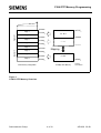
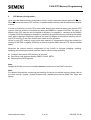
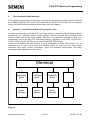
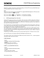
Microcontrollers
ApNote
AP1639
: Additional file
AP1639xx.EXE available
In-System Programming of C164-8E OTP Devices
Siemens C164CI-8E 16-bit microcontrollers provide 64 KByte OTP memory on-chip.
This application note gives hints and examples for in-system programming of C164CI OTP
devices. Memory programming and memory uploading is supported by the Windows-based
memory tools “Memtool” and “ROM_UP”.
Author : Peter Kliegelhöfer / HL MD AE Microcontroller Application Support
Semiconductor Group
02.99, Rel 02
C164 OTP Memory Programming
Contents
Page
1
OTP Memory Overview . . . . . . . . . . . . . . . . . . . . . . . . . . . . . . . . . . . . . . . . . . . . . . . . . . 3
2
OTP Memory Configuration . . . . . . . . . . . . . . . . . . . . . . . . . . . . . . . . . . . . . . . . . . . . . . 5
3
CPU Host Mode (CHM) Selection. . . . . . . . . . . . . . . . . . . . . . . . . . . . . . . . . . . . . . . . . . 6
4
4.1
Memtool - The on-chip OTP/ Flash Memory Programming Tool . . . . . . . . . . . . . . . . 6
Special Memtool Options . . . . . . . . . . . . . . . . . . . . . . . . . . . . . . . . . . . . . . . . . . . . . . . . 7
5
Pits, Traps and Mines . . . . . . . . . . . . . . . . . . . . . . . . . . . . . . . . . . . . . . . . . . . . . . . . . . . 7
6
6.1
OTP Programming Drivers Overview . . . . . . . . . . . . . . . . . . . . . . . . . . . . . . . . . . . . . . 8
Program Verify . . . . . . . . . . . . . . . . . . . . . . . . . . . . . . . . . . . . . . . . . . . . . . . . . . . . . . . . 9
7
ROM_UP - The on-chip OTP/ Flash/ ROM Memory Upload Tool. . . . . . . . . . . . . . . . 10
AP1639 ApNote - Revision History
Actual Revision : 02.99
Previous Revision : 03/98
Page of
Page of
actual Rev. prev.Rel.
7
7
chapter 5 updated
8
8
chapter 6 updated
MEMTOOL.EXE and programming drivers updated
Semiconductor Group
2 of 10
AP1639 02.99
C164 OTP Memory Programming
1
OTP Memory Overview
The C164CI devices provide 64 KBytes of one-time-programmable „OTP“ memory on-chip for both
instruction code and constant data.
The C164CI OTP module is a 512 KBit memory organized as 16K double words of 32 bit each.
On its CPU interface it presents a fast read access (60ns @ fCPU = 25 MHz) of 32 bit in one machine
cycle. Read accesses of code and data are possible in any addressing mode, thus realizing the
highest CPU performance with fetch and execution of double word instructions in a single
instruction cycle.
For programming and testing purposes a special interface is realised which directly connects the
OTP module to an external or internal (CPU) host. Programming is performed in steps of 16-bit
words, needing typically 100 µs per word. Special algorithms for over-/ under-programming, with
verify operations, are not necessary. The programming voltage is supplied on the EA/ VPP pin.
Unprogrammed OTP memory cells contain all ’1’s.
The OTP memory can be programmed both in an appropiate programming board (supplier: Ertec,
SMS, Data I/O) or in the target system which provides a lot of flexibility.
The lower 32 KBytes of the on-chip OTP memory of the C164CI can be mapped to either segment
0 (00’0000H to 00’7FFFH) or segment 1 (01’0000H to 01’7FFFH) during the initialization phase to
allow external memory to be used for additional system flexibility. The upper 32 KBytes of the onchip OTP memory are assigned to locations 01’8000H to 02’0000H (figure 1).
Semiconductor Group
3 of 10
AP1639 02.99
C164 OTP Memory Programming
02’0000H
Segment 1
Page 7
Page 6
Page 5
Page 4
Segment 0
Page 3
Page 2
Page 1
Page 0
Sector 1
32 - 64 K
(32K)
01’C000H
00’8000H
01’8000H
01’4000H
0 - 32 K
01’0000H
00’C000H
00’FFFFH
00’0000H
Mapping
00’8000H
00’4000H
0 - 32 K
00’0000H
00’0000H
C16x Memory Configuration
64 KByte OTP Memory
Physical
OTP Address
Figure 1
C164CI OTP Memory Overview
Semiconductor Group
4 of 10
AP1639 02.99
C164 OTP Memory Programming
2
OTP Memory Configuration
Upon reset the default memory configuration of the C164CI is determined by the state of its EA pin.
When EA is low the internal OTP memory is disabled and the startup code is fetched from external
memory.
In order to access the on-chip OTP memory after booting from external memory the internal OTP
memory must be enabled via software by setting bit ROMEN in register SYSCON. The lower 32
KBytes of the OTP memory can be mapped to segment 0 or segment 1, controlled by bit ROMS1
in register SYSCON. Mapping to segment 1 preserves the external memory containing the startup
code, while mapping to segment 0 replaces the lower 32 KBytes of the external memory with onchip OTP memory. In this case a valid vector table must be provided.
As the on-chip OTP memory covers more than segment 0, segmentation should be enabled (by
clearing bit SGTDIS in register SYSCON) in order to map the whole internal OTP into the address
space.
Whenever the internal memory configuration of the C164CI is changed (mapping, enabling,
disabling) the following procedure must be used to ensure correct operation:
l
l
l
Configure the internal OTP memory as required
Execute an inter-segment branch (JMPS, CALLS, RETS)
Reload all four DPP registers
Note:
Register SYSCON can only be modified before the execution of the EINIT instruction.
Note:
For detailed informations concerning the handling of internal non-volatile memory please refer to
the users manual, chapter „System Programming“ (Handling the Internal ROM/ Pits, Traps and
Mines).
Semiconductor Group
5 of 10
AP1639 02.99
C164 OTP Memory Programming
3
CPU Host Mode (CHM) Selection
For in-system programming it is necessary to activate the programming interface which is realized
as an XBUS peripheral. The C164CI enters CHM with port pin P0L.2 low during reset. It is useful to
combine this mode with the bootstrap loader mode (see next chapter).
4
Memtool - The OTP/ Flash Memory Programming Tool
In-system programming of on-chip OTP- and Flash memory is supported by the Windows-based
programming tool „Memtool“ which is freely available. Siemens provides driver updates on the
Internet; please ask for the current status. Memtool is an application example as well as a
programming tool for on-chip OTP- and Flash memory, supporting C161CI-32F, C167CR-16F,
C167CS-32F and C163-16F Flash devices and C164CI-8E OTP devices.
Thanks to the modular structure Memtool is easily expandable for future C16x devices. For an
interested user all driver sources are also available (figure 2). Along with the drivers come
readme.txt files which contain informations about the hardware requirements and latest
informations about Memtool and each driver.
Memtool
C163 Flash
Driver
C167 Flash
Driver
C164 OTP
Driver
Driver
Sources
Driver
Sources
Driver
Sources
Figure 2
Semiconductor Group
6 of 10
AP1639 02.99
C164 OTP Memory Programming
All software including the programming data is downloaded from a host PC into the internal RAM of
the microcontroller. The application expects only internal RAM, external RAM is not required.
For OTP programming an additional programming voltage (e.g. 11,5 V) has to be applied to pin EA/
Vpp. Please check for the right Vpp value in the data sheet.
In order to download the application from a PC, a serial link has to be established. The C164CI
already provides an asynchronous serial interface that only has to be connected to COM1 or COM2
of your PC. Supposing you are using a Phytec C164CI starter kit, you can directly connect its serial
connector with the COM1/ COM2 interface of your PC.
Note:
For getting started two steps are needed:
1.) Activate bootstrap loader mode and enter CPU host mode (these modes are activated with port
pins P0L.2 and P0L.4 “LOW” during reset; simple 8.2k pull down resistors are applicable)
2.) Connect the target with the C164CI device to a host PC with a serial cable.
4.1
Special Memtool Options
For default Memtool expects serial communication via RS232. Some drivers also support singlewire transmission (K-Line). All drivers which support K-Line protocol are marked with “KL” (see box
“Target”/ “Change”/ “Select Controller Type”). Select the desired mode (RS232 or K-Line) in box
“Interface” / “Setup Interface”.
In some cases it is also useful to get a LOG-file of the transmitted data. For LOG-file generation
switch “DIAGLOG” in the Memtool configuration file (memtool.ini/ siemtool.ini) has to be set to “1”.
The LOG-file will be closed by leaving Memtool. A set box for the LOG switch is currently not
implemented.
5
Pits, Traps and Mines
To prevent the controller from beeing damaged, generally main power must be connected before
and disconnected after Vpp. Also the microcontroller has to be in a programming mode (CHM or
EHM) when applying Vpp. In case of in-system programming via Memtool the controller must be in
CHM programming mode.
The data transmission speed via K-line (single-wire) can be increased, when the FIFO of the used
communication port (COM1, COM2) of the PC is deactivated.
The C164CI enters bootstrap mode if pin P0L.4 is sampled low at the end of a hardware reset. In
this case the BSL is activated, independent of the selected bus mode; no evaluation of pin EA
(external access) in bootstrap loader mode.
In CPU host mode (CHM) the default setting of bit BUSACT0 in register BUSCON0 is “1”, which
means: external bus enabled. In single-chip applications this might could lead to problems with
external peripherals, because accesses to the OTP programming interface (respectively to the
registers OPAD, OPDAT, OPCTRL) can be seen externally. In this case it is necessary to reset bit
BUSACT0 before performing the first OTP programming interface access. The default setting of
Semiconductor Group
7 of 10
AP1639 02.99
C164 OTP Memory Programming
BUSACT0 in CHM is independent of SYSCON settings. All C164 OTP drivers set BUSCON0 (and
therefore BUSACT0) to zero in module “load_2”.
Note:
Since device step CA the setting of bit BUSACT0 in register BUSCON0 depends in CPU host mode
(CHM) on the state of pin EA during reset:
P0L.2 “low” (CHM) and EA “low”: BUSACT0 = “1” (external bus enabled)
P0L.2 “low” (CHM) and EA “high”: BUSACT0 = “0” (external bus disabled)
6
OTP Programming Drivers Overview
Several OTP programming drivers are available. This is founded on different demands of different
applications. The following overview is just a snapshot of the status quo. In the future new versions
will be available which will partly replace the current ones. Please pay attention to the readme.txt
files which come along with the drivers.
Due to the fact that up to design step BC it not possible to perform OTP read accesses in CPU host
mode (CHM), the success of an OTP programming operation can only be verified in normal mode
by reading the OTP content via ROMbus (see chapter 6.1).
Since design step CA read accesses to the OTP can be also performed in CHM. Read accesses
(like write accesses) are controlled via the operation control register OPCTRL. Normal data read
accesses without the right OPCTRL setting would deliver dummy zero values “0000 H” as long as
the controller is in CHM.
Furthermore it is necessary that during verify read accesses Vpp level is limited to 5 Volt or lower.
All C164 OTP drivers are properly tested with 9600 Baud transmission rate.
The readme.txt files in the sub-directories of Memtool (memtool/ siemdrv/ C16x...) contain important
informations about each driver version:
C164CI Standard
- RS232
- external bus disabled (BUSCON0=0000h)
- no EINIT
- system clock output not enabled
- no Vpp switching control via port pin
C164CI cv_A (customized version A)
- RS232
- external bus disabled (BUSCON0=0000h)
- no EINIT
- system clock output enabled
- no Vpp switching control via port pin
Semiconductor Group
8 of 10
AP1639 02.99
C164 OTP Memory Programming
C164CI Phytec Starterkit
- RS232
- external bus disabled (BUSCON0=0000h)
- EINIT instruction in modules “progp” and “vefy”
- system clock output not enabled
- Vpp switching control via port pin P8.3
C164CI KL cv_B (customized version B)
- K-Line
- external bus disabled (BUSCON0=0000h)
- EINIT instruction in modules “progp” and “vefy”
- system clock output not enabled
- Vpp switching control via port pin P1L.0
C164CI cv_C (customized version C)
- RS232
- external bus disabled (BUSCON0=0000h)
- no EINIT
- system clock output enabled
- no Vpp switching control via port pin
6.1
Program Verify
With current Memtool drivers a verification of OTP programming can only be performed when the
CPU is in normal mode. Be aware that the CPU is still in CPU host mode (CHM) after programming.
All verify attempts will fail as long as the CPU is not in normal mode, regardless of the content of the
OTP memory.
For entering normal mode it is necessary first to disconnect the pull-down resistor at port pin P0L.2
and then to reset the controller (pin P0L.4 has to remain unchanged “low” for bootstrap loader
mode). In module “vefy” which performs a comparison of the content of the OTP memory and the
source data bits ROMEN and ROMS1 of register SYSCON will be set to “1” in order to enable
internal OTP memory and to map the lower 32k OTP memory to segment 1 (see user’s manual:
“Memory Organization”).
7
ROM_UP - The on-chip OTP/ Flash/ ROM Memory Upload Tool
Attached there is an Windows-based utility “ROM_UP20” which allows to upload the content of
OTP-, Flash- and ROM memory (blocks of 32k...256k are currently supported) by using the
bootstrap loader. The uploaded data can then be stored into a file (helpful and necessary for a filecompare).
Semiconductor Group
9 of 10
AP1639 02.99
C164 OTP Memory Programming
Following a short description of ROMUPV2.EXE:
Self extracting utility program to upload contents of internal Flash/ ROM memory via bootstrap
loader.
In combination with a bootstrap loader which is executed from the internal flash, this program allows
to upload the content of internal Flash/ OTP/ ROM memory via the serial port and optionally to write
the uploaded data into a file.
When ROM Upload V2.0 is invoked,
- click on box in the second line on the left side near loader program
click on field “load...”
- select file “loader.hex”
(since the example bootstrap loader only accepts 32 bytes (like the integrated bootstrap loader), a
second loader (loader.hex) must be used to load larger programs)
- click on field “load...” on the right side of third line
- select desired upload program according to desired/ maximum memory size of your controller
(64kb.h67 will read entire memory of C164CI-8E, 32kb.h67 will read first 32 Kbyte of memory)
Note: first 32Kbyte (0000h...7FFFh) of memory is always mapped to segment 1 (1’0000h...1’7FFFh)
by file “loader.hex” in order to have linear addresses.
Semiconductor Group
10 of 10
AP1639 02.99