1
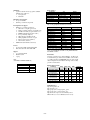
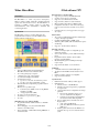
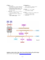
DE NAYER Instituut
J. De Nayerlaan 5
B-2860 Sint-Katelijne-Waver
Tel. (015) 31 69 44
Fax. (015) 31 74 53
e-mail: [email protected]
[email protected]
[email protected]
website: emsys.denayer.wenk.be
- OVERVIEW EXCALIBUR
LEON
MICROBLAZE
NIOS
OPENRISC
VIRTEX II PRO
Version 1.1
HOBU-Fonds
Project IWT 020079
Titel
:
Projectleider:
Auteur
Embedded Systeemontwerp op basis van
Soft- en Hardcore FPGA’s
Ing. Patrick Pelgrims
:
Ing. Dries Driessens
Ing. Tom Tierens
Copyright (c) 2003 by Patrick Pelgrims, Tom Tierens and Dries Driessens. This material may be
distributed only subject to the terms and conditions set forth in the Open Publication License, v1.0 or
later (the latest version is presently available at http://www.opencontent.org/openpub/).
- 1/13 -
Altera EXCALIBUR
32-bit hardcore CPU
Introduction
MMU
standard ARMv4 MMU mapping sizes, domains and
•
access protection scheme
provides translation and access permission checks
•
for instruction and data addresses
•
fully configurable memory map
•
mapping sizes are 1MB(sections), 64KB(large
pages), 4KB(small pages) and 1KB (tiny pages)
16 domains implemented in hardware
•
•
64 entry instruction Transfer Look-aside Buffer
(TLB) and 64 entry data TLB
•
hardware page table walks
round-robin replacement algorithm (cyclic)
•
Excalibur™ devices integrate a 200-MHz 32-bit
ARM922TTM
processor, on-chip SRAM, SDRAM
controller and several other peripherals with the
APEX™ 20KE FPGA architecture, balancing the price,
performance, and system integration requirements of
system-on-a-programmable-chip (SOPC) designs. The
microprocessor subsystem is implemented as an
“embedded stripe” next to the “FPGA stripe”.
Specifications
Memory support
•
internal single-port SRAM up to 256 KB
internal dual-port SRAM up to 128 KB
•
•
internal SDRAM controller
supports single data-rate (SDR) and double
data-rate (DDR)
up to 512 MB
Data rates to 133 (266) MHz
Expansion Bus Interface (EBI)
•
Compatible with industry standard flash
memory, SRAM and peripheral devices
Four devices, each up to 32 MB
Bus architecture
uses 2 AMBA V2.0 processor busses
•
(AHB1 and AHB2)
each bus has 32-bit address, read and write buses
•
•
ARM-designed high-performance bus standard that
is optimized for high-speed cache interfaces.
•
AHB1 runs at the processor speed
(up to 200 MHz, single master bus)
•
AHB2 serves as the peripheral bus (runs at one-half
of the AHB frequency, multi-master bus)
Processor
•
ARM9TDMI processor core with 32-bit Harvard
architecture
•
ARM v4T instruction set (32 bit load and store
instruction set)
•
Instruction set supports 16 and 8 bit memories
5 stage pipeline
•
•
supports little & big endian modes
task identifier register for real time operating system
•
(RTOS) support
PLD (re)configuration possible via the embedded
•
processor software
32x8bit hardware multiplier
•
•
no hardware divider
no FPU
•
Timer
•
general-purpose dual-channel timer
32-bit timer register
32-bit clock pre-scaler
3 operating modes:
free running interrupt
interval timer
one-shot interrupt
watchdog timer
•
Cache
8 KB instruction cache
•
•
8 KB data cache
8 word line length, one valid bit, two dirty bits,
•
allowing half word write-backs
selectable pseudo-random or round-robin
•
replacement
independently-lockable caches with granularity of
•
1/64th of cache
four-word write buffer, with 4 addresses
•
•
virtually addressed 64-way set associative cache
write-trough and write-back cache operation
•
supported
Interrupt controller
provides a simple, flexible interrupt system
•
•
up to 17 interrupt sources:
10 interrupts from modules within the
embedded stripe
1 external interrupt source
6 interrupts from the PLD-stripe (can be treated
as a bus)
Extended programmable on-chip peripherals
embedded stripe PLLS
•
universal asynchronous receiver/transmitter (UART)
•
•
general purpose I/O port
- 2/13 -
•
ETM9 embedded trace module to assist software
debugging
Debugging
•
SignalTapTM embedded logic analyze
ARM® JTAG processor debug support
•
•
real time data/instruction processor trace
•
background debug monitoring via JTAG interface
SOPC builder - synthesis
•
intuitive GUI simplifying system definition and
customization
•
wizard interface for customization of each
component
automatically-generated logic integrates processor,
•
memories, peripherals, IP-cores, on-chip buses and
bus arbiters
•
creates VHDL/Verilog HDL code for system
connection
software development environment generated to
•
match the target hardware
Simulation
support for:
Quartus II simulator
•
•
Cadence NC-Verilog and NC-VHDL simulators
ModelSim simulator
•
•
Synopsys VCS simulator
Software
•
Quartus II development environment includes:
Integrated hardware and software development
environment
C/C++ compiler, source level debugger, RTOS
support
Operating Systems
Accelerated Technology: Nucleus PLUS RTOS
•
•
Micriµm: µC/OS-II, the Real-Time Kernel
Microtronix: Linux
•
•
MiSPO: NORTi RTOS
•
MontaVista Software: Linux
OSE Systems: OSE RTOS
•
•
Shugyo Design Technologies: KROS
Performance
•
performance ratio of 1.05 MIPS per MHz
processor running @ 200 MHz
•
References
•
www.altera.com/products/devices/arm/
Excalibur Devices Hardware Reference Manual
•
•
ARM922T Technical Reference Manual
ARM9TDMI Technical Reference Manual
•
- 3/13 -
LEON - 2 1.0.10
32-bit softcore CPU
Introduction
The LEON VHDL model implements a fully synthesisable 32bit processor with an instruction set according to the IEEE1754 (SPARC V8) standard. The processor was initially
developed by Jiri Gaisler while working for the European
Space agency (ESA). Gaisler Research is now maintaining and
further enhancing the model under ESA contract. The LEON
is designed for embedded applications, the implementation is
focused on portability and low complexity.
Specifications
Debug support unit (DSU)
•
Optional, no impact on performance
Non intrusive debugging on target hardware us
•
•
Seamless connection to gdb, allowing on-chip
debugging
•
Allows insertion of data and instruction watchpoints and
access to all on-chip registers from a remote debugger
Trace buffer to trace executed instruction flow and/or
•
AHB-bus traffic
Communication to DSU using a dedicated UART
•
Memory controller
Direct interface to :
•
PROM
SRAM
memory mapped I/O devices
SDRAM (supports up to two banks of
PC100/PC133 compatible devices)
2 Gbyte address space
•
•
memory areas can be programmed to 8 – 16 –32 bit data
width (SDRAM supports only 32 bit)
The LEON SPARC consists of several modular units.
Power management
Power-down mode supported, effective halt of integer
•
unit, wake-up on interrupt
Integer unit (IU)
32-bit RISC architecture implementing the IEEE-1754
•
standard (SPARC V8) instruction set including all
multiply and divide instructions
5 stage instruction pipeline
•
•
8 global registers
•
2-32 register windows of 16 registers each
configurable multiplier
•
•
32-bit instructions
16x16 bit MAC with 40-bit accumulator
•
•
non restoring Radix-2 divider
Custom and optional units
•
direct interface to the MEIKO FPU, which is part of
SUN’s Micro Sparc, available under the Sun’s
Community licensing (SCSL)
An open-source IEEE-754 FPU exists, but is still
•
incomplete
•
general interface to connect to other floating-point
units/custom units allowing parallel or sequential
execution with the IU
Timer unit
•
The timer unit implements:
two 24-bit timers.
one 24-bit watchdog timer.
•
Shared 10-bit prescaler value
Interrupt controller
15 maskable interrupt sources
•
•
two interrupt priorities
optional chained interrupt controller providing 32
•
additional interrupts.
System interface
•
Full implementation of AMBA AHB and APB buses
(V2.0)
•
All provided peripherals use the AMBA AHB/APB
interface making it easy to implement more of them or
using them as an example.
Parallel I/O port
32 bit I/O port:
•
16 bit shared with memory bus
16 bit individually programmable
Cache
•
Harvard model with split instruction and data
Instruction/data cache size scalable from 1KB to 64KB
•
•
Direct mapped or multi-set cache with set associativity of
2-4
•
Cache lines with 8-32 bytes of data
Supporting 3 replacement policies: least recently used,
•
least recently replaced and pseudo-random.
Data cache can perform bus-snooping on AHB-bus
•
- 4/13 -
Synthesis
•
the VHDL model is fully synthesisable
•
synthesis scripts available for:
Exemplar Leonardo
Synopsys FPGA-compiler
Synopsys-DC
Synplify
Simulation
•
a generic testbench and test program is available,
including support files for:
Synopsys VSS
Modelsim
Facts & figures
Technology
%
'( () * ' $+
$ $
'
$
$
%
0
,& - . ! /
, 1, ,
1 2
0
!
!
!
%3
%
0
!" #
!" #
!" #
!" #
!" #
!" #
!" #
(The area in the table reflects the complete LEON-1 2.3.3
with on-chip peripherals and memory controller)
Development tools support
LECCS cross compiler system (free)
•
GNU C/C++ compiler (gcc-2.95.2)
Linker, assembler, archiver etc. (binutils-2.11)
Standalone C-library (Cygnus newlib-1.8.2)
RTEMS real-time kernel (rtems-4.5.0+)
Boot-prom utility (mkprom)
GNU debugger with Tk front-end
DDD graphical user interace for gdb
Remote target monitor (rdbmon)
DSU monitor (dsumon)
TSIM architectural simulator (licensed)
•
Technology
4
4
4
4
'( () *
'( () *
'( () *
'( () *
'( () *
'( () *
License
Leon model available unnder GNU LGPL
•
•
Files and testbenches under GNU GPL
+
+
+
+
(
(
(
(
Area
1'$
1 '
1'$
1 $'
1' 55 $ 0
1' 55 $ 3
!) $
!) $ 3
(* $
(* $ 0
*
%
*
* $4
0
* $4
00
) $1
) $1
0
,1
3,1
$ 3,1
$ %,1
% 3,1
% 3,1
0 ,1
0 ,1
% 00 , 5
%
,5
%
,5
% 3$ , 5
% $% , 5
% $% , 5
Timing
$
%
%$
%3
3
$%
3
3
1
1
1
1
1
1
%
The area in the table reflects the complete leon-2 1.0.10
(cache, internal PROM) with 8KB on-chip AHB RAM, DSU
and SRAM controller.
Support
•
good, updated manual
Gaisler research
•
e-group
•
Performance
Using 4k + 4k caches and a 16x16 multiplier, the Dhrystone
2.1 benchmark reports 1550 iterations/s/MHz, this translates
to roughly 0.85 dhrystone MIPS/MHz using the VAX 11/780
value. Configurations with mul/div and larger caches usually
perform somewhat better.
Area
(used FPGA: APEX20K1000E-1X )
module
Leon (+cache +DSU)
HW mul/Div (5cycle)
SDRAM ctrlr
MEIKO FPU
Timing
$
$
&
Operating system support
•
eCos port available
uCLinux port under developement
•
Area
size
8186 LE
1635 LE
594 LE
6151 LE
Implementation results
'( () * + ( * 1
1
4 1'$ / $ $'
.(
! ."
4 1'$ / $ $'
.(
! ."
4 1'$ / $ $'
$.(
! ."
4 1'$ /
1 $'
'( () * + ( * 55
$
$
$
0
$
$
$
$
$
$
%
%
$
0
$
$
0$ 0
$
% 300
%
$0
$
%
6
*using the dhrystone 2.1 benchmark
Links/References
http://www.gaisler.com
http://www.leox.org
http://groups.yahoo.com/group/leon_sparc/
http://groups.yahoo.com/group/leon_dev/
http://www.sun.com/processors/communitysource/
LEON-2 Processor User’s Manual (Version 1.0.10)
- 5/13 -
Xilinx MicroBlaze
32-bit softcore CPU
Introduction
The MicroBlaze is a 32-bit soft processor developed by
Xilinx. It features a RISC architecture with Harvard-model
separate data and instruction busses. The MicroBlazeTM is
designed for building complex systems for networking,
telecommunication, data communication, embedded and
consumer applications.
Specifications
The MicroBlaze consists of several modular units. All
peripherals mentioned below come with a OPB V2.0 bus
interface with byte-enable support.
External memory controller (EMC)
Supports up to 8 memory (flash/SRAM) banks
•
•
Separate control register for each bank
•
Supports 8,16,32 and 64-bits bus interface
Supports memory width of 8,16,32 and 64-bits.
•
•
Memory width is independent of OPB bus width
Configurable wait states for read, write, read in page,
•
read recovery before write, and write recovery before
read
Optional faster access for in-page read accesses (page
•
size 8 bytes)
Timer/counter
•
Two 32-bit programmable interval timers with interrupt,
compare, and capture capabilities
•
One Pulse Width Modulation (PWM) output
Watch Dog Timer (WDT) with selectable timeout period
•
and interrupt
Supports 8, 16 and 32-bit bus interfaces
•
Interrupt controller
Number of interrupts inputs is configurable up to the
•
width of the data bus
can be easily cascaded to provide additional interrupt
•
inputs
Programmer interface similar to Virtex™ II Pro
•
interrupt controller IP (IntC)
•
Master Enable Register for disabling the interrupt
request output
•
Supports data bus widths of 8, 16 and 32-bits
Processor
•
True 32-bit RISC architecture implementing the
MicroBlaze instruction set architecture (ISA)
•
32 x 32-bit general purpose registers
1 instruction per cycle, 3-stage pipeline
•
•
Uses hardware multiplier (if available)
32-bit instruction words
•
type A: two source and one destination operand
type B: 1 source and one immediate operand
Harvard architecture, implementing separate instruction
•
and data bus.
Memory access possible trough:
•
local memory bus (LMB) (for fast on-chip BRAM,
maximum 2 x 256kB)
on-chip peripheral bus (OPB)
•
No support for custom instructions
No interface for co-processors (e.g. FPU)
•
•
No cache
Xilinx Microprocessor debugger (XMD)
•
Program that facilitates a unified interface to the GDB +
Tcl debuggers
•
Allows debugging on a cycle-accurate MicroBlaze
instruction set simulator (ISS)
•
Allows debugging of a MicroBlaze running XMDstub on
a hardware board
- 6/13 -
UART Lite
•
1 Transmit and 1 Receive channel (full duplex)
16-character transmit FIFO and 16-character receive
•
FIFO
Number of databits, baud rate is configurable
•
•
Supports 8-bit bus interfaces
System interface
OPB V2.0 bus interface with byte-enable support.
•
•
OPB Arbitration
arbitrates between 1-16 OPB Masters
arbitration priorities among masters programmable
via register write
priority arbitration mode configurable via a design
parameter :
Fixed priority arbitration with processor
access to read/write Priority Registers
Dynamic priority arbitration implementing a
true least recent used (LRU) algorithm
Two bus parking modes selectable via Control
Register write:
park on selected OPB master
park on last OPB master which was granted
OPB access
Watchdog timer which asserts the OPB time-out
signal if a slave response is not detected with 16
cycles
GPIO
•
Each GPIO bit dynamically programmable as input or
output
•
Number of GPIO bits configurable up to size of data bus
interface
Can be configured as inputs-only to reduce resource
•
utilisation
Supports 8, 16 and 32-bit bus interfaces
•
Synthesis
Xilinx Platform Studio (XPS)
•
•
Netlist in 2 ways: Flat or Hierarchical
•
Hierarchical - 2 Implementation Tool Flows:
XPS (4 synthesis tools available: XST, Leonardo, FPGA
•
Compiler II and Synplify)
•
Xilinx ISE (Best area and speed results: more than 300%
faster- and more than 30% smaller designs)
•
Flat (only XPS)
Simulation
•
XMD includes SimGen (Simulation Generator)
•
Generates automatically simulation models for
MicroBlaze and IPs
Generates ModelSim DO file
•
•
Behavioral, Structural or Timing simulation models
Platform Tailoring Utilities
Platform Generator:
•
tailors each bus component
generates a custom
Library Generator:
•
customised device drivers
software function libraries for the given user defined
hardware processor system generated by Platform
Generator
Development tools support
•
Xilinx software integrated development environment,
which creates software (like device drivers, standard C
libraries,…) that matches the selected hardware.
•
GNU C-compiler tools including compiler, assembler,
debugger, …
Facts & figures
The following synthesis results were obtained with Xilinx ISE
and its integrated XST synthesis. The Microblaze system is a
simple system with 4kB on-chip RAM, a jtag uart and some
GPIO pins.
Technology
+
+
+
+
+
+
(
(
(
(
(
(
*
*
*
*
*
*
7
70
7%
7
$
7%
$
7
$4 ! 07
$ 4 ! 0 70
Area
% (
% (
(
(
$0
$0
$ (
$ (
module
54 58 6
9
: ))
54 58 6
9$ : ))
42 1
8 :9
42 1
8 :9
42 1
8 :9
42 2
!) !
42 66
!) !
42 6
!) !
42 =
1: )
42 =
1: )
42 =
1: )
4 2 ! 4 58" 2 (
42 - & ! ( , <
42 - & ! ( , <
4 2 ()
: ))
4 2 5$
@
>#
4 2 4 5 @ 9? = *
54 58 5) "
!) ! 9
4 2 5) "
!) !
42 &
- ,( ! C42 -( .
=D 6 4 2 -( = !")
4 2 A 4 5 9 5=
4 2 A 4 5 9 5=
4 2 A 4 5 9 5=
4 2 A 4 5 9 $ 5=
Performance
9 ) ; 2 - #9
9 ) ; 2 - #9 $
9 ) ; 2 - #9
Logic Cells
%
0
$
$%
$
6 <(
6 <(
6 <(
0
$
0
> #9 ? =6
@ A
, ( > #9 8 " 6 " *
, ( > #9 B 6 " *
$= # > #9 ? =6
@ A
$ < > #9 ? =6
@
$
> #9 ? =6
@
6 , > #9 ? =6
@ A
@ - * 8 58
5) "
9 $ 5) "
A
Device Family Speed
+ ( * 55 4 ! #
+ ( * 55 #
$
+ ( * 1 0#
0
) 551 0#
0
) 55 #
'(
#
'(
0
$3
$
$
$ %
%%
#
3$
$
$
$
%
Performance Logic Cells
$ 6 54
3
$ 6 54
3
%3 6 54
%3 6 54
% 6 54
(without off-chip memory)
Operating system support
•
µC/OS-II RTOS port under development.
) $1
) $1
Area
Following estimated Logic Cells were calculated with the
Field Programmable Controller Calculator. This is an online
tool that calculates MicroBlaze IP core size usage in SpartanIIE devices.
Timing
0$
%
%
$%
%
- 7/13 -
Links/References
http://www.xilinx.com
http://ucos-ii.com/contents/products/ucos-ii/ports.html
Altera NIOS
32-bit softcore CPU
Introduction
The Nios embedded processor is a soft core CPU, introduced
in 2000, optimized for Altera programmable logic devices and
system-on-a-programmable chip (SOPC) integration. It is a
configurable, 16- or 32-bit general-purpose RISC processor
with a single issued, 5-stage pipelined Harvard architecture
and a compiler-friendly instruction set. The principal features
of this instruction set architecture are: a large, windowed
register file; 16bit instructions for both versions; powerful
addressing modes and easy extensibility. The Nios can easily
be configured using the Altera’s SOPC-Builder which
automatically generates arbiters for all include peripherals and
user logic. The SOPC-Builder includes also several
peripherals, including a UART, timer, PIO, SPI, (S)SRAM,
SDRAM, Flash, DMA, PWM and IDE. All these peripherals
connect to the Avalon bus of the Nios. The Nios kit also
comes shipped together with Redhat’s GNUPro toolkit.
It includes a compiler, an assembler, a debugger and several
utilities. Additional development kits support µClinux,
Ethernet and on-chip debugging with tracing.
Specifications
Multiplier
•
3 types of multipliers:
software implementation
MSTEP hardware implementation
full 16x16bit hardware
•
Floating point unit:
software implementation;
full implementation in the future.
Custom Instructions
Custom instruction logic extends Nios instruction set
•
•
Accelerates software algorithms: reduces number of
operations for “inner loop” tasks to a single cycle
•
Single-cycle (combinatorial) or multi-cycle (sequential).
Interrupt Service Routine Handler
•
Up to 64 prioritized, vectored interrupts
16 interrupt are reserved for system services
•
•
48 interrupt vectors for user applications
Memory
•
8, 16 or 32-bit on- and off-chip memory
•
On-chip memory: embedded system blocks (ESBs)
Off-chip memory: active serial memory interface,
•
SDRAM-, SSRAM-, flash- and SRAM-controllers
•
Any user-defined interface may be created to connect
other off-chip memory devices
Nios Processing Unit
Pipelined RISC architecture
•
•
Single issue, 5-stage pipeline
•
Harvard architecture
Instruction set contains:
•
arithmetic and logical operations
bit operations
byte extraction
data movement
control flow modification
conditionally executed instructions
Registers:
•
128, 256, or 512 registers
Register width: width of CPU data path
32-register sliding window with 16-register
granularity
Register file behaves like a stack
CWP (Current Window Pointer) Manager routine
handles details of manipulating register file during
subroutine calls
Several machine-control registers
Program counter
K register used for instruction prefixing.
- 8/13 -
Avalon Bus
Simultaneous access to memory resources for the Nios
•
embedded CPU together with high-bandwidth
peripherals
•
Nios: only traffic-management tasks
Slave-side arbritation
•
Simulation
Simulation with Modelsim
•
•
SOPC Builder creates project-files for Modelsim
GERMS
•
Mnemonic for minimal command set of monitor
program:
Go (run a program)
Erase flash
Relocate next download
Memory set and dump,
Send S-records.
•
Also contains software routines for writing to and
erasing Advanced Micro Devices (AMD) flash devices
•
Connection via UART
GNU Debugger (GDB)
•
Requires special hardware components
Starts programs and specifies anything that might affect
•
its behavior
Stops programs based on a set of specific conditions
•
•
Examines what happened once programs stop
Changes programs to fix bugs and continue testing
•
•
Supports programs written in assembly, C, or C++.
O.S.
•
Especially commercial operating systems
Nucleus Plus, real-time OS from Accelerated Tech.;
•
NORTi CE, µITRON compliant real-time OS;
•
•
The µClinux kit from Microtronix.
µC/OS-II, a real-time, multitasking kernel from Micrium
•
•
KROS, a POSIX-compliant OS from Shuygo Design
Expandability
•
SOPC Builder has “interface to user logic” wizard
•
Free AMBA bridges
‘SOPC Builder ready’ cores can be evaluated
•
Component
Nios 32-bit
Nios 16-bit
+ Debug
UART
PIO
TIMER
Type
Minimum
Standard
Maximum
Minimum
Standard
Maximum
HW breakpoint
ext. Trace buffer
No Par., 8bit
input
output
input+output
bidir. Tri-state
full
simple
watchdog
LE
1290
1500
2025
950
1140
1270
+530
+300
170
2/bit
1/bit
3/bit
3/bit
232
100
103
Facts & Figures
1) Synthesis Comparison
•
Full featured Nios
1kB GERMS-monitor
•
On-chip ROM
•
•
16kB on-chip RAM
2 simple UARTS
•
•
2 simple timers
2 SDRAM controllers for in total 128MB
•
•
Some GPIO pins
•
APEX20KE1000-2X FPGA
Synthesis tool
Speed Area
Power consumption
SOPC Builder + Quartus
Leonardo Spectrum
Synplify
40MHz
40MHz
40MHz
4663 LE 551mA @ 5V
4580 LE 420mA @ 5V
4123 LE 450mA @ 5V
Remark the difference in power (100mA)
Low-level-architecture-specific stuff had to be left out
Is probably the cause of this huge difference
2) Target Comparison
Full featured Nios
•
•
Simple UART,
1kB GERMS-monitor on-chip ROM
•
•
8kB on-chip RAM
ESB
5
9
16
3
5
8
0
0
0
0
0
0
0
0
0
0
Target
Apex20KE
1000
Grade
-2X
-1X
Apex II 25
-7
-9
Cyclone 12 -6
-8
Stratix 10
-5
-7
LE= Logic Element
ESB= Embedded System Block (~ramblock)
SOPC Builder
“From concept to system in minutes”
•
•
Automatic bus connections, interrupt numbering and
memory ranges
Changes to any memory, interrupt number or clock
•
frequency automatically reconfigures all other necessary
settings.
Synthesis
In Quartus as a ‘block’
•
•
VHDL Nios system with any synthesis tool
Tool
Quartus
Synplify
Synplify
Size
3804LE
3634LE
3632LE
Speed
58MHz
55MHz
60MHz
Quartus
Synplify
Synplify
Synplify
Synplify
Synplify
Synplify
2420LE
2389LE
2400LE
3472LE
3697LE
3339LE
3115LE
100 MHz
98MHz
71MHz
120MHz
94MHz
123MHz
97MHz
Time
9m14s
94s+7m19s
104s+7m11
s
5m31s
74s+5m36s
90s+4m50s
72s+4m42s
65s+5m00s
72s+4m12s
65s+4m12s
License
•
Free evaluation version for Quartus subscribers
OpenCore Plus license: one-hour time limit
•
•
Full Nios in Nios development kit
No fees or royalties for your shipped products
•
Nios 3.0
Enhanced debugging possibilities
•
•
High performance revision SDRAM memory controller
•
Streaming parallel output
1-bit DAC
•
•
PWM
Input capture/event counter
•
•
Floating point unit
Links
http://www.altera.com/products/devices/nios/nio-index.html
http://www.altera.com/literature/lit-nio.html
Performance
•
Full 16x16bit hardware multiplier and SDRAM
•
0.2 dhrystone MIPS/MHz
References
Nios Soft Core Embedded Processor datasheet
•
•
Nios Software Development Reference Manual
Nios 32-Bit Programmer’s Reference Manual
•
•
News & Views (2Q 2000, 4Q 2001, 1Q - 3Q 2000)
Speed 1-Dhrystones 2.1-Dhyrstones
20MHz 8300
6300
40MHz 17000
13000
- 9/13 -
OpenRISC 1200 RISC/DSP Core
Introduction
The OpenRISC 1000 architecture is the latest in the
development of modern open architectures and the base for a
family of 32- and 64-bit RISC/DSP processors. Open
architecture allows a spectrum of chip and system
implementations at a variety of price/performance points for a
range of applications. Designed with emphasis on
performance, simplicity, low power consumption, scalability,
and versatility, it targets medium and high performance
networking, portable, embedded, and automotive applications.
Specifications
The OpenRISC 1200 RISC/DSP Core consists of several
modular units:
32-bit softcore CPU
Sophisticated Power Management Unit
Software controlled clock frequency in slow and idle
•
modes: power reduction from 2x to 100x
Interrupt wake-up in doze and sleep modes
•
•
Dynamic clock gating for individual units
Advanced Debug Unit
Conventional target-debug agent with a debug exception
•
handler
•
Non-intrusive debug/trace for both RISC and system
Real-time trace of RISC and system
•
Access and control of debug unit from RISC or via
•
development interface
•
Complex chained watchpoint and breakpoint conditions
Integrated Tick Timer
Task scheduling and precise time measuring
•
•
Maximum timer range of 2^32 clock cycles
Maskable tick-timer interrupt
•
•
Single-run, restartable or continuous mode
Programmable Interrupt Controller
•
2 non-maskable interrupt sources
•
30 maskable interrupt sources
two interrupt priorities
•
Custom and Optional Units
Additional units such as a floating-point unit can be
•
added as standard units
8 custom units can be added and controlled through
•
special-purpose registers or customer instructions
High Performance 32-Bit CPU/DSP
32-bit architecture implementing ORBIS32 instruction
•
set
Scalar, single-issue 5-stage pipeline delivering sustained
•
throughput
•
Single-cycle instruction execution on most instructions
•
250 MIPS performance @ 250MHz worstcase conditions
Predictable execution rate for hard real-time applications
•
•
Fast and deterministic internal interrupt response
Thirty-two, 32-bit general-purpose registers
•
•
DSP MAC 32x32
Custom user instructions
•
L1 Caches
•
Harvard model with split instruction and data cache
Instruction/data cache size scalable from 1KB to 64KB
•
•
Physically tagged and addressed
Cache management special-purpose registers
•
Memory Management Unit
•
Harvard model with split instruction and data MMU
Instruction/data TLB size scalable from 16 to 256 entries
•
•
Direct-mapped hash-based TLB
Linear address space with 32-bit virtual address and
•
physical address from 24 to 32 bits
Page size 8KB with per-page attributes
•
- 10/13 -
Development Tools Support
•
GNU ANSI C, C++, Java and Fortran compilers
GNU debugger, linker, assembler and utilities
•
•
Architectural simulator
Operating System Support
•
Linux
uClinux
•
•
OAR RTEMS real-time OS
•
Leading 3rd party products such as Windows CE and
VxWorks are planned to be available
License
OpenRISC is available under the GNU LGPL license.
Specifications
250 MHz in worst-case 0.18u 6LM
System Interface
•
System interface optimized for system-on-chip
applications
•
Low-latency, open-standard dual WISHBONE interface
Dual interface – simultaneous flow of instructions and
•
data
•
Variety of peripheral cores optimized for transparent
interconnection with the OpenRISC 1200
Support
OpenCores community
•
•
OpenRISC forum
General Description
The OpenRISC 1200 Processor Core is ideally suited for
applications that require 32-bit performance compared to
performance of 16-bit processors and need low cost and low
power consumption advantage compared to 64-bit processors.
•
•
•
•
250 MIPS Dhrystone 2.1 @ 250MHz wc
250 MMAC operations @ 250MHz wc <1W @
250MHz, 0.18u, full throttle (est)
<500mW @ 250MHz, 0.18u, half throttle (est)
Area <0.5 mm² @ 0.18u 6LM (cache memories not
included)
Target Applications
Internet, networking and telecom applications
•
•
Embedded applications
Portable and wireless applications
•
•
Home entertainment consumer electronics
•
Automotive applications
Utilization
Synthesis results for Xilinx devices with Synplify
MODEL
Virtex 1000E
Virtex 1000E
VirtexII-Pro 7
VirtexII-Pro 7
Spartan 2E 600
Spartan 2E 600
Virtex II 1000
Virtex II 1000
Speed
Grade
-6
-8
-5
-7
-6
-7
-4
-6
Size
Speed
2819 SLICES
2900 SLICES
2387 SLICES
2460 SLICES
2960 SLICES
2960 SLICES
2382 SLICES
2387 SLICES
21 MHz
22 MHz
38 MHz
47 MHz
19 MHz
24 MHz
32 MHz
43 MHz
Compilation
time
95s + 7m30s
129s + 6m03s
125s + 4m43s
117s + 34m34s
109s + 4m3s
113s + 6m48s
89s + 7m49s
112s + 9m10s
References
•
•
Original overview by OpenRISC Team
Synthesis results by Tom Tierens & Dries Driessens, De
Nayer Instituut
- 11/13 -
Xilinx Virtex-II PRO
32-bit hardcore CPU
Introduction
The Virtex-II Pro architecture uses the PowerPC 405D5
processor core, which is a 32-bit high performance, low power
scalar RISC architecture, using separate data and instruction
(Harvard architecture) cache. It is a 0.13-micron hard
implementation of the area-optimized 0.18-micron IBM
PowerPC 405D4 core used in the IBM Blue Logic™ core
library. Integration of the PowerPC core into the Virtex™-II
Pro device is accomplished by taking advantage of the IPImmersion architecture, which allows hard IP cores to be
diffused at any coordinate within the Platform FPGA fabric,
while maintaining unprecedented connectivity with the
surrounding Configurable Logic Block (CLB) array.
Specifications
Processing unit
• embedded 400 MHz, 600+ D-MIPS RISC core
• implements PowerPC User Instruction Set architecture
(UISA)
• 5-stage data path pipeline with single-cycle execution of
most instructions, including loads and stores
• 32 x 32-bit general-purpose registers
• 32 bit Harvard architecture
• 8x32bit hardware multiplier
• hardware divider (35 cycle)
• no FPU
Cache
•
16 KB 2-way set-associative instruction cache
• 16 KB 2-way set-associative data cache, write back/write
through
• separate processor local bus (PLB) master interface for
instruction and data cache
• non blocking caches
• least recently used (LRU) replacement policy
• 32 byte cachelines
MMU
•
4 GB of flat (non segmented) address space
•
64-entry unified address Translation Look-aside Buffers
(TLB)
variable page sizes (1KB - 16 KB)
•
•
protection functions using zones
•
supports demand-paged virtual memory
Memory
(no
• dedicated On-Chip Memory (OCM) interface
peripheral bus required.)
• external memory can be accessed using peripheral IP
cores.
- 12/13 -
Bus architecture
supports IBM CoreConnect™ bus architecture
•
•
64-bit, 133 MHz bus used with the PowerPC 405
processor
•
soft bus comprising:
high-speed PLB (processor local bus)
general-purpose OPB (on-chip peripheral bus)
control-oriented DCR (device control register)
IBM CoreConnect bus is available as a no-fee, no•
royalty license
Timer
•
64-bit time base
contains 3 timers:
•
programmable interval timer (PIT)
fixed interval timer (FIT)
watchdog timer (WDT)
Expandability
growing library of basic peripheral IP is available:
•
UART, memory controllers, Fast Ethernet MAC,
Gigabit Ethernet MAC, Utopia Level 2, I²C, SPI master,
…(some free, most of them not)
•
All peripheral IP cores interface to the high-speed PLB
or general-purpose OPB of the CoreConnect bus. OPB
peripherals are also compatible with the Xilinx
MicroBlaze soft processor.
Xilinx Platform Studio(XPS)
•
Peripherals may be selected and integrated
Integrates synthesis, simulation and debugging into one
•
tool
Synthesis
•
Netlist in 2 ways: Flat or Hierarchical
Hierarchical - 2 Implementation Tool Flows:
•
•
XPS (4 synthesis tools available: XST, Leonardo, FPGA
Compiler II and Synplify)
•
Xilinx ISE
Flat (only XPS)
•
Debugging
external debug mode by JTAG debuggers
•
•
Internal debug mode for use by ROM monitors and
software debuggers
•
debug wait mode, which allows the servicing of
interrupts while the processor appears to be stopped
•
real-time trace mode, which supports event triggering
for real-time tracing
Xilinx ChipScope Pro provides powerful in-system
•
logic analyzer (ILA) and in-system bus analyzer (IBA)
capabilities
•
Wind River Xilinx edition Embedded Tools:
Singlestep Debugger
Diab C/C++ Compiler
VisionPROBE II target connection
Simulation
•
2 simulation methods:
CPU SMART model: for complete simulation with
accurate execution of binary images of the software
Bus Functional Models (BFM): to verify each of the
peripherals attached to the bus individually or as a
whole without executing software code (requires
Coreconnect software)
•
3rd party tools:
‘Riviera-Elite’ multiplatform design and verification
solution and ‘Active-HDL’ from Aldec
‘CoSimple’ hardware/software co-simulation from
Endeavor
‘Seamless’ hardware/software co-verification
solution from Mentor Graphics
Operating Systems
•
NetBSD from Wasabi
VxWorks realtime OS from Wind River Systems
•
•
Linux embedded OS from MontaVista
Performance
•
system frequency of at least 300 MHz
•
more than 420 Dhrystone MIPS
References
•
Virtex-II Pro: The Platform for Programmable systems
PowerPC Processor Reference Guide
•
•
PowerPC 405 Block Reference Guide
www.xilinx.com
•
Copyright (c) 2003 by Patrick Pelgrims, Tom Tierens and Dries Driessens. This material may be
distributed only subject to the terms and conditions set forth in the Open Publication License, v1.0 or later
(the latest version is presently available at http://www.opencontent.org/openpub/).
- 13/13 -