1
2019 south ritchey street · santa ana, caHfornia 92705 · (714) 558·82TI
CAL DATA 100 ENGINE
(P/N C81080180 AND C81080190)
TECHNICAL MANUAL
C21518008-XO
DOCUMENT C21518008
Revision XO
January 1975
. cal Data, MACROBUS, QUADBOARD and HEXBOARD are trademarks
of California Data Processors.
The inforination herein is the property of California Data
Processors. Transmittal, receipt or possession of the information does not express, license or imply any rights to
use, sell or manufacture from this information and no reproduction or publication of it, in whole or in part shail
be made without written authorization from an officer of°.. ;·~--.
the above finn.
·
·.· ., ,..
·~...
©
copyri'ght 1975
·
california data processors
.$15 ;oo
i.·.
r.
_1,'
REVISIONS
Date
Revision
XO
Description
Approval
Preliminary
3-75
The revision history of each page in this document is indicated below:
Page
i
ii
iii
1-1
1-2
1-3
1-4
2-1
2-2
2-3
2-4
2-5·
2-6
2-7
2-8
2-9
2-10
XO
v
v
3-2
3-3
.,.
3-4
4-1
4-2
v
4-4
4-5
4-6
4-7
4-8
4-9
XO
5-1
5-2
5-3
5-4
5-5
5.:...6
5-7
5-8
5-9
5-10
5-11
5-12
5-13
3-1
4-3
Page
4-14
4-15
v
v
v
v
v
Revision
Revision
Revision
5-14
5-15
5-16
5-17
5-18
5-19
5-20
5-21
5-22
5-23
5-24
5-25
5-26
5-27
5-28
5-29
5-30
4-10:·
4-<U
4"."'"t2
5-F.
4-1,3
5-32
v
v
v
I/
Page
XO
5-33
5-34
5-35
5-36
5-37
5-38
5-39
5-40
5-41
5-42
5-43
5-44
5-45
5-46
5-47
6-1
A-1
A-2
A-3
B-1
C-1
C-2
C-3
C-4
C-5
C-6
C-7
C-8
v
\/
v
v
v
V"
v
v
I/
,_.,.,..
v
v
v
v
v
v
v
v
v
v
v
v
v
v
v
\.."
v
v
v
v~
v
..
•/
v
v'
•.',•·
'.,,..
C~l518008-XO
CONTENTS
SECTION 1:
1.1
1.2
2.3
2.4
2.5
DESCRIPTION
2-1
2-1
2-1
2-1
2-1
2-4
2-4
2-4
2-4
2-5
2-5
2-5
2-5
2-7
OVERVIEW . . . . .
SYSTEM ORGANIZATION. .
2.2.1
Engine .
2.2.2
Microbus . . . . . • . .
2.2.3
MACROBUS Channel Adapter
2.2.4
Macropanel • . .
2.2.5
Microconsole . .
. ...
2.2.6
Magnetic Core Memory .
2.2.7
Peripheral Devices • .
FIRMWARE DEVELOPMENT AIDS . .
2.3.1
Alterable Control Memory .
2.3.2
Support Software •
FEATURES . . •
• . . . .
SPECIFICATIONS
SECTION 3:
3.1
3.2
l"".'l
1-1
1-1
1-1
1-3
SCOPE. . . . . . .
DOCUMENTATION. . . . . . • .
1.2.1
Publications .
. ...
1.2.2
Engineering Drawings .
• .•.
1.2.3
Abbreviations and Conventions . .
SECTION 2:
2.1
2.2
INTRODUCTION
PHYSICAL DESCRIPTION
SYSTEM HARDWARE . .
ENGINE BOARDS.
SECTION 4:
3-1
3-3
ENGINE
4.1
4.2
FUNCTIONAL DESCRIPTION
CONTROL SECTION . . . . . . • .
4.2.1
Control Memory (CM) • . . . . . .
4.2.2
Location Counter (CC).
4.2.3
Microcommand Register (CR) . . . .
4.2.4
Control Stack (CS)
4.2.5
Loop Counter (LC) . • .
4.3
DATA SECTION . . . . . . . .
4.3.1
File Registers (FR).
. ... .
4.3.2
Operand Buses (AB, BB) . . . . .
4.3.3
Arithmetic/Logic Unit (AU)
··4. 3. 4
AU Shift Elements (SX) and Shift Register (XR) :'..•
.4.3;.5
M 1:3US (MB) . . . . •
. ... .
4.3.6
Microcondition Codes .
. .... .
4.3.7
Microstatus Register (MS) . .
, " 4. 3.8·
Word and B~te Operations . . • . . .
C21.5180QS~XO
4-1
4-5
4-5
4-7
4-8
4-9
4_:9,~
4,~9
4~~1
~-11
. . . . ..
:
4-11
4-12
\ J
~
4.:-;-12
4:..12
4-13 ·,
4-14
SECTION 5:
5.1
5.2
5.3
GENERAL. • • . • . •
MICROCOMMAND CLASSES • • . . • • . • • •
5.2.1
Logical and Arithmetic Classes •
5. 2. 2
Special Class. . •
• • • .
LOGICAL MICROCOMMANDS • • .
5.3.l
Emulate (Optional)
5.3.2
Sign Extend A• • • • .
5.3.3
Move A • • .
5. 3 • 4
Move B . • . .
5.3.5
Complement A
5.3.6
Complement B .
5.3.7
AND A, B .
5.3.8
5.4
5.5
MICROCOMMANDS
AND A, B .
5.3.9
AND A, B . • • • •
5.3.10 Not OR . .
5.3.11 OR A, B. •
. ...
5.3.12 OR A, ~. . . . . . . • • .
5.3.13 OR X, B . . . . .
5.3.14 Not AND . . .
5.3.15 Exclusive OR
5.3.16 Coincidence . .
ARITHMETIC MICROCOMMANDS . • . • .
5 •4 . 1
Add A, B . . • . . . • . •
5.4.2
Subtract A, B • .
5.4.3
Add Carry . . .
5.4.4
Subtract Carry .
5.4.5
Increase A . .
5.4.6
Decrease A . . .
5.4.7
Add A Masked .
SPECIAL MICROCOMMANDS ••
5.5.1
Shift. •
• •..
5.5.1.1
Single-Precision Shifts.
5.5.2
Multiply Step. •
Divide Step. • . . • • . .
5.5.3
Test Bit . . • . . . . • •
5.5.4
5.5.5
Modify Macrostatus (Optional).
5.5.6
Conditional Memory Access (Optional) . . • .
?"
_5. 5r7
Decode (Optional) • . . . . . . • . • .
5-1
5-1
5-1
5-4
5-4
5-8
5-8
5-9
5-9
5-9
5-9
5-10
5-10
5-10
5-10
5-11
5-11
5-11
5-11
5-12
5-12
5-12
5-14
5-14
5-15
5-15
5-16
5-17
5-1..S
5-19
5-20
5-21.
5-34
5-39
5-43
5-43
5-45
5-46
.(
SECTION';6:'·; MAINTENANCE
6.1
6.2
6.3
ii
· . GENERAL. . . :~ . • . •
PREVENTIVE MAINTENANCE . .
CORRECTIVE ··MAINTENANCE .
6-1
6-1
6-1
APPENDICES
APPENDIX A:
A.l
A.2
A.3
ENGINE ARITHMETIC
A-1
A-2
NUMBER REPRESENTATION ••
ADDITION • • •
SUBTRACTION.
A-3
APPENDIX B:
FIXED MEMORY ASSIGNMENTS
APPENDIX C:
CONNECTOR PIN ASSIGNMENTS
TABLES
Table
Title
1-1
2-1
Abbreviations . • • • • • • • • • • •
Cal Data 1 Computer Specifications • • • •
Microstatus Register Bit Definitions.
Cal Data 100 Engine Microcommand Summary.
Microcondition Codes for Logical Microcommands. • • • • •
Microcondition Codes for Arithmetic Microcommands •
SO-Field Shift Specification. • • • • • • • • •
Interrupt Vectors • • • • • • . • • •
Connector A Pin Assignments, MACROBUS •
Connector B Pin Ass.ignments, MACROBUS
Connector C Pin Assignments • • • • • • • • • • • • • • •
Connector D Pin Assignments •
• • • • •
Connector E Pin Assignments •
Connector F Pin Ass.ignments
Connector Jl Pin Assignments.
Connector J2 Pin Assignments.
4-1
5-1
5-2
5-3
5-4
B-1
C-1
c....:2
C-3
c-4
C-5 .·
c-6·.-:·
C-7u··
c-a:".
1-4
2-7
4-13
5-5
5-7
5-13
5-20
B-1
C-1
C-2
C-3
C-4
c-s
.. ..
C-6
-·~
c-7
C-8
ILLUSTRATIONS
Figure
Title
1-1
Relationship of Publications to Cal Data 1 System Elements. •
Cal Data 1 Computer System with Memory Ma~agement Unit, 128K
Words of Cal Data 16Kl6 (850-ns) Core Memory and Serial I/O
Control;Ler. • . • . • • • • . • • • • • • • • • • • • •
Cal Data 1 Computer System Organization • • • • • • • •
Cal Data 1 Computer with Boards Installed (Fan Panel is She~
Cal Data 100 Engine Board Configuration • • • • •
.....
Cal Data 100 Engine Block Diagram • • • •
Cal Data 100 Engine .Interface with the Microbus
Cal Data 100 Engine Control Section Block Diagram
• ~
Cal Data 100 Engine Data Section Block Diagram. • • • • • • ••
Microcommand Formats. • • • • • . • • • • • • • •
2-1
2-2
'3-1
"~-2
4·".'"~
1
4-2
4~3
;4..;4·
·s····.1,
.:
' -.J..·1
'
.'
~
.
c2isiaooa-xo
·
..
.
• • • • •
1-2
..,..• :.;•·.~·.-··.
• ". • • · •
DQWn) · ·•
2-2
..
·····~
2-3
3-2
3-4
·4-2
•• r;t4-4
• ·•
. .
,•
;;.
.···.X<..:~-6
'4:-,£.Q::
5-~· ·.
iii
SECTION 1
INTRODUCTION
1.1
SCOPE
This manual provides the information needed to understand and maintain
the Cal Data 100 Engine, part numbers C81080180 and C81080190, when
used with the drawing package provided. The information in this
manual is for the use of a skilled technician familiar with standard
test equipment, solid-state logic theory, common maintenance
practices and standard troubleshooting techniques. A basic knowledge
of design principles and circuits used in small computers is assumed,
hence no tutorial material of this kind is included.
As a stand-alone publication, this manual has a good functional and
physical description of the Cal Data 100 Engine, providing the
information needed to understand the capabilities and features of
the computer and to plan a system using it. The maintenance coverage
of this manual is commensurate with the prerequisite skills and
knowledge of the defined user, characteristics of the product and
maintainability requirements established by Cal Data. ·
1.2
DOCUMENTATION
This manual describes the engine of a Cal Data computer system that is
equipped with a MACROBUS Channel Adapter (part number C81080300)
and an Emulate Board (part number C81080210).
The following paragraphs define publications and conventions that
support this manual.
1. 2.1
Publications
Figure 1-1 illustrates the relationship between Cal Data system elements
and technical publications. Controlled copies of publications,
provided in accordance with the terms of the purchase contract~ are
kept current for the life of the product.
1. 2. 2
Engineering Drawings
For maintenance purposes, this manual is supported by a drawing package
that contains schematic diagrams, assembly drawings and other required
engineering drawings. The drawing package is updated with the
latest revision of each drawing.
1-1
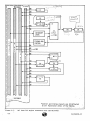
TM
PUBLICATIONS
TO DP IM
x
x
x
x
x
x
x
x
x
x
x
x
x
x
POWER SUPPLY
SMALL I/0 BOARD
MEMORY OR I/0 BOARD
I/0 BOARD
MEMORY OR I/0 BOARD
14
MEMORY OR I/0 BOARD
13
MEMORY OR I/0 BOARD
12
MEMORY OR I/O BOARD
I/0 BOARD )( l l
OR
. OPTION
MEMORY OR I/0 BOARD
10
MEMORY OR I/0 BOARD
9
MEMORY OR I/O BOARD
8
MEMORY OR 1/0 BOARD OR OPTION
7
MEMORY OR 1/0 BOARD OR OPTION
6
OPTION
-
~
.l>-5
....~1-----<
*
EMULATE BOARD
- Io
1--------------------c
4 ENGINE BOARD 1
.... ; 8' o
--
x
x
I
18
17
16
15
...._MEMORY
x
x
x
I
-
x
x
x
Q)
UM
SYSTEM HARDWARE
r
~
ENGINE BOARD 2
MACROBUS CHANNEL ADAPTER
MACROPANEL
3
....
~i------<
--
2
1
._ I q o
- ":) C'>O
-3 ltO
\.
x
x --x ....~1-------
x
..J
Computer·System
Engine Microprogramming
NOTES:
A Standard 18-Slot Backplane is Shown
•
.
'.~
'\,
~
:
I
1
* = MACROBUS Tenninat'6t· 1Qr Extension Cable
JA,
''
CD
TM = Technical _Manual
TO = Theory of Operation
.:'.
DP = Ehgi neeri ng Drawing Package: ... ~.' ·,,.
IM = Installation .Manual
· UM = User Manual
Figure 1-1.. Relationship of Publications to Ca~:Data·l System Elements
1-2
..
..
c21s1aooa.:..xo
1. 2. 3
Abbreviations and Conventions
Tallle 1-1 lists the abbreviations foun.d in this manual.
used in the text of this manual include:
a.
b.
c.
d.
e.
C21518008-XO
Conventions
Equipment panel nomenclature is reproduced in
all upper-case characters.
The proper names of instructions, microcommands
and signals are capitalized.
ZERO and ONE are used to express binary logic
"O" and "l" states, respectively.
Hexadecimal numbers are preceded by a dollar sign
for easy identification.
A colon is used to indicate a range of bits. For
example, the range of address bits Al2 to A03 is
written Al2:A03.
1-3
Table 1-1.
·Abbreviations
Abbreviation
Cal Data
CPU
MCA
I/O
LFC
RAM
ROM
PROM
MSI
LSI
MMU
LED
ACM
DMA
CM
cc
CR
cs
SC
LC
MB
FR
AB
BB
AU
sx
PS
LR
RR
IR
XR
ER
EIA
c
.v
z
n
p
d
1-4
Meaning
California Data
Processors
central processi.ng unit
(engine)
MACROBUS Channel Adapter
input/output
Line-Frequency Clock
random-access memory
read-only memory
progrannnable read-only
memory
medium-scale integration
large-scale integration
Memory Management Unit
light emitting diode
Alterable Control Memory
direct memory access
control memory
microcommand location
counter
microcommand register
control stack
stack counter
loop counter
M bus (data destination
bus)*
file register
' A-operand bus*
B-operand bus*
arithmetic/logic unit
AU shift elements
processor (macro)status
register
stack-limit register
data-read register
instruction register
shift.register
emulate decode register
emulate instruction address
carry out
microcondition code
overflow
microcondition code
zero data-value
(microcondition) code
negative ;~data-value
(mic~o-cQndi tion) code
positive Ciata-value
(microcondition) code
odd data-value
(microcondition) code
Abbreviation
MS
L
v
z
N
p
D
cps
cpm
lpm
K
max
min
A
ac
de
nns
v
ns
Hz
oc
cm
*
...
Meaning
microstatus register
MS register
link bit
MS register
overflow bit
MS register
zero data-value bit
MS register
negative data-value bit
MS register positive
data-value bit
MS register odd datavalue bit
characters per second
cards per minute
l~nes per minute
l,024(address or
memory locations)
maximum
minimum
ampere
alternating current
direct current
root-mean-square
volt
nanosecond
hertz
degrees celsius
centimeter
= part of the main Microbus
c21s1aoooa.:..xo·
SECTION 2
DESCRIPTION
2. 1
OVERVIEW
The Cal Data 1 Computer (Figure 2-1) is a high-speed microprogrannned
digital computer designed for application in a wide variety of computing
and control applications. Microprogrannning, combined with a powerful ·
and flexible hardware architecture, centering around the Cal Data 100
Engine and Microbus, permits the basic computer to be fully optimized to
a specific application. The Cal Data 100 Engine is designed primarily
for efficient, high-speed emulation of general-purpose computer architectures. It can also be applied as a direct function processor by implementation of problem-oriented microprograms.
2.2
SYSTEM ORGANIZATION
The overall system organization is shown in Figure 2-2. The system
consists of a set of hardware and software elements that can be utilized
in a wide variety of applications. A brief description of the elements
of the computer system is given below. Details are given in other sections of this manual and in supporting manuals.
2.2.1
Engine
The central element of the system is the ~ngine (CPU), divided into con-.
trol and data sections, and controlled by microprogram sequences (firmware) stored in a control memory. By changing the contents of control
memory, the entire operation of the system can be altered. An emulation
system is implemented by placing appropriate firmware in control memory,
causing the CPU to operate like the computer being emulated.
The control and data sections contain the internal arithmetic/logic circuits, data paths, registers, control logic and timing circuitry of the
machine. The CPU communicates with the rest of the system via the
Microbus.
2.2.2
Microbus
The Microbus is a universal bus that is the main connnunication and control channel of the system. The Microbus transmits data and control information between the CPU and all elements of the system.
The Microbus can be conditioned by one or more I/O channel adapters to
interface with a wide variety of I/O devices obeying specific interface
rules. The primary I/O channel adapter o~ the Cal Data 1 system is the
Cal Data 1 MACROBUS Channel Adapter.
MACROBUS Chagnel Adapter
~
·~
The MACROBUS Channel .Adapter (MCA) provides data, address and control
circuitry for parallel I/O operations in the system. The McA frees the
·c21s1aooa-xo
2-1
!
Figure 2-1. Cal Data 1 Computer System with Memory Management Unit, 128K Words·.
of Cal D~.!:a 16KX16 (850-ns) Core Memory and Serial I/O Controller
2-2
: C21518008-X.Q>
.
MACRO BUS
TERMINATOR:
SERIAL 1/0
CHANNEL
MACRO PANEL
.,.___ _ _ _ M_ _ _ ___.
MACR~BUS
CHANNEL ADAPTE R
A
MEMORY-MANAGEMENT
0
c
J
R
_!l_N!L _ _
t
B
u
1.,..,-1
-----M-------11
....__ _ _ _ A_ _ _ ___.
c
MICROCONSOLE _j.
----
R
•
----
-,-,---
L.-1
1/0 CHANNEL #N
MACROBUS
TERMINATOR
MICROBUS
. COMMUNICATION
·CHANNEL AND
INTERNAL CONTROL
- - =Optional
Cal Data 1 Computer System
PERIPHERAL
CONTROLLER
s
lt"o~HANNa I
ADAPTER #N _j
C2151800S-XO
•
------,
B- - - -..---11
u-------11
-----
2-2.
MEMORY
0
------,
SPECIAL
I
FUNCTIONS _j
'.f igJ;~
_j
•
----,
·~OTE:
----
PERIPHERAL
CONTROLLER
ENGINE
BOARD 2
EMULATE
BOARD
l/o-i_J
5E°RIAL
CONTROLLER
s
ENGINE
BOARD 1
Organ~zation
t
SYSTEM
I
INTERFACES _J
central Microbus for very-high-speed communication between the CPU and
other Microbus devices, and can permit I/O channel devices to communicate
directly with each other, independently of the CPU.
2.2.4
Macropanel
A Macropanel, representing the control panel of a general-purpose computer, is often provided in an emulation application. The Macropanel is
serviced by the CPU as an I/O device interfacing with the MACROBUS.
Special support firmware is provided for the Macropanel. The primary
Macropanel for the Cal Data 1 system is the Cal Data 1 Macropanel.
2.2.5
Microconsole
A Microconsole is available to provide microlevel control and display
for checking out and debugging firmware, and also for various maintenance and troubleshooting procedures. The Microconsole consists of a
remotely mounted Micropanel and a plug-in Micropanel ~ontrol board that
permits the user to exercise direct control over· the CPU. Facilities
are provided to construct full microcommands, to display microcommands
and to execute microconunands on a single-step or "trap-mode" basis.
The Microconsole also contains 32 words of alterable control memory
that can substitute for equivalent blocks of CPU control memory.
The Microconsole can be used in conjunction with the Macropanel and is
useful for initial debugging of new firmware as well as for on-line
troubleshooting of computer hardware, but is usually not required in an
applied system configuration.
2.2.6
Magnetic Core Memory
Cal Data core meIOC>ry comprises modular blocks of SK (8,192) or lGK
16-bit words, each contained on a single circuit board. Each module
plugs directly into the MACROBUS and is treated as an I/O device in the
system. The maximmn normal system capacity is 128K words. Two identical modules can be interleaved to achieve an increased effective throughput rate on the MACROBUS.
The MACROBUS can accommodate memory devices other than magnetic core,
such as semiconductor ROM or RAM modules.. The only requirement is that
such units obey MACROBUS use rules. Modules of varying size and speed
can be freely mixed with core memory. OMA-type MACROBUS devices may
communicate directly with memory.
2.2.7
Peripheral Devices
Peripheral device controllers and system interfaces are attached to the
MACROBUS as shown,; in Figure 2-2. The user can readily interface devices
·;."·.with'tthe MACROBQS.. 'Using simple design rules. Cal Data offers I/O channels
· .. su~h as tne MACRbBUS with different structures as well as several. ~itandard
periph~r~l "sub'sy'stems to enhance user applications.' The subsyste~s
·. ·
offer~d 'to" support· normal progranuning and system development operations· ·
·are:
·c21s 1aooa-xo
a.
b.
c.
d.
e.
2.3
Paper Tape Reader. High-speed photoelectric reader, 300
characters per second, fanfold tape.
Paper Tape Punch. High-speed punch, 75 characters per
second, fanfold tape.
Card Reader. High-speed photoelectric card reader, 300
cards per minute with code conversion in the controller.
Line Printer. 80- or 132-column printer, 125 or 200
lines per minute.
Memory extensions.
FIRMWARE DEVELOPMENT AIDS
Cal Data offers specialized hardware and software elements to aid users
in developing custom firmware. These are briefly described below.
2.3.1
Alterable Control Memory
Alterable Control Memory (ACM) is a modular plug-in unit that contains
increments of 256 words of electrically alterable control memory. The
ACM also contains alterable elements associated with instruction emulation and decoding.
With the ACM, a programmer can load or read the contents of control
memory directly and execute trial firmware code at normal processor
execution speeds. The ACM is particularly useful for dynamic system
tests where external real-time events must be considered to fully evaluate a firmware microprogram. The ACM is supported by a software operating system that permits the programmer to use a teleprinter to control
the system.
2.3.2
Support Software
The following software is available to support firmware development:
a. Symbolic Microassembler. This program is a complete
symbolic assembler that permits convenient coding and
listing of microprograms. It is written in Cal Data 135
emulator language and can be run on any Cal Data 135 or
compatible computer having the required memory configuration.
b. ACM Software Operating System. This program is designed
to provide operational control over execution of firmware in the ACM. It requires that the Cal Data 135
emulator be resident in control memory.
2 •.4·
FEATURES
The Cal Data computer architecture combines general microprogranuning
capability with specialized optional features. to . permit higp
emu.lation
.'
' ' ~ .
speeds with efficient control-memory space utilization. The~· meCnanical
design used prov~des full modularity, mounting ii.~xibi'l:i:t;:y' .and service
convenience. Cooling, power distribution arid dtllefr · crl.tlcal system requirements are optimized for OEM applications~ Conser'7ative el.ectrical
"implementation ensures wide margins, readily available components and
reliable operation over a.wide environmental range. Subassemblies are
'
·c2151sooa:..xo.
des_igned for easy assembly and automated testi_ng, and the overall system
is structured for simple, straightforward manufactur~ng procedures.
Basic des_ign features of the Cal Data computer system are:
•
•
•
•
•
•
•
•
•
48-bit microconunand word length
Parallel execution of multiple functions per microcommand
165-ns microcommand execution time
16-bit data word length
16 multipurpose file registers (16 bits each)
Nine additional registers accessible by microcozmnand
16-level hardware pushdown stack
Microcommand sequence repeat loop counter
Optional high-speed emulation instruction decode, function
generation and interrupt-response hardware.
Bit, byte and word manipulations
256- to 4096-word control memory using bipolar ROM or PROM devices
Power-failure/restart circuitry and line-frequency clock included
in the computer
Unique, control memory substitution provisions
Optional Multiply, Divide, and single- and double-precision Shift
micro commands
Hardware microprogram interrupts
•
•
•
•
•
•
Input/Output and Memory
•
Universal asynchronous I/O channel with direct-memory-access
capability
Four external priority interrupt levels
16-bit parallel· word or byte-mode transfers
Automatic I/O channel delay time-out protection
Optional asynchronous serial I/O channel
BK-word (675-ns cycle, 275-ns access) and 16K-word (850-ns cycle,
300-ns access) core memory modules
Interleaved data transfers between identical memory modules
Optional extended addressing feature for addressable memory expansion to 31K without memory management
Expansion to 124K or 127K of directly addressable memory with
optional. Memory Management Unit
•
•
•
•
•
e
•
•
Microprogramming Aids
•
•
•
Microconsole
Alterable.Control-Memory and support software
Symbolic . .Microassembler
Packaging, Pbwer and Environmental
• .
10~
inch coinputer chassis with vertical board mounting from the top
~.-'•,.
,~;~>:P:finted-c;i.rcui
t backplane with up to 13 spare slots for memory and
.. .
•.-:;·.:
,,.
·;
:>. •,. .
•
......'Ir
,
;'2.~6.
·~:.~,(...Q~6P...'l.t:ro.~ler
boards
.'Fd'ui:W';6ans" for high-volume, positive-pressure q.ir flow throuqh the
· 'cih'cl:S~i~~·rwith provision for air filters
._·~ ..,
Modulaf~ p0wer supply providing 36 A at +5 Vdc
c2151aoba!.~o
:
•
•
•
•
•
•
Low-noise internal power distribution and grounding system
Convenient external I/O cabling
Extension chassis available
System designed to meet UL standards
O to +5o 0 c ambient operating temperature
10 to 90% relative humidity (without condensation)
Electrical and Electronic
•
•
e
•
•
•
•
2.5
Bipolar TTL integrated circuits (multisourced)
Extensive use of MSI and LSI
Wide timing margins
High noise immunity I/O drivers and receivers
Single-phase clock
Conservative component derating
Metal can transistors and hermetically-sealed passive devices only
SPECIFICATIONS
.General specifications for the Cal Data 1 Computer are given in Table 2-1.
Table 2-1.
Cal Data 1 Computer Specifications
Characteristic
Specification
TYPE
High-speed microprogrammed digital computer designed for efficient emulation
of general-purpose computer architectures
and for direct custom applications
CONTROL
Microconunand length
48 bits
Execution rate
165 ns, min.; 330 ns if skip or branch
is made; clock rate is adjustable
Microcommand classes
8 arithmetic
16 logical
8 special
Special operations
Special microcommands include doubleprecision Shift, Multiply-Step and
Divide-Step
·
Conditional
skip/branch
Each microcommand wi,th conditional skip
or branch capabilit:Y"r ~ests on either
current {dynamic) c.onditions or
on previous {static} conditions
Fixed control memory
Bipolar ROM or PROM; 4, 096.,.wqrds, max
- .':L . ~ .~ ?:.'.:'._:f . . ·:'.:~y /
Bipolar RAM; 512 .wor~r ~·'..without .
auxiliary power; i,'s§6:tf;;d:ids·
max' ·with·.-· ..
••
'' l'." .; • . auxiliary power. ,'°\?. ""·:·Y·
:
.·Alterable control
. _memory
' i( ...~.. - j
. _': C2?5:1'8008~X6
··~
Table 2-1.
(Continued)
Characteristic
Control memory stack
16-level hardware pushdown stack
Emulation enhancement
Special emulation decode tables provide
automatic addresses to control memory
microroutines for high-speed program
execution
Loop counter
Eight-bit counter for single or multiinstruction repeats
Interrupts
Multilevel priority-interrupt structure
provides automatic addresses to control
memory microroutines for internal and
external conditions
PROCESSING
Word length
~.·:.<
:. '' ~-
16 bits
Arithmetic/logic
Both word and byte operations are provided; fixed point, one's or two's
complement arithmetic; arithmetic
condition codes are carry (link) , overflow, negati:_ve, zero, positive, odd;
arithmetic~and logical shifts (multibit
using loop counter for repeats are
provided)
Registers
Eight or sixteen 16-bit multipurpose
files (FR)
Shift register (XR)
Microstatus register (MS)
Instruction register (IR)*
Decode Register (ER)*.
Processor (macrolevel) status register
(PS)*
INPUT/OUTPUT (TYPICAL)
Type
'
Specification
I;)at·a
Asynchronous bidirectional I/O channel
derived from the Microbus; requires I/O
channel adapter; handles communications
between CPU, memory and peripheral
elements
16 bits with byte capability
... .-·
16 bits from Microbus (can be.extended
within I/O channel adapter);ieastsignificant bit is for ~yt{addressing
..
*Part of emulation enhancement circuitry
.,i
}
i.,
·1.
'. ~.
,,.·,.
i/_:_.__ Y·
Table 2-1.
(Continued)
Characteristic
Specification
I/O channel
priorities and
requests
Four priority-request levels with
multiple requests per level;
nonprocessor request (NPR) level for
direct device-to-device transfers;
CPU can set its own priority to any
level except NPR
Serial I/O channel
Serial I/O controller (option) for
rates up to 9600 baud; RS-232 or current-loop interface
Memory
Magnetic core; SK or 16K words per
module; 16 bits per word
Memory expansion
Typically, 124K words maximum; Memory
Management Unit (option) is required
above 32K
Memory interleave
SK-word or 16K-word Cal Data core memory pairs can be interleaved for increased throughput rate
Line-frequency
clock
50/60
PACKAGING
Processor chassis
Hz
line clock
10~
inches (26.7 cm) high by 19 inches
(4S cm) wide by 24 inches (43 cm) deep;
rack-mounted (slides) or table-top;
vertical, top-loaded boards; contains
Macropanel, Engine, MCA plus slots for
memory and I/O controllers; internal
power supply; cooling fans; internal
power distribution
Connectors
36-pin, 0.6 inch (1.5 cm) card insertion depth; mounted on printed-circuit
backplane
Board size
S.9 by 15.7 inches (22.7 by 39.9 cm);
six connector positions (216 pins) on
long edge
POWER
AC input·
115/20S/230 Vac, 50 or 60 Hg
.
Regulated:
• I
·~ ~~'~·~\~ ),~~~<·•
•
+5 Vdc, 36- A .:,' .
-15 Vdc, 12 ·.A.- .' ·..
'c21518008-Xff
j
·~'/·
Table 2-1.
(Continued)
Characteristic
Specification
Unregulated:
Power monitor
ENVIRONMENT
Temperature
Humidity
CIRCUITS
Integrated circuits
-22 Vdc, 1.5 A
+8 Vrms, 1.5 A
Power-failure/restart signals to CPU
for automatic shutdown and restart
operations
o0
to·+so 0 c ambient temperature
10 to 90% relative, without condensation
Bipolar TTL; extensive MSI and LSI
usage
Discrete devices
Metal-can transistors; hermetically
sealed components only
Internal logic levels
ZERO = 0 Vdc; ONE = +5 Vdc, nominal
I/O logic levels
ZERO
= +3.4
Vdc, nominal; ONE
=0
Vdc
MICROPROGRAMMING
SUPPORT HARDWARE
Microconsole
Alterable control
memory (ACM)
Provides direct control over Engine;
microcommand entry and display;
single-step and trap-mode microcomrnand execution
Modular 256-word increments of control
memory that can be loaded and read;
operates CPU at full execution speed
MICROPROG~ING
SUPPORT SOFTwARE/
FIRMWARE
Symbolic·· microassembler
'
ACM software
operating system
2~10 "
Symbolic assembler for microprogram
coding and documentation
Operating system used in conjunction
with ACM
SECTION 3
PHYSICAL DESCRIPTION
3.1
SYSTEM HARDWARE
All Cal Data Engine and system elements are modular and can be mounted
in a standard chassis (Figure 3-1) that occupies 10.5 inches (26.7 cm)
of a 19-inch (48-cm) RETMA rack. This modularity gives the user
maximum flexibility in system design and configuration.
The standard computer chassis dimensions are:
10.4 inches (26.5 cm) high
19.0 inches (48.3 cm) wide
24.0 inches (61.0 cm) deep
Hardware items included with the standard computer chassis are:
a. Chassis box with backplane
b. Top and bottom covers
c. Hinged fan panel and four fans
d. Chassis slides
e. Macropanel bezel and overlay
A power supply mounts at the rear of the chassis. The ac power cord
exits from a control panel accessible at the rear of the chassis. This
panel also has the ac line switch, fuses, convenience outlet (115 Vac
model only) and Macropanel lock switch.
The four fans provide horizontal, positive-pressure air flow across the
vertical computer boards and power supply. The fan panel is hinged
to permit moving the fans when boards are removed or installed.
System electronics are mounted on modular printed-circuit boards that
insert vertically through the top of the chassis into connectors
mounted on the backplane in the bottom of the chassis. The backplane
provides printed-circuit (and wire-wrap) connections between all
boards.
Device controller cables are generally connected at the top edge of I/O
boards by means of flat cable. These cables a¥e routed over the top
of the boards and exit via a cutout at the top'.. rear of the chassis.
A strain-relief clamp is provided. All standard Ca1:Data I/O
and memory boards have provision for this cable routing scheme. The
backplane contains up to 18 connector rows ~bo~rd slots).
The Macropanel is mounted on a printed circuit board that plugs into the
first connector row of the backplane. The Macropanel is covered by·':··an,
overlay held in place by the bezel. The bezel and over.l,ay ·are
·· ·
removable.from the front when the chassis is install~d :i;n~~ ra9k.
C21518008-XO
3-il.
Figure 3-1.
Cal Data 1 Computer with Boards Installed (Fan Panel is Shown Down)
3.2
ENGINE BOARDS
The Engine comprises two boards labeled Engine 1 (part number C81080180)
and Engine 2 (part number C81080190). Each Engine board (Figure 3-2)
is a hex-width board 15.7 by 8.9 inches (33.9 by 22.7 cm). Engine 1
nonnally plugs into slot 4 of the cal Data computer chassis.~ Engine 2
nonnally plugs into slot 3. The right-hand edge of each b~ard has
a 1.0 by 5.5 inch (2.5 by 14.0 cm) cutout as clearance for the sidemounted cooling fans in the chassis.
There are six printed-circuit connectors (A to F) on the bottom edge of
each board, and two (Jl and J2) on the top edge. Connectors A.and B
interface with the MACROBUS. Connectors c to F, and Jl and J2 interface with the main computer Microb.us~ , Connectors A to F are standard
backplane connectors. Connectors Jl and J2 plug into the two small
processor-interconnection boards.
There are no controls or adjustable elements on the Engine.
*Because· of tjl~ universal connections in the CPU area of the chassis, the Engine
.. boards . can op~~ate ; in any slot from 1 to 5.
· c21s1aooa.._..xo.
15.69"
0.99"~
A3o--------------------
Al
a
J2
Al
a
a
l-
©
Jl
an
an
.
an
COMPONENT SIDE
FVl
FAl
·®Solder Side
.·~@) so·l der
'NOTES:.:
· :, ·. Figure 3-2.
.·.· 3-4'
EAl
EVl
= Bl
DVl
DAl
CVl
CAl
BVl
BAl AVl
CD
'd'
°'ClO.
AAl
to 830. Likewise with connector.J2 •
Si de = AV2 to AA2. Likewise with connectors B to F.
.
Cal Data 100 Engine Board Configuration
···c2i.s1eooa-xo
SECTION 4
ENGINE
' 4.1
FUNCTIONAL DESCRIPTION
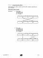
Figure 4-1 is a block diagram of the Cal Data 100 Engine, showing three
main functional sections: control, data and MCA. The control section
contains the control memory, emulation enhancement circuitry (if
needed) and timing circuits that control the sequence of operations
performed. Emulation enhancement circuitry is provided only when a
computer configuration requires the speed or special capabilities of
the added circuitry. The data section contains the arithmetic/logic,
gating and busing elements that perform data transfers and manipulations. The basic control and data sections together are referred to as
the Engine or CPU. The main communication path in the.computer is
the ~:t:_QQ!!s, used for parallel transfers of information and control
signals between the CPU and all functional system elements. The
microbus comprises the A-operand bus (AB) , th.~_ B=_qperand bus (lm) ,
the
~-p-~_(MB) and other- li"IleS--(Appenaix A)~- The Engine and all
~
'---external devices, including memory, Macropanel and peripherals
communicate with the Microbus. The relationship of the Microbus and
Engine logic is illsutrated in.Figure 4-2. Certain Microbus functions
can be perfonned by the MCA for common I/O devices, allowing the
Microbus to attend to higher-speed units. Devices on the MACROBUS
can communicate with the CPU and directly with other devices, depending
on their design. The MCA is shown in Figure 4-1 because of its
important function of conditioning the Microbus for use by the mass of
common peripheral devices.
A basic MACROBUS device is the magnetic core memory, which is generally
required in any system. Cal Data core memory modules are available in
8K- and 16K-word increments and can be added directly to the MACROBUS
up to a typical maximum of 128K words*.
Semiconductor memory can be interchanged with core in any speed/
capacity mix. The CPU addresses memory locations like any other _I/O
devices.
Two types of control panels are available: a Macropanel that is
adapted to a particular emulation and permits the ope11ator to control
the system at the emulated level of operation, and a Microconsole that
permits control and display at the microlevel and is useful for firmware
development, hardware maintenance and troubleshoo~ng. The Macropanel
is treated as an I/O device. Special interpretive_firmware services the
functions of the Macropanel.
*Maximum memory·c~pacity.of the basic system is 32K words. A Cal Data Memory
Managerttent Unit-is required for expansion beyond this capacity.
: C21518008-XO,· :
'I\
I
INTERRUPT
LOGIC
SC
IE cc
M
B
CM
CR
u
s
SELECTOR
CONTROL
_ _ _SECTIO_N-~
DATA
SECTION
FR
BB
AU
NOTE: ~
Figure 4-1.
=
AB
(A-OPERAND BUS) SOURCES.
Cal Data 100 Engine Block Diagram
(continued)
'C21518008-XO
@
_ _ _ _ _ _ ____,.AM
EMULATE
TABLES
B
M
"4---
c
----+---r----11-.. SELECT
GATES
B
u
s
ps
I
ID MS >~ -it-YL
(PARTIAL) -tt-p-
I
R
I["
0
B
.
,<I'.,,..,,_
fYlt1"~t//.r.' .•~4.. !.i._v,:..
su
;::t.J-/'.·
CONTROL SECTION
EMULATION ENHANCEMENT
~'
MACRO BUS
CHANNEL ADAPTER
(NOT PART OF ENGINE)
AR II
---AL
MACROBUS
CONTROL
LOGIC
DR to
--DL
MACROBUS ·\'"
PRIORITY
OGIC
MACROBUS
I
...
Figure 4-1.
..
. (Continued)
;
C215180b8-:XO
4-3
,"f,.,. .-- .... 'l'.7;:/
d'-G ,'rs)
\_.
--:.r
----'I
If
CS::~;~~...._,............
I 1d
t·t~
cc
INTERRUPT
LOGIC
BB
BB
AB
~...........,....,.___,.,...,....,..._-+-_..,.
P. f,Il
1~l-·X-c:rrl
C--1'-''·H~
ONE
sx
·,e---t---~F1J..c... A.ca
FR
... .
.....,.....
i,i.,.,
'.ii·,~..
er •
*Control and timing sign.als are ,di.stributed
to all functional areas o~ the·.::E~gjne .. ·
':·'··. -...~~:.-'~·.:.~~;!:: ..
·piqure 4-2.
Cal Data 100 Engine Interface with the Microbus
.···:'.'.
4.2
CONTROL SECTION
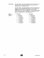
A block diagram of the control section is shown in Figure 4-3. Control
is organized around the control memory (CM), which stores the microprograms to be executed. Microcommands are 48 bits in length. Normal
CM'capacity is from 256 to 4,096 words (48 bits each).
A 12-bit location counter (CC) addresses CM and advances on each clock
step unless altered by a sequenc~ cha._nge. Microconunands read from CM
are held in a microcommand register (CR) during execution. The microcommands read from CM can be.. m0dified prior to input to CR for execution. Microcommands can also be entered manually into CR and executed
from the Microconsole (not shown).
A 16-level control stack (CS) is provided to permit the contents of CC
to be saved and restored under microprogram control. This permits
automatic nesting of microroutines and microprogram interrupts, giving
increased speed and ~~ space efficiency. Th~-- --~ys_tem contains a unique
f~~~!3-.tY__ tha1: _permit~ def:>ign~ted are~s of_CM_to. . l.?~.-"Pc;t_c;l}_~g_'~--~~QI.Il_ ~~=ilia~CM .. or __ from ____tlle___ ~-~~C?~~~sole •. This is a highly useful feature,
since nonalterable storage elements are generally used to implement CM.
An eight-bit loop counter (LC) is provided to permit single microcommands or entire sequences to be repeated a specified number of times.
This feature enhances execution speed of iterative loops.
A special feature of the Cal Data 100 Engine is emulation enhancement
circuitry, located on a separate Emulate Board. This circuitry provides:
a. Automatic table-generated addresses :to CC to steer the microprogram directly to specific emulation microroutines, by-passing
lengthy processing to decode instruction codes and addressing
modes
b. Automatic interrupt microroutine location entry to CC
c. Automatic table-generated modifiers to microcommands read from ·
CM
d. Automatic modification of processor status conditions for the
emulated instruction
e. Direct designation of word or byte-mode operations
Emulation-related features are described in a separ.ate emulation user
manual, available for each computer m~del.
4.2.1
Control Memory (CM)
The control memory is a high-speed, random-access unit. Three device
implementations can be used:
a. Read-only memory (ROM). These bipolar semiconductor devices
are organized on chips of four by 256 (or f~ur by 512) bit·5·: . ;
Twelve such devices implement each 256-word (or 512-~ord) CM~
page. The code pattern in each chip is permanently inscribea
during the factory manufacturing process and cannot b'e altered.
~OM is used for high-volume' production of fully debugged firmware.
C21518008-X0°
~
I
°'
~
.....
's=°
t;
Cl)
~
.w
I
STACK
COUNTER
(SC)
M
()
p.i
......
B
0
u
p.i
rt
p.i
CCll:CCOO
s
LOOP
COUNTER
(LC)
......
0
0
l:Ij
!:1,
CCll :CCOO
CONTROL
STACK
(CS)
CSll: CSOO
CONTROL
MEMORY
(CM)
t.Q
.....
MICROCOMMAND
LOCATION
COUNTER
(CC)
MBll :MBOO
!:1
Cl)
()
0
!:1
rt.
t;
0
~
......
c:n
Cl)
()
MACROBUS INTERRUPT
rt
.....
INTERRUPT
PRIORITY
LOGIC
INTERRUPT
ENTRY
TABLE (ROM)
EIA07:
EIAOO
MCA
0
CRll : " - - - -..........
CROO
. !:1
tJj
......
0
()
.· 7;"'
...
~
p.i
t.Q
t;
·~
EMULATION
ENHANCEMENT
CIRCUITRY
EMULATE INSTRUCTION
ADDRESS
EIA08: EIAOO
SELECTED
CM47:CMOO MICROCOMMAND
1---:~~-------1~ REG I ST ER
CM BITS
(CR)
11
- -
<
'
()'
tv
........
. 00
0
0
00
I
x
0
Note:
~
=
provides signals to
the A-operand bus
(see figure 4-4).
0NE
11
SELECTOR
____....
CR15:
CROO .._
CR47:
CROO
, . . . I-"
.
l11
CM47:CMOO
TIMING
AND
CONTROL
CM47:CMOO
BB15:
BBOO
........_~
DATA
SECTION
INTERNAL TIMING
AND CONTROL
SIGNALS ·
b.
c.
Programmable read-only memory (PROM). These bipolar semiconductor devices are organized on chips of four by 256 bits,
pin- and speed-compatible with the equivalent ROM. The code
pattern in each device is electrically and permanently inscribed by a portable programming device. ~M_is_used_fo~
development and_J_ield..debugging.. _of .. firmware and also for low'Verlline production firmware packages.
Alterable Control Memory (ACM). The Cal Data AOvl is a complete,
modular control memory that can be installed in the computer in
addition to or in place of ROM and PROM devices. It is implemented with bipolar random-access memory devices that can be
electrically altered (read/write). When installed in the computer, ACM can be loaded and read via the MACROBUS using I/O
microconnnands. The ACM can then take control of the CPU for
execution of ACM firmware at real-time processor speeds. The
ACM is most useful for initial and on-line checkout of new firmware prior to conversion to ROM or PROM devices.
The normal maximum capacity of CM is 4K words* when ROM or PROM devices
are used. Although each microconunand is 48 bits in length, the CM addressing structure of the microcormnand limits direct access to 2K words;
however, a paging scheme between 2K-word blocks permits convenient access anywhere within 4K words.
Auxiliary Control Memory. It is often desirable to alter the contents
of CM, either temporarily or permanently. When nonalterable devices
are used, the usual requirement is replacement of the existing devices.
The Cal Data loq Engine incorporates circuitry that permits either one
or two 32-word blocks of auxiliary memory in. the Microconsole to functionally replace designated 32-word blocks in CM. This enables
"patching" for corrections, additions or deletions from existing firmware, temporary overlay for diagnostic and troubleshooting operations,
etc.
4.2.2
Location Counter {CC)
The location counter is a 12-bit binary counter/register that points to
the location in CM of the next rnicroconunand to be executed. The microprogram sequence can be altered conditionally or unconditionally as
specified by the programmer and the state of the system. A sequence
change is made by loading CC from one of the following sources:
a. CR for programme~ branches
b. M bus for compu_ted branches
c. The current CS,register
d. A vector from the emulation enhancement circuitry
e. An interrupt v,ector
CC normally advances sequentially to the· next location through all.4K
locations in CM, including the wrap-around transition from 4,095 to O, ..
unless the normal sequence is altered.
*Auxiliary ·power. is· 'required above 512 words.
C21518008-XO
4-7
CC modifiers from CR and the emulation enhancement circuitry are 11 bits
long, permitting branches to occur from these sources within only a 2Kword area. The most significant bit of CC is unaltered for such
branches. To branch to a location outside a 2K-word area, the programmer must execute a microcomrnand that transfers a full 12-bit branch address via MB. Interrupt vectors are to only the first 256 CM locations
(i.e., the four most-significant cc bits are forced to ZERO).
Certain conditions cause an automatic reset of CC to location O (a corresponding microstatus bit is set for each condition) :
a. A catastrophic system error
b. A power-up sequence
The contents of CC can be read by microcomrnand via AB. For systems
that do not contain an implemented CS, this provides a means of saving
a return location in CM.
·
4.2.3
Microcommand Register (CR)
The 48-bit CR stores the current microcommand read from CM for execution.
The'microcomrnand from CM can be modified prior to entry into CR by a
function specified by the special decode circuitry on the Emulate Boar~.
CR can also be loaded from the Microconsole to permit direct operator
control of internal functions. The least-significant 11 bits of CR ·
modify CC when a branch operation is specified by the microcommand in
CR.
Microcornrnand Sequencing and Timing. The basic clock cycle is 165 ns
(adjustable) and, ordinarily, a microcommand is read from CM and 'executed on each cycle. There is a one-clock delay between the time CC
addresses a word in CM and the time that the microcomrnand is transferred
to CR for execution. For this reason, when the·n~i:-rnal CC counting sequence is modified, two clock cycles are required to a~cess the microcornmand at the branch location and transfer it to CR~ Furthermore, the
microcomrnand accessed at the time CC is modified is transferred to CR
even though a branch is being made. Whether or not this "extra" microcomrnand is executed can be specified by the programmer. The following
sequence illustrates the operation:
Time
cc
CR
T-1
T.
_'J:'+l
T+2
X.
(X-1)
X+l
y
Y+l
no
(X1:_1)
(Y)
Operation
I
Branch to Y specified
Microcomrnand at X+l can be executed
Micro command at branch location
In addition to sequence modification, the programmer can specify· that
.t~e succ~edin·g microconunand be skipped. · In this case, the succeeding
microc~~and is· transferred to CR, but execution is inhibited.
Th~s
action. is not considered to be a sequence change since CC continues
normal sequential counting.
.
The output of CR is decoded to generate the timing and control signals
used throughout the computer.
4-8
c21~1aooa~xo·
.
.
.
~
'
'
Depending on the microcommand, the least-significant 16 bits of CR can
be gated via BB into AU. Alternately, a literal "one" value can be'."'
placed on BB.
4.2.4
Control Stack (CS)
cs
contains 16 12-bit registers. that are accessed via the four-bit up/
down stack 'counter (SC)·. When a CC "save" is specified by a microcommand, 'the contents ,of CC are transferred to CS. The contents of CC
are always one greater than the location of the microcommand specifying
the save •. Likewise, a microcommand can specify a return operation that
transfers the contents of the current CS location to cc. The return
microcommand can simultaneously transfer the (incremented) contents of
cc to the cs register that contained the return address. Incrementing
and decrementing of SC can be specified independently of the save and
return functions. CS permits convenient implementation of re-entrant
and multi level subroutin.es-at-:the._mi_9rq_:t_~e.l.. Any microcommand branch
condition can specify a save operatIOn with an automatic return to the
calling sequence using a Return microconnnand.
SC co.unts up from zero, modulo 16, and "rolls over" the boundary in
either direction. There ~§_)]._<?__ !_~4J.ccition given for a._ stack ove.rflow.
It is the pro_g;:aIT1Iller' s .:r;esponsibili ty to maintain the stack within
-l-i1n.t-t:s:-- . -------·- -·
--~··---··· ......
. The contents of CS (current location) can be read by microcommand;
.however, Cp cannot be directly loade4 and SC is not directly accessible
to the microprogram. The contents of CS, therefore, cannot be saved in
the event of a power interruptiqn. It is mandatory that provision be
made to execute all returns in ·cs within the" time available for power
interruption. Since several milliseconds are available, this imposes
no practical restriction on the use of the stack~
4.2.5
Loop Counter (LC)
A powerful feature of the Cal Data Engine is the eight-bit LC that permits a single microcommand or a group of microcommands to be automatically repeated up to 256 times. LC is loaded via MB and can be read
with a microcommand. In a repeat sequence, LC can be tested
' :, .. for a zero
or nonzero condition by any microcommand in the sequence.;1... with a branch
operation executed if the condition is met. LC is decreni~nt~d each time
it is tested. Individual microcommands can also be repeated the number
of times specified by LC.
'
4.3
DATA SECTION
A block diagram of the data section is shown in.Figure 4-4. The ~ata
section contains the basic arithmetic, logic and busing elements of the
Engine required. for manipulation and transfer of da~a throughout .:t;:he
computer.
:.~21.s1aoaa~xo
4-9'
....
1-:tj
~
I
.....
0
l~
~
.
I'
~
()
Ill
.....
t:1
Ill
rt
Ill
MB15:MBOO
.....
MS
LOGIC
0
0
ttj
::s
....
MICROSTATUS
REGISTER
(MS)
l.Q
MS06:MSOO
::s
ct>
~
rt
Ill
.FILE
REGISTERS
(FR)
Cf)
ct>
()
§
....
rt
0,
::s
tD
.....
X"
.....
t:1
Ill
. l.Q
. 11
Ill
AU15:
~-----AUOO
AU SHIFT
ELEMENTS
(SX)
B
u
CONTROL
SECTION
MB15:MBOO
L...-_ _ _ ___.
M
0
()
ARITHMETIC/
LOGIC UNIT
(AU)
SHIFT
BITS
BB15:BBOO
M
B
u
s
MB15:MBOO
a
SHIFT
REGISTER
(XR)
MBUS
*These sources are identified on all block diagrams~
by a shaded triangle in the lower-right corner of
SAMPLE
each block providing signals to the A-operand bus:
s
The data section utilizes 16-bit parallel data paths and operational
elements. Provision is made for byte-mode operations. The general fileregister (FR). structure provides either eight or 16 general-purpose
registers directly addressable by each microcommand. The output of any
FR can be selected as either the A- or B-operand input to the arithmetic/
logic unit (AU), and the results of the operation are routed via MB to
many destinations (including FR) within the Engine.
Dynamic condition codes indicating conditions of the operational results
Ce.• g., overflow, n.egative, etc.) are. generated for each microcommand
executed. These conditions can be saved as static status bits. Either
the static or the current dynamic conditions can be tested by any microcommand.
4.3.l
File Registers (FR)
FRs provide general-purpose storage within the data section. Either
eight or 16 FRs (labeled FRO to FRlS) of 16 bits each can be implemented.
The FRs permit the following simultaneous operations to be performed:
a. Any two FRs can be specified as the A- and B-operand sources
to AU
b. The FR selected as the A-operand source can also be specified
as a destination register
c. Any FR can be specified as a destination register for MB
4.3.2
Operand Buses (AB, BB)
Operands are transferred to AU via AB and BB, part of the Microbus.
All microcormnands executed by the CPU involve the use of information on
one or both of these buses.
AB sources can be selected from any one of the FRs or from one of 11
other operational registers in the computer. There are five unused AB
source addresses, of which two are reserved for user-defined functions.
The BB source can be:
a. Any one of the FRs
b. The least-significant 16 bits of the current micrqcommand
contained in CR
c. A literal "one" value
The second BB source listed above represents a l6-bit literal value contained in the microcommand.
4.3.3
Arithmetic/Logic Unit (AU)
AU is a 16-bit parallel element that performs arithme,tic (Appendix A)
and logical functions on two variables inp~t via AB ·and' BB with the link
(L) status bit from the microstatus register (MS) used conditionally as
a carry input for addition and subtraction operations. A carry output
(c) , resulting from AU operations, can be tested as conditional skip or
branch condition and can also be stored in MS (in the L bit) as a static
. status condition·.
.. ·C21518008-Xp
4-11
Each microcommand specifies, either implicitly or explicitly, the AU
operation to be performed and the use of the L input. A total of 15
logical and eight arithmetic functions are implemented.
4.3.4
AU Shift Elements (SX) and Shift Register (XR)
SX is a set of gates that can be used in conjunction with shift register
XR for shifting an AU operand. The following can be performed:
a.
b.
c.
d.
Left shift one bit
~ght shift one bit (l.ogi.cal or arithmetic)
swap more-s.igni.ficant and less-s.ignificant bytes
Swap more-s.ignificant and less-s_ignificant halves of the
less-s_ignif icant byte
For shift operations, the L bit in MS is normally used as the shift
carry-in and c is the bit shifted out of SX. This carry bit can be
saved as L for the next AU operation.
Provision is made for both single- and double-length shifts, either of
which can be logically open, closed or arithmetic. Double-le_ngth shifts
are performed in conjection with XR, which is a 16-bit shift register.
In this case, the L input and c output are dependent on.the direction of
the shift. For left shifts, sx holds the more-significant 16-bit word.
For right shifts, XR holds the more-significant word.
Shifts are performed by using shift operation codes in microcommands.
Because the A operand is always used in the.shift, AU performs a "copy"
AB operation. Shift microconunands must specify the type of shift to be
performed and the carry input function.
Multibit shifts can be performed by the use of LC by setting up a shift
count and repeating the microcommand. This permits execution of shifts
of all types to be performed in one clock step per bit shifted.
4.3.5
M Bus (MB)
MB., .a part of the Microbus, receives the resultant output from an AU or
shift operation and provides the transfer path to all internal computer
destinations. Each microcommand specifies a destination address to one
MB location. In addition, by setting one bit of the microcommand, the
AU result· ·C'a~ be tr an sf erred to the AB source.
4.3.6
Microcondition Codes
For·each operation performed by .the AU or shift gates, a set of condition
codes .is.dynamically generated, describing the result. These are:
a..' ··::carry-d~t:;;:.(c). The carry-out is generated a~ the arithmetic
carry fqr.an add operation, the borrow for a subtract operation
'.or .the shift carry-out for a shift operation.
.·.
'
b. OV~rflow (v) • . Overflow is generated for add, subtract or: .shift
operat~ohs •. · The conditions under which overflow oc,curs ,::·depends
on the ··operation.-
c2is1a·ooa-xo
The zero condition exists when all bits of the result
Zero (z).
are ZERO.
Negative (n). The negative condition exists when the mostsignificant bit of the result (shifted, if applicable) is ONE.
Positive (p). The positive condition exists when the result
is· greater than zero (not zero and not negative).
Odd (d). The odd condition exists when the least-significant
bit of the result is ONE.
c.
d.
e.
f.
The last four conditions are referred to as data value codes and are
generated from the value of the AU result on MB.
A microcommand can specify dynamic conditional testing of the microcondition codes generated as the result of an operation, and the conditional test can cause a skip of the next microconnnand or a branch to a
new microprogram location. This capability saves considerable time over
machine designs that require conditional testing to be performed on the
condition generated by a previous operation.
4.3.7
Microstatus Register '(MS)
The six dynamic condition codes can be saved as static microstatus bits
in MS. Each microcommand can specify separate storing of the carry/
overflow and the four data value codes in MS. These static microstatus
conditions (instead of the dynamic microcondition codes) can.then be
·tested by microcommands for conditional skips or branches.
MS is 16 bits in length. In addition to the six microcondition codes,
other status bit~ are stored in this.register. The contents of MS can
be read via AB and can be loaded as a destination via MB. The complete
set of status bits contained in MS is defined in Table 4-1.
Table
Microstatus Register Bit Definitions
4~1.
MS Bit
Symbol
Name
Description
00
L
Link
Stored state of dynamic carryout (c) of AU or shift gates
01
v
Overflow
Stored state of dynamic arithme tic or... s~;i.J;t overfiow (v)
:
;·'t·,.
',\.,.1-.
'•
02
z
Zero
Stored state of zero (z) data
value code
03
N
Negative
Stored s~ate of negative (n)
data ·'.value co,t.1~ .
. .. ~~ r.~ .
.,.
p
04
store~ state
Positive
;,
..
D
Odd
positive (p)
.. state of odd (d) data
.. Stored:»
''(
05
o~
data vc;tlue· code
\
value ·'C'ode
15 to~06
,.
: _.·r·
. c21s1aooa-xo·
..
... .
,.
..
L.
.I
..
,,
• ~
4
Special use, depending on
emulation
.
"
..
,._,,'
.'
4.3.8
Word and Byte Operations
The AU and shift elements of the CPU handle 16 bits and, therefore, execute full .word operations. The'.·CPU is also des.igned to operate on bytes
(half words), if so specified by a microconnuand. The byte mode can be
designated as unconditional or conditional. In the conditional case, a
byte-mode operation is performed only if the emulation circuitry indi.cates that the instruction being emulated is a byte-mode instruction.
The Engine has the capability of transferring either words or bytes on
the MACROBUS. For arithmetic and logical byte operations involving AU,
the specified operation is performed on the full 16-bit A and B operands.
Since microcondition codes are generated on only the less-significant
byte (bits 07 to 00) of the result, the bytes to be manipulated must be
right-justified. Carry bits propagated out.of the less-significant byte
can af feet the results in the more-significant byte,. A byte operation
with a file register (FR) as a destination does not modify the mostsignificant byte of the specified FR. A register destination, however,
reflects the full 16-bit .result. For example, consider addition of the
following two right-justified bytes:
A
00000000 10110110
(-74)
+B
00000000 11101011
(-21)
(00000001)10100001
(-95)
Microcondition codes are generated from the less-significant byte as
follows:
c
= 1,
v
= O,
z
=O,
n
= 1,
p
= O,
d = 1.
The result for byte-mode operations is interpreted for the less-significant byte only. In many cases, it is desirable to extend the sigi:i of
the less-significant byte across the entire word (e.g., where word and
byte arithmetic operations are mixed). A microcommand is provided that
will insert the state of the microstatus L bit into the most-significant
eight bits of a word. Thus, if the state of the c bit from the previous
example is saved as L, the "sign-extended" result is:
1111111101000001
This can be generated by execution of the Sign Extend microcornmand.
The CPU has an extensive complement of Shift microcommands that includes
arithmetic as well as logical open and closed forms, both single- and
double precision .(double-length shifts involve XR) •
For byte-shift operations, shifting is performed on only the less-signi~
ficant byte. The more-significant byte remains unchanged. The carry
·
input and microcondi tion codes are associated with the less-s.ignificant
byte. Examples are:
921518008-XQ
a.
Byte mode, open left shift:
A = 00000011
10101101
· 0101101L
R ~ 00000011
L
(c) 1
c
= 1,
v
= 1,
z
= 0,
n
= O,
p
= 1,
d • L.
Note that L is the shift carry input and that the carry-out
is the most-significant bit of the less-significant byte.
b.
Byte mode, open right shift:
A = 00000011 L
10101111
R = 00000011
Ll010111
c
,C21518008-XO ..
= 1,
v
= L,
z
= 0,
n • L, p • L
l(c)
d
= 1.
'4'.""15
SECTION 5
MICROCOMMANDS
5.1
GENERAL
Microconnnands generate the control signals that enable all internal
operations of the Engine. There are no suboperations performed. All
functions specified by a microco:mmand are executed simultaneously within
a single clock step, with the following exceptions:
a. When the microprogram execution sequence is altered, one additional clock step is required to execute the branch operation.
b. A MACROBUS access delay inhibits microcommand exe9ution until
a synchronizing I/O response is received.
A CPU clock period is 165 nanoseconds and all microconunands are executed
within an integer multiple of that period.
The CPU incorporates a 48-bit microcommand word to perform all operations
in the machine. The microcommand structure pennits simultaneous execution of many parallel functions specified in each microcommand to
achieve exceptionally fast emulation of general-purpose computer operations.
The structure of the microcommands provides considerable flexibility in
organizing a particular microprogram to maintain high effective execution rates with economical use of control memory space.
5.2
MICROCOMMAND CLASSES
The three classes of microconunands are:
a. Logical
b. Arithmetic
c. Special
Every microconunand, regardless of class, has the ability to specify a
conditional or unconditional branch or skip operation. Since the format
of the microconunands differs, depending on whether a branch or skip is
specified, the microcommands in each class can be considered to be one
of two types:
a. Branch type
b. Skip type
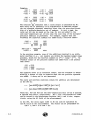
Figure 5-1 shows the formats for the classes and types of microcommands
executed by the CPU. The format for the logical and arithnetic classes
is identical. The general characteristics of each class and type are
defined below.
5 ~·.2 .• 1
Logical and Arithmetic Classes
·As· the name implies, the logical and arithmetic classes of microcommands ;
perform logical and arithmetic functions of one or two variables, as
specified 'hYi
.. the microconunand. The specific logical or arithmetic ·
:..
·•,\,
-~ c21s1adoa.:..xo
LOGICAL AND ARITHMETIC CLASSES
Branch Type
47
42 41
01
11
SB
I
37 36
I
OP
-'-.. -32
29
24 23
DN
I I
NX
AO
DN
NX
AO
I
20 19
MC
I
MX
16 15
12 11
I
I
BO
00
BF
Skip Type
SB
OP
MC
MX
LL
SPECIAL CLASS
Branch Type
01
OP
DN
I I
AO
MC
MX
so
OP
DN
I I
AO
MC
MX
so
SB
NX
BF
Skip Type
l_S SB
SB
= branch
NX
J-
FN
condition code (bit 47 specifies microconunand type)
OP = basic operation performed by the microcommand
DN
= destination
NX
= special
t
address of result from the arithmetic/logic unit (AU)
control functions
AO = source address of A operand to AU..
MC = microcondition code specification (dispositions)
MX
= special
control functions
BO = source address of B operand to AU
. SO =
spec~al
operation control functions
BF = branch.address or auxiliary control functions
LL
=
FN
= auxiliary
literal· value
control functions
Microcommand Fonnats
·c,21s10000;.:~o
I
operation i.s deJ!ined by. the OJ? field. A total of 16 l.ogj.cal and e.ight
a:ritlunetic opera,ti.ons a,:r:e i~le.IQented. The same set of· operations is
performed ~egardless of whether a branch- or skip-type microcommand is
used.
The logical or arithmetic branch-type microconunand permits the programmer to specify that a conditional or unconditional branch to a new program location can occur based on the results of executing the current
microcommand (or on results previously stored).
In this type of microconnnand, both an A and B operand to AU are specified.
The destination of the resulti_ng operation is also specified. Arithmetic
condition codes resulting from the microcommand execution can be saved or
ignored.
If a branch condition is specified, an 11-bit branch address is provided
that alters the microprogram sequence if the branch condition is met. A
control bit is also provided that can cause the next CM address to be
pushed into CS before the branch is made. This permits the microprogram
to later execute an automatic return to the microprogram.sequence via CS.
It is not necessary to specify a branch condition, even though the microcommand is a branch type. If no branch condition is specified, an auxiliary set of control functions can be specified that are performed
simultaneously with execution of the basic logical or arithmetic operation.
The remaining fields.of the branch-type microconnnand provide special
control functions that can modify execution and content of the next
microcommand in sequence. The operations performed by these fields are
common to all microcommands, regardless of class and type.
Skip-Type
The logical or arithmetic skip-type microconnnand performs the same basic
operations as the branch type. The differences in the skip-type microconunands are:
a. Instead of a branch condition, a condition is specified under
which exe·ctttion of the microconnnand at .the next CM location can
be inhibited (skipped). The CM address sequence itself is not
altered.
b. The B-operand source and branch address are replaced by a 16bi t literal value. This value is used directly as the B
operand for those logical and arithmetic operations that involve a B-operand input to AU.
c. Because of the space reserved for· a literal value (whether .or
not one is required) , the auxiliary control functions defin'ed
for the branch-type microconnnand cannot be specified.
All other operations of a skip-type microcommand are identical to the
branch-type microconnnand.
·corresp6n~ing
C2151B008-XO
s-3
5.2.2
Special Class
The special class of mi.crocommands provides . functions that af feet specialized control and other operations required of the computer. Some 0£
these microconunands involve the use of AU. The operation performed is
specified by the OP field. A total of seven special operations are implemented.
Branch-Type
The special branch-type microcommand permits the progrannner to specify a
conditional or unconditional branch just as for the logical or arithmetic branch type. And, in the same way, either a branch address or a
set of auxiliary control functions can be specified, depending on whether
or not a branch condition is specified by the microconnnand.
Skip-Type
The special skip-type microcommand is the same as the branch type and
specifies the same operations, except that:
a. Instead of a branch condition, a condition is specified under
which execution of the microcommand at the next CM location can
be inhibited (skipped). The CM address sequence itself is not
altered.
b. Since a branch address cannot be specified by this type of microcommand and since a B operand is never used, the space reserved
for these is used to specify a set of auxiliary control functions.
5.3
LOGICAL MICROCOMMANDS
The following paragraphs present a description of each logical microcommand. A summary of all the basic microconnnands executed by the CPU is
given in Table 5-1.
The description of each
OP-field code; symbolic
cable; a description of
comments to clarify the
5-4
microcommand includes the nmemonic; hexadecimal
notation describing its operation, where applithe function performed; and examples or other
description.
C21518008-x;O ·.
T~le
5-1.
Mnemonic
Cal Data 100 Engine Microcormnand Sunmlary
OP Field
(Hexadecimal)
Name
LOGICAL
EML
SXA
MVA
MVB
OCA
OCB
AND
NOB
NOA
NOR
ORI
ORB
ORA
NANO
XOR
COI
00
01
02
03
04
05
06
07
08
09
OA
OB
oc
OD
OE
OF
Emulate (optional)
Sign Extend A
Move A
Move B
Complement A
Complement B
AND A, B
AND A, B'
AND Jr, B
Not OR
OR A, B
OR A, B'
OR Jr, B
Not AND
Exclusive OR
Coincidence
ARITHMETIC
ADD
SUB
ADC
SBC
INC
DEC
MSA
-
10
11
12
13
14
15
16
17
Add, A, B
Subtract A, B
Add carry
Subtract carry
Increase ·A·
Decrease A
Add A Masked
(reserved)
..
SPECIAL
SHF
MUS
DVS
TSB
lA
CMA
lB
lC
lD
CMB
DCD
lF
MMS
cns1aooa~xo
18
19
lE
Shift
Multiply Step
Divide Step
Test Bit
Modify Macrostatus (optional)
Conditional Memory Access, A operand (.optional)
Conditional Memory Access, B operand
Decode (optional)
5-5·
The following symbols are used (in addition to many defined in Table
1-1):
11 = absolute value of
( ) = contents
( ) = Boolean
of
complement
n = Boolean
AND
U = Boolean OR
E9
= Boolean exclusive OR
=
= equal
<
= less than
>
= greater than or equal to
-:/
= not equal to
to
+ = arithmetic addition (two's complement)
= arithmetic subtraction (two's
x
= .arithmetic mul tiplicatio.n
.
= arithmetic division
complemen~)
A = A operand to AU (from A-operand source specified by the
microcommand)
An
= nth
.Aa:An •
A
bit of A
bit.· m to n
B
= B operand
R
= result
RM
to AU (from B-operand source specified by the
microcommand)
(word on MB)
= more-significant
byte of R
RL · = less-signficant byte of R
DN
= destination location (specified by the microcommand)
CIN
=
~
= replaces
carry input
The logical microcommands listed in Table 5-1 can be e~ecuted in either
the word or byte mode. With one exception (SXA) ,; :·~~{_;'operation is performed on the full pair of operand words in Au· atjd_.::.t?fe·. 16-bit result is
transferred to the destination via MB.
·S-6
.·.c;:21s1aooa-xo
Microcondition codes are determined on the full word in the word mode
and on the less-significant byte in the byte mode. This is illustrated
below:
AU
AU
00
15
R
\
00
08 07
15
RM
)
RL
'--.,-----I
""
Microcondition
Microcondition
Code Test
Code Test
The microcondition codes for all logical-class microcommands are given
in Table 5-2.
All logical microcommands are standard except Emulate (EML), which is
optional. The main purpose of EML is for very rapid emulation decoding
of instruction operation codes and control fi~lds. The procedure is
to store the instruction in IR. EML then initiates translation of the
contents of IR into a CM branch address generated from a table of values.
The address directs the microprogram to the proper microroutine in CM
for-the emulation of each instruction. The emulate table is specifically programmed for each computer to be emulated. The decoding operation performed by EML can be accomplished by other methods using only
standard microcommands, but at the cost of time and CM space. For this
reason, the need to implement EML depends on the specific application.
Table 5-2.
Microcondition Codes for Logical Microcommands.
Microcondition
Code
c
v
z
n
p
d
C21518008~XO
Definition
Word Mode
Byte Mode
~~ontrolled
~~ontrolled
by the MC
field of the microcommand
1 if R=O; 0 otherwise
1 if Rl5=1; 0 otherwise
1 if" R>O; 0 otherwise
1 if ROO=l; 0 otherwise
by the MC
field of the microcommand
1 if RL=O; 0 other~ise
1 if R07=1; 0 otheiw~~e
1 if RL>O; o otherwis~
1 if ROO=l; 0 otherwis'e
5-7;
5.3.l
Emulate (Optional)
Mnemonic:
EML $00
Operation:
R= A
R +{DN)
(emulation table)+{CC), unless higher-priority CC
modification occurs
Description:
5.3.2
·The A operand is transferred to the destination. The
contents of IR are translated into a branch address
(emulate instruction address, EIA) to CC using an
emulate table on the ~ulate Board. If a higherpriori ty CC modification occurs concurrent with the
microcommand, the EIA is ignored. All microcommand
fields are effective as def~ned, except that the BO
field is ignored, since no B operand is used.
Sign Extend A
Mnemonic:
Operation:
SXA $01
Word mode
Byte mode
RM =(N)U Al5:A08
RL = A07 :AOO
RM, RL+{DN)
R=A
. R +(DN)
Description:
In the word mode, the A operand is transferred to the
destination.
In the byte mode, the state of the negative microstatus
bit, N, is extended to the more-significant byte of the
A operand. The contents of the less-significant byte
of the A operand are unmodified. The result is transferred to the destination.
Example:
Perform a byte mode add on A and B and store the result
in. the A-operand location, then extend the sign of the
byte result.
A
+B
R
00000000 10110100
00000000 11101100
00000001 10100000
(-76)
(-20)
(-96)
The microcondition codes generated are:
1 =·1, v = O, z = O, n = 11 p = O, d = O
SXA:
· A
U(N)
R
00000001 10100000
11111111
11111111 10100000
~
RM
5-8
'--..,,----/
RL
C215iB008-XO
5.3.3
Move A
Mnemonic:
Operation:
MVA $02
R
=
A
R -~ (DN)
Description:
5.3.4
The A operand is transferred unmodified to the
destination.
Move B
Mnemonic:
MVB $03
Operation:
R
=
B
R - - . (DN)
Description:
5.3.5
1
The B operand is transferred unmodified to the
destination.
Complement A
Mnemonic:
Operation:
OCA
R
=
$04
A
R ~(DN)
Description:
The logical or one's complement of the A operand is
transferred to the destination.
Example:
A
R
5.3.6
Binary
0110110100101100
1001001011010011
Octal
Hexadecimal
066454
6D2C
111323
9203
Complement B
Mnemonic:
OCB $05
Operation:
R
Description:
The logical or one's complement of the B operand
is transferred to the destination •.
C21518008'."'"XO
= B"
R -.(DN)
5-9
5.3.7
AND A, B
Mnemonic:
Operation:
AND $06
R
=
An B
R - - . (DN)
Description:
5.3.8
AND
The logical AND of the A and B operands is transferred to
the destination.
A, B'
Mnemonic:
NDB $07
Operation:
Description:
5.3.9
5.3.10
AND A, B
Mnemonic:
NDA $08
Operation:
R = An B
R --.. (DN)
Description:
The logical complement of the A operand. is ANDed
with the B operand and the resµlt is transferred
to the destination.
Not OR
Mnemonic:
NOR $09
Operation:
R
R
Description:
s-io
The logical comptement of the B operand is ANDed with
the A operand and the result is transferred to the
destination.
=
~
AU B
(DN)
The logical NOR of the A and B operands is transferred
to the destination.
c21s1aooa-x6
5.3.11
OR A, B
Mnemonic:
ORI $0A
Operation:
R
R
Description:
5.3.12
5.3.14
The logical OR of the A and B operands is transferred
to the destination.
OR A, B
Mnemonic:
ORB $OB
Operation:
R
R
Description:
5.3.13
AU B
=
~(DN)
=
~
A U B"
(DN)
The logical complement of the B operand is ORed with the
A operand and the result is transferred to the destination.
OR A, B
Mnemonic:
ORA $0C
Operation:
R = Jr U B
R __.. (DN)
Description:
The logical complement of the A operand is ORed with
the B operand and the result is transferred to the
destination.
Not AND
Mnemonic:
NAND
Operation:
R
R
Description:
C21518008-}{0
$00
=
~
An B
(DN)
The logical NANO of the A and B operands is transferred
to the destination.
5-11
5.3.15
Exclusive OR
Mnemonic:
Operation:
XOR
R·=A
$OE
(!) B
R _ . (DN)
Description:
The logical exclusive OR of the A and B operands is
transferred to the destination. The exclusive OR by
definition is:
A(f) B= [A nBJ u [x nB]
5.3.16
Coincidence
Mnemonic:
Operation:
Description:
COT
$OF
R=A eR
R __,. (Dm
The complement of the logical exclusive OR of the A and
B operands is transferred to the destination. This is
the coincidence function:
A (f) B= [An B] u (An BJ
5.4
ARITHMETIC MICROCOMMANDS
The arithmetic microcommands are 1 i.sted ir: TabL=- 5-1.
microcomma~ds in this class.
't'l: ::! ..... e are eight
The CPU performs both binary addition and subtraction (as opposed to
complementary addition). Negative numbers are. assumed to be represented
as two's complements of positive numbers (although one's complement
arithmetic can be performed, since the progrannner has independent control of the carry and borrow inputs to AU). A complete description of
binary arithmetic operations in the CPU is given in Appendix A. The
carry and overflow microcondition codes differ for the addition and
subtraction operations, as does the us(~ of the rarry-in t?nn. The data
value microcondition codes (z, n, p and d) are the same for addition and
subtraction and depend, only on the value.of the arithmetic result.
Arithmetic.operations .can be executed in either the word or byte mode.
In either mode, .th~.· specified operation is performed on the full pair of
operand words in At.L: .·.The 16-bit result is transferred to the destination via MB. The midrocondi tion codes are de.termined on the full word
in the word mode ari~··,on. t}?-e less-significant byte in the byte mode (see
illustration in sulis:ectiori 5 •. :i) • The microcondi tion codes for addition
and subtraction operations are defined in.Table 5-3.
Table 5-3.
Micro
Condition
Code
c
v
Microcondition Codes for Arithmetic Microcammands
Arithmetic
Opena.tion
n
n
p
d
. ~1518008,-XO
J u [ Bl5 nRl.5 J
Addition
[AlS Rl.5
U (AlS Bl5]
Subtraction
[AlS R15] [A15
U(Bl5 R15]
n
n
n
u
n
u
[A07 R07] [B07
U(A07 B07] ·
nBl5]
[ A07
n
nR07 J
nR17] ~A07 nB07]
u(ao1
na15 nRls]
n [A1s nsis nns]
[ AlS nBlS nRl.tl_
U(Al5 nBl5 nRlS]
Addition
nRo7
~A07 nB07 n RD7]
[Als
Subtraction
z
Definition
Byte Mode
Word Mode
[Ao7 nB0'7 nRo1 J
n
n
(Ao7 Bo1 RozL
[A07 B07 R07]
u
n
= 0;
Addition or
1
Subtraction
0 otherwise
0 otherwise
Addition or
1 if RlS = 1;
1 if R07 =. l;
Subtraction
O otherwise
0 otherwise
Addition or
1 if R > 0;
1 if RL > 0;
Subtraction
0 otherwise
0 otherwise
Addition or
1 if ROO = l;
Subtraction
0 otherwise
if R = O;
1 if RL
...
n
1 if ROO = l;
0 otherwise
5'-13
5.4.1
Add A, B
Mnemonic:
Operation:
ADD $10
R=A+B+cIN
(DN)
R __....
Description:
The A and B operands and the value of CIN designated by
the MC field are added arithmetically and the result is
transferred to the destination.
Microcondi tion
Codes:
Addition (Table 5-3).
Example:
Add A and B and
A= +27,435
+B = - 1,747
+CIN =
+l
R = +25,689
increment the result:
= 0110101100101011
= 1111100100101101
= 0000000000000001
=l 0110010001011001
l
.. c
The microcondition codes generated are:
c = 1, v = O, z = O, n = O, p = 1, d = 1
5.4.2
Subtract A, B
Mnemonic:
SUB $11
Operation:
R=A-B-CIN
R __.(ON)
Description:
The B operand and the value of CIN designated by the
MC field are subtracted from the A operand and the
.result is transferred to the destination.
Microcondition
Codes:
Subtraction (Table 5-3).
Example:
Subtract B from A
A·=
-444
-B = -(-1,747)
-CIN
-(+l)
R = ' . +l, 392
=
and decrement the result:
=
1111111001000100
=
- 1111100100101101
= - 0000000000000001
=
0 0000010100010110
Le
This operation produces a one's complement result when
the result is negative, since CIN is specified as a ONE.
The microcondition codes generated are:
c = O, v = O, z = O, n = 0, p = 1, d = O
5....:14
c2°1518008-XO
5.4.3
Add Carry
Mnemonic:
Operation:
ADC $12
R=A+cIN
R --.(ON)
Description:
The value of CIN designated by the MC field is added
to the A operand and the result is transferred to the
destination.
Microcondi tion
Codes:
Addition (Table 5-3).
5.4.4 Subtract Carry
Mnemonic:
Operation:
SBC $13
R=A-CIN
R __.(ON)
Destination:
The value of CIN designated by the MC field is subtracted
from the A operand and the result is transferred to the
destination.
Microcondi tion
Codes:
Subtraction (Table 5-3).
C215180.Q8.~'XO
s:-rs
5.4.5
Increase A
Mnemonic:
INC $14
Ope:r;:ation:
R=A+l+cIN
R ---.(DN)
Description:
The value one and the value of CIN des_ignated ·by the
MC field are added to the A operand and the result is
transferred to the destination. If CIN is ONE, the
A operand is increased by two; otherwise, it is
increased by one.
Microcondi tion
Codes:
Addition (Table 5-3),
Examples:
Increase the A operand by two if MC designates CIN as
ONE; increase by one otherwise:
A = +7817 = 0001111010001001
+l =
+l = 0000000000000001
+CIN =
0 = 0000000000000000
R = +7818 = 0001111010001010
The microcondition codes generated are:
c = O, v = 0, z = O, n = 0, p = l, d = 0
Another example, where overflow is affected:
A= +32,766 = 0111111111111110
+l =
+l = 0000000000000001
+l = 0000000000000001
+CIN·=
R = +32,768 = 1000000000000000
The microcondition codes generated are:
c = O, v = 1, z = O, n = 1, p = 0, d
5-16
=0
C215l.8008-XO
5.4.6
Decrease A
Mnemonic:
Operation:
DEC $15
R=A-1-CIN
R __. (DN)
Description:
The quantity one and the value of CIN designated by the
MC field are subtracted from the A operand and the
result is transferred to the destination. If CIN is ONE,
the A operand is decreased by two; otherwise, it is
decreased by one.
Microcondi tion
Codes:
Subtraction (Table 5-3).
Example:
Decrease the A operand by two if the L microstatus bit
is set; decrease by one otherwise:
a. If (L) = 1:
A=
+l =
0000000000000001
-1 = -(+l) = - 0000000000000001.
CIN = -(+l) = - 0000000000000001
R = -(+l) = 1 1111111111111111
l_.c
The microcondition codes generated are:
c = 1 (borrow), v = O, z = O, n = 1,
p =
h.
o,
d = 1
If (L)
A=
-1
= 0:
0000000000000001
0000000000000001
-0 = - 0000000000000000
0 =
0000000000000000
+l =
= -(+l) = -
CIN =
R =
The microcondition codes generated are:
C = 0 I V = 0 I Z = 1, n = 0 I p = (f~\·$i = Q
1
C21518008-XO
5-17,
5.4.7
Add A Masked
Mnemonic:
MSA $16
Operation:
R=A+ [A RB] +cIN
R __. (DN)
Description:
The logical AND of the A and B operands is added to
the A operand and to the value of CIN designated by
the MC field, and the result is transferred to the
destination.
Microcondi tion
Codes:
Addition (Table 5-3).
Example:
Add the absolute value of the less-significant byte of
A to the A operand:
A =
-110 = 1111111110010010
B = mask = 0000000001111111
An B =
+18 = 0000000000010010
+A =+(-110) = 1111111110010010
+CIN =
+O = 0000000000000000
R =
· -92 = 1111111110100100
The microcondition codes generated are:
c = O, v = O, z = O, n = 1, p = O, d
5~18
=0
'C21518008-XO
5.5
SPECIAL MICROCOMMANDS
The seven special microcommands listed in Table 5-1 provide a powerful
extension of the basic logical and arithmetic microcommands. Four of
these are standard and have general application in all emulation microprograms. Three microcommands are defined as optional, since they must
be tailored to a particular emulation system. The hardware elements
that implement the optional microconnnands are modularized to permit them
to be either omitted or redefined without affecting the basic hardware
of the Engine.
Microcondition codes generated for the special microconnnands are
generally identical to those defined for the arithmetic microconunands,
with major exceptions. The overall uses and limitations of the special
microcommands are described in the following paragraphs.
G.21s1aooa~xo
5-19.
5.5.1
Shift
The Shift microconnnand provides complete flexibility for single-length
shifts involving only the A operand and AU, and double-length shifts
involving AU and XR. Shifts can be left or right, logical or
arithmetic, open or closed. While the basic microconnnand shifts only
a single bit, multibit shifts can be performed by repeating the microcommand using LC.
Mnemonic:
SHF $18
Microconnnand
Special branch or special skip.
Type:
Description:
The SO field specifies the type and direction of shift
as shown in Table 5-4. For a single-precision (16-bit)
shift, the A operand is shifted one place left or right
and the result is transferred to the destination. For
a double-precision (32-bit) shift, the A operand and the
contents of XR are shifted one place left or right with
a linked carry between the two words. The shifted AU
result is transferred to the destination and the
shifted XR result remains in XR. The shift operation
is performed in the word mode unless a byte operation
is specified by the FN field.
Using the special skip-type format for the shift can
lead to possible conflict between a double-length shift
specification in the SO field ~d an XR shift specif ication in the FN field. If such.a conflicting specification is made, the SO field control is effective and the
FN field control is ignored.
Table 5-4.
SO-Field Shift Specification
so Field Bits
15
14
13
12
0
0
1
1
x
x
x
x
0
1
0
1
x
x
x
x
x
x
x
x
0
·1
x
x
x
x
x
x
x
x
0.
l\
Shift Operation
swap halves
shift left, logical
shift right, logical
shift right, arithmetic
single precision
double precision
open shift
closed shift
C1l518008-XO
5.5.1.1
Single-Precision Shifts.
Single-precision shifts involve only AU shift elements operating on
the A operand.
Swap Halves (Word or Byte).
Operation:
a.
Word mode :
Rl5 :R08=A07 :AOO
R07:ROO=Al5:A08
R
.. (DN)
15 14 13 12 11 10 09 08 07 06 05 04 03 02 01 00
AM
I
b.
~
AL
I
I
E
Byte mode:
Rl5: R08=Al5 :AOS
R07:R04=A03:AOO
R03 :ROO=A07 :A04
R·
.. (DN)
15 14 13 12 11 10 09 08 07 06 05 04 03 02 01 00
AM
;C21!)18008-XO
AL
5-21
Description:
For word swaps, the more-significant and less-significant
bytes of the A operand are swapped and the result is
transferred to the destination.
For byte swaps, the more-significant and less-significant
halves of the less-significant byte of the A operand are
swapped and the result is transferred to the lesssignif icant byte of the destination. The more-significant
byte of the A operand is transferred, unchanged, to the
more-significant byte of the destination.
Microcondition
Codes:
5....:22
a.
Word mode:
c = AlS
Al4
v = AlS
z = 1 if R=O;
0 otherwise
n = 1 if RlS=l;
0 otherwise
p = 1 if R>O;
0 otherwise
d = 1 if ROO=l;
0 otherwise
e
b.
Byte Mode:
c = A07
v= A07 <3' A06
z = 1 if RL=O
0 otherwise
n = 1 if R07=1;
0 otherwise
p = 1 if RL>O;
0 otherwise
d = 1 if ROO=l;
0 otherwise
·C21518008-:-XO
Logical 0pen Left Shift (Word or Byte).
Operation:
a.
Word mode :
c
b.
--i
15 14 13 12 11 10 09 08 07 06 05 04 03 02 01 00
A
Byte mode:
15 14 13 12 11 10 09 08
I
AM
r
I
07 06 05
0~03
1--
02 01 OOr- CIN
c ..
Description:
For word shifts, the A operand is shifted left one bit.
The value of CIN designated by the MC field is shifted
into bit 00. The bit shifted out of bit 15 is the shift
carry out. The result is transferred to the destination.
Byte shifts are the same as word shifts, except that the
shift is on the less-significant byte only. The carry
bit is shifted out of bit 07. The more-significant
byte is unmodified. The resulting word is transferred
to the destination.
Microcondition
Codes:
. C2!'51,8008-XO
a.
Word·Mode:
c = AlS
v = Al5 (!) Al4
z = 1 if R=O;
0 otherwise·
n = 1 if RlS=l;
0 otherwise
p = 1 if R>O;
0 otherwise
d = 1 if ROO=l;
0 otherwise
b.
CIN
Byte mode:
c = A07
v = A07 (!) A06
z = 1 if RL=O;
0 otherwise
n = 1 if R07=1;
0 otherwise
p = 1 if RL>O;
0 otherwise
d = 1 if ROO=l;
0 otherwise
·5-23
Logical Closed Left Shift (Word or Byte).
Operation:
a.
Word mode :
15 14 13 12 11 10 09 08 07 06 05 04 03 02
c
b.
..
00~
Byte mode:
i1.__5_.__1_4_.__1_3..._l_~
....1-1--l-0_.__0_9...._0_8,
c ..
Description:
01
A
n
07 06 OS 0::3 02 01 00 .,.
1
L
For word shifts, the A operand is shifted left one
bit. Bit 15 is the shift carry out and is also
shifted into bit 00. The result is transferred to
the destination. ·
Byte shifts are the same as word shifts, except that
the shift is on the less-significant byte only. The
carry bit is shifted out of bit 07. The moresignificant byte is unmodified. The resulting word
is transferred to the destination.
Microcondition
Codes:
a.
Word mode:
c.= AlS
v = Al5 E0 Al4
z = 1 if R=O;
O otherwise
n = 1 if RlS=l;
0 otherwise
p = 1 if R>O;
0 otherwise
d= 1 if ROO=l;
0 otherwise
b.
Byte mode:
c = A07
v = A07 (T) A06
z = 1 if RL=O;
0 otherwise
n = 1 if R07=1;
0 otherwise
p = 1 if RL>O;
0 otherwise
d = 1 if ROO=l;
0 otherwise
C215180QSO::XQ
Logical Open Right Shift (Word or Byte).
Operation:
a.
Word mode:
crn----j
b.
15 14 13 12 11 10 09 08 07 06 05 04 03 02 01 00
~c
Byte mode:
115 14 13
Description:
A
1~11
10 09 _0_8_1_~ 07 06 05
o:i,oJ
02 01
oar c
CIN
·
For word shifts, the A operand is shifted one bit to
the right. The value of CIN designated by the MC
field is shifted into bit 15. The bit shifted out
of bit 00 is the shift carry out. The result is
transferred to the destination.
Byte shifts are,the same as word shifts, except that
the shift is on the less-significant byte only. The
value of CIN is shifted into bit 07. The moresignificant byte is unmodified. The resulting word
is transferred to the destination.
Microcondition
Codes:
C21518008,;_XO
a.
Word mode:
c = AOO
v= Al5 <!) CIN
z = 1 if R=O;
0 otherwise
n = 1 if RlS=l;
0 otherwise
p = 1 if R>O;
0 otherwise
d = 1 if ROO=l;
0 otherwise
'•
b.
Byte mode:
c = AOO
v= A07 (!) CIN
z = 1 if RL=O;
0 otherwise
n= 1 if R07=1;
0 otherwise
p = 1 if RL>O;
0 otherwise
d = 1 if ROO=l;
O otherwise
S.;..'25
Logical Closed Right Shift (Word or Byte) :
Operation:
a.
Word mode:
15 14 13 12 11 10 09 08 07 06 05 04 03 02 01 00
d
b.
A
Description:
AM
I
r07 06 05 0:;3 02 01 00
... c
1
1
1
1
1
I
For word shifts, the A operand is shifted right one
bit. Bit 00 is the shift carry out and is also
shifted into bit 15. The result is transferred to
the destination.
Byte shifts are the same as word shifts, except that
the shift is on the less-significant byte only. The
carry bit is shifted into bit 07. The more-significant
byte is unmodified. The resulting word is transferred
to the destination.
Microcondition
Codes:
'5-26
a.
.. c
Byte mode:
15 14 13 12 11 10 09 08
I
IJ
Word mode:
c = AOO
v - Al5 e AOO
z = l if R=O;
0 otherwise
n = 1 if RlS=l;
0 otherwise
p = 1 if R>O;
0 otherwise
d = 1 if ROO=l;
0 otherwise
'•
b.
Byte mode:
c = AOO
v= A07
AOO
z = 1 if RL=O;
0 otherwise
n = 1 if R07=1;
0 otherwise
p = l if RL>O;
0 otherwise
d = l if ROO=l;
0 otherwise
e
C21518.008..;. xcf.
Arithmetic Open Right Shift (Word or Byte)_:
Operation:
a. Word mode:
15 14 13 12 11 10 09 08 07 06 05 04 03 02 01 00
CIN
(N)
~'
.....
b.
·--·---
A
:---
I-
Byte mode:
15 14 13 12 11 10 09 08
r---1
--AM-~IN__,df
AL
07 06 05 04 03 02 01 00
~c
(N)------'
Description:
For word shifts, the A operand is shifted right one
bit. The state of the N microstatus bit, ORed
with the value of CIN designated by the MC field,
is shifted into bit 15. Bit 00 is the shift carry out.
The result is transferred to the destination.
Byte shifts are the same as word shifts, except that the
shift is on the less-significant byte only. The value
of N ORed with CIN is shifted into bit 07. The moresignificant byte is unmodified. The resulting word
is transferred to the destination.
Microcondition
Codes:
ci~st0000-xo
a.
c
Word mode:
c = AOO
AlS (£) CIN U (N)
v
z = 1 if R=O;
0 otherwise
n = 1 if RlS=l;
0 otherwise
p
1 if R>O;
0 otherwise
d= 1 i f ROO =1;
O otherwise
b.
Byte mode:
c = AOO
v = A07 (!) CIN LJ (N)
z = 1 if RL=O;
0 otherwise
n = 1 if R07=1;
0 otherwise
p = 1 if RL>O;
0 otherwise
d = 1 if ROO=l;
0 otherwise
5-27
Arithmetic Closed Right Shift (Word or Byte).
Description:
Same as logical closed right shift.
5.5.1.2 Double-Precision Shifts.
Double-precision shifts involve AU shift elements and XR. When a
double-precision shift is specified in the SO field, an XR shift
operation specified by the FN field is ignored.
Swap Halves (Word or Byte).
Description:
s-ia.
Operation on the A operand and the microcondition codes
generated are the same as for single-precision swap.
The contents of XR are unmodified.
· c21s1aooa;..xo
Logical 0pen Left Shift (Word or Byte).
Operation:
a.
Word mode:
15 14 13 12 11 10 09 08 07 06 05 04·03 02 01 00
A
15 14 13 12 11 10 09 08 07 06 05 04 03 02 01 00
XR
b.
CIN
Byte mode:
15 14 13 12 11 10 09 08
I
AM
07 06 05 04 03 02 01 00
I
AL
c
15 14 13 12 11 10 09 08 07 06 05 04 03 02 01 00
CIN
XR
Description:
For word shifts, the A oper~nd and the contents·of XR
ar~ shifted left one bit.
The value of CIN designated
by the MC field is shifted into XR bit 00. The XR
bit 15 is shifted into the A-operand bit 00. A-operand
bit 15 is the shift carry out. The shifted A-operand
result is transferred to the destination. The shifted
XR result remains in XR.
Byte shifts are the same as word shifts, except that
the A-operand shift is on the less-significant byte
only. A-operand bit 07 is the shift carry out. The
more-significant byte is unmodified.
Microcondition
Codes:
C21518.Q08..;.xo· · ·
a.
Word modes:
c = AlS
v= Al5 (!) Al4
z = 1 if A=O;
0 otherwise
n = 1 if AlS=l;
0 otherwise
p = 1 if A>O;
O otherwise
d = 1 if XRlS=l;
0 otherwise
b.
Byte modes:
c = A07
v = A07 (!) A06
z = 1 if AL=O;
0
n = 1
0
p .=:= 1
otherwise
if A07=1;
otherwise
if AL>O;
0 otherwise
d; 1 if XR15=1;
O otherwise
•{
. . 5:--29 -
Logical Closed Left Shift (Word or Byte).
Operation:
a.
Word mode:
15 14 13 12 11 10 09 08 07 06 05 04 03 02 01 00
A
15 14 13 12 11 10 09 08 07 06 OS 04 03 02 01 00
XR
b.
Byte mode:
15 14 13 12 11 10 09 08
I
AM
07 06 05 04 03 02 01 00
I
AL
c-----~~~~~~~~~~~~__.
15 14 13 12 11 10 09 08 07 06 05 04 03 02 01 00
XR
Description:
For word shifts, the A operand and the contents of XR
are shifted left one bit. XR bit 15 is shifted into
A-operand bit 00. A-operand bit 15 is the shift carry
out and is also shifted into XR bit 00. The shifted
A-operand result is transfe~red to the destination.
The shifted XR result remains in XR.
Byte shifts are the same as word shifts, except that
the A-operand shift is on the less-significant byte
only. A-operand bit 07 is the shift carry-out and
is also shifted into XR bit 00. The more-significant
byte is unmodified.
Microcondi tion
Codes:
. .'
~.~30
Same as logical open left shift.
C215~8008-XO
Logical Open Right Shift (Word or Byte).
Operation:
a.
Word mode:
15 14 13 12 11 10 09 08 07 06 OS 04 03 02 01 00
CIN
XR
lS 14 13 12 11 10 09 08 07 06 OS 04 03 02 01 00
c
A
b.
Byte mode:
lS 14 13 12 11 10 09 08 07 06 OS 04 03 02 01 00
Xlt
CIN
lS 14 13 12 11 10 09 08
I
Description:
AM
I
07 06.0S 04 03 02 01 00
AL
For word shifts, the A operand and the contents of XR
are shifted right one bit. The state of CIN designated
by the MC field is shifted into XR bit lS. XR bit 00
is shifted into A-operand bi~ lS. A-operand bit 00
is the shift carry out. The ·shifted A-operand result is
transferred to the destination. The shifted XR result
remains in XR.
Byte shifts are the same as word shifts, except that the
A-operand shift is on the less-significant byte only.
XR bit 00 is shifted into A-operand bit 07. The moresignificant byte is unmodified.
Microcondi tion
Codes:
C21518008-.XO
a.
Word mode:
c = AOO
v= XROO ~ AlS
z = 1 if A=O;
0 otherwise
n = 1 if XRlS=l;
0 otherwise
p = 1 if A>O;
= 0 otherwise
d = 1 if AOO=l;
0 otherwise
b.
Byte mode:
c = AOO
v = XROO (!) A07
z = 1 if AL=O;
0 otherwise
n= 1 if XRlS=l;
0 otherwise
p ;:: 1 if AL>O;
0 otherwise
d·= 1 if AOO=l;
:0 otherwise
c
Logical Closed Right Shift (Word or Byte).
Operation:
a.
Word mode:
15 14 13 12 11 10 09 08 07 06 05 04 03 02 01 00
XR
15 14 13 12 11 10 09 08 07 06 05 04 03 02 01 00
A
b.
Byte mode:
15 14 13 12 11 10 09 08 07 06 05 04 03 02 01 00
XR
15 14 13 12 11 10 09 08
I
Description:
AM
I
07 06 05 04 03 02 01 00
AL
For word shifts, the A operand and the contents of XR
are shifted right one bit. XR bit 00 is shifted into
A-operand bit 15. A-operand bit 00 is the shift carry
out. The shifted A-operand is transferred to the . ,
destination. The shifted XR result remains in XR.
Byte shifts are the same as word shifts, except that
the A-operand shift is on the less-significant byte
only. XR bit 00 is shifted into A-operand bit 07.
The more-significant byte is unmodified.
Microcondi tion
Codes:
·s~32 .
Same as logical open right shift.
c21si0oos-xo
Arithmetic 0pen Right Shift (Word or Byte).
Operation:
a. Word mode:
15 14 13 12 11 10 09 08 07 06 05 04 03 02 01 00
CIN
XR
15 14 13 12 11 10 09 08 07 06 05 04 03 02 01 00
c
A
b.
Byte mode:
15 14 13 12 11 10 09 08 07 06 05 04 03 02 01 00
XR
CIN
15
I
Description:
l~
13 12 11 10 09 08
AM
I
07 06 05 04 03 02 01 00
c
AL
For word shifts, the A operand and the contents of XR
are shifted right one bit. XR bit 15, ORed with the
state of CIN designated by the MC field, is shifted
into XR bit 15. XR bit 00 is shifted into A-operand
bit 15. A-operand result is transferred to the destination. The shifted XR result remains in XR.
Byte shifts are the same as word shifts, except that
the A-operand shift is on the less-significant byte
only. XR bit 00 is shifted into A-operand bit 07.
The more-significant byte is unmodified.
Microcondi tion
Codes:
Same as logical open right shift.
_Arithmetic Closed Right Shift (Word or Byte).
Description:
.c21510000:..:.:xo
Same as logical closed right shift.
5'.'""33
5.5.2
Multiply Step
The MUS microcommand is a specialized version of the Shift microconunand
with an automatic iterative repeat that permits high-speed implementation of a Multiply instruction. The average execution time is 300 ns
per bit plus the additional time required to preformat the multiplier
and multiplicand, determine the sign of the product and fonnat the final
result. No additional hardware is required for the high-speed multiply
function, since all operations are implemented in control memory.
Mnemonic:
MUS
Microconunand
Special branch
$19
Type:
Description:
The MUS microcomffiand provides a set of simultaneous add,
shift and test operations involving a register containing
the multiplier (MPR) plus XR, LC and the state of the
next MPR digit. The microconunand is automatically repeated until (LC)=O. For each ONE in MPR, a branch is
made to a microcommand that adds the multiplicand (MPD)
to XR. This permits complete execution of multiply steps
in one clock cycle for a ZEEO MPR digit and three clock
cycles for a ONE MPR digit. The MUS microcommand is used
for multiplication of two 16-bit operands with a resulting
32-bit product.
Registers
Used:
a.
b.
c.
d.
e.
SO Field:
5-34
MPR in a register designated by the AO field of the
MUS microconunand. This register contains the moresignificant half of the product at the end of the
complete multiplication.
MCD in a register designated by a separate microcommand that adds MCD to the partial product.
XR, which accumulates MCD additions to the partial
product and contains the less-significant half of the
product at the end of the complete multiplication.
LC, which counts the number of MUS iterations performed.
The L microstatus bit, used to propagate carries from
the less-significant half to the more-significant
half of the partial product.
The SO field must be progrannned for a double-precision,
logical open lift shift (bits 15:12 = $6), as specified.
in the Shift microcommand description (Table 5-4).
C21518008-XO
Operation:
The following operations are executed simultaneously
by the MUS microcommand.
Entry
Shift left(XR);
XR carry to
shift gates
Add MPR+ (L) ;
shift sum left;
add XR carry
(LC)-l+(LC);
reset L
G2.:L5180Q8-XO
5-35
Procedure:
1.
Convert MCD to a positive number:
15 14 13 12 11 10 09 08 07 06 05 04 03 02 01 00
lol
2.
Convert MPR to a positive number, shift left and
test MPR relative to zero:
15 14 13 12 11 10 09 08 07 06 05 04 03 02 01 00
•
3.
4.
I
~0
I
lol
MPR
Initial conditions:
(XR)=O
(L) =O
(LC)=lS (for a 16-bit multiplication)
Program MUS control fields as follows:
SB = $10 (dynamic branch < 0)
OP = $19 (MUS)
DN = MPR address
NX = $3 (inhibit next microconnnand, if branch)
AO = MPR address
MC = $6 (add and update L)
MX = $0 (no operation)
so = $6 (double-precision logical open left shift)
BF = MUS location minus one
The symbolic microassembler automatically sets up
all fields except DN and AO.
5.
5-36
For the final double-length result, the MPR register
and XR must be shifted right one bit after the last
iteration. This can be performed using the standard
SHF microconnnand programmed for a double-precision
logical open right shift. The sign of the product
must also be determined and inserted.
c2 r51aooa:..·xo
6.
The basic microconnnand sequence is illustrated
below:
Entry
Execute
MUS
No
MCD+(XR)
+(XR);
c+(L)
Yes
Shift MPR
and (XR)
right
Determine
and insert
sign
Yes
Repeat MUS
· . ,C2.15180p8-XO
5-37
MicroCondi tion
Codes:
Example:
c
v
z
n
=
=
=
=
AU shift carry
shift overflow
1 if AU shift result
1 if AU shift result
0 otherwise
p = 1 if AU shift result
d = 1 if AU shift result
0 otherwise
=O; O otherwise
most-significant bit
=
O;
> O; O otherwise
least-significant bit = O;
Multiply the following four-bit numbers (all registers
assumed to be four bits) :
MPR = 0101
MCD = 0111
MPR
L
XR
LC
Explanation
3
Initial condition
Shift MPR left; test MPR<O
Add MCD to ( XR)
Add (L) to MPR
2
Shift MPR and (XR) left
1
Add MCD to (XR)
0
0100
\ 0010
0110
0011./
Exit, (LC)=O
Shift MPR and (XR) right for final
product~·:
product
.: :-5-38
-'c21s1aooa~x_o
5.5.3
Divide Step
The DVS microcommand is a specialized version of the subtract operation
(conditional} with an automatic iterative repeat that permits highspeed implementation of a Divide instruction. The fixed execution time
is two clock cycles per bit plus the time required to preformat the
divisor and dividend, check for overflow, determine the sign .of the
quotient and format the final result. No additional hardware is required
for the high-speed division, since all operations are implemented in
control me100ry.
Mnemonic:
DVS
Microcommand
Special branch.
$1A
Type:
Operation:
R= A + B + 1
If c=l, R+A
Description:
The DVS microcommand executes a two's complement addition
of the divisor (DVR} to the more-significant word of a
double-precision dividend (DVD}. If a carry out is
generated by the addition, the result replaces the moresignificant word of DVD; otherwise DVD is unchanged.
The carry out must be saved in the L microstatus bit.
the microcommand is used in conjunction with a doublelength left shift of the A operand and XR on each
iteration, with the carry out saved in L shifted into XR.
DVS can be automatically repeated using LC. The result
is a single-length quotient with a single-length remainder.
Registers
Used:
a.
b.
c.
d.
e.
Procedure:
1.
DVD more-significant word (DVDM} in a file register
designated by the AO field of the DVS microcommand.
This register contains the remainder at the end of
the complete division operation.
DVD less-significant word (DVDL} in XR.
DVR in a register designated by the BO field of the
DVS microcommand. This register contains the
quotient at the end of the complete division
operation.
LC, which counts the number of iterations performed.
The L microstatus bit used to propagate quotient
bits into XR.
Convert DVD to a 31-bit positive number:
15 14 13 12 11 10 09 08. 07 06 05 04 03 02 01 00
K.
XR
D~~.
I
;::,
15 14 13 12 i1.10 09 08 01 06 .o5 o4
oi oi
01 oo
DVDL
A Operand
d1518bo'8~xo···
5-39·
2.
Convert DVR to a positive number:
15 14 13 12 11 10 09 08 07 06 05 04 03 02 01 00
joj
I
DVR
B operand
3.
4.
5.
6.
7.
. 5-:-40
Test for DVR <2 X DVD. If true, set overflow
and exit.
If no overflow, shift DVD left and set initial
conditions:
(L)=O
(LC)=l5
Program DVS control fields as follows:
SB = $03 (branch if (LC)=O before decrementing)
OP = $1A (DVS)
DN = DVDL
NX = $1 (execute next microcommand, if branch)
AO = DVDM
MC = $5 (modify link status; CIN=l)
MX = $0 (no operation)
BO = DVR
BF = location of DVS
The symbolic microassembler automatically sets
up all fields except DN, AO and BO.
DVS is used in conjunction with a double-length
left shift on the A operand and XR, with L added
to XR.
The final double-length result must be left
shifted one bit after the f~al iteration. The
quotient is in XR and the remainder in the Aoperand source. The sign of the quotient is
determined and set separately •
'C21518008~XO
8.
The basic.microcommand sequence is illustrated
below:
Enttry
Shift DVDM
left one bit
DVDM+DVR+ 1;
test carry
Yes
Divide Overflow
Set(LC)=lS
Shift DVD
left one bit;
CIN=O
Shift DVD
left one bit;
CIN= (L)
Execute DVS
No
Repeat DVS
Shift DVDL
left;
CIN= (L)
Insert sign
in quotie~.~.
C215·18Q08""'.'XO
5-41;
Example:
Divide the following numbers (all registers are
assmned to be four bits):
DVD = 0011 0110
DVR = 0111
L
DVDM
DVDL(XR)
LC
Explanation
0
0011
0110
3
Initial condition
0
0110
1100
3
Shift DVD left
Add DVR two's complement
(no DVD modify)
No overflow, continue
1001
1111
1101
1000
3
I
Shift DVD left
Add DVR two's complement
1001
1
DVS
/1000
2
Modify DVDM and test (LC)
110/ ooo!
2
Shift DVD left and add (L)
0110
DVS
1001
1
I
0110
DVS
/0001
1
11007 001I
1
Shift DVD left and add (L)
0
Exit, (LC)=O
1001
t
0101
0011
0101
0111
t
'----' '----'
DVS
Shift DVDL left and add (L)
Remainder Quotient
5-42
c21srnoa·a:.xo
.... ,
,:
5.5.4
Test Bit
The TSB microcommand provides the ability to test and conditionally
branch on the state of a specified bit in the A operand. The microcommand cannot be a skip type (the K bit, 47, is ignored) and the BF field
is always treated as a branch address. The SB field can also specify a
separate branch condition. If either the bit test or the SB-field condition is met, the branch occurs. This provides considerable fiexibility
in performing multiple test operations at high speed.
Mnemonic:
TSB
$1B
Microcommand
Special branch.
Type:
Description:
The A operand is transferred, unmodified, to the destination. The state of the A-operand bit specified by the SO
field is tested. If the bit test condition is met (as
specified by the T bit, 43) a branch is made to the location given in the BF field. The SB field can specify an
additional branch condition. If either the bit test or
the SB condition is met, the branch occurs.
SB Field:
a.
b.
c.
The K bit (47) is ignored.
The T bit (43) specifies the ONE or ZERO state of
both the bit test and the SB-field test (i.e., both
must test the same state).
The SB-field test conditions are given below. The
normal unconditional branch condition is treated as
a.no-branch. This no-branch must be progrannned if
only the bit test condition is to be tested.
SB Field
Code
$0
$1
$2
$3
$4
$5
$6
$7
Microcondi tion
Codes:
5.5.5
Test Condition
loop count equals zero
carry
overflow
zero
negative
positive
odd
unconditional branch
(treated as no-branch in TSB)
During the execution of TSB, AU is set to copy AB onto
MB, leading to unpredictable (generally meaningless)
microcondition codes.
Modify Macrostatus (Optional)·
When emulation enhancement circuitry is included, the CPU contains, in
addition to the microlevel status in MS, a processor status register (PS).
that stores macrolevel conditions, including link, overflow, negative;.', , ·,
.' · C~lSJ~.008-XO
5-43,
and zero as well as other information on the states of the emulated computer. These status conditions are generated at intermediate times by
the emulation microroutines and must be transferred to PS by microcommand. Since PS update can differ for many types of instructions being
emulated, the update function can add an excessive nmnber of microcommands to the emulation microroutines.
To provide fast PS update, the emulate table can be progrannned to generate a set of PS-update control bits that are specific to the instruction
contained in IR. When the MMS microconunand is executed, the PS-update
control bits steer the contents of MB directly to the proper PS location.
In this way, the microprogram generates proper values for each emulated
instruction using only one clock step.
Since each emulated computer requires a different treatment of PS values,
the emulate table associated with MMS is unique. In some cases, MMS is
not needed at all to meet overall emulation speed objectives. For this
reason, MMS is considered an optional microconunand that can be omitted
or tailored for a specific emulation task.
$1C
Mnemonic:
MMS
Microconunand
Type:
Special branch or special skip.
Description:
The A operand is transferred to the destination. Any or
all of the least-significant four bits of the A operand
can also be transferred to the corresponding least-significant four bits of PS, if specified by the microcommand.
The contents of IR are translated into a set of update
functions that specify a modification of the least-signif icant four bits of PS. The update functions are contained in the emulate table. The update functions that
can be specified individually for PS bits 03:00 are:
Bit
PSOl
PS Update
Function
PS03
PS02
No change
(PS03)+(PS03)
(PS02) + (PS02)
(PSOl)+ (PSOl)
(PSOO) +(PSOO)
Reset
O+(PS03)
O+(PS02)
O+(PSOl)
O+(PSOO)
Set
l+(PS03)
l+(PS02)
l+(PSOl)
l+(PSOO)
A03+(PS03)
A02+(PS02)
AOl+(PSOl)
AOO+(PSOO)
Conditional
PS
PSOO
The update functions permit each PS bit to be left una1·--.
tered, unconditionally reset, unconditionally set or modi~,_
fied by the contents of the corresponding four bits of the
A operand, which is routed via MB. If MS is selecte~. as''
5-44
C2i5a8'008-xO·: .
the A-operand source, the MMS microconunand can transfer
the L, V, N and Z microstatus bits directly to PS.
Microcondi tion
Codes:
5.5.6
During the execution of MMS, AU is set to copy AB onto
MB, leading to unpredictable (generally meaningless)
microcondition codes.
Conditional Memory Access (Optional)
For emulation of a set of instructions involving one or more operands,
it is usually desirable to read some operands from memory in a read/
restore mode and others in a read/modify/write mode. The read/restore
mode is associated with operands that are not modified by the instruction. Examples are:
a. Load (memory to hardware register)
b. Add (memory to hardware register)
c. Compare (memory with hardware register)
For high emulation speed, the address mode and operand fetch operations
are generally executed before the specific operation is determined, so
the memory access mode is not known at the time the operand fetch cycle
is initiated. If a read/restore mode is used in all cases, an extra
memory cycle is required to write the modified operand. ·use of a read/
modify/write operation saves both memory and CPU time.
CMA
The CMA microconunand uses the emulate table to generate a control signal
that specifies whether the memory access to the A-operand is to be read/
restore or read/modify/write. This is determined by the contents of IR,
which holds the current instruction being emulated. Since the table is
unique for each emulation, and in some cases may not be required, the
CMA microconunand is considered optional.
Mnemonic:
CMA $10
Microconunand
Special skip or special branch
Type:
-
'
.
~
-.
Description:
The A operand is transferred to the destination. The CMA
microcommand automatically generates either a memory read/
restore or a memory read/modify/write operation on the
MACROBUS. The type of operation is determined by the
state of the conditional memory access control bit from
the emulate table. The location of the memory word is
specified by the contents of the A-operand source. The
operation is perfonned in the word or byte mode, depending
on the state of the I/O byte control bit from the emulate
table. The word (or byte)· read.from memory is stored in
RR when received.
Microcondition
Codes:
During the execution of CMA, AU is set to copy AB onto
MB, leading to unpredictable (generally meaningless)
microcondition codes.
\
c215isoos-'xo ·
5-45.
Programming:
In a special skip-type microcommand, the FN field can
generally designate a memory access operation; however,
an FN field memory access operation is overridden by
the conditional memory access operation specified by the
OP field.
CMB
The
CMB
microcommand performs the same functions for the B operand as
CMA performs for the A operand.
Mnemonic:
5.5.7
CMB $1E
Decode (Optional)
In emulation microroutines, it is desirable to have a means to modify
specific bit fields in a given microcommand, based on the particular
instruction being emulated. For example, an add and a subtract microroutine may differ only in that the operands are added or subtracted.
By modifying the OP field of the arithmetic microconnnand, a common
routine can be used. Another example is accessing a particular FR
based on a field in the microconnnand. The DCD microconnnand pennits this
type of operation to be accomplished directly through use of a decode
table that modifies specified bits in the microcommand following the
DCD microconnnand. The table is set up for the specific emulation and,
in some cases, may not be needed. For this reason, the DCD is considered
an optional microconnnand.
Mnemonic:
DCD $1F
Micro command
Speci.al skip or special branch
Type
Description:
A zero word is placed on MB. The DCD microconnnand
selects a 16-bit modifier from the decode table. This
word modifies a specified set of bits in the leastsignificant 16 bits of the next microcommand read from
control memory (prior to execution). The modifier and
bit fields to be modified are selected using the AO and
BO fields of DCD and the contents of the emulate decode
register (ER) •
The AO and BO fields of DCD are used as follows:
a. Bits 28 and 27 of the AO field select one of
four groups of four bits each in ER. The ER
bit group selected is taken as the least-significant
four bits of an eight-bit address to the decode table.
b. Bits 26 to 24 of the AO field select one of eight
possible field modification patterns for the next.
microcommand read from CM.
c. The BO field is taken as the most-significant four'
bits of the eight-bit address to the decode tabie.
The 16-bi t modifier word fetched f rem the dec~de ... ··
table is ANDed with the least-significant 16 bits.
in the next microcommand read from CM before.it is
transferred to CR for execution.
,. 5-46
:c21s1aoo.a-xo
Microcondi tion
Codes:
C21518008-XO
During the execution of DCD, AU is set to copy AB onto
MB, leadi.ng to unpredictable (generally meaningless)
microcondition codes.
5-47
SECTION 6
MAINTENANCE
6.1
GENERAL
This section describes preventive and corrective maintenance procedures
that apply to the Engine. In general, corrective maintenance is limited
to isolation of a fault to a specific Engine board, followed by replacement of the board. Troubleshooting may then be used to verify that the
suspected board is malfunctioning and to help diagnose the specific
problem. Repair should be conducted at the factory or by an authorized
Cal Data representative.
6.2
PREVENTIVE MAINTENANCE
The Engine is a reliable solid-state device designed to perform continuously for many years without degredation. Preventive maintenance
consists of performing the following tasks every six months:
a.
b.
c.
Inspect the boards for damaged wires or components, or
other obvious defects.
Using a low-pressure source of air (75 psi one foot from
the board or 5 kg/cm2 30 cm from the board), blow off
accumulated dust and foreign matter.
Check the +5 Vdc input to the Engine. It should be within
±5 percent.
Another aspect of preventive maintenance is proper handling of the unit.
The following points should be observed:
a.
b.
c.
d.
e.
Always be sure that system power is OFF before installing or
removing any board.
Install each board with the component side toward the front
of the chassis. Check each board for proper orientation before
attempting to install it. Because the connectors are keyed,
excessive force applied to a reversed board can result in
connector damage. Make sure that the board is completely and
evenly seated.
Insert and remove each board slowly and carefully so that it
does not make contact with adjacent boards.
Never use components as finger grips; use the grip areas at the
corners of the board.
To prevent oxides from forming on the gold plating, do not
touch connector pins.
CORRECTIVE MAINTENANCE
Repair of the Engine in the field is not recommended. If a malfunction
is detected, replace the board with a spare known to be operating properly
and return the malfunctioning board for repair to California Data
Processors or an authorized representative.
.CllS18008-XO
6-1
APPENDIX A
ENGINE ARITHMETIC
A.1
NUMBER REPRESENTATION
In the Cal Data Engine, the AU is implemented to perform both addition
and subtraction internally {as opposed to complement addition for the
subtraction function). Hence, the dynamic arithmetic condition codes
generated {carry out and overflow) and the function of the carry in
{CIN) to the AU depend on whether addition or subtraction is performed. Arithmetic operations assume the use of the two's complement
representation for negative numbers in the computer, with the state
of the most-significant bit representing the sign of the number. The
16-bit single-precision number range of the computer is therefore:
Binary
Hex
0111111111111111
7FFF
Decimal
15
2
- 1 = 32,767
0000000000000001
0000000000000000
1111111111111111
0001
0000
FFFF
1
0
-1
1000000000000000
8000
2
-15
..
= -32,768
To form the two's complement of a binary number, perform:
x
- lxl= + 1
where X is the logical {or one's) complement of the binary number.
For example:
x = 5 = 0101
X
= 1010 {one's complement)
+l
=+0001
= 1011 {two's complement)
-X
A.2
ADDITION
If all negative numbers are represented in two's complement form, then
the result of any addition generates the proper result, regardless of
the sign of the two operands.
C21,518008-X<i.'
\
'
.... ~
'
.A~l
Examples:
(+4) =
+(+2) =
=(+6) =
0100
+oOlO
0110
(+4) =
0100
+(-2) =
+1110
=(+2) =© 0010
(-4) =
1100
+(.;.2) =
+1110
=(-6) =© 1010
(-4) =
+(+2) =
=(-2) =
1100
+0010
1110
11
11
The notation (S) indicates that a carry output is generated by AU.
This carry out is generally of no significance in addition unless
the two operands represent something other than the most-significant
bits of a multiple-precision set of numbers. In such a case, the
carry out bit can be saved as the link (L) bit and added to the
next most-significant set of bits when the next step of the multipleprec1s1on addition is performed. For example, suppose that the
following two eight-bit numbers are added using a four-bit adder:
(+44) =
+(-23) =
©
Add link =
= (+21) =
0100
+1110
ooooj
+0001
0001
1100
1001
0101
0101
In the previous example, none of the additions resulted in an arithmetic overflow (i.e., all results are within the maximum number range
possible, which for the four-bit numbers is 27-1 <range< 2-7). An
overflow occurs if two positive numbers are added with a sum greater
than seven:
(+5) = 0101
+(+4) = 0100
=(-7) = 1001
(overflow)
The negative seven is an incorrect result, and the overflow is determined by a change of sign to negative when the two positive operands
are added. A carry out is not generated.
The carry and overflow condition orders for addition are determined
in the CPU by:
=
[AlS
nRlS] u [BlS nRlS] u [AlS nBl5]
v =
(A15
nBlS fl ru]
c
U (AfS nBls n RlS]
where AlS., BlS and RlS are the most-significant bits· of the A operand,
B operand and result, respectively. The c and v microcondition codes
can be stored in the microstatus regist.er (MS). L and V bits, respectively, using the MC field of the microconnnand.
In the CPU, the carry input (CIN) to AU can also be specified by.·
the MC field of the microcommand. The states can be progrannned as:
CIN = 1, CIN = 0 or CIN = (L).
A-2.
-~ C21518008-XO ·
The ADD microconnnand is A+B+cIN, where CIN is the carry in under MC
field control. Thus, it is possible to add the fixed constants ONE
or ZERO to the result, or to add the state of the L bit (which can
contain the carry propagation for multiple-precision addition, for
example).
A.3
SUBTRACTION
The CPU performs true binary subtraction as well as addition. This
provides considerably greater flexibility in implementing the arithmetic
microconnnands than would the usual use of complement addition.
Examples:
(+4) =
-(+2)
=(+2)
0100
-0010
0010
(+4) =
0100
-(-2} =
-1110
=(+6) =© 0110
11
(-4)
1100
-(-2)
-1110
=(-2) =© 1110
(-4)
-(+2} =
= (-6)
1100
-0010
1010
11
The notation @ in this case indicates that a borrow output is
generated by the subtractor. The borrow out is of significance only
if the two operands represent something other than the most-significant bits of a multiple-precision set of numbers. In such a case,
the borrow-out bit can be saved as the link (L) bit and then subtracted
from the result of subtracting the next-most-significant bits. For
example, suppose that the following two eight-bit numbers are subtracted
using a four-bit ·subtractor:
(+60) =
-(+30) =
-00015
0011
0010
Subtraction Link = -0001
=(+30)
0001
1100
1110
1110
1110
Overflow results from subtraction, as from addition, when the result
is outside the range of the number system (2 7-1 < result<2- 7 for a
four-bit range). The borrow and overflow condition codes for
subtraction are determined in the CPU by:
c =
[ AlS
n BlS] u[AlS n RlS] u [BlS n RlS]
v =
[AlS
nBlS n RlS] u [AlS n BlS n RlS J
The borrow is designated as c in the computer. The microcondition
codes.can be stored in the microstatus register Land V bits,
respectively, using the MC field of the ~icrocommand.
In the CPU, the borrow input (also CIN) to AU can also be specified
by the MC field of the·microcorranand. The states can be programmed as:
CIN = 1, CIN = 0 or CIN = (L).
The SUB microcommand is
MC field control.
C2l!5:l80087.-XO,··
'..
~
'f
'
•.
' •. •
·1
.
·~~
A-B-CIN, where CIN is the borrow in under
!':-3
APPENDIX B
FIXED MEMORY ASSIGNMENTS
System interrupt vectors (two worrls
Only those vectors used by the Cal
are given. Other vector locations
these assignments if full software
per vector) are given in Table B-1.
Data computer and standard options
are reserved. Users should observe
compatibility is to be retained.
Table B-1. Interrupt Vectors
Octal Address
000
004
010
014
024
034
060
064
070
074
100
200
244
250
254
300
. C2l518.008-XO
Use
Reserved
I/O channel time-out error
Reserved instruction vector
Debug trap vector
Power-failure trap vector
"Trap" trap vector
Serial channel in (BR4)
Serial channel out (BR4)
High-speed reader (BR4)
High-speed punch (BR4)
Line-Frequency Clock (BR6)
Line printer (BR4)
Floating-point error
Memory-management abort
Macropanel interrupt
Start of floating vectors
B-1
:-~·
()
N
t-1
U1
t-1
a:>
0
0,
a:>
: I
,:><;.
.0
;. ;~:
;
·Name,,
?).:·~ ·~=. .~.~~. :·~...~
·~i~Ifiaiize ·
Interrupt
Data 00
Data 02
Data 04
Data 06
Data 08
Data 10
Data 12
Data 14
Parity Bit Low
Ground
Ground
Ground
Ground
Ground
Nonprocessor Grant
Bus Grant 7
*
Signal
•BUS
•BUS
•BUS
*BUS
*BUS
•BUS
•BUS
•BUS
•BUS
.y. BUS
*BUS
GND
GND
GND
GND
GND
•BUS
.y. BUS
INIT-L
INTR-L
DOO-L
D02-L
D04-L
D06-L
D08-L
DlO-L
012-L
Dl4-L
PA-L
NPG-H
BG7-H
Pin
Pin
Signal
Name
Al
Bl
Cl
Dl
El
Fl
Gl
Jl
Kl
Ll
Ml
Nl
Pl
A2
B2
C2
D2
E2
F2
+5V
GND
+5 Vdc
Ground
Ground
Data 01
Data 03
Data 05
Data 07
Data 09
Data 11
Data 13
Data 15
Parity Bit High
Bus Busy
Selection Acknowledgement
Nonprocessor Request
Bus Request 7
Bus Request 6
Ground
H2
J2
K2
L2
M2
GND
*BUS
*BUS
•BUS
"'BUS
•BUS
"1BUS
•BUS
•BUS
N2
~BUS
P2
•BUS
•BUS
•BUS
•BUS
Rl
R2
Sl
Tl
Ul
Vl
S2
T2
U2
V2
~sus
GND
DOl-L
D03-L
DOS-L
D07-L
D09-L
Dll-L
Dl3-L
D15-L.
PB-L
BBSY-L
SACK-L
NPR-L
BR7-L
BR6-L
These signals are assigned on the backplane but are not used on this assembly.
()
g
::s
Cl>
0
rt
0
t1
)I
tO
.....
::s
)I
(JJ
rn
.....
l.Q
~
::s
rt
..rn
0
0
z
z
111
0
.....
0
::0
--cz
J>
(/) J>
~
-a
C) -0
z ,,,
s: z
111C
z-1 ><
()
I
t-1
U> ·o
(')
I
f\J
Name
Bus Grant 6
Bus Grant 5
Bus Request 5
Ground
Ground
AC Low
.
Address 01
Address 03
Address 05
Address 07
Address 09
Address 11
Address 13
Address 15
Address 17
Ground
Slave Synchronization
Master Synchronization
Signal
"'BUS
•BUS
"'BUS
GND
GND
-tsBUS
.\LBUS
•BUS
*BUS
*BUS
*BUS
*BUS
*BUS
·•BUS
*BUS
GND
*BUS
*BUS
BG6-H
BGS-H
BRS-L
ACLO-L
AOl-L
A03-L
AOS-L
A07-L
A09-L
All-L
Al3-L
AlS-L
Al7-L
SSYN-L
MSYN-L
Pin
Pin
Al
Bl
Cl
Dl
El
Fl
Hl
Jl
Kl
Ll
Ml
Nl
Pl
A2
B2
C2
02
E2
F2
H2
J2
K2
L2
M2
N2
l?2
Rl
R2
Sl
Tl
Ul
Vl
S2
T2
U2
V2
Signal
+sv
GND
GND
*BUS
*BUS
*BUS
*BUS
*BUS
*BUS
*BUS
*BUS
*BUS
*BUS
*BUS
*BUS
*BUS
·*BUS
GND
BR4-L
BG4-H
DCLO-L
AOO-L
A02-L
A04-L
A06-L
A08-L
AlO-L
Al2-L
Al4-L
Al6-L
Cl-L
CO-L
Name
+5 Vdc
Ground
Ground
Bus Request 4
Bus Grant 4
DC Low
Address 00
Address 02
Address 04
Address 06
Address 08
Address 10
Address 12
Address 14
Address 16
Control l
Control 0
Ground
* These signals are assigned on the backplane but are not used on this assembly.
(')
. f\J
........
. Ul
.......
00.
0
0
CX>
I
::<
o.
°\
0
1-3
..
~-' ~- . .
Name
Signal
Pin
Pin
M Bus 00
M Bus 01
M Bus 02
M Bus 03
M Bus 05
M Bus 07
M Bus 09
M Bus 11
M Bus 13
M Bus 15
A Bus 01
A Bus 03
A Bus 05
A Bus 07
A Bus 09
Ground
A Bus 13
A Bus 15
MBOOO-L
MBOOl-L
MB002-L
MB003-L
MBOOS-L
MB007-L
MB009-L
MBOll-L
MB013-L
MB015-L
ABOOl-H
AB003-H
ABOOS-H
AB007-H
AB009-H
GND
AB013-H
ABOlS-H
Al
B2
Cl
Dl
El
Fl
Hl
Jl
Kl
Ll
Ml
Nl
Pl
A2
Signal
Nrune
~
.....
CD
*
()
I
w
B2
C2
02
E2
F2
H2
J2
K2
L2
M2
N2
P2
Rl
R2
Sl
Tl
Ul
Vl
S2
T2
U2
V2
+SV
* -lSV
GND
MB004-L
MBOOG-L
MB008-L
.MBOlO-L
MB012-L
MB014-L
ABOOO-H
AB002-H
AB004-H
AB006-H
AB008-H
ABOlO-H
ABOll-H
AB012-H
AB014-H
+5 Vdc
-15 Vdc
Ground
M Bus 04
M Bus 06
M Bus 08
M Bus 10
M Bus 12
M Bus 14
A Bus 00
A Bus 02
A Bus 04
A Bus 06
A Bus 08
A Bus 10
A Bus 11
A Bus 12
A Bus 14
These signals are assigned on the backplane but are not used on this assembly.
()
.
I
w
()
0
g
ct>
n
rt"
0
11
()
t'd
I-'·
::s
:Jll
C/l
C/l
i"
::s
rt"
C/l
()
I
~
Name
Power Failure Interrupt
Halt Interrupt
Data Switch 16
Data Switch 17
Virtual Address
ContrOl·Count 00
Control Count 01
Control Count 02
Control Count 03
Conb:ol ·count 04
Control Count 05
Control Count 06
Control Count 07
Control Count 08
Control Count 09
Ground
Control Count 10
Control Count 11
Signal
2 PFINT-H
2 HLINT-H
* DS16-H
*DS17-H
* VIRTAD-H
2 CCOOO-L
2 CCOOl-L
2 CC002-L
2 CC003-L
2 CC004-L
2 CCOOS-L
2 CC006-L
2 CC007-L
2 CC008-L
· 2 CC009-L
GND
2 CCOlO-L
2 CCOll-L
Pin
Pin
Al
Bl
Cl
Dl
El
Fl
Hl
Jl
Kl
Ll
A2
B2
C2
D2
E2
F2
H2
J2
K2
L2
M2
N2
P2
Ml
Nl
Pl
Rl
Sl
Tl
Ul
Vl
R2
S2
T2
U2
V2
Signal
+5V
*-lSV
GND
•LTCL-L
*PBBSY-L
*HALTP-L
•MSRlS-L
RESET-L
*BUS BG7-IN
*BUS BG7-0UT
*BUS BGG-IN
°*BUS BG6-0UT
*BUS BGS-IN
*BUS BGS-OUT
*BUS BG4-IN
*BUS BG4-0UT
•BUS NPG-IN
*BUS NPG-OUT
Name
+5 Vdc
-15 Vdc
Ground
Line-Frequency Clock
Processor Bus Busy
Panel Halt
Microstatus Register 15
Reset
Bus Grant 7 In
Bus Grant 7 out
Bus Grant 6 In
Bus Grant 6 Out
Bus Grant 5 In
Bus Grant 5 out
Bus Grant 4 In
Bus Grant 4 out
Nonprocessor Grant In
Nonprocessor Grant Out
* These signals are assigned on the backplane but are not used on this assembly.
2 = Signal used only on Engine 2.
()
0
::s
::s
m
0
rt
0
11
0
...."d
::s
~
tn
l
::s
rt
tn
0
N
~.
lJ1
·i-:-i
OJ
0
0
. OJ
I
:x:
0
.
.Name
t-3
Signal
Pin
Pin ·signal
Name
Control Memory 00
Control Memory 01
Control Memory 02
Control Memory 03
Control Memory 05
Control Memory 07
Control Memory 09
Control Memory 11
Decode Address 00
Control Memory 13
Control Memory 15
Control Memory 17
Control Memory 19
Switch Register 0
Control Memory 21
Ground
Control Memory 23
Control Memory 25
CMOOO-H
CMOOl-H
CM002-H
CM003-H
CMOOS-H
CM007-H
CM009-H
CMOll-H
2 DADOO-H
CM013-H
CM015-H
2 CMOl 7-H
2 CM019-H
* SRO-L
CM021-H
GND
CM023-H
CM025-H
Al
Bl
Cl
Dl
El
Fl
Hl
Jl
Kl
Ll
Ml
Nl
Pl
A2
B2
C2
02
E2
F2
H2
J2
K2
L2
M2
N2
P2
Rl
R2
Sl
Tl
Ul
Vl
S2
T2
U2
V2
+sv
* -lSV
1
2
2
2
GND
CM004-H
CM006-H
EMINH-L
CM008-H
CMOlO-H
CM012-H
CM014-H
DADOl-H
CM016-H
CM018-H
CM020-H
CM022-H
CM024-H
CM026-H
CM027-H
+S Vdc
-15 Vdc
Ground
Control Memory 04
Control Memory 06
Emulate Inhibit
Control Meroory 08
Control Memory 10
Control Memory 12
Control Memory 14
Decode Address 01
Control Memory 16
Control Memory 18
Control Memory 20
Control Memory 22
Control Memory 24.
Control Memory 26
Control Memory 27
These signals are assigned on the backplane but are not used on this assembly.
1
Signal used only on Engine 1.
2 = Signal·used only on Engine 2.
I
U1
1--'
ct>
*
()
g.
()
I
U1
()
0
::s
::s
ct>
0
rt
0
t1
tij
....tti
::s
:ti'
tll
tll
....
~
§
ct>
::s
rt
tll
()
t-3
I
°'
Name
Signal
Pin
Pin
Al
Bl
Cl
Dl
El
Fl
Hl
Jl
A2
B2
C2
D2
E2
F2
H2
J2
K2
L2
M2
N2
P2
Signal
Name
~
.......
CD
Control Memor:y 28
Control Memory 29
Control Memory 31
Control· Memory 31
Control Memory 33
Contrpl Memory 35
Control Memory 37
Control Memory 39
Instructi,9n Repeat
control Memory 41
Control Memory 43
Control Memory 45
Control Memory 47
Decode Address 03
Ground
System Clock
CM028-H
CM029-H
2 CM031-H
2 CM030-H
CM033-H
CM035-H
CM037-H
CM039-H
IRPTE-L
CM041-H
CM043-H
CM045-H
CM047-H
2 DAD03-H
Reserved
GND
Reserved
SYSCK-L
Kl
Ll
Ml
Nl
Pl
Rl
R2
Sl
Tl
Ul
Vl
52
T2
U2
V2
+5v
* -15V
GND
2
2
2
2
CM032-H
CM034-H
DAD02-H
CM036-H
CM038-H
CM040-H
CM042-H
CPEN-L
CM044-H
CM046-H
ACMSL-L
AUXRM-L
IRINH-L
IWAIT-L
GND
+5 Vdc
-15 Vdc
Ground
Control Memory 32
Control Memory 34
Decode Address 02
Control Memory 36
Control Memory 38
Control Memory 40
Control Memory 42
Control Panel Enable
Control Memory 44
Control Memory 46
Alterable Control Memory Select
Auxiliary ROM Select
Instruction Inhibit
Instruction Wait
Ground
*These signals are assigned on the backplane but are not used on this assembly
2 = Signal used only on Engine 2.
(')
l\J
t-:-':.
·.UJ
·P.
CX>
0
0
CX>.
. I.
>:•
0
()
.
I
(J'\
()
0
::s
::s
CD
n
rt
0
ti
"zJ
....
"ti
::s
)'
en
....en
'°~
::s
rt
en
..
Name
Skip.
AR Write Enable
Stack Limit Write Enable
Slave Synchronization Error
Double Slave Synchronization
Error
Load Special Function
Fatal Interrupt
Special Function
Panel Halt
Carry
Address Error
Program Status 03
Control Count Write Enable
Static Condition
Master Synchronization
Special Function 04
B Bus Inhibit
B Bus 01B Bus 03
B Bus 05
B)us 01·.>
B.Bus :a~.>
B BUS· n
B_·aus !}_
B ·sus 15
.
'
I-
Signal
Pin
Pin
Signal
Name
SKIPP-L
2 ARWEN-L
2 SLWEN-L
* SSYER-H
* DSYER-H
lA
2A
3A
4A
SA
lB
2B
3B
4B
SB
* EMAOO-H
* EMAOl-H
* EMA02-H
* EMA03-H
* EMA04-H
Emulate
Emulate
Emulate
Emulate
Emulate
* LDSPF-H
FINTP-L
SPFNC-H
* HALTP-L
Reserved
1 CARRY-H
Reserved_
* ADERR-H
* PS003-L
Reserved
Reserved
Reserved
CCWEN-H
STATIC-L
* MSYN-H
1 SPF04-L
1 BBINH-L
BBOOl-H
BB003-H
BBOOS-H
BB007-H
BB009-H
BBOll-H
BB013-H
BB015-H
GA·.
7A
SA
9A
lOA
llA
12A
13A
14A
lSA
16A
17A
l8A
19A
20A
21A
22A
23A
24A
25A
26A
27A
28A
29A
30A
GB
7B
SB
9B
lOB
llB
12B
13B
14B
lSB
lGB
17B
l8B
19B
20B
21B
22B
23B
24B
25B
26B
27B
28B
* EMAOS-H
* EMAOG-H
* EMA07-H
Reserved
PSSEL-L
Reserved
Reserved
Reserved
Reserved
2 XD007-L
2 XD81S-L
2 XB815-L
2 XB007-L
LITRL-L
PLUSl-L
2 PSWEN-L
2 IRWEN-L
BBOOO-H
BB002-H
BB004-H
BBOOG-H
BB008-H
BBOlO-H
BB012-H
BB014-H
Emulate Address OS
Emulate Address OG
Emulate Address 07
~9B
30B
Address
Address
Address
Address
Address
00
01
02
03
04
Program Status Select
()
I
::s
::s
"
0
rt
0
t1
~
. I-'
t'[j
.....
::s
)I
en
en
Inhibit Destination File 0 to 7
Inhibit Destination File 8 to 15
Inhibit B-Field File 8 to 15
Inhibit B-Field File O to 7
Literal
Plus 1
Processor Status Write Enable
IR Write Enable
B Bus 00
B Bus 02
B Bus 04
B Bus OG
B Bus OS
B Bus 10
B Bus 12
B Bus 14
*These _si~nals are assigned on the small processor interconnection board but are not used on this assembly.
1
Signal used only on Engine 1.
2 = Signal used only 6n Engine 2.
.-....]
()
0
f
::s
rt
en
()
I
CD
Name
.
Load CC Register
Bus ·Request
_Bus~.Gr~t
Bns'Gtant Enable
Memdry'-.Management Inhibit
oiita. .Inhibit
special·.
Function 7
·. - Special Function 5
Spedal Function 6
-~pecial Function Decode
Inhibit B Field
Emulate
Power Failure
AU Car.:':'y In
Write
IR Read
Interrupt
MeITTory Management co
Memory Management Cl
Microcommand Register 07
Stack Limit Interrupt
DR Write Enable
Emulate Instruction Address
Emulate ·Ins true tion Address
Emulate Instruction Address
Emulate Instruction Address
Emulate Instruction Address
Emulate Instruction Address
Emulate Instruction Address
Emulate Instruction Address
Signal
Pin
Pin
LOADC-L
lA
2A
3A
4A
SA
GA
7A
lB
2B
3B
4B
SB
GB
7B
SB
9B
lOB
llB
12B
13B
14B
!SB
16B
17B
18B
19B
20B
21B
22B
23B
24B
25B
26B
27B
28B
29B
30B
* BREQ-H
* BGRNT-L
* BGEN-H
* MMINH-L
* DAINH-L
01
03
05
07
09
11
13
15
1 SPF07-L
1 SPFOS-L
]. SPFOG-L
* SPFNC-H
* INHBF-L
EMLAT-H
* PFAIL-L
1 AUCIN-L
* WRITE-L
* IRERD-H
* INTR-H
* MMCO-L
* MMCl-L
2 CR007-H
1 SLINT-H
2 DRWEN-L
2 EIAOOl-H
2 EIA003-H
2 EIAOOS-H
2 EIA007-H
* EIA009-H
* EIAOll-H
* EIA013-H
* EIA015-H
8A
9A
lOA
llA
12A
13A
14A
lSA
16A
17A
18A
19A
20A
21A
22A
23A
24A
2SA
26A
27A
28A
29A
30A
Signal
*
2
1
1
1
i
1
1
2
2
2
2
*
1
1
2
2
2
2
2
2
*
*
,,.
Reserved
MINTP-L
BYTDA-L
Reserved
MARLD-H
CCCEN-H
SPRlA-L
SPR19-L
SPRlB-L
MLTPY-L
ENSPF-H
CR008-H
Reserved
Reserved
FILE6-H
XA815-L
XA007-L
RSTRA-L
YELLW-L
BYTMD-L
MSOOG-H
RRWEN-L
EIAOOO-H
EIA002-H
EIA004-H
EIA006-H
EIA008-H
EIAOlO-H
EIA012-H
EIA014-H
Name
Microinterrupt
Byte Data
Management Address Load
CC Count Enable
Special Register lA
Special Register 19
Special Register lB
Multiply
Enable Special Function
Microcommand Register 08
File 6
Inhibit A-Field File 8 to 15
Inhibit A-Field ·File 0 to 7
Restore A
Yellow
Byte Mode
Microstatus Register 06
RR Write Enable
Emulate Instruction Address 00
Emulate Instruction Address 02
Emulate Instruction Address 04
Emulate Instruction Address 06
Emulate Instruction Address 08
Emulate Instruction Address 10
Emulate Instruction Address 12
Emulate Instruction Address 14
*These signals are assigned on the small processor interconnection board but are not used on this assembly.
1
Signal used only on Engine 1.
2 = Signal used only on Engine 2.