1
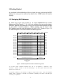
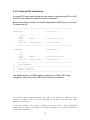
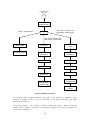
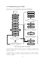
AXEL-X MB8AA3020
On-Chip Code
User Manual
REVISION 1.2
TABLE OF CONTENTS
TABLE OF CONTENTS ............................................................................................................................. 2
LIST OF FIGURES...................................................................................................................................... 3
LIST OF TABLES........................................................................................................................................ 3
1.0 ABOUT THIS MANUAL ..................................................................................................................... 4
1.1 DOCUMENT OVERVIEW ........................................................................................................................ 4
1.2
ACRONYMS .................................................................................................................................. 5
2.0 INTRODUCTION ................................................................................................................................. 6
2.1 BYTE .DATA ORGANIZATION................................................................................................................ 7
2.2 MICRO-COMMANDS .............................................................................................................................. 8
2.3 GETTING STARTED ............................................................................................................................... 9
2.3.1 Assigning MAC Addresses ........................................................................................................... 9
2.3.2 Configuring 10GBE Transmitter and Receiver.......................................................................... 11
2.3.2.1 Configuring Transmit Pre-emphasis....................................................................................... 12
2.3.2.2 Configuring Transmit/Receive Lane and Polarity Swapping.................................................. 13
2.3.2.3 Configuring the Port Configuration Register ......................................................................... 14
2.3.3 Initializing GMII/MII Registers ................................................................................................. 14
2.3.3.1 External PHY Initialization..................................................................................................... 16
2.3.3 Initializing I2C Master Ports ..................................................................................................... 19
3.0 MICRO-ENGINE DESCRIPTION ................................................................................................... 20
3.1 TASK STRUCTURE ............................................................................................................................... 20
3.2 MB8AA3020 INITIALIZATION SEQUENCE ......................................................................................... 21
3.3.1 Initialization Sequence for MII/GMII ....................................................................................... 23
3.3.2 Initialization Sequence for 10GBE............................................................................................ 24
4.0 BUILDING MB8AA3020 FIRMWARE IMAGE ............................................................................. 25
4.1 BUILD PROCEDURE ............................................................................................................................ 25
This document contains confidential information which shall not be reproduced or transferred to other
documents or disclosed to others or used for manufacturing or any other purpose without prior written
permission from FUJITSU Ltd.
All information contained in this document is subject to change without notice. While the information
contained herein is believed to be accurate, such information is preliminary, and should not be relied upon
for accuracy or completeness.
2
LIST OF FIGURES
Figure 1
Figure 2
Figure 3
Figure 4
Field Description MAC Address and EtherType Field ....................................... 9
Initialization Sequence ...................................................................................... 22
Initialization Sequence for MII/GMII Task ...................................................... 23
Initialization Sequence for 10GBE Task........................................................... 24
LIST OF TABLES
Table 1 Data Byte Relationship .......................................................................................... 7
Table 2 Micro-Commands ................................................................................................. 8
Table 3 Task Description .................................................................................................. 20
This document contains confidential information which shall not be reproduced or transferred to other
documents or disclosed to others or used for manufacturing or any other purpose without prior written
permission from FUJITSU Ltd.
All information contained in this document is subject to change without notice. While the information
contained herein is believed to be accurate, such information is preliminary, and should not be relied upon
for accuracy or completeness.
3
1.0 About This Manual
This document is intended to provide configuration description for Fujitsu
MB8AA3020 10Gbps Ethernet switch on chip code.
1.1 Document Overview
The document includes a description of the following:
•
•
•
•
•
•
•
Getting started example
Micro-engine specification
Memory map description
Initialization sequence
Global variable description
Task descriptions
Initialization code block
While all registers can be modified using the On-Chip code these are the main
registers that are supplied by default:
•
•
•
•
•
•
•
•
•
•
•
All setting in the switch configuration registers.
All setting in the port configuration registers.
All port interrupt status registers.
Switch status register.
Buffer management register.
Management port control register.
Host VLAN counter configuration register.
MAC configuration register.
MII/GMII status control register.
Default MAC addresses for the switch and all ports.
Fixed or adaptive gain for receiver equalizer.
The above list while not exhaustive illustrates the programmability of the
MB8AA3020.
This document contains confidential information which shall not be reproduced or transferred to other
documents or disclosed to others or used for manufacturing or any other purpose without prior written
permission from FUJITSU Ltd.
All information contained in this document is subject to change without notice. While the information
contained herein is believed to be accurate, such information is preliminary, and should not be relied upon
for accuracy or completeness.
4
1.2 Acronyms
EEPROM
ENV
GMII
ICB
I/F
IRQ
LAN
MAT
MII
MAC
RAM
VLAN
Electrically Erasable Read Only Memory
Environment
Giga-bit Media Independent Interface
Initialization Code Block
Interface
Interrupt Request
Local Area Network
MAC Address Table
Media Independent Interface
Medium Access Control
Random Access Memory
Virtual Local Area Network
This document contains confidential information which shall not be reproduced or transferred to other
documents or disclosed to others or used for manufacturing or any other purpose without prior written
permission from FUJITSU Ltd.
All information contained in this document is subject to change without notice. While the information
contained herein is believed to be accurate, such information is preliminary, and should not be relied upon
for accuracy or completeness.
5
2.0 Introduction
This section focuses on a step by step example of how to configure and compile
the MB8AA3020 AXEL-X on chip code. It uses the MB8AA3020 AXEL-X
evaluation board as an example, for a more detail description of the MB8AA3020
AXEL-X evaluation board please refer to AXEL-X Evaluation Board Hardware
Manual.
The generic firmware that is included with the Fujitsu MB8AA3020 AXEL-X chip
does not assign MAC addresses to the ports or the chip so at the very least the
user must assign a MAC address for every port as well as the chip address for
the 10GBE switch to function properly.
In addition to this the user must decide whether to use fixed or dynamic gain
before compiling the firmware.
Before we begin our example we must first understand how the byte structure is
organized in the assembly files as well as understand the various microcommands. Section 2.1 Byte .data Organization describes the byte structure
organization while Section 2.2 Micro-commands describes the micro-commands.
This document contains confidential information which shall not be reproduced or transferred to other
documents or disclosed to others or used for manufacturing or any other purpose without prior written
permission from FUJITSU Ltd.
All information contained in this document is subject to change without notice. While the information
contained herein is believed to be accurate, such information is preliminary, and should not be relied upon
for accuracy or completeness.
6
2.1 Byte .data Organization
In order to begin configuring the on chip code firmware we must first understand
how the byte structure is set up in the assembly files.
Below is an example of a factious symbol and the .data fields associated with the
symbol.
// --------------------------------------------------------------//
Example of .data description
// --------------------------------------------------------------Example_symbol_0:
// Example of symbol
.data
0x0123
// byte 1= 01; byte 0 = 23
.data
0x4567
// byte 3= 45; byte 2 = 67
.data
0x89AB
// byte 5= 89; byte 4 = AB
.data
0xCDEF
// byte 7= CD; byte 6 = EF
// --------------------------------------------------------------//
Example of .data description
// ---------------------------------------------------------------
The organization of the .data fields always start with byte 1 and byte 0
corresponding to the first data field, byte 3 and byte 2 corresponding to the
second data field and so on. Table 1 Data Byte Relationship describes the Data
Byte relationship.
Data
.data
.data
.data
.data
Bytes
Byte 1 Byte 0
Byte 3, Byte 2
Byte 5, Byte 4
Byte 7, Byte 6
Table 1 Data Byte Relationship
This document contains confidential information which shall not be reproduced or transferred to other
documents or disclosed to others or used for manufacturing or any other purpose without prior written
permission from FUJITSU Ltd.
All information contained in this document is subject to change without notice. While the information
contained herein is believed to be accurate, such information is preliminary, and should not be relied upon
for accuracy or completeness.
7
2.2 Micro-commands
Listed in Table 2 is a list of commonly used micro-commands that are executed
by the MB8AA3020 micro-engine.
Micro-command
Description
.align_block
Align the block frame
.skip
Skip the current
instruction
.data
.data_ref
Assigns a 16 bit value
to the data
The data is reference
to a pointer that is
defined by the user
using “:”
Example
N/A
.data 0x1234
.skip
.data 0x4567
.data <16 bit value>
.data_ref ICB_PCS_0
ICB_PCS_0:
.data 0x1234
.data 0x4567
.skip
.skip
Table 2 Micro-Commands
This document contains confidential information which shall not be reproduced or transferred to other
documents or disclosed to others or used for manufacturing or any other purpose without prior written
permission from FUJITSU Ltd.
All information contained in this document is subject to change without notice. While the information
contained herein is believed to be accurate, such information is preliminary, and should not be relied upon
for accuracy or completeness.
8
2.3 Getting Started
As mentioned in the introduction at the very least the user must set up the MAC
address for every port as well as the chip for the 10GBE switch to function
properly.
2.3.1 Assigning MAC Addresses
By default the source code provided by the Fujitsu MB8AA3020 has a MAC
address and EtherType of 0. So at the very minimum the user must assign a
valid MAC address and Ethertype to every port and the station address in order
for the switch to function properly. These variables can be found in the
MAC_address.asm file under the symbol Hst_Adr_[0-23]. Shown in Figure 1 is
the field description for the MAC address and EtherType field.
Byte 7
Byte 6
Byte 5
Byte 4
Byte 3
Byte 2
Byte 1
Byte 0
description
Hst_Adr_0
MAC Address xx:xx:xx:xx:xx:xx
N/A
Port 0
Hst_Adr_1
Hst_Adr_2
Hst_Adr_3
Hst_Adr_4
MAC Address xx:xx:xx:xx:xx:xx
N/A
Port 1
MAC Address xx:xx:xx:xx:xx:xx
N/A
Port 2
MAC Address xx:xx:xx:xx:xx:xx
MAC Address xx:xx:xx:xx:xx:xx
N/A
N/A
Port 3
Port 4
MAC Address xx:xx:xx:xx:xx:xx
MAC Address xx:xx:xx:xx:xx:xx
N/A
N/A
Port 5
Port 6
Hst_Adr_5
Hst_Adr_6
Hst_Adr_7
Hst_Adr_8
Hst_Adr_9
Hst_Adr_10
Hst_Adr_11
Hst_Adr_12
Hst_Adr_13
Hst_Adr_14
MAC Address xx:xx:xx:xx:xx:xx
N/A
Port 13
MAC Address xx:xx:xx:xx:xx:xx
N/A
Port 14
Hst_Adr_15
Hst_Adr_16
Hst_Adr_17
Hst_Adr_18
Hst_Adr_19
Hst_Adr_21
Hst_Adr_23
MAC
MAC
MAC
MAC
MAC
MAC
MAC
N/A
N/A
N/A
N/A
N/A
N/A
N/A
Port
Port
Port
Port
Port
Port
Port
MAC Address xx:xx:xx:xx:xx:xx
N/A
Port 7
MAC Address xx:xx:xx:xx:xx:xx
N/A
Port 8
MAC Address xx:xx:xx:xx:xx:xx
N/A
Port 9
MAC Address xx:xx:xx:xx:xx:xx
N/A
Port 10
MAC Address xx:xx:xx:xx:xx:xx
N/A
Port 11
MAC Address xx:xx:xx:xx:xx:xx
N/A
Port 12
Address
Address
Address
Address
Address
Address
Address
xx:xx:xx:xx:xx:xx
xx:xx:xx:xx:xx:xx
xx:xx:xx:xx:xx:xx
xx:xx:xx:xx:xx:xx
xx:xx:xx:xx:xx:xx
xx:xx:xx:xx:xx:xx
xx:xx:xx:xx:xx:xx
15
16
17
19
20
21
23
Reg_STA
MAC Address xx:xx:xx:xx:xx:xx
Ethertype
Register Station
Address
Figure 1 Field Description MAC Address and EtherType Field
This document contains confidential information which shall not be reproduced or transferred to other
documents or disclosed to others or used for manufacturing or any other purpose without prior written
permission from FUJITSU Ltd.
All information contained in this document is subject to change without notice. While the information
contained herein is believed to be accurate, such information is preliminary, and should not be relied upon
for accuracy or completeness.
9
Note: It is important to note that in order for the switch to function properly
a valid MAC address must be assigned for every port and station address.
Below is an excerpt from the MAC_address.asm file. The first data field is two
bytes long and refer to the EtherType, the rest of the .data field refer to the MAC
address. The EtherType is only used in the REG_STA address there is no
requirement to assign an EtherType for the ports.
// --------------------------------------------------------------//
MAC Addresses: API Access
// --------------------------------------------------------------REG_STA:
.data
.data
.data
.data
0x0000
0x0000
0x0000
0x0000
//
//
//
//
//
aa:bb:cc:dd:ee:ff
type = 0x0000
msw = ee_ff
lsw2 = cc_dd
lsw1 = aa_bb
Example: MAC Address Assignment to REG_STA
Below is an example where a MAC address of 00-11-F5-76-82-61 and an
EtherType of 88B5 to the REG_STA.
// --------------------------------------------------------------//
MAC Addresses: API Access
// --------------------------------------------------------------Reg_STA:
.data
.data
.data
.data
// 00:11:F5:76:82:61
0x88b5
// type = 0x88b5
0x8261
// msw = 82_61
0xF576
// lsw2 = F5_76
0x0011
// lsw1 = 00_11
Example: MAC Address Assignment to PORT 0
Below is an example where a MAC address of 00-11-F5-AB-CD-EF is applied to
port 0. Recall that for ports an EtherType entry is not required.
// --------------------------------------------------------------//
MAC Addresses:
Port MAC Control
// --------------------------------------------------------------Hst_Adr_0:
.data
.data
.data
.data
// 00:11:F5:AB:CD:EF
0x0000
0xCDEF
0xF5AB
0x0011
This document contains confidential information which shall not be reproduced or transferred to other
documents or disclosed to others or used for manufacturing or any other purpose without prior written
permission from FUJITSU Ltd.
All information contained in this document is subject to change without notice. While the information
contained herein is believed to be accurate, such information is preliminary, and should not be relied upon
for accuracy or completeness.
10
2.3.2 Configuring 10GBE Transmitter and Receiver
Fujitsu MB8AA3020 10GBE switch has an integrated 5-TAP FIR filter used for
additional pre-emphasis and a 2nd order linear amplifier used for receiver
equalization. The details of which can be found in AXEL-X MB8AA3020 PCS
Register Specification.
Before programming the on-chip the user must decide on the following
configuration parameters:
•
•
•
•
•
•
•
XAUI mode of operation of XFI mode of operation for XFI 10GBE ports.
Transmit pre-emphasis co-efficient to be used.
Fixed gain or adaptive gain equalization for the receiver
Transmitter lane swapping.
Transmitter polarity swapping.
Receiver lane swapping.
Receiver polarity swapping.
Below is an example of how to modify the on-chip code for adaptive gain.
Example: Modification of Receiver Gain.
In order to modify the receiver for fixed or dynamic gain open the Makefile.
Below is an excerpt from the Makefile.
AWK
= gawk
PCS_AWK
= ../bin/ICB_PCS.awk
PCS_CONF
= ./axelx_pcs_phy_cfg_adaptive_eval_board.txt
#PCS_CONF
=
../../../../../register/axelx_pcs_phy_cfg_adaptive_eval_board.txt
#PCS_CONF
=
../../../../../register/axelx_pcs_phy_cfg_fixed_eval_board.txt
By default the on chip code is set up to use adaptive gain. If you wish to use fix
gain comment out the line “PCS_CONF
axelx_pcs_phy_cfg_adaptive_eval_board.txt” and uncomment out the fixed gain
line “PCS_CONF axelx_pcs_phy_cfg_fixed_eval_board.txt”.
This document contains confidential information which shall not be reproduced or transferred to other
documents or disclosed to others or used for manufacturing or any other purpose without prior written
permission from FUJITSU Ltd.
All information contained in this document is subject to change without notice. While the information
contained herein is believed to be accurate, such information is preliminary, and should not be relied upon
for accuracy or completeness.
11
Below is an example of a Makefile that uses fixed gain.
AWK
PCS_AWK
#PCS_CONF
PCS_CONF
= gawk
= ../bin/ICB_PCS.awk
= ./axelx_pcs_phy_cfg_adaptive_eval_board.txt
= ./register/axelx_pcs_phy_cfg_fixed_eval_board.txt
Note: Please remember to assign the right path to these files. Without the
correct path the Makefile will not compile properly.
For adaptive gain you do not need to modify any receiver co-efficient since they
are determined automatically using the adaptive equalization algorithm, this is
not the case for fixed gain. For fixed gain you need to modify the following the
gain co-efficient. The file that need to be modified is
axelx_pcs_phy_cfg_fixed_eval_board.txt and the procedure used to modify the
fixed gain parameters can be found in AXEL-X MB8AA3020 PCS Register
Specification.
2.3.2.1 Configuring Transmit Pre-emphasis
The default transmit pre-emphasis parameters can be found in either
axelx_pcs_phy_cfg_adaptive_eval_board.txt or
axelx_pcs_phy_cfg_fixed_eval_board.txt depending if the user is using fixed or
adaptive gain. Below is an excerpt from the
axelx_pcs_phy_cfg_adaptive_eval_board.txt transmit pre-emphasis co-efficients
for port 0. These transmit pre-emphasis co-efficients are optimized specifically
for the AXEL-X evaluation board and may not be appropriate for all applications.
PORT 00
# mode
value
M1
5
# step addr
data
S2 0x0007 0x0001 #S2 0xc002 0x000f #@
S2 0xc003 0x86a0 #S2 0xc000 0x00ff #S2 0x0000 0x8000 #S2 0xc010 0x03f0 #@
S2 0xc011 0x03f0 #@
S2 0xc012 0x0330 #@
S2 0xc013 0x13f1 #@
S2 0xc014 0x0000 #@
S2 0xc015 0x03f0 #@
S2 0xc016 0x03f0 #@
S2 0xc017 0x0330 #@
#@
###PCS_CTL2
XL_LANE_SWAP_CTL
PHY_PLL_MODE_CTL
PHY_PWR_DOWN_CTL
PCS_CTL1
PHY_TX0_EQ_CFG0
PHY_TX0_EQ_CFG1
PHY_TX0_EQ_CFG2
PHY_TX0_EQ_CFG3
PHY_TX0_EQ_CFG4
PHY_TX1_EQ_CFG0
PHY_TX1_EQ_CFG1
PHY_TX1_EQ_CFG2
Select port number (00~19).
Select adaptive mode.
Select XAUI mode.
Set Tx polarity swap.
Set PHY PLL mode.
Assert PHY Tx/Rx PD signals.
Reset PCS.
Set Tx lane-0 tap-0 with +63(0).
Set Tx lane-0 tap-1 with +63(0).
Set Tx lane-0 tap-2 with +51(0).
Set Tx lane-0 tap-3 with -63(1).
Set Tx lane-0 tap-4 with +0(0).
Set Tx lane-1 tap-0 with +63(0).
Set Tx lane-1 tap-1 with +63(0).
Set Tx lane-1 tap-2 with +51(0).
This document contains confidential information which shall not be reproduced or transferred to other
documents or disclosed to others or used for manufacturing or any other purpose without prior written
permission from FUJITSU Ltd.
All information contained in this document is subject to change without notice. While the information
contained herein is believed to be accurate, such information is preliminary, and should not be relied upon
for accuracy or completeness.
12
S2 0xc018 0x13f1 #@ PHY_TX1_EQ_CFG3
Set
S2 0xc019 0x0000 #@ PHY_TX1_EQ_CFG4
Set
S2 0xc01a 0x03f0 #@ PHY_TX2_EQ_CFG0
Set
S2 0xc01b 0x03f0 #@ PHY_TX2_EQ_CFG1
Set
S2 0xc01c 0x0330 #@ PHY_TX2_EQ_CFG2
Set
S2 0xc01d 0x13f1 #@ PHY_TX2_EQ_CFG3
Set
S2 0xc01e 0x0000 #@ PHY_TX2_EQ_CFG4
Set
S2 0xc01f 0x03f0 #@ PHY_TX3_EQ_CFG0
Set
S2 0xc020 0x03f0 #@ PHY_TX3_EQ_CFG1
Set
S2 0xc021 0x0330 #@ PHY_TX3_EQ_CFG2
Set
S2 0xc022 0x13f1 #@ PHY_TX3_EQ_CFG3
Set
S2 0xc023 0x0000 #@ PHY_TX3_EQ_CFG4
Set
S2 0xc052 0x0000 #PHY_TX23_MON_CTL Set Tx
Tx lane-1 tap-3 with
Tx lane-1 tap-4 with
Tx lane-2 tap-0 with
Tx lane-2 tap-1 with
Tx lane-2 tap-2 with
Tx lane-2 tap-3 with
Tx lane-2 tap-4 with
Tx lane-3 tap-0 with
Tx lane-3 tap-1 with
Tx lane-3 tap-2 with
Tx lane-3 tap-3 with
Tx lane-3 tap-4 with
lane-3 MON_CTL[6]=0.
-63(1).
+0(0).
+63(0).
+63(0).
+51(0).
-63(1).
+0(0).
+63(0).
+63(0).
+51(0).
-63(1).
+0(0).
In order to modify these parameters please follow the procedure outlines in the
AXEL-X MB8AA3020 PCS Register Specification.
2.3.2.2 Configuring Transmit/Receive Lane and Polarity Swapping
By default the transmit polarity is swapped on the AXEL-X evaluation board for
XAUI ports (i.e ports 0, 3-4, 7-19) and transmitter and receiver polarity are
swapped for XFI ports (i.e ports 1, 2, 5, 6).
This may not be appropriate for all applications. In order to modify the lane or
polarity swapping use XL LANE POLARITY SWAP CONTROL REGISTER (i.e
0xC002) as described in Table 49 of AXEL-X MB8AA3020 PCS Register
Specification.
Below is an example where the transmit XAUI ports lanes are swapped but the
transmit polarity is not swapped. This parameter can be found in both the
axelx_pcs_phy_cfg_adaptive_eval_board.txt or
axelx_pcs_phy_cfg_fixed_eval_board.txt file.
S2
0xc002 0x0030 #@ XL_LANE_SWAP_CTL
Set Tx polarity swap.
This document contains confidential information which shall not be reproduced or transferred to other
documents or disclosed to others or used for manufacturing or any other purpose without prior written
permission from FUJITSU Ltd.
All information contained in this document is subject to change without notice. While the information
contained herein is believed to be accurate, such information is preliminary, and should not be relied upon
for accuracy or completeness.
13
2.3.2.3 Configuring the Port Configuration Register
By default all 10GBE ports are disabled with the generic firmware version. In
order to enable the ports by default follow the instructions below.
Below is an excerpt from the file ICB_reg.asm. In this file the first two .data fields
of the pointer ICB_Default_0 controls the Port Configuration Register (i.e
base+000h) as described in AXEL-X MB8AA3020 Register Specification.
ICB_Default_0:
.data
.data
.data
.data_ref
// all @ Port Config
0x0001
// 0xd2000001
0xd100
// [31] Port Reset
0x3800
ICB_Default_1
In order to change the port from the default disable state to a forwarding state
bits [16:17] in the port configuration register needs to change from their current
state of 00 to 11. This is illustrated below:
ICB_Default_0:
.data
.data
.data
.data_ref
// all @ Port Config
0x0001
// 0xd2000001
0xd103
// [31] Port Reset
0x3800
ICB_Default_1
2.3.3 Initializing GMII/MII Registers
The initialization of the MII/GMII interface is dependent on the user environment.
By default the generic firmware version initialization sequence for the GBE
interface is based on the AXEL-X evaluation board which has two external PHYs
connected to the AXEL-X’s MII/GMII ports. So by default the generic firmware
initializes these two 10/100/GBE ports as GMII and assumes that there is an
external PHY connected to these ports. While this is appropriate for the AXEL-X
evaluation board it may not be suitable for all applications.
This document contains confidential information which shall not be reproduced or transferred to other
documents or disclosed to others or used for manufacturing or any other purpose without prior written
permission from FUJITSU Ltd.
All information contained in this document is subject to change without notice. While the information
contained herein is believed to be accurate, such information is preliminary, and should not be relied upon
for accuracy or completeness.
14
Below is an excerpt from the Firmware.asm file which shows the initialization of
the two Ethernet ports to GMII.
task24_bp3:
// Firmware Main Task
// bp + 4: Port Mode
.data_ref
ICB_Post_Core_0
.data
0x0000
// mode[23],0,[21],0, 0000
//
for 23/21, 0: GMII, 1:MII
The following configuration possibilities apply.
If the user wishes to modify both ports to MII the following modification needs to
be performed:
Example: Both ports converted to MII
task24_bp4:
.data_ref
.data
ICB_Port_Core_0
0x0a00
Only port 21 converted to MII but port 23 left as GMII the following modification
needs to be done.
Example: Port 21 is MII Port 23 is GMII
task24_bp4:
.data_ref
.data
ICB_Port_Core_0
0x0200
Port 21 is GMII but port 23 is MII the following modification needs to be done.
Example: Port 21 is GMII Port 23 is MII
task24_bp4:
.data_ref
.data
ICB_Port_Core_0
0x0800
This document contains confidential information which shall not be reproduced or transferred to other
documents or disclosed to others or used for manufacturing or any other purpose without prior written
permission from FUJITSU Ltd.
All information contained in this document is subject to change without notice. While the information
contained herein is believed to be accurate, such information is preliminary, and should not be relied upon
for accuracy or completeness.
15
2.3.3.1 External PHY Initialization
If external PHY are connected and the user wants to configure these PHYs in MII
mode then the following modification must be performed.
Below is an excerpt of task28 and task29 responsible for MDIO ports found in the
Firmware.asm file.
// --------------------------------------------------------------task28_bp3:
// bp + 3
.skip
.data
.skip
.data_ref
// MDIO Port-1
0x0000
// Interface Core ICB
ICB_MDIO_GMII_0
// Interface ICB
// --------------------------------------------------------------task29_bp3:
// bp + 3
.skip
.data
.skip
.data_ref
// MDIO Port-2
0x0000
// Interface Core ICB
ICB_MDIO_GMII_0
// Interface ICB
// --------------------------------------------------------------//
Task Dependency
// --------------------------------------------------------------//
MDIO-1 -> Port-21
//
MDIO-2 -> Port-23
// ---------------------------------------------------------------
The default setting is for GMII however to convert from GMII to MII simply
change the .data_ref text from GMII to MII. Below is an example:
This document contains confidential information which shall not be reproduced or transferred to other
documents or disclosed to others or used for manufacturing or any other purpose without prior written
permission from FUJITSU Ltd.
All information contained in this document is subject to change without notice. While the information
contained herein is believed to be accurate, such information is preliminary, and should not be relied upon
for accuracy or completeness.
16
Example: Converting MDIO ports from GMII to MII
// --------------------------------------------------------------task28_bp3:
// bp + 3
.skip
.data
.skip
.data_ref
// MDIO Port-1
0x0000
// Interface Core ICB
ICB_MDIO_MII_0
// Interface ICB
// --------------------------------------------------------------task29_bp3:
// bp + 3
.skip
.data
.skip
.data_ref
// MDIO Port-2
0x0000
// Interface Core ICB
ICB_MDIO_MII_0
// Interface ICB
// --------------------------------------------------------------//
Task Dependency
// --------------------------------------------------------------//
MDIO-1 -> Port-21
//
MDIO-2 -> Port-23
// ---------------------------------------------------------------
In addition to the PHY initialization the ICB_mdio.asm file needs to be modified
based on the PHY initialization sequence. This is especially true if the MDIO
interface is connected to the PHY because the PHY address is embedded in the
initialization code.
Using the AXEL-X evaluation board as an example port21 is polling PHY register
1 at PHY address 0 via MDIO-1 and port 23 is polling PHY register 1 at PHY
address 0 via MDIO-2.
Below is an excerpt of the Firmware.asm showing this:
// --------------------------------------------------------------task21_bp3:
// Task Port-21
// bp + 3: Port IRQ Service Required vector, Mode
.data
0x4003
// Use MDIO-0 for polling, Mode = 3
.data
0x0000
// Link up Check Threshold
This document contains confidential information which shall not be reproduced or transferred to other
documents or disclosed to others or used for manufacturing or any other purpose without prior written
permission from FUJITSU Ltd.
All information contained in this document is subject to change without notice. While the information
contained herein is believed to be accurate, such information is preliminary, and should not be relied upon
for accuracy or completeness.
17
// --------------------------------------------------------------task23_bp3:
// Task Port-23
// bp + 3: Port IRQ Service Required vector, Mode
.data
0x8003
// Use MDIO-2 for polling, Mode = 3
.data
0x0000
// Link up Check Threshold
.data
0x0801
// [11] Port Security Violation,
[0] Link Fault
.data
0x0000
// ---------------------------------------------------------------
By default the on chip code poll the PHY status check with link fault handler.
This may not be appropriate for all situations because the user may not have a
PHY or the MDIO may not be connected up to the PHY. If this is the case in then
you will want to bypass the PHY status check by enabling Mode=2. Below is an
example where the PHY status
Example of MDIO with PHY status disable
// --------------------------------------------------------------task21_bp3:
// Task Port-21
// bp + 3: Port IRQ Service Required vector, Mode
.data
0x4002
// Use MDIO-0 for polling, Mode = 2
.data
0x0000
// Link up Check Threshold
// --------------------------------------------------------------task23_bp3:
// Task Port-23
// bp + 3: Port IRQ Service Required vector, Mode
.data
0x8002
// Use MDIO-2 for polling, Mode = 2
.data
0x0000
// Link up Check Threshold
.data
0x0801
// [11] Port Security Violation,
[0] Link Fault
.data
0x0000
// ---------------------------------------------------------------
Lastly by default of the PHY address on the AXEL-X evaluation is 0 for both port
21 and port 23 however this is not universal for all design. In order to change
this refer to Firmware.asm file task21_bp6 and task_23_bp6.
This document contains confidential information which shall not be reproduced or transferred to other
documents or disclosed to others or used for manufacturing or any other purpose without prior written
permission from FUJITSU Ltd.
All information contained in this document is subject to change without notice. While the information
contained herein is believed to be accurate, such information is preliminary, and should not be relied upon
for accuracy or completeness.
18
Below is an excerpt from this file:
// --------------------------------------------------------------task21_bp3:
// Task Port-21
// bp + 6: Link Up Wait Time
.data
40
// 10ms
.data
0
// 0ms
.data
0x0000
.data
0x6006
// PHY Addr=0, PHY Register=1
// --------------------------------------------------------------task23_bp3:
// Task Port-23
// bp + 6: Link Up Wait Time
.data
40
// 10ms
.data
0
// 0ms
.data
0x0000
.data
0x6006
// PHY Addr=0, PHY Register=1
// ---------------------------------------------------------------
2.3.3 Initializing I2C Master Ports
Initialization of the I2C master ports is essential for proper operation of I2C
master ports on AXEL-X chip. By default the on-chip code initializes I2C port 2
as the master but user may use both I2C ports 1 and port 2 as master ports
which would require both to be initialized properly.
Note: No initialization of I2C slave ports is required.
This document contains confidential information which shall not be reproduced or transferred to other
documents or disclosed to others or used for manufacturing or any other purpose without prior written
permission from FUJITSU Ltd.
All information contained in this document is subject to change without notice. While the information
contained herein is believed to be accurate, such information is preliminary, and should not be relied upon
for accuracy or completeness.
19
3.0 Micro-Engine Description
Fujitsu MB8AA3020 10Gbps Ethernet switch uses an integrated 312.5 MHz core,
32KB RAM micro-engine to decoded micro-commands sent to the switch via a
user designated Ethernet management interface. The micro-commands are
encapsulated into an Ethernet frame and decoded by the micro-engine.
The use of the micro-engine gives users’ the added flexibility in programming the
MB8AA3020 and at the same time reducing software development time.
3.1 Task Structure
There are a total of 32 individual tasks which are described in Table 3. The
memory is context switched so each tasks uses the entire 2KBx64bytes of
memory.
Task Number
0-19
20
21
Thread Name
task_port
task_none
task_port_1g
Initial Task State
Ready
Sleep
Ready
22
23
task_none
task_port_1g
Sleep
Ready
24
25
26
Firmware
task_none
task_i2c
Run
Sleep
Ready
27
task_i2c
Ready
28
task_mdio
Ready
29
task_mdio
Ready
30
task_test
Sleep
31
task_RTC
Ready
Description
10G port monitor
Reserved
MII/GMII port
monitor
Reserved
MII/GMII port
monitor
Firmware Main
Reserved
I2C Port-1
Handler
I2C Port-2
Handler
MDIO Port-1
Handler
MDIO Port-2
Handler
For Firmware Test
Purposes
Real Time Clock
Table 3 Task Description
This document contains confidential information which shall not be reproduced or transferred to other
documents or disclosed to others or used for manufacturing or any other purpose without prior written
permission from FUJITSU Ltd.
All information contained in this document is subject to change without notice. While the information
contained herein is believed to be accurate, such information is preliminary, and should not be relied upon
for accuracy or completeness.
20
3.2 MB8AA3020 Initialization Sequence
Shown in Figure 2 is the initialization sequence for the MB8AA3020 Fujitsu
switch.
Power
On
Port Reset/MAC
Address
Download firmware
Firmware is downloaded
from EEPROM
GMII/MII Interface
Reset
This process is skip
when the AXEL-X has
been warm restarted.
Start Multi-task
Environment
Device ICB
Firmware Task
ICB_reg.asm
STATIC
Set IRQ Handler
CONFIGURABLE
Set Buffer
Management
Register
Firmware.asm
task_24: bp+3
byte4 - byte7
Set Switch
Configuration
Register
Firmware.asm
task_24: bp+3
byte0 - byte 3
Set MAC
Addresses
MAC addresses are
programmed by user in
MAC_addres.asm file.
VLAN ICB
Disable Ports
MAC Address
Table ICB
task_24: Firmware
Set Initialization Flag
Complete
This document contains confidential information which shall not be reproduced or transferred to other
documents or disclosed to others or used for manufacturing or any other purpose without prior written
permission from FUJITSU Ltd.
All information contained in this document is subject to change without notice. While the information
contained herein is believed to be accurate, such information is preliminary, and should not be relied upon
for accuracy or completeness.
21
From MAC Address
Table ICB
Set Initialization
Completion Flag
task_[26:27]: Firmware.asm
task_[28:29]: Firmware.asm
task_24: Firmware.asm
task_[0-19]: Firmware.asm
task_[21:23]: Firmware.asm
Port Core ICB
Port Tasks
I/F (I2C/MDIO)
Task
API Handler Ready
Resolve Task
Dependency
Resolve Task
Dependency
Port ICB
I/F Reg ICB
PCS ICB
I/F ICB
I/F ICB Done
Wait Link Up
Set Initialization
Completion Flag
Set Initialization
Completion Flag
Sleep and wait
request
Figure 2 Initialization Sequence
This document contains confidential information which shall not be reproduced or transferred to other
documents or disclosed to others or used for manufacturing or any other purpose without prior written
permission from FUJITSU Ltd.
All information contained in this document is subject to change without notice. While the information
contained herein is believed to be accurate, such information is preliminary, and should not be relied upon
for accuracy or completeness.
22
3.3.1 Initialization Sequence for MII/GMII
Shown in Figure 3 is the initialization sequence for task_[21:23] MII/GMII task.
Start
Wait_Count = 0
Execute Port ICB
Wait Link Down
Polling Timer
Wait_Count++
Wait_Count = 0
Wait Timer A = 10ms
Wait_Count++
Check Link
Status
Check Link
Status
Down
Down
Up
Yes
Threshold=1
Wait_Count < Threshold
Threshold=1
Wait_Count < Threshold
No
Wait Timer B = 10ms
Execute Link Fault
ICB
Execute Link-up
ICB A
Wait Timer C = 10ms
Execute Link-up
ICB B
Enable Link Fault Handler
End
Figure 3 Initialization Sequence for MII/GMII Task
This document contains confidential information which shall not be reproduced or transferred to other
documents or disclosed to others or used for manufacturing or any other purpose without prior written
permission from FUJITSU Ltd.
All information contained in this document is subject to change without notice. While the information
contained herein is believed to be accurate, such information is preliminary, and should not be relied upon
for accuracy or completeness.
23
3.3.2 Initialization Sequence for 10GBE
Shown in Figure 4 is the initialization sequence for the 10GBE task.
Execute PCS
Restart ICB B
Start
Wait Timer B
Execute Port ICB
Execute PCS Link
up ICB
Execute PCS ICB
Wait Time for
GearBox Reset
Execute Link up ICB
GearBox Reset
Enable Link
Fault Handler
Wait Count = 0
Execute PCS
Restart ICB A
Wait Timer C
Wait Count ++
PCS Status Clear
Wait Time
Yes
Read PCS Status 2
(clear link handler bit-11, 10)
Check Link Status
No
Wait Count = 0
Read PCS Status 2
Wait Timer A
Wait Count ++
Threshold=1
Wait_Count < Threshold
Check Link Status
Down
Execute Link Fault
ICB
Up
Yes
Threshold=1
Wait_Count < Threshold
No
End
Figure 4 Initialization Sequence for 10GBE Task
This document contains confidential information which shall not be reproduced or transferred to other
documents or disclosed to others or used for manufacturing or any other purpose without prior written
permission from FUJITSU Ltd.
All information contained in this document is subject to change without notice. While the information
contained herein is believed to be accurate, such information is preliminary, and should not be relied upon
for accuracy or completeness.
24
4.0 Building MB8AA3020 Firmware Image
This section describes how to build the image for MB8AA3020. These same
instructions can be found in the ReadMe file of the On-Chip-Code released with
the chip.
4.1 Build Procedure
In order to compile the MB8AA3020 code the following is needed:
•
•
•
MB8AA3020 on chip source code described above.
MB8AA3020 Make file.
GNU Compiler Collection (i.e gcc)
The procedure for building the MB8AA3020 firmware image is described below:
1. As stated in Section 2.3.1 Assigning MAC Addresses the user needs to
assign an appropriate MAC address for the chip as well as each port.
This is done by editing the MAC_address.asm file.
2. Choose either fixed gain (i.e axel_pcs_phy_cfg_fixed_eval_board.txt) or
adaptive gain (i.e axel_pcs_phy_cfg_adaptive_eval_board.txt) in the
Makefile.
3. Type make on the command line.
Two files named firmware.dat and firmware.sym will be generated and placed in
the obj directory. Firmware.dat is the file that will be downloaded into the
MB8AA3020’s EEPROM.
This document contains confidential information which shall not be reproduced or transferred to other
documents or disclosed to others or used for manufacturing or any other purpose without prior written
permission from FUJITSU Ltd.
All information contained in this document is subject to change without notice. While the information
contained herein is believed to be accurate, such information is preliminary, and should not be relied upon
for accuracy or completeness.
25