1
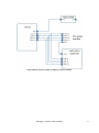
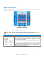
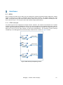
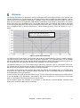
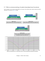
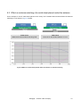
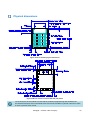
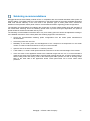
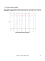
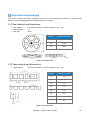
BT121 BLUETOOTH SMART READY MODULE DATA SHEET Wednesday, 13 May 2015 Document Version: 1.2 Copyright © Silicon Labs All rights reserved. Silicon Labs assumes no liability or responsibility for any errors, mistakes or inaccuracies in content. Silicon Labs reserves the right to change products or specifications without notice, and does not make any commitment to update the information herein. Silicon Labs’ products are not authorized for use as critical components in life support devices or systems. BGScript™ is a trademark of Silicon Labs. The Bluetooth® word mark and logos are registered trademarks owned by the Bluetooth® SIG, Inc. USA. All other trademarks and trade names listed herein belong to their respective owners. Information is subject to change without notice. Bluegiga – A Silicon Labs Company VERSION HISTORY Date Edited Comment 1.0 First release of document 1.1 Minor updates 1.2 Minor updates Bluegiga – A Silicon Labs Company TABLE OF CONTENTS BT121 overview 6 1.1 Key Features 6 1.2 Typical applications 7 1.3 Block diagram 7 Design guidelines 8 2.1 PCB layout recommendations 8 2.2 Power supply recommendations 8 2.3 Software application related options 8 2.4 Firmware updating related recommendations 8 Pin-out description 10 3.1 Power, ground, reset, RF and boot loader pins 10 3.2 GPIO pins 11 Power control 12 4.1 Power supply requirements 12 4.2 Power saving functionality 12 4.3 Reset 14 4.4 Recovery mode 14 4.5 Clock signals 14 Interfaces 15 5.1 GPIO 15 5.2 UART 16 5.3 I2C 16 5.4 SPI 16 5.5 ADC 16 5.6 DAC 16 5.7 Real-time clock 16 5.8 Microcontroller programming interface 16 Antenna 17 6.1 Effect on antenna matching of a plastic sheet placed near the antenna 18 6.2 Effect on antenna matching of a metal sheet placed under the antenna 19 6.3 Effect on antenna matching of a metal sheet placed against the end of the module 20 6.4 Measured antenna efficiency 21 6.5 Measured 2D radiation patterns 22 6.6 Measured 3D radiation patterns 24 Bluetooth Stack Software 25 Host interface 26 Bluegiga – A Silicon Labs Company 4 8.1 UART 26 Connection examples 27 9.1 Connecting an external host using the UART interface 27 9.2 Connecting an external device using SPI interface 28 9.3 Connecting an external device using I2C interface 29 Electrical characteristics 30 10.1 Absolute maximum ratings 30 10.2 Recommended operating conditions 30 10.3 Logic signal characteristics 31 RF Characteristics 34 11.1 Supported frequencies and channels 34 11.2 Typical receiver sensitivity 34 11.3 Transmitter output power 34 11.4 Carrier frequency accuracy 34 13.1 Physical dimensions 35 Soldering recommendations 37 Soldering profile example 38 Tape and reel packaging 39 14.1 Reel material and dimensions 39 14.2 Tape material and dimensions 39 14.3 Tape and reel box dimensions 40 14.4 Module orientation in tape 40 Certifications 41 15.1 CE 41 15.2 FCC and IC 41 Ordering information 45 Contact Information 46 Bluegiga – A Silicon Labs Company 5 BT121 overview BT121 is a Bluetooth Smart Ready module targeted for applications that require both Bluetooth Smart and Classic connectivity. It can connect to legacy devices that only support Bluetooth SPP or Apple ® iAP2 profiles as well to devices that support Bluetooth Smart. BT121 integrates a high performance Bluetooth radio, a lowpower ARM Cortex micro-controller and a Bluegiga Bluetooth Smart Ready stack software marking it extremely easy-to-use as no RF or Bluetooth software development is needed. BT121 can be used as a modem together with a separate host MCU, but applications can also be embedded into the built-in ARM® Cortex® MCU with the Bluegiga BGScriptTM scripting language. 1.1 Key Features Bluetooth features Hardware interfaces Bluetooth 4.1 Smart Ready compliant UART host interface Master and slave modes 2 x SPI, UART and 2 x I2C peripheral interfaces Up to 6 x BR/EDR connections Up to 22 x GPIO with interrupts Up to 7 x BLE connections 4 x 12-bit ADC and 2 x 12-bit DAC* 1 x BR/EDR + 7 simultaneously Internal temperature sensor* Internal battery voltage measurement option* Clock generator* RTC with calendar* x BLE connections Radio features Integrated antenna TX Power +12 dBm with Bluetooth BR/EDR o +10 dBm with Bluetooth LE RX Sensitivity o Microcontroller o -96 dBm 200-400 meter LoS range ARM Cortex M0 48 Mhz 16kB RAM 128kB flash Electrical characteristics Software features Integrated Bluetooth Smart Ready Stack SPP, iAP2, GATT over BR Bluetooth profiles Any GATT based Bluetooth Smart profile 1000 kbps throughput over SPP 150 kbps throughput over iAP2 100 kbps throughput over BLE BGAPITM serial protocol API over UART for modem usage BGLIBTM host API/library which implements BGAPI serial protocol BGScriptTM scripting language for standalone usage Profile ToolkitTM for creating GATT based services Supply voltage: 2.2V to 3.6V Supply voltage: 2.4V to 3.6V when using ADC Environmental and regulatory Temperature range: -40C to +85C Bluetooth, CE, FCC and IC, Japan and South-Korea qualified* Dimensions: W x L x H: 11.0 mm x 13.9 mm x 2.2 mm *) Feature not implemented on engineering samples and engineering samples are not qualified Bluegiga – A Silicon Labs Company 6 1.2 Typical applications BT121 can be used in a wide variety of applications such as health and fitness, PoS (point-of-sales), M2M connectivity, automotive aftermarket, industrial and home automation gateways and others. 1.3 Block diagram The block diagram for Bluegiga Bluetooth Smart Ready module BT121 is shown in below. Figure 1 BT121 Bluetooth Smart Ready module block diagram Bluegiga – A Silicon Labs Company 7 Design guidelines Certain hardware related design guidelines should always be followed when developing applications based on the BT121 module. 2.1 PCB layout recommendations All ground pads should be connected to a ground plane. The antenna layout should follow the example shown in Figure 2 below and avoid the designs shown as crossed over. BT121 requires minimal free space around the module and only the white area marked in the PCB picture series presented in Figure 2 below needs to be free of copper and components. Figure 2 PCB layout recommendations for BT121 application boards 2.2 Power supply recommendations The regulator used must be capable of supplying a peak current of 150 mA and the regulator must be of a type stable with ceramic capacitors. 2.3 Software application related options BT121 can be used either as a stand-alone solution by using the Bluegiga BGScript™ scripting language or alternatively if the application software size or other factors require together with an external host processor by using Bluegiga BGAPI™ commands. The decision on which approach to use is most often dictated by the limits set by the internal memory of the BT121 module. 2.4 Firmware updating related recommendations To enable firmware updating an external UART interface connection as shown in Figure 3 on the next page is mandatory. BT121 firmware can be updated through the UART interface by holding the host MCU in reset state which typically will free the UART lines to be used by the update interface. Bluegiga – A Silicon Labs Company 8 Figure 3 BT121 firmware update via UART connection example Bluegiga – A Silicon Labs Company 9 Pin-out description This section contains a description of the BT121 pin-out. Each pin may have one or more functions which are all listed in tables. The pin-out is shown in Figure 4 below. Figure 4 BT121 pin-out (top view) 3.1 Power, ground, reset, RF and boot loader pins Power supply, ground, reset signal, RF antenna input/output and boot loader related pins are listed in Table 1 below. Pin / Pad Function 30,34 VDD Module power supply input pins. 1, 2, 3, 13, 21, 31, 32, 33, 41 GND Ground pin. These are all connected together internally but they should all be individually connected directly to a solid ground plane with vias in close proximity to the pins. This requirement concerns especially the antenna connections. 22,40 RESET Module reset signal pins. Pulling RESET low will reset the internal processor of the module. These connections have an internal pull-up and can be left floating if not needed. BOOT0 Boot mode pin of the microcontroller internal boot loader. This connection has an internal pull-down and should be left floating or pulled low in normal operation. If the Bluegiga DFU is overwritten or disabled, pulling BOOT0 high at reset will allow DFU to be rewritten through the UART (serial port interface). 23,35 Description Table 1 Power, ground, reset, RF and boot loader pins Bluegiga – A Silicon Labs Company 10 3.2 GPIO pins General purpose I/O pins and their functions are listed below. PERIPHERAL FUNCTION GPIO NAME PA7 PA6 PA5 PA4 PB3 PB4 PB5 PB6 PB7 PB8 PB9 PB10 PB12 PB13 PB14 PB15 PA13 PA14 RTS PA12 CTS PA11 RX PA10 TX PA9 PIN NUMBER 4 5 6 7 8 9 10 11 12 14 15 16 17 18 19 20 24 25 26 37 27 36 28 38 29 39 DEFAULT FUNCTION ** dc dc dc dc dc dc dc dc dc dc dc dc dc dc dc dc dc dc RTS CTS RX TX 5V TOLERANT N N N N Y Y Y Y Y Y Y Y Y Y Y Y Y Y UART *** SPI 1 SPI 2 I2C 1 I2C 2 Alt.1 MOSI MISO Interrupt channel Y Y Y CTS RX TX 12 11 10 9 NSS* NSS* SCK MISO MOSI Alt.1 NSS* SCK Alt.2 NSS* Alt.1 SCL MISO MOSI SCK MISO MOSI SCL SDA 13 14 SDA Alt.2 SCL SDA Alt.1 Alt.2 DAC output ADC input SCK Alt.2 Y RTS AO2 AO1 AIN7 AIN6 AIN5 AIN4 7 6 5 4 3 4 5 6 7 8 9 10 12 15 13 14 Table 2 General purpose I/O pins and their functions * NSS signal is optional, see SPI description (Section 5.4 ) ** Default pin functions on production firmware / dc = disconnected, no need to pull up or down *** UART can be used as a BGAPI™ host interface and DFU firmware updates If the pins are set as GPIO rather than UART signals the DFU cannot work, see UART (Section 5.2 ) and recovery mode (Section 4.4 ) I2C 2 cannot be used in Alt. 2 configuration Bluegiga – A Silicon Labs Company 11 GPIO pins 36, 37, 38 and 39 Reserved for production testing Must be left unconnected Power control 4.1 Power supply requirements BT121 is powered by a single power supply input (VDD). Nominal input voltage is 3.3 VDC and input voltage range 2.2 V to 3.6 V. If the module’s internal ADC and/or DAC functions are used minimum allowed power supply voltage is 2.4V. The VDD supply should be capable of supplying a peak current of at least 150 mA even though the average current consumption of BT121 will be much less than that. External high frequency bypass capacitors are not needed because the module contains the necessary power supply filtering capacitors. Careful design of the layout and proper component selection are necessary to prevent switching noise from appearing on the supply line. Such disturbances can be caused by on-board charge pump converters (e.g. RS232 level shifters). Charge pump based converters tend to have strong switching spikes which are difficult to filter out and may degrade RF performance. A ferrite chip can be added in series with the supply line close to the module supply pin to reduce RF interference through the supply line. There is a total of about 1.5 µF of ceramic capacitors on the VDD line inside the module. When using low drop linear regulators to generate a regulated supply voltage for the VDD line, the stability of the regulator with the low ESR provided by these capacitors should be checked. Many linear regulators and some switched mode ones too are not stable when used with ceramic output capacitors. The regulator datasheets usually have recommendations for output capacitor ESR range or they contain a stability curve to help select components properly. A regulator designated as “stable with ceramic capacitors” is recommended. 4.2 Power saving functionality BT121 contains two configurable power saving modes. The internal RTC (Real Time Clock) is usually kept always running to avoid the long wake-up time associated with the internal 32 kHz crystal oscillator. The RTC is always available to wake up the module. 4.2.1 Power mode 1 Power mode 1 is a shallow sleep state with all clocks and peripherals running but with the processor core stopped. It is used automatically and has no impact on module performance and does not require special considerations in user applications. See Table 3 on next page. 4.2.2 Power mode 2 Power mode 2 is a deep sleep state, in which most peripheral devices and system clocks are powered down. The UART interfaces cannot operate without clocks, and instant communications with the host are not possible. A separate wake-up command on the host UART or a PIO interrupt can be used to wake up the module, or an RTC event. The radio can also cause a wake-up event. There is a short wake-up delay due to the time required for the internal clocks to stabilize and because of this the module processor is not instantly ready to receive data. The radio part of the BT121 can be physically shut down with software to reduce module sleep consumption to the minimum. This can be useful when the application only needs to connect to a remote system periodically. Powering the radio up again will require a re-initialization of the radio, which will cause a relatively long delay. See Table 3 on next page. Bluegiga – A Silicon Labs Company 12 Power mode CPU clocks CPU core Radio Wakeup delay UART Current consumption * Active ON Running On - Active 10 - 20 mA Power mode 1 ON Stopped On < 7μs Active 4 - 10 mA Power mode 2 OFF Powered off On < 70 μs Off 50 - 100 μA Off 5 - 10 μA < 500 ms Power mode 2 RF OFF OFF Powered off Off Until radio is on again Table 3 Power modes with corresponding wakeup delays and current consumption * Current consumption with radio inactive The logic flow of the power saving modes in relation to each other is shown in Figure 5 below. It is to be noted that the processor will not lose RAM contents regardless of the power mode used. Figure 5 Power modes in relation to each other and to active mode Bluegiga – A Silicon Labs Company 13 4.3 Reset BT121 can be reset by several methods: by pulling the RESET pin low, by the internal system power-up reset functionality or by the internal watchdog timer. The RESET pin is internally connected to a pull-up resistor with a resistance of approximately 40 kohm. The RESET pin should be connected to a push-button, header or test point to enable the use of the system recovery mode. 4.4 Recovery mode Pulling the BOOT0 pin high at reset sets the BT121 module’s internal microcontroller into a recovery mode, which allows the Bluegiga DFU to be rewritten to the module using the DumoGUI software. The BOOT0 pin should be connected to a header or test point to enable DFU recovery. The pin is internally connected to a 10 kohm pull-down resistor. 4.5 Clock signals BT121 generates all the required clock signals internally. The clocks used by the internal microcontroller and external peripherals are synchronized to an internal 32.768 kHz crystal connected to the internal RTC. The micro power RTC is always kept running when the module is supplied with power. It will take approximately two seconds for the RTC oscillator to stabilize after power is connected. To avoid this delay it is recommended that the power supply feed to the BT121 is not switched off but instead the module can be set into the lowest power mode providing the smallest current consumption. Bluegiga – A Silicon Labs Company 14 Interfaces 5.1 GPIO BT121 contains a number of pins which can be configured to operate as general purpose digital I/O’s, analog inputs or outputs or to be used in combination with various built-in functions. The module contains I2C, SPI, UART, touch pad sensing and various timer functions. Most of the pins are 5V tolerant. All GPIO pins can drive currents of up to +/- 8 mA (up to 20mA with relaxed voltage specifications). 5.1.1 GPIO interrupts Any GPIO signal can be assigned an interrupt function. However, the module microcontroller has a limited number of interrupt channels available for GPIO’s. The microcontroller has two separate GPIO ports, with the external signals divided between the two. An interrupt can be assigned to a specific port signal number from either port, but not for the same number on both ports simultaneously. The principle of GPIO interrupt multiplexing on the Bluegiga Bluetooth Smart Ready module BT121 is shown in Figure 6 below. Figure 6 GPIO interrupt multiplexing scheme Bluegiga – A Silicon Labs Company 15 5.2 UART There is one UART port available on the BT121. By default it is used for BGAPI™ host interface but with BGScript™ it can be used as an application UART. The UART supports all standard baud rates up to 4 Mbps. RTS/CTS handshake scheme is supported and recommended for every application for reliable data transfer. 5.3 I2C BT121 has up to two I2C ports available. Both support standard mode up to 100 kbps, fast modes up to 400 kbps and Fast Mode Plus with improved drive capability and clock stretching up to 1 Mbps. 5.4 SPI BT121 has up to two SPI ports available. Both can be configured for frame sizes from 4 to 16 bits and clock frequencies up to 18 MHz. Both ports provide internal CRC calculation. An optional slave select signal (NSS) is provided for hardware assisted data strobing in applications requiring high bus throughputs. 5.5 ADC BT121 contains a 4-channel 12-bit ADC with multiple external input sources as well as an internal battery measurement and temperature measurement possibility. ADC input voltage range is 0 to VDD. 5.5.1 Accessory functions of the ADC In addition to the external ADC inputs an internal temperature sensor or internal supply voltage divider can be selected as the input to ADC. Power supply range when using internal ADC functions is 2.4 to 3.6 VDC. 5.6 DAC BT121 contains a 2-channel 12-bit DAC, with two independent outputs. DAC output voltage range is 0 to VDD. Power supply range when using internal DAC functions is 2.4 to 3.6 VDC. 5.7 Real-time clock BT121 contains a real-time clock (RTC) with full calendar support and sub-second resolution. The RTC can be used for periodic or specifically programmed wakeups. The RTC is clocked by an internal crystal oscillator which is always on as long as power is supplied to the module. 5.8 Microcontroller programming interface The preferred method of programming the BT121 is by using the Bluegiga DFU through the UART host interface. A problem may occur if the DFU is disabled by disabling the UART or if the DFU is overwritten accidentally. Then the DFU would need to be re-uploaded. The two methods of firmware upload are through the SWDIO/SWCLK interface (PA13 and PA14) using an ARM serial debug adapter, or by forcing the BOOT0 signal high and by resetting the module to make it boot into a recovery mode. Then the BGTool software can be used to recover the DFU through the UART interface. Bluegiga – A Silicon Labs Company 16 Antenna The internal chip antenna on the BT121 uses the application board ground plane as part of the antenna, and requires at least 20 mm of ground plane on both sides of the module to radiate with optimal efficiency. BT121 must be placed on the application board edge, preferably roughly in the middle of the board edge. The ground plane can be internal to the application PCB, allowing components to be placed on both sides of the module and on both sides of the application board. The module ground pads in the antenna end should be connected to the main ground plane layer with vias in immediate proximity of the pins. Thermal reliefs on the ground pins have a negligible effect on antenna performance. Typical antenna matching curves are shown in Figure 7 below. Violet curve: with thermal reliefs Blue curve: without thermal reliefs Figure 7 Typical antenna matching The antenna used on the BT121 is quite robust with regard to adverse effects of close-by metallic materials. The PCB thickness will not affect the antenna operation significantly. The application board can be installed with the PCB bottom side and the antenna edge directly against a plastic casing without adverse effects. On the module top side, there should be at least 3 mm of clearance to the nearest object. The antenna requires a 7.5 x 3.4 mm sized copper clearance in all layers, with no components or traces on the opposite side of the PCB from the antenna. Sufficient metal clearance is mandatory because the antenna will not function at all without a sufficient opening in the ground plane. Any metal in close proximity of the antenna will prevent the antenna from radiating freely. It is recommended not to place any metal or other conductive objects closer than 10 mm to the antenna except in the directions of the application board ground planes. A board cutout is not required for the antenna. In fact, a cutout would cause the antenna to be detuned which in turn will degrade range significantly. The module is also not to be placed in a cut-out recess on the board edge or in the middle of the board which has a central cutout. On the following pages are examples on how plastic or metal sheets in several different orientations and distances to the antenna effect antenna matching. Bluegiga – A Silicon Labs Company 17 6.1 Effect on antenna matching of a plastic sheet placed near the antenna As an example on how a plastic sheet placed in the vicinity of the module and/or antenna effect the antenna matching we can examine Figure 8 below. Blue curve Plastic sheet under antenna touching PCB Violet curve Plastic sheet against antenna at module end Yellow curve Plastic sheets under antenna touching PCB and against antenna at module end Figure 8 Proximity effect of a 3 mm plastic sheet on antenna matching with different placements Bluegiga – A Silicon Labs Company 18 6.2 Effect on antenna matching of a metal sheet placed under the antenna As an example on how a metal sheet placed in the vicinity of the module and/or antenna effect the antenna matching we can examine Figure 9 below. Violet curve Metal sheet under antenna touching PCB Blue curve Same as on the left but distance is 1 mm Figure 9 Effect of a metal sheet placed under the antenna on antenna matching Bluegiga – A Silicon Labs Company 19 6.3 Effect on antenna matching of a metal sheet placed against the end of the module As an example on how a metal sheet placed in the vicinity of the module and/or antenna effect the antenna matching we can examine Figure 10 below. Violet curve Metal sheet against end of module end Violet curve Metal sheet at module end 5 mm distance Figure 10 Effect of a metal sheet placed under the antenna on antenna matching Bluegiga – A Silicon Labs Company 20 6.4 Measured antenna efficiency The measured antenna efficiency as a function of frequency is shown in Figure 11 below. Figure 11 Antenna efficiency related to frequency Bluegiga – A Silicon Labs Company 21 6.5 Measured 2D radiation patterns Typical radiation patters of the BT121 module shown as 2D plots are shown below in Figure 12 (view from module side), Figure 13 (view from antenna end) and on the following page in Figure 14 (view from above module). Figure 12 Typical 2D radiation pattern for BT121 with view from module side Figure 13 Typical 2D radiation pattern for BT121 with view from antenna end side Bluegiga – A Silicon Labs Company 22 Figure 14 Typical 2D radiation pattern for BT121 with view from above module Bluegiga – A Silicon Labs Company 23 6.6 Measured 3D radiation patterns Typical radiation patters of the BT121 module shown as 3D plots are shown below. Figure 15 represents a radiation pattern from module end side opposite to antenna and Figure 16 from above the module. Figure 15 Typical 3D radiation pattern for BT121 with view from module end opposite to antenna Figure 16 Typical 3D radiation pattern for BT121 with view from above the module Bluegiga – A Silicon Labs Company 24 Bluetooth Stack Software Bluegiga's Bluetooth Smart Ready Software is a complete Bluetooth Smart Ready software stack for BT121 Bluetooth Smart Ready module. The software implements a full Bluetooth BR/EDR and LE compatible Bluetooth Stack and L2CAP, RFCOMM, SMP and ATT protocols as well as Bluetooth SPP, Apple iAP2, GATT over BT profiles and any GATT based Bluetooth Smart profile. The Bluetooth Smart Ready Software also is supported by a complete SDK for developing Bluetooth Smart Ready applications using either an external host or BGAPITM serial protocol over UART or fully standalone applications based on a simple scripting language called BGScript TM. Several profiles and software project examples are offered as part of the Bluetooth Smart Ready SDK to help expedite the development of Bluetooth Smart Ready compatible end-user products. The main parts of the Bluegiga Bluetooth Smart Ready software stack are shown below. Figure 17 Bluegiga Bluetooth Smart Ready software stack To learn more about the Bluetooth Smart Ready software stack, the SDK and the APIs please read Bluetooth Smart Ready Software Getting Started Guide. Bluegiga – A Silicon Labs Company 25 Host interface 8.1 UART For applications where an external host such as MCU is used BT121 can be controlled over the UART interface using the BGAPITM serial protocol. For reliable communications can data transfer the hardware flow control RTS/CTS signals must be used in the UART interface. It is also recommended that the accuracy of the clock of the controlling host should be 1% or better for the UART signaling to work reliably with speeds exceeding 115200 kbps (maximum baud rate is 4 Mbps). Default UART settings are listed below: Parameter Default setting UART baud rate 115200 RTS/CTS flow control Enabled Data bits 8 Parity None Stop bits 1 Table 4 BT121 UART interface default settings Bluegiga – A Silicon Labs Company 26 Connection examples The following sections show how to connect a Bluegiga Bluetooth Smart Ready module with various external devices using the UART, SPI and I2C interface. 9.1 Connecting an external host using the UART interface The connection to an external host is done using the UART interface of the module. This interface is also used for module reprogramming using the DFU method and thus an optional connector should be provided on the application PCB to allow reprogramming if needed. A typical solution then is to hold the host in reset state which will keep the UART pins of the host floating, allowing the interface to be used for programming the module by using e.g. a PC and suitable software. See Figure 18 . 3V3 1 GND BT121 2 GND TOP VIEW 3 GND 4 PA7 5 PA6 34 VDD BOOT0 35 36 PA11 PA12 37 38 PA10 PA9 39 GND 33 GND 32 GND 31 VDD 30 PA9 29 PA10 28 PA11 27 PA12 26 PA14 25 PA13 24 PB6 BOOT0 23 12 PB7 RESET 22 13 GND GND 21 10 PB5 11 40 RESET GND 41 RESERVED FOR PRODUCTION PROGRAMMING 14 PB15 PB4 PB14 9 PB13 PB3 PB12 8 PB9 PA4 PB10 PA5 7 PB8 6 15 16 17 18 19 20 3V3 EXTERNAL HOST MICROPROCESSOR BT121 UART TX VDD RX RX CTS RTS TX HOST RTS UART CTS RESET VSS 3V3 GND NC RX TX RTS CTS RST VDD OPTIONAL CONNECTOR ON APPLICATION PCB ALLOWS CONTROL AND REFLASH OF MODULE FOR EXAMPLE FROM A PC Figure 18 Connecting an external host with BT121 using UART Bluegiga – A Silicon Labs Company 27 9.2 Connecting an external device using SPI interface Bluegiga Bluetooth Smart Ready module BT121 contains two physical SPI peripherals (SPI 1 and SPI2) each with alternative configurations (Alt 1 and Alt 2). All of the four optional configurations can be used to connect different types of peripheral devices to the module. Pin configurations for the four SPI interface options are listed in Table 2. An example of this type of interfacing is shown in Figure 19 below. In the example below a generic EEPROM memory peripheral chip is connected to the BT121 using the SPI 1 Alt 2 option. Figure 19 Connecting an external device with BT121 using SPI interface Bluegiga – A Silicon Labs Company 28 9.3 Connecting an external device using I2C interface Bluegiga Bluetooth Smart Ready module BT121 contains two physical I2C peripherals (I2C 1 and I2C 2). I2C 1 has two alternatives (Alt 1 and Alt 2) and I2C 2 one alternative (Alt 2). All of the three optional configurations can be used to connect different types of peripheral devices with the module. Pin configurations for the three I2C interface options are listed in Table 2. An example of this type of interfacing is shown in Figure 20 below. Note the pull-up resistors on the SDA and SCK lines. The example shows the address/chip select lines of the generic peripherals hardwired to VDD but in practice all or some of them would be wired to GPIO pins of the BT121 configured to work as chip select or address lines controlled by the application hardware. In the example below a generic sensor chip is connected to the BT121 using the I2C 1 Alt 1 option. Figure 20 Connecting to an I2C peripheral Bluegiga – A Silicon Labs Company 29 Electrical characteristics 10.1 Absolute maximum ratings Parameter Min Max Unit Storage temperature -40 85 °C VDD -0.3 3.6 V 5V tolerant GPIO voltages -0.3 5.5 V Other terminal voltages -0.3 VDD+0.3 V Output current sourced or sunk by any GPIO pad 25 mA Current on all GPIO pads combined 120 mA Table 5 Absolute maximum ratings 10.2 Recommended operating conditions Rating Min Max Unit Operating temperature range -40 85 °C VDD 2.2 3.6 V VDD (when operating ADC or DAC) 2.4 3.6 V Table 6 Recommend operating conditions Bluegiga – A Silicon Labs Company 30 10.3 Logic signal characteristics 10.3.1 Digital I/O Digital I/O pins Min Typ Max Unit VIL input logic level low 1.7V ≤ VDD ≤ 3.6V -0.3 - 0.3VDD V VIH input logic level high 1.7V ≤ VDD ≤ 3.6V 0.7 VDD - VDD + 0.3 V - - 0.4 V VDD - 0.4 - VDD V Input voltage levels Output voltage levels VOL output logic level low, Vdd = 3.6 V, Iol = 7 mA VOH output logic level high Vdd = 3.6 V, Ioh = -12 mA Table 7 Digital I/O pin electrical characteristics 10.3.2 Reset Power-on Reset Min Typ Max Unit Power on reset threshold (rising edge) 1.84 1.92 2.00 V Power on reset threshold (falling edge) 1.80 1.88 1.96 V RESET signal pulse width (pulled low) 500 - - ns Min Typ Max Unit ADC input impedance - - 50 kohm ADC input voltage range 0 - VDD V ADC differential nonlinearity error - 0.7 1.3 LSB ADC integral nonlinearity error - 0.8 1.7 LSB ADC offset error - 1 2.8 LSB ADC gain error - 0.5 3 LSB Table 8 Reset pin characteristics 10.3.3 ADC Power-on Reset Table 9 ADC pin characteristics Bluegiga – A Silicon Labs Company 31 10.3.4 DAC Power-on Reset Min Typ Max Unit 5 - - kohm 0.2 - VDD - 0.2 V DAC differential nonlinearity - - 2 LSB DAC integral nonlinearity - - 4 LSB DAC offset error - - 12 LSB DAC gain error - - 0.5 % DAC output load impedance DAC output voltage range Table 10 DAC pin characteristics Bluegiga – A Silicon Labs Company 32 10.3.5 Power consumption Operation state Current Unit 14 mA CPU consumption RF sleep current Power state 1 - RF idle TBD mA CPU consumption RF sleep current Power state 2 - RF idle TBD µA CPU consumption RF sleep current Power state 2 - RF off TBD µA CPU leakage current only RF fully powered off Reset state 12.3 mA Reset-signal held low Continuous transmission - BDR 92 mA CPU consumption RF fully on Continuous transmission - EDR 85 mA CPU consumption RF fully on CPU active - RF idle Description Table 11 Power consumption of different operating schemes Bluegiga – A Silicon Labs Company 33 RF Characteristics 11.1 Supported frequencies and channels Parameter Min Max Unit Frequency 2402 2480 MHz Channels 0 78 CH # Table 12 Supported frequencies and channels 11.2 Typical receiver sensitivity -40 to 85oC Unit DH1 -95 dBm 2DH1 -96 dBm 3DH3 -88 dBm LE -96 dBm Packet type Table 13 Typical receiver sensitivity 11.3 Transmitter output power Modulation type Min Typ Max Unit BDR (1 Mbps) 10 12 14 dBm EDR (2, 3 Mbps) 7 9 11 dBm LE 7 9 11 dBm Table 14 Transmitter output power at maximum setting 11.4 Carrier frequency accuracy Parameter Typ Max Bluetooth limit (total error) Unit Variation between individual units 3 10 +/- 25 ppm Variation with temperature (-40 to +85oC) 9 15 +/- 25 ppm Table 15 Carrier frequency accuracy Bluegiga – A Silicon Labs Company 34 Physical dimensions Figure 21 BT121 module physical dimensions Figure 22 BT121 module recommended PCB pad pattern The 8 center pins of the module are reserved for production programming and should be left unsoldered but despite of this unmasked traces and vias should NOT be placed under the module in order to prevent short circuits. Bluegiga – A Silicon Labs Company 35 Figure 23 BT121 module side view dimensions Bluegiga – A Silicon Labs Company 36 Soldering recommendations Bluegiga Bluetooth Smart Ready module BT121 is compatible with the industrial standard reflow profile for Pb-free solders. The reflow profile to be used depends on the thermal mass of the entire populated application PCB, heat transfer efficiency of the oven and on the particular type of solder paste used. Consult the datasheet of the particular solder paste used for more detailed information regarding profile configurations. The following recommendations for soldering the module are to ensure reliable solder joints and operation of the module after soldering. Since the soldering profile used is process and layout dependent, the optimum profile should be studied and decided case by case. The following recommendation should be taken only as a starting point and should be adjusted according to more detailed instructions of the solder paste and soldering equipment manufacturers. Check the recommended soldering profile configuration from the solder paste manufacturers documentation. Avoid using more than one flow. Reliability of the solder joints and self-alignment of the component are dependent on the solder volume. A minimum stencil thickness of 150 m is recommended. Aperture size of the stencil should be 1:1 with the pad size. A low residue, “no clean” solder paste should be used due to the low mounted height of the module. If the vias used on the application board have a diameter larger than 0.3 mm, it is recommended to mask the via holes at the module side to prevent solder wicking through the via holes. Solders have a habit of filling holes and leaving voids in the thermal pad solder junction, as well as forming solder balls on the other side of the application board. These phenomena can in some cases cause problems. Bluegiga – A Silicon Labs Company 37 13.1 Soldering profile example As an example of a typical soldering profile please see an example of a generic example of a reflow profile shown below. As stated in previous section soldering profiles are solder paste specific. Consult the manufacturer of the paste used. Figure 24 Reference reflow profile example Bluegiga – A Silicon Labs Company 38 Tape and reel packaging This section contains information regarding the tape and reel packaging and materials of packaging with dimensions for the Bluegiga Bluetooth Smart Ready BT121 module. 14.1 Reel material and dimensions Reel material Reel diameter Reel color PS Conductive Black – surface resistance 103 ↔ 105 13” Black Symbol Dimensions [mm] D0 330.2 D1 100.0 W1 24.0 Table 16 Reel dimensions 14.2 Tape material and dimensions Tape material PS Conductive Black – surface resistance 103 ↔ 105 Symbol Dimensions [mm] P0 4.0 P1 16.0 D3 1.5 A0 11.3 B0 14.2 K0 2.7 W0 24.0 T 0.3 Table 17 Tape dimensions Bluegiga – A Silicon Labs Company 39 14.3 Tape and reel box dimensions Symbol Dimensions [mm] W1 338 W2 344 W3 44 Table 18 Tape and reel box dimensions 14.4 Module orientation in tape Figure 25 Module orientation in tape and feed direction Bluegiga – A Silicon Labs Company 40 Certifications BT121 compliance certifications are pending. 15.1 CE BT121 is in conformity with the essential requirements and other relevant requirements of the R&TTE Directive (1999/5/EC). The product is conformity with the following standards and/or normative documents. EMC (immunity only) EN 301 489-17 V.1.3.2 in accordance with EN 301 489-1 V1.8.1 Radiated emissions EN 300 328 V1.8.1 15.2 FCC and IC This device complies with Part 15 of the FCC Rules. Operation is subject to the following two conditions: (1) this device may not cause harmful interference, and (2) this device must accept any interference received, including interference that may cause undesired operation. FCC RF Radiation Exposure Statement This equipment complies with FCC radiation exposure limits set forth for an uncontrolled environment. End users must follow the specific operating instructions for satisfying RF exposure compliance. This transmitter must not be co-located or operating in conjunction with any other antenna or transmitter. This transmitter is considered as mobile device and should not be used closer than 15 mm from a human body. Please contact www.bluegiga.com for detailed information. IC Statements This device complies with Industry Canada license-exempt RSS standard(s). Operation is subject to the following two conditions: (1) this device may not cause interference, and (2) this device must accept any interference, including interference that may cause undesired operation of the device. Under Industry Canada regulations, this radio transmitter may only operate using an antenna of a type and maximum (or lesser) gain approved for the transmitter by Industry Canada. To reduce potential radio interference to other users, the antenna type and its gain should be so chosen that the equivalent isotropically radiated power (e.i.r.p.) is not more than that necessary for successful communication. OEM Responsibilities to comply with FCC and Industry Canada Regulations The BT121 Module has been certified for integration into products only by OEM integrators under the following conditions: The antenna(s) must be installed such that a minimum separation distance of 15 mm (FCC) / 20 mm (IC) is maintained between the radiator (antenna) and all persons at all times. The transmitter module must not be co-located or operating in conjunction with any other antenna or transmitter. Bluegiga – A Silicon Labs Company 41 As long as the two conditions above are met, further transmitter testing will not be required. However, the OEM integrator is still responsible for testing their end-product for any additional compliance requirements required with this module installed (for example, digital device emissions, PC peripheral requirements, etc.). IMPORTANT NOTE: In the event that these conditions cannot be met (for certain configurations or co-location with another transmitter), then the FCC and Industry Canada authorizations are no longer considered valid and the FCC ID and IC Certification Number cannot be used on the final product. In these circumstances, the OEM integrator will be responsible for re-evaluating the end product (including the transmitter) and obtaining a separate FCC and Industry Canada authorization. End Product Labeling The BT121 module is labeled with its own FCC ID and IC Certification Number. If the FCC ID and IC Certification Number are not visible when the module is installed inside another device, then the outside of the device into which the module is installed must also display a label referring to the enclosed module. In that case, the final end product must be labeled in a visible area with the following: “Contains Transmitter Module FCC ID: QOQBT121” “Contains Transmitter Module IC: 5123A-BGTBT121” or “Contains FCC ID: QOQBT121 “Contains IC: 5123A-BGTBT121” The OEM integrator has to be aware not to provide information to the end user regarding how to install or remove this RF module or change RF related parameters in the user manual of the end product. To comply with FCC and Industry Canada RF radiation exposure limits for general population, the antenna(s) used for this transmitter must be installed such that a minimum separation distance of 15 mm (FCC) / 20 mm (IC) is maintained between the radiator (antenna) and all persons at all times and must not be co-located or operating in conjunction with any other antenna or transmitter. Bluegiga – A Silicon Labs Company 42 15.2.1 FCC et IC Cet appareil est conforme à l’alinéa 15 des règles de la FCC. Deux conditions sont à respecter lors de son utilisation : (1) cet appareil ne doit pas créer d’interférence susceptible de causer un quelconque dommage et, (2) cet appareil doit accepter toute interférence, quelle qu’elle soit, y compris les interférences susceptibles d’entraîner un fonctionnement non requis. Déclaration de conformité FCC d’exposition aux radiofréquences (RF): Ce matériel respecte les limites d’exposition aux radiofréquences fixées par la FCC dans un environnement non contrôlé. Les utilisateurs finaux doivent se conformer aux instructions d’utilisation spécifiées afin de satisfaire aux normes d’exposition en matière de radiofréquence. Ce transmetteur ne doit pas être installé ni utilisé en concomitance avec une autre antenne ou un autre transmetteur. Ce transmetteur est assimilé à un appareil mobile et ne doit pas être utilisé à moins de 15 mm (FCC) / 20 mm (IC) du corps humain. Pour des informations détaillées, veuillez contacter le support technique Bluegiga : www.bluegiga.com. Déclaration de conformité IC : Ce matériel respecte les standards RSS exempt de licence d’Industrie Canada. Son utilisation est soumise aux deux conditions suivantes : (1) l’appareil ne doit causer aucune interférence, et (2) l’appareil doit accepter toute interférence, quelle qu’elle soit, y compris les interférences susceptibles d’entraîner un fonctionnement non requis de l’appareil. Selon la réglementation d’Industrie Canada, ce radio-transmetteur ne peut utiliser qu’un seul type d’antenne et ne doit pas dépasser la limite de gain autorisée par Industrie Canada pour les transmetteurs. Afin de réduire les interférences potentielles avec d’autres utilisateurs, le type d’antenne et son gain devront être définis de telle façon que la puissance isotrope rayonnante équivalente (EIRP) soit juste suffisante pour permettre une bonne communication. Les responsabilités de l’intégrateur afin de satisfaire aux réglementations de la FCC et d’Industrie Canada : Les modules BT121 ont été certifiés pour entrer dans la fabrication de produits exclusivement réalisés par des intégrateurs dans les conditions suivantes : L’antenne (ou les antennes) doit être installée de façon à maintenir à tout instant une distance minimum de 15 mm (FCC) / 20 mm (IC) entre la source de radiation (l’antenne) et toute personne physique. Le module transmetteur ne doit pas être installé ou utilisé en concomitance avec une autre antenne ou un autre transmetteur. Tant que ces deux conditions sont réunies, il n’est pas nécessaire de procéder à des tests supplémentaires sur le transmetteur. Cependant, l’intégrateur est responsable des tests effectués sur le produit final afin de se mettre en conformité avec d’éventuelles exigences complémentaires lorsque le module est installé (exemple : émissions provenant d’appareils numériques, exigences vis-à-vis de périphériques informatiques, etc.) ; IMPORTANT : Dans le cas où ces conditions ne peuvent être satisfaites (pour certaines configurations ou installation avec un autre transmetteur), les autorisations fournies par la FCC et Industrie Canada ne sont plus valables et les numéros d’identification de la FCC et de certification d’Industrie Canada ne peuvent servir pour le produit final. Dans ces circonstances, il incombera à l’intégrateur de faire réévaluer le produit final (comprenant le transmetteur) et d’obtenir une autorisation séparée de la part de la FCC et d’Industrie Canada. Etiquetage du produit final Chaque module BT121 possède sa propre identification FCC et son propre numéro de certification IC. Si l’identification FCC et le numéro de certification IC ne sont pas visibles lorsqu’un module est installé à l’intérieur d’un autre appareil, alors l’appareil en question devra lui aussi présenter une étiquette faisant Bluegiga – A Silicon Labs Company 43 référence au module inclus. Dans ce cas, le produit final doit comporter une étiquette placée de façon visible affichant les mentions suivantes : « Contient un module transmetteur certifié FCC QOQBT121 » « Contient un module transmetteur certifié IC 5123A-BGTBT121 » ou « Inclut la certification FCC QOQBT121 » « Inclut la certification IC 5123A-BGTBT121 » L’intégrateur est tenu de ne fournir aucune information à l’utilisateur final autorisant ce dernier à installer ou retirer le module RF, ou bien changer les paramètres RF du module, dans le manuel d’utilisation du produit final. Afin de se conformer aux limites de radiation imposées par la FCC et Industry Canada, l’antenne (ou les antennes) utilisée pour ce transmetteur doit être installée de telle sorte à maintenir une distance minimum 15 mm (FCC) / 20 mm (IC) à tout instant entre la source de radiation (l’antenne) et les personnes physiques. En outre, cette antenne ne devra en aucun cas être installée ou utilisée en concomitance avec une autre antenne ou un autre transmetteur. Bluegiga – A Silicon Labs Company 44 Ordering information Product code Description BT121-A-V1 BT121 Bluetooth Smart Ready module with an integrated antenna BT121-A-V1-iAP BT121 Bluetooth Smart Ready module with an integrated antenna and Apple iAP profile. This part number is only available to Apple MFI licenses. DKBT Bluegiga Bluetooth Smart Ready Development kit Bluegiga – A Silicon Labs Company 45 Contact Information Sales: www.bluegiga.com Technical Support: www.bluegiga.com/support Orders: [email protected] WWW: www.bluegiga.com SILICON LABS Phone: +1 877.444.3032 400 West Cesar Chavez Austin, TX 78701 USA FINLAND OFFICE Phone: +358 9 435 5060 Fax: +358 9 435 50660 Sinikalliontie 5A, 5th floor 02630 Espoo, Finland Bluegiga – A Silicon Labs Company 46