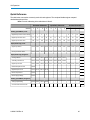
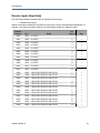
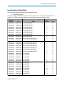
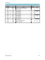
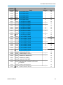
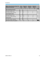
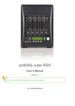
1
I/O Expansion
Serial Bases:
IOE-4404
IOE-4422
IOE-4440
Expansion Modules:
IOEX-4404
IOEX-4422
IOEX-4440
Covering Firmware 2.2.0
User Manual and Reference Guide
Part Number: LUM0017AB
Revision: A
Last Updated: 01/23/2012
Safety Information
The products described in this manual can fail in a variety of modes due to misuse, age, or malfunction. Systems
with these products must be designed to prevent personal injury and property damage during product operation
and in the event of product failure.
Warning! Do not remove or insert diagnostics cable while circuit is live unless the area is
known to be free of ignition concentrations of flammable gases or vapors.
Warranty
FreeWave Technologies, Inc. warrants your FreeWave® Wireless Data Transceiver against defects in materials
and manufacturing for a period of two years from the date of shipment. In the event of a Product failure due to
materials or workmanship, FreeWave will, at its option, repair or replace the Product. The Product must be returned
to FreeWave upon receiving a Return Material Authorization (RMA) for evaluation of Warranty Coverage.
In no event will FreeWave Technologies, Inc., its suppliers, and its licensors be liable for any damages arising from
the use of or inability to use this Product. This includes business interruption, loss of business information, or other
loss which may arise from the use of this Product. Please be advised that OEM customer’s warranty periods may
vary.
Warranty Policy may not apply:
1. If Product repair, adjustments or parts replacements is required due to accident, neglect, unusual
physical, electrical or electromagnetic stress.
2. If Product is used outside of FreeWave specifications.
3. If Product has been modified, repaired, or altered by Customer unless FreeWave specifically
authorized such alterations in each instance in writing. This includes the addition of conformal coating.
Special Rate Replacement Option
A special rate replacement option is offered to non-warranty returns or upgrades. The option to purchase the
replacement unit at this special rate is only valid for that RMA. The special replacement rate option expires if not
exercised within 30 days of final disposition of RMA.
Restricted Rights
Any product names mentioned in this manual may be trademarks or registered trademarks of their respective
companies and are hereby acknowledged. Information in this manual is subject to change without notice and is
proprietary and confidential to FreeWave Technologies, Inc..
This manual is for use by purchasers and other authorized users of FreeWave® transceivers.
No part of this manual may be reproduced or transmitted in any form or by any means, electronic or mechanical, or
for any purpose without the express written permission of FreeWave Technologies, Inc.. FreeWave reserves the
right to make changes to this manual without notice. Unless otherwise agreed to in writing, FreeWave assumes no
responsibility or liability for the use of this manual or the infringement of any copyright or other proprietary
right. FreeWave shall deem nothing contained in this manual as warranty or guarantee.
FreeWave's Wireless Data Transceivers are designed and manufactured in the United States of America.
FreeWave Technologies, Inc.
1800 South Flatiron Court
Boulder, CO 80301
303.381.9200
Toll Free: 1.866.923.6168
Printed in the United States of America.
Copyright © 2012 by FreeWave Technologies, Inc. All rights reserved.
LUM0017AB Rev A
Fax: 303.786.9948
www.freewave.com
ii
This product is licensed by The United States. Diversion contrary to U.S. law is prohibited. Export or re-export
of this product outside of The United States may require authorization by the U.S. Bureau of Industry and
Security. Please contact FreeWave Technologies, Inc. for assistance and further information.
UL Notifications
Models IOE-4404, IOE-4422, IOE-4440, IOEX-4404, IOEX-4422, and IOEX-4440 are suitable for use in Class1,
Division 2, Groups A, B, C, and D or non-hazardous locations only.
The connectors shall not be connected or disconnected while circuit is live unless area is known to be nonhazardous.
Warning! Explosion Hazard - Substitution of any component may impair suitability for Class
1, Division 2.
Warning! Do not remove or insert the diagnostics cable while the circuit is live unless the
area is known to be free of ignition concentrations or flammable gases and vaports.
Input voltage for the IOE and IOEX models is +7.5 to +30 VDC.
Subject Devices are to be installed in the vertical orientation only. Devices were tested for vertical orientation
only and not the horizontal orientation.
Important: Input power and all I/O power, except relay output contacts, shall be
derived from a single Class 2 power source, or equivalent.
LUM0017AB Rev A
iii
FCC Notifications
This device complies with part 15 of the FCC rules. Operation is subject to the following two conditions: 1) This
device may not cause harmful interference and 2) this device must accept any interference received, including
interference that may cause undesired operation.
This device must be operated as supplied by FreeWave Technologies, Inc.. Any changes or modifications made to
the device without the express written approval of FreeWave Technologies, Inc. may void the user's authority to
operate the device.
Note: Whenever any FCC approved FreeWave Technologies, Inc. module is placed inside an
enclosure a label must be placed on the outside of that enclosure which includes the module's
FCC ID.
IC Notifications
This device complies with Industry Canada licence-exempt RSS standard(s). Operation is subject to the following
two conditions: (1) this device may not cause interference, and (2) this device must accept any interference,
including interference that may cause undesired operation of the device.
Ce dispositif est conforme aux normes permis-exemptes du Canada RSS d'industrie. L'opération est sujette aux
deux conditions suivantes : (1) ce dispositif peut ne pas causer l'interférence, et (2) ce dispositif doit accepter
n'importe quelle interférence, y compris l'interférence qui peut causer le fonctionnement peu désiré du dispositif.
LUM0017AB Rev A
iv
Document Revision History
Date
Rev Letter
01/23/2012
A
Updates Made
Updated content to reflect firmware version 2.2.0:
l
The 40000 to 40003: AO Command register description on page 54
has been updated to reflect the maximum output cap of 22 mA.
l
The firmware appendix beginning on page 65 has been updated to
reflect 2.2.0 changes.
The organization and layout of the manual have been updated:
LUM0017AB Rev A
l
Added a Preface which includes general information about this
manual's contents, notational conventions used throughout, how to
contact FreeWave Technical Support, and how to send feedback to
FreeWave about this document.
l
Added information about Serial Base and Expansion Module LEDs.
See "I/O Device LEDs" on page 5.
l
Updated channel descriptions to include detail about applicable Tool
Suite fields and register settings that apply to each. See Chapter 2:
"Channel Functions and Specifications."
l
Added a Glossary that begins on page 67.
v
LUM0017AB Rev A
vi
Table Of Contents
Chapter 1: Introduction
1
About Base Modules and Expansion Modules
1
Serial Base Connectors
2
Serial Base Data Connector
2
Serial Base 485/Power Connector
3
Serial Base Diagnostics Connector
4
Expansion Module Connectors
4
Expansion Module Data Connector
5
Expansion Module Diagnostics Connector
5
I/O Device LEDs
5
Serial Base LEDs
6
Expansion Module LEDs
6
Powering Serial Bases and Expansion Modules
Chapter 2: Channel Functions and Specifications
7
9
IOE-4440 and IOEX-4440 Channels
9
IOE-4422 and IOEX-4422 Channels
10
IOE-4404 and IOEX-4404 Channels
10
Universal Channels
11
Universal Channel as Digital Input
11
Universal Channel as Digital Output
13
Universal Channel as Analog Input
15
Universal Channel as Analog Output
18
Universal Channel as Sensor Power
20
Input-Only Channels
21
Input-Only Channel as Digital Input
21
Input-Only Channel as Analog Input
23
Isolated Channels
27
Isolated Channel as Digital Output
27
Isolated Channel as Digital Input
29
Chapter 3: Setting Up and Programming Serial Bases and Expansion Modules
33
Reading Serial Bases and Expansion Modules in Tool Suite
33
Defining Channel Settings in Tool Suite
34
Upgrading Serial Bases and Expansion Modules to the Latest Firmware
35
Programming Stack Settings in Tool Suite
36
LUM0017AB Rev A
vii
Settings That Apply to the Entire Stack
Chapter 4: Modbus Register Map
37
39
Quick Reference
40
Holding Coils (Read/Write)
41
Discrete Inputs (Read-Only)
44
Input Registers (Read-Only)
45
Holding Registers (Read/Write)
47
Modbus Register Descriptions
50
Holding Coils (Read/Write)
50
0 to 11: DO, Sensor Power ON
50
24 to 35: Apply Default DO, AO, Sensor Power
50
48 to 59: Default DO, Sensor Power State
50
72 to 83: DI Counter Clear
51
92 to 95: High–Speed DI Counter on Isolated
51
96 to 106: DI Counter Falling Edge Increment
51
112 to 119: AI Signed Integer Result
51
120 to 127: AI, AO Current, Voltage Mode
51
136 to 147: DI Counter Latch
52
152 to 163: Pulse Counter De-Bounce
52
Discrete Inputs (Read-Only)
52
10000 to 10011: DI State
52
10024 to 10035: Circuitry Protection Active
52
Input Registers (Read-Only)
52
30000 to 30016: AI Integer Result
52
30032 to 30047: AI Result, Floating Point
53
30064 to 30087: DI Counter
53
30096: Modbus Request Counter
53
30112 to 30119: DO Current
53
30152: Device Temperature
53
30153: VBATT
54
Holding Registers (Read/Write)
54
40000 to 40003: AO Command
54
40008 to 40011: Default AO Command
54
40016 to 40027: Channel Mode
54
40040 to 40047: AI Filter Setting
54
40056 to 40063: Resistor Pull Setting
55
LUM0017AB Rev A
viii
40072 to 40075: AO Resolution
55
40080 to 40091: DO Monostable Timeout
55
40096 to 40103: AI Zero Voltage
55
40104 to 40111: AI Voltage Span
55
40112 to 40119: AI, AO Zero Current
56
40120 to 40127: AI, AO Current Span
56
40128: Comm Connection
57
40129: Comm Timeout Latch
57
40130: Comm Port Baud Rate
58
40131: Comm Port Parity
58
40132: Comm Port Stop Bits
58
40133: Modbus Min Transmit Inter-Message Interval
58
40134: RS-485 Turn-On Delay
58
40135: RS-485 Turn-Off Delay
58
Modbus Timing
Chapter 5: Additional I/O Expansion Information
59
61
Serial Base Dimensions
62
Expansion Module Dimensions
63
Physical Specifications
64
Appendix A: Firmware updates
65
Version 2.2.0
65
Version 2.1.0
66
Glossary
67
Index
69
LUM0017AB Rev A
ix
LUM0017AB Rev A
x
Preface
This document includes the following regarding the FreeWave I/O Expansion products:
l
A basic introduction to the Serial Bases and Expansion Modules that make up the I/O product line.
l
Descriptions of each port and LED on Serial Bases and Expansion Modules.
l
A description of the parameters required for each channel.
l
Steps to setting up and programming a stack of Expansion Modules using Tool Suite.
l
Pin out and mechanical drawings.
l
Modbus register map details.
For information about the firmware releases that apply to the I/O Expansion products, see Appendix A.
Notational Conventions
This guide uses the following notational conventions:
l
l
l
Bold - Indicates items that you select, parameter settings, and parameter names.
Warning! - Indicates a situation that might cause damage to your radio, data, or network.
- Provides time saving or informative suggestions about using the product.
The term "radio" and "transceiver" are used throughout this manual to refer to the described devices.
Contacting FreeWave Technical Support
For up-to-date troubleshooting information, check the Support page at www.freewave.com.
LUM0017AB Rev A
xi
I/O Expansion
FreeWave provides technical support Monday through Friday, 7:30 AM to 5:30 PM Mountain Time (GMT -7).
Call toll-free at 1.866.923.6168, within Colorado call 303.381.9200, or contact us through email at
[email protected].
Documentation Feedback
Your feedback is important to us! FreeWave Technologies, Inc. is committed to continually improving the
quality of our documentation. If you have any comments or suggestions about this document, send them to us
at [email protected]. Please include the title of the document or the document's part number in your
email.
LUM0017AB Rev A
xii
Chapter 1: Introduction
The I/O Expansion product family provides expandable digital input, digital output, analog input, and analog
output capabilities for any device with a Modbus controller. Expandable I/O can be added directly to PLCs,
RTUs, and SCADA hosts. I/O Expansion can also integrate into new and existing wireless communication
systems such as proprietary, licensed and unlicensed, cellular and satellite radio systems.
The I/O Expansion Module may either be stacked on an applicable I/O base or can serve as expandable I/O
modules through a serial connection. Regardless of the configuration, up to 15 modules can be stacked on a
single Radio Base or Serial Base, providing up to 192 I/O points, including those on the Base Module.
About Base Modules and Expansion Modules
The bottom unit in a stack of I/O Expansion Modules is referred to as the Base Module and provides
communication to the outside world. The Base Module in a stack can be one of the following:
LUM0017AB Rev A
1
I/O Expansion
l
Radio Base - A Radio Base provides expandable, wireless I/O and can be polled and controlled
wirelessly across FreeWave's wireless serial network. The FGR2-IO-IOE radio is the only Radio
Base device available. The photo of an I/O Expansion stack on previous page shows an FGR2-IOIOE as the Base Module. For information about the FGR2-IO-IOE, see the Wire Replacement I/O
User Manual (part number LUM0008AC) This document does not provide reference information for
the FGR2-IO-IOE.
l
Serial Base - A Serial Base provides expandable, wired I/O to any device with RS232, RS422,
and RS484 data communication interfaces. Serial Bases come in the following models:
l
IOE-4404
l
IOE-4422
l
IOE-4440
Expansion Modules can be added to a Radio Base or Serial Base device to expand the number of I/O
channels available. Expansion Modules on their own do not communicate. They must be connected to a
Radio Base or a Serial Base. The following expansion modules are available. The "X" in the model number
indicates that the model is an expansion module.
l
IOEX-4404
l
IOEX-4422
l
IOEX-4440
Different isolated channels are available depending on the model number. For more information, see "Channel
Functions and Specifications" on page 9.
Serial Base Connectors
The following sections describe each connector on a Serial Base and the pin layout of each. For information
about the I/O channels available on the Serial Base, see "Channel Functions and Specifications" on page 9.
Serial Base Data Connector
This 10-pin connector provides serial communication and power to the Serial Base and supports RS232,
RS422, and RS485 serial communication interfaces.
LUM0017AB Rev A
2
User Manual and Reference Guide
When Expansion Modules are connected to the Serial Base, power is provided to the Expansion Modules
through the power and ground pins on this connector. If the Expansion Modules have a Serial Base, power can
alternatively be supplied by the serial 485/Power Connector described in "Serial Base 485/Power Connector"
on page 3.
The following pin-out summarizes the function of each pin in the 10-pin data connector:
1.
VBAT
Power
2.
Interrupt
Interrupt used to place the Base into Setup Mode
3.
DTR
Data Terminal Ready
4.
Ground
Ground
5.
TXD
Transmit Data
6.
Ground
Ground
7.
RXD
Receive Data
8.
DCD
Carrier Detect
9.
RTS
Request to Send
10.
CTS
Clear to Send
Pin 1 is the closest pin to the edge of device:
Serial Base 485/Power Connector
This 4-pin connector provides serial communication and power to the Serial Base and any attached Expansion
Modules. The serial communication interface is limited to two-wire 485 when a shorting connector is placed on
the 10-pin connector on top of the device. The shorting connector shorts pins 5 (TXD) to 7 (RXD) for Bus +
and pins 9 (RTS) and 10 (CTS) for Bus -.
The following pin-out summarizes the function of each pin:
B
Bus – for two-wire 485 half duplex with shorting connector
A
Bus + for two-wire 485 half duplex with shorting connector
VBAT
Power
Ground
Ground
LUM0017AB Rev A
3
I/O Expansion
The pins are in the following orientation:
Serial Base Diagnostics Connector
This 20-pin connector provides configuration access to the Serial Base with the Tool Suite configuration
software without removing either the Data Connector or 485/Power connector.
The 20-pin connector on an attached Expansion Module passes diagnostic data and settings directly to and
from the base module (Serial Base or Radio Base).
Expansion Module Connectors
The following sections describe each connector on an I/O Expansion Module. For information about the I/O
channels available on the Expansion Modules, see "Channel Functions and Specifications" on page 9.
LUM0017AB Rev A
4
User Manual and Reference Guide
Expansion Module Data Connector
The 10-pin data connector passes data directly through to the Serial Base or Radio Base. For more
information, see "Serial Base Data Connector" on page 2 or the documentation for the Radio Base for detailed
descriptions.
The data connector on the top Expansion Module can be used to provide power to all devices in the stack.
Connecting power to the 10-pin data connector on the top module delivers the supply voltage to all modules in
the stack. The following pin-out summarizes the function of each pin:
1.
VBAT
Power
2.
Interrupt
Interrupt used to place the Base into Setup Mode
3.
DTR
Data Terminal Ready input of Serial Base
4.
Ground
Ground
5.
TXD
Transmit data output of the Serial Base or Radio Base. Y+ data of RS485 output.
6.
Ground
Ground
7.
RXD
Receive data input of the Serial Base or Radio Base. A+ data of RS485 input.
8.
DCD
Carrier Detect output of Radio Base
9.
RTS
B- data of RS485 input
10.
CTS
Z- data of RS485 input
Expansion Module Diagnostics Connector
The 20-pin diagnostic connector provides board-to-board communication for stacked Expansion Modules. It
also provides access to the diagnostic connector on the base device, whether a Serial Base or Radio Base.
I/O Device LEDs
The LEDs on the Serial Base and Expansion Modules in a stack help identify the state of the system and the
current action happening with each device in the stack:
l
Power - Labeled with a P in enclosed Serial Bases and Expansion Modules, this is the LED
closest to the edge of the device.
l
Inbound - Labeled with an I in enclosed Serial Bases and Expansion Modules, this is the middle
LED.
l
Outbound - Labeled with an O in enclosed Serial Bases and Expansion Modules, this is the LED
closest to the I/O channels.
The LEDs are either red or green, solid, flashing intermittently, or blinking. The state of each LED is described
in the sections below.
Warning! If all the LEDs are solid red or blinking red the device is receiving a firmware
upgrade. Do not unplug the device or remove the device's power during a firmware
upgrade. The device could become inoperable.
LUM0017AB Rev A
5
I/O Expansion
Serial Base LEDs
Serial Base Module
LED State
Power (P)
Solid green
Power on
Intermittent green
flash
Low power mode
Blinking green
Communication reset mode,
device is gathering startup settings
Solid red
Firmware upgrade initiated*
Intermittent red flash
-
Inbound (I)
Outbound (O)
-
-
Receiving a message from the
rest of the stack
-
Device is sending data after being
polled
Device is sending data when polled
1) When the other LEDs are also
solid red a firmware upgrade has
been initiated
1) When the other LEDs are also
solid red a firmware upgrade has
been initiated
1) If other LEDs are also
intermittently flashing red, internal
checks after firmware upgrade
If other LEDs are also intermittently
flashing red, internal checks after
firmware upgrade
2) Device is being polled
Blinking red
Internal checks after firmware
upgrade
Internal checks after firmware
upgrade
Sending information to devices in
the stack
* The Incoming and Outgoing LEDs may appear to blink depending on how many registers are read during a single
polling cycle.
Expansion Module LEDs
Expansion Module
Inbound (I)
Outbound (O)
Solid green
LED State
Power on
Power (P)
-
-
Intermittent green
flash
Low power mode
-
Sending information down the stack
to the base
Communication reset mode,
device is gathering startup
settings
-
-
Blinking green
*
Solid red
Firmware upgrade initiated*
Intermittent red
flash
Blinking red
-
*
Internal checks after firmware
upgrade
1) When the other LEDs are also
solid red a firmware upgrade has
been initiated
1) When the other LEDs are also
solid red a firmware upgrade has
been initiated
2) Receiving a command from the
base
2) Receiving a command from the
base
Device is being polled
Internal checks after firmware
upgrade
-
Sending information to devices in
the stack
* The Incoming and Outgoing LEDs may appear to blink depending on how many registers are read during a single
polling cycle.
LUM0017AB Rev A
6
User Manual and Reference Guide
Powering Serial Bases and Expansion Modules
Power is shared between all devices in a stack of Expansion Modules. When one device in the stack is
powered (Expansion Module, Serial Base, or Radio Base) then all connected devices are powered.
A stack of Expansion Modules can be powered through one of the following:
l
Data Connector on the top Expansion Module. See "Expansion Module Data Connector" on page
5.
l
485/Power Connector on a Serial Base. See "Serial Base 485/Power Connector" on page 3.
l
I/O Connector on a Radio Base. See the Wire Replacement I/O User Manual (part number
LUM0008AC) for details about powering the FGR2-IO-IOE.
Power supply voltage limits for all Serial Base and Expansion Modules are as follows:
Item
Power Supply Voltage
Min
Typical
Max
Units
7.5
-
30
V
The following table provides the current consumption for a sample Serial Base and Expansion Module
configuration as follows:
Current Consumption
at 12 V (in mA)
Channel Configuration
Universal
Channels
Input-Only
Channels
Isolated
Channels
12 V
Disabled
Disabled
Disabled
17.0
DO: Off
Disabled
DO: Off
17.0
DO: On
Disabled
DO: On
18.1
DI
DI
DI
17.0
AO: 0 mA
Disabled
Disabled
18.2
AO: 20 mA
Disabled
Disabled
98.2
AI: Voltage
AI: Voltage
Disabled
17.0
AI: Current
AI:Current
Disabled
25.0
LUM0017AB Rev A
7
LUM0017AB Rev A
8
Chapter 2: Channel Functions and
Specifications
All I/O Expansion devices have 12 I/O channels. All models feature four universally configurable channels,
four input-only channels, and four electrically isolated channels.
The different models have the following I/O configuration:
l
IOE-4440 and IOEX-4440 - All four isolated channels are digital inputs.
l
IOE-4422 and IOEX-4422 - Two isolated channels are digital inputs and two isolated channels are
digital outputs.
l
IOE-4404 and IOEX-4404 - All four isolated channels are digital outputs.
IOE-4440 and IOEX-4440 Channels
The following channels are available on the IOE-4440 and IOEX-4400 Channels. Any channel column with a
dot ( • ) in the table below is available in this model.
Universal Channels
Input-Only Channels
Isolated Channels
4440 Channels
Number
1
2
3
4
5
6
7
8
9
10
11
12
Digital Input
12
•
•
•
•
•
•
•
•
•
•
•
•
Digital Output
4
•
•
•
•
Analog Input
8
•
•
•
•
•
•
•
•
Analog Output
4
•
•
•
•
Sensor Power
4
•
•
•
•
LUM0017AB Rev A
9
I/O Expansion
IOE-4422 and IOEX-4422 Channels
The following channels are available on the IOE-4422 and IOEX-4422 Channels. Any channel column with a
dot ( • ) in the table below is available in this model.
Universal Channels
Input-Only Channels
Isolated Channels
4422 Channels
Number
1
2
3
4
5
6
7
8
9
10
Digital Input
10
•
•
•
•
•
•
•
•
•
•
Digital Output
6
•
•
•
•
Analog Input
8
•
•
•
•
Analog Output
4
•
•
•
•
Sensor Power
4
•
•
•
•
•
•
•
11
12
•
•
•
IOE-4404 and IOEX-4404 Channels
The following channels are available on the IOE-4404 and IOEX-4404 Channels. Any channel column with a
dot ( • ) in the table below is available in this model.
Universal Channels
Input-Only Channels
4404 Channels
Number
1
2
3
4
5
6
7
8
Digital Input
8
•
•
•
•
•
•
•
•
Digital Output
8
•
•
•
•
Analog Input
8
•
•
•
•
Analog Output
4
•
•
•
•
Sensor Power
4
•
•
•
•
•
•
•
Isolated Channels
9
10
11
12
•
•
•
•
•
The I/O channels are numbered left to right and each as a channel port and a signal ground port:
LUM0017AB Rev A
10
User Manual and Reference Guide
Universal Channels
Channels 1, 2, 3, and 4 on all Serial Base and Expansion Modules are universal channels. Universal channels
can be configured as Digital Input, Digital Output, Analog Input, Analog Output, or Sensor Power channels.
The following sections describe the features and characteristics of each universal channel configuration.
Universal Channel as Digital Input
A universal Digital Input provides data to the following registers:
l
10000 to 10011: DI State - The present state of the channel.
l
30064 to 30087: DI Counter - The number of pulse edges seen on the channel.
You can configure a Digital Input's settings in either Tool Suite or directly through the register settings. For
information about setting a universal channel as a Digital Input, see "Defining Channel Settings in Tool Suite "
on page 34.
LUM0017AB Rev A
11
I/O Expansion
Use the information in the following table to configure a Digital Input.
Field in
Tool Suite
Counter Edge
Register
96 to 106: DI Counter Falling
Edge Increment
Description
Sets the pulse edge on which the
DI Counter register increments.
Select Falling Edgeto increment the
DI Counter register when the input goes
from 1 to 0. In the Modbus register, this is (1)
ON.
Select Rising Edge to increment the
DI Counter register when input goes from 0
to 1. In the Modbus register, this is (0) OFF.
Resistor Pull
40056 to 40063: Resistor Pull
Setting
Select Pull-Down to connect a pull-down
resistor to ground for use with closedcontact-to-voltage inputs. In the Modbus
register, this is 1.
Select Pull-Up to connect a pull-up resistor
for closed-contact-to-ground inputs. In the
Modbus register, this is 2.
Select None to disable both resistors. In the
Modbus register, this is 0.
Set additional functionality for a Digital Input using the following registers that do not have an equivalent field
in Tool Suite:
Register
Description
72 to 83: DI Counter Clear
Clears the Digital Input counter to 0. Critical counting ensures that
each pulse is reported by only clearing pulses that you have read. For
more information, see the DI Counter Clear register description on
page 51.
136 to 147: DI Counter
Latch
Allows you to scan for the input change at a much slower speed than
the duration of the pulse. For more information, see the DI Counter
Latch register description on page 52.
152 to 163: Pulse Counter
De-bounce
Enables the system to take multiple samples before determining that
an edge is real and not noise on the channel. Universal Digital Inputs
support pulse counting for input signals up to 100 Hz; de-bounced
pulse counting for input signals to 10 Hz.
LUM0017AB Rev A
12
User Manual and Reference Guide
A universal channel configured as a Digital Input has the following specifications:
Item
Min
Typical
Max
Units
Input Low (OFF) voltage
0
-
2.5
V
Input High (ON) voltage
3.0
-
Actual Power
Supply Voltage
V
Pulse counting frequency
-
-
100
Hz
De-bounced pulse counting frequency
-
-
10
Hz
Pulse width
4
-
-
ms
De-bounced pulse width
40
-
-
ms
Pull-up resistance
-
1
-
kΩ
Pull-up voltage (measured externally)
-
3.0
-
V
Pull-down resistance to ground
-
10
-
kΩ
Universal Channel as Digital Output
A universal channel configured as a Digital Output has the following characteristics:
l
Solid-state digital outputs with reverse-blocking Schottky diodes are rated at 1 A across the
complete operating temperature range.
l
Output voltage range up to 30 V, or device supply voltage, whichever is less.
l
Circuitry protection. If an overload occurs, the channel turns off automatically. For more
information, see the description for 10024 to 10035: Circuitry Protection Active register on page
52.
l
Each channel has a ground pin for current return that must be used for large currents (over 0.1 A).
l
Reports approximate amount of current flowing to ground.
l
Configurable for normally open or normally closed.
A Digital Output reports its current in milliAmps to the 30112 to 30119: DO Current register.
You can configure a Digital Output's settings in either Tool Suite or directly through the register settings. For
information about setting a universal channel as Digital Output, see "Defining Channel Settings in Tool Suite "
on page 34.
Use the information in the following table to configure a Digital Output.
LUM0017AB Rev A
13
I/O Expansion
Field in
Tool Suite
Register
Apply Default
Output
24 to 35: Apply Default
DO, AO, Sensor Power
Description
If set to Yes, when a device powers up or a
communication timeout has occurred, the channel uses
the values set in the Default DO, Sensor Power State
register. In the Modbus register, this is (1) ON.
If set to Yes, also set the Default Output field or the
Default DO, Sensor Power State register.
If set to No, when a device powers up or a communication
timeout has occurred, the channel remains off. In the
Modbus register, this is (0) OFF.
Default Output
48 to 59: Default DO,
Sensor Power State
If you selected to apply defaults on power up or after a
communication timeout, use this setting to set the default
state of the channel.
Monostable
Time
40080 to 40091: DO
Monostable Timeout
Enter the amount of time in milliseconds from 1 to 60000
(1 minute) after which the Digital Output channel goes to
the state defined in the Default DO, Sensor Power State
register.
When set to 0 milliseconds, the channel is bi-stable and
maintains its most recent state until it receives a
command to change its state.
Set the following field in the Stack Settings tab in Tool Suite for the Serial Base in the stack:
Field
Default Delay
Description
Enter the amount of time in seconds that an Expansion Module or
Serial Base waits for a Modbus command or query before a
communication timeout occurs. When a communication timeout
occurs, the action defined in the Apply Default DO, AO, Sensor
Power is taken. For more information, see the register description on
page 50.
Set additional functionality for a Digital Output using the following registers that do not have an equivalent field
in Tool Suite:
Register
0 to 11: DO, Sensor Power
On
LUM0017AB Rev A
Description
Set to (1) ON to sink current to ground when the transistor powers up.
When set to (0) OFF, the transistor turns off and the output remains
floating, unless the Resistor Pull Setting register is set to 1 or 2.
14
User Manual and Reference Guide
Register
40056 to 40063: Resistor
Pull Setting
Description
Select Pull-Down to connect a pull-down resistor to ground for use
with closed-contact-to-voltage inputs. In the Modbus register, this is
1.
Select Pull-Up to connect a pull-up resistor for closed-contact-toground inputs. In the Modbus register, this is 2.
Select None to disable both resistors. In the Modbus register, this is
0.
A universal channel configured as a Digital Output has the following specifications:
Item
Min
Typical
Max
Units
Output ON sinking current
-
-
1
A
Output ON resistance to ground*
0
0.1
0.2
Ω
Output ON circuitry protection limit
-
1.25
-
A
Output OFF resistance to ground
234
-
-
kΩ
External load voltage connection
0
-
VBAT
V
Pull-up resistance
-
1
-
kΩ
Pull-up voltage (measured externally)
-
3.0
-
V
Pull-down resistance to ground
-
10
-
kΩ
* Dynamic resistance; a reverse-blocking Shottky diode is in series.
Universal Channel as Analog Input
A universal channel configured as an Analog Input returns data to the 30000 to 30016: AI Integer Result
register and 30032 to 30047: AI Floating Point Result register associated with the channel. The channel
also has circuitry protection. If an overload occurs, the channel turns off automatically. For more information,
see the description for 10024 to 10035: Circuitry Protection Active register on page 52.
You can configure an Analog Input's settings in either Tool Suite or directly through the register settings.
For information about setting a universal channel as an Analog Input, see "Defining Channel Settings in Tool
Suite " on page 34.
Use the information in the following table to configure an Analog Input.
LUM0017AB Rev A
15
I/O Expansion
Field in
Tool Suite
Voltage Or
Current
Equivalent Register
120 to 127: AI Current
Mode
Description
Select Voltage to return information in Volts (V).
In the Modbus register, this is (1) ON.
Select Current to return current information in
milliAmps (mA). In the Modbus register, this is
(0) OFF.
Offset/Zero
40112 to 40119 AI, AO Zero
Current
40096 to 40103: AI Zero
Voltage
Span
40104 to 40111: AI Voltage
Span
40120 to 40127: 40 AI, AO
Current Span
l
20-bit analog-to-digital converter yields 0.10%
reading accuracy across entire operating
temperature for voltage and current input
signals.
l
Voltage range supports 1 to 5 V and 0 to 10 V
analog signals. Complete voltage range is -2.5
to 12.5 V.
l
Current range supports 4 to 20 mA analog
signals. Complete current range is 0 to 25 mA.
Calibrates the low end of the Analog Input to
zero. Set between 0 to 10000 mV or mA depending on your setting in the Voltage Or Current
field.
Sets the high end, or range, of the Analog Input.
See the AI, AO Current Span register
description on page 54 for setting
recommendations.
For 16-bit readings, set between 0 and 65535.
For 20-bit readings, set between 0 and
1,048,575.
Filtering/
Averaging
LUM0017AB Rev A
40040 to 40027: AI Filter
Setting
Sets a moving average, in seconds, for the AI
Integer Result and AI Floating Point Result
registers. You can use this setting to help filter
out signal noise if in a noisy environment.
FreeWave recommends leaving this setting at 0.
Select from the following settings:
l
0 - Disabled
l
1 - 10 seconds (0.1 Hz)
l
2 - 25 seconds (0.04 Hz)
l
3 - 50 seconds (0.02 Hz)
l
4 - 100 seconds (0.01 Hz)
l
5 - 250 seconds (0.004 Hz)
16
User Manual and Reference Guide
Field in
Tool Suite
Resistor Pull
Equivalent Register
Description
40056 to 40063: Resistor
Pull Setting
Select Pull-Down to connect a pull-down
resistor to ground for use with closed-contact-tovoltage inputs. In the Modbus register, this is 1.
Select Pull-Up to connect a pull-up resistor for
closed-contact-to-ground inputs. In the Modbus
register, this is 2.
Select None to disable both resistors. In the
Modbus register, this is 0.
Integer Type
112 to 119: AI Signed
Integer Result
Sets the integer type to a signed or unsigned
integer in the AI Integer Result register. A
signed integer is required to report negative input
voltages or if the RTU/PLC supports signed
integers only.
Setting this register to 0 results in an unsigned
integer returned in the AI Integer Result register.
Setting to 1 results in a signed integer.
Set the following fields in the Stack Settings tab in Tool Suite for the Serial Base:
Field
Description
Floating Point Word Order
Determines the position of the Most Significant Word (MSW) and
Lease Significant Word (LSW) in the AI Floating Point Result
register for all devices in the stack. Regular word order places the
MSW at the lower address and the LSW at the higher address. For
example MSW = 30032, LSW = 30033. Inverted word order places the
LSW at the lower address and the MSW at the higher address. For
example LSW = 30032, MSW = 30033).
AI Integer Results
Justification
Determines the alignment of the AI Integer Result register. Options
include Left and Right.
A universal channel configured as an Analog Input has the following specifications:
Item
Min
Typical
Max
Units
Voltage Input
Analog input voltage
-2.5
-
lesser of 30 V or VBAT
V
Full-scale input voltage*
-
13.75
-
V
Resolution*
-
20
-
Bits
Scaling factor (all 20 bits)*
-
9.54
-
μV/LSB
LUM0017AB Rev A
17
I/O Expansion
Item
Min
Typical
Max
Units
Scaling factor (upper 16 bits)*
-
153
-
μV/LSB
Accuracy error (0 to 5 V input)
0
-
Greater of 1 mV or 0.10% of input
mA
Analog input current
0
-
25
mA
Circuitry protection limit
-
25
-
mA
Internal sense resistor
249
250
251
Ω
Full-scale input current range*
-
40
-
mA
Resolution
-
20
-
Bits
Scaling factor (all 20 bits)*
-
38.1
-
nA/LSB
Scaling factor (upper 16 bits)*
-
610
-
na/LSB
Accuracy error (4 to 20 mA input)
0
-
Greater of 4 μA or 0.10% of input
Current Input
*These settings apply only when zero and span registers are set to 0 (default)
Universal Channel as Analog Output
You can configure a Analog Output's settings in either Tool Suite or directly through the register settings. For
information about setting a universal channel as an Analog Output, see "Defining Channel Settings in Tool
Suite " on page 34.
Use the information in the following table to configure an Analog Output.
Field in
Tool Suite
Scaling
Register
40072 to 40075:
AO Resolution
Description
Sets the resolution of the AO Command register. Set
to one of the following options:
l
microAmps (1 microAmp per bit)
l
16-bit resolution
l
15-bit resolution. This is the recommended setting
PLCs or RTUs that only support 16-bit signed
integers.
l
14- bit resolution
l
12-bit resolution
Current range supports 4 to 20 mA analog signals.
Complete current range is 0 to 25 mA.
LUM0017AB Rev A
18
User Manual and Reference Guide
Field in
Tool Suite
Register
Apply Default
Output
Description
24 to 35: Apply Default
DO, AO, Sensor Power
If set to Yes, when a device powers up or a
communication timeout has occurred, the channel
uses the values set in the AO Command register. In
the Modbus register, this is (1) ON.
If set to Yes, also set the Default Output field or the
Default AO Command register.
If set to No, when a device powers up or a
communication timeout has occurred, the factory
defaults are applied to the channel. In the Modbus
register, this is (0) OFF.
Default Output
40008 to 40011: Default
AO Command
If you selected to apply defaults on power up or after a
communication timeout, use this setting to set the
default state of the channel.
Offset/Zero
40112 to 40119: AI, AO
Zero Current
Calibrates the low end of the Analog Output to zero.
Set between 0 to 10000 mV or mA depending on your
setting in the Voltage Or Current field.
Span
40112 to 40119: AI, AO
Zero Current
Sets the high end, or range, of the Analog Output. See
the AI, AO Current Span register description on
page 56for setting recommendations.
40120 to 40127: AI, AO
Current Span
For 16-bit readings, set between 0 and 65535.
For 20-bit readings, set between 0 and 1,048,575.
Resistor Pull
40056 to 40063: Resistor
Pull Setting
Select Pull-Down to connect a pull-down resistor to
ground for use with closed-contact-to-voltage inputs.
In the Modbus register, this is 1.
Select Pull-Up to connect a pull-up resistor for
closed-contact-to-ground inputs. In the Modbus
register, this is 2.
Select None to disable both resistors. In the Modbus
register, this is 0.
A universal channel configured as a Analog Output has the following specifications:
Item
Min
Typical
Max
Units
Analog output current
0
-
22
mA
Full-scale output current*
-
25
-
mA
Resolution
-
25
-
Bits
Scaling factor*
-
1
-
μA/LSB
Voltage on output pin
-
-
VBAT -0.5
V
LUM0017AB Rev A
19
I/O Expansion
Item
Min
Accuracy error (at 20 mA output)
Typical
-0.25
Max
-
Units
0.25
%
* These settings apply only when the zero and range registers are set to 0 (default).
Universal Channel as Sensor Power
A universal channel configured as a Sensor Power channel provides the following:
l
Power for sensors and transmitters up to 50 mA.
l
Voltage provided to the transmitter is roughly equal to the power provided to the Serial Base or
Expansion Module, minus approximately 0.5 V, minus load current, multiplied by 10 ohms.
l
Circuitry protection. If an overload occurs, the channel turns off automatically. For more
information, see the description for 10024 to 10035: Circuitry Protection Active register on page
52.
You can configure a Sensor Power channel's settings in either Tool Suite or directly through the register
settings. For information about setting a universal channel as a Sensor Power channel, see "Defining Channel
Settings in Tool Suite " on page 34
Use the information in the following table to configure a Sensor Power channel.
Field in
Tool Suite
Register
Apply Default
Output
Description
24 to 35: Apply Default DO,
AO, Sensor Power
If set to Yes, when a device powers up or a
communication timeout has occurred, the
channel uses the values set in the DO, Sensor
Power On register. In the Modbus register, this
is (1) ON.
If set to Yes, also set the Default Output field
or the Default DO, Sensor Power register.
If set to No, when a device powers up or a
communication timeout has occurred, the
factory defaults are applied to the channel. In
the Modbus register, this is (0) OFF.
Default Output
48 to 59: Default DO,
Sensor Power State
If you selected to apply defaults on power up or
after a communication timeout, use this setting
to set the default state of the channel.
A universal channel configured as Sensor Power has the following characteristics:
Item
Min
Typical
Max
Units
Voltage output
VBAT - 1
VBAT - 0.5
VBAT
V
Current output
0
-
50
mA
Circuitry protection limit
-
52
-
mA
LUM0017AB Rev A
20
User Manual and Reference Guide
Input-Only Channels
Channels 5, 6, 7, and 8 on all Serial Bases and Expansion Modules are input-only channels. Input-only
channels can be configured as Digital Input and Analog Input.
The following sections describe the features and characteristics of each input-only channel configuration.
Input-Only Channel as Digital Input
An input-only channel configured as a Digital Input provides data to the following registers:
l
10000 to 10011: DI State - The present state of the channel.
l
30064 to 30087: DI Counter - The number of pulse edges seen on the channel.
You can configure a Digital Input's settings in either Tool Suite or directly through the register settings. For
information about setting an input-only channel as a Digital Input, see "Defining Channel Settings in Tool Suite
" on page 34.
Use the information in the following table to configure an input-only channel Digital Input.
Field in
Tool Suite
Counter Edge
Register
96 to 106: DI Counter Falling
Edge Increment
Description
Sets the pulse edge on which the
DI Counter register increments.
Select Falling Edge to increment the
DI Counter register when the input goes
from 1 to 0. In the Modbus register, this is (1)
ON.
Select Rising Edge to increment the
DI Counter register when input goes from 0
to 1. In the Modbus register, this is (0) OFF.
LUM0017AB Rev A
21
I/O Expansion
Field in
Tool Suite
Counting Speed
Register
Description
92 to 95: High-Speed DI Counter
on Isolated
Determines which channels use pulse
counting for input signals up to 10 kHz. If you
set an input-only channel to be high-speed,
its corresponding isolated channel is set to
standard speed. For more information, see
the High-Speed DI Counter on Isolated
register description on page 51
Select Fast to set the channel to high-speed.
In the Modbus register, this is (1) ON.You
can assign high-speed counting to only one
channel of 5 or 9, 6 or 10, 7 or 11, and 8 or 12.
Note: High-speed counting is not debounced and inputs must not go below GND.
Select Slow to set the channel to standardspeed. Standard speed counters support 100
Hz pulses, or 10 Hz pulses with de-bounce.
In the Modbus register, this is (0) OFF.
Resistor Pull
40056 to 40063: Resistor Pull
Setting
Select Pull-Down to connect a pull-down
resistor to ground for use with closedcontact-to-voltage inputs. In the Modbus
register, this is 1.
Select Pull-Up to connect a pull-up resistor
for closed-contact-to-ground inputs. In the
Modbus register, this is 2.
Select None to disable both resistors. In the
Modbus register, this is 0.
Important: For accurate counting at high speed, the voltage at the Digital Input pin
must not drop below 0 V. Proper grounding techniques and short wiring connections
are necessary to ensure accurate counting for high speed signals. If the voltage at the
Digital Input pin drops below 0 V, there may be false edges detected and the Digital
Input pulse count can be higher than expected.
Set additional functionality for a Digital Input using the following registers that do not have an equivalent field
in Tool Suite:
Register
72 to 83: DI Counter Clear
LUM0017AB Rev A
Description
Clears the Digital Input counter to 0. Critical counting ensures that
each pulse is reported by only clearing pulses that you have read. For
more information, see the DI Counter Clear register description on
page 51.
22
User Manual and Reference Guide
Register
Description
136 to 147: DI Counter
Latch
Allows you to scan for the input change at a much slower speed than
the duration of the pulse. For more information, see the DI Counter
Latch register description on page 52.
152 to 163: Pulse Counter
De-bounce
Enables the system to take multiple samples before determining that
an edge is real and not noise on the channel. Digital Inputs support
pulse counting for input signals up to 100 Hz; de-bounced pulse
counting for input signals to 10 Hz.
Note: High-speed counting is not de-bounced and inputs must not go
below GND.
An input-only channel configured as a Digital Input has the following specifications:
Item
Min
Typical
Max
Units
Input low (OFF) voltage
0
-
2.5
V
Input high (ON) voltage
3.0
-
VDD
V
Pulse counting frequency, standard speed
-
-
100
Hz
Pulse counting frequency, high speed
-
-
10
kHz
Pulse counting frequency, de-bounced pulse
-
-
10
Hz
Pulse width, standard speed
4
-
-
ms
Pulse width, high-speed
40
-
-
μs
Pulse width, de-bounced
40
-
-
ms
Pull-up resistance
-
1
-
kΩ
Pull-up voltage (measured externally)
-
3.0
-
V
Pull-down resistance to ground
-
10
-
kΩ
Input-Only Channel as Analog Input
An input-only channel configured as an Analog Input returns data to the 3000 to 30016: AI Integer Result
register and 30032 to 30047: AI Floating Point Result register associated with the channel. The channel
also has circuitry protection. If an overload occurs, the channel turns off automatically. For more information,
see the description for 10024 to 10035: Circuitry Protection Active register on page 52.
You can configure an Analog Input's settings in either Tool Suite or directly through the register settings. For
information about setting an input-only channel as an Analog Input, see "Defining Channel Settings in Tool
Suite " on page 34.
Use the information in the following table to configure an Analog Input.
LUM0017AB Rev A
23
I/O Expansion
Field in
Tool Suite
Voltage Or
Current
Equivalent Register
120 to 127: AI Current Mode
Description
Select Voltage to return information in
Volts (V). In the Modbus register, this is (1)
ON.
Select Current to return current
information in milliAmps (mA). In the
Modbus register, this is (0) OFF.
Offset/Zero
40112 to 40119: AI, AO Zero
Current
40096 to 40103: AI Zero Voltage
Span
40104 to 40111: AI Voltage Span
40120 to 40127: AI, AO Current
Span
l
20-bit analog-to-digital converter yields
0.10% reading accuracy across entire
operating temperature for voltage and
current input signals.
l
Voltage range supports 1 to 5 V and 0 to
10 V analog signals. Complete voltage
range is -2.5 to 12.5 V.
l
Current range supports 4 to 20 mA
analog signals. Complete current range
is 0 to 25 mA.
Calibrates the low end of the Analog Input
to zero. Set between 0 to 10000 mV or mA
depending on your setting in the Voltage
Or Current field.
Sets the high end, or range, of the Analog
Input. See the AI, AO Current Span
register description on page 56 for setting
recommendations.
For 16-bit readings, set between 0 and
65535.
For 20-bit readings, set between 0 and
1,048,575.
Filtering/
Averaging
LUM0017AB Rev A
40040 to 40047: AI Filter Setting
Sets a moving average, in seconds, for the
AI Integer Result and AI Floating Point
Result registers. Use this setting to help
filter out signal noise. Select from the
following settings:
l
0 - Disabled
l
1 - 10 seconds
l
2 - 25 seconds
l
3 - 50 seconds
l
4 - 100 seconds
l
5 - 250 seconds
24
User Manual and Reference Guide
Field in
Tool Suite
Resistor Pull
Equivalent Register
Description
40056 to 40063: Resistor Pull Set- Select Pull-Down to connect a pull-down
ting
resistor to ground for use with closedcontact-to-voltage inputs. In the Modbus
register, this is 1.
Select Pull-Up to connect a pull-up
resistor for closed-contact-to-ground
inputs. In the Modbus register, this is 2.
Select None to disable both resistors. In
the Modbus register, this is 0.
Integer Type
112 to 119: AI Signed Integer
Result
Sets the integer type to a signed or
unsigned integer in theAI Integer Result
register. A signed integer is required to
report negative input voltages if the
RTU/PLC supports signed integers only.
Setting to Signed results in a signed
integer. In the Modbus register, this is (1)
ON.
Setting to Unsigned results in an
unsigned integer returned in the AI Integer
Result register. In the Modbus register,
this is (0) OFF.
Set the following parameters in the Stack Settings tab in Tool Suite for the Serial Base:
Field
Description
Floating Point Word Order
Determines the position of the Most Significant Word (MSW) and
Lease Significant Word (LSW) in the AI Floating Point Result
register for all devices in the stack. Regular word order places the
MSW at the lower address and the LSW at the higher address. For
example MSW = 30032, LSW = 30033. Inverted word order places the
LSW at the lower address and the MSW at the higher address. For
example LSW = 30032, MSW = 30033).
AI Integer Results
Justification
Determines the alignment of the AI Integer Result register. Options
include Left and Right.
An input-only channel configured as a Analog Input has the following specifications:
Item
Min
Typical
Max
Units
Voltage Input
Analog input voltage
LUM0017AB Rev A
-2.5
-
30
V
25
I/O Expansion
Item
Min
Typical
Max
Units
Full-scale input voltage*
-
13.75
-
V
Resolution
-
20
-
Bits
Scaling factor (all 20 bits)*
-
9.54
-
μV/LSB
Scaling factor (upper 16 bits)*
-
153
-
μV/LSB
Accuracy error (0 to 5 V input)
0
-
Greater of 1 mV or 0.10% of input
mA
Analog input current
0
-
25
mA
Circuitry protection limit
-
25
-
mA
Internal sense resistor
249
250
251
Ω
Full-scale input current range*
-
40
-
mA
Resolution
-
20
-
Bits
Scaling factor (all 20 bits)*
-
38.1
-
nA/LSB
Scaling factor (upper 16 bits)*
-
610
-
nA/LSB
Accuracy error (4 to 20 mA input)
0
-
Greater of 4 μA or 0.10% of input
Current Input
*These settings apply only when zero and span registers are set to 0 (default)
LUM0017AB Rev A
26
User Manual and Reference Guide
Isolated Channels
Channels 9, 10, 11, and 12 are built in the factory for either Digital Input or Digital Output. These channels can
only serve the function for which they were built.
The following sections describe the features and characteristics of each isolated channel configuration.
Isolated Channel as Digital Output
An isolated Digital Output reports its current in milliAmps to the DO Current register and also has the
following characteristics:
l
Mechanical relays capable of switching up to 2 A at 250 VDC or VAC
l
Long life relays with 80,000 cycles
l
Configured for normally open
l
Circuitry protection. If an overload occurs, the channel turns off automatically. For more
information, see the description for 10024 to 10035: Circuitry Protection Active register on page
52.
You can configure a Digital Output's settings in either Tool Suite or directly through the register settings.For
information about setting an isolated channel as a Digital Output, see "Defining Channel Settings in Tool Suite
" on page 34.
Use the information in the following table to configure a Digital Output.
LUM0017AB Rev A
27
I/O Expansion
Field in
Tool Suite
Apply Default
Output
Register
24 to 35: Apply Default DO,
AO, Sensor Power
Description
If set to Yes, when a device powers up or a
communication timeout has occurred, the
channel uses the values set in the Default
DO, Sensor Power State register. In the
Modbus register, this is (1) ON.
If set to Yes, also set the Default Output field
or the Default DO, Sensor Power State
register.
If set to No, when a device powers up or a
communication timeout has occurred, the
factory defaults are applied to the channel. In
the Modbus register, this is (0) OFF.
Default Output
48 to 59: Default DO, Sensor
Power State
If you selected to apply defaults on power up or
after a communication timeout, use this setting
to set the default state of the channel. For more
information, see the Default DO, Sensor
Power State register description on page 50.
Monostable Time
40080 to 40091: DO
Monostable Timeout
Enter the amount of time in milliseconds from 1
to 60000 (1 minute) after which the Digital
Output channel goes to the state defined in the
Default DO, Sensor Power State register.
When set to 0 milliseconds, the channel is bistable and maintains its most recent state until
it receives a command to change its state.
In addition, set the following fields in the Stack Settings tab in Tool Suite for the Serial Base in the stack:
Field
Default Delay
Description
Enter the amount of time in seconds that an Expansion Module or
Serial Base waits for a Modbus command or query before a
communication timeout occurs.
Set the following registers that do not have equivalent fields in Tool Suite:
Register
0 to 11: DO, Sensor Power
On
LUM0017AB Rev A
Description
Set to (1) ON to sink current to ground when the transistor powers up.
When set to (0) OFF, the transistor turns off and the output remains
floating, unless the Resistor Pull Setting register is set to 1 or 2.
28
User Manual and Reference Guide
Register
Description
40056 to 40063: Resistor
Pull Setting
Select Pull-Down to connect a pull-down resistor to ground for use
with closed-contact-to-voltage inputs. In the Modbus register, this is
1.
Select Pull-Up to connect a pull-up resistor for closed-contact-toground inputs. In the Modbus register, this is 2.
Select None to disable both resistors. In the Modbus register, this is
0.
An isolated channel configured as a Digital Output has the following specifications:
Item
Min
Typical
Max
Units
Output ON current across terminals
-
-
2
A
Output ON resistance across terminals
0
-
0.120
Ω
Output OFF resistance across terminals
10
-
-
MΩ
External AC or DC voltage connection
0
-
250
V
Isolated Channel as Digital Input
An isolated channel configured as a Digital Input provides data to the following registers:
l
10000 to 10011: DI State - The present state of the channel.
l
30064 to 30087: DI Counter - The number of pulse edges seen on the channel.
An isolated channel configured as a Digital Input accepts 30 VDC input signals regardless of device voltage.
You can configure a Digital Input's settings in either Tool Suite or directly through the register settings. For
information about setting an isolated channel as a Digital Input, see "Defining Channel Settings in Tool Suite "
on page 34.
Use the information in the following table to configure a Digital Input.
Field in
Tool Suite
Counter Edge
Register
96 to 106: DI Counter Falling
Edge Increment
Description
Sets the pulse edge on which the
DI Counter register increments.
Select Falling Edge to increment the
DI Counter register when the input goes
from 1 to 0. In the Modbus register, this is (1)
ON.
Select Rising Edge to increment the
DI Counter register when input goes from 0
to 1. In the Modbus register, this is (0) OFF.
LUM0017AB Rev A
29
I/O Expansion
Field in
Tool Suite
Counting Speed
Register
Description
92 to 95: High-Speed DI Counter
on Isolated
Determines which channels use pulse
counting for input signals up to 10 kHz. If you
set an input-only channel to be high-speed,
its corresponding isolated channel is set to
standard speed.
Select Fast to set the channel to high-speed.
In the Modbus register, this is (1) ON.
You can assign high-speed counting to only
one channel of 5 or 9, 6 or 10, 7 or 11, and 8
or 12.
Note: High-speed counting is not debounced and inputs must not go below GND.
Select Slow to set the channel to standardspeed. Standard speed counters support 100
Hz pulses, or 10 Hz pulses with de-bounce.
In the Modbus register, this is (0) OFF.
Set the following registers that do not have equivalent fields in Tool Suite:
Register
Description
72 to 83: DI Counter Clear
Clears the Digital Input counter to 0. Critical counting ensures that
each pulse is reported by only clearing pulses that you have read. For
more information, see the DI Counter Clear register description on
page 50.
136 to 147: DI Counter
Latch
Allows you to scan for the input change at a much slower speed than
the duration of the pulse. For more information, see the DI Counter
Latch register description on page 50.
152 to 163: Pulse Counter
De-bounce
Enables the system to take multiple samples before determining that
an edge is real and not noise on the channel. Digital Inputs support
pulse counting for input signals up to 100 Hz; de-bounced pulse
counting for input signals to 10 Hz.
Note: High-speed counting is not de-bounced and inputs must not go
below GND.
An isolated channel configured as a Digital Input has the following specifications:
Item
Symbol
Min
Typical
Max
Units
Input Low (OFF) voltage
VIL
0
-
1.2
V
Input High (ON) voltage
VI
H
3.2
-
30
V
Pulse counting frequency, standard speed
F PC
-
-
100
Hz
LUM0017AB Rev A
30
User Manual and Reference Guide
Item
Symbol
Min
Typical
Max
Units
Pulse counting frequency, high speed
F PC
-
-
10
kHz
Pulse counting frequency, de-bounced
F PCDB
-
-
10
Hz
Pulse width, standard speed
T PC
4
-
-
ms
Pulse width, high-speed
T PC
40
-
-
μs
Pulse width, de-bounced
T PCDB
40
-
-
ms
LUM0017AB Rev A
31
LUM0017AB Rev A
32
Chapter 3: Setting Up and Programming Serial
Bases and Expansion Modules
You can setup and program Serial Bases and Expansion Modules using the Modbus registers or using the
configuration tools provided in Tool Suite.
Using the Configuration application in Tool Suite, you can define the settings for the most common
parameters for both the Serial Bases and their Expansion Modules in your network. You can also use the
Modbus Interface application in Tool Suite to validate and troubleshoot the Modbus configuration of the
devices in the stack.
The Tool Suite software is available on the User Manual and System Tools CD and is also available for
download from www.freewave.com. For more information about using Tool Suite, see the Tool Suite User
Manual available on the User Manual and System Tools CD or by selecting File > Help in the Tool Suite
software.
Reading Serial Bases and Expansion Modules in Tool Suite
Using Tool Suite, you can connect a stack of I/O devices and read and program all the devices in the stack by
connecting to the last Expansion Module in the stack. When you read the device within Tool Suite, Tool Suite
reads the settings starting from the Serial Base or Radio Base and for each Expansion Module in the stack.
To read and program a Serial Base and Expansion Modules using Tool Suite, you need to connect the last
device in the stack to a desktop computer or a laptop that runs the Tool Suite software.
1. Connect a serial or diagnostic cable between the computer or laptop and the device.
Using a diagnostic cable is recommended. If you need information to identify the ports, see
"Expansion Module Data Connector" on page 5 and "Expansion Module Diagnostics Connector"
on page 5.
LUM0017AB Rev A
33
I/O Expansion
2. Connect the power supply to the radio and the power source and turn on the device.
3. To place the device in Setup mode, press the Setup button on the back of the FreeWave device. .
To place a board-level device in Setup mode, Short pins 2 & 4 (Brown to Black) on the white 10 pin
header connected to the data port.
When in Setup mode, the three LEDs on a Serial Base flash green continuously.
Note: When a Radio Base is in Setup mode, the three LEDs on the Radio Base
display solid green.
4. In Tool Suite, click Configuration in the Applications pane to display the Configuration
application.
5. If you are using a Serial Base, click Read Serial Base in the Configuration ribbon to read the
current settings for each device in the stack. If you are using a Radio Base, click Read Radio.
Tool Suite reads the stack starting with thebase and reads each Expansion Module starting with
the one connected directly to the base.
Defining Channel Settings in Tool Suite
Each Serial Base and Expansion Module comes with 12 channels as described in Chapter 2, "Channel
Functions and Specifications" on page 9. Using Tool Suite, you can set whether a channel is a Digital Output,
Digital Input, Analog Output, Analog Input, or a Sensor Power channel.
Important: If you change a channel to a different function, for example, if you change
a Universal Channel from Digital Input to Analog Input, wait 2 seconds for reliable
readings from the channel.
For more information about using Tool Suite, see the Tool Suite User Manual available on the User Manual
and System Tools CD or by selecting File > Help in the Tool Suite software.
1. Open Tool Suite and click Configuration in the Applications pane to display the Configuration
application.
2. From the Networks section of the Configuration ribbon, select the network in which the I/O devices
reside.
For information abut adding networks, see the Tool Suite User Manual available by selecting File
> Help in the Tool Suite application.
3. Do one of the following:
l
If you want to program a device directly, see "Reading Serial Bases and Expansion Modules in
Tool Suite" on page 33
l
To create a template that you can load to a device at a later time, click Template Devices at
the bottom of the Device tree. To add a Serial Base, right-click anywhere in the Device tree and
select Add > Serial Base Template, name the device, select the module type, and click Add.
To add an Expansion Module, first add a Serial Base, then right-click the Serial Base in the
Device tree and select Add Expansion Module. Name the device, select the module type,
and click Add.
4. In the Device tree, select the device you want to configure.
The current settings display in the right pane and are grouped by channel type.
LUM0017AB Rev A
34
User Manual and Reference Guide
If you are setting a Serial Base, you can also set the settings that apply to the entire stack. For
more information, see "Settings That Apply to the Entire Stack" on page 37.
5. Click the tab that contains the channel you want to configure:
l
Universal Channels - Channels 1 to 4
l
Input-Only Channels - Channels 5 to 8
l
Isolated Channels - Channels 9 to 12.
6. In the I/O Mode field for the channel you want to configure, select the channel function, for
example, Digital Output.
If you are not using a channel on a device, select Disabled to indicate that the channel is not in
use.
The other fields that apply to the channel function you selected display when you select the
channel function. For information about each parameter setting, see the descriptions of each
channel type in Chapter 2, "Channel Functions and Specifications" on page 9.
Your changes are saved to the Tool Suite database as you make them.
7. To send the configurations to a device, do one of the following:
l
To send only the parameters you have changed to a single device in the stack, select the
device within the Configuration application, and click Quick in the Device Title ribbon. This
option is only available if you clicked Read Serial Base and are not sending parameter
settings from a template to the device.
l
To send all the settings for all parameters, select the device within the Configuration
application, and click All in the Device Title ribbon.
l
To set a device back to its factory default settings, select the device within the Configuration
application, click Default in the Device Title ribbon.
l
To send changes to all the devices in a stack at one time, right-click the base in the Devices
tree within the Configuration application and select Program Stack.
Upgrading Serial Bases and Expansion Modules to the Latest Firmware
If Tool Suite is connected to a device, and a new version of the firmware is available for that model, an
indication displays within the Configuration application's Device Information tab.
For more information about viewing the latest firmware versions available, see the Tool Suite User Manual
available from the File > Help menu within Tool Suite.
Use the steps below to upgrade a device to the latest firmware:
1. With the device connected to Tool Suite and in Setup mode, in Tool Suite click Configuration in
the Applications pane to display the Configuration application.
2. Click Read Serial Base to read the latest settings and configurations from the Serial Base and all
the Expansion Modules in the stack.
3. In the Devices tree, select the device you want to upgrade.
LUM0017AB Rev A
35
I/O Expansion
4. Click Upgrade Module in the Firmware section of the Configuration ribbon.
5. Click Yes at the prompt to proceed or No to cancel without installing the new firmware.
Tool Suite identifies and displays the firmware version that is loaded on the connected device and
displays the latest version of firmware available for that model.
6. Click Yes to proceed with the upgrade, or Noto exit.
The system displays the progress of the firmware upgrade in Tool Suite. After complete, a
message displays that the firmware upgrade was successful.
While the device's firmware is being updated, each LED displays solid red
.
Warning! Do not disconnect the stack from Tool Suite or from power while the
firmware is updating. If the connection or power is lost during the upgrade, the device
could become inoperable.
Programming Stack Settings in Tool Suite
The Serial Base contains settings, such as power settings and stack-wide Modbus settings that you program
on the Serial Base device. The Serial Base then sends those settings to each Expansion Module in the stack.
You can only set these settings on the Serial Base.
1. Open Tool Suite and click Configuration in the Applications pane to display the Configuration
application.
2. From the Networks section of the Configuration ribbon, select the network in which the I/O devices
reside.
For information about adding networks, see the Tool Suite User Manual available by selecting File
> Help in the Tool Suite application.
3. Do one of the following:
l
If you want to program a device directly, see "Reading Serial Bases and Expansion Modules in
Tool Suite" on page 33
l
To create a template that you can load to a device at a later time, click Template Devices at
the bottom of the Device tree. To add a Serial Base, right-click anywhere in the Device tree and
select Add > Serial Base Template, name the device, select the module type, and click Add.
4. Select the device in the Device tree you want to configure and select the Stack Settings tab.
5. Make any necessary changes to the settings as described in the sections below.
6. To send the configurations to the Serial Base, do one of the following:
l
To send only the parameters you have changed to a single device in the stack, select the
device within the Configuration application, and click Quick in the Device Title ribbon. This
option is only available if you clicked Read Serial Base and are not sending parameter
settings from a template to the device.
l
To send all the settings for all parameters, select the device within the Configuration
application, and click All in the Device Title ribbon.
l
To set a device back to its factory default settings, select the device within the Configuration
application, click Default in the Device Title ribbon.
LUM0017AB Rev A
36
User Manual and Reference Guide
Settings That Apply to the Entire Stack
The following parameters are set on the Serial Base and apply to the Serial Base and to each Expansion
Module in the stack attached to the serial base. The parameters that can also be set through the Modbus
inteface include the Modbus register in the description.
Set the following parameters to establish the serial port communication settings between the computer and
the stack:
Field
Serial Protocol
Description
The protocol the serial port uses, RS-232, RS-422, or RS-485.
Modbus Register: 40129 Comm Connection
Port Speed
The baud rate between the computer and the data port. The default
baud rate is 19200.
Modbus Register: 40131 Comm Port Baud Rate
Parity
The data parity of the network. The default is None.
Modbus Register: 40132 Comm Port Parity
Stop Bits
The amount of time the transceiver stops and ways at the end of each
character to wait for the next start bit. There currently is only one
selection, 1-bit.
Modbus Register: 40133 Comm Port Stop Bits
Set the following to establish the communication timeout settings and the amount of power the stack requires:
Field
Description
Default Delay
The time the transceiver waits to receive a Modbus command or
query before a communication timeout occurs. If a communication
timeout occurs, the default state for the module's channels are enabled. Default states are defined in the Default AO Command and
Default DO, Sensor Power State Modbus registers. If these registers are not set, the factory default settings are used.
Power Mode
Allows the Serial Base and all the Expansion Modules in the stack to
use less power. The options are Regular and Low.
Set the following to establish the communication and message characteristics of the Modbus interface:
Field
Description
Modbus Address Mode
Determines the range of acceptable Modbus IDs for the device. If set
to 8-Bit, the Modbus ID can be between 1 and 246. If set to 16-Bit, the
Modubs ID can be between 1 and 65535.
Modbus ID
The Modbus identification number for the device. The acceptable
range of IDs is determined by the Modbus Address Mode.
LUM0017AB Rev A
37
I/O Expansion
Field
Modbus Message Interval
Description
Determines the time in milliseconds
Modbus Register: Modbus Min Transmit Inter-Message Interval
AI Integer Result Justification
Determines the alignment of the AI Integer Result register. Options
include Left and Right.
Floating Point Word Order
Determines the position of the Most Significant Word (MSW) and
Lease Significant Word (LSW) in the AI Floating Point Result
register for all devices in the stack. Regular word order places the
MSW at the lower address and the LSW at the higher address. For
example MSW = 30032, LSW = 30033. Inverted word order places the
LSW at the lower address and the MSW at the higher address. For
example LSW = 30032, MSW = 30033).
Long Integer Word Order
Determines the position of the MSW and LSW in the AI Result,
Integer registers for all devices in the stack. Regular word order
places the MSW at the lower address and the LSW at the higher
address. For example, MSW = 30000, LSW = 30001. Inverted word
order places the LSW at the lower address and the MSW at the higher
address. For example, LSW = 30000, MSW = 30001.
LUM0017AB Rev A
38
Chapter 4: Modbus Register Map
The sections below provide a map and details for each entity in the Modbus register for the I/O Expansion
Module and the Serial Base. The register map is grouped by the register type:
l
Holding Coils (Read/Write)
l
Discrete Inputs (Read Only)
l
Input Registers (Read-Only)
l
Holding Registers (Read/Write)
Detailed register descriptions can be found starting on See "Holding Coils (Read/Write)" on page 50.
Registers in BLUE are non-volatile registers whose values are saved through power loss. All other register
settings are lost upon power loss.
Important: Non-volatile registers have a limited number (> 10,000) of lifetime write
cycles and should not be used in place of volatile settings to control I/O activity.
Note the following when using the Modbus register:
l
Add 200 to the register addresses for each device in the stack to access stacked Expansion
Modules. For example, if you want to set register 10004 in your 2nd expansion module, the
address is 10404.
l
Add 1 to registers in protocol addressing (Base 0) to obtain PLC addressing (Base 1).
For a reference of the most often used registers, see "Quick Reference" on page 40.
Important: Modbus register readings are accurate 10 seconds after powering on the
device.
LUM0017AB Rev A
39
I/O Expansion
Quick Reference
The table below summarizes commonly used coils and registers. The complete Modbus register map and
detailed descriptions follow.
Note: Protocol Addressing in the table below is Base 0.
Universal Channels
Channel
1
2
3
4
Input-Only Channels
5
6
7
8
Isolated Channels
9
10
11
12
Holding (Read/Write) Coils
Digital Output, Sensor Power Setting
0
1
2
3
-
-
-
-
8
9
10
11
Digital Input Counter Clear
72
73
74
75
76
77
78
79
80
81
82
83
Digital Input Counter Latch
136
137
138
139
140
141
142
143
144
145
146
147
Input (Read-Only) Coils
Digital Input Status
10000 10001 10002 10003 10004 10005 10006 10007 10008 10009 10010
10011
Circuitry Protection Status
10024 10025 10036 10027 10028 10029 10030 10031 10032 10033 10034
10035
Input (Read-Only) Registers
AI Integer Result
30000 30002 30004 30006 30008 30010 30012 30014
-
-
-
-
AI Floating Point Result
30032 30034 30036 30038 30040 30042 30044 30046
-
-
-
-
Digital Input Counter
30064 30066 30068 30070 30072 30074 30076 30078 30080 30082 30084
Modbus Request Counter
30096
Digital Output Current
-
-
-
30086
-
-
-
-
-
-
-
-
30112 30113 30114 30115
-
-
-
-
-
-
-
-
Device Temperature
30152
-
-
-
-
-
-
-
-
-
-
-
Device Supply Voltage
30153
-
-
-
-
-
-
-
-
-
-
-
Holding (Read/Write) Registers
Analog Output Setting
40000 40001 40002 40003
-
-
-
-
-
-
-
-
Communication Timeout Latch
40129
-
-
-
-
-
-
-
-
LUM0017AB Rev A
-
-
-
40
User Manual and Reference Guide
Holding Coils (Read/Write)
Use the following Modbus command codes to read and write these coils:
l
1 - Read Coils
l
5 - Write Single Coil
l
15 - Write Multiple Coils
Add 200 to the register addresses for each device in the stack to access stacked Expansion Modules. For
example, if you want to set register 10004 in your 2nd expansion module, the address is 10404.
Address
Protocol
PLC
I/O
Channel
Bits
0
1
DO, SENSOR POWER ON
1
1
1
2
DO, SENSOR POWER ON
2
1
2
3
DO, SENSOR POWER ON
3
1
3
4
DO, SENSOR POWER ON
4
1
8
9
DO, SENSOR POWER ON
9
1
9
10
DO, SENSOR POWER ON
10
1
10
11
DO, SENSOR POWER ON
11
1
11
12
DO, SENSOR POWER ON
12
1
24
25
APPLY DEFAULT DO, AO, SENSOR POWER
1
1
25
26
APPLY DEFAULT DO, AO, SENSOR POWER
2
1
26
27
APPLY DEFAULT DO, AO, SENSOR POWER
3
1
27
28
APPLY DEFAULT DO, AO, SENSOR POWER
4
1
32
33
APPLY DEFAULT DO, AO, SENSOR POWER
9
1
33
34
APPLY DEFAULT DO, AO, SENSOR POWER
10
1
34
35
APPLY DEFAULT DO, AO, SENSOR POWER
11
1
35
36
APPLY DEFAULT DO, AO, SENSOR POWER
12
1
48
49
DEFAULT DO, SENSOR POWER STATE
1
1
49
50
DEFAULT DO, SENSOR POWER STATE
2
1
50
51
DEFAULT DO, SENSOR POWER STATE
3
1
51
52
DEFAULT DO, SENSOR POWER STATE
4
1
56
57
DEFAULT DO, SENSOR POWER STATE
9
1
57
58
DEFAULT DO, SENSOR POWER STATE
10
1
58
59
DEFAULT DO, SENSOR POWER STATE
11
1
59
60
DEFAULT DO, SENSOR POWER STATE
12
1
72
73
DI COUNTER CLEAR
1
1
73
74
DI COUNTER CLEAR
2
1
LUM0017AB Rev A
Entity
41
I/O Expansion
Address
Protocol
PLC
I/O
Channel
Bits
74
75
DI COUNTER CLEAR
3
1
75
76
DI COUNTER CLEAR
4
1
76
77
DI COUNTER CLEAR
5
1
77
78
DI COUNTER CLEAR
6
1
78
79
DI COUNTER CLEAR
7
1
79
80
DI COUNTER CLEAR
8
1
80
81
DI COUNTER CLEAR
9
1
81
82
DI COUNTER CLEAR
10
1
82
83
DI COUNTER CLEAR
11
1
83
84
DI COUNTER CLEAR
12
1
92
93
HIGH-SPEED DI COUNTER ON ISOLATED
5, 9
1
93
94
HIGH-SPEED DI COUNTER ON ISOLATED
6, 10
1
94
95
HIGH-SPEED DI COUNTER ON ISOLATED
7, 11
1
95
96
HIGH-SPEED DI COUNTER ON ISOLATED
8, 12
1
96
97
DI COUNTER FALLING EDGE INCREMENT
1
1
97
98
DI COUNTER FALLING EDGE INCREMENT
2
1
98
99
DI COUNTER FALLING EDGE INCREMENT
3
1
99
100
DI COUNTER FALLING EDGE INCREMENT
4
1
100
101
DI COUNTER FALLING EDGE INCREMENT
5
1
101
102
DI COUNTER FALLING EDGE INCREMENT
6
1
102
103
DI COUNTER FALLING EDGE INCREMENT
7
1
103
104
DI COUNTER FALLING EDGE INCREMENT
8
1
104
105
DI COUNTER FALLING EDGE INCREMENT
9
1
105
106
DI COUNTER FALLING EDGE INCREMENT
10
1
106
107
DI COUNTER FALLING EDGE INCREMENT
11
1
107
108
DI COUNTER FALLING EDGE INCREMENT
12
1
112
113
AI SIGNED INTEGER RESULT
1
1
113
114
AI SIGNED INTEGER RESULT
2
1
114
115
AI SIGNED INTEGER RESULT
3
1
115
116
AI SIGNED INTEGER RESULT
4
1
116
117
AI SIGNED INTEGER RESULT
5
1
117
118
AI SIGNED INTEGER RESULT
6
1
118
119
AI SIGNED INTEGER RESULT
7
1
119
120
AI SIGNED INTEGER RESULT
8
1
LUM0017AB Rev A
Entity
42
User Manual and Reference Guide
Address
Protocol
PLC
I/O
Channel
Bits
120
121
AI, AO CURRENT, VOLTAGE MODE
1
1
121
122
AI, AO CURRENT, VOLTAGE MODE
2
1
122
123
AI, AO CURRENT, VOLTAGE MODE
3
1
123
124
AI, AO CURRENT, VOLTAGE MODE
4
1
124
125
AI, AO CURRENT, VOLTAGE MODE
5
1
125
126
AI, AO CURRENT, VOLTAGE MODE
6
1
126
127
AI, AO CURRENT, VOLTAGE MODE
7
1
127
128
AI, AO CURRENT, VOLTAGE MODE
8
1
136
137
DI COUNTER LATCH
1
1
137
138
DI COUNTER LATCH
2
1
138
139
DI COUNTER LATCH
3
1
139
140
DI COUNTER LATCH
4
1
140
141
DI COUNTER LATCH
5
1
141
142
DI COUNTER LATCH
6
1
142
143
DI COUNTER LATCH
7
1
143
144
DI COUNTER LATCH
8
1
144
145
DI COUNTER LATCH
9
1
145
146
DI COUNTER LATCH
10
1
146
147
DI COUNTER LATCH
11
1
147
148
DI COUNTER LATCH
12
1
152
153
PULSE COUNTER DEBOUNCE
1
1
153
154
PULSE COUNTER DEBOUNCE
2
1
154
155
PULSE COUNTER DEBOUNCE
3
1
155
156
PULSE COUNTER DEBOUNCE
4
1
156
157
PULSE COUNTER DEBOUNCE
5
1
157
158
PULSE COUNTER DEBOUNCE
6
1
158
159
PULSE COUNTER DEBOUNCE
7
1
159
160
PULSE COUNTER DEBOUNCE
8
1
160
161
PULSE COUNTER DEBOUNCE
9
1
161
162
PULSE COUNTER DEBOUNCE
10
1
162
163
PULSE COUNTER DEBOUNCE
11
1
163
164
PULSE COUNTER DEBOUNCE
12
1
LUM0017AB Rev A
Entity
43
I/O Expansion
Discrete Inputs (Read-Only)
Use the following Modbus command codes to read these discrete inputs:
l
2: Read Discrete Inputs
Add 200 to the register addresses for each device in the stack to access stacked Expansion Modules. For
example, if you want to set register 10004 in your 2nd expansion module, the address is 10404.
Address
Protocol
PLC
I/O
Channel
Bits
10000
10001
DI STATE
1
1
10001
10002
DI STATE
2
1
10002
10003
DI STATE
3
1
10003
10004
DI STATE
4
1
10004
10005
DI STATE
5
1
10005
10006
DI STATE
6
1
10006
10007
DI STATE
7
1
10007
10008
DI STATE
8
1
10008
10009
DI STATE
9
1
10009
10010
DI STATE
10
1
10010
10011
DI STATE
11
1
10011
10012
DI STATE
12
1
10024
10025
CIRCUITRY PROTECTION ACTIVE
1
1
10025
10026
CIRCUITRY PROTECTION ACTIVE
2
1
10026
10027
CIRCUITRY PROTECTION ACTIVE
3
1
10027
10028
CIRCUITRY PROTECTION ACTIVE
4
1
10028
10029
CIRCUITRY PROTECTION ACTIVE
5
1
10029
10030
CIRCUITRY PROTECTION ACTIVE
6
1
10030
10031
CIRCUITRY PROTECTION ACTIVE
7
1
10031
10032
CIRCUITRY PROTECTION ACTIVE
8
1
10032
10033
CIRCUITRY PROTECTION ACTIVE
9
1
10033
10034
CIRCUITRY PROTECTION ACTIVE
10
1
10034
10035
CIRCUITRY PROTECTION ACTIVE
11
1
10035
10036
CIRCUITRY PROTECTION ACTIVE
12
1
LUM0017AB Rev A
Entity
44
User Manual and Reference Guide
Input Registers (Read-Only)
Use the following Modbus command codes to read these registers:
l
4 - Read Input Registers
Add 200 to the register addresses for each device in the stack to access stacked Expansion Modules. For
example, if you want to set register 10004 in your 2nd expansion module, the address is 10404.
Address
Protocol
PLC
I/O
Channel
Bits
30000/30001
30001/30002
AI INTEGER RESULT
1
32
30002/30003
30003/30004
AI INTEGER RESULT
2
32
30004/30005
30005/30006
AI INTEGER RESULT
3
32
30006/30007
30007/30008
AI INTEGER RESULT
4
32
30008/30009
30009/30010
AI INTEGER RESULT
5
32
30010/30011
30011/30012
AI INTEGER RESULT
6
32
30012/30013
30013/30014
AI INTEGER RESULT
7
32
30014/30015
30015/30016
AI INTEGER RESULT
8
32
30032/30033
30033/30034
AI FLOATING POINT RESULT
1
32
30034/30035
30035/30036
AI FLOATING POINT RESULT
2
32
30036/30037
30037/30038
AI FLOATING POINT RESULT
3
32
30038/30039
30039/30040
AI FLOATING POINT RESULT
4
32
30040/30041
30041/30042
AI FLOATING POINT RESULT
5
32
30042/30043
30043/30044
AI FLOATING POINT RESULT
6
32
30044/30045
30045/30046
AI FLOATING POINT RESULT
7
32
30046/30047
30047/30048
AI FLOATING POINT RESULT
8
32
30064/30065
30065/30066
DI COUNTER
1
32
30066/30067
30067/30068
DI COUNTER
2
32
30068/30069
30069/30070
DI COUNTER
3
32
30070/30071
30071/30072
DI COUNTER
4
32
30072/30073
30073/30074
DI COUNTER
5
32
30074/30075
30075/30076
DI COUNTER
6
32
30076/30077
30077/30078
DI COUNTER
7
32
30078/30079
30079/30080
DI COUNTER
8
32
30080/30081
30081/30082
DI COUNTER
9
32
30082/30083
30083/30084
DI COUNTER
10
32
30084/30085
30085/30086
DI COUNTER
11
32
30086/30087
30087/30088
DI COUNTER
12
32
LUM0017AB Rev A
Entity
45
I/O Expansion
Address
Protocol
PLC
I/O
Channel
Bits
30096
30097
MODBUS REQUEST COUNTER
-
16
30112
30113
DO CURRENT
1
16
30113
30114
DO CURRENT
2
16
30114
30115
DO CURRENT
3
16
30115
30116
DO CURRENT
4
16
30116
30117
DO CURRENT
5
16
30117
30118
DO CURRENT
6
16
30118
30119
DO CURRENT
7
16
30119
30120
DO CURRENT
8
16
30152
30153
DEVICE TEMPERATURE
-
16
30153
30154
VBATT VOLTAGE
-
16
LUM0017AB Rev A
Entity
46
User Manual and Reference Guide
Holding Registers (Read/Write)
Use the following Modbus command codes to read and write these registers:
l
3 - Read Holding Registers
l
6 - Write Single Register
l
16 - Write Multiple Registers
Add 200 to the register addresses for each device in the stack to access stacked Expansion Modules. For
example, if you want to set register 10004 in your 2nd expansion module, the address is 10404.
Address
Protocol
PLC
I/O
Channel
Bits
40000
40001
AO COMMAND
1
16
40001
40002
AO COMMAND
2
16
40002
40003
AO COMMAND
3
16
40003
40004
AO COMMAND
4
16
40008
40009
DEFAULT AO COMMAND
1
16
40009
40010
DEFAULT AO COMMAND
2
16
40010
40011
DEFAULT AO COMMAND
3
16
40011
40012
DEFAULT AO COMMAND
4
16
40016
40017
CHANNEL MODE
1
16
40017
40018
CHANNEL MODE
2
16
40018
40019
CHANNEL MODE
3
16
40019
40020
CHANNEL MODE
4
16
40020
40021
CHANNEL MODE
5
16
40021
40022
CHANNEL MODE
6
16
40022
40023
CHANNEL MODE
7
16
40023
40024
CHANNEL MODE
8
16
40024
40025
CHANNEL MODE
9
16
40025
40026
CHANNEL MODE
10
16
40026
40027
CHANNEL MODE
11
16
40027
40028
CHANNEL MODE
12
16
40040
40041
AI FILTER SETTING
1
16
40041
40042
AI FILTER SETTING
2
16
40042
40043
AI FILTER SETTING
3
16
40043
40044
AI FILTER SETTING
4
16
40044
40045
AI FILTER SETTING
5
16
LUM0017AB Rev A
Entity
47
I/O Expansion
Address
Protocol
PLC
I/O
Channel
Bits
40045
40046
AI FILTER SETTING
6
16
40046
40047
AI FILTER SETTING
7
16
40047
40048
AI FILTER SETTING
8
16
40056
40057
RESISTOR PULL SETTING
1
16
40057
40058
RESISTOR PULL SETTING
2
16
40058
40059
RESISTOR PULL SETTING
3
16
40059
40060
RESISTOR PULL SETTING
4
16
40060
40061
RESISTOR PULL SETTING
5
16
40061
40062
RESISTOR PULL SETTING
6
16
40062
40063
RESISTOR PULL SETTING
7
16
40063
40064
RESISTOR PULL SETTING
8
16
40072
40073
AO RESOLUTION
1
16
40073
40074
AO RESOLUTION
2
16
40074
40075
AO RESOLUTION
3
16
40075
40076
AO RESOLUTION
4
16
40080
40081
DO MONOSTABLE TIMEOUT
1
16
40081
40082
DO MONOSTABLE TIMEOUT
2
16
40082
40083
DO MONOSTABLE TIMEOUT
3
16
40083
40088
DO MONOSTABLE TIMEOUT
4
16
40088
40089
DO MONOSTABLE TIMEOUT
9
16
40089
40090
DO MONOSTABLE TIMEOUT
10
16
40090
40091
DO MONOSTABLE TIMEOUT
11
16
40091
40092
DO MONOSTABLE TIMEOUT
12
16
40096
40097
AI ZERO VOLTAGE
1
16
40097
40098
AI ZERO VOLTAGE
2
16
40098
40099
AI ZERO VOLTAGE
3
16
40099
40100
AI ZERO VOLTAGE
4
16
40100
40101
AI ZERO VOLTAGE
5
16
40101
40102
AI ZERO VOLTAGE
6
16
40102
40103
AI ZERO VOLTAGE
7
16
40103
40104
AI ZERO VOLTAGE
8
16
40104
40105
AI VOLTAGE SPAN
1
16
40105
40106
AI VOLTAGE SPAN
2
16
40106
40107
AI VOLTAGE SPAN
3
16
LUM0017AB Rev A
Entity
48
User Manual and Reference Guide
Address
Protocol
PLC
I/O
Channel
Bits
40107
40108
AI VOLTAGE SPAN
4
16
40108
40109
AI VOLTAGE SPAN
5
16
40109
40110
AI VOLTAGE SPAN
6
16
40110
40111
AI VOLTAGE SPAN
7
16
40111
40112
AI VOLTAGE SPAN
8
16
40112
40113
AI, AO ZERO CURRENT
1
16
40113
40114
AI, AO ZERO CURRENT
2
16
40114
40115
AI, AO ZERO CURRENT
3
16
40115
40116
AI, AO ZERO CURRENT
4
16
40116
40117
AI, AO ZERO CURRENT
5
16
40117
40118
AI, AO ZERO CURRENT
6
16
40118
40119
AI, AO ZERO CURRENT
7
16
40119
40120
AI, AO ZERO CURRENT
8
16
40120
40121
AI, AO CURRENT SPAN
1
16
40121
40122
AI, AO CURRENT SPAN
2
16
40122
40123
AI, AO CURRENT SPAN
3
16
40123
40124
AI, AO CURRENT SPAN
4
16
40124
40125
AI, AO CURRENT SPAN
5
16
40125
40126
AI, AO CURRENT SPAN
6
16
40126
40127
AI, AO CURRENT SPAN
7
16
40127
40128
AI, AO CURRENT SPAN
8
16
40128
40129
COMM CONNECTION
-
16
40129
40130
COMM TIMEOUT LATCH
-
16
40130
40131
COMM PORT BAUD RATE
-
16
40131
40132
COMM PORT PARITY
-
16
40132
40133
COM PORT STOP BITS
-
16
40133
40134
MODBUS MIN TRANSMIT INTER-MSG
INTERVAL
-
16
40134
40135
RS485 TURN ON DELAY
-
16
40135
40136
RS485 TURN OFF DELAY
-
16
LUM0017AB Rev A
Entity
49
I/O Expansion
Modbus Register Descriptions
This section describes the functionality of each register in detail. The register addresses are referenced in
protocol addressing (Base 0). For PLC addressing (Base 1), add 1 to each register address listed.
Important: Modbus register readings are accurate 10 seconds after powering on the
device.
Add 200 to the register addresses for each device in the stack to access stacked Expansion Modules. For
example, if you want to set register 10004 in your 2nd expansion module, the address is 10404.
Holding Coils (Read/Write)
0 to 11: DO, Sensor Power ON
Upon power up, this register takes the state of Default DO, Sensor Power State if the Apply Default DO,
AO, Sensor Power register is set to (1) ON.
l
Universal Channel as Digital Output - When a universal channel is configured as Digital Output
and this coil is set to (1) ON, the transistor turns on and sinks current to ground. When this coil is
set to (0) OFF, the transistor turns off and the output remains floating, unless the internal pull-up or
pull-down resistor is enabled. For more information about the Resistor Pull Setting, see the register
description on page 54.
l
Universal Channel as Sensor Power - When a universal channel is configured as Sensor Power
and this coil is set to (1) ON, then VBATT is applied to this channel through protection circuitry.
When this coil is set to (0) OFF, then no power is applied to the channel. If Sensor Power should be
applied on power up, then registers 24 to 35: Apply Default DO, AO, Sensor Power and 48 to
59: Default DO, Sensor Power State must be set to ON (1) for the appropriate channel.
l
Isolated Channel as Digital Output - When an isolated channel is configured as Digital Output
and this coil is set to (1) ON, the relay closes and the terminals are shorted together. When this coil
is set to (0) OFF, the relay opens and the terminals for the channel are left floating.
24 to 35: Apply Default DO, AO, Sensor Power
This register is used upon device power up and upon communication timeout.
If this register is set to (1) ON, upon power up, channels configured as Digital Output, Analog Output, and
Sensor Power output their default values. If this register is set to (0) OFF, then factory default values are
applied upon power up.
Every device has a timer that is reset when it receives a Modbus command or query. If the device does not
receive a Modbus command or query for the time set in the Default Delay parameter in the Stack Settings tab
in Tool Suite, then a communication timeout occurs. If a communication timeout occurs and this register is set
to (1) ON, the channels configured as Digital Output, Analog Output, or Sensor Power changes outputs to the
default settings. If this register is set to (0) OFF, then the channel outputs do not change.
48 to 59: Default DO, Sensor Power State
The default state for channels configured as Digital Output and Sensor Power. For this setting to apply,
register 24 to 35: Apply Default DO, AO, Sensor Power register must be set to (1) ON for the channel.
LUM0017AB Rev A
50
User Manual and Reference Guide
72 to 83: DI Counter Clear
This register clears the Digital Input counters in one of two ways:
l
Writing 1 to this register forces the counter to 0. This method forces the count to 0 even if pulses
have arrived since the last counter read.
l
Writing 0 clears the register in a way called critical counting. Critical counting is a function that
keeps track of all the pulses that have been reported. By clearing this register with critical
counting, then the counter is set to the number of pulses that have arrived since the last counter
read. In this way, you can keep track of each pulse that arrives.
92 to 95: High–Speed DI Counter on Isolated
There are four high-speed Digital Input counters available that support counting up to 10 kHz. Use this register
to select which channel to use as high-speed counters. If a channel is not assigned to high-speed counting it
supports standard speed counting. Standard-speed counters support 100 Hz pulses, or 10 Hz pulses with debounce.
l
Setting coil 92 to (1) ON sets channel 9 to high-speed and channel 5 to standard speed. Setting to
(0) OFF sets channel 9 to standard-speed and channel 5 to high-speed.
l
Setting coil 93 to (1) ON sets channel 10 to high-speed and channel 6 to standard speed. Setting to
(0) OFF sets channel 10 to standard-speed and channel 6 to high-speed.
l
Setting coil 94 to (1) ON sets channel 11 to high-speed and channel 7 to standard speed. Setting to
(0) OFF sets channel 11 to standard-speed and channel 7 to high-speed.
l
Setting coil 95 to (1) ON sets channel 12 to high-speed and channel 8 to standard speed. Setting to
(0) OFF sets channel 12 to standard-speed and channel 8 to high-speed.
96 to 106: DI Counter Falling Edge Increment
When this coil is (1) ON, the counter for a Digital Input is incremented when the input goes from 1 to 0 (a falling
edge).
When this coil is (0) OFF, the counter for a Digital Input is incremented when the input goes from 0 to 1 (on a
rising edge).
112 to 119: AI Signed Integer Result
When a channel is configured as Analog Input and this coil is (1) ON, the AI Integer Result register is a
signed number. A signed number is necessary to report negative input voltages or if the RTU/PLC supports
signed results only.
When this register is set to (0) OFF, the AI Integer Result register is an unsigned number. The default is (0)
OFF.
120 to 127: AI, AO Current, Voltage Mode
When set to (1) ON, an internal 250 ohm sense resistor is turned on to report 4 to 20 mA inputs. The complete
current range is from 0 to 25 mA.
Setting this coil to (0) OFF disables the sense resistor and supports reading voltage input. This is needed for 1
to 5 V and 0 to 10 V transmitters. The complete voltage range is from -2.5 to +12.5 V.
LUM0017AB Rev A
51
I/O Expansion
136 to 147: DI Counter Latch
This register is set to ON internally when the DI Counter register is incremented. This is useful for systems
that poll the Digital Input states at slower speeds than the duration of Digital Input signals. Write 0 to this
register to clear the latch.
152 to 163: Pulse Counter De-Bounce
If set to (0) OFF, there is no software processing and noise can be treated as signal (false counts may be
encountered). If set to (1) ON, the software takes multiple samples before deciding that an edge is a real edge
not noise. The price is drastic reduction in max frequency that can be counted from 800 Hz to 10 Hz.
Discrete Inputs (Read-Only)
10000 to 10011: DI State
This input reports the present state of the channel configured as Digital Input.
10024 to 10035: Circuitry Protection Active
This input reports the status of circuitry protection on the channel. Circuitry protection is used in Digital
Output, Analog Input in current mode, and Sensor Power modes. When this coil is (1) ON, an overload
condition has been detected and the channel function is disabled for a short time.
The channel is retried at 10 second intervals to test whether the overload condition has been removed.
When the channel is within its limits, this register is (0) OFF.
Input Registers (Read-Only)
30000 to 30016: AI Integer Result
This register contains the most recent Analog Input conversion result reported as an integer. The scale of the
AI Integer Result depends on the settings in the AI Voltage Span and AI AO Current Span registers.
The Long Integer Word Order setting on the Serial Base determines the position of the MSW and LSW in
the AI Integer Result registers for all devices in the stack. Regular word order places the MSW at the lower
address and the LSW at the higher address (ex: MSW = 30000, LSW = 30001). Inverted word order places the
LSW at the lower address and the MSW at the higher address (ex: LSW = 30000, MSW = 30001). Long
Integer Word Order helps connections with controllers that only accept one word order or another.
Note: When a Radio Base is used then the Long Integer Word Order is forced to
regular.
The AI Integer Result Justification setting on the Serial Base determines the position of the AI Result
Integer inside the 32-bit registers. Left justification places the most significant 16 bits of the AI Result in the
MSW. Left justification is commonly used to access only the most significant 16 bits. With left justification
you can access only 1 register and obtain a 16-bit integer. Right justification places the least significant 16
bits of the AI Result in the Least Significant Word (LSW). Right justification is commonly used to access the
LUM0017AB Rev A
52
User Manual and Reference Guide
complete 20-bit result. With left justification you generally read 2 registers and obtain a 32-bit integer
containing a 20-bit AI Result. When a Radio Base is used, then the AI Integer Result Justification is forced
to left.
30032 to 30047: AI Result, Floating Point
This register contains the most recent Analog Input conversion result reported as a floating point number. The
decimal number represents the actual voltage in V or current in mA. The setting in registers 121 to 128: AI
Current Mode determines whether the channel is used in current or voltage mode.
The Floating Point Word Order setting on the Serial Base determines the position of the MSW and LSW in
the AI Result, Floating Point registers for all devices in the stack. Regular word order places the MSW at the
lower address and the LSW at the higher address (ex: MSW = 30032, LSW = 30033). Inverted word order
places the LSW at the lower address and the MSW at the higher address (ex: LSW = 30032, MSW = 30033).
When a Radio Base is used then the Long Integer Word Order is forced to regular. This setting allows
controllers that require reverse register order to access 32-bit floating point registers without additional
programming.
30064 to 30087: DI Counter
The DI Counter reports the number of pulse edges seen on a Digital Input. The pulse edge (rising edge or
falling edge) that increments the DI Counter is set by coils 96 to 107: DI Counter Falling Edge Increment.
You can read both the MSW and LSW for a 32-bit unsigned integer. Alternatively, you can read the LSW to
gain access to a 16-bit unsigned integer result.
l
The maximum counting rate for de-bounced counters is 10 Hz with a minimum pulse width of
40 ms.
l
The maximum counting rate for standard-speed counters is 100 Hz with a minimum pulse width of
4 ms.
l
The maximum counting rate for high-speed counters is 10 kHz with a minimum pulse width of
40 μs.
Whether a channel is standard-speed or high-speed is determined by the setting of coils 92 to 95: Highspeed DI Counter On Isolated.
The Long Integer Word Order setting on the Serial Base applies to these registers. See the AI Integer
Result register description on previous page for a description of the Long Integer Word Order setting.
30096: Modbus Request Counter
This register is a running total of Modbus requests. Every time a Modbus request is received and processed
this register is incremented. This is useful for PLCs and RTUs that do not handle Modbus failures
appropriately. If the PLC or RTU reports the same number in this register time after time despite continuous
polling attempts, then communication has failed between the PLC and the I/O Expansion device.
30112 to 30119: DO Current
This register represents the current in milliAmps flowing through Digital Output channels set to (1) ON. It is not
meant to accurately measure the current to report an approximate current confirming flow.
30152: Device Temperature
The temperature of the device circuit board reported as a signed integer with units of 1° C per Least Significant
Bit (lsb).
LUM0017AB Rev A
53
I/O Expansion
30153: VBATT
The supply voltage to the device as an unsigned integer reported in 1 mV per LSb. This is useful to remotely
monitor the battery level.
Holding Registers (Read/Write)
40000 to 40003: AO Command
The analog value to output when a channel is used as Analog Output.
When registers 40072 to 40075: AO Resolution are set to 0 then the scaling factor is 1 μA per bit. When
registers 40072 to 40075: AO Resolution are not 0, then the scaling factor is determined by registers 40120
to 40127: AI, AO Current Span.
In both cases case, the value in the 40112 to 40119: AI, AO Zero Current register is added to the AO
Command register and the sum is the actual current output. However, the output cannot be higher than 22
mA. If the sum of the AI, AO Zero Current register and the AO Command register is greater than 22 mA,
the value of the AO Command is capped to reach the maximum output of 22 mA.
40008 to 40011: Default AO Command
The value in this register is the AO Command in default conditions.
40016 to 40027: Channel Mode
This register sets the channel to be one of the following types:
l
0 - Off
l
1 - Digital Output
l
2 - Digital Input
l
3 - Analog Output
l
4 - Analog Input
l
5 - Sensor Power
Important: If you change a channel to a different function, for example, if you change
a Universal Channel from Digital Input to Analog Input, wait 2 seconds for reliable
readings from the channel.
40040 to 40047: AI Filter Setting
The filter setting turns on filtering (a moving average) for AI Integer Result and AI Floating Point Result.
Use filtering to reduce signal noise by providing a stable reading. Setting this register to 0 disables filtering.
Setting this register to values from 1 to 5 increases the filtering/averaging times:
l
1 - 10 seconds (0.1 Hz)
l
2 - 25 seconds (0.04 Hz)
l
3 - 50 seconds (0.02 Hz)
LUM0017AB Rev A
54
User Manual and Reference Guide
l
4 - 100 seconds (0.01 Hz)
l
5 - 250 seconds (0.004 Hz)
40056 to 40063: Resistor Pull Setting
Setting this coil to 1 connects a 10 kΩ pull-down resistor to ground for use with closed-contact-to-voltage
inputs and outputs. Setting this coil to 2 connects a 1 kΩ pull-up resistor to 3 V for closed-contact-to-ground
inputs and outputs. Setting this coil to 0 disables both resistors.
40072 to 40075: AO Resolution
Use these registers to change the scaling of AO Command. Some PLCs and RTUs support only 16 bits, 14
bits, 12 bits, or signed integers. The AO Command scaling depends on this setting:
l
0 - 1 μA per bit
l
16-bit resolution
l
15-bit resolution (This is the recommended setting for PLCs or RTUs that only support 16-bit
signed integers.)
l
14-bit resolution
l
12-bit resolution
40080 to 40091: DO Monostable Timeout
When this register is set to a number other than 0, the mono-stable setting is enabled. Enter the amount of
time in milliseconds from 1 to 60000 (1 minute) after which the Digital Output goes to its default state as
defined in register 48 to 59: Default DO, Sensor Power State.
When this register is set to 0, the Digital Output is bi-stable and the monostable time out is no longer enabled.
A bi-stable Digital Output maintains the last state until a command is received that changes the Digital Output
state.
40096 to 40103: AI Zero Voltage
This register is the voltage that results in the Analog Input reporting 0 in the AI Integer Result register. The
scaling factor for this register is 1 mV per bit and the valid range is from 0 to 10000 mV. It is useful for
translating offset sensors such as 1 to 5 V transmitters so that their minimum output reports 0 in the AI
Integer Result register. It is also useful for adjusting AI readings to provide calibration capabilities.
See 40104 to 40111: AI Voltage Span for recommended settings with 1 to 5 V and 0 to 10 V sensors.
40104 to 40111: AI Voltage Span
This register sets the span and scaling factor for AI Integer Result. This register added to AI Zero Voltage is
the voltage that results in full scale in AI Integer Result. For 16-bit readings, full scale is 65535, and for 20-bit
readings full scale is 1,048,575.
The scaling factor for this register is 1 mV per bit and the valid range is from 0 to 12,500 mV. It is useful for
translating sensors such as 1 to 5 V transmitters so their maximum output reports full scale in the AI Integer
Result register.
LUM0017AB Rev A
55
I/O Expansion
Recommended settings for 1 to 5 V sensors:
l
Set AI Zero Voltage to 1000 (equal to 1 V)
l
Set AI Voltage Span is 4000 (equal to 4 V = 5 V – 1V)
l
When reading the full 20-bit result, the scaling factor is 3.8147 mV per LSB
l
When reading only the most significant 16 bits, the scaling factor is 61.035 mV per LSB
Recommended settings for 0 to 10 V sensors:
l
Set AI Zero Voltage to 0 (equal to 0 V)
l
Set AI Voltage Span to 10000 (equal to 10 V)
l
When reading the full 20-bit result in AI Integer Result, the scaling factor is 3.8147 mV per LSB
l
When reading only the most significant 16 bits in AI Integer Result, the scaling factor is
61.035 mV per LSB
For other input ranges or for fine tuning the inputs above:
l
Set AI Zero Voltage to the minimum input voltage
l
Set AI Voltage Span to the input span = maximum input voltage - minimum input voltage
l
When reading the full 20-bit result, the scaling factor is AI Voltage Span / 1048576
l
When reading only the most significant 16 bits, the scaling factor is AI Voltage Span / 65536
For backwards compatibility, a setting of 0 forces the AI Voltage Span to 10000 mV.
40112 to 40119: AI, AO Zero Current
When the channel is used as an Analog Input this register is the current that results in the Analog Input
reporting 0 in the AI Integer Result register. The scaling factor for this register is 1 μA per bit and the valid
range is from 0 to 25000 μA. This register is useful for translating offset sensors such as 4 to 20 mA
transmitters so that their minimum output reports 0 in the AI Integer Result register. It is also useful for
adjusting Analog Input readings to provide calibration capabilities.
When the channel is used as an Analog Output this register is the current that is output when the AO
Command register is set to 0. The scaling factor for this register is 1 μA per bit and the valid range is from 0 to
25000 μA. This register is useful for outputting 4 to 20 mA signals so that their minimum output is 4 mA when
the AO Command register is 0.
Ses the description for 40120 to 40127: AI, AO Current Span below for recommended settings with 4 to 20
mA sensors.
40120 to 40127: AI, AO Current Span
The scaling factor for this register is 1 μA per bit and the valid range is from 0 to 25,000 μA. This register is
useful for translating sensors such as 4 to 20 mA transmitters so that their maximum output reports full scale
in the AI Integer Result register. For 16-bit readings full scale is 65535, and for 20-bit readings full scale is
1,048,575.
When the channel is used as an Analog Input this register sets the span and scaling factor for the AI Integer
Result register. This register added to AI, AO Zero Current is the input current that results in full scale in the
AI Integer Result register.
LUM0017AB Rev A
56
User Manual and Reference Guide
Recommended settings for 4 to 20 mA sensor inputs:
l
Set AI Zero Voltage to 4000 (equal to 4 mA)
l
Set AI Voltage Span to 16000 (equal to 16 mA = 20 mA – 4 mA)
l
When reading the full 20-bit result in AI Integer Result, the scaling factor is 15.259 nA per LSB
l
When reading only the most significant 16 bits in AI Integer Result, the scaling factor is 244.14
nA per LSB
For all other input ranges or for fine tuning the inputs above:
l
Set AI Zero Voltage to the minimum input voltage
l
Set AI Voltage Span to the output span = maximum input current - minimum input voltage
l
When reading the full 20-bit result in AI Integer Result, the scaling factor is AI Voltage Span /
1048576
l
When reading only the most significant 16 bits in AI Integer Result, the scaling factor is AI
Voltage Span / 65536
When the channel is used as an Analog Output this register sets the span and scaling factor for the AO
Command register. This register added to AI, AO Zero Current is the output current when full scale is
entered into AO Command.
Recommended settings for 4 to 20 mA outputs:
l
Set AI, AO Zero Voltage to 4000 (equal to 4 mA)
l
Set AI, AO Voltage Span is 16000 (equal to 16 mA = 20 mA – 4 mA)
l
When writing all 16 bits in AO Command, the scaling factor is 244.14 nA per LSB
l
When writing all 15 bits in AO Command, the scaling factor is 122.07 nA per LSB
l
When writing all 14 bits in AO Command, the scaling factor is 61.035 nA per LSB
l
When writing all 12 bits in AO Command, the scaling factor is 15.259 nA per LSB
For all other output ranges or for fine-tuning the inputs above:
l
Set AI, AO Zero Voltage to the minimum output current
l
Set AI, AO Voltage Span to the output span = maximum input current - minimum input voltage
l
When writing all 16 bits in AO Command, the scaling factor is AI Voltage Span / 65536
l
When writing all 15 bits in AO Command, the scaling factor is AI Voltage Span / 32768
l
When writing all 14 bits in AO Command, the scaling factor is AI Voltage Span / 16384
l
When writing all 12 bits in AO Command, the scaling factor is AI Voltage Span / 4096
For backwards compatibility, a setting of 0 forces the AI, AO Current Span to 20000 μA.
40128: Comm Connection
The serial port connector type of a Serial Base: RS-232 (0), RS-422 (1), or RS-485 (2).
40129: Comm Timeout Latch
In case of communication failure, channels configured as Digital Output, Analog Output, and Sensor Power
can be set up to go to default states. This register serves to inform (after communication is restored) that the
LUM0017AB Rev A
57
I/O Expansion
communication timeout occurred long enough to activate the defaults. This register remains at (1) ONN until
set to (0) OFF by Modbus command. Setting to 0 clears the latch.
40130: Comm Port Baud Rate
The baud rate of the serial port. The default setting is (0) 19200. Options include the following:
l
(0) 19200
l
(9) 19200
l
(1) 150
l
(10) 28800
l
(2) 300
l
(11) 38400
l
(3) 600
l
(12) 57600
l
(4) 1200
l
(13) 76800
l
(5) 2400
l
(14) 115200
l
(6) 4800
l
(15) 153600
l
(7) 9600
l
(16) 230400
l
(8) 14400
40131: Comm Port Parity
The parity of the port connected to the device. Options include the following:
l
(0) None
l
(1) Even
l
(2) Odd
40132: Comm Port Stop Bits
There currently is only one selection for Com Port Parity: (1) Even.
40133: Modbus Min Transmit Inter-Message Interval
The interval cannot be shorter than 2 ms; regardless of a setting in this register, the interval is automatically
adjusted to be shorter than 3.5 character lengths.
On the receive side, the interval between messages must be at least 2 ms. If the interval is less than 0.4 ms,
received characters will be processed as one message. If the interval is between 0.4 and 2 ms, the Modbus
message processing will not be reliable.
40134: RS-485 Turn-On Delay
If the Comm Connection register is set to (2) RS-485, set the number of milliseconds (ms) between the RS485 transmitter turning on and the character transmission start. Set the delay between 0 and 10 ms. The
default setting is 1 ms.
40135: RS-485 Turn-Off Delay
If the Comm Connection register is set to (2) RS-485, set the number of milliseconds (ms) between the RS485 character transmission end and the transmitter turning off. Set the delay between 0 and 10 ms. The
default setting is 1 ms.
LUM0017AB Rev A
58
User Manual and Reference Guide
Modbus Timing
Communication from the Base Modules to Expansion Modules occurs on a bus architecture. The bus
architecture provides the fastest communication times for the entire stack because all Expansion Modules
see the message from the Base at the same time. There is no difference in messaging times or execution
times whether there is one Expansion Module in a stack or fifteen.
The Modbus command response time is the time it takes a device to interpret and respond to a Modbus
command or query. For example, polling the value of a 4 to 20 mA input.
Modbus Command Response Time by
Device and Command Type
Serial
Base
Expansion
Module
Expansion
Module
Expansion
Module
0
1
2
15
Stack ID
Units
Command 1: Read Coils
1 coil
4
11
11
11
ms
160 coils
6
14
14
14
ms
1 discrete input
4
11
11
11
ms
80 discrete inputs
6
12
12
12
ms
1 holding register
4
11
11
11
ms
125 holding registers
18
52
52
52
ms
1 input register
4
11
11
11
ms
125 input registers
18
52
52
52
ms
Command 5: Write Single Coil
4
11
11
11
ms
Command 6: Write Single Register
4
11
11
11
ms
2 coils
4
11
11
11
ms
120 coils
6
14
14
14
ms
2 holding registers
4
11
11
11
ms
123 holding registers
11
43
43
43
ms
Command 2: Read Discrete Inputs
Command 3: Read Holding Registers
Command 4: Read Input Registers
Command 15: Write Multiple Coils
Command 16: Write Multiple Registers
The output execution delay time is the time it takes a device to execute a command (for example, change a
Digital Output from low to high). The time is referenced from the moment the complete Modbus command
arrives at the data port.
LUM0017AB Rev A
59
I/O Expansion
Modbus Output Execution Delay Time
by Device and I/O Type
Serial
Base
Expansion
Module
Expansion
Module
Expansion
Module
0
1
2
15
Units
Non-Isolated Digital Output
Command 5 (writing 1 coil)
3
6
6
6
ms
Command 15 (writing 120 coils)
3
8
8
8
ms
Command 5 (writing 1 coil)
17
14
14
14
ms
Command 15 (writing 120 coils)
18
16
16
16
ms
Command 6 (writing 1 registers)
3
6
6
6
ms
Command 16 (writing 123 registers)
3
33
33
33
ms
Isolated Digital Output
Analog Output
LUM0017AB Rev A
60
Chapter 5: Additional I/O Expansion
Information
This chapter provides the following additional information about Serial Bases and Expansion Modules:
l
Dimensions
l
Other physical information about the devices
LUM0017AB Rev A
61
I/O Expansion
Serial Base Dimensions
LUM0017AB Rev A
62
User Manual and Reference Guide
Expansion Module Dimensions
LUM0017AB Rev A
63
I/O Expansion
Physical Specifications
Housing
High-impact plastic
Mounting
Integrated 35 mm DIN rail clip
Weight
0.35 lbs
Temperature
-40° C to 75° C
Humidity
0 to 95% non-condensing
LUM0017AB Rev A
64
Appendix A: Firmware updates
As of this document's release, the following firmware has been released for the model numbers to which this
document applies. The latest firmware versions are available on the FreeWave Web site at
www.freewave.com. You can also view the latest firmware available for most models in Tool Suite.
The sections below describe the updates in each firmware revision for the I/O Serial Bases and Expansion
Modules. The most recent version is listed first.
Version 2.2.0
Release Date:
January 2012
Additions/Updates:
l
The 40000 to 40003: AO Command register cannot exceed the max output
current of 22 mA. If the AO Command register is set so the value of that
register and the 40112 to 40119: AI, AO Zero Current register together are
more than 22 mA, the AO Command current is capped so the total current does
not exceed 22 mA.
l
Corrected power LED blinking issue.
l
Corrected reporting of a signed analog input value.
l
Fixed a pulse counter bug.
Known Limitations:
LUM0017AB Rev A
None
65
I/O Expansion
Version 2.1.0
Release Date:
August 2011
Additions/Updates:
l
Added support for 153.6 and 230.4 kbaud data rates. Removed 110 kbaud
support.
l
Increased max pulse counting frequency to 800 Hz with 60/40 duty cycle.
l
Added software pulse counter de-bouncing. With de-bouncing, the maximum
counting frequency is 10 Hz; without de-bouncing the maximum counting
frequency, as stated above.
l
You can now set the pull-up resistor and pull-down resisters for a Digital Output
using the same register and hardware as the Digital Input.
l
Reduced max digital output current from 25 mA to 22 mA.
Known Limitations:
LUM0017AB Rev A
None
66
User Manual and Reference Guide
Glossary
L
LED
light emitting diode. Located on the side of the
Serial Base and Expansion Modules, the
LEDs represent power, inbound
communication, and outbound
communication. For more information, see
"I/O Device LEDs" on page 5.
Symbols
Ω
Symbol notation for ohm, a measure of
electrical resistance.
μ
Symbol notation for micro (one millionth). For
example, μs is the abbreviation for
microseconds.
∆
Symbol notation for delta, the difference
between to measurements.
LSB
least significant bit. The bit position that
determines whether a number is even or odd.
M
mA
milliAmps. A milliAmp is one thousandth of an
amp. For example 100 mA.
megabit
C
One million bits.
channel
A channel is a single input, output, or Sensor
Power connection. All I/O Serial Bases, Radio
Bases, and Expansion devices have 12
channels. All models feature four universally
configurable channels, four input-only
channels, and four electrically isolated
channels.
microsecond
One millionth of a second. Abbreviated as
μs. For example 5 μs equals 5 millionths of a
second.
Mbps
mega bits per second; 1,000,000 bits per
second.
ms
E
milliseconds; one thousandth of a second. For
example 5 ms.
Expansion Module
Expansion Modules can be added to a Radio
Base or Serial Base device to expand the
number of I/O channels available. Expansion
Modules do not communicate on their own.
They require a Radio Base or Serial Base.
Modbus
A serial communications protocol used with
programmable logic controllers (PLCs).
P
PLC
K
Kbps
kilo bits per second; 1000 bits per second. For
example, 154 kbps.
LUM0017AB Rev A
programmable logic controller. A digital
computer used to automate electromechanical processes.
67
I/O Expansion
R
Radio Base
A Radio Base provides expandable, wireless
I/O. The FGR2-IO-IOE radio is the only Radio
Base device available.
register
A single parameter in the Modbus interface for
this product. For example, AI Filter Setting.
Each register available for the Serial Bases
and Expansion Modules is described in
the"Modbus Register Map" on page 39.
RTU
remote terminal unit. A microprocessorcontrolled device that integrates different
objects.
S
Serial Base
A Serial Base provides expandable, wired I/O
to any device with RS232, RS422, and RS484
data communication interfaces.
SCADA
supervisory control and data acquisition.
Computer systems that monitor and control
industrial, infrastructure, or facility-based
processes.
stack
The Serial Base or Radio base and all
Expansion modules attached to it. Up to 15
Expansion Modules can be included in a
stack.
T
Tool Suite
A program that provides easy, reliable, and
repeatable programming ad monitoring for
FreeWave wireless data transceivers, I/O
Serial Bases, and Expansion Modules. Tool
Suite is available at no cost to you and is
available for download from
www.freewave.com.
LUM0017AB Rev A
68
User Manual and Reference Guide
diagnostics
Index
power
4
3
current consumption
7
customer support, contacting
A
D
Analog Inputs
input-only channels
universal channels
23
data connectors
15
Expansion Module
Analog Outputs, universal channels
universal channels
18
Serial Base
5
2
diagnostics connector
Expansion Module
B
Serial Base
about
2
input-only channels
Radio
2
isolated channels
reading in Tool Suite
2
wired
2
5
4
Digital Inputs
Base Modules
Serial
21
29
universal channels
33
11
Digital Outputs
isolated channels
wireless
E
channels
Expansion Modules
defining in Tool Suite
input-only
27
universal channels
2
C
about
34
13
2
current consumption
21
7
IOE-4404 and IOEX-4404
10
data connector
IOE-4422 and IOEX-4422
10
diagnostics connector
IOE-4440 and IOEX-4440
9
dimensions
isolated
universal
power
10
about
4
5
diagnostics
Serial Base
about
data
7
33
upgrading firmware
Expansion Module
3
2
2
LUM0017AB Rev A
5
5
6
reading in Tool Suite
11
connectors
485
5
63
LED reference
27
signal ground
data
xi
35
F
firmware, upgrading
35
FreeWave, contacting
xi
H
holding coils (read/write)
41, 50
69
I/O Expansion
holding registers (read/write)
housing
humidity
47, 54
mounting
64
64
N
64
I
notational conventions
input-only channels
P
about
21
Analog Inputs
physical specifications
23
defining in Tool Suite
Digital Inputs
Expansion Module data connector
485
45, 52
IOE-4404 and IOEX-4404, channels
10
IOE-4422 and IOEX-4422, channels
10
IOE-4440 and IOEX-4440, channels
9
3
data connector
power
3
3
power
Expansion Modules
isolated channels
Serial Bases
27
defining inTool Suite
7
7
power connector, Serial Base
34
power consumption
29
Digital Outputs
5, 7
Serial Base
44, 52
input registers (read-only)
Digital Inputs
64
pin-outs
34
21
input coils (read-only)
about
xi
7
power supply voltage limits
27
3
7
R
L
Radio Base
LEDs
about
about
5
Expansion Module
Serial Base
2
register map
6
about
6
39
common registers
40
M
holding coils (read/write)
Modbus register map
input coils
41, 50
holding registers (read/write)
about
39
40
inputcoils (read-only)
holding coils (read/write)
41, 50
holding registers (read/write)
input coils (read-only)
quick reference
47, 54
readings on powerup
45, 52
39
S
39
Sensor Power, universal channels
Serial Bases
20
2
485 connector
LUM0017AB Rev A
52
40
40
readings on powerup
59
quick reference
45, 52
44, 52
input registers (read-only)
Modbus timing
44
input registers (read-only)
common registers
47, 54
3
70
User Manual and Reference Guide
current consumption
data connector
7
2
diagnostics connector
dimensions
62
LED reference
power
4
6
7
power connector
3
reading in Tool Suite
stack settings
36
upgrading firmware
Setup mode
33
35
34
stack settings
definitions
37
programming
36
T
technical support, contacting
temperature
xi
64
Tool Suite
downloading
33
firmware upgrades
reading devices
35
33
stack settings, programming
36
U
universal channels
about
11
Analog Inputs
Analog Outputs
15
18
defining inTool Suite
Digital Inputs
Digital Outputs
Sensor Power
34
11
13
20
W
warranty
weight
ii
64
LUM0017AB Rev A
71