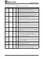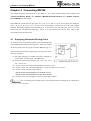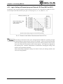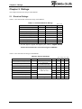
1
STD-CU46-V1.3E CUnet CUnet I/O-IC MKY46 User’s Manual Note 1. The information in this document is subject to change without prior notice. Before using this product, please confirm that this is the latest version of this document. 2. Technical information in this document, such as explanations and circuit examples, are references for this product. When actually using this product, always fully evaluate the entire system according to the design purpose based on considerations of peripheral circuits and the PC board environment. We assume no responsibility for any incompatibility between this product and your system. 3. We assume no responsibility whatsoever for any losses or damages arising from the use of the information, products, and circuits in this document, or for infringement of patents and any other rights of a third party. 4. When using this product and the information and circuits in this document, we do not guarantee the right to use any property rights, intellectual property rights, and any other rights of a third party. 5. This product is not designed for use in critical applications, such as life support systems. Contact us when considering such applications. 6. No part of this document may be copied or reproduced in any form or by any means without prior written permission from StepTechnica Co., Ltd.. MKY46 User’s Manual Preface This manual describes the MKY46, or a kind of CUnet I/O-IC. Be sure to read “CUnet Introduction Guide” before understanding this manual and the MKY46. z Target Readers This manual is for: y Those who first build a CUnet y Those who first use StepTechnica's various ICs to build a CUnet z Prerequisites This manual assumes that you are familiar with: y Network technology y Semiconductor products (especially microcontrollers and memory) z Related Manuals y CUnet Introduction Guide y CUnet Technical Guide [Caution] y To users with “CUnet User’s Manual” released before March, 2001 Some terms in this manual have been changed to conform to International Standards. y Some terms in this manual are different from those used on our website and in our product brochures. The brochure uses ordinary terms to help many people in various industries understand our products. Please understand technical information on HLS Family and CUnet Family based on technical documents (manuals). This manual has been prepared based on Standard EnglishTM meeting the requirements of the International Organization for Standardization (ISO) and the American National Standards Institute (ANSI). This English manual is consistent with the Japanese document “STD-CU46V1.3J”. y Standard English is a trademark of Win Corporation. - iii - MKY46 User’s Manual - iv - MKY46 User’s Manual CONTENTS Chapter 1 MKY46 Role and Features 1.1 Station in MKY46 (I/O Station).............................................................................. 1-3 1.2 Response Speed and Quality of I/O Signals....................................................... 1-4 1.3 Features of MKY46 ................................................................................................ 1-4 Chapter 2 MKY46 Hardware ................................................................................2-3 Chapter 3 Operation of MKY46 3.1 Internal Configuration of MKY46 ......................................................................... 3-3 3.2 Sending of Internal Input Pin Data....................................................................... 3-4 3.3 Data Updating of Internal Output Pins ................................................................ 3-4 3.4 Operation of General-purpose External I/O Pins (Io0 to Io31) and Multi-selector 3-5 3.5 Selection of Data Output to Internal Output Pins............................................... 3-7 3.6 Data Structure of Owned Memory Block............................................................. 3-8 3.7 Support for Phase Transition............................................................................... 3-9 3.7.1 Operation in RUN Phase ............................................................................................. 3-9 3.7.2 Operation in CALL Phase ......................................................................................... 3-10 3.7.3 Operation in BREAK Phase ...................................................................................... 3-10 3.7.4 Support for Resizing ................................................................................................. 3-11 3.7.5 Network Stop and Restart......................................................................................... 3-11 3.8 Cycle Time of CUnet ........................................................................................... 3-12 3.9 Support for Frame Option [for HUB] ................................................................. 3-13 3.9.1 Cautions for Setting of Frame Option ..................................................................... 3-13 3.9.2 Number of Insertable HUBs...................................................................................... 3-14 Chapter 4 Connecting MKY46 4.1 Supplying Generated Driving Clock .................................................................... 4-3 4.2 Hardware Reset ..................................................................................................... 4-4 4.3 Connecting Network Interface ............................................................................. 4-5 4.3.1 Recommended Network Connection......................................................................... 4-5 4.3.2 Details of RXD, TXE, and TXD Pins............................................................................ 4-5 4.4 Setting Baud Rate ................................................................................................. 4-6 4.5 Network Cable Length .......................................................................................... 4-7 4.6 Setting of Frame Option (#LFS) ........................................................................... 4-7 4.7 Setting Station Addresses.................................................................................... 4-8 - v - MKY46 User’s Manual 4.8 Selection of Data Output to Internal Output Pins (#DOSA0 to #DOSA5, #DOHL)... 4-9 4.9 Input/Output Setting of General-purpose External I/O Pins (IOS0 to IOS2, #IOSWAP).................................................................................... 4-10 4.10 Logic Setting of General-purpose External I/O Pins (INV0 to INV7) ............... 4-11 4.11 Connection of General-purpose External I/O Pins........................................... 4-12 4.12 Use of Timing Notification Signals (STB1, STB2) ............................................ 4-12 4.13 Use of Signal for Notifying Output Availability of General-purpose External I/O Pins (DOA)......................................................... 4-12 4.14 Indicating Output Availability of General-purpose External I/O Pins (DONA).. 4-13 4.15 Clearing Output Level of General-purpose External I/O Pins (#CLRH, #CLRL).. 4-13 4.16 Clearing Output by Watchdog Timer................................................................. 4-14 4.17 Indicating Input Data Sending Status of General-purpose External I/O Pins (#MON) ...................................................... 4-14 4.18 Notifying Start Timing of Cycle (#CYCT Pin) .................................................... 4-15 4.19 Notifying Reception of PING Instruction (PlNG) .............................................. 4-15 4.20 Schematic Connection Diagram ........................................................................ 4-16 4.21 Configuration Using Only I/O Stations.............................................................. 4-17 4.21.1 Cycle Time Only for I/O Station................................................................................ 4-18 4.21.2 Use of #IOSWAP Pin ................................................................................................. 4-18 4.21.3 Use of #LFS (Long Frame Select) Pin [for HUB]..................................................... 4-19 Chapter 5 Ratings 5.1 Electrical Ratings .................................................................................................. 5-3 5.2 AC Characteristics ................................................................................................ 5-4 5.2.1 Clock and Reset Timing (#RST, Xi)............................................................................ 5-4 5.2.2 Baud Rate Timing (TXE, TXD, RXD)........................................................................... 5-5 5.2.3 Transfer Timing when External Clock (EXC) Used................................................... 5-5 5.2.4 Output Timing of #CYCT............................................................................................. 5-6 5.2.5 STB1, STB2 and Data IO Pin Timing.......................................................................... 5-6 5.3 Package Dimensions ............................................................................................ 5-7 5.4 Recommended Soldering Conditions ................................................................. 5-8 5.5 Recommended Reflow Conditions ...................................................................... 5-8 Appendix Appendix 1 Cycle Time Table ................................................................................ App-3 Appendix 2 Internal Equivalent Block Diagram ................................................... App-4 Appendix 3 Differences between MKY46 and MKY40 in IO mode...................... App-5 - vi - MKY46 User’s Manual Figures Fig. 1.1 I/O Station ..................................................................................................... 1-3 Fig. 1.2 CUnet Connecting Two Modes ................................................................... 1-3 Fig. 2.1 MKY46 Pin Assignment ............................................................................... 2-3 Fig. 2.2 Pin Electrical Characteristics in I/O Circuit Types in MKY46................... 2-8 Fig. 3.1 Internal Configuration of MKY46 ................................................................ 3-3 Fig. 3.2 Internal Configuration of Multi-selector (for One Io Pin).......................... 3-5 Fig. 3.3 Selection of Data Output to Internal Output Pins ..................................... 3-7 Fig. 3.4 Number of Inserted HUBs ......................................................................... 3-14 Fig. 4.1 Supplying Generated Driving Clock........................................................... 4-3 Fig. 4.2 Hardware Reset ............................................................................................ 4-4 Fig. 4.3 Recommended Network Connection ......................................................... 4-5 Fig. 4.4 Setting of Baud Rate.................................................................................... 4-6 Fig. 4.5 Setting Example of Station Addresses ...................................................... 4-8 Fig. 4.6 Setting Example of #DOSA0 to #DOSA5 Pins and #DOHL Pin................ 4-9 Fig. 4.7 Input/Output Setting Example of General-purpose External I/O Pins... 4-10 Fig. 4.8 Example of Logic Setting of General-purpose External I/O Pins .......... 4-11 Fig. 4.9 Example of LED Connection to DONA Pin .............................................. 4-13 Fig. 4.10 Example of Clearing Output by Watchdog .............................................. 4-14 Fig. 4.11 Example of LED Connection to #MON Pin............................................... 4-14 Fig. 4.12 Pin Setting and Connection Concept....................................................... 4-16 Fig. 4.13 CUnet Configured Only by I/O Stations ................................................... 4-17 Fig. 4.14 Concept of System Where Multiple I/O Signals Can Be Connected with One Network Cable ........................................... 4-17 Fig. 4.15 Concept of Use of #IOSWAP Pin .............................................................. 4-18 - vii - MKY46 User’s Manual Tables Table 2-1 Pin Functions of MKY46 .............................................................................. 2-4 Table 2-2 Electrical Ratings of MKY46........................................................................ 2-7 Table 3-1 General-purpose External I/O Pins Corresponding to INV0 to INV7 ....... 3-5 Table 3-2 Input/Output and Connection of General-purpose External I/O Pins...... 3-6 Table 3-3 Data Structure of Owned Memory Block (MB) .......................................... 3-8 Table 4-1 Network Cable Length ................................................................................. 4-7 Table 4-2 Cycle Time with FS = 63 ............................................................................ 4-18 Table 4-3 Frame-option-set Cycle Time with FS = 63.............................................. 4-19 Table 5-1 Absolute Maximum Ratings ........................................................................ 5-3 Table 5-2 Electrical Ratings ......................................................................................... 5-3 Table 5-3 AC Characteristics Measurement Conditions ........................................... 5-4 - viii - Chapter 1 MKY46 Role and Features This chapter describes the role and features of the MKY46 in CUnet. 1.1 Station in MKY46 (I/O Station) ......................................................1-3 1.2 Response Speed and Quality of I/O Signals ...............................1-4 1.3 Features of MKY46 ........................................................................1-4 Chapter 1 MKY46 Role and Features Chapter 1 MKY46 Role and Features This chapter describes the role and features of the MKY46 in the CUnet. The MKY46 is a CUnet-dedicated I/O-IC with the CUnet protocol based on full hard-wire logic packaged in a 100-pin TQFP using CMOS technology. The MKY46 is a CUnet-dedicated I/O-IC (CUnet I/O-IC) providing backward compatibility with the IO mode of previously released MKY40. This manual describes a “CUnet station” which mounts the MKY46 in the CUnet system as “I/O station”. 1.1 Station in MKY46 (I/O Station) The MKY46 can connect its general-purpose external I/O pin signals (I/O signals) directly to Global Memory (GM) of the CUnet system by connecting a network I/F to a network (Fig. 1.1). The CUnet system in Figure 1.2 consists of two MEM stations and two I/O stations. Each MEM station has a MKY40 (MEM mode) that can access GM and the user CPU. Each I/O station has a MKY46 (CUnet I/O-IC). In the CUnet system, all user CPUs can read the state of input ports of the I/O stations from GM. User CPUs can also set the state of output ports of the I/ O stations. 1-3 MKY46 User’s Manual 1.2 Response Speed and Quality of I/O Signals In the case where the CUnet system to which the MKY46 is connected operates normally, a signal connected to the input pin of the MKY46 general-purpose I/O pins is copied to all the CUnet stations at every cycle by the CUnet protocols. In addition, the state of the output pin of the MKY46 general-purpose I/O pins is updated at every time when the copied data for each cycle is received from other specified CUnet station. Another CUnet station connected to a network can reference and control the I/O signal of the MKY46 general-purpose I/O pins, as a minimum unit of one cycle of the CUnet. Therefore, the signal response speed of the MKY46 general-purpose I/O pins is the same as the cycle time of the CUnet. When a network consists of two stations, the cycle time of the CUnet is 120μs (when 12 Mbps selected). Even when it consists of 30 stations, the cycle time is within 1 ms (when 12 Mbps selected) and very fast. Also, the cycle time of the CUnet can be calculated using an equation and the calculated value is always constant. Furthermore, data copied between the CUnet stations is strictly controlled and its quality is also assured. So the I/O signals of the MKY46 general-purpose pins can be used as signals to control various equipment or systems. For details on the cycle time of the CUnet, refer to “CUnet Introduction Guide”, “3.8 Cycle Time of CUnet” and “Appendix 1 Cycle Time Table” in this manual. For data quality assurance, refer to “CUnet Introduction Guide”. 1.3 Features of MKY46 The MKY46 has the same features as the IO mode of previously released MKY40. (1) Can be connected to up to 64 CUnet stations (2) Occupies one memory block (8 bytes) in GM (3) Standard baud rates of 12, 6, and 3 Mbps (4) Has 32 general-purpose external I/O pins that can be selected between “input” and “output” every 4 bits and the logic between pin levels and data can be inverted (5) Has various pins for timing output and LED indication that can be easily expanded and applied by user application (6) Can configure CUnet system using only I/O stations (7) The CUnet protocol of the MKY46 guarantees that I/O data can be treated by general-purpose external I/O pins without error or garbage (1) For the differences between the MKY46 and MKY40 in IO mode, refer to “Appendix 3 Differences Between MKY46 and MKY40 in IO mode” which will help determine if the MKY46 can be mounted on a board for the MKY40 in IO mode. (2) The MKY46 has no microcontroller, so program runaway cannot occur. 1-4 Chapter 2 MKY46 Hardware This chapter describes the MKY46 hardware such as pin assignment, pin functions, and input/output circuit types. Chapter 2 MKY46 Hardware Chapter 2 MKY46 Hardware This chapter describes the MKY46 hardware such as pin assignment, pin functions, and input/output circuit types. Figure 2.1 shows the MKY46 pin assignment. 2-3 MKY46 User’s Manual Table 2-1 lists the pin functions of the MKY46. Table 2-1 Pin Functions of MKY46 Pin name PING DOA #CLRH #CLRL #LFS #DOHL Pin No. 7 8 9 10 11 12 Logic Positive Positive Negative Negative Negative Negative I/O Function O Output pin with PING function that goes High when PING instruction received from other CUnet stations If a hardware reset is activated, this pin is kept Low in preference to the PING instruction from other CUnet stations. O Output pin to notify that data in Io0 to Io31 pins set to “output” by setting of IOS0 to IOS2 pins updated within a given time If data is updated within a given time, this pin is kept High. When a hardware reset is activated, this pin is kept Low. I Input pin to force Io16 to Io31 pins set to “output” by setting of IOS0 to IOS2 pins to specific level When the input of this pin is Low, the last-stage latch of Io16 to Io31 pins set to “output” is cleared to “0”. The Io16 to Io31 pins output High or Low according to the setting of the INV4 to INV7 pins. I Input pin to force Io0 to Io15 pins set to “output” by setting of IOS0 to IOS2 pins to specific level When the input of this pin is Low, the last-stage latch of Io0 to Io15 pins set to “output” is cleared to “0”. The Io0 to Io15 pins output High or Low according to the setting of INV0 to INV3 pins. I Input pin to set to frame option Usually, fix this pin at High. Fix this pin at Low only when constructing a CUnet just using IO stations and setting the MKY46 to a long frame (LF). I Input pin to set whether to select upper bits (bits 32 to 63) or lower bits (bits 0 to 31) of Memory Blocks (MBs) selected by #DOSA0 to #DOSA5 pins for data to be output to Io0 to Io31 pins set to “output” by setting of IOS0 to IOS2 pins The lower bits are selected when this pin is High and the upper bits are selected when the pin is Low. INV0 to INV7 13 to 20 Positive I Input pins to reverse internal logic and pin levels of Io0 to Io31 pins When these pins are Low, the Io0 to Io31 pins at internal logic “1” are High. When these pins are High, the Io0 to Io31 pins at internal logic “0” are High. IOS0 to IOS2 21 to 23 Positive I Input pins to set Io0 to Io31 pins to “input” or “output” Io0 to Io31 pins are set to “input” or “output” by combining High and Low level inputs to these pins. I Input pin for MKY46 hardware reset Immediately after power-on or when the user intentionally resets hardware, keep this pin Low for 10 or more clocks of the frequency of the Xi pin. Usually keep this pin High. #RST 24 Negative (Continue) 2-4 Chapter 2 MKY46 Hardware Table 2-1 Pin Functions of MKY46 Pin name #IOSWAP Pin No. 27 Logic Negative (Continued) I/O Function I Input pin to reverse “input” or “output” status of Io0 to Io31 pins determined by setting of IOS0 to IOS2 pins The status is not reversed when this bit is High. When this pin is Low, the status of Io0 to Io31 pins determined by the setting of IOS0 to IOS2 pins is reversed from “input” to “output” and from “output” to “input”. STB1 28 Positive O Output pin to notify when to update data in Io0 to Io31 pins set to “output” by setting of IOS0 to IOS2 pins This pin usually outputs a Low level and a High level for a given time at updating data. Io0 to Io7 Io8 to Io15 Io16 to Io23 Io24 to Io31 29 to 36 42 to 49 53 to 60 64 to 71 Positive/ Negative I/O 32-bit general-purpose external I/O pins Positive or negative logic depends on the setting of the INV0 to INV7 pins. STB2 41 Positive O Output pin to notify when to internally write data in Io0 to Io31 pins set to “input” by setting of IOS0 to IOS2 pins This pin usually outputs a Low level and a High level for a predetermined time when writing data internally. #CYCT 52 Negative O Output pin to notify timing that outputs Low level for a given time at the beginning of cycle time. RXD 77 Positive I Input pin to input packets Connect this pin to the receiver output pin. TXE 78 Positive O Output pin to output High level during outputting packets to be sent Connect this pin to the enable input pin of a driver. TXD 79 Positive O Output pin to output packets to be sent Connect this pin to the drive input pin of a driver. #SA0 to #SA5 80 to 85 Negative I Input pin to set station addresses (SAs) When a hardware reset is activated, the MKY46 writes the inverted state of this pin into the internal circuit. #DOSA0 to #DOSA5 86 to 91 Negative I Input pins to select Memory Block (MB) to output to Io0 to Io31 pins set to “output” by setting of IOS0 to IOS2 pins Set the MB numbers (00H to 3FH) as 6-bit negative logic binary values (3FH to 00H). #MON 92 Negative O Output pin for lighting LED to output Low level while stable link with other CUnet stations is established O Output pin to notify that data in Io0 to Io31 pins set to “output” by setting of IOS0 to IOS2 pins not updated within a given time If data is not updated within a given time, this pin keeps output High. (This pin is the reverse output of the DOA pin. It outputs a Low level when the DOA pin High and a High level when the DOA pin is Low). When a hardware reset is activated, this pin is kept High. I Clock input pin that is used as baud rate depends on external clock The baud rate is “1/4” of the supply frequency, up to 12.5 MHz. Fix this pin at High or Low when it is not used. DONA EXC 93 95 Positive Positive (Continue) 2-5 MKY46 User’s Manual Table 2-1 Pin Functions of MKY46 Pin name Pin No. BPS0 BPS1 96 97 Xi Logic (Continued) I/O Function Positive I Input pin to set baud rates When a hardware reset is activated, the MKY46 writes the status of this pin into the internal circuit. 99 Positive I Pin for connection of generated clock VDD 26, 37 50, 61 76, 100 --- --- Power pins for 5.0-V supply GND 1, 25 38, 40 51, 62 72 to 75 --- --- Power pins connected to 0 V N.C. 2, 6, 63, 94, 98 --- O Non-functional unconnected pins Not connected into the internal circuit. N.C. 3 to 5 --- O Non-functional output pins Leave these output pins open. Note: Pins prefixed with # are negative logic (active Low). 2-6 Chapter 2 MKY46 Hardware Table 2-2 shows the electrical ratings of the MKY46. Table 2-2 Electrical Ratings of MKY46 (#: Negative logic) No I/O Name Type No I/O Name Type No I/O Name Type No I/O Name 1 -- GND -- 26 -- VDD -- 51 -- GND -- 76 -- VDD Type -- 2 -- N.C. -- 27 I #IOSWAP B 52 O #CYCT E 77 I RXD D F 3 O N.C. E 28 O STB1 E 53 I/O Io16 G 78 O TXE 4 O N.C. E 29 I/O Io0 G 54 I/O Io17 G 79 O TXD F 5 O N.C. E 30 I/O Io1 G 55 I/O Io18 G 80 I #SA0 C 6 -- N.C. -- 31 I/O Io2 G 56 I/O Io19 G 81 I #SA1 C 7 O PING E 32 I/O Io3 G 57 I/O Io20 G 82 I #SA2 C 8 O DOA E 33 I/O Io4 G 58 I/O Io21 G 83 I #SA3 C 9 I #CLRH C 34 I/O Io5 G 59 I/O Io22 G 84 I #SA4 C 10 I #CLRL C 35 I/O Io6 G 60 I/O Io23 G 85 I #SA5 C 11 I #LFS B 36 I/O Io7 G 61 -- VDD -- 86 I #DOSA0 C 12 I #DOHL B 37 -- VDD -- 62 -- GND -- 87 I #DOSA1 C 13 I INV0 B 38 -- GND -- 63 -- N.C. -- 88 I #DOSA2 C 14 I INV1 B 39 -- GND -- 64 I/O Io24 G 89 I #DOSA3 C 15 I INV2 B 40 I GND B 65 I/O Io25 G 90 I #DOSA4 C 16 I INV3 B 41 O STB2 E 66 I/O Io26 G 91 I #DOSA5 C 17 I INV4 B 42 I/O Io8 G 67 I/O Io27 G 92 O #MON F 18 I INV5 B 43 I/O Io9 G 68 I/O Io28 G 93 O DONA F 19 I INV6 B 44 I/O Io10 G 69 I/O Io29 G 94 -- N.C. -- 20 I INV7 B 45 I/O Io11 G 70 I/O Io30 G 95 I EXC D 21 I IOS0 B 46 I/O Io12 G 71 I/O Io31 G 96 I BPS0 C 22 I IOS1 B 47 I/O Io13 G 72 -- GND -- 97 I BPS1 C 23 I IOS2 B 48 I/O Io14 G 73 -- GND -- 98 -- N.C. -- 24 I #RST D 49 I/O Io15 G 74 -- GND -- 99 I Xi B 25 -- GND -- 50 -- VDD -- 75 -- GND -- 100 -- VDD -- 2-7 MKY46 User’s Manual Figure 2.2 shows the electrical characteristics of the MKY46 pins. 2-8 Chapter 3 Operation of MKY46 This chapter describes the operation of the MKY46. For a better understanding of this chapter, read “CUnet Introduction Guide” and “Chapter 1 MKY46 Role and Features”. 3.1 Internal Configuration of MKY46..................................................3-3 3.2 Sending of Internal Input Pin Data ...............................................3-4 3.3 Data Updating of Internal Output Pins.........................................3-4 3.4 Operation of General-purpose External I/O Pins (Io0 to Io31) and Multi-selector ..........................................................................3-5 3.5 Selection of Data Output to Internal Output Pins .......................3-7 3.6 Data Structure of Owned Memory Block .....................................3-8 3.7 Support for Phase Transition .......................................................3-9 3.8 Cycle Time of CUnet....................................................................3-12 3.9 Support for Frame Option [for HUB]..........................................3-13 Chapter 3 Operation of MKY46 Chapter 3 Operation of MKY46 This chapter describes the operation of the MKY46. For a better understanding of this chapter, read “CUnet Introduction Guide” and “Chapter 1 MKY46 Role and Features”. In the MKY46, Station Addresses (SAs) must be set to the #SA0 to #SA5 pins by combining High or Low levels that the user inputs and owns one Memory Block (MB) corresponding to the SA. 3.1 Internal Configuration of MKY46 The MKY46 has 32-bit internal input pins (Di0 to Di31) and 32-bit internal output pins (Do0 to Do31) as well as a CUnet IC core. The 32-bit internal input pins (Di0 to Di31) and 32-bit internal output pins (Do0 to Do31) are connected to general-purpose external I/O pins (Io0 to Io31) using a multi-selector (Fig. 3.1). The schematic diagram is shown in “Appendix 2 Internal Equivalent Block Diagram”. 3-3 MKY46 User’s Manual 3.2 Sending of Internal Input Pin Data The MKY46 sends data of internal input pins (Di0 to Di31) to Global Memory (GM) in other CUnet stations as follows (Fig. 3.1): (1) The MKY46 generates an STB2 (input update strobe) signal at the lead point of sending packet determined by the Station Address (SA). (2) The MKY46 samples data in internal input pins (Di0 to Di31) with the STB2 signal. The sampled data is allocated in the lower 32 bits of an owned Memory Block (MB). (3) The status of each setting pin is embedded in the upper 32 bits of the owned MB. (4) The latest data (data in (2) and (3) above) in the MB owned by the MKY46 is sent to GM in all CUnet stations in accordance with the CUnet protocol. Because the STB2 signal is output to external pins, the user can recognize the input sampling time. 3.3 Data Updating of Internal Output Pins The MKY46 updates data in MBs owned by other CUnet stations as data in internal output pins (Do0 to Do31) as follows (Fig. 3.1): (1) The MKY46 generates a receive strobe signal when receiving packets sent from other CUnet stations to update data in MBs. (2) In this case, either of the upper 32 bits or the lower 32 bits of receive data (64 bits) for update in the received MB is input to two 16-bit latches according to the levels (High or Low) input to the #DOHL pin. (3) An MB is selected by the combination of High or Low levels that the user inputs to the #DOSA0 to #DOSA5 pins. If a received packet is data in this MB, an STB1 (output update strobe) signal is generated from the receive strobe signal. The MKY46 drives two 16-bit latches with this STB1 signal to update data in internal output pins (Do0 to Do31). (4) When the user inputs a Low level to the #CLRL pin, the lower 16 bits of data in internal output pins (Do0 to Do31) can be cleared forcibly to Low level in preference to the (3) above. (5) When the user inputs a Low level to the #CLRH pin, the upper 16 bits of data in internal output pins (Do0 to Do31) can be cleared forcibly to Low level in preference to (3) above. (6) When a hardware reset is activated, data in internal output pins (Do0 to Do31) is cleared forcibly to Low level in preference to (3) above. Because the STB1 signal is output to external pins, the user can recognize the output updating time. 3-4 Chapter 3 Operation of MKY46 3.4 Operation of General-purpose External I/O Pins (Io0 to Io31) and Multi-selector The general-purpose external I/O pins (Io0 to Io31) are connected to 32-bit internal input pins (Di0 to Di31) or 32-bit internal output pin (Do0 to Do31) using a multi-selector (Fig. 3.1). The multi-selector functions by the combination of High or Low levels that the user inputs to the IOS0 to IOS2 pins, the #IOSWAP pin, and INV0 to INV7 pins. Figure 3.2 shows the internal configuration of a selector corresponding to one Io pin. The multi-selector has 32 selectors with the configuration shown in Figure 3.2. IOS0 to IOS2 are input pins that select general-purpose external I/O pins (Io0 to Io31) as “input” and “output”. #IOSWAP is an input pin that reverses input and output determined by IOS0 to IOS2. Table 3-2 indicates the input and output selection by IOS0 to IOS2 and #IOSWAP. INV0 to INV7 are input pins that set the relationship between internal logic and the logic of general-purpose external I/O pin (Io0 to Io31) levels. For example, when the INV0 pin is Low, internal logic “1” corresponding to the Io0 to Io3 pins is the pin High level and internal logic “0” is the pin Low level. When the INV0 pin is High, internal logic “1” corresponding to the Io0 to Io3 pins is the pin Low level and internal logic “0” is the pin High level. Table 3-1 lists the general-purpose external I/O pins (Io0 to Io31) corresponding to INV0 to INV7. Table 3-1 General-purpose External I/O Pins Corresponding to INV0 to INV7 INV Pin Name Corresponding general-purpose external I/O pin INV0 Io0 to Io3 INV1 Io4 to Io7 INV2 Io8 to Io11 INV3 Io12 to Io15 INV4 Io16 to Io19 INV5 Io20 to Io23 INV6 Io24 to Io27 INV7 Io28 to Io31 3-5 MKY46 User’s Manual Table 3-2 Input/Output and Connection of General-purpose External I/O Pins When #IOSWAP pin is High Pin name When #IOSWAP pin is Low Pin name Setting level Setting level IOS2 Lo Lo Lo Lo Hi Hi Hi Hi IOS2 Lo Lo Lo Lo Hi Hi Hi Hi IOS1 Lo Lo Hi Hi Lo Lo Hi Hi IOS1 Lo Lo Hi Hi Lo Lo Hi Hi IOS0 Lo Hi Lo Hi Lo Hi Lo Hi IOS0 Lo Hi Lo Hi Lo Hi Lo Hi Pin name Pin name Input/output Input/output Io0 Di0 Di0 Di0 Di0 Di0 Di0 Di0 Do0 Io0 Do0 Do0 Do0 Do0 Do0 Do0 Do0 Di0 Io1 Di1 Di1 Di1 Di1 Di1 Di1 Di1 Do1 Io1 Do1 Do1 Do1 Do1 Do1 Do1 Do1 Di1 Io2 Di2 Di2 Di2 Di2 Di2 Di2 Di2 Do2 Io2 Do2 Do2 Do2 Do2 Do2 Do2 Do2 Di2 Io3 Di3 Di3 Di3 Di3 Di3 Di3 Di3 Do3 Io3 Do3 Do3 Do3 Do3 Do3 Do3 Do3 Di3 Io4 Di4 Di4 Di4 Di4 Di4 Di4 Di4 Do4 Io4 Do4 Do4 Do4 Do4 Do4 Do4 Do4 Di4 Io5 Di5 Di5 Di5 Di5 Di5 Di5 Di5 Do5 Io5 Do5 Do5 Do5 Do5 Do5 Do5 Do5 Di5 Io6 Di6 Di6 Di6 Di6 Di6 Di6 Di6 Do6 Io6 Do6 Do6 Do6 Do6 Do6 Do6 Do6 Di6 Io7 Di7 Di7 Di7 Di7 Di7 Di7 Di7 Do7 Io7 Do7 Do7 Do7 Do7 Do7 Do7 Do7 Di7 Io8 Di8 Di8 Di8 Di8 Di8 Di8 Do8 Do8 Io8 Do8 Do8 Do8 Do8 Do8 Do8 Di8 Di8 Io9 Di9 Di9 Di9 Di9 Di9 Di9 Do9 Do9 Io9 Do9 Do9 Do9 Do9 Do9 Do9 Di9 Di9 Io19 Di10 Di10 Di10 Di10 Di10 Di10 Do10 Do10 Io19 Do10 Do10 Do10 Do10 Do10 Do10 Di10 Di10 Io11 Di11 Di11 Di11 Di11 Di11 Di11 Do11 Do11 Io11 Do11 Do11 Do11 Do11 Do11 Do11 Di11 Di11 Io12 Di12 Di12 Di12 Di12 Di12 Do12 Do12 Do12 Io12 Do12 Do12 Do12 Do12 Do12 Di12 Di12 Di12 Io13 Di13 Di13 Di13 Di13 Di13 Do13 Do13 Do13 Io13 Do13 Do13 Do13 Do13 Do13 Di13 Di13 Di13 Io14 Di14 Di14 Di14 Di14 Di14 Do14 Do14 Do14 Io14 Do14 Do14 Do14 Do14 Do14 Di14 Di14 Di14 Io15 Di15 Di15 Di15 Di15 Di15 Do15 Do15 Do15 Io15 Do15 Do15 Do15 Do15 Do15 Di15 Di15 Di15 Io16 Di16 Di16 Di16 Di16 Do16 Do16 Do16 Do16 Io16 Do16 Do16 Do16 Do16 Di16 Di16 Di16 Di16 Io17 Di17 Di17 Di17 Di17 Do17 Do17 Do17 Do17 Io17 Do17 Do17 Do17 Do17 Di17 Di17 Di17 Di17 Io18 Di18 Di18 Di18 Di18 Do18 Do18 Do18 Do18 Io18 Do18 Do18 Do18 Do18 Di18 Di18 Di18 Di18 Io19 D19 D19 D19 D19 Do19 Do19 Do19 Do19 Io19 Do19 Do19 Do19 Do19 D19 D19 D19 D19 Io20 Di20 Di20 Di20 Do20 Do20 Do20 Do20 Do20 Io20 Do20 Do20 Do20 Di20 Di20 Di20 Di20 Di20 Io21 Di21 Di21 Di21 Do21 Do21 Do21 Do21 Do21 Io21 Do21 Do21 Do21 Di21 Di21 Di21 Di21 Di21 Io22 Di22 Di22 Di22 Do22 Do22 Do22 Do22 Do22 Io22 Do22 Do22 Do22 Di22 Di22 Di22 Di22 Di22 Io23 Di23 Di23 Di23 Do23 Do23 Do23 Do23 Do23 Io23 Do23 Do23 Do23 Di23 Di23 Di23 Di23 Di23 Io24 Di24 Di24 Do24 Do24 Do24 Do24 Do24 Do24 Io24 Do24 Do24 Di24 Di24 Di24 Di24 Di24 Di24 Io25 Di25 Di25 Do25 Do25 Do25 Do25 Do25 Do25 Io25 Do25 Do25 Di25 Di25 Di25 Di25 Di25 Di25 Io26 Di26 Di26 Do26 Do26 Do26 Do26 Do26 Do26 Io26 Do26 Do26 Di26 Di26 Di26 Di26 Di26 Di26 Io27 Di27 Di27 Do27 Do27 Do27 Do27 Do27 Do27 Io27 Do27 Do27 Di27 Di27 Di27 Di27 Di27 Di27 Io28 Di28 Do28 Do28 Do28 Do28 Do28 Do28 Do28 Io28 Do28 Di28 Di28 Di28 Di28 Di28 Di28 Di28 Io29 Di29 Do29 Do29 Do29 Do29 Do29 Do29 Do29 Io29 Do29 Di29 Di29 Di29 Di29 Di29 Di29 Di29 Io30 Di30 Do30 Do30 Do30 Do30 Do30 Do30 Do30 Io30 Do30 Di30 Di30 Di30 Di30 Di30 Di30 Di30 Io31 Di31 Do31 Do31 Do31 Do31 Do31 Do31 Do31 Io31 Do31 Di31 Di31 Di31 Di31 Di31 Di31 Di31 “Dixx” in the table indicates input, and “Doxx” indicates output. 3-6 Chapter 3 Operation of MKY46 3.5 Selection of Data Output to Internal Output Pins Select data to be output to internal output pins by the #DOSA0 to #DOSA5 pins and #DOHL pin. Figure 3.3 shows the concept of data selected by pin setting. When packets from the CUnet station matching the setting of #DOSA0 to #DOSA5 pins are received, data in internal output pins is updated (refer to “3.3 Data Updating of Internal Output Pins”). Internal output pins (Do0 to Do31) are Low until packets are received from the CUnet station matching the setting of the #DOSA0 to #DOSA5 pins after hardware reset. If the CUnet station matching the setting of the #DOSA0 to #DOSA5 pins is not connected to a network, the output is not updated. 3-7 MKY46 User’s Manual 3.6 Data Structure of Owned Memory Block The following data is embedded in the Memory Block (MB) owned by the MKY46 set by the #SA0 to #SA5 pins (Table 3-3). (1) Bits 0 to 31: Data in internal input pins (Di0 to Di31) (2) Bits 32 to 34: Setting of IOS0 to IOS2 pins (3) Bit 35: Setting of #IOSWAP pin (4) Bits 36 to 38: Always “0” (5) Bit 39: Setting of #LFS pin (6) Bit 40: Setting of #DOHL pin (7) Bits 41 to 46: Setting of #DOSA0 to #DOSA5 pins (8) Bit 47: Always “0” (9) Bits 48 to 55: Setting of INV0 to INV7 pins (10) Bits 56 to 63: Always “0” Bits 0 to 31 where data in internal input pins in (1) above is stored go to “0”, if corresponding general-purpose external I/O pins (Io0 to Io31) are not set to “input” (bits set to “output”) (Fig. 3.2). Items (3), (5), (6), and (7) above are negative-logic input pins. Reversed positive-logic setting states are embedded in the bits of the MB. For example, bit 35 goes to “1” when the #IOSWAP pin is Low and “0” when the pin is High (for this reason, no # symbol is shown in Table 3-3). Data in an MB that is owned by the MKY46 is sent to all other CUnet stations connected to a network. This enables all other CUnet stations connected to a network to recognize the pin setting states as well as data in internal input pins (Di0 to Di31). Table 3-3 Data Structure of Owned Memory Block (MB) 3-8 Chapter 3 Operation of MKY46 3.7 Support for Phase Transition The MKY46 has START, CALL, RUN, and BREAK phases. In the MKY46, a network is started immediately after a hardware reset is released from being activated, the user system needs not start the network. When a hardware reset is released from being activated, the MKY46 changes to any of the CALL, RUN, and BREAK phases after two or three cycle times in the START phase when a network is started. An I/O station is used just as an input/output equipment. Which phase the MKY46 is in is not indicated for the user system. 3.7.1 Operation in RUN Phase The RUN phase is a normal operating state of a CUnet. A link with other CUnet stations connected to a network is performed constantly. Regarding the state where a link defined in the CUnet protocol is consecutively established three or more times as a link with other CUnet stations being stable, “the MKY46 outputs a Low level to the #MON pin. When the MKY46 is in the RUN phase, packets are periodically sent to send the setting state of and data in internal input pins (Di0 to Di31) to a network after the #MON pin changes to a Low level. When CUnet stations at station addresses matching the setting of #DOSA0 to #DOSA5 pins exist among the other linked CUnet stations, the MKY46 outputs pulses from the STB1 pin and updates data in internal output pins (Do0 to Do31). In this case, the standard state of an I/O station has the following features: (1) The #MON pin changes to a Low level. (2) The DOA pin changes to a High level and the DONA pin changes to a Low level. (3) The STB1 pin outputs periodically pulses synchronized with a cycle. (4) The STB2 pin outputs periodically pulses synchronized with a cycle. If CUnet stations at station addresses matching the setting of #DOSA0 to #DOSA5 pins are not started or not connected to a network, pulses are not output from the STB1 pin and data in internal output pins (Do0 to Do31) is not updated. In this case, as compared with the standard features of an I/O station, the I/O station operates as follows: (1) The #MON pin changes to a Low level. (2) The DOA pin remains Low and the DONA pin High. (3) The STB1 pin remains Low (does not output pulses). (4) The STB2 pin outputs periodically pulses synchronized with a cycle. 3-9 MKY46 User’s Manual 3.7.2 Operation in CALL Phase The CALL phase is a state in which a CUnet is waiting to be connected. Only one I/O station connected to a network is started. When the MKY46 is in the CALL phase, packets are sent to send the setting state of and data in internal input pins (Di0 to Di31) to a network. No data in internal output pins (Do0 to Do31) is obtained from a network. In this case, as compared with the standard features of an I/O station, the I/O station operates as follows: (1) The #MON pin remains High. (2) The DOA pin remains Low and the DONA pin High. (3) The STB1 pin remains Low (does not output pulses). (4) The STB2 outputs periodically pulses synchronized with a cycle. The CALL phase is continued until packets can be sent and received to and from other CUnet stations. When other CUnet stations are ready to send and receive packets after a network is started, the MKY46 changes to the RUN phase. 3.7.3 Operation in BREAK Phase The BREAK phase is the state where no access to a cycle is allowed. Because packets are not sent to other CUnet stations connected to a network, the setting state of and data in internal input pins (Di0 to Di31) are not sent to the network. When CUnet stations at station addresses matching the setting of #DOSA0 to #DOSA5 pins operate on a network, pulse are output from the STB1 pin and data in internal output pins (Do0 to Do31) is updated. In this case, as compared with the standard features of an I/O station, the I/O station operates as follows: (1) The #MON pin remains High. (2) The DOA pin changes to a High level and the DONA pin to a Low level. (3) The STB1 pin outputs periodically pulses synchronized with a cycle. (4) The STB2 pin remains Low (does not output pulses). If CUnet stations at station addresses matching the setting of #DOSA0 to #DOSA5 pins do not operate on a network or are not connected to a network, pulses are not output from the STB1 pin and data in internal output pins (Do0 to Do31) is not updated. In this case, as compared with the standard features of an I/O station, the I/O station operates as follows: (1) The #MON pin remains High. (2) The DOA pin remains Low and the DONA pin High. (3) The STB1 pin remains Low (does not output pulses). (4) The STB1 pin remains Low (does not output pulses). The BREAK phase is continued until access to a cycle is allowed by resizing other CUnet stations. When access to a cycle is allowed, the MKY46 changes to the RUN phase. 3 - 10 Chapter 3 Operation of MKY46 3.7.4 Support for Resizing The MKY46 cannot perform resizing. Resizing can be performed from only the CUnet station other than the I/O station (MKY40 in MEM mode). However, when resizing is performed by the CUnet station other than the I/O station, the internal Final Station (FS) values are updated and the MKY46 is resized. 3.7.5 Network Stop and Restart A network consisting of the MKY46 is stopped by the following two cases: (1) SNF (Station Not Found): No link with CUnet stations other than the self-station could be established 32 cycle times consecutively (2) OC (Out of Cycle): Resizing by other CUnet stations caused timing loss to send self-station packets at cyclic time sharing If the network is stopped by the above (1) or (2), the MKY46 is restarted within “8 × TBPS” time. When the network is stopped by (1) SNF (Station Not Found), the MKY46 enters the START phase and then the CALL phase. When the network is stopped by (2) OC (Out of Cycle), the MKY46 enters the START phase and then the BREAK phase. As mentioned above, in the MKY46, the user system needs not start or stop a network. An I/O station consisting of the MKY46 is available just by being connected to a network and capable of hot-swapping. 3 - 11 MKY46 User’s Manual 3.8 Cycle Time of CUnet The cycle time of a CUnet is determined by Equations 3.1 and 3.2 defined by the CUnet protocol. The CUnet cycle time is the response time for memory data sharing. Equation 3.1 Frame Time = (LOF + FS + 1) × 2 × TBPS [s] Equation 3.2 Cycle Time = Frame Time × (FS + PFC + 1) [s] For example, when FS = 03H, LOF = 151, PFC = 2, and baud rate = 12 Mbps (TBPS = (1/12 × 106) ≈ 83.3 ns), the frame time and cycle time are calculated as follows: Frame Time = (151 + 3 + 1 ) × 2 × (1/12 × 106) = 25.833 μs Cycle Time = 25.833 μs × (3 + 2 + 1) = 155 μs In a CUnet, LOF (Length Of Frame) is fixed at “151” and PFC (Public Frame Count) is fixed at “2”. When using the frame option described in “3.9 Support for Frame Option [for HUB]”, the LOF is fixed at “256”. The initial FS (Final Station) value in a CUnet is “63 (3FH)”. The FS value is changed when resizing is performed by the CUnet station other than I/O station. The cycle time at each FS value calculated by Equations 3.1 and 3.2 is shown in “Appendix 1 Cycle Time Table”. For details of resizing, refer to “CUnet Introduction Guide” and another manual of CUnet IC mounted on station other than I/O station. 3 - 12 Chapter 3 Operation of MKY46 3.9 Support for Frame Option [for HUB] The MKY46 conforms to the frame option defined in the CUnet protocol. The frame option causes the Length Of Frame (LOF) to be “256”. This option enables insertion of a HUB (communications cable branching unit) into the CUnet network. The CUnet where a HUB (communications cable branching unit) is inserted into a network provides high degree of flexibility in connecting network cable, resulting in expanded user systems (for details, refer to “HUB-IC User's Manual”) as shown below: (1) Cables in network can be extended (2) Cables in network can be branched (3) Termination resistors at each CUnet station device can be reduced (4) Star topology possible (5) Easy support for optical fibers The LOF of the CUnet in which the frame option is set and operated is “256”. The cycle time gets longer compared to the case where the frame option is not used (refer to “3.8 Cycle Time of CUnet”). 3.9.1 Cautions for Setting of Frame Option The frame option can be set using the #LFS: Long Frame Select pin (pin 11) (refer to “4.6 Setting of Frame Option (#LFS)”). However, when setting the frame option, note the following: (1) The frame option is set to all CUnet stations in the mutual link process with other CUnet stations after network start. (2) It is also set automatically in the CUnet station which is later connected (turned on) to the network operating with the frame option set. (3) Therefore, when the frame option is set to one (or multiple) station(s) connected to a network, the CUnet system changes to a CUnet changes to a CUnet which operates in a cycle with a Length Of Frame (LOF) of “256”. (4) When canceling the frame option for the system, perform an operation to activate a hardware reset for all CUnet ICs in the system. Considering the above, StepTechnica recommends the frame option be set by the CUnet station other than the I/O station (MKY40 in MEM mode) and the use of the #LFS pin (pin 11) be used only in the CUnet system consisting of I/O stations only (refer to “4.21 Configuration Using Only I/O Stations”). 3 - 13 MKY46 User’s Manual 3.9.2 Number of Insertable HUBs In a CUnet network to which the frame option is set, up to two HUBs (communications cable branching units) can be inserted (Fig. 3.4). 3 - 14 Chapter 4 Connecting MKY46 This chapter describes the connection of the MKY46. For a better understanding of this chapter, read “CUnet Introduction Guide”, and “Chapter 1 MKY46 Role and Features” and “Chapter 3 Operation of MKY46” of this manual. 4.1 Supplying Generated Driving Clock ...................................................... 4-3 4.2 Hardware Reset ....................................................................................... 4-4 4.3 Connecting Network Interface ............................................................... 4-5 4.4 Setting Baud Rate ................................................................................... 4-6 4.5 Network Cable Length ............................................................................ 4-7 4.6 Setting of Frame Option (#LFS) ............................................................. 4-7 4.7 Setting Station Addresses...................................................................... 4-8 4.8 Selection of Data Output to Internal Output Pins (#DOSA0 to #DOSA5, #DOHL)............................................................... 4-9 4.9 Input/Output Setting of General-purpose External I/O Pins (IOS0 to IOS2, #IOSWAP)...................................................................... 4-10 4.10 Logic Setting of General-purpose External I/O Pins (INV0 to INV7) . 4-11 4.11 Connection of General-purpose External I/O Pins............................. 4-12 4.12 Use of Timing Notification Signals (STB1, STB2) .............................. 4-12 4.13 Use of Signal for Notifying Output Availability of General-purpose External I/O Pins (DOA)........................................... 4-12 4.14 Indicating Output Availability of General-purpose External I/O Pins (DONA)...................................................................... 4-13 4.15 Clearing Output Level of General-purpose External I/O Pins (#CLRH, #CLRL)....................................................... 4-13 4.16 Clearing Output by Watchdog Timer ................................................... 4-14 4.17 Indicating Input Data Sending Status of General-purpose External I/O Pins (#MON) ........................................ 4-14 4.18 Notifying Start Timing of Cycle (#CYCT Pin) ...................................... 4-15 4.19 Notifying Reception of PING Instruction (PlNG) ................................ 4-15 4.20 Schematic Connection Diagram .......................................................... 4-16 4.21 Configuration Using Only I/O Stations ................................................ 4-17 Chapter 4 Connecting MKY46 Chapter 4 Connecting MKY46 This chapter describes the connection of the MKY46. For a better understanding of this chapter, read “CUnet Introduction Guide”, and “Chapter 1 MKY46 Role and Features” and “Chapter 3 Operation of MKY46” of this manual. In the MKY46, connect the VDD pins (pins 26, 37, 50, 61, 76, 100) to a 5.0-V power supply, the GND pins (pins 1, 25, 38, 39, 40, 51, 62, 72, 73, 74, 75) to a 0-V power supply. Connect a 10 V/0.1 μF (104) or higher capacitor between the adjacent VDD and GND pins. Leave the NC (No Connect) pins (pins 3 to 5) open because they are non-functional output pins. Pins 2, 6, 63, 94, and 98 are also the NC pins. They are not connected into the internal circuit. 4.1 Supplying Generated Driving Clock An external clock (oscillator-generated) can be supplied directly to the MKY46 and used as the driving clock. In this case, supply the driving clock to the Xi pin (pin 99) of the MKY46 (Fig. 4.1). The specifications for direct supplying the driving clock externally are as follows: (1) The upper frequency is 50 MHz and a lower frequency is not provided. Usually supply a 48 MHz clock. (2) Electrical characteristics of the Xi pin: VIH = min. 2.2 V, VIL = max. 0.76 V (3) Connect a clock with a signal rise and fall time of 20 ns or less. (4) Connect a clock with a minimum High level or Low level time of 5 ns or more. (5) Connect a clock with jitter component of: • 250 ps or less at input frequency of 25 MHz or more • 500 ps or less at input frequency of less than 25 MHz (6) Connect a clock with a frequency accuracy of ±500 ppm or better. For a commonly-used oscillator, there is no problem with clock output by the values above in (2) to (6). 4-3 MKY46 User’s Manual 4.2 Hardware Reset When a Low level is input to the #RST (ReSeT) pin (pin 24), the MKY46 is hardware-reset. If a period in which the Low-level signal has been input is less than “one clock”, the signal is ignored to prevent malfunction. To reset the MKY46 completely, the #RST pin must be kept Low for “10 or more clock” while supplying a driving clock. (Fig. 4.2) This manual refers to this state as that “a hardware reset is activated”. Design the circuit so that a hardware reset is surely activated immediately after MKY46 power-on. 4-4 Chapter 4 Connecting MKY46 4.3 Connecting Network Interface The network interface (network I/F) pins of the MKY46 consist of RXD (pin 77), TXE (pin 78), and TXD (pin 79). 4.3.1 Recommended Network Connection Figure 4.3 shows the recommended network connection. The TRX (driver/receiver components) consists of an RS-485-based driver/receiver and a pulse transformer. Recommended network cables include Ethernet LAN cable (10BASE-T, Category 3 or higher) and shielded network cables. Use one twisted-pair cable in the network cable. Depending on the TRX configuration in half-duplex mode, signals output from the TXD pin may be output directly to the RXD pin while the MKY46 transmits packets. However, the MKY46 is designed not to receive any packet transmitted by itself while the TXE pin is High, so there is no problem. Background information to help build a network are described in “CUnet Technical Guide”. For more information about how to select components or to get recommended components, visit our Web site at www.steptechnica.com/. 4.3.2 Details of RXD, TXE, and TXD Pins The MKY46 receives packets transmitted from another CUnet station at the RXD pin and outputs packets transmitted to another CUnet station from the TXD pin. During sending a packet, a High level is output from the TXE pin. When the TXE pin goes High, design the TRX so that the enable pin of the TRX driver is activated, thereby enabling the serial pattern for a packet output from the TXD pin to be transmitted to the network (Fig. 4.3). 4-5 MKY46 User’s Manual 4.4 Setting Baud Rate To set the baud rate of the MKY46, combine High and Low levels to be input to the BPS0 pin (pin 96) and BPS1 pin (pin 97). Figure 4.4 shows the levels of the BPS0 and BPS1 pins corresponding to the baud rates. When a hardware reset is activated, the MKY46 writes these pin settings to the internal circuit. When the “external baud rate” is set, its value is “1/4” of the clock frequency supplied to the EXC pin (pin 95). (For example, if the clock frequency supplied to the EXC pin is 5 MHz, the baud rate is 1.25 Mbps.) The maximum clock frequency to the EXC pin is “12.5 MHz (when Xi = 50 MHz)” with a duty ratio of “40% to 60%”. Always fix the EXC pin at High or Low when not inputting any external clock to the EXC pin. (1) Set the same baud rates to all CUnet devices connected to the network. (2) The EXC pin (pin 95) is an input pin. When not inputting external clocks, fix the EXC pin High or Low and NEVER leave it open. (3) Our recommended pulse transformers may not support baud rates other than “12 Mbps to 3 Mbps”. In this case, use a pulse transformer matching the baud rate. 4-6 Chapter 4 Connecting MKY46 4.5 Network Cable Length In this manual, each connection point of a multi-drop network cable is called a “branch”. Table 4-1 indicates the network cable length for the CUnet when using the network described in “4.3 Connecting Network Interface” with 32 or less branches. Table 4-1 Network Cable Length Baud rate Network cable length 12 Mbps 100 m 6 Mbps 200 m 3 Mbps 300 m The recommended differential driver/receiver is an RS-485-based driver/receiver. Therefore, the branch count “32” stipulated in the RS-485 specification is used as a guide in Table 4-1. Up to 64 CUnet stations can be connected to the CUnet, enabling connection of “64” branches. This recommended network is isolated electrically by a pulse transformer and the format of signals propagated through the network is RZ (Return to Zero). Consequently, “64” branches can be connected using a standard RS485-based driver/receiver without using DC component signals. In this case, the cable length is likely to be shorter than the value in Table 4-1 (due to increase of dispersion of propagated signal energy). Network cable length can be extended by setting the frame option or adding HUB(s). For detail, refer to “3.9 Support for Frame Option [for HUB]” and “User’s Manual” of HUB-IC MKY02. The network cable length varies depending on the cable quality, differential driver/receiver components, cable connection status, and environment. Therefore, values in “Table 4-1 Network Cable Length” are only a guide and performance is not guaranteed. 4.6 Setting of Frame Option (#LFS) The MKY46 has the #LFS: Long Frame Select pin (pin 11) that sets a frame option. When not setting the frame option, fix the #LFS pin at High. When the CUnet is started with the #LFS pin set to Low, the CUnet system is set to the frame option. When setting the frame option (when setting the #LFS pin to Low), refer to “3.9.1 Cautions for Setting of Frame Option”. 4-7 MKY46 User’s Manual 4.7 Setting Station Addresses The #SA0 to #SA5 pins are negative-logic input pins that are pulled up internally. The SAs are given in hexadecimal as “00H to 3FH (addresses 0 to 63)” with a High level input to the #SA0 to #SA5 pins set to “0” and a Low level set to “1”. The most significant bit is #SA5 (pin 85) (Fig. 4.5). The MKY46 owns the Memory Block (MB) set by the #SA0 to #SA5 pins. When a hardware reset is activated, the MKY46 writes the values of the pins to the internal circuit. Therefore, the Station Addresses (SAs) are not changed even if the setting of these pins is changed when a hardware reset is not activated. In the MKY46, an owned area is specified for one Memory Block (MB). The same SA values cannot be set to all CUnet ICs connected to one network. Duplication of owned areas by expansion setting is prohibited. 4-8 Chapter 4 Connecting MKY46 4.8 Selection of Data Output to Internal Output Pins (#DOSA0 to #DOSA5, #DOHL) Select a Memory Block (MB) and the upper/lower bits of data to be output to internal output pins (Do0 to Do31) by a combination of High levels or Low levels to be input to the #DOSA0 to #DOSA5 pins (pins 86 to 91) and #DOHL (Data Out High or Low) pin (pin 12). The #DOSA0 to #DOSA5 pins are negative-logic input pins that are pulled up internally. Select an MB using hexadecimal numbers “00H to 3FH (0 to 63)” that use a High level to be input to the #DOSA0 to #DOSA5 pins as “0” and a Low level as “1”. The most significant bit is #DOSA5 (pin 91). The upper/lower bits of the MB are selected by a High or Low level input to the #DOHL pin (Figs. 4.6, 3.1 and 3.3). The setting states of the #DOSA0 to #DOSA5 pins and #DOHL pin can always be changed (because there are no rules such as writing to the internal circuit when a hardware reset is activated). Therefore, take care not to allow pin-setting states to change except when intentionally changing them using the user system. 4-9 MKY46 User’s Manual 4.9 Input/Output Setting of General-purpose External I/O Pins (IOS0 to IOS2, #IOSWAP) Set the input and output of 32 general-purpose external I/O pins (Io0 – Io31) (pins 29 to 36, 42 to 49, 53 to 60, 64 to 71) by a combination of High or Low levels to be input to the #IOSWAP pin (pin 27) and IOS0 to IOS2 (pin 21 to 23) (Figs. 4.7, 3.1, 3.2 and Table 3-2). Usually, set the #IOSWAP pin to High. Set it Low only when configuring a specific I/O station as described in “4.21 Configuration Using Only I/O Stations”. If the setting of the #IOSWAP pin and the IOS0 to IOS2 pins is changed when the MKY46 is operating, the input and output of general-purpose external I/O pins (Io0 to Io31) changes. In this case, the input/output transition time of the general-purpose external I/O pins (Io0 to Io31) during operation varies according to the connection environments (such as load capacity). The output level depends on the operating state. Therefore, StepTechnica recommends not changing the setting of the #IOSWAP pin and IOS0 to IOS2 pins during operation. When intentionally changing the setting of the #IOSWAP pin and IOS0 to IOS2 pins during operation, take care not to bring problems (such as input/output transition of generalpurpose external I/O pins and electrical collision and interference between output pins). 4 - 10 Chapter 4 Connecting MKY46 4.10 Logic Setting of General-purpose External I/O Pins (INV0 to INV7) Set the logic of the 32 general-purpose external I/O pins (Io0 to Io31) by a combination of High or Low levels to be input to the INV0 to INV7 pins (pins 13 to 20) (Figs. 4.8, 3.1, 3.2, Tables 3-1, 3-2). If the setting of the INV0 to INV7 pins is changed when the MKY46 is operating, the logic of general-purpose external I/O pins (Io0 to Io31) changes. In this case, the logic transition time of the general-purpose external I/O pins (Io0 to Io31) during operation varies according to the connection environments (such as load capacity). The output level depends on the operating state. Therefore, StepTechnica recommends not changing the setting of the INV0 to INV7 pins during operation. When intentionally changing the setting of the INV0 to INV7 pins during operation, take care not to bring problems. 4 - 11 MKY46 User’s Manual 4.11 Connection of General-purpose External I/O Pins Connect signals that a user circuit requires to general-purpose external I/O pins (Io0 to Io31: pins 29 to 36, 42 to 49, 53 to 60, 64 to 71). When connecting signals to the user circuit, appropriate levels must be kept (refer to “Chapter 2 MKY46 Hardware”). Set unused general-purpose external I/O pins to “output” for open or to “input” for connection to a pull-up or pull-down resistor and keep a High or Low level not to leave pins open. 4.12 Use of Timing Notification Signals (STB1, STB2) The MKY46 outputs an output update strobe signal from the STB1 (STroBe 1) pin (pin 28) when updating data in general-purpose external I/O pins (Io0 to Io31) set to “output” (refer to Fig. 3.1 and “3.3 Data Updating of Internal Output Pins”). The STB1 pin is usually kept Low and outputs a High level for “2 × TBPS” time at the time of output updating. Data in general-purpose external I/O pin (Io0 - Io31) set to “output” is updated during the output of High-level pulses from the STB1 pin (refer to “5.2.5 STB1, STB2 and Data IO Pin Timing”). The MKY46 outputs an input update strobe signal from the STB2 (STroBe 2) pin (pin 41) when sampling data in general-purpose external I/O pins (Io0 to Io31) set to “input” (refer to Fig. 3.1 and “3.2 Sending of Internal Input Pin Data”). The STB2 pin is usually kept Low and outputs a High level for “2 × TBPS” time at the time of input updating. Data in general-purpose external I/O pin (Io0 to Io31) set to “input” is sampled during the output of High-level pulses from the STB2 pin (refer to “5.2.5 STB1, STB2 and Data IO Pin Timing”). Use the STB1 and STB2 pins when the user system has more external additional circuits. Leave these pins open when not used. 4.13 Use of Signal for Notifying Output Availability of General-purpose External I/O Pins (DOA) The MKY46 has the DOA (Data Out Available) pin (pin 8) as a pin to output a signal for notifying the output availability of general-purpose external I/O pins. The DOA pin changes to a High level when STB1 (output update strobe) and then to a Low level if STB1 does not generate within 16 cycle times. Using the DOA pin enables the user system to recognize that data in pins set to “output” of the general-purpose external I/O pins is updated within 16 cycle times when the output of the DOA pin is High. Leave this pin open when not used. For the cycle time, refer to “3.8 Cycle Time of CUnet”. 4 - 12 Chapter 4 Connecting MKY46 4.14 Indicating Output Availability of General-purpose External I/O Pins (DONA) The MKY46 has the DONA (Data Out Not Available) pin (pin 93) available to indicate the output availability of general-purpose external I/O pins. The DONA pin outputs the inversion level of the DOA pin described in “4.13 Use of Signal for Notifying Output Availability of General-purpose External I/O Pins (DOA)”. Using the DONA pin enables the user system to indicate that data in pins set to “output” of the general-purpose external I/O pins is updated within 16 cycle times when the output of the DONA pin is Low. The DONA pin can be connected to the LED cathode pin to light an LED. This pin is capable of driving a current of ±8mA. Any LED which can be lit at a current of 8 mA or less can be connected as shown in Figure 4.9 where the LED lights at a Low level. The user system’s hardware designer needs to determine the value of a current limiting resistor (R) in Figure 4.9 in accordance with the LED part ratings. A green LED part indicating operational stability should be connected to the DONA pin. Leave this pin open when not used. 4.15 Clearing Output Level of General-purpose External I/O Pins (#CLRH, #CLRL) The MKY46 has the #CLRH (CLeaR Hi) pin (pin 9) and #CLRL (CLeaR Lo) pin (pin 10) as the input pins to clear the output level of general-purpose external I/O pins. The output level of pins set to “output” of the upper 16 bits (Io16 to Io31) of general-purpose external I/O pins can be cleared by inputting a Low level to the #CLRH pin for a time longer than “2 × TXI” time (Fig. 3.1). The output level of pins set to “output” of the lower 16 bits (Io0 to Io15) of general-purpose external I/O pins can be cleared by inputting a Low level to the #CLRL pin for a time longer than “2 × TXI” time (Fig. 3.1). The level at which pins set to “output” of the general-purpose external I/O pins (Io0 to Io31) are cleared depends on the setting state of a multi-selector (Figs. 3.1 and 3.2, Tables 3-1 and 3-2). Fix the #CLRH pin at High when not used. Fix the #CLRL pin at High when not used. Inputting a Low level to the #CLRH pin and #CLRL pin for a time shorter than “2 × TXI” time is ignored to prevent malfunction due to noise. When a hardware reset is activated, the output level of general-purpose external I/O pins (Io0 to Io31) is cleared in preference to the above #CLRH pin and #CLRL pin (Fig. 3.1). 4 - 13 MKY46 User’s Manual 4.16 Clearing Output by Watchdog Timer As shown in Figure 4.10, if output data in internal output pins (Do0 to Do31) is not updated within 16 cycle times when the output of the DOA pin is connected to the #CLRH pin or #CLRL pin, a watchdog timer which forcibly set the internal output pins (Do0 to Do31) Low can be constituted (the output level of the general-purpose external I/O pins (Io0 to Io31) set to “output” is specified). This connection is effective for an I/O station when the output level of general-purpose external I/O pins (Io0 to Io31) set to “output” must be specified when a link is cut off in the user system. Figure 4.10 is a reference diagram. Determine whether 16 cycle times are suitable for an I/O station as the “time-up time of a watchdog timer”. 4.17 Indicating Input Data Sending Status of General-purpose External I/O Pins (#MON) The MKY46 has the #MON (MONitor pin) (pin 92) as a pin that outputs a signal indicating the status of a link established with other CUnet stations. The #MON pin changes to a Low level when one or more CUnet stations with which a link is consecutively established more than three times and then to a High level when a link is not consecutively established with any CUnet station more than three times. If the MKY46 established a link with other CUnet stations, input data in general-purpose external I/O pins set to “input” is sent correctly to other CUnet stations. The user system can use the #MON pin to recognize that data in the pins set to “input” of the general-purpose external I/O pins is sent to other CUnet stations when the output of #MON pin is Low. The #MON pin can be connected to the LED cathode pin to light an LED. This pin is capable of driving a current of ±8 mA. Any LED which can be lit at a current of 8 mA or less can be connected as shown in Figure 4.11 where the LED lights at a Low level. The user system's hardware designer needs to determine the value of a current limiting resistor (R) in Figure 4.11 in accordance with the LED part ratings. A green LED part indicating operational stability should be connected to the #MON pin. Leave this pin open when not used. 4 - 14 Chapter 4 Connecting MKY46 4.18 Notifying Start Timing of Cycle (#CYCT Pin) The MKY46 has #CYCT (CYCle Top) (pin 52) to notify the start timing of a cycle. The #CYCT pin is usually kept High and outputs a pulse that goes Low for “2 × TBPS” time at the start timing of a cycle. Using the timing at which the output of this pin changes to Low allows the user to recognize the timing (synchronization) common to all CUnet stations connected to a network. Leave this pin open when it is not used. The synchronous performance (in which the start timing of a cycle synchronizes) of a CUnet can be calculated using equation 4.1. Equation 4.1 (2 × TBPS) + (cycle time × clock accuracy) + signal propagation delay [or less] For example, the synchronous performance is calculated as follows at 12 Mbps (TBPS = 83.3 ns), with 64 CUnet stations (cycle time = 2.365 ms), at a driving clock accuracy of 200 ppm (0.02%) and a total length of cable (7 ns/m) of 100 m: (167 ns + 473 ns + 700 ns) ≈ 1.34 μs max. This equation cannot be used when a HUB is inserted into a network. The function of #CYCT pin of the MKY46 is the same as that of the #STB pin of the MKY40. 4.19 Notifying Reception of PING Instruction (PlNG) The MKY46 has the PING pin (pin 7) to notify the reception of the PING instruction from other CUnet stations. A PING signal is operated by intervention from other CUnet stations regardless of the status of a selfI/O station. Usually keep the PING pin Low. The PING pin changes to a High level when the PING instruction is received from other CUnet stations and then to a Low level when packets in which the PING instruction for a self-I/O station is not embedded are received from other CUnet stations. When a hardware reset is activated, the PING pin changes to a Low level in preference to the above operation. The CUnet protocol does not specify what to use and where to connect the PING signal. The PING signal is an auxiliary expanded function that helps construct user system. Leave the PING pin open when not used. A PING signal can be generated from only the CUnet station other than I/O station (such as the MKY40 in MEM mode). Therefore, the PING signal cannot be generated from the MKY46 or MKY40 in IO mode to other station (s). 4 - 15 MKY46 User’s Manual 4.20 Schematic Connection Diagram Figure 4.12 shows the pin setting and connection concept of the MKY46. 4 - 16 Chapter 4 Connecting MKY46 4.21 Configuration Using Only I/O Stations A CUnet system can be configured only by I/O stations without CUnet stations other than the I/O station (e.g. an MEM mode MKY40-mounted station) (Figs. 4.13 and 4.14). In this case, set the #DOHL pin of the MKY46 mounted on each I/O station to High. 4 - 17 MKY46 User’s Manual 4.21.1 Cycle Time Only for I/O Station Final Station (FS) values are involved in the cycle time of a CUent. The initial FS value of the MKY46 by hardware reset is “63 (3FH)”. A CUnet cannot be performed resizing by the MKY46. The cycle time of a CUnet configured only by I/O stations is a cycle time with FS = “63 (3FH)” calculated from Equations 3.1 and 3.2 described in “3.8 Cycle Time of CUnet” (Table 4-2). Table 4-2 Cycle Time with FS = 63 Baud rate Cycle time 12 Mbps 2.365 ms 6 Mbps 4.730 ms 3 Mbps 9.460 ms 4.21.2 Use of #IOSWAP Pin The setting of IOS0 to IOS2 pins should be the same between A and B. By setting the #IOSWAP pin of A High and the #IOSWAP pin of B Low, the pins of B corresponding to “input” of A can be set to “output” and the pins of A corresponding to “input” of B can be set to “output” (Fig. 4.15). “Input” pin of A (e.g. Io0: pin 29) is “output” pin of B. Therefore, a user circuit connected to A and B must be different. User circuit for A only cannot be used for B. 4 - 18 Chapter 4 Connecting MKY46 4.21.3 Use of #LFS (Long Frame Select) Pin [for HUB] When inserting a HUB (network cable branching unit) into the networks shown in Figure 4.13 and Figure 4.14, fix the #LFS pin (pin 11) of one or more MKY46 at Low. If the #LFS pin of one or more I/O stations connected to a network is set Low, all CUnet ICs connected to a network is set to a frame option state by the CUnet protocol. The frame option is also set for the I/O station which is later connected (or powered) to the frame-option-set network in operation. The frame option enables the insertion of up to two HUBs (network cable branching units) into a CUnet network. When setting the frame option, refer to “3.9.1 Cautions for Setting of Frame Option”. The cycle time with a length of frame (LOF) of “256” is a cycle time calculated from Equations 3.1 and 3.2 described in “3.8 Cycle Time of CUnet” (Table 4-3). Table 4-3 Frame-option-set Cycle Time with FS = 63 Baud rate Cycle time 12 Mbps 3.520 ms 6 Mbps 7.040 ms 3 Mbps 14.080 ms The cycle times based on each FS value calculated from Equations 3.1 and 3.2 are indicated in “Appendix 1 Cycle Time Table”. To cancel the frame option for the system, the hardware reset needs to be activated for all CUnet ICs in the system. In this case, keep the #LFS pin of an I/O station High. 4 - 19 MKY46 User’s Manual 4 - 20 Chapter 5 Ratings This chapter describes the ratings of the MKY46. 5.1 Electrical Ratings ..........................................................................5-3 5.2 AC Characteristics ........................................................................5-4 5.3 Package Dimensions.....................................................................5-7 5.4 Recommended Soldering Conditions .........................................5-8 5.5 Recommended Reflow Conditions ..............................................5-8 Chapter 5 Ratings Chapter 5 Ratings This chapter describes the ratings of the MKY46. 5.1 Electrical Ratings Table 5-1 lists the absolute maximum ratings of the MKY46. Table 5-1 Absolute Maximum Ratings (Vss = 0 V) Parameter Symbol Rating Unit Power supply voltage VDD -0.5 to +6.5 V Input voltage Vi VSS-0.5 to VDD+0.5 V Output voltage Vo VSS-0.5 to VDD+0.5 V Peak output current (Type-E pin)* Iop Peak ±4 mA Peak output current (Type-F, G pin)* Iop Peak ±8 mA Allowable power dissipation PT 681 mW Operating temperature Topr -40 to +85 °C Storage temperature Tstg -65 to +150 °C *: For the Type-E, Type-F, and Type-G pins, refer to “Figure 2.2 Pin Electrical Characteristics in I/O Circuit Types in MKY46”. Table 5-2 lists the electrical ratings of the MKY46. Table 5-2 Electrical Ratings Parameter Symbol Operating power supply voltage VDD Operating current IDDA External input frequency Fclk Input pin capacitance Ci Conditions (TA = 25°C Vss = 0 V) Min. Typ. Max. Unit 4.5 5.0 5.5 V Vi = VDD or Vss Xi = 50 MHz output open --- 27 40 mA Input to Xi pin --- 48 50 MHz --- 6 --- pF --- 9 --- pF VDD = Vi = 0 V f = 1 MHz TA = 25°C Output pin capacitance Co I/O pin capacitance Ci/o --- 10 --- pF Rise/fall time of input signal TIRF --- --- 20 ns Rise/fall time of input signal TIRF --- --- 30 μs Schmidt trigger input 5-3 MKY46 User’s Manual 5.2 AC Characteristics Table 5-3 lists the measurement conditions for AC characteristics of the MKY46. Table 5-3 AC Characteristics Measurement Conditions Symbol Name Value Unit COL Output load capacitance 80 pF VDD Power supply voltage 5.0 V TA Temperature 25 °C 5.2.1 Clock and Reset Timing (#RST, Xi) Symbol Name Min. Max. Unit TXI Clock period width 20 --- ns TXIH Clock High level width 5 --- ns TXIL Clock Low level width 5 --- ns TRST Reset enable Low level width 10 × TXI --- ns 5-4 Chapter 5 Ratings 5.2.2 Baud Rate Timing (TXE, TXD, RXD) Symbol Baud rate Short pulse width of sending signal Unit 12 Mbps ≈ 83.33 ± 5 ns 6 Mbps ≈ 166.67 ± 5 ns 3 Mbps ≈ 333.33 ± 5 ns TBPS Symbol Name Min. Typ. Max. Remarks TRNW Short pulse width of input signal 0.51 × TBPS 1.0 × TBPS 1.49 × TBPS Allowable pulse width as RZ signal TRWW Long pulse width of input signal 1.51 × TBPS 2.0 × TBPS 2.49 × TBPS Allowable pulse width as RZ signal 5.2.3 Transfer Timing when External Clock (EXC) Used Symbol Name Min. Max. Unit TEXC External baud rate clock period width 4 × TXI --- ns TEXCH External baud rate clock High level width 1.5 × TXI --- ns TEXCL External baud rate clock Low level width 1.5 × TXI --- ns 5-5 MKY46 User’s Manual 5.2.4 Output Timing of #CYCT Symbol Name Min. Typ. Max. Unit TPW #CYCT pin output Low level width 1.8 × TBPS 2 × TBPS 2.2 × TBPS ns 5.2.5 STB1, STB2 and Data IO Pin Timing Symbol Name Min. Typ. Max. Unit TS1W STB1 High level width (1.8 × TBPS) + TXI (2 × TBPS) + TXI (2.2 × TBPS) + TXI ns TSO STB1 Data output hold 15 --- 25 ns TDOT Data transition period --- --- 10 ns TS2W STB2 High level width 1.8 × TBPS 2 × TBPS 2.2 × TBPS ns TDIS Data input setup 50 --- --- ns TDIH Data input hold 0 --- --- ns 5-6 Chapter 5 Ratings 5.3 Package Dimensions 5-7 MKY46 User’s Manual 5.4 Recommended Soldering Conditions Parameter Symbol Reflow Manual soldering iron Peak temperature (resin surface) Tp 255°C max. 380°C max. Peak temperature holding time tp 10 s max. 5 s max. (1) Product storage conditions: TA = 40°C max., RH = 85% for prevention of moisture absorption (2) Manual soldering: Temperature of the tip of soldering iron 380°C, 5 s max. (Device lead temperature 260°C, 10 s max., package surface temperature 150°C max.) (3) Reflow: Twice max. (4) Flux: Non-chlorine flux (should be cleaned sufficiently) (5) Ultrasonic cleaning: Depending on frequencies and circuit board shapes, ultrasonic cleaning may cause resonance, affecting lead strength 5.5 Recommended Reflow Conditions Parameter Symbol Value Pre-heat (time) t1 60 to 80/s Pre-heat (temperature) T1 150 to 190°C Temperature rise rate a 1 to 4°C/s Peak condition (time) tp 10 s max. Peak condition (temperature) Tp 255°C Cooling rate b to 1.5°C/s Cooling rate c to 0.5°C/s High temperature area tw 220°C, 60 s max. Removal temperature T2 ≤ 100°C The recommended conditions apply to hot-air reflow or infrared reflow. Temperature indicates resin surface temperature of the package. 5-8 Appendix Appendix 1 Cycle Time Table .......................................................App-3 Appendix 2 Internal Equivalent Block Diagram ..........................App-4 Appendix 3 Differences between MKY46 and MKY40 in IO mode .App-5 Appendix Appendix 1 Cycle Time Table FS 1 (01H) 2 (02H) 3 (03H) 4 (04H) 5 (05H) 6 (06H) 7 (07H) 8 (08H) 9 (09H) 10 (0AH) 11 (0BH) 12 (0CH) 13 (0DH) 14 (0EH) 15 (0FH) 16 (10H) 17 (11H) 18 (12H) 19 (13H) 20 (14H) 21 (15H) 22 (16H) 23 (17H) 24 (18H) 25 (19H) 26 (1AH) 27 (1BH) 28 (1CH) 29 (1DH) 30 (1EH) 31 (1FH) 32 (20H) 33 (21H) 34 (22H) 35 (23H) 36 (24H) 37 (25H) 38 (26H) 39 (27H) 40 (28H) 41 (29H) 42 (2AH) 43 (2BH) 44 (2CH) 45 (2DH) 46 (2EH) 47 (2FH) 48 (30H) 49 (31H) 50 (32H) 51 (33H) 52 (34H) 53 (35H) 54 (36H) 55 (37H) 56 (38H) 57 (39H) 58 (3AH) 59 (3BH) 60 (3CH) 61 (3DH) 62 (3EH) 63 (3FH) 12 Mbps 102.00 128.33 155.00 182.00 209.33 237.00 265.00 293.33 322.00 351.00 380.33 410.00 440.00 470.33 501.00 532.00 563.33 595.00 627.00 659.33 692.00 725.00 758.33 792.00 826.00 860.33 895.00 930.00 965.33 1,001.00 1,037.00 1,073.33 1,110.00 1,147.00 1,184.33 1,222.00 1,260.00 1,298.33 1,337.00 1,376.00 1,415.33 1,455.00 1,495.00 1,535.33 1,576.00 1,617.00 1,658.33 1,700.00 1,742.00 1,784.33 1,827.00 1,870.00 1,913.33 1,957.00 2,001.00 2,045.33 2,090.00 2,135.00 2,180.33 2,226.00 2,272.00 2,318.33 2,365.00 Typ. (LF = 0) 6 Mbps 204.00 256.67 310.00 364.00 418.67 474.00 530.00 586.67 644.00 702.00 760.67 820.00 880.00 940.67 1,002.00 1,064.00 1,126.67 1,190.00 1,254.00 1,318.67 1,384.00 1,450.00 1,516.67 1,584.00 1,652.00 1,720.67 1,790.00 1,860.00 1,930.67 2,002.00 2,074.00 2,146.67 2,220.00 2,294.00 2,368.67 2,444.00 2,520.00 2,596.67 2,674.00 2,752.00 2,830.67 2,910.00 2,990.00 3,070.67 3,152.00 3,234.00 3,316.67 3,400.00 3,484.00 3,568.67 3,654.00 3,740.00 3,826.67 3,914.00 4,002.00 4,090.67 4,180.00 4,270.00 4,360.67 4,452.00 4,544.00 4,636.67 4,730.00 (unit: μs) 3 Mbps 408.00 513.33 620.00 728.00 837.33 948.00 1,060.00 1,173.33 1,288.00 1,404.00 1,521.33 1,640.00 1,760.00 1,881.33 2,004.00 2,128.00 2,253.33 2,380.00 2,508.00 2,637.33 2,768.00 2,900.00 3,033.33 3,168.00 3,304.00 3,441.33 3,580.00 3,720.00 3,861.33 4,004.00 4,148.00 4,293.33 4,440.00 4,588.00 4,737.33 4,888.00 5,040.00 5,193.33 5,348.00 5,504.00 5,661.33 5,820.00 5,980.00 6,141.33 6,304.00 6,468.00 6,633.33 6,800.00 6,968.00 7,137.33 7,308.00 7,480.00 7,653.33 7,828.00 8,004.00 8,181.33 8,360.00 8,540.00 8,721.33 8,904.00 9,088.00 9,273.33 9,460.00 App - 3 Frame option (LF = 1) 12 Mbps 6 Mbps 3 Mbps 172.00 344.00 688.00 215.83 431.67 863.33 260.00 520.00 1,040.00 304.50 609.00 1,218.00 349.33 698.67 1,397.33 394.50 789.00 1,578.00 440.00 880.00 1,760.00 485.83 971.67 1,943.33 532.00 1,064.00 2,128.00 578.50 1,157.00 2,314.00 625.33 1,250.67 2,501.33 672.50 1,345.00 2,690.00 720.00 1,440.00 2,880.00 767.83 1,535.67 3,071.33 816.00 1,632.00 3,264.00 864.50 1,729.00 3,458.00 913.33 1,826.67 3,653.33 962.50 1,925.00 3,850.00 1,012.00 2,024.00 4,048.00 1,061.83 2,123.67 4,247.33 1,112.00 2,224.00 4,448.00 1,162.50 2,325.00 4,650.00 1,213.33 2,426.67 4,853.33 1,264.50 2,529.00 5,058.00 1,316.00 2,632.00 5,264.00 1,367.83 2,735.67 5,471.33 1,420.00 2,840.00 5,680.00 1,472.50 2,945.00 5,890.00 1,525.33 3,050.67 6,101.33 1,578.50 3,157.00 6,314.00 1,632.00 3,264.00 6,528.00 1,685.83 3,371.67 6,743.33 1,740.00 3,480.00 6,960.00 1,794.50 3,589.00 7,178.00 1,849.33 3,698.67 7,397.33 1,904.50 3,809.00 7,618.00 1,960.00 3,920.00 7,840.00 2,015.83 4,031.67 8,063.33 2,072.00 4,144.00 8,288.00 2,128.50 4,257.00 8,514.00 2,185.33 4,370.67 8,741.33 2,242.50 4,485.00 8,970.00 2,300.00 4,600.00 9,200.00 2,357.83 4,715.67 9,431.33 2,416.00 4,832.00 9,664.00 2,474.50 4,949.00 9,898.00 2,533.33 5,066.67 10,133.33 2,592.50 5,185.00 10,370.00 2,652.00 5,304.00 10,608.00 2,711.83 5,423.67 10,847.33 2,772.00 5,544.00 11,088.00 2,832.50 5,665.00 11,330.00 2,893.33 5,786.67 11,573.33 2,954.50 5,909.00 11,818.00 3,016.00 6,032.00 12,064.00 3,077.83 6,155.67 12,311.33 3,140.00 6,280.00 12,560.00 3,202.50 6,405.00 12,810.00 3,265.33 6,530.67 13,061.33 3,328.50 6,657.00 13,314.00 3,392.00 6,784.00 13,568.00 3,455.83 6,911.67 13,823.33 3,520.00 7,040.00 14,080.00 MKY46 User’s Manual Appendix 2 Internal Equivalent Block Diagram App - 4 Appendix Appendix 3 Differences between MKY46 and MKY40 in IO mode App - 5 North America Distributor Trans Data Technologies, Inc. 340 Arthur Ave. Roselle, IL 60172 Telephone: 630-440-4075 Facsimile: 630-539-4475 e-mail: [email protected] http://www.steptechnica.us/ Developed and manufactured by StepTechnica Co., Ltd. 757-3, Shimo-fujisawa, Iruma-shi, Saitama 358-0011 TEL: 04-2964-8804 FAX: 04-2964-7653 http://www.steptechnica.com/ [email protected] CUnet CUnet I/O-IC MKY46 User’s Manual Document No.: STD-CU46-V1.3E Issued: April 2009