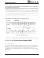
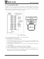
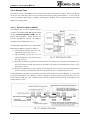
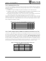
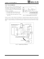
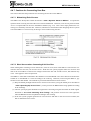
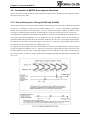
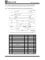
1
STD-HLS33-V6.3E Hi-speed Link System Center IC MKY33 User’s Manual Note 1. The information in this document is subject to change without prior notice. Before using this product, please confirm that this is the latest version of this document. 2. Technical information in this document, such as explanations and circuit examples, are references for this product. When actually using this product, always fully evaluate the entire system according to the design purpose based on considerations of peripheral circuits and the PC board environment. We assume no responsibility for any incompatibility between this product and your system. 3. We assume no responsibility whatsoever for any losses or damages arising from the use of the information, products, and circuits in this document, or for infringement of patents and any other rights of a third party. 4. When using this product and the information and circuits in this document, we do not guarantee the right to use any property rights, intellectual property rights, and any other rights of a third party. 5. This product is not designed for use in critical applications, such as life support systems. Contact us when considering such applications. 6. No part of this document may be copied or reproduced in any form or by any means without prior written permission from StepTechnica Co., Ltd.. MKY33 User’s Manual Preface This manual describes the MKY33, or a kind of center IC in the Hi-speed Link System. Be sure to read “Hi-speed Link System Introduction Guide” before understanding this manual and the MKY33. In this manual, the Hi-speed Link System is abbreviated as “HLS.” z Target Readers This manual is for: y Those who first build an HLS y Those who first use StepTechnica's various ICs to build an HLS z Prerequisites This manual assumes that you are familiar with: y Network technology y Semiconductor products (especially microcontrollers and memory) z Related Manuals y Hi-speed Link System Introduction Guide y Hi-speed Link System Technical Guide [Caution] y To users with “Hi-speed Link System User’s Manual” released before March, 2001 Some terms in this manual have been changed to conform to International Standards. This manual has been prepared based on Standard EnglishTM meeting the requirements of the International Organization for Standardization (ISO) and the American National Standards Institute (ANSI). This English manual is consistent with the Japanese document “STD- HLS33-V6.3J”. y Standard English is a trademark of Win Corporation. - iii - MKY33 User’s Manual - iv - MKY33 User’s Manual CONTENTS Chapter 1 Outline of MKY33 1.1 Role of MKY33 ....................................................................................................... 1-3 1.2 Procedure for Operating MKY33.......................................................................... 1-4 1.3 Features of MKY33 ................................................................................................ 1-5 Chapter 2 2.1 MKY33 Software Memory Map .......................................................................................................... 2-3 2.1.1 Occupied Area ............................................................................................................. 2-4 2.1.2 Data in Memory after Power-on.................................................................................. 2-4 2.1.3 Write Protection after Scan Started ........................................................................... 2-4 2.2 Areas for Basic HLS Functions............................................................................ 2-5 2.2.1 SCR Register................................................................................................................ 2-5 2.2.2 Do Area......................................................................................................................... 2-5 2.2.3 Di Area .......................................................................................................................... 2-5 2.3 Initialization, Start, and Operation of MKY33...................................................... 2-6 2.3.1 Initialization.................................................................................................................. 2-6 2.3.2 Start .............................................................................................................................. 2-6 2.3.2.1 Starting Scan ....................................................................................................... 2-6 2.3.2.2 Role of SCR.......................................................................................................... 2-6 2.3.2.3 Usage when FS Values Do Not Match Number of Existing Satellite ICs........ 2-7 2.3.2.4 Restrictions on Values Written to SCR and Causions..................................... 2-7 2.3.2.5 Scan time ............................................................................................................. 2-8 2.3.3 Basic Operation ........................................................................................................... 2-9 2.3.4 Stopping Scan ............................................................................................................. 2-9 2.4 User-support Functions...................................................................................... 2-10 2.4.1 Recognition of Link Status between Satellite ICs and MKY33.............................. 2-10 2.4.1.1 Control Area and Control Words ..................................................................... 2-10 2.4.1.2 Control Word ..................................................................................................... 2-11 2.4.1.3 Recognition of Link Status (1) ......................................................................... 2-11 2.4.1.4 Recognition of Link Status (2) ......................................................................... 2-12 2.4.1.5 How To Recognize Link Status between Satellite ICs and MKY33............... 2-12 2.4.2 Receiving non-Di Data (Individual Data by Expanded Functions)........................ 2-13 2.4.2.1 Relationship between Commands and Response Data Storage Areas ....... 2-13 2.4.2.2 Use of Commands 1 to 6 and Command Options.......................................... 2-14 2.4.2.3 Commands 7, 8, and F ...................................................................................... 2-14 2.4.2.4 Commands 9 to E .............................................................................................. 2-14 2.4.2.5 Detection of Request from Satellite IC ............................................................ 2-15 2.4.3 Checking Network Quality ........................................................................................ 2-16 2.4.4 Detecting Terminal Errors and Recognizing Poor Environment .......................... 2-16 - v - MKY33 User’s Manual 2.5 Notes on Accessing MKY33 ............................................................................... 2-17 2.5.1 Byte Access and Word Access ................................................................................ 2-17 2.5.2 Relationship between Response Speed and Command........................................ 2-17 2.5.3 Using Interrupt Function with SCANW Pin and SCANR Pin ................................. 2-17 2.6 Operating MKY33 for MKY34.............................................................................. 2-18 2.6.1 Operation of Do and Di Pins of MKY34 ................................................................... 2-18 2.6.2 Using Expanded Functions of MKY34..................................................................... 2-18 2.6.3 Example of Using Commands for MKY34 ............................................................... 2-19 2.6.4 Note on MKY34 Serial ID Send Function................................................................. 2-20 2.6.5 Initializing MKY33 when using battery-protected MKY34...................................... 2-20 2.7 Operating MKY33 for MKY35.............................................................................. 2-21 2.7.1 Handling of MKY35.................................................................................................... 2-21 2.7.2 Examples of Using MKY33 Di/Do Areas for MKY35 ............................................... 2-21 2.8 Operating MKY33 for MKY37.............................................................................. 2-22 2.8.1 Handling of MKY37.................................................................................................... 2-22 Chapter 3 MKY33 Hardware ................................................................................3-3 Chapter 4 Connecting MKY33 4.1 Connecting Buffer RAM........................................................................................ 4-4 4.2 Supplying Driving Clock and Hardware Reset Signal ....................................... 4-5 4.2.1 Supplying Driving Clock ............................................................................................. 4-5 4.2.2 Supplying Hardware Reset Signal ............................................................................. 4-5 4.3 Connecting Network Interface ............................................................................. 4-6 4.3.1 Selecting Communication Mode Using FH Pin......................................................... 4-6 4.3.2 RXD1 and RXD2 Pins and Two Types of Network.................................................... 4-6 4.3.3 Connecting TXE Pin and TXD Pin .............................................................................. 4-6 4.3.4 Recommended Network Connection......................................................................... 4-7 4.3.5 Setting Baud Rate........................................................................................................ 4-8 4.4 Connecting User Bus............................................................................................ 4-9 4.4.1 Data Storage Method................................................................................................... 4-9 4.4.2 Function of #SWAP Pin............................................................................................... 4-9 4.4.3 Connection to 8-bit User Bus ................................................................................... 4-10 4.4.4 Connection to 16-bit User Bus ................................................................................. 4-11 4.4.5 Recognition of Access.............................................................................................. 4-12 4.4.6 Access Time............................................................................................................... 4-13 4.4.6.1 Dynamic Arbiter in MKY33 ............................................................................... 4-13 4.4.6.2 Enable Control of Dynamic Arbiter.................................................................. 4-14 4.4.6.3 Fixing Access Time........................................................................................... 4-14 4.4.6.4 Speeding Up Access Time ............................................................................... 4-15 4.4.6.5 Details of Signal Supplied to #DAE Pin and Maximum Allowable Access Time...... 4-15 4.4.6.6 Example of Signal Supplied to #DAE Pin........................................................ 4-16 - vi - MKY33 User’s Manual 4.4.6.7 4.4.7 4.5 Use of #DAEA Pin.............................................................................................. 4-17 Cautions for Connecting User Bus.......................................................................... 4-18 4.4.7.1 Maintaining End of Access............................................................................... 4-18 4.4.7.2 Word Access when Connecting 8-bit User Bus ............................................. 4-18 Connection of MKY33 User-support Functions ............................................... 4-19 4.5.1 Pins Indicating Scan Timing (SCANR and SCANW) .............................................. 4-19 4.5.2 Output of CHK1 Pin ................................................................................................... 4-20 4.5.3 Output of CHK2 Pin ................................................................................................... 4-20 4.5.4 Output of DREQ Pin .................................................................................................. 4-20 4.6 Connection Example of MKY33 ......................................................................... 4-21 Chapter 5 Ratings 5.1 Electrical Ratings .................................................................................................. 5-3 5.2 AC Characteristics ................................................................................................ 5-4 5.2.1 Clock and Reset Timing.............................................................................................. 5-4 5.2.2 Baud Rate Timing ........................................................................................................ 5-5 5.2.3 External Baud Rate Clock (EXC) Timing ................................................................... 5-5 5.2.4 Access Timing without DAE Control when Connecting 16-bit Bus........................ 5-6 5.2.4.1 Read Timing (without DAE control when connecting 16-bit bus) .................. 5-6 5.2.4.2 Write Timing (without DAE control when connecting 16-bit bus) .................. 5-7 5.2.5 Access Timing with DAE Control when Connecting 16-bit Bus ............................. 5-8 5.2.5.1 Read Timing (with DAE control when connecting 16-bit bus) ........................ 5-8 5.2.5.2 Write Timing (with DAE control when connecting 16-bit bus) ........................ 5-9 5.2.6 Access Timing without DAE Control when Connecting 8-bit Bus........................ 5-10 5.2.6.1 Read Timing (without DAE control when connecting 8-bit bus) .................. 5-10 5.2.6.2 Write Timing (without DAE control when connecting 8-bit bus) .................. 5-11 5.2.7 Access Timing with DAE Control when Connecting 8-bit Bus ............................. 5-12 5.2.7.1 Read Timing (with DAE control when connecting 8-bit bus) ........................ 5-12 5.2.7.2 Write Timing (with DAE control when connecting 8-bit bus) ........................ 5-13 5.2.8 Buffer RAM Access Timing ...................................................................................... 5-14 5.2.9 Output Timing of CHK1, CHK2, SCANR, and SCANW ........................................... 5-14 5.3 Package Dimensions .......................................................................................... 5-15 5.4 Recommended Soldering Conditions ............................................................... 5-16 5.5 Recommended Reflow Conditions .................................................................... 5-16 Appendix Appendix 1 Memory Address Map List................................................................. App-3 Appendix 2 Scan Time Table ................................................................................. App-4 - vii - MKY33 User’s Manual Figures Fig. 1.1 Basic Operation of MKY33............................................................................... 1-4 Fig. 2.1 Details of SCR ................................................................................................... 2-6 Fig. 2.2 Position of SCAN Read Timing ....................................................................... 2-9 Fig. 2.3 Configuration of Control Word...................................................................... 2-11 Fig. 2.4 Commands Specifying Expanded Functions............................................... 2-13 Fig. 3.1 MKY33 Pin Assignment.................................................................................... 3-3 Fig. 3.2 Pin Electrical Characteristics in I/O Circuit Types of MKY33 ....................... 3-8 Fig. 4.1 BRAM Connection ............................................................................................ 4-4 Fig. 4.2 Hardware Reset................................................................................................. 4-5 Fig. 4.3 Recommended Network Connection .............................................................. 4-7 Fig. 4.4 Setting of Baud Rate by BPS0 and BPS1 Pins .............................................. 4-8 Fig. 4.5 Differences between Addresses for Byte Access Depending on Endian........ 4-9 Fig. 4.6 Connection to 8-bit User Bus ........................................................................ 4-10 Fig. 4.7 Connection to 16-bit User Bus ...................................................................... 4-11 Fig. 4.8 Output Signal of ACK Pin .............................................................................. 4-12 Fig. 4.9 MKY33 Dynamic Arbiter ................................................................................. 4-13 Fig. 4.10 Operation of Bus-Arbiter................................................................................ 4-13 Fig. 4.11 Concept of Access Time by Fixed-time Method .......................................... 4-14 Fig. 4.12 Usage Example of #DAE Pin.......................................................................... 4-16 Fig. 4.13 DAEA Equivalent Circuit in MKY33............................................................... 4-17 Fig. 4.14 Usage Example of #DAEA Pin ....................................................................... 4-17 Fig. 4.15 Maintaining End of Access ............................................................................ 4-18 Fig. 4.16 Signals Indicating Scan Timing..................................................................... 4-19 Fig. 4.17 Connection Example of MKY33..................................................................... 4-21 - viii - MKY33 User’s Manual Tables Table 2-1 Memory Map of MKY33................................................................................... 2-3 Table 2-2 Response Data Storage Areas for Commands .......................................... 2-13 Table 2-3 MKY34 Functions Selected by Commands and Data ................................ 2-18 Table 2-4 Correspondence Issued by MKY33 of MKY37 Commands....................... 2-22 Table 3-1 Pin Functions of MKY33................................................................................. 3-4 Table 3-2 Electrical Ratings of MKY33 .......................................................................... 3-7 Table 4-1 Access Time by Fixed-time Method ............................................................ 4-14 Table 4-2 Access Time when Keeping #DAE Pin High 450 ns Earlier ...................... 4-15 Table 4-3 Allowable Time Obtained from Addition of High Level Time of #DAE Pin to Access Time ........................................... 4-15 Table 5-1 Absolute Maximum Ratings........................................................................... 5-3 Table 5-2 Electrical Ratings............................................................................................ 5-3 Table 5-3 AC Characteristics Measurement Conditions.............................................. 5-4 Appendix Table 1 List of MKY33 Memory Addresses Corresponding to Satellite Addresses (SA) and Commands ................................ App-3 Appendix Table 2 Scan Time Based on FS Values and Baud Rates .................... App-4 - ix - MKY33 User’s Manual - x - Chapter 1 Outline of MKY33 This chapter describes the outline of the MKY33 in the Hi-speed Link System (HLS). 1.1 Role of MKY33................................................................................1-3 1.2 Procedure for Operating MKY33 ..................................................1-4 1.3 Features of MKY33 ........................................................................1-5 Chapter 1 Outline of MKY33 Chapter 1 Outline of MKY33 This chapter describes the outline of the MKY33 in the Hi-speed Link System (HLS). 1.1 Role of MKY33 MKY33 is a kind of center IC that constitutes the HLS. Be sure to read “Hi-speed Link System Introduction Guide” before understanding the MKY33 and this manual. Connect the MKY33 to the user CPU by using a bus connection. The MKY33 serves as memory for the user CPU. The user CPU can control all states of systems constituting the HLS by read/write access to the MKY33 (memory). The MKY33 is a center IC in the HLS released since 1993. In May 2004, the MKY36, which is an upgraded version of the MKY33, was released. StepTechnica recommends the user use the MKY36 when developing a new user system with an HLS center IC. In addition, when the user wants to use a HUB (MKY02) in the user system, the user should use the MKY36 as the HLS center IC because the MKY33 does not support the HUB (MKY02). 1-3 MKY33 User’s Manual 1.2 Procedure for Operating MKY33 The MKY33 can be operated by having read access and write access to registers and areas allocated to memory map. The operation of the MKY33 is very simple (Fig. 1.1). (1) Initialize all of the memory areas of the MKY33 connected to the memory areas of the user CPU using 00H data. (2) Write the initial data output from the I/O pin of the terminal to the Do area of the MKY33 (refer to “2.2.2 Do Area”). (3) Write the final satellite (FS) value to the system control register (SCR) of the MKY33; the HLS scan is started. (4) When the user system program references the input state of the I/O pin of the terminal, read the Di area of the MKY33 memory (refer to “2.2.3 Di Area”). (5) When the user system program changes the output state of the I/O pin of the terminal, write data to the Do area of the MKY33 memory (refer to “2.2.2 Do Area”). (6) When the user system program wants to use various user-support functions of the MKY33 memory and recognize the state of the HLS, the user system program must have read or write access to the given memory address of the MKY33 allocated to each function. Steps (1) to (3) above is equivalent to the initialization of the MKY33. Steps (4) and (5) above refer to the basic procedure for operating the MKY33. Step (6) above is the applied use of the MKY33. This applied use will certainly help the user system programmer and system engineer to effectively use the functions of the HLS for the user system. If the user system has no need to set an initial value at the output of the I/O pin of the terminal, the user can omit step (2) above. At initial start-up of the user system, the I/O pin state of the terminal is almost always at the reset default value of the satellite IC. The reset default value of the satellite IC also corresponds to “initializing all of the memory areas of the MKY33 using 00H data” in step (1) above. In most cases, the operation (in step (2) above) can be omitted. 1-4 Chapter 1 Outline of MKY33 1.3 Features of MKY33 Features of Basic Functions of MKY33 as Center IC in HLS (1) Can be connected to 8/16-bit CPU (2) Can be connected to big/little endian CPU (3) Has dynamic arbiter enabling much faster user CPU access time (4) Supports standard baud rates of 12, 6, and 3 Mbps, and baud rates via external clocks (5) Supports full- and half-duplex modes (6) Supports installation of two network types (two RXD pins) (7) Occupies 1280-byte area (from addresses 000H to 4FFH) (8) Operates on 5.0-V single power supply and available in 0.8 mm pitch, 84pins, QFP User-support Functions of MKY33 and Features (1) Can recognize link status (e.g. connection status and error occurrence) between individual satellite ICs and MKY33 (2) Can receive data on expanded functions except Di data (data on I/O input pins of each satellite IC) from individual satellite ICs (3) Can check network quality (4) Can detect terminal errors and recognize a poor operating environmental 1-5 MKY33 User’s Manual 1-6 Chapter 2 MKY33 Software This chapter describes software for using the MKY33. It assumes the environment has been created, enabling access to the MKY33 from the user system program through the connection between the user CPU and the MKY33 based on the descriptions in “Chapter 4 Connecting MKY33”. 2.1 Memory Map...................................................................................2-3 2.2 Areas for Basic HLS Functions ....................................................2-5 2.3 Initialization, Start, and Operation of MKY33 ..............................2-6 2.4 User-support Functions ..............................................................2-10 2.5 Notes on Accessing MKY33 .......................................................2-17 2.6 Operating MKY33 for MKY34 ......................................................2-18 2.7 Operating MKY33 for MKY35 ......................................................2-21 2.8 Operating MKY33 for MKY37 ......................................................2-22 Chapter 2 MKY33 Software Chapter 2 MKY33 Software This chapter describes software for using the MKY33. It assumes the environment has been created, enabling access to the MKY33 from the user system program through the connection between the user CPU and the MKY33 based on the descriptions in “Chapter 4 Connecting MKY33”. 2.1 Memory Map The areas corresponding to the registers and various functions listed in Table 2-1 are all allocated in the memory map of the MKY33. Table 2-1 Memory Map of MKY33 Address value Area name 002H to 07FH Control Area where control words corresponding to each satellite IC are arranged 080H to 0FFH Do Area for basic functions When a scan is started, data in the area from addresses 082H to 0FFH is output from the Do pin of each corresponding satellite IC 100H to 17FH Di × 180H to 1FFH C1 × 200H to 27FH C2 × 280H to 2FFH C3 × 300H to 37FH C4 × 380H to 3FFH C5 × 400H to 47FH C6 × 482H to 4FFH C7 × 500H to 7FFH Dummy 000H SCR System Control Register Register to which Final Satellite (FS) values controlling scan written 480H DREQR Data REQuest Reset Writing to this register enables the output of the DREQ pin to be reset Low. Each symbol ( , , ×, Write rights Description Area for basic functions When a scan is started, data in the Di pin of each corresponding satellite IC is stored in the area from addresses 102H to 17FH Area to store data responding to commands to be set as control words corresponding to each satellite IC For details, refer to “2.4 User-support Functions” Unused area ) in the Write Right column in the above table has the following meanings: The MKY33 memory has some areas that are write-protected when a valid FS (Final Satellite) value is written to the SCR (System Control Register) at address 000H to start scanning. Each symbol indicates the states of those areas. : This area can always be written. : Only the lower byte of the control word can be written during scanning. (Only the lower byte is written even if this area is written by word access.) : Writing to this area is ignored. × : Only read access from this area is permitted during scanning. The memory addresses of each area corresponding to Satellite Addresses (SA) are shown in “Appendix 1 Memory Address Map List”. 2-3 MKY33 User’s Manual 2.1.1 Occupied Area The MKY33 occupies the memory areas from addresses 000H to 4FFH. The area from addresses 500H to 7FFH is unused area. The MKY33 does not control the memory area from addresses 500H to 7FFH. Therefore, even if the user system program accesses this area, the output signal of the ACK pin responding to access does not change. Be careful when designing a user system that uses the output signal of the ACK pin. 2.1.2 Data in Memory after Power-on After power-on, data in the memory area from addresses 000H to 4FFH of the MKY33 is all undefined. The memory areas of the MKY33 must be initialized before using the MKY33. For details, refer to “2.3.1 Initialization”. 2.1.3 Write Protection after Scan Started After power-on, data can be read and written from and to the memory area from addresses 000H to 4FFH of the MKY33. When the user CPU starts scanning by the MKY33, the upper byte of each control word in the control area of the MKY33, the Di area, and the C1 to C7 areas for user-support functions are write-protected as indicated in the “Write Rights” column in Table 2-1. Write protection is a function for preventing the user system program from accidentally destroying read-only data in the memory area of the MKY33. However, the upper byte of the control area of the MKY33 consists only of read-only flag bits. This area is not affected even if data is written to the area by word access. 2-4 Chapter 2 MKY33 Software 2.2 Areas for Basic HLS Functions Only the System Control Register (SCR), Do area and Di area in the memory map indicated in Table 2-1 perform the basic HLS functions. Various user-support functions to use the HLS more effectively are allocated to other areas. 2.2.1 SCR Register The System Control Register (SCR) at address 000H starts scanning in the HLS. 2.2.2 Do Area The Do area from addresses 080H to 0FFH has areas covering the maximum number of connected satellite ICs (63). One word corresponds to one satellite IC. The lower 1 to 6 bits of the memory address of the Do area correspond to Satellite Address (SA). For example, when writing 135AH word data to the memory address 082H, 135AH can be set to the 16-bit I/O output pin of the satellite with “SA = 01H”. Because there is no satellite with “SA = 0”, the two bytes of the memory addresses 080H and 081H are unused RAM areas. 2.2.3 Di Area Like the Do area, the Di area from addresses 100H to 17FH has areas covering the maximum number of connected satellite ICs (63). One word corresponds to one satellite IC. The lower 1 to 6 bits of the memory address of the Di area correspond to Satellite Address (SA). For example, when reading the Di area at address 104H when the 16-bit I/O input pin of the satellite IC with “SA = 02H” is 79C4H, 79C4H data can be read, which is the same as the input pin of the terminal. Because there is no satellite with “SA = 0”, the two bytes of addresses 100H and 101H are unused RAM areas. 2-5 MKY33 User’s Manual 2.3 Initialization, Start, and Operation of MKY33 This section describes initialization, start, and basic operation of the MKY33. 2.3.1 Initialization Before turning on the MKY33, set a regulator circuits (such as DIP switches) that regulates the input level of the pin to determine communication mode (full duplex or half duplex) and baud rate. (For details, refer to “4.3.1 Selecting Communication Mode Using FH Pin”, and “4.3.5 Setting Baud Rate”.) After the MKY33 is powered on, be sure to perform the following operations: (1) Write 00H data to initialize the entire memory area (from 000H to 4FFH) in the memory map of the MKY33. (2) Write the Do output state (initial data) of the satellite IC to the Do area (from 080H to 0FFH). If the user system has no need to set an initial value to the output of the I/O pin of the terminal, the user can omit step (2) above. At the initial start-up of the user system, the I/O pin state of the terminal is almost always at the reset default value of the satellite IC. The reset default value of the satellite IC also corresponds to “Write 00H data to initialize the entire memory area of the MKY33” in step (1) above. In most cases, the operation (in step (2) above) can be omitted. 2.3.2 Start This section describes the starting MKY33. 2.3.2.1 Starting Scan The MKY33, a center IC in the HLS starts a scan when 01H to 3FH are written as Final Satellite (FS) values to bits 0 to 5 (FS0 to FS5) of the System Control Register (SCR) (Fig. 2.1). The scan is continued until the user system program writes 00H intentionally to bits 0 to 5 (FS0 to FS5) of the SCR register or until a hardware reset is activated. 2.3.2.2 Role of SCR The MKY33 scans the satellite ICs at satellite addresses up to Final Satellite (FS) values written to the SCR register, beginning with “Satellite Address (SA) = 1”. The FS values do not have to match the number of existing satellite ICs. Determine the FS values according to the purpose of the user system. If this register is read after power-on (and when no write has been executed), an undefined value is read. When a hardware reset is activated, the MKY33 recognizes “0000H” internally even if the read data is an undefined value. 2-6 Chapter 2 MKY33 Software 2.3.2.3 Usage when FS Values Do Not Match Number of Existing Satellite ICs This section describes a case where FS values written to the System Control Register (SCR) do not match the number of existing satellite ICs. z Example 1: When 20 existing satellite ICs connected, consecutive SAs beginning with “1”set, and FS value = “8 (08H)” The satellite ICs at “SA = 1” to “SA = 8” will be scanned. The satellite ICs at “SA = 9” to “SA = 20 (14H)” will not be scanned even if the satellite IC is powered on. In this case, the scan time is calculated by an equation with FS = “8”. z Example 2: When 20 existing satellite ICs connected, consecutive SAs beginning with “1”set, and FS value = “30 (1EH)” The satellite ICs at “SA = 1” to “SA = 20 (14H)” respond to a scanning and become available when the user system reads and writes data from and to each area in the memory map of the MKY33. In this case, the scan time is calculated by an equation with “FS = 30 (1EH)”. When additional 10 satellite ICs at “SA = 21 (15H)” to “SA = 30 (1EH)” are connected, they also respond to a scanning and become available when data the user system reads and writes from and to each area in the memory map of the MKY33. These examples indicate that the scan time can be speeded up to the time that the user system requires and satellite ICs can be hot-swappble. 2.3.2.4 Restrictions on Values Written to SCR and Causions The numeric values that can be written as FS values to the SCR (System Control Register) are “0 (00H)” to “63 (3FH)”. However, if full-duplex mode is selected for the MKY33, writing “1 (01H)” is protected. When writing FS values to the SCR register, always note the following points: (1) If full-duplex mode is selected for the MKY33, write any FS value greater than “3 (03H)” to the SCR register, even if only one satellite IC at “SA = 1” is connected or two existing satellite ICs at “SA = 1” and “SA = 2” are connected. (2) Writing “0 (00H)” to the SCR register causes the scan to stop. Do not write “0 (00H)” to the SCR register except when intentionally stopping the MKY33 scanning. (3) Do not write to the SCR register during scanning except when overwriting FS values or stopping scanning. 2-7 MKY33 User’s Manual 2.3.2.5 Scan time The MKY33 scan time can be calculated by equations below. These equations are determined by the following three elements including the values that the user system program writes to the System Control Register (SCR). (1) Full- or half-duplex modes (2) Final Satellite (FS) value of System Control Register (SCR) (3) Baud rate The equation for scan time in full-duplex mode 182 × FS × TBPS (s) “182” is a constant. The equation for scan time in half-duplex mode 354 × FS × TBPS (s) “354” is a constant. The scan time calculated by the above equations is shown in “Appendix 2 Scan Time Table”. 2-8 Chapter 2 MKY33 Software 2.3.3 Basic Operation The user system program can operate the satellite IC connected to MKY33 by read access or write access to each area in the memory map during scanning. For example, writing 135AH word data to the memory address 082H, the 16-bit I/O output pin of the satellite IC with “SA = 01H” comes into the 135AH state. For example, reading the Di area at address 104H when the 16-bit I/O input pin of the satellite IC with “SA = 02H” are 79C4H, user system program can read 79C4H data identical to the input pin state of the terminal. During this operation, the user system program can easily control the system like PIO (Parallel I/O), which is one of CPU resource, except the signal delay in the scan time. When the HLS is operated this way, constancy is completely maintained. This is most common usage of the HLS, and is also available for various applications. The end timing of a scan in the HLS is called “SCAN Read timing” (Fig. 2.2). The MKY33 outputs pulse signals from the SCAN Read (SCANR) pin at the SCAN Read. When the user CPU receives the interrupt triggers generated by the pulse signals from the SCANR pin, the user system program can recognize the end timing of a single scan in the HLS to execute a program. For details of the SCANR pin, refer to “4.5.1 Pins Indicating Scan Timing (SCANR and SCANW)”. 2.3.4 Stopping Scan The user system program can intentionally stop the scan by writing 00H to bits 0 to 5 (FS0 to FS5) of the SCR register. If the user system program writes 00H to the SCR register, the next command packet (CP) is not transmitted. The next scan is started from the satellite IC at the satellite address “SA = 01H”. In the MKY33, the scan stops right after a hardware reset is activated, regardless of operation by the user system program. 2-9 MKY33 User’s Manual 2.4 User-support Functions This section describes the user-support functions of the MKY33. The following areas in the memory map of the MKY33 are allocated for user-support functions. i. Control area from addresses 002H to 07FH ii. C1 to C7 areas from addresses 180H to 4FFH iii. Area to reset the output of the DREQ pin to Low level by writing to the DREQR (Data REQuest Reset) register at address 480H The user-support functions can: (1) Recognize link status (e.g. connection status and error occurrence) between individual satellite ICs and MKY33. (2) Receive data on expanded functions from individual satellite ICs in addition to Di data (data on I/O input pin of each satellite IC). (3) Check network quality. (4) Detect terminal errors and recognize a poor operating environment. 2.4.1 Recognition of Link Status between Satellite ICs and MKY33 This section describes the operation in (1) above. 2.4.1.1 Control Area and Control Words To use the expanded functions of each satellite IC, operate control words arranged in the control area from memory addresses 002H to 07FH of the MKY33. In the control area, one control words are arranged (one word per satellite IC). The lower 1 to 6 bits of the memory addresses to specify the arrangement correspond to Satellite Address (SA). For example, the memory address 006H is a control word corresponding to the satellite IC with “SA = 03H”. 2 - 10 Chapter 2 MKY33 Software 2.4.1.2 Control Word The control word in the control area is a 16-bit register. The lower bits 0 to 3 are an area to which commands are written. Bits 4 and 5 are used to set command options. The upper bits 8 to 15 are read-only flag bits indicating status. Figure 2.3 shows configuration of the control word. Bit 15 and bit 9 in the control word is fixed at “0”. Bits 7 and 6 are unused bits and remain initialized unless otherwise intentionally operated by the user system program. 2.4.1.3 Recognition of Link Status (1) If the MKY33 cannot receive any response packet (RP) from the satellite IC after scanning, the number of consecutive nonresponses is counted as “the number of consecutive nonresponse” in bits 12 to 14 in the control word. If the number of consecutive nonresponse is one or more, the bit 10 (RX-CHKl) in the control word is “1”. If the number of consecutive nonresponse is three or more, the flag bit 11 (RX-CHK2) in the control word is “1”. If the satellite IC is not connected to the network or is not turned on, the number of consecutive nonresponse is “7”, and thereby the RX-CHK1 flag bit and RX-CHK2 flag bit are “1” respectively. The number of consecutive nonresponse is not counted beyond “7” even if there are seven or more consecutive nonresponses. 2 - 11 MKY33 User’s Manual 2.4.1.4 Recognition of Link Status (2) If the MKY33 receives a response packet (RP) from the satellite IC after scanning, the number of consecutive nonrespose set to the control word, and the RX-CHK1 flag bit and RX-CHK2 flag bit are cleared to “0” respectively. In a state where the MKY33 is linked with the satellite IC correctly, the number of consecutive nonrespose, and the RX-CHKl flag bit and RX-CHK2 flag bit are always “0” respectively. The user system program can recognize the link status (i.e. connection status, errors, and existence of a newly linked satellite IC) between satellite ICs and the MKY33 by referencing the respective bits in the control words corresponding to individual satellite ICs. 2.4.1.5 How To Recognize Link Status between Satellite ICs and MKY33 Three examples of how to recognize the link status between satellite ICs and the MKY33 are given below. z Example 1: When FS value “3” set to bits 0 to 5 (FS0 to FS5) of SCR register with no satellite IC connected to MKY33 The number of consecutive nonrespose set to three control words at addresses 002H, 004H, and 006H, is counted at every scan and reaches “7”. When the upper bits in the control word are read at this time, 7CH can be read. The same applies when a satellite IC that is not turned on is connected. This enables to recognize that the MKY33 cannot be linked with the satellite ICs with “SA = 1”, “SA = 2”, and “SA = 3”. Under this condition, the Di areas at addresses 102H, 104H, and 106H are not updated. z Example 2: When FS value “5” set to bits 0 to 5 (FS0 to FS5) of SCR register with three satellite ICs connected to MKY33 with “SA = 1” to “SA = 3” The number of consecutive nonrespose set to two control words at addresses 008H and 00AH is counted at every scan and reaches “7”. If an additional satellite IC with “SA = 5” is connected at the next scan, the number of consecutive nonrespose set to the control word at address 00AH and the RX-CHKl flag bit and RX-CHK2 flag bit are cleared to “0” respectively and a new link is established between the MKY33 and the satellite IC with “SA = 5”, enabling to recognize that the HLS is operating correctly. z Example 3: When link continued between MKY33 and satellite IC The number of consecutive nonrespose set to the control word, and the RX-CHK1 flag bit and RX-CHK2 flag bit remains “0” continuously. If a link with the satellite IC suffered temporarily interference from external noise, the number of consecutive nonresposes and the RX-CHK1 flag bit are “1” only at the scan. If a user system that wants to recognize whether the Di state is always the latest, the user system can determine whether data is obtained from the latest scan or the previous scan by checking the control word when reading Di data from the Di area. 2 - 12 Chapter 2 MKY33 Software 2.4.2 Receiving non-Di Data (Individual Data by Expanded Functions) This section describes how to “(2) Receive data on expanded functions except Di data (data on I/O input pin of each satellite IC) from individual satellite ICs” in “2.4 User-support Functions”. The expanded functions of the satellite IC can be specified by setting commands to bits 0 to 3 in the control word (Fig. 2.4). If the user uses basic HLS functions operated by the procedure in “2.3 Initialization, Start, and Operation of MKY33”, command is set to “0”. 2.4.2.1 Relationship between Commands and Response Data Storage Areas When command 1 is set, response data received by response packet (RP) from the satellite IC is stored in the C1 area on the memory map. When command 2 is set, the response data received from the satellite IC is stored in the C2 area on the memory map. Table 2-2 shows the storage areas of response data for the commands. Table 2-2 Response Data Storage Areas for Commands Command Response data storage area Reference Command Response data storage area Reference 0 (0H) Di — 8 (8H) Di Note 1 (1H) C1 — 9 (9H) C1 Note 2 (2H) C2 — 10 (A H) C2 Note 3 (3H) C3 — 11 (BH) C3 Note 4 (4H) C4 — 12 (CH) C4 Note 5 (5H) C5 — 13 (DH) C5 Note 6 (6H) C6 — 14 (E H) C6 Note 7 (7H) C7 Note 15 (FH) C7 Note Note: Each command returns to “0” after command execution is completed. 2 - 13 MKY33 User’s Manual 2.4.2.2 Use of Commands 1 to 6 and Command Options If the user system program sets any of commands 1 to 6, the designated command continues to execute until the user system program rewrites. When the user system program wants to execute any of commands 1 to 6 just once and return the command immediately to 0, simultaneously set “1” to the Automatic Clear Flag (ACF) (bit 4) in the control word when setting any one of the commands 1 to 6 in the control word. Then, the command returns to command 0 and the ACF also returns to “0” after a link with the target satellite IC is established once by the designated command (, that is, after command execution is completed). The processing can automatically go round commands 0 to 6 one-by-one. When the user system program sets “1” to the Automatic Round Flag (ARF) (bit 5) in the control word, the command is updated automatically so that the processing can go round it each time the execution of the designated command for the target satellite IC is completed. When the user system program sets command 0, and then sets “1” to the ACF and ARF, the processing automatically goes round “commands 1 to 6 just once, returning to command 0” each time command execution for the target satellite IC is completed. (1) When a link with the target satellite IC is established, the ACF is cleared and the command is updated by the ARF. Therefore, if the link is incorrect, clearing and updating will be carried over to the next scan. (2) To execute any one of the commands 1 to 6 just once, the user system program must return the command to command 0 after writing the command and a link with the target satellite IC is established. This timing must be managed by the user system program. In contrast, using the ACF eliminates the need for the user system program to manage the timing. StepTechnica recommends the ACF be used to manage timing. 2.4.2.3 Commands 7, 8, and F Commands 7, 8, and F return to command 0, regardless of the setting condition of the ACF, after a link with the target satellite IC is established once (, that is, after command execution is completed). 2.4.2.4 Commands 9 to E Commands 9 to E return to command 0, regardless of the setting condition of the ACF, after a link with the target satellite IC is established once. One word of the C1 to C6 areas where response data received by response packet (RP) is stored is forcibly cleared to 0000H. For example, if data at address 2EEH is 5AC1H and BH is set to the control word at address 06EH, the control word at address 06EH is “0” and data at address 2EEH is also 0000H after a link with the satellite IC with “SA = 37H” is established once. 2 - 14 Chapter 2 MKY33 Software 2.4.2.5 Detection of Request from Satellite IC Some satellite ICs can issue a request to the center IC. In the HLS, this request is called “DREQ (Data REQuest)”. When the MKY33 detects DREQ from a satellite IC, it sets bit 8 (DREQ) in the control word corresponding to the satellite address (SA) of the satellite IC to “1”. When the MKY33 executes a command defined as an individual function of the satellite IC, the DREQ from the satellite IC is cleared. If a DREQ is generated by any satellite IC that the MKY33 is linked to, the output of DREQ pin goes High when receiving a response packet (RP) from the satellite IC generating the DREQ. The rising edge of the DREQ pin output can be used as an interrupt trigger to the user CPU. To cause the output level of DREQ pin to change from High to Low, write 00H to the DREQR at address 480H of the MKY33 using the user system program when the DREQs in the control words corresponding to all satellite ICs are cleared. 2 - 15 MKY33 User’s Manual 2.4.3 Checking Network Quality This section describes how to “check network quality” as described in item (3) of “2.4 User-support Functions”. In the HLS, when the MKY33 is activated to start scanning, the MKY33 can receive response packets (RPs) from the satellite IC while power is applied to the unit (terminal) with the satellite IC to be scanned and the network is stable. In an environment in which a correct scan has been established once, if the MKY33 cannot receive response packets (RPs) from the satellite IC (when nonresponse occurs), the cause may be one of the following: (1) The terminal was disconnected. (2) Trouble occurred with receipt or sending of packet due to environmental problems including external noise trouble. (3) The network performance limit has been reached. If the link is corrected at the next scan, item (1) above can be excluded as a cause. Monitoring nonresponse occurrences in this way, the user system can check network quality in the HLS. The MKY33 uses the control word to manage the number of consecutive nonresponse (refer to “2.4.1.3 Recognition of Link Status (1)”). The RX-CHK1 bit in the control word transits from “0” to “1” at the first nonresponse. This state is described as the “occurrence of CHECK-1”. The MKY33 has a CHK1 pin that outputs pulse signals for a given time when CHECK-1 occurs. For details of the CHK1 pin, refer to “4.5.2 Output of CHK1 Pin”. 2.4.4 Detecting Terminal Errors and Recognizing Poor Environment This section describes how to “detect terminal errors and recognize a poor operating environment” as described in item (4) of “2.4 User-support Functions”. In the HLS, if the MKY33 cannot receive a response packet (RP) correctly and continuously from a specific satellite IC (nonresponse occurs consecutively), the cause may be one of the following: (1) The terminal was disconnected. (2) The system operating environment is extremely poor. (3) The network performance limit has been reached. If a specific satellite IC continuously makes no response, it is likely that the cause is (1) “The terminal was disconnected.” above. However, if the user system does not intend to disconnect a specific terminal, a terminal error is assumed. If there is no terminal error, the likely causes are (2) “The system operating environment is extremely poor.” or (3) “The network performance limit has been reached.” above. The MKY33 uses the control word to manage the number of consecutive nonresposes (refer to “2.4.1.3 Recognition of Link Status (1)”). The RX-CHK2 bit in the control word transits from “0” to “1” when the third nonresponse occurs. This state is called the “occurrence of CHECK-2”. The MKY33 has a CHK2 pin that outputs pulse signals for a given time when CHECK-2 occurs. For details of the CHK2 pin, refer to “4.5.3 Output of CHK2 Pin”. 2 - 16 Chapter 2 MKY33 Software 2.5 Notes on Accessing MKY33 This section describes the notes for the user system program to access the MKY33. 2.5.1 Byte Access and Word Access The HLS handles data in 16-bit words. If the user system uses the MKY33 connected to the user CPU via the 8-bit bus, take care when the user system program reads or writes data consisting of more than 8 bits (9 bits or more). For details, refer to “4.4.7.2 Word Access when Connecting 8-bit User Bus”. 2.5.2 Relationship between Response Speed and Command Data set in the Do area of the MKY33 memory is sent to the satellite IC at every scan, regardless of the type of executed command. Therefore response speed remains unchanged. On the other, there is only one type of response data corresponding to one command during a scan, which is received by a response packet (RP) from the satellite IC, and in the Di area and C1 to C7 areas of the MKY33 memory. Therefore, data in the Di area is not updated at scanning by a command other than command “0”, so the apparent response speed may decrease in the user system monitoring data on the Di area. 2.5.3 Using Interrupt Function with SCANW Pin and SCANR Pin When the user CPU uses a signal output from the SCANW pin or SCANR pin described in “4.5 Connection of MKY33 User-support Functions” as a trigger causing the user CPU to change to interrupt han- dling, the user must understand an interrupt overhead time fully. For example, when the user CPU responds to an interrupt at low speed and if an interrupt is generated by the SCANR signal to read the state in which a single scan is completed, the first data in the MKY33 memory may have already been updated by the next scan. In a user system that uses such an interrupt, an appropriate interrupt overhead time should be considered. 2 - 17 MKY33 User’s Manual 2.6 Operating MKY33 for MKY34 This section describes how to operate the MKY33 for the MKY34, or a kind of satellite IC. Refer to “MKY34 User’s Manual” before understanding this section. 2.6.1 Operation of Do and Di Pins of MKY34 When operating Do and Di pins of the MKY34, the basic HLS functions, refer to “2.2 Areas for Basic HLS Functions” and operate them in the Do and Di areas. In this case, be sure to set command “0” to the control word so the expanded functions of the MKY34 described in “2.4.2 Receiving Non-Di Data (Individual Data by Expanded Functions)” cannot be specified from the center IC. 2.6.2 Using Expanded Functions of MKY34 The MKY34 has 16-bit binary up counters of 16 channels and one Serial IDentification Register (SIDR) as expanded functions in addition to Do and Di pins, the HLS basic functions. The MKY34 selects which of the function data to be embedded in a response packet (RP) to return according to a command from the center IC. Data on the expanded functions of the MKY34 can be obtained individually by using a command to specify the function of the MKY34 for the control word in the control area of the MKY33 corresponding to the SA (Satellite Address) where the MKY34 is connected (refer to “2.4.2 Receiving non-Di Data (Individual Data by Expanded Functions)”). Table 2-3 shows the correspondence of MKY34 functions selected by commands to MKY34 data obtained by the MKY33. Table 2-3 MKY34 Functions Selected by Commands and Data Command Response packet storage area Function of MKY34 MKY34 data obtained by MKY33 0 (0H) Di Obtain state of Di0 to Di15 pins State of Di0 to Di15 pins 1 (1H) C1 Obtain value of counter ch1 Four-digit hexadecimal value of counter ch1 2 (2H) C2 Obtain value of counter ch2 Four-digit hexadecimal value of counter ch2 3 (3H) C3 Obtain value of counter ch3 Four-digit hexadecimal value of counter ch3 4 (4H) C4 Obtain value of counter ch4 Four-digit hexadecimal value of counter ch4 5 (5H) C5 Obtain value of counter ch5 Four-digit hexadecimal value of counter ch5 6 (6H) C6 Obtain value of counter ch6 Four-digit hexadecimal value of counter ch6 7 (7H) C7 Obtain value of SIDR Value of SIDR (16 bits) 8 (8H) Di Obtain state of Di0 to Di15 pins State of Di0 to Di15 pins 9 (9H) C1 Reset counter ch1 to 0000H 0000H 10 (AH) C2 Reset counter ch2 to 0000H 0000H 11 (BH) C3 Reset counter ch3 to 0000H 0000H 12 (CH) C4 Reset counter ch4 to 0000H 0000H 13 (DH) C5 Reset counter ch5 to 0000H 0000H 14 (EH) C6 Reset counter ch6 to 0000H 0000H 15 (FH) C7 Obtain value of SIDR Value of SIDR (16 bits) 2 - 18 Chapter 2 MKY33 Software 2.6.3 Example of Using Commands for MKY34 z Example 1: When monitoring counter ch1 of MKY34 with “SA = 3” regularly and clearing if necessary Step 1: Usually, set command 0 to address 006H and refer to the Di area at address 106H. Step 2: Use the interval timer, etc. of the user CPU to set command 1 and the ACF to address 006H regularly. After address 006H returns to command 0, refer to address 186H of the C1 area to obtain the value of the counter ch1 of the MKY34. Step 3: Set command 9 to address 006H when clearing the counter ch1 of the MKY34. (After returning to command 0, data at address 186H of the C1 area can be recognized as 0000H as a value after clearing.) z Example 2: When always obtaining Di state of MKY34 with “SA = 3DH” and all counter values for six channels Step 1: Set “1” to the ARF in the control word at address 07AH. Step 2: After scan times of seven scans go by Step 3: The Di state of the MKY34 can be obtained by referring to address 17AH (of the Di area). The value of counter ch1 of the MKY34 can be obtained by referring to address 1FAH (of the C1 area). The value of counter ch2 of the MKY34 can be obtained by referring to address 27AH (of the C2 area). The value of counter ch3 of the MKY34 can be obtained by referring to address 2FAH (of the C3 area). The value of counter ch4 of the MKY34 can be obtained by referring to address 37AH (of the C4 area). The value of counter ch5 of the MKY34 can be obtained by referring to address 3FAH (of the C5 area). The value of counter ch6 of the MKY34 can be obtained by referring to address 47AH (of the C6 area). Step 4: Because memory corresponding to MKY34 with “SA = 3DH” is always updated, each data in “Step 3” above can be obtained continuously. z Example 3: When MKY34 with “SA = 15” issues serial ID send request Step 1: Check that the DREQ in the control word at address 01EH is “1” (detection of request). Step 2: Set command 7 to address 01EH. Step 3: After address 01EH returns to command 0, refer to address 49EH (of the C7 area) to obtain data from the Serial IDentification Register (SIDR) of the MKY34. 2 - 19 MKY33 User’s Manual 2.6.4 Note on MKY34 Serial ID Send Function The DREQ in the control word of MKY34 may become “1” after the MKY34 is turned on even when the MKY34 does not use the serial ID send function for command 7. This event is the same state as the state where a rising-edge signal is input to the SLD pin within the MKY34 due to abnormal events (including drift in power supply to power pins) after the MKY34 is turned on. If a user system needs to deal with this, terminate the serial ID send function started by the MKY34 as follows: (1) In a user system that does not use the serial ID send function of the MKY34, issue command 7 as a dummy. Also, in a user system that uses the output signals of the DREQ pin described in “4.5.4 Output of DREQ Pin”, write 00H to DREQR (Data REQuest Reset) at address 480H of the MKY33 when DREQs from all satellite ICs are cleared. (2) If “1” had been set to the DREQ in the control word when the newly linked MKY34 was recognized as described in “2.4.1 Recognition of Link Status between Satellite ICs and MKY33”, issue command 7 as a dummy. Also, in a user system that uses the output signals of the DREQ pin described in “4.5.4 Output of DREQ Pin”, write 00H to DREQR (Data REQuest Reset) at address 480H of the MKY33 when DREQs from all satellite ICs are cleared. 2.6.5 Initializing MKY33 when using battery-protected MKY34 If the user uses the MKY34 satellite IC with battery-protected, StepTechnica recommends the user recognize the state of the advanced function corresponding to each command in the MKY34 by initializing the MKY33. After operating step (2) described in “2.3.1 Initialization”, set the command in the control word corresponding to the start of the target Satellite Address (SA) to 30H. This operation can provide the values of six channels of 16-bit binary up counters staying in the MKY34 after scanning is executed seven times. If there is an MKY34 with the DREQ in the control word at “1”, issue command 7 to obtain the value of the Serial IDentification Register (SIDR) of the MKY34. 2 - 20 Chapter 2 MKY33 Software 2.7 Operating MKY33 for MKY35 This section describes how to operate the MKY33 for the MKY35, or a kind of satellite IC. Refer to “MKY35 User’s Manual” before understanding this section. 2.7.1 Handling of MKY35 From the viewpoint of the MKY33 operation system, the MKY35 satellite IC supports only the Do and Di pins, the HLS basic functions. Therefore, fix command 0 to the control word in the control area of the MKY33 corresponding to Satellite Address (SA) where MKY35 is connected. No other operations are required. If any command other than command 0 is set accidentally to the target control word where the MKY35 is connected, this will not affect the functions and operation of the MKY35. In this case, the MKY35 embeds 0000H within a response packet (RP) to return. The MKY35 has eight operation modes: IO modes 1 to 6, and PWM (Pulse Width Modulation) modes 1 and 2. MKY35 pins select these modes to set. The meanings of data set to the Do area of the MKY33 and data returned to the Di area vary according to each mode. 2.7.2 Examples of Using MKY33 Di/Do Areas for MKY35 z Example 1: When operation mode of MKY35 with “SA = 4” is IO mode 1 All the I/O pins of the MKY35 are for “inputs”. The state of 16-bit pins can be stored to the Di area at address 108H of the MKY33. Data set to the Do area at address 088H of the MKY33 has no meaning. z Example 2: When operation mode of MKY35 with “SA = 10H” is IO mode 4 The MKY35 has 16 I/O pins: 12 for “output”, and 4 for “input”. The state of I/O pins for “input” can be stored to the lower bits 0 to 3 of the Di area at address 120H of the MKY33. Bits 4 to 15 are always at “0”. Of the data to be set to the Do area at address 0A0H of the MKY33, the data of bits 0 to 3 has no meaning and the data of bits 4 to 15 are sent to the 12 I/O pins for “output”. z Example 3: When operation mode of MKY35 with “SA = 26H” is PWM mode 1 and motor speed controlled by PWM ratio The MKY35 has 16 I/O pins: 8 I/O pins are for “input” and input data can be stored to bits 0 to 7 at address 14CH (Di area) of the MKY33. The state set to bits 8 to 11 at address 0CCH (Do area) of the MKY33 is sent to the output pins. The value set to bits 0 to 5 at address 0CCH of the MKY33 indicates the PWM ratio that can be used to control the rotational speed of a motor. Bits 6 and 7 at address 0CCH of the MKY33 are used to instruct the rotation direction and stop of the motor. For details of the functions of the MKY35 for each bit at addresses in the above examples (Di area/Do area), refer to “MKY35 User’s Manual”. 2 - 21 MKY33 User’s Manual 2.8 Operating MKY33 for MKY37 This section describes how to operate the MKY33 for the MKY37, or a kind of satellite IC. Refer to “MKY37 User’s Manual” before understanding this section. 2.8.1 Handling of MKY37 From the viewpoint of the MKY33 operation system, the MKY37 satellite IC supports only the Do and Di pins, the HLS basic functions. Therefore, fix command 0 or 8 to the control word in the control area of the MKY33 corresponding to Satellite Address (SA) where MKY37 is connected. No other operations are required. Table 2-4 Correspondence Issued by MKY33 of MKY37 Commands Command Function of MKY37 Data stored in response packet Memory area in MKY33 0 (0H) Samples Di0 to Di15 pin states State of Di0 to Di15 pins Di 1 (1H) to 7 (7H) Does not sample (STB2 not output) 0000H C1 to C7 8 (8H) Samples Di0 to Di15 pin states State of Di0 to Di15 pins Di 9 (9H) to 14 (EH) Does not sample (STB2 not output) 0000H C1 to C7 If any command other than command 0 or 8 is set accidentally to the target control word where the MKY37 is connected, this will not affect the functions and operation of the MKY37. In this case, the MKY37 embeds 0000H within a response packet (RP) to return. 2 - 22 Chapter 3 MKY33 Hardware This chapter describes the MKY33 hardware, such as pin assignment, pin functions, and I/O circuit types. Chapter 3 MKY33 Hardware Chapter 3 MKY33 Hardware This chapter describes the MKY33 hardware, such as pin assignment, pin functions, and I/O circuit types. Figure 3.1 shows the MKY33 pin assignment. 3-3 MKY33 User’s Manual Table 3-1 lists the pin functions of the MKY33. Table 3-1 Pin Functions of MKY33 Pin name Pin No. Logic I/O Function UA0 to UA10 2 to 12 Positive I 11-bit address bus pins connected to user bus The UA0 pin corresponds to the LSB and the UA10 pin to the MSB. Access to the MKY33 from the user bus requires that the signals of these pins must be stabilized before the conditions for access by the #UCS, #URD, and #UWR pins are established. UD0 to UD15 13 to 16 23 to 26 17 to 20 27 to 30 Positive I/O 16-bit bidirectional data bus pins connected to user bus The UD0 pin corresponds to the LSB and the UD15 pin to the MSB. #UCS 32 Negative I Access control pin connected to user bus For read access or write access to the MKY33, set this pin Low at the right time. #URD 33 Negative I Read control pin connected to user bus To read the MKY33, set this pin Low at the right time. I Write control pin connected to user bus To write to the MKY33, set this pin Low at the right time. If this pin signal or #UCS pin signal goes High when both are Low, UD0 to UD15 bus data are input to the MKY33. O Output pin that changes from High to Low when MKY33 recognizes access from user bus and changes from Low to High when access from user bus finishes I Input pin that selects whether to reverse signal input from A0 pin in MKY33 Set this pin Low when connected to a big-endian user bus. Set this pin High or leave it open when connecting to a little-endian user bus. #UWR ACK #SWAP 34 35 36 Negative Positive Negative #DAE 37 Negative I Input pin for enable control of dynamic arbiter To operate the dynamic arbiter, input appropriate signals generated according to the user bus timing. For how to use this pin, refer to “4.4.6 Access Time”. #DAEA 38 Negative I Input pin for enable control of dynamic arbiter Set this pin Low when generating the DAE signal in the MKY33. Keep it High or leave it open when it is not used. MKY33 Hardware reset input pin Keep this pin Low for 10 or more clock right after poweron or when resetting hardware intentionally. #RST 39 Negative I MD0 to MD7 47, 45, 41 40 44, 46 48, 50 Positive I/O 8-bit bidirectional data bus that connects to buffer RAM Connect this pin to the D0 to D7 pins of buffer RAM. MA0 to MA10 49, 51, 52 54 56, 57 59, 65, 60 58, 53 Positive O 11-bit address bus that connects to buffer RAM Connect this pin to the A0 to A10 pins of buffer RAM. (Continue) 3-4 Chapter 3 MKY33 Hardware Table 3-1 Pin Functions of MKY33 (Continued) Pin name Pin No. Logic I/O Function #MRD 55 Negative O Read control output pin that connects to buffer RAM Connect this pin to the RD pin of buffer RAM. TEST 61 Positive I Be sure to connect this pin to GND (manufacturer test pin) #MWR 66 Negative O Write control output pin that connects to buffer RAM Connect this pin to the WR pin of buffer RAM. MS 67 Positive I Input pin that selects type of buffer RAM Be sure to fix this pin at High. TXD 68 Positive O Pin that sends command packet (CP) to satellite IC Connect it to a drive input pin including driver, etc. TXE 69 Positive O This pin goes High when the output signal of the TXD pin is enabled. Connect it to a gate pin including driver, etc. RXD1 70 Positive I Input pin that inputs response packet (RP) from satellite IC This pin takes precedence over the RXD2 pin when a response packet is received simultaneously. RXD2 71 Positive I Input pin that inputs response packet (RP) from satellite IC Set this pin High or leave it open when it is not used. FH 72 Positive I Input pin that selects MYK33 communication mode Keep this pin High when selecting full-duplex mode, and Low when selecting half-duplex mode. WB 74 Positive I Input pin that selects width of connected user bus Set this pin Low when connecting to an 8-bit user bus. Set this pin Low or leave it open when connecting to a 16bit user bus. Xi 75 Positive I Driving clock input pin (48 MHz recommended) BPS0 76 Positive I Input pin that selects MKY33 baud rate BPS1 77 Positive I Input pin that selects MKY33 baud rate I Clock input pin that is used as the baud rate depends on the external clock The baud rate is 1/4 of the supplied frequency, which can be up to 12.5 MHz. Set this pin High or leave it open when it is not used. O Pin that goes High when it detects DREQ generated from satellite IC detected Leave this pin open when it is not used. O Pin that outputs High-level pulse signals for a given time right after data to be sent to final satellite got in CP during single scan Leave this pin open when it is not used. O Pin that outputs High-level pulse signals for a given time right after data received from final satellite written to BRAM in single scan Leave this pin open when it is not used. EXC DREQ SCANW SCANR 78 79 80 81 Positive Positive Positive Positive (Continue) 3-5 MKY33 User’s Manual Table 3-1 Pin Functions of MKY33 (Continued) Pin name Pin No. Logic I/O Function CHK1 82 Negative O Output pin that goes High for a given time when CHECK-1 signal generated CHK2 83 Negative O Output pin that goes High for a given time when CHECK-2 signal generated VDD 22, 42, 64 73, 84 --- --- Power pin for 5.0-V supply GND 1, 21, 31 43, 62, 63 --- --- Power pin connected to 0 V Note: Pins prefixed with # are negative logic (active Low). 3-6 Chapter 3 MKY33 Hardware Table 3-2 and Figure 3.2 shows the electrical ratings of the MKY33 pins. Table 3-2 Electrical Ratings of MKY33 No I/O Name Type No I/O Name Type No (#: Negative logic) I/O Name Type No I/O Name Type -- 1 -- GND -- 22 -- VDD -- 43 -- GND -- 64 -- VDD 2 I UA0 H 23 I/O UD4 D 44 I/O MD4 E 65 O MA7 B 3 I UA1 H 24 I/O UD5 D 45 I/O MD1 E 66 I #MWR C 4 I UA2 H 25 I/O UD6 D 46 I/O MD5 E 67 I MS G 5 I UA3 H 26 I/O UD7 D 47 I/O MD0 E 68 O TXD A 6 I UA4 H 27 I/O UD12 D 48 I/O MD6 E 69 O TXE A 7 I UA5 H 28 I/O UD13 D 49 O MA0 B 70 I RXD1 G 8 I UA6 H 29 I/O UD14 D 50 O MD7 E 71 I RXD2 G G 9 I UA7 H 30 I/O UD15 D 51 O MA1 B 72 I FH 10 I UA8 H 31 -- GND -- 52 O MA2 B 73 -- VDD -- 11 I UA9 H 32 I #UCS F 53 O MA10 B 74 I WB G 12 I UA10 H 33 I #URD F 54 O MA3 B 75 I Xi H 13 I/O UD0 D 34 I #UWR F 55 O #MRD C 76 I BPS0 G 14 I/O UD1 D 35 O ACK A 56 O MA4 B 77 I BPS1 G 15 I/O UD2 D 36 I #SWAP G 57 O MA5 B 78 I EXC G 16 I/O UD3 D 37 I #DAE G 58 O MA9 B 79 O DREQ C 17 I/O UD8 D 38 I #DAEA G 59 O MA6 B 80 O SCANW C 18 I/O UD9 D 39 I #RST G 60 O MA8 B 81 O SCANR C 19 I/O UD10 D 40 I/O MD3 E 61 I TEST G 82 O CHK1 C 20 I/O UD11 D 41 I/O MD2 E 62 I GND -- 83 O CHK2 C 21 -- GND -- 42 -- VDD -- 63 -- GND -- 84 -- VDD -- 3-7 MKY33 User’s Manual 3-8 Chapter 4 Connecting MKY33 This chapter describes the pin functions and how to connect MKY33 required for the MKY33 to operate as a center IC in the HLS. It consists of the following six categories to provide a clear understanding of the pin functions and how to connect. 4.1 Connecting Buffer RAM ................................................................4-4 4.2 Supplying Driving Clock and Hardware Reset Signal................4-5 4.3 Connecting Network Interface......................................................4-6 4.4 Connecting User Bus ....................................................................4-9 4.5 Connection of MKY33 User-support Functions........................4-19 4.6 Connection Example of MKY33..................................................4-21 Chapter 4 Connecting MKY33 Chapter 4 Connecting MKY33 This chapter describes the pin functions and how to connect MKY33 required for the MKY33 to operate as a center IC in the HLS. It consists of the following six categories to provide a clear understanding of the pin functions and how to connect. (1) Connecting Buffer RAM (2) Supplying Driving Clock and Hardware Reset Signal (3) Connecting Network Interface (4) Connecting User Bus (5) Connecting MKY33 User-suppot Functions (6) Connecting Example of MKY33 When connecting the MKY33, be sure to connect the TEST pin (pin 61) to the GND pins. Be sure to connect all the VDD pins (pins 22, 42, 64, 73, 84) to the 5.0-V power supply, and all the GND pins (pins 1, 21, 31, 43, 62, 63) to the 0-V power supply. In addition, connect a capacitor of 10 V/0.1 μF (104) or more between adjacent VDD pins and GND pins. 4-3 MKY33 User’s Manual 4.1 Connecting Buffer RAM The MKY33 does not have any internal memory. Therefore, a buffer RAM (BRAM) must be placed near the MKY33. The pins of the MKY33 are assigned so that lines to connect the MKY33 and static RAM (SRAM), which serves as the BRAM, should not cross on a circuit board. Figure 4.1 shows the connection between the MKY33 and BRAM. The user should have BRAM. Use on 8-bit wide SRAM with an access speed of 20 ns or faster as BRAM. To connect BRAM, follow the following steps: (1) Fix the MS pin (pin 67) of the MKY33 at High. (2) Connect the MA0 to MA10 pins (pins 49, 51, 52, 54, 56, 57, 59, 65, 60, 58, 53) of the MKY33 to the A0 to A10 pins of the BRAM. If the memory capacity of the BRAM is large, there will be unused address input pins. Fix the unused pins at Low. (3) Connect the MD0 to MD7 pins (pins 47, 45, 41, 40, 44, 46, 48, 50) of the MKY33 to the D0 to D7 pins of the BRAM. (4) Connect the #MRD pin (pin 55) of the MKY33 to the RD pin of the BRAM. (5) Connect the #MWR pin (pin 66) of the MKY33 to the WR pin of the BRAM. (6) Fix the CS pin of the BRAM at Low. (The #MRD pin of the MKY33 is usually kept Low. The MKY33 changes the level of the #MRD pin to High to output Low-level write pulse signals from the #MWR pin only when the MKY33 writes data to the BRAM.) 4-4 Chapter 4 Connecting MKY33 4.2 Supplying Driving Clock and Hardware Reset Signal This section describes how to supply a clock that drives the MKY33 and a hardware reset signal. 4.2.1 Supplying Driving Clock Supply an oscillator-generated 48 MHz clock to the Xi pin (pin 75) of the MKY33 for driving clock in accordance with the following specifications. The MKY33 executes all operations using the clock signal supplied to the Xi pin. If a clock signal is not supplied, the user system program does not have read and write access to the MKY33 memory. (1) Usually supply a 48 MHz external clock. The upper frequency is 50 MHz, and the lower frequency is not provided. (2) Electrical characteristics of the Xi pin: VIH = min 3.5 V, VIL = max 1.5 V (3) Clock with a signal rise and fall time of 20 ns or less (4) Clock with a minimum Hi-level or Low-level time of 5 ns or more (5) Clock with jitter component of 500 ps or less (6) Frequency accuracy of 1000 ppm (±0.1%) or better 4.2.2 Supplying Hardware Reset Signal When a Low level signal is supplied to the #RST (ReSeT) pin (pin 39), the MKY33 is hardware-reset. If a period in which the Low-level signal has been supplied is less than “one clock”, the signal is ignored to prevent malfunction. To reset the MKY33 completely, the #RST pin must be kept Low for “10 or more clock” while supplying a driving clock (Fig. 4.2). The #RST pin is connected to an internal Schmitt-type input buffer, so a constant-rise-time circuit can be connected directly at power-on. Design the circuit so that a hardware reset is surely activated immediately after MKY33 power-on. 4-5 MKY33 User’s Manual 4.3 Connecting Network Interface This section describes connection of a network interface (I/F). The network I/F of the MKY33 consists of the RXD1 pin (pin 70), RXD2 pin (pin 71), TXE pin (pin 69), and TXD pin (pin 68). The MKY33 has two receiving pins (RXD1 pin and RXD2 pin), so the user system, which uses the MKY33 as the center IC of the HLS, can build two types of network cables (Fig. 4.3). 4.3.1 Selecting Communication Mode Using FH Pin When connecting the network I/F, select full-duplex or half-duplex mode using the FH pin (pin 72). When full-duplex mode selected, set the FH pin High and when half-duplex mode selected, set the FH pin Low. When connecting the TRX (driver/receiver) to the network I/F, conform to this setting. The setting of the FH pin is one of the elements determining scan time. Do not change the level of the FH pin during scanning. 4.3.2 RXD1 and RXD2 Pins and Two Types of Network In the MKY33, a response packet (RP) from the satellite IC is input to the RXD1 pin or RXD2 pin. Connect the TRX so that a serial pattern signal for the RP transmitted from the satellite IC will be input to the RXD1 pin or the RXD2 pin. The RXD1 pin or the RXD2 pin is pulled up in the MKY33. When the user system uses a single network, leave either the RXD1 pin or the RXD2 pin open or connect it to VDD or GND. In half-duplex mode, the signal output from the TXD pin of the MKY33 may be input directly to the RXD1 pin or the RXD2 pin while the MKY33 is transmitting a command packet (CP). The MKY33 is designed not to input data when the TXE pin is High when operated in half-duplex mode, so there is no problem. 4.3.3 Connecting TXE Pin and TXD Pin In the MKY33, the TXD pin outputs a serial pattern signal for a command packet (CP) transmitted to the satellite IC. If the MKY33 is set to full-duplex mode, the TXE pin is always High. If the MKY33 is set to halfduplex mode, the TXE pin is High only while the TXD pin outputs the serial pattern signal for the CP to the satellite IC. The TXD pin alternately outputs High and Low levels with a time width of “2 × TBPS” while it does not output the serial pattern signal for the CP to the satellite IC. Design the TRX connected to the MKY33 so that the enable pin of the TRX driver is activated when the TXE pin is High, thereby enabling the serial pattern signal for the command packet (CP) output from the TXD pin to be transmitted to the network. This applies to both types of network to the MKY33. 4-6 Chapter 4 Connecting MKY33 4.3.4 Recommended Network Connection Figure 4.3 shows the recommended network connection. The TRX consists of an RS485-based driver/ receiver (LSI driven at 5.0 V) and pulse transformer. Recommended network cables include Ethernet LAN cables (10BASE-T, Category 3 or higher) and shielded network cables. When operating the HLS, full-duplex mode requires two twisted-pair cables, and half-duplex requires one twisted-pair cable. Background information to help build network cable is described in “Hi-speed Link System Technical Guide”. For more information about how to select components or to get recommended components, visit our Web site at www.steptechnica.com/. 4-7 MKY33 User’s Manual 4.3.5 Setting Baud Rate The MKY33 baud rate is determined by the settings of the BPS0 pin (pin 76) and BPS1 pin (pin 77). Figure 4.4 shows the baud rates corresponding to the settings. When both the BPS0 and BPS1 pins are kept Low, the baud rate is “1/4” of the clock frequency supplied to the EXC pin (pin 78). (For example, when the clock frequency supplied to the EXC pin is 5 MHz, the baud rate is 1.25 Mbps.) The maximum clock frequency that can be supplied to the EXC pin is 12.5 MHz with a duty ratio ranging from 40% to 60% (when Xi = 50 MHz). When not supplying a clock frequency to the EXC pin, leave the EXC pin open or connect it to VDD or GND because the EXC pin is connected pull-up resistor internally. 4-8 Chapter 4 Connecting MKY33 4.4 Connecting User Bus This section describes how to connect the user CPU and access time necessary for access to the MKY33 from the user system program. In this section, the bus signals such as address and data including control signals such as chip select (CS), read (RD) and write (WR) output directly from the user CPU, are collectivelly called the “user bus”. Signals traveling via a bus driver or bus controller are also called the user bus. 4.4.1 Data Storage Method All the registers of the MKY33 are aligned on 2-byte boundaries to optimize word access with the 16-bit bus. When using byte access with the 16-bit bus, register addresses vary depending on the endian of the user bus. Figure 4.5 shows an example of reading the same register with a big-endian user bus and a little-endian user bus. When the MKY33 is connected with the 16-bit bus, StepTechnica recommends word access be used to access, except that the user system program uses byte access after it identifies differences between register addresses. 4.4.2 Function of #SWAP Pin When connecting an 8-bit user bus, the MKY33 has a function (#SWAP pin) to absorb the above address differences. When the #SWAP pin is Low, the MKY33 inverts a signal level input to the A0 pin internally recognizes the level. When the #SWAP pin is Low and an 8-bit and big-endian user bus indicates address 000H, the MKY33 recognizes “address 001H”. When the user bus indicates address 001H, the MKY33 recognizes it “address 000H”. The #SWAP pin allows the MKY33 to identify the address signal A0 of the big-endian user bus with that of the little-endian user bus. When using byte access in the MKY33 connected with a 16-bit user bus, the #SWAP pin doesn’t function due to a logic circuit, i.e. it cannot absorb the address differences caused by endian (This is because the significance of the address signal A0). In the MKY33 connected with a 16-bit bus, StepTechnica recommends word access be used to access. 4-9 MKY33 User’s Manual 4.4.3 Connection to 8-bit User Bus This section describes how to connect the MKY33 to an 8-bit user bus (Fig. 4.6). (1) Set the WB pin (pin 74) of the MKY33 Low level. (2) Connect address signals A0 to A10 of the user bus to the UA0 to UA10 pins (pins 2 to 12) of the MKY33. (3) For a big-endian user bus, keep the #SWAP pin (pin 36) Low level; for a little-endian user bus, set the #SWAP (pin 36) pin High (or leave it open). (4) Connect data signals D0 to D7 of the user bus to the UD0 to UD7 pins (pins 13 to 16 and pins 23 to 26) of the MKY33. Since the UD8 to UD15 pins (pins 17 to 20 and pins 27 to 30) of the MKY33 are unused input/output pins, connect a pull-up or a pull-down resistor of about 47 kΩ to these pins or connect to VDD or GND to prevent these pins from being input undefined levels. (5) Connect the RD signal and the WR signal of the user bus to the #URD pin (pin 33) and the #UWR pin (pin 34) of the MKY33, respectively. When the #UCS pin (pin 32) of the MKY33 is Low, the RD signal and WR signal of the user bus are activated. (6) Connect a signal that is generated in the user bus to determine the memory allocation of the MKY33, to the #UCS pin (pin 32) of the MKY33. The #UCS input pin is activated when it is Low. The area from memory addresses 000H to 4FFH of the MKY33 is occupied by the MKY33. Even if the #UCS pin is Low, the unoccupied area from memory addresses 500H to 7FFH is not accessed in the same way as when the #UCS pin is High. 4 - 10 Chapter 4 Connecting MKY33 4.4.4 Connection to 16-bit User Bus This section describes how to connect the MKY33 to a 16-bit user bus (Fig. 4.7). (1) Fix the WB pin (pin 74) of the MKY33 at High level (or leave it open). (2) Connect address signals A1 to A10 of the user bus to the UA1 to UA10 pins (pins 3 to 12) of the MKY33. The UA0 pin (pin 2) of the MKY33 is not used. The A0 pin is an input pin, and so connect a pull-up or pull-down resistor of about 47 kΩ to the A0 pin or connect to VDD or GND, or to the address signal A0 of the user bus to prevent the A0 pin from being input an undefined level. (3) The #SWAP pin (pin 36) of the MKY33 does not function in the MKY33 connected with 16-bit user bus. It is an internally pulled-up input pin, so leave the #SWAP pin open or connect it to VDD. (4) Connect data signals D0 to D15 of the user bus to the UD0 to UD15 pins (pins 13 to 20, pins 23 to 30) of the MKY33. (5) Connect the RD signal of the user bus to the #URD pin (pin 33) of the MKY33, the WR signal to the #UWR pin (pin 34). When the #CS pin (pin 32) of the MKY33 is Low, the RD and WR signals of the user bus are activated. (6) Connect a signal that the user bus generates to determine the memory allocation of the MKY33, to the #UCS pin (pin 32) of the MKY33. The #UCS input pin is activated when it is Low. The area from memory addresses 000H to 4FFH of the MKY33 is occupied by the MKY33. Even if the #UCS pin is Low, the unoccupied area from memory addresses 500H to 7FFH is not accessed in the same way as when the #UCS pin is High. 4 - 11 MKY33 User’s Manual 4.4.5 Recognition of Access The conditions for recognizing that the MKY33 is accessed from the user CPU are as follows: (1) Read: When both #UCS pin and #URD pin Low For example, when only the #URD pin is Low, read access is not started and data is not output to the data bus. (2) Write: When both #UCS pin and #UWR pin Low For example, when both the #UCS pin and #UWR pin are Low and only the #UCS pin goes High, write access is assumed to have been terminated, and data on the data bus is input. When the MKY33 recognizes the read and write accesses in (1) and (2) above, the ACK pin (pin 35) of the MKY33 changes from High to Low. The ACK pin changes from Low to High when the access from the user bus finishes (Fig. 4.8). The access from the user bus must be continued until the output signal of this ACK pin changes from Low to High. The signal output from the ACK pin can be used as a wait request signal for access to the MKY33 from the user CPU. 4 - 12 Chapter 4 Connecting MKY33 4.4.6 Access Time The time for access to the MKY33 memory from the user bus can be fixed or variable. This section details the access time, referring to the access processing and internal workings of the MKY33. A time (such as “450 ns”) defined in this section is explained, assuming that “48 MHz” clock is supplied to the Xi pin of the MKY33 for driving clock. 4.4.6.1 Dynamic Arbiter in MKY33 The MKY33 does not have internal memory. Therefore, the buffer RAM (BRAM) described in “4.1 Connecting Buffer RAM” must be placed near the MKY33. When the user bus accesses the MKY33 memory, the MKY33 mediates access to BRAM (Fig. 4.9). The bus-arbiter that selects access rights to the BRAM in the MKY33 operates as follows: (1) The bus-arbiter usually selects the communication system (Fig. 4.10 (1)). (2) The bus-arbiter selects the user bus when it recognizes access from the user bus (Fig. 4.10 (2)). (3) When the bus-arbiter recognizes access from the user bus during access from the communication system, the bus-arbiter cannot select the user bus until access from the communication system is completed (Fig. 4.10 (3)). (4) When the communication system requests access during access from the user bus, the communication system cannot get bus-arbitration until access from the user bus is completed (Fig. 4.10 (4)). As described above, the MKY33 “reads data transmitted to the satellite IC from the BRAM” or “writes data got from the satellite IC to the BRAM”, which is required for scanning, during a gap when the user bus is not accessing the MKY33. The “dynamic arbiter” consists of the bus selecting circuit on the MKY33 and communication system. 4 - 13 MKY33 User’s Manual 4.4.6.2 Enable Control of Dynamic Arbiter The MKY33 has the #DAE (Dynamic Arbiter Enable) pin (pin 37) and #DAEA (Dynamic Arbiter Enable Automatic) pin (pin 38) as input pins for enable control of the dynamic arbiter. Processing the #DAE and #DAEA pins allows the user system to operate the dynamic arbiter. Therefore, the time for the user bus to access the MKY33 varies depending on the processing of these pins. 4.4.6.3 Fixing Access Time If the #DAE pin of the MKY33 is kept Low and its #DAEA pin High, the dynamic arbiter is always enabled. In this case, the access time of the user bus is fixed at the longest time as described in step (3) in “4.4.6.1 Dynamic Arbiter in MKY33” (Fig. 4.11). And, if the access from the user bus is recognized during access from the communication system, the user bus selection is kept waiting until access from the communication system is completed. Table 4-1 indicates the access times by fixed-time method. TRO (max.) is the time required for the MKY33 to finish outputting data during a read operation. TWP (min.) is the “minimum time for which access must be continued” required during a write operation. Table 4-1 Access Time by Fixed-time Method Symbol Conditions (Xi = 48 MHz) Min. Max. Unit TRO 8-bit wide connection (WB pin = Low) --- 540 ns TRO 16-bit wide connection (WB pin = High) --- 570 ns TWP 8-bit wide connection (WB pin = Low) 540 --- ns TWP 16-bit wide connection (WB pin = High) 570 --- ns 4 - 14 Chapter 4 Connecting MKY33 4.4.6.4 Speeding Up Access Time Access time can be speeded up (reduced) by keeping the #DAEA pin of the MKY33 High and supplying a “appropriate signal generated to the user bus by the signal output from the user CPU” to the #DAE pin, for the following reasons: (1) The MKY33 recognizes the High-level input of the #DAE pin as access from the user bus. (2) The MKY33 requires “450 ns” to read data transmitted to the satellite IC from the BRAM or to write data received from the satellite IC to the BRAM, which is required for scanning. (3) By keeping the #DAE pin High for “450 ns” before the user bus accesses the MKY33, the access time of the user bus becomes shorter (state shown in Fig. 4.10 (2)) as shown in Table 4-2. If the time for the #DAE pin to be kept High immediately before access is less than “450 ns”, the value obtained from addition of this time shortage to the time in Table 4-2 is the access time. Therefore, note that access time changes when a “signal generated to the user bus by the signal output from the user CPU”, which is supplied to the #DAE pin, changes. Table 4-2 Access Time when Keeping #DAE Pin High 450 ns Earlier Symbol Conditions (Xi = 48 MHz) Min. Max. Unit TRO 8-bit wide connection (WB pin = Low) --- 90 ns TRO 16-bit wide connection (WB pin = High) --- 120 ns TWP 8-bit wide connection (WB pin = Low) 90 --- ns TWP 16-bit wide connection (WB pin = High) 120 --- ns 4.4.6.5 Details of Signal Supplied to #DAE Pin and Maximum Allowable Access Time “The time for a signal supplied to the #DAE pin to be kept High and the time for access from the user bus” and “the time obtained from addition of both (duration of the High level and the access time) at access from the user bus following the High level of the #DAE pin” described in “4.4.6.4 Speeding Up Access Time” are limited as shown in Table 4-3. If the time limit is exceeded, the MKY33 can neither read data transmitted to the satellite IC from the BRAM nor write data received from the satellite IC to the BRAM, which are required for the scanning, and the scanning pauses until the next gap occurs. The minimum time at Low level of the #DAE pin when the MKY33 recognizes that the dynamic arbiter is enabled is “100 ns”. Table 4-3 Allowable Time Obtained from Addition of High Level Time of #DAE Pin to Access Time Baud rate Full duplex Half duplex Unit 12 Mbps 15.2 29.5 μs 6 Mbps 30.4 59.0 μs 3 Mbps 60.7 118 μs EXC 182 × TBPS 354 × TBPS s 4 - 15 MKY33 User’s Manual 4.4.6.6 Example of Signal Supplied to #DAE Pin A “appropriate signal generated to the user bus by the signal output from the user CPU”, which is supplied to the #DAE pin, is “usually Low and goes High “450 ns” earlier immediately before the user bus accesses the MKY33”. In addition, the signal must not exceed the allowable time shown in Table 4-3, including the time for the user bus to access the MKY33. To generate such a signal by a signal output from the user CPU, the following signal may be used, which “goes High while the user CPU accesses memory space other than the MKY33”. (1) For example, the M1 signal or REF signal of the Z80 when the user CPU is the Z80-CPU (Fig. 4.12). (2) For example, a status signal indicating that the user bus accesses devices other than the MKY33 (such as ROM containing frequently-accessed programs). The signal that goes Low while the user bus accesses memory space other than the MKY33 depends on the user system. The user should prepare circuits to generate appropriate signals. 4 - 16 Chapter 4 Connecting MKY33 4.4.6.7 Use of #DAEA Pin Figure 4.13 shows an internal equivalent circuit with which the #DAEA pin (pin 38) of the MKY33 is associated. This circuit produces the same effect as when the #DAE pin is Low when the following conditions are established: (1) The input signal of the #DAEA pin is Low. (2) The input signal of the #UCS pin is High. (3) The input signal of the #URD pin or #UWR pin is Low. Figure 4.14 shows a usage example of the #DAEA pin. Keeping the #DAE pin High and the #DAEA Low causes this circuit to operate as if the #DAE pin goes Low when the user bus accesses devices other than the MKY33. Using the #DAEA pin can reduce the logic gate components shown by the dotted lines in Figure 4.14. 4 - 17 MKY33 User’s Manual 4.4.7 Cautions for Connecting User Bus This section describes the precautions for connecting the user bus to the MKY33. 4.4.7.1 Maintaining End of Access The MKY33 has the dynamic arbiter described in “4.4.6.1 Dynamic Arbiter in MKY33”. To operate the dynamic arbiter correctly, the end of the access must be maintained. Therefore, a non-access period of about “43 ns” is required after one access to the MKY33 finishes (Fig. 4.15). This is not a major problem for connecting to a commonly-used user bus. However, take this into consideration when designing the user system so that the MKY33 is accessed only in the logic circuit without using the CPU. 4.4.7.2 Word Access when Connecting 8-bit User Bus When reading data consisting of more than 8 bits (9 bits or more) from word address of the Di area connected to the 8-bit user bus, two accesses occur. When the user system program makes two accesses and data in the word address of the Di area changes between the first and second accesses, data hazards may occur. This applies to the write operation. The MKY33 “reads data transmitted to the satellite IC from the BRAM” and “writes data received from the satellite IC to the BRAM” in 16 bits according to the scanning. Therefore, when using the MKY33, pay attention to this data hazard. The methods to prevent the data hazard are shown below. (1) Keep the #DAE pin High from the start to end of two accesses by using the #DAE pin as described in “4.4.6.4 Speeding Up Access Time” (, which prevents the BRAM from being updated according to the scanning). (2) The user system program should first recognize the scan timing using the SCANR or SCANW signals described in “4.5.1 Pins Indicating Scan Timing”, and performs word access at the right time when the BRAM will not be updated according to the scanning. (3) If the user system program performs two word accesses and data on the two accesses watches, the data is determined to be correct. 4 - 18 Chapter 4 Connecting MKY33 4.5 Connection of MKY33 User-support Functions This section describes the pin functions and connections required to use the MKY33 user-support functions that supports the user system. 4.5.1 Pins Indicating Scan Timing (SCANR and SCANW) This section describes the functions of the SCANW (SCAN Write) pin (pin 80) and SCANR (SCAN Read) pin (pin 81). The MKY33 scans from the “Satellite Address (SA) = 1” up to Final Satellite (FS) address written to the SCR (System Control Register). The user system can recognize whether the MKY33 scans correctly by monitoring the SCANW pin and SCANR pin. It can also measure the time of a single scan. At completion of reading data transmitted to the satellite IC at the FS from the BRAM, the SCANW pin outputs a pulse signal that goes High for “2 × TXI” (approx. 82 ns at Xi = 48 MHz). If the user system uses program that updates data in the Do area to be sent to the satellite IC at every scan, a rising-edge output from the SCANW pin can be used as an interrupt trigger to the user CPU. In this way, output signal of the SCANW pin indicates the write timing of data for updating (Fig. 4.16). At completion of writing data received from the satellite IC at the FS to the BRAM, the SCANR pin outputs a pulse signal that goes High for “82 ns”. If the user system uses program that gets data in the Di area sent from the satellite IC at every scan, a rising-edge output from the SCANR pin can be used as an interrupt trigger to the user CPU. In this way, output signal of the SCANR pin indicates the read timing of the latest data (Fig. 4.16). 4 - 19 MKY33 User’s Manual 4.5.2 Output of CHK1 Pin The MKY33 has a CHK1 (CHecK-1) pin (pin 82) that outputs a pulse signal that goes High for “2 × TXI” (approx. 82 ns at Xi = 48 MHz) when the RX-CHK1 bit of the control word becomes “1” from “0” (, that is, new nonresponse from the satellite IC occurs). Monitoring the signal of the CHK1 pin enables to detect the network or environment quality and the occurrence of a link error with the satellite IC. For details of the CHK1 pin going High, refer to “2.4.3 Checking Network Quality”. Using the signal output from the CHK1 pin as an interrupt trigger to the user CPU allows the user system program to detect the occurrence of a new link error and to cope with the error. When not used, leave this pin open. The intervals when the CHK1 pin generates pulse signals may be reduced to “182 × TBPS”. When using the output of the CHK1 pin as an interrupt trigger to the user CPU, even when the interrupt is triggered frequently, check the performance of the user CPU and capability of the user program. 4.5.3 Output of CHK2 Pin The MKY33 has a CHK2 (CHecK-2) pin (pin 83) that outputs a pulse signal that goes High for “2 × TXI” (approx. 82 ns at Xi = 48 MHz) when the RX-CHK2 bit of the control word becomes “1” from “0” (, that is, when the MKY33 detects the satellite IC nonresponses occur). Monitoring the CHK2 pin signal enables to detect the satellite IC error. For details of the CHK2 pin going High, refer to “2.4.4 Detecting Terminal Errors and Recognizing Poor Environment”. Using a signal output from the CHK2 pin as an interrupt trigger to the user CPU allows the user system program to detect the occurrence of consecutive link errors and to cope with the errors. When not used, leave this pin open. The intervals when the CHK2 pin generates pulse signals may be reduced to “182 × TBPS”. When using the output of the CHK2 pin as an interrupt trigger to the user CPU, even when the interrupt is triggered frequently, check the performance of the user CPU and capability of the user program. 4.5.4 Output of DREQ Pin The output of the DREQ (Data REQuest) pin (pin 79) goes High when it detects a request issued from the satellite IC. Monitoring the signal of the DREQ pin enables to detect a request (DREQ) issued from the satellite IC. A rising-edge of this signal can be used as an interrupt trigger to the user CPU. When the user system program wants to change the output level of the DREQ pin from High to Low, write 00H to the DREQR at address 480H of the MKY33 after clearing the DREQs of the control words corresponding to all satellite ICs. (1) For details of the DREQ, refer to “2.4.2.5 Detection of Request from Satellite IC”. (2) If 00H is written to address 480H of the MKY33 with the DREQs of all control words not cleared, the signal of the DREQ pin once goes Low and then goes High immediately. 4 - 20 Chapter 4 Connecting MKY33 4.6 Connection Example of MKY33 Figure 4.17 shows an example of the MKY33 connected to a 16-bit user bus. It shows the connection in both full- and half-duplex modes. The baud rate is 6 Mbps. The pins of user-support function are left open. 4 - 21 MKY33 User’s Manual 4 - 22 Chapter 5 Ratings This chapter describes the ratings of the MKY33. 5.1 Electrical Ratings ..........................................................................5-3 5.2 AC Characteristics ........................................................................5-4 5.3 Package Dimensions...................................................................5-15 5.4 Recommended Soldering Conditions .......................................5-16 5.5 Recommended Reflow Conditions ............................................5-16 Chapter 5 Ratings Chapter 5 Ratings This chapter describes the ratings of the MKY33. 5.1 Electrical Ratings Table 5-1 lists the absolute maximum ratings of the MKY33. Table 5-1 Absolute Maximum Ratings (Vss = 0 V) Parameter Symbol Rating Unit Power supply voltage VDD -0.3 to +7.0 V Input voltage Vi Vss-0.3 to +6.0 V Output voltage Vo Vss-0.3 to +6.0 V Peak output current (Other than Type A and D) Iop Peak ±20 mA Peak output current (Type A and D) Iop Peak ±40 mA Allowable power dissipation PT 570 mW Operating temperature Topr -40 to +85 °C Storage temperature Tstg -65 to +150 °C Table 5-2 lists the electrical ratings of the MKY33. Table 5-2 Electrical Ratings Parameter Symbol Operating power supply voltage VDD Mean operating current VDDA External input frequency Fclk Input pin capacitance Ci Conditions (TA = 25°C Vss = 0 V) Min. Typ. Max. Unit 4.5 5.0 5.5 V Vi = VDD or Vss f = 50 MHz output open --- 40 80 mA Input to Xi pin --- 48 50 MHz --- 7 15 pF --- 7 15 pF VDD = Vi = 0 V f = 1 MHz TA = 25°C Output pin capacitance Co I/O pin capacitance Ci/o --- 7 15 pF Rise/fall time of input signal TIRF --- --- 100 ns Rise/fall time of input signal TIRF --- --- 50 ms Schmitt trigger input 5-3 MKY33 User’s Manual 5.2 AC Characteristics Table 5-3 lists the measurement conditions for AC characteristics of the MKY33. Table 5-3 AC Characteristics Measurement Conditions Symbol Name Value Unit COL Output load capacitance 85 pF VDD Power supply voltage 5.0 V TA Temperature 25 °C 5.2.1 Clock and Reset Timing Symbol Name Min. Typ. Max. Unit TXI Clock period width 20 20.83 (48 Hz) --- ns TXIH Clock High level width 5 ≈10.4 --- ns TXIL Clock Low level width 5 ≈10.4 --- ns TRST Reset enable Low level width 10 × TXI --- --- ns 5-4 Chapter 5 Ratings 5.2.2 Baud Rate Timing Symbol TBPS Baud rate Short pulse width of sending signal Unit 12 Mbps (Xi = 48 MHz) ≈83.33±5 ns 6 Mbps (Xi = 48 MHz) ≈166.67±5 ns 3 Mbps (Xi = 48 MHz) ≈333.33±5 ns Symbol Name Min. Typ. Max. Remarks TTXEH Period in which TXE pin goes High (142 × TBPS) -5ns 142 × TBPS (142 × TBPS) +5ns Always High when full duplex selected TRNW Short pulse width of input signal 0.51 × TBPS 1.0 × TBPS 1.49 × TBPS Allowable pulse width as RZ signal TRWW Long pulse width of input signal 1.51 × TBPS 2.0 × TBPS 2.49 × TBPS Allowable pulse width as RZ signal 5.2.3 External Baud Rate Clock (EXC) Timing Symbol Name Min. Max. Unit TEXC External baud rate clock period width 4 × TXI --- ns TEXCH External baud rate clock High level width 1.5 × TXI --- ns TEXCL External baud rate clock Low level width 1.5 × TXI --- ns 5-5 MKY33 User’s Manual 5.2.4 Access Timing without DAE Control when Connecting 16-bit Bus This section describes the access timing without DAE control when connecting a 16-bit bus. 5.2.4.1 Read Timing (without DAE control when connecting 16-bit bus) (Xi = 48 MHz) Symbol Name Min. Max. Unit TBCS Bus change setup 50 --- ns TBCH Bus change hold 0 --- ns TDAES DAE Setup 100 --- ns TDAED DAE delay 30 --- ns TADS Address setup 0 --- ns TADH Address hold 0 --- ns TAA Access to access 2 × TXI --- ns TRA Read access TACK 182 × TBPS (Full) 354 × TBPS (Half) ns TRO Read to out (bus drive) 20 --- ns TRD Read to data (valid data output) 120 570 ns TRH Read data hold 3 --- ns TBR Bus release --- 25 ns TAD Acknowledge delay --- 25 ns TACK Acknowledge enable --- 595 ns TOA Acknowledge margin 25 --- ns 5-6 Chapter 5 Ratings 5.2.4.2 Write Timing (without DAE control when connecting 16-bit bus) (Xi = 48 MHz) Symbol Name Min. Max. Unit TBCS Bus change setup 50 --- ns TBCH Bus change hold 0 --- ns TDAES DAE Setup 100 --- ns TDAED DAE delay 30 --- ns TADS Address setup 0 --- ns TADH Address hold 0 --- ns TAA Access to access 2 × TXI --- ns TWA Write access TACK 182 × TBPS (Full) 354 × TBPS (Half) ns TWS Write data setup 5 --- ns TWH Write data hold 0 --- ns TAD Acknowledge delay --- 25 ns TACK Acknowledge enable --- 570 ns 5-7 MKY33 User’s Manual 5.2.5 Access Timing with DAE Control when Connecting 16-bit Bus This section describes the access timing with DAE control when connecting the 16-bit bus. 5.2.5.1 Read Timing (with DAE control when connecting 16-bit bus) (Xi = 48 MHz) Symbol Name Min. Max. Unit TBCS Bus change setup 50 --- ns TBCH Bus change hold 0 --- ns TDAES DAE Setup 450 --- ns TDAED DAE delay 30 --- ns TADS Address setup 0 --- ns TADH Address hold 0 --- ns TAA Access to access 2 × TXI --- ns TIAD Internal access disable --- 182 × TBPS (Full) 354 × TBPS (Half) ns TRA Read access 120 --- ns TRO Read to out (bus drive) 20 --- ns TRD Read to data (valid data output) --- 120 ns TRH Read data hold 3 --- ns TBR Bus release --- 25 ns TAD Acknowledge delay --- 25 ns TACK Acknowledge enable --- 145 ns TOA Acknowledge margin 25 --- ns 5-8 Chapter 5 Ratings 5.2.5.2 Write Timing (with DAE control when connecting 16-bit bus) (Xi = 48 MHz) Symbol Name Min. Max. Unit TBCS Bus change setup 100 --- ns TBCH Bus change hold 0 --- ns TDAES DAE Setup 450 --- ns TDAED DAE delay 30 --- ns TADS Address setup 0 --- ns TADH Address hold 0 --- ns TAA Access to access 2 × TXI --- ns TIAD Internal access disable --- 182 × TBPS (Full) 354 × TBPS (Half) ns TWA Write access 120 --- ns TWS Write data setup 5 --- ns TWH Write data hold 0 --- ns TAD Acknowledge delay --- 25 ns TACK Acknowledge enable --- 140 ns 5-9 MKY33 User’s Manual 5.2.6 Access Timing without DAE Control when Connecting 8-bit Bus This section describes the access timing without DAE control when connecting a 8-bit bus. 5.2.6.1 Read Timing (without DAE control when connecting 8-bit bus) (Xi = 48 MHz) Symbol Name Min. Max. Unit TBCS Bus change setup 50 --- ns TBCH Bus change hold 0 --- ns TDAES DAE Setup 100 --- ns TDAED DAE delay 30 --- ns TADS Address setup 0 --- ns TADH Address hold 0 --- ns TAA Access to access 2 × TXI --- ns TRA Read access TACK 182 × TBPS (Full) 354 × TBPS (Half) ns TRO Read to out (bus drive) 20 --- ns TRD Read to data (valid data output) 90 540 ns TRH Read data hold 3 --- ns TBR Bus release --- 25 ns TAD Acknowledge delay --- 25 ns TACK Acknowledge enable --- 565 ns TOA Acknowledge margin 25 --- ns 5 - 10 Chapter 5 Ratings 5.2.6.2 Write Timing (without DAE control when connecting 8-bit bus) (Xi = 48 MHz) Symbol Name Min. Max. Unit TBCS Bus change setup 50 --- ns TBCH Bus change hold 0 --- ns TDAES DAE Setup 100 --- ns TDAED DAE delay 30 --- ns TADS Address setup 0 --- ns TADH Address hold 0 --- ns TAA Access to access 2 × TXI --- ns TWA Write access TACK 182 × TBPS (Full) 354 × TBPS (Half) ns TWS Write data setup 5 --- ns TWH Write data hold 0 --- ns TAD Acknowledge delay --- 25 ns TACK Acknowledge enable --- 540 ns 5 - 11 MKY33 User’s Manual 5.2.7 Access Timing with DAE Control when Connecting 8-bit Bus This section describes the access timing with DAE control when connecting the 8-bit bus. 5.2.7.1 Read Timing (with DAE control when connecting 8-bit bus) (Xi = 48 MHz) Symbol Name Min. Max. Unit TBCS Bus change setup 50 --- ns TBCH Bus change hold 0 --- ns TDAES DAE Setup 450 --- ns TDAED DAE delay 30 --- ns TADS Address setup 0 --- ns TADH Address hold 0 --- ns TAA Access to access 2 × TXI --- ns TIAD Internal access disable --- 182 × TBPS (Full) 354 × TBPS (Half) ns TRA Read access 90 --- ns TRO Read to out (bus drive) 20 --- ns TRD Read to data (valid data output) --- 90 ns TRH Read data hold 3 --- ns TBR Bus release --- 25 ns TAD Acknowledge delay --- 25 ns TACK Acknowledge enable --- 115 ns TOA Acknowledge margin 25 --- ns 5 - 12 Chapter 5 Ratings 5.2.7.2 Write Timing (with DAE control when connecting 8-bit bus) (Xi = 48 MHz) Symbol Name Min. Max. Unit TBCS Bus change setup 100 --- ns TBCH Bus change hold 0 --- ns TDAES DAE Setup 450 --- ns TDAED DAE delay 30 --- ns TADS Address setup 0 --- ns TADH Address hold 0 --- ns TAA Access to access 2 × TXI --- ns TIAD Internal access disable --- 182 × TBPS (Full) 354 × TBPS (Half) ns TWA Write access 90 --- ns TWS Write data setup 5 --- ns TWH Write data hold 0 --- ns TAD Acknowledge delay --- 25 ns TACK Acknowledge enable --- 110 ns 5 - 13 MKY33 User’s Manual 5.2.8 Buffer RAM Access Timing (Xi = 48 MHz) Symbol Name Min. Max. Unit TMAR Memory read access 20 --- ns TMRW Read to write 20 --- ns TMWR Write to read 20 --- ns TMWP Write pulse 20 --- ns TMS Address data setup 10 --- ns TMH Address data hold 10 --- ns 5.2.9 Output Timing of CHK1, CHK2, SCANR, and SCANW Symbol Name Min. Typ. Max. Unit TTRG High-level pulse width (2 × TXI) - 3 2 × TXI (2 × TXI) + 3 ns TPTP1 Pulse to pulse 1 4 × TXI --- --- ns TPTP2 Pulse to pulse 2 364 × TBPS (Full) 354 × TBPS (Half) 364 × TBPS × (FS±1) (Full) 354 × TBPS × (FS±1) (Half) --- ns 5 - 14 Chapter 5 Ratings 5.3 Package Dimensions The current release of MKY33 package is “MKY33A”, indicating a bug-fixed, improved version from the released product in earlier stages of development. 5 - 15 MKY33 User’s Manual 5.4 Recommended Soldering Conditions Parameter Symbol Reflow Manual soldering iron Temp. Peak temperature (resin surface) Tp 260°C max. 350°C max. Peak temperature holding time tp 10 s max. 3 s max. (1) Product storage conditions: TA = 30°C max., RH = 70% for prevention of moisture absorption (2) Manual soldering: Temperature of the tip of soldering iron 350°C, 3 s max. (Device lead temperature 270°C, 10 s max.) (3) Reflow: Twice max. (4) Flux: Non-chlorine flux (should be cleaned sufficiently) (5) Ultrasonic cleaning: Depending on frequencies and circuit board shapes, ultrasonic cleaning may cause resonance, affecting lead strength 5.5 Recommended Reflow Conditions Parameter Symbol Value Pre-heat (time) t1 60 to 120/s Pre-heat (temperature) T1 150 to 180°C Temperature rise rate a 2°C to 5°C/s Peak condition (time) tp 10 ±3 s max. Peak condition (temperature) Tp 255 + 5°C Cooling rate b 2 to 5°C/s High temperature area tw 220°C, 60 s max. Removal temperature T2 ≤ 100°C The recommended conditions apply to hot-air reflow or infrared reflow. Temperature indicates resin surface temperature of the package. 5 - 16 Appendix Appendix 1 Memory Address Map List........................................App-3 Appendix 2 Scan Time Table ........................................................App-4 Appendix Appendix Appendix 1 Memory Address Map List Appendix Table 1 List of MKY33 Memory Addresses Corresponding to Satellite Addresses (SA) and Commands SA Control Do Di C1 C2 C3 C4 C5 C6 C7 1 (01H) 2 (02H) 3 (03H) 4 (04H) 5 (05H) 6 (06H) 7 (07H) 8 (08H) 9 (09H) 10 (0AH) 11 (0BH) 12 (0CH) 13 (0DH) 14 (0EH) 15 (0FH) 16 (10H) 17 (11H) 18 (12H) 19 (13H) 20 (14H) 21 (15H) 22 (16H) 23 (17H) 24 (18H) 25 (19H) 26 (1AH) 27 (1BH) 28 (1CH) 29 (1DH) 30 (1EH) 31 (1FH) 32 (20H) 33 (21H) 34 (22H) 35 (23H) 36 (24H) 37 (25H) 38 (26H) 39 (27H) 40 (28H) 41 (29H) 42 (2AH) 43 (2BH) 44 (2CH) 45 (2DH) 46 (2EH) 47 (2FH) 48 (30H) 49 (31H) 50 (32H) 51 (33H) 52 (34H) 53 (35H) 54 (36H) 55 (37H) 56 (38H) 57 (39H) 58 (3AH) 59 (3BH) 60 (3CH) 61 (3DH) 62 (3EH) 63 (3FH) 002 004 006 008 00A 00C 00E 010 012 014 016 018 01A 01C 01E 020 022 024 026 028 02A 02C 02E 030 032 034 036 038 03A 03C 03E 040 042 044 046 048 04A 04C 04E 050 052 054 056 058 05A 05C 05E 060 062 064 066 068 06A 06C 06E 070 072 074 076 078 07A 07C 07E 082 084 086 088 08A 08C 08E 090 092 094 096 098 09A 09C 09E 0A0 0A2 0A4 0A6 0A8 0AA 0AC 0AE 0B0 0B2 0B4 0B6 0B8 0BA 0BC 0BE 0C0 0C2 0C4 0C6 0C8 0CA 0CC 0CE 0D0 0D2 0D4 0D6 0D8 0DA 0DC 0DE 0E0 0E2 0E4 0E6 0E8 0EA 0EC 0EE 0F0 0F2 0F4 0F6 0F8 0FA 0FC 0FE 102 104 106 108 10A 10C 10E 110 112 114 116 118 11A 11C 11E 120 122 124 126 128 12A 12C 12E 130 132 134 136 138 13A 13C 13E 140 142 144 146 148 14A 14C 14E 150 152 154 156 158 15A 15C 15E 160 162 164 166 168 16A 16C 16E 170 172 174 176 178 17A 17C 17E 182 184 186 188 18A 18C 18E 190 192 194 196 198 19A 19C 19E 1A0 1A2 1A4 1A6 1A8 1AA 1AC 1AE 1B0 1B2 1B4 1B6 1B8 1BA 1BC 1BE 1C0 1C2 1C4 1C6 1C8 1CA 1CC 1CE 1D0 1D2 1D4 1D6 1D8 1DA 1DC 1DE 1E0 1E2 1E4 1E6 1E8 1EA 1EC 1EE 1F0 1F2 1F4 1F6 1F8 1FA 1FC 1FE 202 204 206 208 20A 20C 20E 210 212 214 216 218 21A 21C 21E 220 222 224 226 228 22A 22C 22E 230 232 234 236 238 23A 23C 23E 240 242 244 246 248 24A 24C 24E 250 252 254 256 258 25A 25C 25E 260 262 264 266 268 26A 26C 26E 270 272 274 276 278 27A 27C 27E 282 284 286 288 28A 28C 28E 290 292 294 296 298 29A 29C 29E 2A0 2A2 2A4 2A6 2A8 2AA 2AC 2AE 2B0 2B2 2B4 2B6 2B8 2BA 2BC 2BE 2C0 2C2 2C4 2C6 2C8 2CA 2CC 2CE 2D0 2D2 2D4 2D6 2D8 2DA 2DC 2DE 2E0 2E2 2E4 2E6 2E8 2EA 2EC 2EE 2F0 2F2 2F4 2F6 2F8 2FA 2FC 2FE 302 304 306 308 30A 30C 30E 310 312 314 316 318 31A 31C 31E 320 322 324 326 328 32A 32C 32E 330 332 334 336 338 33A 33C 33E 340 342 344 346 348 34A 34C 34E 350 352 354 356 358 35A 35C 35E 360 362 364 366 368 36A 36C 36E 370 372 374 376 378 37A 37C 37E 382 384 386 388 38A 38C 38E 390 392 394 396 398 39A 39C 39E 3A0 3A2 3A4 3A6 3A8 3AA 3AC 3AE 3B0 3B2 3B4 3B6 3B8 3BA 3BC 3BE 3C0 3C2 3C4 3C6 3C8 3CA 3CC 3CE 3D0 3D2 3D4 3D6 3D8 3DA 3DC 3DE 3E0 3E2 3E4 3E6 3E8 3EA 3EC 3EE 3F0 3F2 3F4 3F6 3F8 3FA 3FC 3FE 402 404 406 408 40A 40C 40E 410 412 414 416 418 41A 41C 41E 420 422 424 426 428 42A 42C 42E 430 432 434 436 438 43A 43C 43E 440 442 444 446 448 44A 44C 44E 450 452 454 456 458 45A 45C 45E 460 462 464 466 468 46A 46C 46E 470 472 474 476 478 47A 47C 47E 482 484 486 488 48A 48C 48E 490 492 494 496 498 49A 49C 49E 4A0 4A2 4A4 4A6 4A8 4AA 4AC 4AE 4B0 4B2 4B4 4B6 4B8 4BA 4BC 4BE 4C0 4C2 4C4 4C6 4C8 4CA 4CC 4CE 4D0 4D2 4D4 4D6 4D8 4DA 4DC 4DE 4E0 4E2 4E4 4E6 4E8 4EA 4EC 4EE 4F0 4F2 4F4 4F6 4F8 4FA 4FC 4FE App - 3 MKY33 User’s Manual Appendix 2 Scan Time Table Appendix Table 2 Scan Time Based on FS Values and Baud Rates (Unit: μs) 12 Mbps FS Value 1 (01H) 2 (02H) 3 (03H) 4 (04H) 5 (05H) 6 (06H) 7 (07H) 8 (08H) 9 (09H) 10 (0AH) 11 (0BH) 12 (0CH) 13 (0DH) 14 (0EH) 15 (0FH) 16 (10H) 17 (11H) 18 (12H) 19 (13H) 20 (14H) 21 (15H) 22 (16H) 23 (17H) 24 (18H) 25 (19H) 26 (1AH) 27 (1BH) 28 (1CH) 29 (1DH) 30 (1EH) 31 (1FH) 32 (20H) 33 (21H) 34 (22H) 35 (23H) 36 (24H) 37 (25H) 38 (26H) 39 (27H) 40 (28H) 41 (29H) 42 (2AH) 43 (2BH) 44 (2CH) 45 (2DH) 46 (2EH) 47 (2FH) 48 (30H) 49 (31H) 50 (32H) 51 (33H) 52 (34H) 53 (35H) 54 (36H) 55 (37H) 56 (38H) 57 (39H) 58 (3AH) 59 (3BH) 60 (3CH) 61 (3DH) 62 (3EH) 63 (3FH) FULL ------------45.50 60.67 75.83 91.00 106.17 121.33 136.50 151.67 166.83 182.00 197.17 212.33 227.50 242.67 257.83 273.00 288.17 303.33 318.50 333.67 348.83 364.00 379.17 394.33 409.50 424.67 439.83 455.00 470.17 485.33 500.50 515.67 530.83 546.00 561.17 576.33 591.50 606.67 621.83 637.00 652.17 667.33 682.50 697.67 712.83 728.00 743.17 758.33 773.50 788.67 803.83 819.00 834.17 849.33 864.50 879.67 894.83 910.00 925.17 940.33 955.50 HALF 29.50 59.00 88.50 118.00 147.50 177.00 206.50 236.00 265.50 295.00 324.50 354.00 383.50 413.00 442.50 472.00 501.50 531.00 560.50 590.00 619.50 649.00 678.50 708.00 737.50 767.00 796.50 826.00 855.50 885.00 914.50 944.00 973.50 1,003.00 1,032.50 1,062.00 1,091.50 1,121.00 1,150.50 1,180.00 1,209.50 1,239.00 1,268.50 1,298.00 1,327.50 1,357.00 1,386.50 1,416.00 1,445.50 1,475.00 1,504.50 1,534.00 1,563.50 1,593.00 1,622.50 1,652.00 1,681.50 1,711.00 1,740.50 1,770.00 1,799.50 1,829.00 1,858.50 6 Mbps FULL ------------91.00 121.33 151.67 182.00 212.33 242.67 273.00 303.33 333.67 364.00 394.33 424.67 455.00 485.33 515.67 546.00 576.33 606.67 637.00 667.33 697.67 728.00 758.33 788.67 819.00 849.33 879.67 910.00 940.33 970.67 1,001.00 1,031.33 1,061.67 1,092.00 1,122.33 1,152.67 1,183.00 1,213.33 1,243.67 1,274.00 1,304.33 1,334.67 1,365.00 1,395.33 1,425.67 1,456.00 1,486.33 1,516.67 1,547.00 1,577.33 1,607.67 1,638.00 1,668.33 1,698.67 1,729.00 1,759.33 1,789.67 1,820.00 1,850.33 1,880.67 1,911.00 App - 4 HALF 59.00 118.00 177.00 236.00 295.00 354.00 413.00 472.00 531.00 590.00 649.00 708.00 767.00 826.00 885.00 944.00 1,003.00 1,062.00 1,121.00 1,180.00 1,239.00 1,298.00 1,357.00 1,416.00 1,475.00 1,534.00 1,593.00 1,652.00 1,711.00 1,770.00 1,829.00 1,888.00 1,947.00 2,006.00 2,065.00 2,124.00 2,183.00 2,242.00 2,301.00 2,360.00 2,419.00 2,478.00 2,537.00 2,596.00 2,655.00 2,714.00 2,773.00 2,832.00 2,891.00 2,950.00 3,009.00 3,068.00 3,127.00 3,186.00 3,245.00 3,304.00 3,363.00 3,422.00 3,481.00 3,540.00 3,599.00 3,658.00 3,717.00 3 Mbps FULL ------------182.00 242.67 303.33 364.00 424.67 485.33 546.00 606.67 667.33 728.00 788.67 849.33 910.00 970.67 1,031.33 1,092.00 1,152.67 1,213.33 1,274.00 1,334.67 1,395.33 1,456.00 1,516.67 1,577.33 1,638.00 1,698.67 1,759.33 1,820.00 1,880.67 1,941.33 2,002.00 2,062.67 2,123.33 2,184.00 2,244.67 2,305.33 2,366.00 2,426.67 2,487.33 2,548.00 2,608.67 2,669.33 2,730.00 2,790.67 2,851.33 2,912.00 2,972.67 3,033.33 3,094.00 3,154.67 3,215.33 3,276.00 3,336.67 3,397.33 3,458.00 3,518.67 3,579.33 3,640.00 3,700.67 3,761.33 3,822.00 HALF 118.00 236.00 354.00 472.00 590.00 708.00 826.00 944.00 1,062.00 1,180.00 1,298.00 1,416.00 1,534.00 1,652.00 1,770.00 1,888.00 2,006.00 2,124.00 2,242.00 2,360.00 2,478.00 2,596.00 2,714.00 2,832.00 2,950.00 3,068.00 3,186.00 3,304.00 3,422.00 3,540.00 3,658.00 3,776.00 3,894.00 4,012.00 4,130.00 4,248.00 4,366.00 4,484.00 4,602.00 4,720.00 4,838.00 4,956.00 5,074.00 5,192.00 5,310.00 5,428.00 5,546.00 5,664.00 5,782.00 5,900.00 6,018.00 6,136.00 6,254.00 6,372.00 6,490.00 6,608.00 6,726.00 6,844.00 6,962.00 7,080.00 7,198.00 7,316.00 7,434.00 Appendix App - 5 North America Distributor Trans Data Technologies, Inc. 340 Arthur Ave. Roselle, IL 60172 Telephone: 630-440-4075 Facsimile: 630-539-4475 e-mail: [email protected] http://www.steptechnica.us/ Developed and manufactured by StepTechnica Co., Ltd. 757-3, Shimo-fujisawa, Iruma-shi, Saitama 358-0011 TEL: 04-2964-8804 FAX: 04-2964-7653 http://www.steptechnica.com/ [email protected] Hi-speed Link System Center IC MKY33 User’s Manual Document No.: STD-HLS33-V6.3E Issued: April 2009