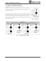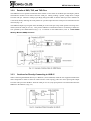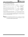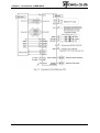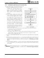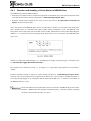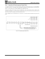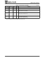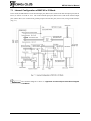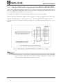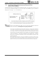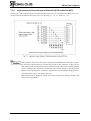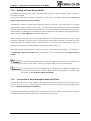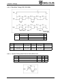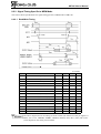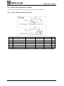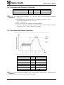
1
STD-CU40-V2.4E CUnet CUnet IC MKY40 User’s Manual Note 1. The information in this document is subject to change without prior notice. Before using this product, please confirm that this is the latest version of this document. 2. Technical information in this document, such as explanations and circuit examples, are references for this product. When actually using this product, always fully evaluate the entire system according to the design purpose based on considerations of peripheral circuits and the PC board environment. We assume no responsibility for any incompatibility between this product and your system. 3. We assume no responsibility whatsoever for any losses or damages arising from the use of the information, products, and circuits in this document, or for infringement of patents and any other rights of a third party. 4. When using this product and the information and circuits in this document, we do not guarantee the right to use any property rights, intellectual property rights, and any other rights of a third party. 5. This product is not designed for use in critical applications, such as life support systems. Contact us when considering such applications. 6. No part of this document may be copied or reproduced in any form or by any means without prior written permission from StepTechnica Co., Ltd.. MKY40 User’s Manual Preface This manual describes the MKY40, or a kind of CUnet IC. Be sure to read “CUnet Introduction Guide” before understanding this manual and the MKY40. z Target Readers This manual is for: y Those who first build a CUnet y Those who first use StepTechnica's various ICs to build a CUnet z Prerequisites This manual assumes that you are familiar with: y Network technology y Semiconductor products (especially microcontrollers and memory) z Related Manuals y CUnet Introduction Guide y CUnet Technical Guide [Caution] y To users with “CUnet User’s Manual” released before March, 2001 Some terms in this manual have been changed to conform to International Standards. y Some terms in this manual are different from those used on our website and in our product brochures. The brochure uses ordinary terms to help many people in various industries understand our products. Please understand technical information on HLS Family and CUnet Family based on technical documents (manuals). This manual has been prepared based on Standard EnglishTM meeting the requirements of the International Organization for Standardization (ISO) and the American National Standards Institute (ANSI). This English manual is consistent with the Japanese document “STD-CU40V2.4J”. y Standard English is a trademark of Win Corporation. - iii - MKY40 User’s Manual - iv - MKY40 User’s Manual CONTENTS Chapter 1 MKY40 Role and Features 1.1 CUnet Station in MEM Mode (MEM Station)....................................................... 1-3 1.2 Features of MEM Mode ......................................................................................... 1-4 1.3 Station in IO Mode (I/O Station) ........................................................................... 1-5 1.4 Features of IO Mode.............................................................................................. 1-6 1.5 Mode Selection ...................................................................................................... 1-6 Chapter 2 Hardware in MEM Mode .....................................................................2-3 Chapter 3 Connections in MEM Mode 3.1 Driving Clock ......................................................................................................... 3-4 3.1.1 Self-generation of Driving Clock................................................................................ 3-4 3.1.2 Supplying Generated Driving Clock .......................................................................... 3-5 3.1.3 Checking Driving Clock .............................................................................................. 3-5 3.2 Hardware Reset ..................................................................................................... 3-6 3.3 Connecting Network Interface ............................................................................. 3-7 3.3.1 Recommended Network Connection......................................................................... 3-7 3.3.2 Details of RXD, TXE, and TXD Pins............................................................................ 3-8 3.3.3 Cautions for Directly-Connecting to HUB-IC ............................................................ 3-8 3.4 Setting Baud Rate ................................................................................................. 3-9 3.5 Network Cable Length ........................................................................................ 3-10 3.6 Setting Station Addresses.................................................................................. 3-11 3.7 Expansion Setting for Owned Area ................................................................... 3-12 3.8 Connecting LED Indication Pins........................................................................ 3-13 3.9 Connection of Timing Notification Signal (#STB Pin)...................................... 3-14 3.10 Connecting PING Signal ..................................................................................... 3-14 3.11 Connecting General-purpose Output Ports...................................................... 3-15 3.12 Connecting User CPU ......................................................................................... 3-15 3.12.1 Connection of 32-bit Wide User CPU....................................................................... 3-16 3.12.2 Connection of 16-bit Wide User CPU....................................................................... 3-18 3.12.3 Connection of 8-bit Wide User CPU......................................................................... 3-20 3.12.4 Recognition of Access.............................................................................................. 3-21 3.12.5 Designing Access Time ............................................................................................ 3-22 3.12.6 Access Test after Embedding MKY40 ..................................................................... 3-23 3.12.7 Data Storage Method................................................................................................. 3-23 3.12.8 Connection of Interrupt Trigger Signals ................................................................. 3-24 - v - MKY40 User’s Manual Chapter 4 4.1 Software in MEM Mode Start and Stop of Communication ....................................................................... 4-3 4.1.1 Memory Map................................................................................................................. 4-4 4.1.2 Checking Connection of MKY40 ................................................................................ 4-4 4.1.3 Initialization and Start-up of Communication ........................................................... 4-5 4.1.4 Responses to Each Phase.......................................................................................... 4-6 4.1.5 Protection against Misoperation................................................................................ 4-7 4.1.6 Cycle Time of CUnet.................................................................................................... 4-8 4.1.7 Detailed Timing during Cycle ..................................................................................... 4-8 4.1.8 Network Stop ............................................................................................................... 4-9 4.1.8.1 Details of SNF (Station Not Found) ................................................................. 4-10 4.1.8.2 Details of OC (Out of Cycle) ............................................................................. 4-10 4.1.8.3 Stop Exception 1 ............................................................................................... 4-10 4.1.8.4 Stop Exception 2 ............................................................................................... 4-11 4.2 Use of GM............................................................................................................. 4-12 4.2.1 Details of Owned Area .............................................................................................. 4-12 4.2.2 Data Hazards and Protection Against Data Hazards.............................................. 4-14 4.2.2.1 Window Lock ..................................................................................................... 4-15 4.2.2.2 GMPW Read Window Lock............................................................................... 4-15 4.2.2.3 GMPW Write Window Lock............................................................................... 4-16 4.2.2.4 Relation between Window Lock Functions .................................................... 4-17 4.2.2.5 Global Memory Secondary Window (GMSW) ................................................. 4-17 4.2.2.6 Appropriate Use of GMPW and GMSW ........................................................... 4-18 4.2.2.7 Protection Against Data Hazard Without Window Lock ............................... 4-19 4.2.3 Quality Assurance of GM Data ................................................................................. 4-20 4.2.3.1 Status Indication by Registers......................................................................... 4-20 4.2.3.2 Starting Point of Status Management and Exception.................................... 4-21 4.2.3.3 Link Group Register (LGR)............................................................................... 4-22 4.2.3.4 Member............................................................................................................... 4-23 4.2.3.5 Member Flag Register (MFR)............................................................................ 4-24 4.2.3.6 Member Group Register (MGR)........................................................................ 4-24 4.2.3.7 Detection of Member Increase and Decrease................................................. 4-26 4.2.4 Detection of Global Memory Data Transition.......................................................... 4-27 4.2.4.1 Data Renewal Check Register (DRCR) for Setting Detection of Data Transition...... 4-28 4.2.4.2 Transition Timing of DR Flag Bit and DRFR Bits from “0” to “1”................. 4-29 4.2.4.3 Transition Timing of DR Flag Bit and DRFR Bits from “1” to “0”................. 4-29 4.2.4.4 Precautions for Use of Detection of Data Transition ..................................... 4-31 4.3 Use of Mail Sending/Reception Function.......................................................... 4-32 4.3.1 Permission for Mail Reception ................................................................................. 4-33 4.3.2 Operation for Mail Reception ................................................................................... 4-34 4.3.3 Operation for Mail Sending and after Completion of Sending .............................. 4-36 4.3.4 Operation against Mail Sending Errors ................................................................... 4-38 4.3.5 Quality Assurance for Mail Sending/Reception...................................................... 4-39 4.3.6 User-support Functions in Mail Sending/Reception .............................................. 4-39 4.3.7 Estimation of Mail Sending/Reception Time........................................................... 4-40 4.3.8 Precautions for Mail Sending/Reception................................................................. 4-40 - vi - MKY40 User’s Manual 4.4 Detailed Operation and Management of CUnet System .................................. 4-41 4.4.1 Monitoring before Network Start.............................................................................. 4-42 4.4.2 Resizing of Cycle Time ............................................................................................. 4-43 4.4.2.1 Resizing.............................................................................................................. 4-44 4.4.2.2 Rejection of Resizing ........................................................................................ 4-46 4.4.2.3 Resize Overlap (RO).......................................................................................... 4-46 4.4.2.4 Caution when RO Occurs ................................................................................. 4-47 4.4.3 Detection and Handling of CUnet Station in BREAK Phase.................................. 4-48 4.4.4 Detection and Handling of Jammer ......................................................................... 4-49 4.4.5 Controling and Monitoring Network Quality ........................................................... 4-50 4.4.5.1 LCARE Signal Output ....................................................................................... 4-50 4.4.5.2 MCARE Signal Output....................................................................................... 4-52 4.4.5.3 MON Signal Output ........................................................................................... 4-53 4.4.6 PING Instruction ........................................................................................................ 4-54 4.4.7 Function to Detect Mode of Each Station ............................................................... 4-55 4.4.8 Operation of General-purpose Output Ports .......................................................... 4-56 4.4.9 Global Memory Monitor (GMM) Function ................................................................ 4-57 4.4.10 Frame Option [for HUB] ............................................................................................ 4-58 4.4.10.1 Number of Insertable HUBs.............................................................................. 4-59 4.4.10.2 Setting of Frame Option ................................................................................... 4-60 4.5 Interrupt Trigger Generation Function ............................................................. 4-61 4.5.1 Operation of #INT0 Pin.............................................................................................. 4-62 4.5.2 Retrigger Function .................................................................................................... 4-64 4.5.3 Interrupt Factors........................................................................................................ 4-65 4.5.4 Operation of #INT1 Pin.............................................................................................. 4-66 4.5.5 Operation of #INT2 Pin.............................................................................................. 4-66 4.5.6 Precautions for Specifying Timing of Interrupt Trigger Generation..................... 4-66 4.5.7 Precautions for Use of Data Renewal (DR) Interrupt Trigger ................................ 4-67 4.5.8 Register Freezing in Synchronization with Interrupt Trigger Generation............ 4-67 Chapter 5 Register Reference in MEM Mode 5.1 Chip Code Register (CCR).................................................................................... 5-5 5.2 Basic Control Register (BCR) .............................................................................. 5-6 5.3 System Control Register (SCR) ........................................................................... 5-8 5.4 System Status Register (SSR) ........................................................................... 5-10 5.5 Final Station Register (FSR)............................................................................... 5-12 5.6 New Final Station Register (NFSR).................................................................... 5-12 5.7 Receive Flag Register (RFR) .............................................................................. 5-13 5.8 Link Flag Register (LFR)..................................................................................... 5-14 5.9 Link Group Register (LGR)................................................................................. 5-15 5.10 Member Flag Register (MFR).............................................................................. 5-16 5.11 Member Group Register (MGR).......................................................................... 5-17 - vii - MKY40 User’s Manual 5.12 Data Renewal Check Register (DRCR) .............................................................. 5-18 5.13 Data Renewal Flag Register (DRFR).................................................................. 5-19 5.14 Primary Window Read Control Register (PWRCR) .......................................... 5-20 5.15 Primary Window Write Control Register (PWWCR) ......................................... 5-20 5.16 Secondary Window Read Control Register (SWRCR) ..................................... 5-21 5.17 Secondary Window Write Control Register (SWWCR) .................................... 5-21 5.18 Mail Receive 0 Control Register (MR0CR) ........................................................ 5-22 5.19 Mail Receive 1 Control Register (MR1CR) ........................................................ 5-23 5.20 Mail Send Control Register (MSCR) .................................................................. 5-24 5.21 Mail Send Limit time Register (MSLR)............................................................... 5-25 5.22 Mail Error Status Register (MESR) .................................................................... 5-26 5.23 Mail Send Result Register (MSRR) .................................................................... 5-27 5.24 INTerrupt 0 Control Register (INT0CR).............................................................. 5-28 5.25 INTerrupt 1 Control Register (INT1CR).............................................................. 5-30 5.26 INTerrupt 2 Control Register (INT2CR).............................................................. 5-31 5.27 INTerrupt 0 Status Register (INT0SR)................................................................ 5-32 5.28 INTerrupt 1 Status Register (INT1SR)................................................................ 5-34 5.29 INTerrupt 2 Status Register (INT2SR)................................................................ 5-34 5.30 Interrupt Timing 0 Control Register (IT0CR)..................................................... 5-35 5.31 Interrupt Timing 1 Control Register (IT1CR)..................................................... 5-36 5.32 Care CounTer Register (CCTR).......................................................................... 5-37 5.33 Query Control Register (QCR) ........................................................................... 5-38 Chapter 6 Hardware in IO Mode ..........................................................................6-3 Chapter 7 Operation and Connection in IO Mode 7.1 Internal Configuration of MKY40 in IO Mode ...................................................... 7-4 7.2 Operation in IO Mode ............................................................................................ 7-5 7.2.1 Sending of Internal Input Pin Data............................................................................. 7-5 7.2.2 Data Updating of Internal Output Pins ...................................................................... 7-5 7.2.3 Operation of General-purpose External I/O Pins (Io0 to Io31) and Multi-selector.... 7-6 7.2.4 Selection of Data Output to Internal Output Pins..................................................... 7-8 7.2.5 Data Structure of Owned Memory Block................................................................... 7-9 7.3 Connection in IO Mode ....................................................................................... 7-10 7.3.1 Setting (#SA) of Station Addresses ......................................................................... 7-11 7.3.2 Selection of Data Output to Internal Output Pins (#DOSA0 to #DOSA5, #DOHL) .... 7-12 7.3.3 Input/Output Setting of General-purpose External I/O Pins (IOS0 to IOS2, #IOSWAP)..... 7-13 7.3.4 Logic Setting of General-purpose External I/O Pins (INV0 to INV7) ..................... 7-14 - viii - MKY40 User’s Manual 7.3.5 Setting of Frame Option (#LFS) ............................................................................... 7-15 7.3.6 Connection of General-purpose External I/O Pins ................................................. 7-15 7.3.7 Use of Timing Notification Signals (STB1, STB2) .................................................. 7-16 7.3.8 Use of Signal for Notifying Output Availability of General-purpose External I/O Pins (DOA) .. 7-16 7.3.9 Indicating Output Availability of General-purpose External I/O Pins (DONA) ..... 7-17 7.3.10 Clearing Output Level of General-purpose External I/O Pins (#CLRH, #CLRL) .. 7-17 7.3.11 Clearing Output by Watchdog Timer ....................................................................... 7-18 7.3.12 Indicating Input Data Sending Status of General-purpose External I/O Pins (#MON)....... 7-18 7.3.13 Notifying Reception of PING Instruction (PlNG)..................................................... 7-19 7.3.14 Schematic Connection Diagram .............................................................................. 7-20 7.4 Support for Phase Transition............................................................................. 7-21 7.4.1 Operation in RUN Phase ........................................................................................... 7-21 7.4.2 Operation in CALL Phase ......................................................................................... 7-22 7.4.3 Operation in BREAK Phase ...................................................................................... 7-22 7.4.4 Support for Resizing ................................................................................................. 7-23 7.4.5 Network Stop and Restart......................................................................................... 7-23 7.5 Configuration Using Only I/O Stations.............................................................. 7-24 7.5.1 Cycle Time Only for I/O Station................................................................................ 7-25 7.5.2 Use of #IOSWAP Pin ................................................................................................. 7-25 7.5.3 Use of #LFS (Long Frame Select) Pin [for HUB]..................................................... 7-26 Chapter 8 Ratings 8.1 Electrical Ratings .................................................................................................. 8-3 8.2 AC Characteristics ................................................................................................ 8-4 8.2.1 Signal Timing Common to Each Mode ...................................................................... 8-4 8.2.1.1 Clock and Reset Timing (#RST, Xi).................................................................... 8-4 8.2.1.2 Baud Rate Timing (TXE, TXD, RXD)................................................................... 8-5 8.2.1.3 Transfer Timing when External Clock (EXC) Used .......................................... 8-5 8.2.2 Signal Timing Specific to MEM Mode ........................................................................ 8-6 8.2.2.1 Read/Write Timing............................................................................................... 8-6 8.2.2.2 Output Timing of Interrupt Trigger .................................................................... 8-7 8.2.2.3 Output Timing of STB, #LCARE, and #MCARE ................................................ 8-7 8.2.3 Signal Timing Specific to IO Mode............................................................................. 8-8 8.2.3.1 STB1, STB2 and Data IO Pin Timing.................................................................. 8-8 8.3 Package Dimensions ............................................................................................ 8-9 8.4 Recommended Soldering Conditions ............................................................... 8-10 8.5 Recommended Reflow Conditions .................................................................... 8-10 Appendix Appendix 1 Cycle Time Table ................................................................................ App-3 Appendix 2 Internal Equivalent Block Diagram in IO Mode................................ App-4 Appendix 3 Register List (in Address Order) ....................................................... App-5 - ix - MKY40 User’s Manual Figures Fig. 1.1 CUnet Station with MKY40 in MEM Mode (MEM Station) ......................... 1-3 Fig. 1.2 CUnet Connecting Four MEM Stations ...................................................... 1-3 Fig. 1.3 I/O Station ..................................................................................................... 1-5 Fig. 1.4 CUnet Connecting Two Modes ................................................................... 1-5 Fig. 2.1 Pin Assignment in MEM Mode .................................................................... 2-3 Fig. 2.2 Pin Electrical Characteristics in I/O Circuit Types in MEM Mode............ 2-8 Fig. 3.1 Self-generation of Driving Clock ................................................................ 3-4 Fig. 3.2 Supplying Generated Driving Clock........................................................... 3-5 Fig. 3.3 Hardware Reset ............................................................................................ 3-6 Fig. 3.4 Recommended Network Connection ......................................................... 3-7 Fig. 3.5 Example of Adding Cable for GMM Station ............................................... 3-8 Fig. 3.6 Example of Direct Connection to HUB-IC .................................................. 3-8 Fig. 3.7 Setting of Baud Rate.................................................................................... 3-9 Fig. 3.8 Example of Station Address Setting ........................................................ 3-11 Fig. 3.9 Example of Owned Area Setting............................................................... 3-12 Fig. 3.10 Example of LED Display Pin Connection................................................. 3-13 Fig. 3.11 Connection to 32-bit Wide User CPU ....................................................... 3-17 Fig. 3.12 Connection to 16-bit Wide User CPU ....................................................... 3-19 Fig. 3.13 Connection to 8-bit Wide User CPU ......................................................... 3-21 Fig. 3.14 Precautions for User Bus Connection ..................................................... 3-22 Fig. 3.15 Data Storage Method ................................................................................. 3-23 Fig. 4.1 Start Algorithm ............................................................................................. 4-5 Fig. 4.2 Phase Transition of MKY40 and Corresponding Bits of SCR.................. 4-6 Fig. 4.3 Write Protection ........................................................................................... 4-7 Fig. 4.4 Station Times Indicated by Bits 0 to 6 of SCR .......................................... 4-8 Fig. 4.5 Global Memory (GM) .................................................................................. 4-12 Fig. 4.6 Expansion of Owned Area......................................................................... 4-13 Fig. 4.7 Mechanism of Data Hazard ....................................................................... 4-14 Fig. 4.8 64-bit Data Read via 8-bit Bus................................................................... 4-15 Fig. 4.9 Data Hazards during Writing..................................................................... 4-16 Fig. 4.10 Secondary Window .................................................................................... 4-17 Fig. 4.11 Appropriate Use of GMPW and GMSW .................................................... 4-18 Fig. 4.12 64-bit RFR and LFR.................................................................................... 4-20 - x - MKY40 User’s Manual Fig. 4.13 Starting Point of Status Management ...................................................... 4-21 Fig. 4.14 LFR Monitoring by LGR............................................................................. 4-22 Fig. 4.15 64-bit MFR and MGR .................................................................................. 4-23 Fig. 4.16 MFR Monitoring by MGR and Bit Status of SSR ..................................... 4-25 Fig. 4.17 64-bit DRCR and DRFR.............................................................................. 4-28 Fig. 4.18 Outline of Data Renewal Detection for Time Passage............................ 4-30 Fig. 4.19 Mail Receive Buffers .................................................................................. 4-33 Fig. 4.20 Permission for Mail Reception.................................................................. 4-33 Fig. 4.21 MR0CR with Dataset Stored in MRB0 ...................................................... 4-34 Fig. 4.22 MR1CR with Dataset Stored in MRB1 ...................................................... 4-34 Fig. 4.23 Mail Send Buffer......................................................................................... 4-36 Fig. 4.24 Operation of MSLR and MSCR.................................................................. 4-36 Fig. 4.25 MSRR........................................................................................................... 4-37 Fig. 4.26 MESR........................................................................................................... 4-38 Fig. 4.27 Resize.......................................................................................................... 4-43 Fig. 4.28 Resizing ...................................................................................................... 4-44 Fig. 4.29 RO Bit of SSR ............................................................................................. 4-46 Fig. 4.30 BD Bit of SSR ............................................................................................. 4-48 Fig. 4.31 JD Bit of SSR .............................................................................................. 4-49 Fig. 4.32 Number of LCARE Occurrences of CCR.................................................. 4-50 Fig. 4.33 CP Bit of BCR ............................................................................................. 4-51 Fig. 4.34 Number of MCARE Occurrences of CCR................................................. 4-52 Fig. 4.35 Example of Output to #MON Pin............................................................... 4-53 Fig. 4.36 Issuing PING Instruction ........................................................................... 4-54 Fig. 4.37 Mode Checking for Each MEM Station..................................................... 4-55 Fig. 4.38 General-purpose Output Ports ................................................................. 4-56 Fig. 4.39 Number of Inserted HUBs ......................................................................... 4-59 Fig. 4.40 Setting of Frame Option ............................................................................ 4-60 Fig. 4.41 Interrupt Trigger Generating Function..................................................... 4-62 Fig. 4.42 DR and ALM Interrupt Trigger Generation Timing.................................. 4-63 Fig. 4.43 Operation Example of Retrigger Function............................................... 4-64 Fig. 5.1 Addresses for 8-bit Access (16-bit Register) ............................................ 5-3 Fig. 5.2 Addresses for Access (64-bit Register) ..................................................... 5-3 Fig. 6.1 Pin Assignment in IO Mode......................................................................... 6-3 Fig. 6.2 Pin Electrical Characteristics in I/O Circuit Types in IO Mode ................ 6-8 - xi - MKY40 User’s Manual Fig. 7.1 Internal Configuration of MKY40 in IO Mode............................................. 7-4 Fig. 7.2 Internal Configuration of Multi-selector (for One Io Pin).......................... 7-6 Fig. 7.3 Selection of Data Output to Internal Output Pins ..................................... 7-8 Fig. 7.4 Setting Example of Station Addresses in IO Mode................................. 7-11 Fig. 7.5 Setting Example of #DOSA0 to #DOSA5 Pins and #DOHL Pin in IO Mode........................................................................ 7-12 Fig. 7.6 Input/Output Setting Example of General-purpose External I/O Pins... 7-13 Fig. 7.7 Example of Logic Setting of General-purpose External I/O Pins .......... 7-14 Fig. 7.8 Example of LED Connection to DONA Pin .............................................. 7-17 Fig. 7.9 Example of Clearing Output by Watchdog .............................................. 7-18 Fig. 7.10 Example of LED Connection to #MON Pin............................................... 7-18 Fig. 7.11 Pin Setting and Connection Concept of MKY40 in IO Mode .................. 7-20 Fig. 7.12 CUnet Configured Only by I/O Stations ................................................... 7-24 Fig. 7.13 Concept of System Where Multiple I/O Signals Can Be Connected with One Network Cable ........................................... 7-24 Fig. 7.14 Concept of Use of #IOSWAP Pin .............................................................. 7-25 - xii - MKY40 User’s Manual Tables Table 2-1 Pin Functions in MEM Mode ....................................................................... 2-4 Table 2-2 Electrical Ratings in MEM Mode ................................................................. 2-7 Table 3-1 Network Cable Length ............................................................................... 3-10 Table 4-1 Memory Map ................................................................................................. 4-4 Table 4-2 Type Codes................................................................................................. 4-55 Table 4-3 Interrupt Factors ........................................................................................ 4-65 Table 4-4 Frozen Registers ........................................................................................ 4-67 Table 5-1 Register List ................................................................................................. 5-4 Table 5-2 Bit Values and Baud Rates (for 48-MHz Clock) ......................................... 5-6 Table 5-3 Type Codes at Query Completion ............................................................ 5-38 Table 6-1 Pin Functions in IO Mode ............................................................................ 6-4 Table 6-2 Electrical Ratings in IO Mode...................................................................... 6-7 Table 7-1 General-purpose External I/O Pins Corresponding to INV0 to INV7 ....... 7-6 Table 7-2 Input/Output and Connection of General-purpose External I/O Pins...... 7-7 Table 7-3 Data Structure of Owned Memory Block (MB) .......................................... 7-9 Table 7-4 Same Connections in MEM Mode............................................................. 7-10 Table 7-5 Cycle Time with FS = 63 ............................................................................ 7-25 Table 7-6 Frame-option-set Cycle Time with FS = 63.............................................. 7-26 Table 8-1 Absolute Maximum Ratings ........................................................................ 8-3 Table 8-2 Electrical Ratings ......................................................................................... 8-3 Table 8-3 AC Characteristics Measurement Conditions ........................................... 8-4 - xiii - MKY40 User’s Manual - xiv - Chapter 1 MKY40 Role and Features This chapter describes the role and features of the MKY40 in CUnet. 1.1 CUnet Station in MEM Mode (MEM Station) ................................1-3 1.2 Features of MEM Mode..................................................................1-4 1.3 Station in IO Mode (I/O Station) ....................................................1-5 1.4 Features of IO Mode ......................................................................1-6 1.5 Mode Selection ..............................................................................1-6 Chapter 1 MKY40 Role and Features Chapter 1 MKY40 Role and Features This chapter describes the role and features of the MKY40 in the CUnet. The MKY40 is a CUnet-dedicated IC with the CUnet protocol (CUnet IC) based on full hard-wire logic packaged in a 100-pin TQFP using CMOS technology. It has two modes: MEM mode, and IO mode. A station in MEM mode is called a “MEM station”, and a station in IO mode is called an “I/O station”. These two stations are collectively called a “CUnet station”. In MEM mode, the CUnet station can also be used as a “GMM station” operated by a global memory data monitoring (GMM) function (refer to “4.4.9 Global Memory Monitor (GMM) Function”). 1.1 CUnet Station in MEM Mode (MEM Station) CUnet consists of multiple user equipment with a CUnet IC and a network connecting these equipment. The MKY40 (a CUnet IC in MEM mode) has a bus interface (BUS I/F) and a network interface (network I/F). Connecting the BUS I/F to a user CPU and the network I/F to a network offers the user equipment as one MEM station in the CUnet (Fig. 1.1). In this manual, a user equipment with the MKY40 in MEM mode is described as a “MEM station”. The CUnet system shown in Figure 1.2 shares memory data between four MEM stations. The user CPU in each MEM station communicates with the others simply and rapidly just by read and write access to a Global Memory (GM) area in the MKY40. The user CPUs in each MEM station can also use a mail send buffer and a mail receive buffer of the MKY40 to send up to 256 bytes of dataset to a specified MEM station. 1-3 MKY40 User’s Manual 1.2 Features of MEM Mode The MKY40 MEM mode has the following features: (1) Can be connected to up to 64 CUnet stations (2) 512 bytes of Global Memory (GM) (The memory block size in the CUnet is 8 bytes. GM consists of 64 memory blocks.) (3) Can own multiple memory blocks For example, if each MEM station owns 32 memory blocks in the CUnet with two MEM stations, GM can be used as dual-port RAM owning 256 bytes. (4) Standard baud rates of 12, 6, and 3 Mbps (5) Can generate various interrupts including ones to detect data transition in GM (6) Can send a dataset of up to 256 bytes (7) Can be connected to 8, 16, and 32-bit user bus (8) The CUnet protocol of the MKY40 guarantees that data can be transferred between CUnet stations without error or garbage For details of the CUnet protocol and data quality assurance, refer to “CUnet Introduction Guide”. 1-4 Chapter 1 MKY40 Role and Features 1.3 Station in IO Mode (I/O Station) The MKY40 can be used as a CUnet I/O IC (Fig. 1.3). The MKY40 (a CUnet IC set to IO mode) can connect its general-purpose external I/O pin signals (I/O signals) directly to GM by connecting a network I/F to the network. The CUnet system shown in Figure 1.4 is a CUnet that connects two MEM stations (in ME mode) with a user CPU and two I/O stations (in IO mode) via a network. In this setup, all user CPUs can read the state of input ports of the I/O stations from GM. User CPUs can also set the state of output ports of the I/O stations. 1-5 MKY40 User’s Manual 1.4 Features of IO Mode The IO mode of the MKY40 has the following features: (1) Can be connected to up to 64 CUnet stations (2) Occupies one memory block (8 bytes) in GM (3) Standard baud rates of 12, 6, and 3 Mbps (4) Has 32 general-purpose external I/O pins that can be selected between “input” and “output” every 4 bits and the logic between pin levels and data can be inverted (5) Has various pins for timing output and LED indication that can be easily expanded and applied by user application (6) Can configure CUnet system using only I/O stations (7) The CUnet protocol of the MKY40 guarantees that I/O data can be treated by general-purpose external I/O pins without error or garbage For details of the CUnet protocol and data quality assurance, refer to “CUnet Introduction Guide”. 1.5 Mode Selection The MKY40 can use the MEM mode and IO mode in configuring a CUnet system. The MKY40 functions in MEM mode by keeping the MODE pin (pin 2) Low, and in IO mode by keeping the MODE pin High. This manual describes the MEM and IO modes separately. The MKY40 has no microcontroller, so program runaway cannot occur. In the MKY40, the I/O pin specifications are changed by changing the MODE pin setting. Therefore, do not change the MODE pin setting while power is applied. 1-6 Chapter 2 Hardware in MEM Mode This chapter describes the hardware such as pin assignment, pin functions, and input/output circuit types in the MKY40 MEM mode. Chapter 2 Hardware in MEM Mode Chapter 2 Hardware in MEM Mode This chapter describes the hardware such as pin assignment, pin functions, and input/output circuit types in the MKY40 MEM mode. Figure 2.1 shows the pin assignment in the MKY40 MEM mode. 2-3 MKY40 User’s Manual Table 2-1 lists the pin functions in MEM mode of the MKY40. Table 2-1 Pin Functions in MEM Mode Pin name Pin No. Logic I/O MODE 2 Positive I Input pin that sets MKY40 mode In MEM mode, always fix this pin at Low. O General-purpose output ports to which bits 0 to 3 of data written from user CPU to SSR (System Status Register) in MKY40 output When a hardware reset becomes active, these pins are kept Low until data is written from the user CPU to the SSR in the MKY40. Po0 to Po3 3 to 6 Positive Function PING 7 Positive O Output pin with PING function that goes High when PING instruction received from another CUnet station When a hardware reset is activated, this pin is kept Low in preference to the PING instruction from another CUnet station. #STB 8 Negative O Output pin for timing notification that outputs Low level for given time at beginning of cycle time I Input pins that set width of bus connected to user CPU When the BW1 pin is High, a 32-bit bus width is selected. When the BW1 pin is Low and the BW0 pin is High, a 16-bit bus width is selected. When both the BW1 and BW0 pins are Low, an 8-bit bus width is selected. I This pin functions as the #WRHH input pin when the BW1 pin is High. Connect a signal that controls writing to D24 to D31 data to the #WRHH input pin. If either this pin or the #CS pin goes High when both pins are Low, D24 to D31 data in the bus is written into the MKY40. This pin functions as the ESEL input pin selecting the user CPU endian type when the BW1 pin is Low. Set the ESEL input pin to High when the user CPU is big endian and to Low when the user CPU is little endian. BW0 9 BW1 10 Positive #WRHH / ESEL 11 Negative/ Positive #WRHL / A1 12 Negative/ Positive I This pin functions as the #WRHL input pin when the BW1 pin is High. Connect a signal that controls writing to D16 to D23 to the #WRHL input pin. If either this pin or the #CS pin goes High when both pins are Low, D16 to D23 data in the bus is written into the MKY40. This pin functions as the A1 input pin of the 10-bit address bus pins (A1 to A10) connected to the user CPU when the BW1 pin is Low. When using the A1 input pin, connect the A1 signal output from the user CPU to the A1 input pin. A2 to A10 13 to 21 Positive I Parts of address bus pins connected to user CPU Connect A2 to A10 signals output from the user CPU to these pins. #CS 22 Negative I Access control pin connected to user CPU Set this pin Low at the right time when the user CPU performs read or write access to the MKY40. I Read control pin connected to user CPU Set this pin Low at the right time when the user CPU reads the MKY40. When both this pin and the #CS pin are Low, the MKY40 outputs data with a bus width based on the setting of the BW1 pin and BW0 pin to the data bus. #RD 23 Negative (Continue) 2-4 Chapter 2 Hardware in MEM Mode Table 2-1 Pin Functions in MEM Mode Pin name Pin No. Logic I/O Function (Continued) #RST 24 Negative I Input pin for hardware reset of MKY40 Immediately after the power is turned ON or when the user resets hardware intentionally, keep this pin Low for 10 or more clocks of the frequency of the Xi pin. #WRLL 27 Negative I Connect a signal that controls writing to D0 to D7 to this pin. If either this pin or the #CS pin goes High when both pins are Low, D0 to D7 data in the bus is written into the MKY40. N.C. 28 Positive O Output pin with no function Always leave this pin open. D0 to D7 29 to 36 Positive I/O Bidirectional data bus pins (D0 to D7) connected to user CPU #WRLH / A0 40 Negative/ Positive I This pin functions as the #WRLH input pin except when both the BW1 and BW0 pins are Low. Connect a signal that controls writing to D8 to D15 to the #WRLH input pin. If either this pin or the #CS pin goes High when both pins are Low, D8 to D15 data in the bus are got into the MKY40. This pin functions as the A0 input pin of the 11-bit address bus pins (A0 to A10) connected to the user CPU when both the BW1and BW0 pins are Low. When using the A0 input pin, connect the A0 signal output from the user CPU to the A0 input pin. #INT0 41 Negative O Pin that outputs interrupt trigger signals to user CPU This pin outputs a Low level when an interrupt trigger occurs. It is controlled by the IN0CR and INT0SR registers in the MKY40. D8 to D15 42 to 49 Positive I/O Bidirectional data bus pins (D8 to D15) connected to user CPU #INT1 52 Negative O Pin that outputs interrupt trigger signals to user CPU This pin outputs a Low level when an interrupt trigger occurs. It is controlled by the IN1CR and INT1SR registers in the MKY40. D16 to D23 53 to 60 Positive I/O Bidirectional data bus pins (D16 to D23) connected to user CPU #INT2 63 Negative O Pin that outputs interrupt trigger signals to user CPU This pin outputs a Low level when an interrupt trigger occurs. It is controlled by the IN2CR and INT2SR registers in the MKY40. D24 to D31 64 to 71 Positive I/O Bidirectional data bus pins (D24 to D31) connected to user CPU RXD 77 Positive I Input pin that inputs packets Connect this pin to the receiver output pin. TXE 78 Positive O Output pin that goes High during packet output Connect this pin to the enable input pin of the driver. TXD 79 Positive O Output pin that outputs packets Connect this pin to the drive input pin of the driver. #SA0 to #SA5 80 to 85 Negative I Input pins that set station addresses (SAs) When a hardware reset becomes active, these pins write the inverted states of these pins into the BCR register in the MKY40. #OWN0 to #OWN5 86 to 91 Negative I Input pins that set OWN-width When a hardware reset becomes active, these pins write the inverted states of these pins into the BCR register in the MKY40. #MON 92 Negative O Output pin that outputs Low level for lighting LED while stable link with another CUnet station is established (Continue) 2-5 MKY40 User’s Manual Table 2-1 Pin Functions in MEM Mode (Continued) Pin name Pin No. Logic I/O Function #LCARE 93 Negative O Output pin that outputs Low level for lighting LED for given time at LCARE #MCARE 94 Negative O Output pin that outputs Low level for lighting LED for given time at MCARE EXC 95 Positive I Clock input pin that is used as baud rate depends on external clock The baud rate is 1/4 of the supply frequency, which can be up to 12.5 MHz. Set this pin to High or Low when it is not used. BPS0 BPS1 96 97 Positive I Input pins that set baud rates When a hardware reset becomes active, these pins write the state of this pin into the BCR register in the MKY40. Xo 98 Positive O Pin for oscillator connection Xi 99 Positive I Pin for connection of oscillator or generated clock VDD 26, 37 50, 61 76, 100 --- --- Power pins for 5.0-V supply GND 1, 25 38, 39 51, 62 72 to 75 --- --- Power pins connected to 0 V Note: Pins prefixed with # are negative logic (active Low). 2-6 Chapter 2 Hardware in MEM Mode Table 2-2 shows the electrical ratings in MEM mode of the MKY40. Table 2-2 Electrical Ratings in MEM Mode No I/O Name Type No I/O 1 2 3 Name Type -- GND -- 26 I MODE A 27 O Po0 E No I/O Name Type -- VDD -- 51 -- GND I #WRLL B 52 O #INT1 28 O N.C. E 53 I/O D16 G (#: Negative logic) No I/O Name Type -- 76 -- VDD -- E 77 I RXD D 78 O TXE E 4 O Po1 E 29 I/O D0 G 54 I/O D17 G 79 O TXD E 5 O Po2 E 30 I/O D1 G 55 I/O D18 G 80 I #SA0 C 6 O Po3 E 31 I/O D2 G 56 I/O D19 G 81 I #SA1 C 7 O PING E 32 I/O D3 G 57 I/O D20 G 82 I #SA2 C 8 O #STB E 33 I/O D4 G 58 I/O D21 G 83 I #SA3 C 9 I BW0 C 34 I/O D5 G 59 I/O D22 G 84 I #SA4 C 10 I BW1 C 35 I/O D6 G 60 I/O D23 G 85 I #SA5 C 11 I #WRHH / ESEL B 36 I/O D7 G 61 -- VDD -- 86 I #OWN0 C 12 I #WRHL / A1 B 37 -- VDD -- 62 -- GND -- 87 I #OWN1 C 13 I A2 B 38 -- GND -- 63 O #INT2 E 88 I #OWN2 C 14 I A3 B 39 -- GND -- 64 I/O D24 G 89 I #OWN3 C I #WRLH / A0 B 65 I/O D25 G 90 I #OWN4 C 15 I A4 B 40 16 I A5 B 41 O #INT0 E 66 I/O D26 G 91 I #OWN5 C 17 I A6 B 42 I/O D8 G 67 I/O D27 G 92 O #MON F 18 I A7 B 43 I/O D9 G 68 I/O D28 G 93 O #LCARE F 19 I A8 B 44 I/O D10 G 69 I/O D29 G 94 O #MCARE F 20 I A9 B 45 I/O D11 G 70 I/O D30 G 95 I EXC D 21 I A10 B 46 I/O D12 G 71 I/O D31 G 96 I BPS0 C 22 I #CS B 47 I/O D13 G 72 -- GND -- 97 I BPS1 C 23 I #RD B 48 I/O D14 G 73 -- GND -- 98 O Xo -- 24 I #RST D 49 I/O D15 G 74 -- GND -- 99 I Xi -- 25 -- GND -- 50 -- VDD -- 75 -- GND -- 100 -- VDD -- 2-7 MKY40 User’s Manual Figure 2.2 shows the electrical characteristics of pins in the MKY40 MEM mode. 2-8 Chapter 3 Connections in MEM Mode This chapter describes the pin functions and connections required for the MKY40 in MEM mode to function in the CUnet. 3.1 Driving Clock................................................................................3-4 3.2 Hardware Reset............................................................................3-6 3.3 Connecting Network Interface ....................................................3-7 3.4 Setting Baud Rate ........................................................................3-9 3.5 Network Cable Length ...............................................................3-10 3.6 Setting Station Addresses ........................................................3-11 3.7 Expansion Setting for Owned Area ..........................................3-12 3.8 Connecting LED Indication Pins ..............................................3-13 3.9 Connection of Timing Notification Signal (#STB Pin) ............3-14 3.10 Connecting PING Signal............................................................3-14 3.11 Connecting General-purpose Output Ports.............................3-15 3.12 Connecting User CPU................................................................3-15 Chapter 3 Connections in MEM Mode Chapter 3 Connections in MEM Mode This chapter describes the pin functions and connections required for the MKY40 in MEM mode to function in the CUnet. When connecting the MKY40 in MEM mode, always connect the MODE pin (pin 2) to GND (Low level) of the power supply. Be sure to connect the VDD pin (pins 26, 37, 50, 61, 76, 100) to 5.0 V of the power supply, the GND pin (pins 1, 25, 38, 39, 51, 62, 72, 73, 74, 75) to 0 V of the power supply, and a capacitor of at least 10 V/0.1 μF (104) between the adjacent VDD and GND pins. Leave the NC (No Connection) pin (pin 28) open. 3-3 MKY40 User’s Manual 3.1 Driving Clock This section describes the MKY40 driving clock. 3.1.1 Self-generation of Driving Clock The MKY40 can be connected to an oscillator to self-generate a driving clock. In this case, connect the oscillator (usually a 48 MHz crystal oscillator) to the Xi pin (pin 99) and Xo pin (pin 98). Place the oscillator and auxiliary components to be connected to the Xi pin and Xo pin near the MKY40. Select an appropriate value for the additional capacitance depending on the oscillator types and manufacturers (Fig. 3.1). (1) The MKY40 oscillation frequency ranges from 40 MHz to 50 MHz. If the driving clock frequency outside this range is required, use the generated clock described in “3.1.2 Supplying Generated Driving clock”. (2) Some oscillator types may need to be inserted a dumping resistor (DR) between the Xo pin and oscillator. (3) The allowable oscillating frequency accuracy is within ±500 ppm. (4) To recognize the oscillating state and measure the oscillating frequencies, use the TXD pin. StepTechnica provides some technical information, such as an appropriate capacitance for the oscillator, how to stabilize oscillation. For more information, visit our Web site at www.steptechnica.com/ 3-4 Chapter 3 Connections in MEM Mode 3.1.2 Supplying Generated Driving Clock An external clock (oscillator-generated) can be supplied directly to the MKY40 and used as the driving clock. In this case, supply the driving clock to the Xi pin (pin 99) of the MKY40 and leave the Xo pin (pin 98) open. The specifications for direct supplying the driving clock externally are as follows: (1) The upper frequency is 50 MHz and a lower frequency is not provided. Usually supply a 48 MHz clock. (2) Electrical characteristics of the Xi pin: VIH = min. 3.5 V, VIL = max. 1.5 V (3) Connect a clock with a signal rise and fall time of 20 ns or less. (4) Connect a clock with a minimum High level or Low level time of 5 ns or more. (5) Connect a clock with jitter component of: • 250 ps or less at input frequency of 25 MHz or more • 500 ps or less at input frequency of less than 25 MHz (6) Connect a clock with a frequency accuracy of ±500 ppm or better. For a commonly-used oscillator, there is no problem with clock output by the values above in (2) to (6). 3.1.3 Checking Driving Clock When a hardware reset becomes activated, the MKY40 outputs a clock at a frequency of 1/32 of the driving clock from the TXD pin (pin 79) (Fig. 3.1). This clock and its frequency can be used to check that whether the driving clock supplied to the MKY40 or the external clock generated by the oscillator is correct. The frequency accuracy of a driving clock for the MKY40 is within ±500 ppm. However, considering aging over time, temperature changes, and voltage fluctuations, StepTechnica recommends the oscillating frequency accuracy be within ±200 ppm with a power supply of 5.0 V at room temperature. PPM means parts per million (1 ppm: 1/1,000,000, or 0.000001, or 0.0001%). A frequency of 1/32 of 48 MHz is 1.5 MHz. A frequency of 1.5 MHz ±200 ppm ranges from 1.49970 to 1.50030 MHz. A frequency of 1.5 MHz ±500 ppm ranges from 1.49925 to 1.50075 MHz. A frequency of 48 MHz ±200 ppm ranges from 47.9904 to 48.0096 MHz. A frequency of 48 MHz ±500 ppm ranges from 47.9760 to 48.0240 MHz. 3-5 MKY40 User’s Manual 3.2 Hardware Reset When a Low level is input to the #RST (ReSeT) pin (pin 24), the MKY40 is hardware-reset. If a period in which the Low-level signal has been input is less than “one clock”, the signal is ignored to prevent malfunction. To reset the MKY40 completely, the #RST pin must be kept Low for “10 or more clock” while supplying a driving clock. (Fig. 3.3) This manual refers to this state as that “a hardware reset is activated”. The #RST pin is connected to an internal Schmitt-type input buffer, so a constant-rise-time circuit can be connected directly at power-on. Design the circuit so that a hardware reset is surely activated immediately after MKY40 power-on. 3-6 Chapter 3 Connections in MEM Mode 3.3 Connecting Network Interface The network interface (network I/F) pins of the MKY40 consist of RXD (pin 77), TXE (pin 78), and TXD (pin 79). 3.3.1 Recommended Network Connection Figure 3.4 shows the recommended network connection. The TRX (driver/receiver components) consists of an RS-485-based driver/receiver and a pulse transformer. Recommended network cables include Ethernet LAN cable (10BASE-T, Category 3 or higher) and shielded network cables. Use one twisted-pair cable in the network cable. Depending on the TRX configuration in half-duplex mode, signals output from the TXD pin may be output directly to the RXD pin while the MKY40 transmits packets. However, the MKY40 is designed not to receive any packet transmitted by itself while the TXE pin is High, so there is no problem. Background information to help build a network are described in “CUnet Technical Guide”. For more information about how to select components or to get recommended components, visit our Web site at www.steptechnica.com/. 3-7 MKY40 User’s Manual 3.3.2 Details of RXD, TXE, and TXD Pins The MKY40 receives packets transmitted from another CUnet station at the RXD pin and outputs packets transmitted to another CUnet station from the TXD pin. During sending a packet, a High level is output from the TXE pin. When the TXE pin goes High, design the TRX so that the enable pin of the TRX driver is activated, thereby enabling the serial pattern for a packet output from the TXD pin to be transmitted to the network (Fig. 3.4). The MKY40 outputs input signals from the RXD pin to the TXD pin except while packets are being transmitted (while the TXE pin is Low). This permits addition of a dedicated cable for connecting a GMM station operated by the GMM function (Fig. 3.5). For details of the GMM station, refer to “4.4.9 Global Memory Monitor(GMM) Function”. 3.3.3 Cautions for Directly-Connecting to HUB-IC When connecting the MKY40 directly to a HUB-IC (such as MKY02) inside the user equipment without the TRX components in order to allow for cables wired in a star topology, take care not to input signals output from the TXD pin to the HUB-IC while the TXE pin is Low (only input packets to be transmitted from the MKY40 to the HUB-IC) (Fig. 3.6). 3-8 Chapter 3 Connections in MEM Mode 3.4 Setting Baud Rate To set the baud rate of the MKY40, combine High and Low levels to be input to the BPS0 pin (pin 96) and BPS1 pin (pin 97). Figure 3.7 shows the levels of the BPS0 and BPS1 pins corresponding to the baud rates. When a hardware reset is activated, the MKY40 writes these pin settings to the BCR (Basic Control Register). The baud rate can be reset by rewriting data of the BCR by the user system program. For details, refer to “4.1.3 Initialization and Start-up of Communication”. When the “external baud rate” is set, its value is “1/4” of the clock frequency supplied to the EXC pin (pin 95). (For example, if the clock frequency supplied to the EXC pin is 5 MHz, the baud rate is 1.25 Mbps.) The maximum clock frequency to the EXC pin is “12.5 MHz (when Xi = 50 MHz)” with a duty ratio of “40% to 60%”. Always fix the EXC pin at High or Low when not inputting any external clock to the EXC pin. The BPS0 and BPS1 pins can be fixed at any level regardless of the baud rate setting, only when the user system program writes the baud rate to the BCR before starting the MKY40 network. (This helps reduce component such DIP-Switch.) In this case, leave the BPS0 and BPS1 pins open, or keep High or Low. The BPS0 and BPS1 pins are connected pull-up resistor in the MKY40. Leaving these pins open is comparable to keeping them High. (1) Set the same baud rates to all CUnet devices connected to the network. (2) The EXC pin (pin 95) is an input pin. When not inputting external clocks, fix the EXC pin High or Low and NEVER leave it open. (3) Our recommended pulse transformers may not support baud rates other than “12 Mbps to 3 Mbps”. In this case, use a pulse transformer matching the baud rate. 3-9 MKY40 User’s Manual 3.5 Network Cable Length In this manual, each connection point of a multi-drop network cable is called a “branch”. Table 3-1 indicates the network cable length for the CUnet when using the network described in “3.3 Connecting Network Interface” with 32 or less branches. Table 3-1 Network Cable Length Baud rate Network cable length 12 Mbps 100 m 6 Mbps 200 m 3 Mbps 300 m The recommended differential driver/receiver is an RS-485-based driver/receiver. Therefore, the branch count “32” stipulated in the RS-485 specification is used as a guide in Table 3-1. Up to 64 CUnet stations can be connected to the CUnet, enabling connection of “64” branches. This recommended network is isolated electrically by a pulse transformer and the format of signals propagated through the network is RZ (Return to Zero). Consequently, “64” branches can be connected using a standard RS485-based driver/receiver without using DC component signals. In this case, the cable length is likely to be shorter than the value in Table 3-1 (due to increase of dispersion of propagated signal energy). Before using a CUnet, perform function tests in the use environment and confirm that CUnet operation is stable without LCARE (Link CARE) and MCARE (Member CARE) described in “4.4.5 Controling and Monitoring Network Quality”. Network cable length can be extended by setting the frame option or adding HUB(s). For detail, refer to “4.4.10 Frame Option [for HUB]” and “User’s Manual” for “HUB-IC MKY02”. The network cable length varies depending on the cable quality, differential driver/receiver components, cable connection status, and environment. Therefore, values in “Table 3-1 Network Cable Length” are only a guide and performance is not guaranteed. 3 - 10 Chapter 3 Connections in MEM Mode 3.6 Setting Station Addresses The MKY40 has six pins, #SA0 to #SA5 (pins 80 to 85), to set Station Addresses (SA) defined by the CUnet protocol. The #SA0 to #SA5 pins are negative-logic input pins that are pulled up internally. The SAs are given in hexadecimal as “00H to 3FH (addresses 0 to 63)” with a High level input to the #SA0 to #SA5 pins set to “0” and a Low level set to “1”. The most significant bit is #SA5 (pin 85) (Fig. 3.8). When a hardware reset is activated, the MKY40 writes the pin settings to the BCR. The SA can be reset by rewriting data of the BCR by the user system program. For details, refer to “4.1.3 Initialization and Startup of Communication”. The #SA0 to #SA5 pins can be fixed at any level regardless of the SA values only when the user system program writes the SA values to the BCR before starting the MKY40 network. (This helps reduce component, such DIP-SW). In this case, leave the #SA0 to #SA5 pins open, or keep High or Low. The #SA0 to #SA5 pins are connected pull-up resistor in the MKY40. Leaving these pins open is comparable to keeping them High. The same SA values cannot be set to all CUnet ICs connected to one network. Duplication of owned areas by expansion setting is prohibited. 3 - 11 MKY40 User’s Manual 3.7 Expansion Setting for Owned Area The MKY40 has six pins #OWN0 to #OWN5 (pins 86 to 91) to set OWN widths in order to “increase practicality/expand owned area” defined by the CUnet protocol. The #OWN0 to #OWN5 pins are negative-logic input pins that are pulled up internally. The OWN widths are given in hexadecimal as “00H to 3FH (0 to 63)” with a High level input to the #OWN0 to #OWN5 pins set to “0” and a Low level to “1”. The most significant bit is #OWN (pin 91) (Fig. 3.9). When a hardware reset is activated, the MKY40 writes the pin settings to the BCR. OWN widths can be reset by rewriting data of the BCR by the user system. For details, refer to “4.1.3 Initialization and Startup of Communication”. When the setting value of the pin is “00H” (all High), the OWN width is treated as “01H”. If the setting is added to the SA value and exceeds “64 (40H)”, the value exceeding “64” is ignored. For example, when SA = “62 (3EH)”, the OWN width is “2” even if OWN is “03H”. When SA = “32 (0H)”, the OWN width is “32” even if OWN is “63 (3FH)”. The #OWN0 to #OWN5 pins can be fixed at any level regardless of the OWN width values only when the user system program writes the OWN width values to the BCR before starting the MKY40 network. (This helps reduce component, such DIP-SW). In this case, leave the #OWN0 to #OWN5 pins open, or keep High or Low. The #OWN0 to #OWN5 pins are connected pull-up resistor in the MKY40. Leaving these pins open is comparable to keeping them High. 3 - 12 Chapter 3 Connections in MEM Mode 3.8 Connecting LED Indication Pins The MKY40 has three output pins for LED indication, #MON (pin 92), #LCARE (pin 93), and #MCARE (pin 94), each of which outputs active-Low signals (active at Low level). These pins can drive a current of ±8 mA. If LEDs can be turned on at a current of 8 mA or less, they can be connected to go on at a Low level (Fig. 3.10). The user system hardware designer should determine the value of each current-limiting resistor (R) in Figure 3.10 according to the LED ratings. The green LED indicating stable operation should be connected to the #MON pin and the orange LED indicating medium-level warning should be connected to the #LCARE pin. The red LED indicating a clear warning should be connected to the #MCARE pin. For details when the #MON, #LCARE, and #MCARE pins go Low, refer to “4.4.5 Controling and Monitoring Network Quality”. Leave the #MON, #LCARE, and #MCARE pins open when they are not used. If bit 14 of the BCR (Basic Control Register) is set to “1”, the width of Low levels output from the #LCARE and #MCARE pins is too short for the LED lighting to follow and the user cannot find the LED is lit. For details of setting bit 14 of the BCR to “1”, refer to “4.4.5 Controling and Monitoring Network Quality”. 3 - 13 MKY40 User’s Manual 3.9 Connection of Timing Notification Signal (#STB Pin) The MKY40 has output pin #STB (STroBe) (pin 8) to notify the start timing of a cycle. The #STB pin is usually kept High and outputs a pulse that goes Low for “2 × TBPS” time at the start timing of a cycle. Using the timing at which the output of this pin changes to Low allows the user to recognize the timing (synchronization) common to all CUnet stations connected to a network. The synchronous performance of a CUnet can be calculated using equation 3.1. Leave this pin open when it is not used. Equation 3.1 (2 × TBPS) + (cycle time × clock accuracy) + signal propagation delay [or less] For example, the synchronous performance is calculated as follows at 12 Mbps (TBPS = 83.3 ns), with 64 CUnet stations (cycle time = 2.365 ms), at a driving clock accuracy of 200 ppm (0.02%) and a total length of cable (7 ns/m) of 100 m: (167 ns + 473 ns + 700 ns) ≈ 1.34 μs max. This equation cannot be used when a HUB is inserted into a network. Referencing the SCR and receiving interrupt triggers enables a user system program running on a user CPU to recognize the cycle timing (refer to “4.1.7 Detailed Timing during Cycle” and “4.5 Interrupt Trigger Generation Function”). However, in this case, the timing accuracy depends on the program running status. By comparison, the output of the #STB pin serves many uses mainly in supplying high-accuracy synchronization signals to peripheral user circuits. 3.10 Connecting PING Signal The MKY40 has a PING pin (pin 7) to notify reception of the PING instruction from another CUnet station. The PING signal is operated by another CUnet station, regardless of the self-station state. The PING pin is usually kept Low. The PING pin changes to High at receipt of the PING instruction from another CUnet station. The pin then changes to Low at receipt of packets from another CUnet station that do not contain the PING instruction. When a hardware reset is activated, the PING pin changes to Low in preference to the above operation. The CUnet protocol does not define why to use and where to connect the PING signal. The PING signal is an auxiliary expanded function to support creation of a user application. For details about how to generate a PING signal, refer to “4.4.6 PING Instruction”. Leave the PING pin open when not used. “Forcibly resetting a user CPU from a network” can be an example of using the PING signal. For example, if a program for a user CPU with one MEM station runs away, it can be reset from another CUnet station (if the output of the PING pin can perform a hardware reset). 3 - 14 Chapter 3 Connections in MEM Mode 3.11 Connecting General-purpose Output Ports The MKY40 has four general-purpose output ports, Po0 to Po3 (pins 3 to 6). The output levels of these pins can be set by writing data to bits 0 to 3 of the SSR. Bit 0 of the SSR corresponds to the Po0 pin and bit 3 corresponds to the Po3 pin. The pin corresponding to any of bits 0 to 3 of the SSR where “1” is written is set High. When a hardware reset is activated, the output levels of these pins are all set Low in preference to writing data to bits 0 to 3 of the SSR. Leave the pins open when not used. For details about how to operate the SSR using a user system program, refer to “4.4.8 Operation of General-purpose Output Ports”. 3.12 Connecting User CPU This section describes connection of a user CPU necessary for accessing the MKY40 in MEM mode. The MKY40 is connected to the user CPU using the #CS (pin 22), #RD (pin 23), #WRHH/ESEL (pin 11), #WRHL/A1 (pin 12), #WRLH/A0 (pin 40), #WRLL (pin 27) pins, address bus pins, and data bus pins. The signal levels of the BW0 (pin 9) and BW1 (pin 10) pins are combined to set the bus width for connection to the user CPU. The #WRHH/ESEL (pin 11), #WRHL/A1 (pin 12) and #WRLH/A0 (pin 40) pins are shared pins where input signals are selected according to the bus width selected by the setting of the BW0 (pin 9) and BW1 (pin 10) pins. 3 - 15 MKY40 User’s Manual 3.12.1 Connection of 32-bit Wide User CPU The connection between the MKY40 and the 32-bit wide user CPU is described below (Fig. 3.11): (1) Fix the BW1 pin (pin 10) of the MKY40 High and the BW0 pin (pin 9) High or Low. (2) Connect the address bus pins A2 to A10 output from the user CPU to the A2 to A10 pins (pins 13 to 21) of the MKY40. (3) Connect the data bus signal pins D0 to D31 of the user CPU to the D0 to D31 pins (pins 29 to 36, 42 to 49, 53 to 60, 64 to 71). (4) Connect the RD signal output from the user CPU to the #RD pin (pin 23). (5) The #WRHH/ESEL pin (pin 11) functions as the #WRHH pin. Connect the write strobe signals D24 to D31 output from the user CPU to the #WRHH/ESEL pin. (6) The #WRHL/A1 pin (pin 12) functions as the #WRHL pin. Connect the write strobe signals D16 to D23 output from the user CPU to the #WRHL/A1 pin. (7) The #WRLH/A0 pin (pin 40) functions as the #WRLH pin. Connect the write strobe signals D8 to D15 output from the user CPU to the #WRLH/A0 pin. (8) Connect the write strobe signals D0 to D7 output from the user CPU to the #WRLL pin (pin 27). (9) Connect a “signal to arrange the MKY40 in memory” to the #CS pin (pin 22). (10) If the data bus signal pins D0 to D31 of the user CPU enter the open (floating) state during the period when all peripheral devices including the MKY40 do not drive the data bus, connect a pullup or pull-down resistor. The hardware designer should select an appropriate resistance value. The precautions for connection between the MKY40 and a 32-bit wide user CPU are as follows: (1) For 32-bit wide user CPUs, the byte write, word write, and doubleword write CPUs have four write control lines (write strobes D0 to D7, write strobes D8 to D15, write strobes D16 to D23, write strobes D24 to D31). These four write control lines can be connected to the MKY40. Figure 3.11 shows an example for this type of CPU. (2) For 32-bit data wide user CPUs, the word write and doubleword write CPUs have two write control lines (write strobes D0 to D15, write strobes D16 to D31). For user CPUs of this type, connect the write strobes D0 to D15 to the #WRLL and #WRLH pins of the MKY40 and the write strobes D16 to D31 to the #WRHL and #WRHH pins. (3) For 32-bit wide user CPUs, the doubleword write CPU has one write control line (write strobes D0 to D31). For user CPUs of this type, connect the write strobes D0 to D31 to the #WRLL, #WRLH, #WRHL, and #WRHH pins of the MKY40. (4) For sufficient access time between the user CPU and MKY40 as described in “3.12.5 Designing Access Time”, adjust the operation timing of the user CPU (if necessary, by adding a WAIT gener- ating circuit). (5) Check the level of signals connected to the user CPU by referring to the electrical characteristics of pins described in “Chapter 2 Hardware in MEM Mode”. (6) When connecting interrupt trigger signals from the MKY40 to the user CPU, refer to “3.12.8 Connection of Interrupt Trigger Signals”. 3 - 16 Chapter 3 Connections in MEM Mode 3 - 17 MKY40 User’s Manual 3.12.2 Connection of 16-bit Wide User CPU The connection between the MKY40 and 16-bit wide user CPU is described below (Fig. 3.12): (1) Fix the BW0 pin (pin 9) of the MKY40 High and the BW1 pin (pin 10) Low. (2) The #WRHH/ESEL pin (pin 11) functions as the ESEL pin. Fix the #WRHH/ESEL pin High when the user CPU is big endian and Low when the user CPU is little endian. (3) The #WRHL/A1 pin (pin 12) functions as the A1 pin. Connect the address bus pin A1 output from the user CPU to the #WRHL/A1 pin. (4) Connect the address bus pins A2 to A10 output from the user CPU to the A2 to A10 pins (pins 13 to 21) of the MKY40. (5) Connect the data bus signal pins D0 to D15 output from the user CPU to the D0 to D15 pins (pins 29 to 32, pins 42 to 49). (6) Connect the RD signal output from the user CPU to the #RD pin (pin 23). (7) The #WRLH/A0 pin (pin 40) functions as the #WRLH pin. Connect the write strobe signals D8 to D15 output from the user CPU to the #WRLH/A0 pin (pin 40). (8) Connect the write strobe signals D0 to D7 output from the user CPU to the #WRLL pin (pin 27). (9) Connect the “signal to arrange the MKY40 in memory” to the #CS pin (pin 22). (10) If the data bus signal pins D0 to D15 of the user CPU enter the open (floating) state when all peripheral devices including the MKY40 do not drive the data bus, connect a pull-up or pull-down resistor. The hardware designer should select an appropriate resistance value. (11) The D16 to D31 pins (pins 53 to 60, pins 64 to 71) of the MKY40 are unused. They should be prevented from entering the open (floating) state. Usually connect them to GND. The precautions for connection between the MKY40 and the 16-bit wide user CPU are as follows: (1) For 16-bit wide user CPUs, the byte write and word write CPUs have two write control lines (write strobes D0 to D7, write strobes D8 to D15). For user CPUs of this type, connect the write strobes D0 to D7 to the #WRLL pin of the MKY40 and the write strobes D8 to D15 to the #WRLH pin. Figure 3.12 shows this type of CPUs. (2) For 16-bit wide user CPUs, the word write CPU has one write control line (write strobes D0 to D15). For user CPUs of this type, connect the write strobes D0 to D15 to the #WRLL and #WRLH pins of the MKY40. (3) For sufficient access time between the user CPU and the MKY40 as described in “3.12.5 Designing Access Time”, adjust the operation timing of the user CPU (if necessary, by adding a WAIT gener- ating circuit). (4) Check the level of signals connected to the user CPU by referring to the electrical characteristics of pins described in “Chapter 2 Hardware in MEM Mode”. (5) When connecting interrupt trigger signals from the MKY40 to the user CPU, refer to “3.12.8 Connection of Interrupt Trigger Signals”. 3 - 18 Chapter 3 Connections in MEM Mode 3 - 19 MKY40 User’s Manual 3.12.3 Connection of 8-bit Wide User CPU The connection between the MKY40 and the 8-bit wide user CPU is described below (Fig. 3.13): (1) Fix the BW0 pin (pin 9) and the BW1 pin (pin 10) of the MKY40 Low. (2) The #WRHH/ESEL pin (pin 11) functions as the ESEL pin. Fix the #WRHH/ESEL pin High when the user CPU is big endian and Low when the user CPU is little endian. (3) The #WRHL/A1 pin (pin 12) functions as the A1 pin. Connect the address bus pin A1 output from the user CPU to the #WRHL/A1 pin. (4) The #WRLH/A0 pin (pin 40) functions as the A0 pin. Connect the address bus pin A0 output from the user CPU to the #WRLH/A0 pin. (5) Connect the address bus pins A2 to A10 output from the user CPU to the A2 to A10 pins (pins 13 to 21) of the MKY40. (6) Connect the data bus signal pins D0 to D7 of the user CPU to the D0 to D7 pins (pins 29 to 36). (7) Connect the RD signal output from the user CPU to the #RD pin (pin 23). (8) Connect the write strobe output from the user CPU to the #WRLL pin (pin 27). (9) Connect the signal to arrange the MKY40 in memory to the #CS pin (pin 22). (10) If the data bus signal pins D0 to D7 of the user CPU enter the open (floating) state when all peripheral devices including the MKY40 do not drive the data bus, connect a pull-up or pull-down resistor. The hardware designer should select an appropriate resistance value. (11) The D8 to D31 pins (pins 42 to 49, pins 53 to 60, pins 64 to 71) of the MKY40 are unused. They should be prevented from entering the open (floating) state. Usually, connect them to GND. The precautions for connection between the MKY40 and the 8-bit wide user CPU are as follows: (1) For sufficient access time between the user CPU and the MKY40 described in “3.12.5 Designing Access Time”, adjust the operation timing of the user CPU (if necessary, by adding a WAIT gener- ating circuit). (2) Check the level of signals connected to the user CPU by referring to the electrical characteristics of pins described in “Chapter 2 Hardware in MEM Mode”. (3) When connecting interrupt trigger signals from the MKY40 to the user CPU, refer to “3.12.8 Connection of Interrupt Trigger Signals”. 3 - 20 Chapter 3 Connections in MEM Mode 3.12.4 Recognition of Access The conditions when the MKY40 recognizes access from the user CPU are as follows: (1) Read: When both #CS pin and #RD pin Low. For example, when only the #RD pin is Low, read access is not started and data is not output to the data bus. When the MKY40 recognizes read access, it outputs data to the data bus with the bit width set by the level of the BW0 pin and BW1 pin. (2) Write: When the #CS pin, #WRHH pin, #WRHL pin, #WRLH pin, and #WRLL pin Low. For example, when both #CS pin and #WRLL pin go Low and only the #CS pin goes High, write access is assumed to have been terminated, and data on the data bus pins D0 to D7 is written. 3 - 21 MKY40 User’s Manual 3.12.5 Designing Access Time Read access to the MKY40 driven by a 48-MHz clock requires 130 ns or more until condition (1) in “3.12.4 Recognition of Access” is established. Write access requires 90 ns or more by the time condition (2) in “3.12.4 Recognition of Access” is established. The MKY40 requires an access interval of at least “2 × TXI” (about 43 ns when driven by a 48-MHz clock). This access time must be allowed for when designing the connection between the MKY40 and user CPU (Fig. 3.14). For details about the read/write timing of the MKY40, refer to “8.2.2.1 Read/Write Timing”. 3 - 22 Chapter 3 Connections in MEM Mode 3.12.6 Access Test after Embedding MKY40 For details of how to check the address and access test after embedding the MKY40 in an MEM station (user equipment), refert to “4.1.2 Checking Connection of MKY40”. 3.12.7 Data Storage Method All the registers of the MKY40 are aligned on 4-byte boundary to optimize doubleword access with the 32bit wide bus (Fig. 3.15 (a)). At other access from the 32-bit wide data bus, register addresses differ according to the user CPU endian type. In this manual, addresses at doubleword access from the 32-bit wide bus (addresses on common 4-byte boundary between little endian and big endian) are represented as register addresses. The addresses differ according to the endian type of the user CPU at byte and word access from the 32-, 16and 8-bit wide buses. Figure 3.15 (b) shows an example of reading the same address with big- and littleendian user CPUs. MKY40 treats one occupied area (8 bytes) in global memory as 32-bit wide data. This does not cause a problem when building a system with user CPUs of the same endian type (Fig. 3.15(a)). However, when sharing byte and word data between user CPUs with different endian types, note that addresses expressed by their lower 2 bits (A0 and A1) are different (Fig. 3.15(b)). Take care when handling character string data. 3 - 23 MKY40 User’s Manual 3.12.8 Connection of Interrupt Trigger Signals The MKY40 has three output pins #INT0 to #INT2 (pins 41, 52, 63) that supply interrupt trigger signals to the interrupt start pin of the user CPU. When a hardware reset is activated, the #INT0 to #INT2 pins are all set High. When the trigger occurs, the #INT0 to #INT2 pins change to Low level. The #INT0 to #INT2 pins can be returned to High level by accessing specific MKY40 registers from the user system program. Meet the user CPU specifications when connecting the #INT0 to #INT2 pins (or one or two) to the interrupt start pin of the user CPU. Leave these pins open when not used. Multiple interrupt factors can be set for each of the #INT0 to #INT2 pins. If the user system program uses the state where two or more interrupt factors are set for one pin, the pin may be returned temporarily to a High level by the retrigger function of the MKY40 and may output a Low level again immediately after 5 clocks have elapsed (about 104 μs for a 48 MHz driving clock). When setting two or more interrupt factors for one pin in this way, hardware receiving interrupts from the user CPU must be designed to accept the retrigger function. Before using these pins, refert to “4.5 Interrupt Trigger Generation Function”. 3 - 24 Chapter 4 Software in MEM Mode This chapter describes the software to use the MKY40. It also assumes that the connection between the user CPU and the MKY40 based on the description in “Chapter 3 Connection in MEM Mode” allows the user system program to access the MKY40. 4.1 Start and Stop of Communication................................................4-3 4.2 Use of GM .....................................................................................4-12 4.3 Use of Mail Sending/Reception Function ..................................4-32 4.4 Detailed Operation and Management of CUnet System...........4-41 4.5 Interrupt Trigger Generation Function.......................................4-61 Chapter 4 Software in MEM Mode Chapter 4 Software in MEM Mode This chapter describes the software to use the MKY40. It also assumes that the connection between the user CPU and the MKY40 based on the description in “Chapter 3 Connection in MEM Mode” allows the user system program to access the MKY40. 4.1 Start and Stop of Communication This section describes the operation of the MKY40 by the user CPU to use communication in the MEM mode. The basic items to operate the MKY40 in MEM mode are described in the following order. (1) Memory map (2) Checking for connection of MKY40 (3) Setting (initialization) before communication start to initialization (4) Responses to each phase (5) Protection against misoperation (6) Cycle time of CUnet (7) Detailed timing during cycle (8) Network stop 4-3 MKY40 User’s Manual 4.1.1 Memory Map The MKY40 in MEM mode connected to the user CPU occupies “2 KB (2048 bytes: 000H to 7FFH)” of memory area. Table 4-1 shows the memory map. Table 4-1 Memory Map Address Function 000H to 1FFH Global Memory Primary Window (GMPW) 200H to 3FFH Global Memory Secondary Window (GMSW) 400H to 4FFH Register 500H to 5FFH Mail Send Buffer (MSB) 600H to 6FFH Mail Receive Buffer 0 (MRB0) 700H to 7FFH Mail Receive Buffer 1 (MRB1) The Global Memory (GM) of the MKY40 is 512 bytes. The GM Primary Window (GMPW) and GM Secondary Window (GMSW) are provided for access to GM from the user CPU. GM can be accessed from either the GMPW or the GMSW. Only the GMPW is usually used for access to GM. The GMSW is used for access to GM when exceptions such as interrupt handling occur. For details about the proper use of the GMPW and the GMSW, refer to “4.2.2 Data Hazards and Protection Against Data Hazards”. Memory and register addresses indicated in the MKY40 memory map are on the 4-byte boundary. If the user CPU performs byte access and word access to the MKY40 from the 32-bit wide data bus and access from the 8-bit and 16-bit wide data bus, the lower addresses may differ, depending on the endian type. For details, refer to “3.12.7 Data Storage Method”. 4.1.2 Checking Connection of MKY40 When theMKY40 is connected correctly to the user CPU, the ASCII character string “MKY40_v1” can be read when the Chip Code Register (CCR) is read. If this character string can be read, the user CPU can check that the MKY40 is connected. The character string is “MKY40_v1” when read from a little-endian user CPU, and “4YKM1v_0” when read from a big-endian user CPU. When the network is not started (the START bit of the SCR (System Control Register) is “0”), any data can be written to all memory, except registers (400H to 4FFH) of the MKY40. When any data is written to each memory for read verification, the user CPU can check that the MKY40 is correctly connected to the user CPU. 4-4 Chapter 4 Software in MEM Mode 4.1.3 Initialization and Start-up of Communication This section describes how to start communication (Fig. 4.1). (1) Memory in the MKY40 after power-on contains undefined values. Write data at address “00H” to memory (GM (GMPW, GMSW), MSB, MRB0, MRB1) except the register area at addresses 400H to 4FFH to clear the undefined values (Table 4-1). (2) Set the Station Address (SA), OWN width (OWN), and baud rate (BPS). When a hardware reset is activated, the MKY40 writes a combination of High and Low levels connected to the #SA1 to #SA5 pins, #OWN0 to #OWN5 pins, BPS0 pin and BPS1 pin to the BCR (Basic Control Register). If this combination of High and Low levels is the value that the user system wants, there is no need to set registers using the user system program. To prevent accidental writing during network operation, the BCR can be written only when bit 15 (GMM) of the SCR (System Control Register) is “1”. To write setting values to the BCR using the user system program, follow the procedure below: 1. Check that bit 8 (START) of the SCR is “0”. 2. Write “1” to bit 15 (GMM) of the SCR. 3. Write the SA values to bits 0 to 5 (SA0 to SA5) of the BCR, the baud rate values to bits 6 and 7 (BPS0 and BPS1), and the OWN width (OWN) values to bits 8 to 13 (OWN0 to OWN5). 4. Write “0” to bit 15 (GMM) of the SCR. (3) Write “1” to bit 8 (START) of the SCR. The CUnet network starts and the MKY40 enters the START phase. (4) Read the SCR to check that bit 9 (RUN) is “1” (, which means the MKY40 enters the RUN phase). If bit 9 (RUN) of the SCR does not go to “1” and bit 10 (CALL) or bit 11 (BRK) goes to “1” (when the MKY40 is in any phase other than RUN), follow the description in “4.1.4 Responses to Each Phase”. (5) When bit 9 (RUN) of the SCR is “1”, the user system can use “sharing memory data using GM” and “CUnet communication by mail sending/receiving of datasets using the mail send buffer and mail receive buffer”. When the RUN flag bit goes to “1” (when the MKY40 enters the RUN phase), the MKY40 can output interrupt triggers. For details, refer to “4.5 Interrupt Trigger Generation Function”. 4-5 MKY40 User’s Manual 4.1.4 Responses to Each Phase The MKY40 changes to any of the CALL phase, RUN phase, or BREAK phase in 2 or 3 cycles in the START phase after the network is started in accordance with the phase transition defined in the CUnet protocol. Each phase of the MKY40, indicated by the RUN, CALL, and BRK bits of the SCR (System Control Register) can be recognized by reading the SCR using the user system program (Fig. 4.2). The “RUN phase” means the stage in which the CUnet operates normally. Bit 9 (RUN) of the SCR changes to “1”. When the MKY40 is in the RUN phase, the user system program can use the following communications: (1) When data transferred to other CUnet stations is written to the owned area of the self-station in Global Memory (GM), the data is copied to the same address in GM of other CUnet stations. (2) The user system program can reference data copied from other CUnet stations by reading the owned area of other CUnet stations in GM. (3) The user system program can mail the dataset to a specified CUnet station. (4) The user system program can receive the dataset mailed to the self-station. The “CALL phase” means the stage in which the CUnet is waiting to be connected. Bit 10 (CALL) of the SCR changes to “1”. When all MKY40s except the self-station connected to the network are not started, they enter this phase. The CALL phase is continued until packets can be transmitted and received to and from other CUnet stations. The “BREAK phase” means the stage in which the self-station cannot enter a cycle. Bit 11 (BRK) of the SCR changes to “1”. The BREAK phase is continued until other CUnet stations perform resizing to permit the self-station to enter a cycle. For details about resizing, refer to “4.4.2 Resizing of Cycle Time”. A CUnet station with unstable hardware may cause the MKY40 to stop in the START phase to start the network. In this case, refer to “4.1.8.4 Stop Exception 2” to remove the instability. 4-6 Chapter 4 Software in MEM Mode 4.1.5 Protection against Misoperation The MKY40 has the following protective functions to prevent misoperation by the user system program (Fig. 4.3). (1) “1” can be written to the GMM bit of the SCR only when the START bit of the SCR is “0”. (2) When the START bit of the SCR (System Control Register) is “1”, any memory area other than the owned area in GM of the self-station is write protected. (3) The BCR (Basic Control Register) can be written only when the START bit of the SCR is “0” and the GMM bit is “1”. (4) Dataset can be sent and received only when the RUN bit of the SCR is “1” (RUN phase). For details of the GMM bit of the SCR, refer to “4.4.9 Global Memory Monitor (GMM) Function”. 4-7 MKY40 User’s Manual 4.1.6 Cycle Time of CUnet The cycle time of a CUnet consisting of the MKY40 is determined by Equations 4.1 and 4.2 defined by the CUnet protocol. The CUnet cycle time is the response time for memory data sharing. Equation 4.1 Frame Time = (LOF + FS + 1) × 2 × TBPS [s] Equation 4.2 Cycle Time = Frame Time × (FS + PFC + 1) [s] For example, when FS = 03H, LOF = 151, PFC = 2, and baud rate = 12 Mbps (TBPS = (1/12 × 106) ≈ 83.3 ns), the frame time and cycle time are calculated as follows: Frame Time = (151 + 3 + 1 ) × 2 × (1/12 × 106) = 25.833 μs Cycle Time = 25.833 μs × (3 + 2 + 1) = 155 μs In a CUnet, LOF (Length Of Frame) is fixed at “151” and PFC (Public Frame Count) is fixed at “2”. When using the frame option described in “4.4.10 Frame Option [for HUB]”, the LOF is fixed at “256”. Final station (FS) values are stored in the FSR (Final Station Register) in registers of the MKY40. The initial FS value in a CUnet is “63 (3FH)”. If resizing described in “4.4.2 Resizing of Cycle Time” is not performed, the value stored in the FSR is “63 (3FH)”. The cycle time at each FS value calculated by Equations 4.1 and 4.2 is shown in “Appendix 1 Cycle Time Table”. 4.1.7 Detailed Timing during Cycle The user system can recognize the detailed timing during the cycle proceeding with frame transition in the MKY40. To recognize the detailed timing during a cycle, the user system program needs to read the SCR. Each value of bits 0 to 6 (ST0 to ST6) of the SCR indicates Station Time (ST) (Fig. 4.4). When each value of bits 0 to 6 (ST0 to ST6) of the SCR corresponds to the setting values preset in a given register, the MKY40 can output interrupt triggers called “alarm”. For details, refer to “4.5 Interrupt Trigger Generation Function”. 4-8 Chapter 4 Software in MEM Mode 4.1.8 Network Stop The MKY40-mounted MEM station stops its network when: (1) “0” is intentionally written to the START bit of the SCR (System Control Register) (2) SNF (Station Not Found): No link with CUnet stations other than the self-station could be established 32 cycle times consecutively (3) OC (Out of Cycle): Resizing by other CUnet stations caused timing loss to send self-station packets at cyclic time sharing By writing “0” to the START bit of the SCR, even if the MKY40 is in the START, CALL, RUN, or BREAK phase, the user system program running on the user CPU connected to the MKY40 can stop the network intentionally. At this network stop, the RUN, CALL, and BRK bits of the SCR also change to “0”. Network stop by OC in (2) and SNF in (3) occurs only when the MKY40 is in the RUN phase even while the user system program running on the user CPU connected with the MKY40 is proceeding according to any algorithm. At network stop by SNF, the RUN bit and START bit of the SCR change to “0” and SNF (bit 13) changes to “1”. At network stop by OC, the RUN bit and the START bit of the SCR change to “0” and OC (bit 12) changes to “1”. When the network is stopped by SNF and OC, the MKY40 can output interrupt triggers. For details, refer to “4.5 Interrupt Trigger Generation Function”. When the user system program writes “1” to the START bit of the SCR or when a hardware reset is activated, the SNF bit and OC bit of the SCR are cleared to “0”. 4-9 MKY40 User’s Manual 4.1.8.1 Details of SNF (Station Not Found) Network stop by SNF occurs when the following events in the RUN phase cause the self-station to be isolated: (1) Disconnection from network, network cable breaking, and damage to receiver parts (2) Intentional stop of all CUnet stations other than the self-station In these cases, all links with other CUnet stations are unestablished. The MKY40 regards the self-station as being isolated if a cycle in which no link with any CUnet station is established continues for 32 times. This causes network stop by SNF. 4.1.8.2 Details of OC (Out of Cycle) Network stop by OC occurs when resizing by another CUnet station in the RUN phase prevents packet transmission of data in the owned area of the self-station. For example, if another CUnet station is resized to “1FH” when the SA of the self-station is “20H”, the cycle is reduced and the self-station follows the FS, causing timing loss to send packet. If another CUnet station is resized to “20H” when the SA of the self-station is “20H” and OWN is “02H”, the timing at packet sending of a part (“21H”) of the owned area of the self-station is also lost. This causes network stop by OC. Network stop by OC occurs when the MKY40 detects resizing preventing packet sending of data in the owned area of the self-station. 4.1.8.3 Stop Exception 1 If network stop by SNF or by OC occurs while the self-station performs resizing (when a value other than “00H” is stored in the NFSR), the network stops with the value stored in the NFSR. The SNF bit and OC bit of the SCR and the NFSR are both cleared to “0” when the user system program writes “1” to the START bit of the SCR. 4 - 10 Chapter 4 Software in MEM Mode 4.1.8.4 Stop Exception 2 If a CUnet station has a continuously unstable power supply immediately after power-on, network stop by SNF (Station Not Found) may occur immediately after a start is made by the following sequence. The following is a stop sequence of a CUnet constructed by two MEM stations. (1) The user CPU writes “1” to the START bit of an MEM station and this MEM station enters the CALL phase. (2) “1” is also written to the START bit of another MEM station and this MEM station and the above MEM station enter the RUN phase. (3) If stability after power-on of a MEM station is delayed and a hardware reset is activated again, the START bit returns to “0”. (4) Another MEM station stops by SNF after 32 cycles. (5) The program starts again from the beginning, “1” is written to the START bit in a MEM station and the MEM station enters the CALL phase. (6) Because the network is stopped by SNF, another MEM station does not start again. If the user system in this example “operates at 12 Mbps”, the time required for the above sequences (1) to (6) to proceed is about 80 ms. Such cases occur in a system with a continuously unstable power supply after power-on. If the user system program waits just until it enters the RUN phase, it cannot get to the next step. The CUnet station with the MKY40 should be configured to cancel a hardware reset after the power supply stabilizes immediately after power-on. The user system program should use such an algorithm to detect network stop by SNF or by OC and perform suitable processing for the user system (such as writing “1” to the START bit to restart the network). 4 - 11 MKY40 User’s Manual 4.2 Use of GM This section describes the use of Global Memory (GM) where data is shared in the CUnet. The MKY40 has two memory address area for read/write access to GM: Global Memory Primary Window (GMPW) and Global Memory Secondary Window (GMSW). 4.2.1 Details of Owned Area GM in the MKY40 is 512-byte memory where “sixty-four” 8-byte memory blocks (MBs) defined in the CUnet protocol are arranged consecutively. Each MB is an area at each corresponding SA that is owned by the CUnet station (Fig. 4.5). The MKY40 can expand an owned area by the setting of OWN widths defined in “Increased Practicality” in the CUnet protocol. The owned area depends on the SA and OWN width stored in the BCR (Basic Control Register). The MB with an OWN width corresponding to an SA is an owned area (Fig. 4.6). For example, with SA = 6 and OWN = 2, the MKY40 owns a 16-byte area between MB 6 and 7 (GMPW: 030H and 03 FH). 4 - 12 Chapter 4 Software in MEM Mode The owned area in the CUnet is area to send (copy) data to other CUnet stations. In the MKY40, the owned area can be always written, but GM other than the owned area is write protected when the START bit of the SCR is “1”. When using GM in a CUnet, a write-enable area and a read-only area are definitely separated and simultaneous write and overwrite to the same address does not occur. An owned area must not be duplicated in any CUnet stations constituting a CUnet. For example, if SA is set to 3 and OWN to 2 for one MKY40, SA must not be set to 4 for another MKY40. An owned area must not be duplicated when performing the setting described in sections “3.6 Setting Station Addresses”, “3.7 Expansion Setting for Owned Area”, and item (2) of section “4.1.3 Initialization and Start-up of Communication”. Unless duplicated, an owned area can be set widely. For example, in a CUnet consisting of two MEM stations, each MEM station can have a “256-byte” owned area. When the OWN width value of the BCR is “00H”, the OWN width is treated as “1”. If the value to which the SA value and OWN value stored in the BCR are added exceeds “64 (40H)”, the value exceeding “64” is ignored. For example, if the SA value is “62 (3EH)” and the OWN value is “03H”, the OWN width is “2”. If the SA value is “32 (20H)” and the OWN value is “63 (3FH)”, the OWN width is “32”. 4 - 13 MKY40 User’s Manual 4.2.2 Data Hazards and Protection Against Data Hazards When another CUnet station reads datasets during the writing of the datasets such as character strings across addresses, character strings with written data and old data mixed may be read. This phenomenon is called “data hazards”. Data hazards do not occur when handling data within the width of the bus connecting the user CPU and MKY40. When handling data that is wider than the width of the bus connecting the user CPU and MKY40, the following data hazards occur (Fig. 4.7). (1) When the user CPU connected to the MKY40 via the 8-bit width data bus reads 16-bit width data from the area in GM owned by the CUnet station, access must be made “twice”. (2) When data changes with data copying from another CUnet station based on the sharing of memory data between the user system program's first and second accesses to GM, timing problems disable reading of correct data (5634H read in Fig. 4.7). (3) In this case, the read data is erroneous data where data hazards occurred. The MKY40 has a “window lock” to prevent data hazards that occur when handling data exceeding the bus width. 4 - 14 Chapter 4 Software in MEM Mode 4.2.2.1 Window Lock Addresses “000H to 1FFH” shown in the memory map of the MKY40 are the “Global Memory Primary Window (GMPW)” to access GM from the user CPU. The window lock primarily locks the GMPW. 4.2.2.2 GMPW Read Window Lock The MKY40 has a Primary Window Read Control Register (PWRCR) to set a read count to lock the GMPW. An example of locking the GMPW primarily for read access (locking during two read accesses) is shown below. (1) Write the read count (02H) to lock the GMPW to bits 0 to 3 (AC0 to AC3) of the PWRCR. (2) Perform the first read access from the GMPW. One 8-byte memory block of data is all saved in the Primary Window Read Temporarily (PWRT) in the MKY40. The PWRCR count is decremented by “1” to “01H”. (3) Perform the second read access from the GMPW. In this case, the data saved in the PWRT is output to the data bus for transfer to the user CPU. The PWRCR count is decremented by “1” to “00H”. This unlocks the GMPW. The user CPU obtains correct data at the first reading. The PWRCR can write up to “8” count values (Fig. 4.8), because the PWRT in the MKY40 corresponds to the size (8 bytes) of one memory block. Consequently, the user CPU connected to the MKY40 via the 8-bit width data bus can use up to 8 bytes of data without knowing that a data hazard has occurred. 4 - 15 MKY40 User’s Manual 4.2.2.3 GMPW Write Window Lock Data hazards also occur during writing (Fig. 4.9). For example, when the user CPU connected to the MKY40 via the 8-bit width data bus writes “1234H”, writing must be performed “twice”. When the old data “ABCDH” is copied to another CUnet station based on the sharing of memory data during the separate writing of “34H” and “12H” data, another CUnet station that reads this data will recognize it as “AB34H” (nonexistent data causing data hazards) instead of “1234H” or “ABCDH”. The MKY40 has a window lock to lock writing to the Global Memory Primary Window (GMPW). The MKY40 has a Primary Window Write Control Register (PWWCR) to set a write count to lock the GMPW. An example of locking the GMPW primarily for write access (locking during two write accesses) is shown below. (1) Write the write count (02H) to lock the GMPW to bits 0 to 3 (AC0 to AC3) of the PWWCR. (2) Perform the first write accress to the GMPW. The PWWCR count is decremented by “1” to “01H”. When the PWWCR is any value other than “00H”, the data written by the user CPU is held in the Primary Window Write Temporarily (PWWT) in the MKY40 without being written to GM. (3) Perform the second write access to the GMPW. The count of the PWWCR is decremented to “00H” and the data held in the PWWT is written collectively to GM. This unlocks the GMPW. The GMPW can be locked primarily during the write count set in the PWWCR. 4 - 16 Chapter 4 Software in MEM Mode 4.2.2.4 Relation between Window Lock Functions Read window lock by the PWRCR and write window lock by the PWWCR are completely independent functions that do not interfere with each other. The scope (target address range) for use of the PWRCR is one memory block on an 8-byte boundary. If data is accidentally read from an address out of scope, the data is output from the PWRT corresponding to the lower address. The scope for use of the PWWCR is also one memory block on an 8-byte boundary. If data is accidentally written to an address out of scope, the data is held in the PWWT corresponding to the lower address. 4.2.2.5 Global Memory Secondary Window (GMSW) Addresses “200H to 3FFH” shown in the memory map of the MKY40 are the Global Memory Secondary Window (GMSW) to access GM from the user CPU (Fig. 4.10). The MKY40 has independent functions for the GMSW equivalent to those in “4.2.2.2 GMPW Read Window Lock” and “4.2.2.3 GMPW Write Window Lock”. The GMSW read window lock can be used by writing a read count to lock the GMSW to the Secondary Window Read Control Register (SWRCR). The GMSW write window lock can be used by writing a write count to lock the GMSW to the Secondary Window Write Control Register (SWWCR). How to use these functions and the behavior and scope of the GMSW are the same as those for the GMPW. 4 - 17 MKY40 User’s Manual 4.2.2.6 Appropriate Use of GMPW and GMSW If the GMPW is read for special processing such as interrupt handling while the user system program is using the PWRCR to read from the GMPW in several batches, the data read from the GMPW in special processing is output from the PWRT. The read count in special processing is subtracted from the PWRCR. This also applies to writing at special processing while the user system program is using the PWWCR to write to the GMPW in several batches. This requires exclusive management for special processing in the user system program. Exclusive management may become extremely complex depending on the user system configuration. The MKY40 has a Global Memory Secondary Window (GMSW) to solve this problem simply. The GMSW window locking function and the GMPW window lock are completely independent and do not interfere with each other. When the above special processing accesses GM, accessing the GMSW eliminates the need for exclusive management for special processing (Fig. 4.11). Once any value other than “0” is written, the PWRCR, PWWCR, SWRCR, and SWWCR where the access count is written are write protected until the window lock is terminated. The maximum numeric value that can be written to these registers is “8”. If numeric values bigger than “9” are written, “8” is set. 4 - 18 Chapter 4 Software in MEM Mode 4.2.2.7 Protection Against Data Hazard Without Window Lock Data hazards are caused by data changes (due to data copying based on the sharing of memory data) during several accesses from the user CPU. Data hazards can be avoided without using the window lock if the user CPU can make several accesses at the timing when data copying based on the sharing of memory data does not occur. In the CUnet, the timing when data copying based on the sharing of memory data occurs can be recognized by Station Time (ST). The user system program can recognize ST by reading bits 0 to 6 (ST0 to ST6) of the System Control Register (SCR) of the MKY40 (refer to “4.1.7 Detailed Timing during Cycle”). Specific examples are shown below: (1) When making several read accesses to the memory block corresponding to SA “03H” (addresses “018H to 01FH” of the GMPW), the user system program continues to read the SCR until the ST goes to other something than “03H” and waits for read access to memory. (2) If ST is not “03H” after reading the SCR (data hazards may not occur), the user system program immediately makes several read accesses. The above methods are applicable only when the user CPU is fast enough for the CUnet cycle and access after recognizing timing by the ST is terminated by the arrival of the timing of waiting until the next data hazard may occur. For example, the program proceeds to interrupt handling during above steps (1) and (2), making it unclear when read accesses are terminated. Such user programs should be avoided. Timing-sensitive user system programming generally tends to be more difficult. Therefore, the window lock should be used to avoid data hazards. Reading the SCR to recognize the operation timing of the CUnet is also useful for purposes other than avoiding data hazards in the user system program. The scope (target address range) of avoidable data hazard by the window lock is one memory block (8 bytes). When handling data exceeding this value (such as 128-bit data or character strings of 9 or more bytes), create the user system program based on the description in this section. 4 - 19 MKY40 User’s Manual 4.2.3 Quality Assurance of GM Data The MKY40 with CUnet protocol assures CUnet station-to-CUnet station (N-to-N) communications on a network. As defined in the CUnet protocol, this assured status is indicated in registers by the receiving status and link status. The MKY40 has a function enabling the user system program to monitor each status easily. This section describes registers and status monitoring functions related to data quality assurance of Global Memory (GM) data. For the definitions of the receiving status and link status, refer to “Data Quality Assurance” in “CUnet Introduction Guide”. 4.2.3.1 Status Indication by Registers In the MKY40, the receiving status and link status defined in the CUnet protocol are indicated by the Receive Flag Register (RFR) and Link Flag Register (LFR). The RFR and LFR are 64-bit registers (Fig. 4.12). Since a CUnet can be constructed using up to 64 CUnet stations, bit 0 in each register corresponds to the Station Address (SA) = 0 and Memory Block (MB) = 0, bit 1 to SA = 1 and MB = 1, and bit 63 to SA = 63 and MB = 63. The user system program reads the RFR and LFR to recognize bits set to “1”, and thereby determining the assured status of shared memory data in GM. (1) When recognizing whether data in MBs other than the owned area is the latest data copied from other CUnet stations, read the RFR containing individual flag bit values guaranteeing that data in individual MBs is fetched by the latest cycle. (2) When recognizing whether there is any CUnet station incapable of copying data in the owned areas, read the LFR containing individual flag bit values guaranteeing that data in individual MBs is fetched by the latest cycle and that data in the MB of the self-station is copied correctly to individual CUnet stations. 4 - 20 Chapter 4 Software in MEM Mode 4.2.3.2 Starting Point of Status Management and Exception In the MKY40, the real-time status based on cycle transition at cyclic time sharing is reflected in the status of RFR and LFR. The lead point of ST corresponding to the SA of the self-station is the starting point of status management (Fig. 4.13). The status of the RFR and LFR is managed every cycle. Except for the case described in section “4.5.8 Register Freezing in Synchronization with Interrupt Trigger Generation”, RFR and LFR are cleared to “0” at the starting point of status management. The bits of RFR and LFR corresponding to the owned areas of the self-station are always “1”. The MKY40 has a monitoring function described in section “4.4.9 Global Memory Monitor (GMM) Function” in addition to functions defined in the CUnet protocol. The SA of the self-station is undefined in the MKY40 that operates as a GMM station by this function. This means that there is no “starting point of status management” in the GMM station. Therefore, in the GMM station, the “starting point of status management” is used as the lead point (Station Time = 0) of a cycle. At the lead point of a cycle, all bits of the RFR are cleared to “0” and the bits for which receiving is established change to “1” sequentially. Since the GMM station is not linked with another CUnet station, the status of the LFR bits has no meaning, resulting in invalid data. When (except as described in section “4.5.8 Register Freezing in Synchronization with Interrupt Trigger Generation”) the RFR and LFR are read immediately after the starting point of status management, “0” is read from bits other than the owned areas of the self-station. After understanding the cyclic time sharing, read the RFR and LFR at the appropriate time. 4 - 21 MKY40 User’s Manual 4.2.3.3 Link Group Register (LGR) The status of the Link Flag Register (LFR) changes dynamically according to the constantly repeated cycles. This change is very fast. For example, if the baud rate is 12 Mbps and the Final Station (FS) value is “01H”, the frame time is 25.5 μs. Thus, the status changes every 25.5 μs and is updated every 102 μs of one cycle time. If the user system manages the status of the LFR in detail, the status changes so fast that the program cannot run sufficiently. To solve this problem, the MKY40 has a group setting function that helps monitor the LFR status. The MKY40 has the 64-bit Link Group Register (LGR). The LGR monitors the status of the LFR. Each LGR bit corresponds to each LFR bit. The user system program can write “1” or “0” arbitrarily to the LGR bits. The MKY40 clears the LFR to “0” at the starting point of status management and then sequentially detects the LFR bits corresponding to the LGR bits at “1”. If all the bits to be detected go to “1”, the MKY40 considers “Link OK”. If any of the bits to be detected is “0” immediately before the starting point of the next status management after the cycle proceeded, the MKY40 considers “Link NG (No Good)” (Fig. 4.14). This result is notified to the user system by the following two methods: (1) The result is indicated by the flag bit where “1” is true in bit 13 (LNG: Link group No Good) and bit 12 (LOK: Link group OK) of the SSR. Except for the special case described in “4.5.8 Register Freezing in Synchronization with Interrupt Trigger Generation”, the LOK flag bit is cleared to “0” at the starting point of status manage- ment. The LNG flag bit samples the result in the immediately preceding cycle at the starting point of status management and holds the sampled result for the next one cycle (Fig. 4.14). 4 - 22 Chapter 4 Software in MEM Mode (2) The MKY40 can output interrupt triggers. The user system program can recognize “Link OK” or “Link NG” by receiving interrupt trigger. For details, refer to “4.5 Interrupt Trigger Generation Function”. As described above, the user system program can monitor the LFR status collectively by pre-setting the bits to the LGR bits for monitoring the LFR status. If the user system program monitors the link by method (1) above, read the SSR at the appropriate time after understanding cyclic time sharing. 4.2.3.4 Member The CUnet operation in a stable environment does not allow the occurrence of “Dead Link” defined in the CUnet protocol and LNG (Link Group No Good) during status management (LGR bits at “1”) described in “4.2.3.3 Link Group Register (LGR)”. “Dead Link” and LNG occur when the “CUnet station disconnects” or “trouble with receiving or sending packet occurs due to environmental problems including external noise”. Instantaneous “Dead Link” is recovered by the next cycle based on cyclic time sharing that is a CUnet operating principle. General communications conventionally use an error handling algorithm when recovery fails after “three” retries (resending) when “trouble with receiving or sending packet occurs due to environmental problems including external noise”. The MKY40 has two registers to help manage accordingly: 64-bit Member Flag Register (MFR) and Member Group Register (MGR). In the MKY40, the concept of using this management form is called a “member” (Fig. 4.15). 4 - 23 MKY40 User’s Manual 4.2.3.5 Member Flag Register (MFR) In the Member Flag Register (MFR), like the Link Flag Register (LFR), bit 0 corresponds to the CUnet station with the Station Address (SA) = 0, bit 1 to the CUnet station with SA = 1, and bit 63 to the CUnet station with SA = 63 (3FH). In the MFR flag bit, like the LFR flag, the lead point of the Station Time (ST) matching the Station Address (SA) is the starting point of status management. When the MFR flag bit recognizes “Link established” consecutively three times at the starting point of status management, it changes to “1”. Conversely, when the MFR flag bit recognizes Link unestablished consecutively three times at the starting point of status management in the CUnet station where the MFR is “1”, it changes to “0”. This method provides the MFR with a management function similar to general communications management. When the user system “accepts instantaneous Dead Link as long as it is recovered by the cycle based on cyclic time sharing”, the user system can recognize the assured state including global memory data recovery by reading the MFR. The MFR register is also effective for management of “disconnection of CUnet station”. If a CUnet station disconnects, the MFR bit corresponding to the CUnet station changes from “1” to “0”. 4.2.3.6 Member Group Register (MGR) The Member Flag Register (MFR) status is updated at the starting point of status management according to the consecutively repeated cycle. The MKY40 has a function (64-bit MGR) to reduce the burden on user system program detailed management of the MFR status. The MGR monitors the MFR status. Each MGR bit corresponds to each MFR bit. The user system program can arbitrarily write “1” or “0” to the MGR bits. The MKY40 judges the following two items at every one cycle immediately before the starting point of status management(Fig. 4.16). 1. The MGR does not match the MFR (MGR ≠ MFR). 2. The MFR bits corresponding to the MGR bits at “1” are at “0” (MGR > MFR). This result is notified to the user system by the following two methods: (1) Indicating the result where “1” is true in bit 4 (MGNE: Member group Not Equal) and bit 5 (MGNC: Member group Not Collect) The MGNE and MGNC flag bits are updated at the starting point of status management. (2) The MKY40 can output interrupt triggers The MKY40, if a given interrupt has been set for it, outputs interrupt triggers when bit 4 (MGNE) or bit 5 (MGNC) of SSR, mentioned in above (1), newly changes from “0” to “1”. For this interrupt setting, refer to “4.5 Interrupt Trigger Generation Function”. 4 - 24 Chapter 4 Software in MEM Mode As described above, when the user system program presets the MGR bits for monitoring the MFR status, the user system can monitor the MFR status collectively. For example, when monitoring the lack of a CUnet station, periodically read the SSR (System Status System) at the appropriate time while the user system program is running. If bit 4 (MGNE: Member Group Not Equal) of the SSR is “0”, the CUnet station corresponding to the bit where “1” was written beforehand to the MGR is not separated from the member. Stations other than the CUnet station corresponding to the bit where “1” was written beforehand to the MGR do not exist as a member. When permitting their existence, ensure that bit 5 (MGNC: Member Group Not Collect) of the SSR is “0”. When monitoring the above status by the “accepting interrupt triggers” method, the user system program does not need to periodically read the SSR. 4 - 25 MKY40 User’s Manual 4.2.3.7 Detection of Member Increase and Decrease The MKY40 has a function (bit 14 (NM: New Member) and bit 15 (MC: Member Care) of the SSR (System Status Register)) to detect the bit transition of the MFR (Member Flag Register), regardless of the bit status of the MGR (Member Group Register). When the MFR bits change from “0” to “1” (member increase) and from “1” to “0” (member decrease), NM and MC indicate the result (where “1” is true) with a flag bit, respectively. The NM and MC bits of the SSR are updated at the starting point of status management. This result enables the output of interrupt triggers. For details, refer to “4.5 Interrupt Trigger Generation Function”. Managing the NM and MC bits enables the user system program to manage the member without using the MGR as described in “4.2.3.6 Member Group Register (MGR)”. 4 - 26 Chapter 4 Software in MEM Mode 4.2.4 Detection of Global Memory Data Transition The MKY40 has a function to detect the data transition of global memory occurring when data in other CUnet stations are updated. This function enables construction of a user system algorithm so that global memory is read only when data transition is detected. This section describes the function to detect the data transition of global memory and its use. 4 - 27 MKY40 User’s Manual 4.2.4.1 Data Renewal Check Register (DRCR) for Setting Detection of Data Transition The Data Renewal Check Register (DRCR) is used to detect data transition of global memory. Each bit of the 64-bit DRCR corresponds to each memory block constituting global memory; for example, bit 0 of the DRCR corresponds to memory block 0, bit 7 to memory block 7, and bit 63 to memory block 63 (3FH). Writing “1” to the DRCR bits beforehand provides the following detection results when data transition occurs in the corresponding memory blocks. (1) Bit 11 (DR: Data Renewal flag bit) of the SSR changes to “1”. The user system program can recognize the data transition of global memory by monitoring the DR flag bit. (2) Interrupt triggers can be output. The user system program can recognize the data transition of global memory by accepting interrupt triggers. For details, refer to “4.5 Interrupt Trigger Generation Function”. Writing “1” to multiple bits of the DRCR beforehand also provides the detection results when data in one or more memory blocks change. In this case, the MKY40 also has a flag bit (the 64-bit DRFR: Data Renewal Flag Register) indicating in which memory block the data transition occurred. The bit arrangement of the DRFR corresponds to each memory block (Fig. 4.17). Of the DRFR bits, the bit corresponding to the memory block where data changed is set to “1”. The user system program can recognize the memory block where data changed by recognizing the DRFR flag bit. Bit 11 (DR) of the SSR and DRFR function only when “1” is set to the DRCR. The function to detect data transition does not operate for the memory block owned by the self-station (even if “1” is set to the target DRCR). 4 - 28 Chapter 4 Software in MEM Mode 4.2.4.2 Transition Timing of DR Flag Bit and DRFR Bits from “0” to “1” Bit 11 (DR: Data Renewal) of the SSR and each bit of the DRFR transits from “0” to “1” when packets are received from other CUnet stations and data in the global memory is updated for data copying based on sharing of received memory data (Fig. 4.18). 4.2.4.3 Transition Timing of DR Flag Bit and DRFR Bits from “1” to “0” The timing of bit 11 (DR) of the SSR and each bit of the DRFR changing from “1” to “0” depends on the MKY40 usage environment as follows (Fig. 4.18): (1) Bit 11 (DR) and DRFR bits change from “1” to “0” at the lead point of the time for writing to bits 8 to 14 of the IT0CR (time for writing to bits 8 to 14 of the INT1CR when the DR bit of the INT1CR is “1”). Refer to the generation timing of data renewal interrupt described in “4.5.6 Precautions for Specifying Timing of Interrupt Trigger Generation” and “4.5.7 Precautions for Use of Data Renewal (DR) Interrupt Triggers”. (2) However, if the data renewal interrupt triggers described in “4.5 Interrupt Trigger Generation Function” is activated, bit 11 (DR) and the DRFR bits freeze (remain unchanged) without changing to “0”. When the generation of data renewal interrupt triggers is cancelled by the user register operation, the status is reflected in the DRFR. For details, refer to “4.5.8 Register Freezing in Synchronization with Interrupt Trigger Generation”. (3) When bit 15 of the SCR (System Control Register) described in “4.4.9 Global Memory Monitor (GMM) Function” is “1”, bit 11 (DR) and DRFR bits change from “1” to “0” at the lead point of the cycle (cycle time = 0). This occurs due to the non-existence of the self-station time of the MKY40 used as the GMM. 4 - 29 MKY40 User’s Manual 4 - 30 Chapter 4 Software in MEM Mode 4.2.4.4 Precautions for Use of Detection of Data Transition One cycle time in CUnet is very short. Perform user processing immediately after data renewal is detected. If user processing is not performed before the target memory block receives packets in the next cycle, the next data transition may not be detected or the user system may not respond even if the data transition is detected. When using the data renewal (DR) interrupt trigger generating function, perform user system processing to avoid the above problem. Also set the generation timing of DR interrupt trigger (values set to bits 8 to 14 of the IT1CR) (for example, the lead point of a public frame or self-station) to avoid the above problem. 4 - 31 MKY40 User’s Manual 4.3 Use of Mail Sending/Reception Function This section describes the use of the MKY40 mail sending/reception function. The CUnet protocol defines that a CUnet IC has all the mail sending/reception protocols. Mail sending/ reception based on the CUnet protocol functions between CUnet ICs in the MEM mode in the RUN phase. At mail sending/reception by the MKY40, errors occur only on the sending, not on the receiving. Accordingly, the user system program can use the mail sending/reception function through the following basic operations and processing: (1) Permission for mail reception (2) Operation for mail reception (3) Operation for mail sending and after completion of sending (4) Operation against mail sending errors The MKY40 has registers and user-support functions that help the above basic operations for mail sending and reception. 4 - 32 Chapter 4 Software in MEM Mode 4.3.1 Permission for Mail Reception The MKY40 has two mail receive buffers, MRB0 (Mail Receive Buffer 0) and MRB1 (Mail Receive Buffer 1) shown in “4.1.1 Memory Map”. The MRB0 and MRB1 consist of 256 bytes each (Fig. 4.19). The MR0CR (Mail Receive 0 Control Register) permits the MRB0 to receive mail. The MR1CR (Mail Receive Control 1 Register) permits the MRB1 to receive mail (Fig. 4.20). When the user system program writes “1” to bit 6 (RDY: ReaDY) of the MR0CR, the MRB0 is permitted to receive mail. The RDY bit returns to “0” upon mail reception. When the RDY bit of the MR0CR is “1”, mail reception can be inhibited by writing “0” to this bit. However, writing “0” to this bit during mail reception is ignored and mail reception cannot be inhibited. When the START bit of the SCR (System Control Register) is “1”, the MRB0 is write-protected. If the MRB0 is read when the RDY bit of the MR0CR is “1”, data is always “00H”. When the user system program writes “1” to bit 6 (RDY) of the MR1CR, the MRB1 is permitted to receive mail. The RDY bit returns to “0” upon mail reception. When the RDY bit of the MR1CR is “1”, mail reception can be inhibited by writing “0” to this bit. However, writing “0” to this bit during mail reception is ignored and mail reception cannot be inhibited. When the START bit of the SCR is “1”, the MRB1 is write-protected. If the MRB1 is read when the RDY bit of the MR1CR is “1”, data is always “00H”. Dataset received by mail is stored in the buffer with the RDY bit at “1”. When both the RDY bits of the MR0CR and MR1CR are “1”, received dataset is stored in the MRB0. 4 - 33 MKY40 User’s Manual 4.3.2 Operation for Mail Reception When the datasets received by mail from other CUnet stations are stored in the MRB0, the MKY40 works as follows (Fig. 4.21): (1) Causes bit 7 (RCV: ReCeiVed) of MR0CR to change to “1” (2) Causes bit 6 (RDY: ReaDY) of MR0CR to change to “0” (3) Stores dataset sizes (hexadecimal) received by mail in bits 0 to 5 (SiZe: SZ0 to SZ5) of MR0CR. The dataset sizes are given in 8 bytes as one unit. (4) Stores source Station Addresses (SAs) (hexadecimal) in bits 8 to 13 (SRC: SouRCe0 to SouRCe5) of MR0CR (5) Outputs interrupt triggers when mail reception interrupt triggers enabled. The user system program must read datasets from the beginning of the MRB0, referring to the source SAs and dataset sizes from the MR0CR. “0” can be written to bit 7 (RCV) of the MR0CR. When the datasets received by mail from other CUnet stations are stored in the MRB1, the MKY40 works as follows (Fig. 4.22): (1) Causes bit 7 (RCV: ReCeiVed) of MR1CR to change to “1” (2) Causes bit 6 (RDY: ReaDY) of MR1CR to change to “0” (3) Stores dataset sizes (hexadecimal) received by mail in bits 0 to 5 (SiZe: SZ0 to SZ5) of MR1CR. The dataset sizes are given in 8 bytes as one unit. (4) Stores source Station Addresses (SAs) (hexadecimal) in bits 8 to 13 (SRC: SouRCe0 to SouRCe5) of MR1CR (5) Outputs interrupt triggers if mail reception interrupt triggers enabled. The user system program must read datasets from the beginning of the MRB1, referring to the source SAs and dataset sizes from the MR1CR. “0” can be written to bit 7 (RCV) of the MR1CR. 4 - 34 Chapter 4 Software in MEM Mode Even if the user system executes processing for the MRB0 after mail reception, the MKY40 can store dataset in the MRB. Similarly, even if the user system executes processing for the MRB1 after mail reception, the MKY40 can also store dataset in the MRB0. When the RCV bit of the MR0CR or MR1CR is “1”, bit 6 (MR: Mail Received) of the SSR (System Status Register) also goes to “1”. (The MR bit of the SSR is a flag bit where the “Logical sum” between the “RCV bits of the MR0CR and MR1CR” is indicated.) The user system program can recognize mail reception by recognizing the MR bit of the SSR without recognizing the RCV bits of “MR0CR and MR1CR” individually. For details of the function to output interrupt triggers when dataset is stored in the MRB0 or MRB, refer to “4.5 Interrupt Trigger Generation Function”. (1) When the user system program reads the MR0CR or MR1CR that are the targets of the operations ((1) to (4) in “4.3.2”) while the MKY40 internally receives mail, the bit status being transiting may be read. When the user system program detects RCV flag of the MR0CR or MR1CR transits to “1”, read the MR0CR or MR1CR again after 20 ns go by and use the got values. When the user system program detects mail reception by bit 6 (MR) of the SSR or by interrupt trigger generation function, which does not apply to. (2) The RDY bit of the MR0CR or MR1CR in the MKY40 can be operated when the RUN bit of the SCR is “1”. The RCV flag and the RDY bit of the MR0CR or MR1CR transits to “0” automatically when the RUN bit of the SCR bit (bit 9) transits to “0”. 4 - 35 MKY40 User’s Manual 4.3.3 Operation for Mail Sending and after Completion of Sending The MKY40 can mail the datasets written to the MSB (Mail Send Buffer) to one specific Station Address (SA). The procedure is shown below. (1) When the bit 14 (SEND) of MSCR (Mail Send Control Register) is "0", write the datasets sequentially from the starting address of the MSB (Fig. 4.23). (2) Check that bit 15 (ERR: ERRor) of the MSCR is “0”. If the ERR flag bit is not “0”, the previous error remains. Set the flag bit to “0”, referring to “4.3.4 Operation against Mail Sending Error”. If the ERR flag bit is “1”, writing “1” to the SEND bit described in (4) is ignored (Fig. 4.24). (3) When setting the time-out of mail sending, write the time-out values (hexadecimals) defined by the user system using a cycle time as one unit to bits 0 to 12 (LiMit Time: LMT0 to LMT12) of the MSLR (Mail Send Limit time Register). The initial value of the MSLR is set to “1FFFH” by hardware reset. If the user system does not determine a time-out value, there is no need to write it. The data written to the MSLR is held until a hardware reset is activated and does not need to be set every mail sending. (4) Write the dataset sizes (hexadecimal) to bits 0 to 5 (SiZe: SZ0 to SZ5) of the MSCR, the destination SAs (hexadecimal) to bits 8 to 13 (DeSTination: DST0 to DST5), and “1” to the SEND bit (bit 14). The dataset sizes are given in 8 bytes as one unit. For example, if a dataset is 34 bytes, its size is “05H”. If a dataset is a maximum of 256 bytes, its size is “20H”. 4 - 36 Chapter 4 Software in MEM Mode (5) The MKY40 starts mail sending immediately after “1” is written to bit 14 (SEND) of the MSCR. The MSB is write-protected during mail sending. When the MSB is read during mail sending, data is set forcibly to “00H”. (6) Upon completion of mail sending, bit 14 (SEND) returns to “0”. The completion of mail sending can be recognized by this bit transition. The MKY40 can output interrupt triggers by the completion of mail sending. For details, refer to “4.5 Interrupt Trigger Generation Function”. (7) Check bit 15 (ERR) of the MSCR after the completion of mail sending. If the ERR flag bit is “0”, mail sending is completed correctly. This assures that the MKY40 was able to send datasets to the mail receive buffers at a destination station. If the ERR flag bit is “1”, the user system program needs to refer to “4.3.4 Operation against Mail Sending Error” and deal with accordingly. When referring to the time required for mail sending (time taken from when sending is started until it is completed) by the user system program, read the Mail Send Result Register (MSRR). The MKY40 stores the number of cycles required from when mail sending is started until it is completed to the MSRR when mail sending is completed. The MSRR holds this value until the next mail sending is completed or a hardware reset is activated (Fig. 4.25). 4 - 37 MKY40 User’s Manual 4.3.4 Operation against Mail Sending Errors The procedure and quality for mail sending/reception are strictly managed by the CUnet protocol of the MKY40. Therefore a mail sending error exists only on the sending, not on the receiving. There are several types of mail sending errors as follows: (1) NORDY (destination NOt ReaDY): Mail sending failed because a mail receive buffer at a destination CUnet station is not in the RDY state. (2) NOEX (destination NOt EXist): Mail sending failed because a destination CUnet station is not connected to a network or is in a phase other than RUN. (3) TOUT (limit Time OUT): Mail sending could not be completed within the cycle time set in the MSLR (Mail Send Limit time Register). (4) SZFLT (SiZe FauLT): Mail sending failed because the sizes (hexadecimal) of datasets set in bits 0 to 5 (SiZe: SZ0 to SZ5) of the MSCR (Mail Send Control Register) are invalid. (5) LMFLT (LiMit time FauLT): Mail sending failed because the values (hexadecimal) set in bits 0 to 12 (Limit Time: LT0 to LT12) of the MSLR (Mail Send Limit time Register). (6) STOP (communication STOPped): A self-station changed to a phase other than RUN during mail sending and mail sending stopped. If mail sending is unsuccessful, the KY40 stores the status with error type “1” in the MESR (Mail Error Status Register) (Fig. 4.26). When any of bits 0 to 5 of the MESR are “1”, both bit 15 (ERR: ERRor) of the MSCR and bit 7 (MSE: Mail Send Error) of the SSR (System Status Register) are set to “1”. If mail sending is unsuccessful, the user system program needs to refer to the MESR and deal with in accordance with the error type. Bits 0 to 5 of the MESR can all be cleared to “0” by writing some data to addresses where they exist. This clearing causes both bit 15 (ERR) of the MSCR and bit 7 (MSE) of the SSR to return to “0”. 4 - 38 Chapter 4 Software in MEM Mode 4.3.5 Quality Assurance for Mail Sending/Reception If trouble with sending packet by mail occurs due to environmental problems including external noise, the MKY40 with the CUnet protocol is recovered by resending (retry). Resending is executed three times. If packets cannot be sent by mail even after resending is executed three times, processing is terminated with an NOEX (destination NOt EXist) error. This prevents the mail or the datasets becoming lost in transit. Datasets sent/received by mail are quality-guaranteed as with packet that shares memory data. This prevents data errors that are likely to occur. In the CUnet protocol, even if retry (resending) occurs in mail sending, it never affects memory data sharing. 4.3.6 User-support Functions in Mail Sending/Reception In a CUnet, two CUnet stations can send/receive mail simultaneously. For example, mail from the MEM station with SA = 1 to the MEM station with SA = 2 and mail from the MEM station with SA = 3 to the MEM station with SA = 4 can be sent/received simultaneously. However, if mail sending from the MEM station with SA = 3 to the MEM station with SA = 1 are started immediately after mail sending from the MEM station with SA = 2 to the MEM station with SA = 1 were started, since the destination is same, the mail sending from the MEM station with SA = 3 to the MEM station with SA = 1 are kept waiting during mail sending from the MEM station with SA = 2 to the MEM station with SA = 1. The CUnet has a function to control priority assigned when multiple mail sendings are started simultaneously. In the CUnet, if three or more mail sendings are started simultaneously, priority is given to a mail sending from a smaller value Station Address (SA). This priority is rotated. Therefore, even if the CUnet station with a small value SA performs mail sending continuously, mail sending from the MKY40 with a large value SA are not kept endlessly waiting. 4 - 39 MKY40 User’s Manual 4.3.7 Estimation of Mail Sending/Reception Time The estimated time required for mail sending/reception of the MKY40 can be calculated using Equation 4.3. It does not include the waiting time taken when two or more CUnet stations start mail sending/reception simultaneously and the resending (retry) time when a delay occurs in packet transmission. Therefore, use the time calculated using Equation 4.3 as a guide when building up a user system. Equation 4.3 ( ( (Byte count of dataset + 7) ÷ 8) + 3) × cycle time [s] In a partial solution (underlined part), digits after the decimal point are dropped. For example, in a system (FS = 3) that is operated by four MEM stations with a baud rate of 12 Mbps, the time required for sending/receiving of 250 bytes of mail can be calculated as follows: (((250 + 7) ÷ 8) + 3) × 109 μs = 35 × 109 μs = 3.82 ms 4.3.8 Precautions for Mail Sending/Reception Note the following when the user system uses the MKY40 mail sending/reception function: (1) Mailing is limited to a station in the MEM mode. The address of the IO station or the Station Address (SA) owned and expanded by OWN setting cannot be specified as a mailing address. If the address of the IO station is specified accidentally, the mail to that address is terminated with an NORDY (destination NOt ReaDY) error. If the SA owned and expanded by the OWN setting is specified accidentally, the mail to that SA is terminated with an NOEX (destination NOt EXist) error. (2) Broadcast mailing (a method called “discharge” used for general RS-232C or “broadcast” in LAN communication) cannot be performed. (3) Mail sending and reception is performed in 8 bytes. Mail sending/reception by the MKY40 guarantees both sending success and data quality by the CUnet protocol. Therefore, broadcast mailing that cannot be guaranteed by the MKY40 protocol cannot be used. 4 - 40 Chapter 4 Software in MEM Mode 4.4 Detailed Operation and Management of CUnet System The user system program can operate the MKY40 to operate and manage details of a CUnet system as shown below: (1) Monitoring before network start (2) Resizing of cycle time (3) Detection and handling of CUnet station in BREAK phase (4) Detection and handling of jammer (5) Controling and monitoring network quality (6) PING instruction (7) Function to detect mode of each station (8) Operation of general-purpose output ports (9) GMM (Global Memory Monitor) function (10) Frame option [for HUB] 4 - 41 MKY40 User’s Manual 4.4.1 Monitoring before Network Start The MKY40 receives packets from other CUnet stations even before network start (at START bit of SCR “0”). Global memory updating and mail reception are not performed with the received packets, but updating of the Receive Flag Register (RFR) and Final Station Register (FSR) and synchronization with and calibration of other CUnet stations in cyclic time-sharing are performed. This enables the user system program to perform monitoring before network start as shown below: (1) The user system program can recognize that a resized cycle is operating on a network. A resized cycle is operating if values stored in bits 0 to 5 (FS0 to FS5) of the FSR are anything other than the initial value 63 (3FH). If an FSR value is smaller than the owned area of a self-station, the user system program can also estimate that the MKY40 enters the BREAK phase after having started the selfstation network. (2) The user system program can recognize the Station Time (ST) that is the operation timing in cyclic time sharing by reading bits 0 to 6 (ST0 to ST6) of the SCR (System Control Register). (3) At the timing that the Station Time (ST) exceeds the value stored in the FSR (at the public-frame period), by reading the RFR, the user system program can recognize that if there is a bit at “1” in any place other than the owned area of a self-station, the CUnet station with the station address corresponding to that bit is operating on the network. When other CUnet stations are not in operation, the ST that can be obtained in (2) above is in the free-running state and is not synchronized with other CUnet stations. The ST that can be obtained in (2) above can be used to recognize the timing both after and before the network starts. 4 - 42 Chapter 4 Software in MEM Mode 4.4.2 Resizing of Cycle Time The MKY40 can perform resizing defined in “Increased Practicality” in the CUnet protocol. In a CUnet consisting of the MKY40 with the CUnet protocol, the initial value of a Final Station (FS) is 63 (3FH). Resizing is useful when 64 frames are not needed in the user system. For example, in a user system using only two MEM stations with SA = 0 and SA = 1, a large network is not in use during the Station Time (ST) with SA = 2 to 63 constituting a cycle. In this case, changing the FS value to “1” provides the most efficient cycle. For example, in operation at 12 Mbps, the response time of memory data sharing increases from 2.365 ms to 102 μs (Fig. 4.27). 4 - 43 MKY40 User’s Manual 4.4.2.1 Resizing Resizing is performed when the user system program writes a new Final Station (FS) value to the New Final Station Register (NFSR). It may be affected by rejection of values to be written to the NFSR or correlation with other CUnet stations. To prevent this problem, when resizing, follow the procedures below (Fig. 4.28): (1) Write a value to bits 0 to 5 (NFS0 to NFS5) of the NFSR. (2) Read the NFSR to check that the written value is stored in the register. If the value is not stored in the register, the register is not ready or the value is rejected. Refer to “4.4.2.2 Rejection of Resizing” to stop resizing or perform resizing again with an appropriate value. (3) Wait for four times the cycle time with “FS = max. 63 (3FH)”. (4) Read the System Status Register (SSR) to check that bit 8 (RO: Resize Overlap) of the SSR is “0”. If the RO bit is “1”, refer to “4.4.2.3 Resize Overlap (RO)” and “4.4.2.4 Caution when RO Occurs” to deal with accordingly. (5) Read the Final Station Register (FSR) to check that its value is the same as the value written to the NFSR. If the value is different, the waiting time in (3) may be insufficient, RO in (4) may occur, or the RUN phase may be terminated forcibly. Read the System Control Register (SCR) to check that bit 9 (RUN) is “1” (RUN phase) and repeat steps (3) and (4). If the RUN bit of the QSCR is “0”, refer to “4.1.8 Network Stop” to deal with accord- ingly. (6) Write “00H” to the NFSR to terminate resizing. 4 - 44 Chapter 4 Software in MEM Mode (7) If there is a CUnet station stopped by OC (Out of Cycle) after resizing on the network, the bits of the Link Flag Register (LFR) and Member Flag Register (MFR) corresponding to the CUnet station change from their pre-resizing status. Use the LFR, MFR, and function to monitor them described in “4.2.3 Quality Assurance of GM Data” to check that the link with other CUnet stations required by the user system is correct. If the link is incorrect, refer to “4.1.8 Network Stop” (particularly, Stop by OC) to perform expanded resizing and promote entry of a stopped CUnet station. When any “one” of the CUnet stations performs resizing, the Final Station (FS) values of all CUnet stations connected to the network are updated to resized values. In this case, MEM stations other than the station that performed resizing can output interrupt triggers when the FS values are updated. For details, refer to “4.5 Interrupt Trigger Generation Function”. Always write “00H” to the NFSR to terminate resizing as described in procedure (6). Leave the NFSR as is when it is other than “00H”. If any value other than “00H” is written to NFSR, the cycle time does not conform to Equation 4.2 (refer to “4.1.6 Cycle Time of CUnet”). Resizing can be performed from any MEM station (but cannot be executed from the I/O station). 4 - 45 MKY40 User’s Manual 4.4.2.2 Rejection of Resizing At resizing, writing to the NFSR is rejected in the following cases: (1) The NFSR is write-protected when the MKY40 is not in the RUN phase. (2) The NFSR is write-protected when a value excluding the owned area of a self-station is written. For example, if a self-station is set at “SA = 2 and OWN = 5”, its owned area range is from “02H to 06H” and values more than “06H” can be written. However, values less than “05H” exclude the owned area and are rejected. The MKY40 avoids contradictions in CUnet operation using these write-protection method. 4.4.2.3 Resize Overlap (RO) Any MEM station can perform resizing. However, when more than one MEM station performs resizing, the following two points are prescribed. (1) Priority is given to resizing performed first by the MEM station. Resizing performed later by the MEM station is ignored. (2) If resizing is performed simultaneously, priority is given to resizing by the MEM station with the smaller station address. Resizing by other MEM stations is ignored. The MEM station with ignored resizing changes bit 8 (RO: Resize Overlap) of the SSR to “1” and warns the user system program about a resize overlap. If a resize overlap occurs, write “00H” to the NFSR and terminate resizing. The occurrence of the resize overlap reveals that the algorithm of the user system itself is contradictory. Optimize the system algorithm. The warning about the resize overlap (RO bit of the SSR is “1”) can be cleared to “0” when the user system program writes “1” to the same bit (RO bit of SSR) (Fig. 4.29). When a resize overlap occurs, the MKY40 can output interrupt triggers. For details, refer to “4.5 Interrupt Trigger Generation Function”. 4 - 46 Chapter 4 Software in MEM Mode 4.4.2.4 Caution when RO Occurs If an MEM station with a smaller value Station Address (SA) than that of a self-station terminates resizing (“00H” is written to the NFSR) when a resize overlap occurs (values other than “00H” are stored in the NFSR of the self-station), the self-station immediately performs resizing and the Final Station (FS) value is resized to the value that the self-station wrote to the NFSR. If “00H” is written to the NFSR to stop resizing before the MEM station terminates resizing, it is resized to the FS value by the MEM station with a smaller value SA than that of the self-station. As mentioned above, if a resize overlap occurs, it is hard to specify the FS value to be resized depending on the operation timing of an MEM station. To prevent these problems, use an algorithm to prevent the occurrence of resize overlaps as described in the following examples: (1) Specify one MEM station to perform resizing. (2) The user system where multiple MEM stations perform resizing should hold a superordinate concept (program) requiring acquisition of the right to perform resizing. 4 - 47 MKY40 User’s Manual 4.4.3 Detection and Handling of CUnet Station in BREAK Phase The MKY40 may enter the BREAK phase: • When the CUnet station with an owned area larger than a Final Station (FS) value starts the network in the cycle that the FS value is resized as described in “4.4.2 Resizing of Cycle Time” • When the CUnet station stopped by OC (Out of Cycle) described in “4.1.8.2 Details of OC (Out of Cycle)” starts the network again The CUnet station in the BREAK phase issues a break packet to another CUnet station in the RUN phase that is already active on a network in the stage of public frames constituting a cycle. The MKY40 in the RUN phase receives this break packet and then set bit 10 (BD: Break Detect) of the System Status Register (SSR) to “1” to warn the user system program about the presence of a CUnet station in the BREAK phase (Fig. 4.30). When bit 10 (BD) of the SSR changes to “1”, the MKY40 can output an interrupt trigger. For details, refer to “4.5 Interrupt Trigger Generation Function”. Bit 10 (BD) can be cleared by writing “1”. It changes to “1” again when a break packet is received subsequently. Perform expanded resizing to change FS values through operation in “4.4.2 Resizing of Cycle Time” when the user system program that recognized the presence of a CUnet station in the BREAK phase by receiving interrupt triggers or by reading the SSR to check that the BD bit is “1” adds the CUnet station in the BREAK phase to a cycle. The station address and owned width of the CUnet station in the BREAK phase are unidentified for a MEM station that performs expanded resizing. Therefore, perform expanded resizing to the maximum FS value “63 (3FH)”. 4 - 48 Chapter 4 Software in MEM Mode 4.4.4 Detection and Handling of Jammer When a jammer (CUnet station that can only send a packet due to hardware trouble or failure) is detected, the CUnet protocol defines that the MKY40 warns the user system about the jammer. When a jammer is detected, the MKY40 sets bit 9 (JD: Jammer Detect) of the SSR to “1” and warns the user system program about it (Fig. 4.31). Bit 9 (JD) of the SSR can be cleared by writing “1”. It changes to “1” again when a jammer is detected subsequently. When bit 9 (JD) of the SSR goes to “1”, the MKY40 can output interrupt triggers. For details, refert to “4.5 Interrupt Trigger Generation Function”. The user system program that recognized the jammer by reading the SSR to check that the JD bit is “1” warns the user system operator or manager to remove the jammer or perform failure recovery. Even if no CUnet stations have a hardware failure, a slight difference in the start timing may occasionally cause a jammer to be detected at network start. Therefore, if the JD bit is “1”, clear the bit and check for a jammer at network start and then issue a warning to an operator or manager. Because the CUnet station with a jammer cannot receive a packet, the jammer on the network cannot be removed forcibly. Consequently, the jammer must either be removed by an operator or manager, or failure recovery must be performed. 4 - 49 MKY40 User’s Manual 4.4.5 Controling and Monitoring Network Quality The MKY40 has two concepts, LCARE (Link CARE) and MCARE (Member CARE) that can control network quality. It also has the #MON (MONitor) pin that can monitor the state that a link with other CUnet stations is stable. In understanding this section, refer to “4.2.3 Quality Assurance of GM Data”. 4.4.5.1 LCARE Signal Output A dead link defined in the CUnet protocol does not occur in a stable CUnet operating environment. It occurs when “CUnet station disconnects”, when “trouble with receiving or sending packet occurs due to environmental problems including external noise” or when “a network has marginal performance”. Therefore, it is possible to identify what caused a dead link, except when a CUnet station is disconnected intentionally by the user system. Network hardware and environmental quality can be recognized by controlling the occurrence of this dead link; the dead link is called “LCARE”. When LCARE occurs, the MKY40 outputs pulse signals that go Low for a given time from the #LCARE pin, regardless of the bit status stored in the LGR described in “4.2.3.3 Link Group Register (LGR)”. The occurrence of LCARE can be checked visually by connecting an LED indicator to the #LCARE pin. For details of connecting the LED indicator, refer to “3.8 Connecting LED Indication Pins”. Up to 255 LCARE occurrences are indicated by bits 0 to 7 (LCC0 to LCC7) of the Care Counter Register (CCR) (Fig. 4.32). LCC of the CCR is held as “255 (FFH)” LCARE occurrences without counting more than 256 times. When recognizing the number of LCARE occurrences with the user system program, read bits 0 to 7 (LCC0 to LCC7) of the CCR. When clearing the number of LCARE occurrences by the user system program, write “1” to bit 0 of the CCR. A Low pulse output from the #LCARE pin is generated by a retriggerable one-shot multivibrator with a minimum time of “2096896 × TXI”. Therefore, if a new dead link occurs within this time, the Low pulse width gets longer. If the driving clock of the MKY40 is 48 MHz, the minimum time of the Low pulse is about 43 ms and the lit LED can be seen. 4 - 50 Chapter 4 Software in MEM Mode Low pulses output from the #LCARE pin can be changed to short pulses of “5 to 7 TBPS” time. When changing Low pulses to short, in Step (2)-3 described in “4.1.3 Initialization and Start-up of Communication”, write “1” to bit 14 (CP: Care Pulse)) of the Basic Control Register (BCR). (Low pulses output from the #MCARE pin described in “4.4.5.2 MCARE Signal Output” are also shortened) (Fig. 4.33). In this case, the lit LED cannot be seen, but specifications to output Low pulses each time LCARE occurs are useful in counting the number of LCARE occurrences by the user system circuit. LCARE occurs and Low pulses are output from the #LCARE pin even when resizing described in “4.4.2 Resizing of Cycle Time” disables a link with the CUnet station with which the link has been established. 4 - 51 MKY40 User’s Manual 4.4.5.2 MCARE Signal Output In a CUnet, “dead link” occurs consecutively three times in the same CUnet station “when a CUnet station disconnects”, “when a system is in a poor operating environment”, and “when a network has marginal performance”. In the MKY40, the occurrence of three consecutive dead links is controlled by the MFR described in “4.2.3.5 Member Flag Register (MFR)” and is considered to be “Member decrease” described in “4.2.3.7 Detection of Member Increase and Decrease”. “Member decrease” is also called “MCARE (Member CARE)”. The MKY40 outputs pulse signals that go Low for a given time from the #MCARE pin, regardless of the bit status stored in the MGR described in “4.2.3.6 Member Group Register (MGR)”. The occurrence of MCARE can be checked visually by connecting an LED indicator to this #MCARE pin. For details of connecting the LED indicator, refer to “3.8 Connecting LED Indication Pins”. It is possible to identify what caused MCARE; “when a system is in an extremely bad environment” or “when a network has marginal performance”, except “when a CUnet station is disconnected intentionally by the user system”. Network hardware and environmental quality can be recognized by controlling the occurrence of the MCARE. Up to 255 MCARE occurrences are indicated at bits 8 to 15 (MCC0 to MCC7) of the Care Counter Register (CCR) (Fig. 4.34). MCC of the CCR is held at “255 (FFH)” LCARE occurrences without counting more than 256 times. When recognizing the number of MCARE occurrences with the user system program, read bits 8 to 15 (MCC0 to MCC7) of the CCR. When clearing the number of MCARE occurrences by the user system program, write “1” to bit 8 of the CCR. A Low pulse output from the #MCARE pin is generated by a retriggerable one-shot multivibrator with a minimum time of “2096896 × TXI”. Therefore, if a new MCARE occurs within this time, the Low pulse width gets longer. If the driving clock of the MKY40 is 48 MHz, the minimum time of the Low pulse is about 43 ms and lit LED can be seen. Low pulses output from the #MCARE pin can be changed to short pulses of “5 to 7 TBPS” time. When changing the Low pulses to short, as described in Step (2)-3 in “4.1.3 Initialization and Start-up of Communication”, write “1” to bit 14 (CP: Care Pulse) of the Basic Control Register (BCR) (Low pulses output from the #LCARE pin described in “4.4.5.1 LCARE Signal Output” are also shortened) (Fig. 4.33). In this case, LED lighting cannot be seen, but specifications to output Low pulses each time MCARE occurs are suitable for use in counting the number of MCARE occurrences with the user system's circuit. 4 - 52 Chapter 4 Software in MEM Mode MCARE occurs and Low pulses are output from the #MCARE pin even when resizing described in “4.4.2 Resizing of Cycle Time” disables a link with the CUnet station with which the link has been established. 4.4.5.3 MON Signal Output If a link is established consecutively more than three times, the MKY40 considers the link with other stations to be stable. This status is controlled by the Member Flag Register (MFR) described in “4.2.3.5 Member Flag Register (MFR)”. The MKY40 outputs a Low level to the #MON pin when “1” is stored in any of the bits corresponding to CUnet stations other than the self-station of the MFR and outputs a High level in any other status (Fig. 4.35). The ‘stable status of a link with other CUnet stations’ can be checked visually by connecting an LED indicator to the #MON pin so that it can go ON when a Low level is output. For details of connecting the LED indicator, refer to “3.8 Connecting LED Indication Pins”. 4 - 53 MKY40 User’s Manual 4.4.6 PING Instruction The MKY40 in RUN phase can issue the PING instruction to operate the PING pin output of other CUnet station connected to a network to the network . The PING pin of the MKY40 is kept Low after hardware reset. The MKY40 that received the PING instruction from the network produces a “High-level” output at the PING pin. The MKY40 where the PING instruction is received and the PING pin keeps “High” output outputs Lowlevel signal of the PING pin and keeps “Low” until it receives next PING instruction. When an interrupt trigger is enabled by receiving the PING instruction, the interrupt trigger can also be output from the MKY40 to a user CPU when the MKY40 receives the PING instruction. For details, refer to “4.5 Interrupt Trigger Generation Function”. What to use the PING pin output is not specified in the CUnet protocol and can be defined freely by the user system. For example, the PING pin output can be used to reset a user CPU when it runs away. In the MKY40, to issue the PING instruction to operate the PING pin output of other CUnet station connected to a network, proceed as follows (Fig. 4.36): (1) Write the destination Station Address (SA) of the PING signal to bits 0 to 5 (Target Station: TS0 to TS5) of the Query Control Register (QCR) and “1” to bit 7 (PING). (2) When the PING instruction is issued to a network, bit 7 (PING) returns to “0”. The PING instruction can also be issued even to the SA of a CUnet station that does not exist on the network. However, the transition of the target PING pin output to High level is not guaranteed. 4 - 54 Chapter 4 Software in MEM Mode 4.4.7 Function to Detect Mode of Each Station Operating the QCR of the MKY40 enables the user system to recognize the current mode of each CUnet station corresponding to SAs based on the type codes shown in Table 4-2. To check the mode of other CUnet station connected to a network, proceed as follows (Fig. 4.37): (1) Write the target station addresses to bits 0 to 5 (Target Station: TS0 to TS5) of the QCR and “1” to bit 6 (TQ: Try Query). (2) At completion of checking, bit 6 (TQ) returns to “0” and type codes shown in Table 4-2 are stored in bits 8 to 12 (Station Type: ST0 to ST4). (3) Use the user system program to read the QCR and check that bit 6 (TQ) is “0”, and obtain the type codes from bits 8 to 12 (ST0 to ST4). If the target CUnet station is not on the network, bit 6 (TQ) does not change from “1” to “0”. If the TQ bit does not return to “0” even after the elapse of several cycle times, the target CUnet station is either not connected to the network or is not in operation. In this case, write “0” to the TQ bit and terminate mode checking. Even if the TQ bit remains “1” continuously, although the PING instruction cannot be issued, it does not affect any other functions of the MKY40. Table 4-2 Type Codes Type code set at bits 8 to 12 of QCR CUnet IC Mode Status of frame option 00H MEM Mode 0 01H MEM Mode 1 02H IO Mode 0 03H IO Mode 1 04H MEM mode not based on current status by owned expansion --- 05H to 1FH Reserved by manufacturer For “Frame option” in Table 4-2, refer to “4.4.10 Frame Option [for HUB]”. For “Owned expansion”, refer to “3.7 Expansion Setting for Owned Area” and “4.2.1 Details of Owned Area”. 4 - 55 MKY40 User’s Manual 4.4.8 Operation of General-purpose Output Ports To operate the output levels of four general-purpose output port pins Po0 to Po3 (pins 3 to 6) of the MKY40, write data to bits 0 to 3 of the SSR. Bit 0 of the SSR corresponds to the Po0 pin and its bit 3 to the Po3 pin. Write “1” to any of bits 0 to 3 to which a High level is output (Fig. 4.38). When the bus width connecting the user CPU and MKY40 is 16 or 32 bits and any of bits 8, 9 and 10 of the write data to the SSR is “1” at 16-bit write access and 32-bit write access, the lower 4 bits (Po0 to Po3) of data are not written to the SSR (to prevent operational errors). When a hardware reset is activated, bits 0 to 3 are all set to “0” and the outputs of the Po0 to Po3 pins are all Low. 4 - 56 Chapter 4 Software in MEM Mode 4.4.9 Global Memory Monitor (GMM) Function The MKY40 has a global memory data monitoring function only for receiving packets from other CUnet stations based on cyclic time sharing without linking with other CUnet stations. This function is called “Global Memory Monitor (GMM)” and a CUnet station operated with this function is called a “GMM station”. When using the MKY40 as a GMM station, operate as follows with the user system program: (1) Check that the START bit of the SCR (System Control Register) is “0”. (2) Write “1” to the GMM bit of the SCR. To cancel using as a GMM station, write 0 to the GMM bit with the user system program. In addition to monitoring described in “4.4.1 Monitoring before Network Start”, the MKY40 used as a GMM station can monitor data in Global Memory (GM) that executes “memory data sharing” in other CUnet stations. The concept of owned area is not applied to the MKY40 used as a GMM station. Therefore, the setting of Station Addresses (SAs) and (OWN widths) is all ignored. As for the Receive Flag Register (RFR) in the MKY40 used as a GMM station, when the Station Time (ST) indicated by bits 0 to 6 of the SCR is “0”, the cycle status immediately before that time is collectively updated. Therefore, the following can be recognized by reading the RFR: (1) If there is a bit at “1”, the CUnet station with the SA corresponding to that bit is operating on a network. (2) The data in the memory block of GM corresponding to the bit at “1” is updated upon receiving packets from target CUnet station. It is possible to recognize that a resized cycle is operating when the values stored in bits 0 to 5 (FS0 to FS5) of the FSR are not the initial value of 63 (3FH). A GMM station is not included in “64”, which is the maximum number of connectable CUnet ICs defined in the CUnet protocol. As many GMM stations can be connected as the network electrical performance allows. 4 - 57 MKY40 User’s Manual 4.4.10 Frame Option [for HUB] The MKY40 conforms to the frame option defined in the CUnet protocol. The frame option causes the Length Of Frame (LOF) to be “256”. This option enables insertion of a HUB (communications cable branching unit) into the CUnet network. The CUnet where a HUB (communications cable branching unit) is inserted into a network provides high degree of flexibility in connecting network cable, resulting in expanded user systems (for details, refer to “HUB-IC User's Manual”) as shown below: (1) Cables in network can be extended (2) Cables in network can be branched (3) Termination resistors at each CUnet station device can be reduced (4) Star topology possible (5) Easy support for optical fibers 4 - 58 Chapter 4 Software in MEM Mode 4.4.10.1 Number of Insertable HUBs In a CUnet network to which the frame option is set, up to two HUBs (communications cable branching units) can be inserted (Fig. 4.39). 4 - 59 MKY40 User’s Manual 4.4.10.2 Setting of Frame Option To set the frame option, write “1” to bit 15 (LFS: Long Frame Select) of the Basic Control Register (BCR) in Step (2)-3 of “4.1.3 Initialization and Start-up of Communication” (Fig. 4.40). The frame option is set to all CUnet stations in the mutual link process with other CUnet stations after network start. It is also set automatically in the CUnet station which is later connected (turned on) to the network operating with the frame option set. Therefore, by writing “1” to the LFS bit of the BCR, one (or multiple) CUnet station(s) connected to a network changes to a CUnet which operates in a cycle with a Length Of Frame (LOF) of “256”. In the MKY40 to which the frame option is completely set, bit 14 (LF: Long Frame) of the SCR is set to “1”. To check the setting of the frame option by the user system program, read the SCR to check that bit 14 (LF) is “1”. The CUnet that operates with the LF bit at “1” has an LOF of “256” and provides longer cycle time as compared with the case where a frame option is not used (refer to “4.1.6 Cycle Time of CUnet”). The LF bit of the SCR can be cleared only by an MKY40 hardware reset. In all CUnet stations to link with the MEM stations where the LF bit is “1”, “1” is set to the LF bit. Therefore, when canceling the frame option for the system, perform an operation to activate a hardware reset for all CUnet ICs in the system. 4 - 60 Chapter 4 Software in MEM Mode 4.5 Interrupt Trigger Generation Function The MKY40 has three output pins (#INT0 to #INT2 pin) that can supply signals to the interrupt trigger pins of a user CPU. The three interrupt trigger output pins can be used separately as follows: (1) #INT0 pin to output frequently-used interrupt trigger signals (2) #INT1 pin to output interrupt trigger signals for processing error and failure that occur rarely This section describes the operation of the interrupt trigger generation function and the operation of the MKY40 associated with the interrupt trigger output. 4 - 61 MKY40 User’s Manual 4.5.1 Operation of #INT0 Pin The interrupt trigger generation function of the #INT0 pin can be used through the following operation with the user system program (Fig. 4.41): (1) The INTerrupt 0 Control Register (INT0CR) is a register that “enables” the function of the #INT0 pin. Of the INT0CR interrupt factors, write “1” to the bit corresponding to the interrupt factor that the user system requires and “enable” the function of the #INT0 pin. (2) When the enabled interrupt factor by the INT0CR occurs, status “1” that occurred in the INTerrupt 0 Status Register (INT0SR) with the same bit assignment as that of the INT0CR is held and a Low level is output from the #INT0 pin. (3) The user system program can recognize which interrupt factor generated an interrupt trigger by reading the INT0SR. (4) Write “1” to the corresponding interrupt factor bit of the INT0SR after completion of interrupt handling by the user system program. This clears the “1”-held status of INT0SR and the corresponding bit returns to “0”. (5) When all bits of the INT0SR go to “0”, the #INT0 pin returns to hold its High-level output. The user system program needs to specify beforehand the interrupt generation time for the interrupt factors ALM (ALarM) and DR (Data Renewal). The lnterrupt Timing 0 Control Register (IT0CR) is used to specify the timing for the #INT0 pin (Fig. 4.42). Write the station time to generate the interrupt factor ALM to bits 0 to 6 (ALM0 to ALM6) of the IT0CR. Write the station time to generate the interrupt factor DR to bits 8 to 14 (DR0 to DR6) of the IT0CR. 4 - 62 Chapter 4 Software in MEM Mode When status is held in the INT0SR, it is not cleared even if the corresponding enable bit of the INT0CR is canceled. After a hardware reset is activated, all the enable bits of the interrupt factor are initialized to “0” (disabled). 4 - 63 MKY40 User’s Manual 4.5.2 Retrigger Function Multiple interrupt factors can be set in the #INT0 pin outputting interrupt signals. If the user system program uses an interrupt that enabled two or more interrupt factors, the pin output may change to Low again after “five clocks” right after the output returns to High. This is called a “retrigger function” (Fig. 4.43). The retrigger function is enabled when: (1) Statuses are held in the INT0SR and some of them are cleared. For example, “1000H” is written when data in the INT0SR is “1004H”. (2) A new enabled interrupt factor occurs concurrently with a write operation to clear the statuses held in the INT0SR. For example, a new enabled interrupt factors “0004H” occurs at the same time writing of “1000H” when data in the INT0SR is “1000H”. Even if the interrupt controller of a user CPU is edge-detection type, the retrigger function of the MKY40 prevents interrupts from being lost unexpectedly. If the interrupt controller is a type that enables the next interrupt occurrence when the End Of Interrupt (EOI) code is issued from the CPU, it may be necessary to consider the order of issuing the EOI code and clearing the status of the INT0SR described in item (4) of “4.5.1 Operation of #INT0 Pin”, depending on whether the interrupt controller is edge-detection type or level-detection type. Edge detection type: The status of the INT0SR is cleared after the EOI code is issued. If the INT0SR sta- tus is cleared before issuing EOI, the retrigger function causes the status to change from High to Low with acceptance of the next interrupt disabled. This may prevent the user CPU from processing interrupts. Level detection type: The EOI code is issued after the status of the INT0SR is cleared. If the INT0SR status is cleared after issuing EOI, the Low-level status may be detected again and interrupts may be accepted again. An algorithm of the interrupt handling and canceling procedure depend on the user system, such as the type of the user CPU and peripheral hardware. Use the MKY40 appropriately according to the user system. 4 - 64 Chapter 4 Software in MEM Mode 4.5.3 Interrupt Factors The INTerrupt 0 Control Register (INT0CR) has the following 16 types of interrupt factors that can be enabled (Table 4-3). Table 4-3 Interrupt Factors Interrupt factor Bit When trigger output occurs (requirements) Reference 0 When ST during cycle reaches time previously specified to IT0CR This interrupt trigger occurs every cycle. 4.1.7 Detailed Timing during Cycle DR: Data Renewal 1 Only when data transition of GM corresponding to detection bit previously set to DRCR detected and when ST during cycle reaches time previously specified to IT0CR 4.2.4 Detection of Global Memory Data Transition MR: Mail Receive 2 When mail received from other CUnet stations 4.3.2 Operation for Mail Reception MSF: Mail Send Finish 3 When mail sending to other CUnet stations terminates (correctly or incorrectly) 4.3.3 Operation for Mail Sending and after Completion of Sending MGNE: Member Group Not Equal 4 When bit 4 (MGNE) of SSR changes from “0” to “1” 4.2.3.6 Member Group Register (MGR) MGNC: Member Group Not Collect 5 When bit 5 (MGNC) of SSR changes from “0” to “1” 4.2.3.6 Member Group Register (MGR) RC: Resize Complete 6 When resizing of self-station completed in response to resize command from another CUnet station 4.4.2.1 Resizing RSTP: Run SToP 7 When network stops 4.1.8 Network Stop RSTR: Run STaRt 8 When MKY40 enters RUN phase 4.1.3 Initialization and Start-up of Communication MC: Member Change 9 When number of “1s” of member flag bit increases or decreases 4.2.3.7 Detection of Member Increase and Decrease LOK: Link group OK 10 When “Link OK” judged by checking LFR bit corresponding to LGR with bit = “1” 4.2.3.3 Link Group Register (LGR) LNG: Link group No Good 11 When “Link NG” (No Good) judged by checking LFR bit corresponding to LGR with bit = “1” 4.2.3.3 Link Group Register (LGR) BD: Break Detect 12 When CUnet station in BREAK phase detected 4.4.3 Detection and Handling of CUnet Station in BREAK Phase RO: Resize Overlap 13 When resize overlap occurs 4.4.2.3 Resize Overlap (RO) PR: Ping Receive 14 When PING instruction received from another CUnet station 4.4.6 PING Instruction JD: Jammer Detect 15 When jammer detected 4.4.4 Detection and Handling of Jammer ALM: ALarM 4 - 65 MKY40 User’s Manual 4.5.4 Operation of #INT1 Pin The operation of the #INT1 pin is the same as that of the #INT0 pin described in “4.5.1 Operation of #INT0 Pin” to “4.5.3 Interrupt Factors”. The register to “enable” the function of the #INT1 pin is INTerrupt 1 Control Register (INT1CR). The register to hold the status of the #INT1 pin is INTerrupt 1 Status Register (INT1SR). The #INT1 pin also has a retrigger function. The register to specify the timing of the interrupt factors “ALarM (ALM)” and “Data Renewal (DR)” for the #INT1 pin is Interrupt Timing 1 Control Register (IT1CR). 4.5.5 Operation of #INT2 Pin The operation of the #INT2 pin is the same as that of the #INT0 pin described in “4.5.1 Operation of #INT0 Pin” to “4.5.3 Interrupt Factors”. However, the interrupt factors “ALM” and “DR” cannot be used. The register to “enable” the function of the #INT2 pin is INTerrupt 2 Control Register (INT2CR). The register to hold the status of the #INT2 pin is INTerrupt 2 Status Register (INT2SR). The #INT2 pin also has a retrigger function. The #INT2 pin does not have the interrupt factors “ALM” and “DR”. Therefore, there is no register to specify their timing. 4.5.6 Precautions for Specifying Timing of Interrupt Trigger Generation The values to set timing to the IT0CR and IT1CR are “0 to 127 (00H to 7FH)” but a CUnet cycle uses the values stored in the Final Station Register (FSR) with up to “2” added. When numerical values exceeding these values are written to the IT0CR or IT1CR, corresponding interrupt triggers are not generated. Do not write an incorrect value. In particular, the DR generation timing is the update timing of the DRFR described in “4.2.4.3 Transition Timing of DR Flag Bit and DRFR Bits from “1” to “0””. Therefore, if numerical values exceeding the values stored in the Final Station Register (FSR) with “2” added are written, the DRFR is not updated. 4 - 66 Chapter 4 Software in MEM Mode 4.5.7 Precautions for Use of Data Renewal (DR) Interrupt Trigger The interrupt factor, Data Renewal (DR) can use the #INT0 pin and #INT1 pin at a time. When the INT0CR is first “enabled”, writing “1” to the enable bit of the INT1CR is protected. To the contrary, when the INT1CR is first “enabled”, writing “1” to the enable bit of the INT0CR is protected. Interrupt trigger generation timing of the DR is the time set at bits 8 to 14 of the IT0CR when the INT0CR is enabled and the time set at bits 8 to 14 of the IT1CR when the INT1CR is enabled. The same is true for the timing of bit 11 (DR: Data Renewal) of the System Status Register (SSR) and the Data Renewal Flag Register (DRFR) bits described in “4.2.4.3 Transition Timing of DR Flag Bit and DRFR Bits from “1” to “0””. (The time set at bits 8 to 14 of the IT0CR when the INT0CR is enabled and the time set at bits 8 to 14 of the IT1CR when the INT1CR is enabled). However, when DRs of the INT0CR and INT1CR are disabled, the timing of bit 11 of the SSR and DRFR bits changing from “1” to “0” is the time set at bits 8 to 14 of the IT0CR. 4.5.8 Register Freezing in Synchronization with Interrupt Trigger Generation The MKY40 freezes specific registers while outputting specific interrupt triggers. Freezing registers prevents specific registers related to interrupt factors from being updated after interrupt triggers are output from the MKY40 (and before processing is referenced by the interrupt handling program of the user system). Frozen registers are duplicated within the MKY40 and only the part that can be read from the user system is frozen. Therefore, when the status of specific interrupt triggers is cleared at completion of processing by the interrupt handling program of the user system, the registers are immediately unfrozen and return their current status. Table 4-4 lists the correspondence between frozen registers and interrupt factors. Table 4-4 Frozen Registers Interrupt factor Frozen register and flag bit ALM (ALarM) MC (Member Change) LOK (Link group OK) LNG (Link group No Good) All bits of RFR All bits of LFR Bit 12 (LOK) of SSR DR (Data Renewal) All bits of DRFR Bit 11 (DR) of SSR If the Member Change (MC) interrupt occurs, the Member Flag Register (MFR) is not frozen. The MFR is updated at “the starting point of status management”, so the processing started by the MC interrupt should be cared so as not to refer to the MFR, going over the next “starting point of status management”. 4 - 67 MKY40 User’s Manual 4 - 68 Chapter 5 Register Reference in MEM Mode This chapter provides functional references for registers of the MKY40 in MEM mode. Chapter 5 Register Reference in MEM Mode Chapter 5 Register Reference in MEM Mode This chapter provides functional references for registers of the MKY40 in MEM mode (Table 5-1). The description in this chapter conforms to the following format: (1) Register addresses are represented by starting addresses (common to big endian and little endian) of 32-bit access and starting addresses (given for big endian and little endian individually) of 16-bit access. (2) Data bits are represented by 16-bit access. When referencing this chapter, consider the following points: (1) The MKY40 in MEM mode has a 16-bit wide register and a 64-bit wide register. (2) At 32-bit read access to the 16-bit wide register, “0” can be all read from upper 16 bits. (3) At 32-bit write access to the 16-bit wide register, writing to upper 16 bits is ignored. (4) Register addresses differ depending on the data bus width, access width (such as 8-bit access in 16-bit wide data bus), and endian type of user CPU connected to the MKY40 in MEM mode. Accesses not mentioned in this chapter (such as 8-bit access) require address conversion before use. Addresses for 8-bit access to the 16-bit wide register are shown in Figure 5.1 (for example, BCR: Basic Control Register) and those for access to the 64-bit wide register in Figure 5.2 (for example, DRCR: Data Renewal Check Register). 5-3 MKY40 User’s Manual Table 5-1 Register List Section Abbreviation Register name Starting address Width Target function 5.1 CCR Chip Code Register 4A0H 64 5-5 5.2 BCR Basic Control Register 498H 16 5-6 5.3 SCR System Control Register 44CH 16 Page 5-8 System 5.4 SSR System Status Register 448H 16 5-10 5.5 FSR Final Station Register 494H 16 5-12 5.6 NFSR New Final Station Register 470H 16 5-12 5.7 RFR Receive Flag Register 410H 64 5.8 LFR Link Flag Register 418H 64 5.9 LGR Link Group Register 438H 64 5.10 MFR Member Flag Register 428H 64 5.11 MGR Member Group Register 440H 64 5.12 DRCR Data Renewal Check Register 430H 64 5.13 DRFR Data Renewal Flag Register 420H 64 5.14 PWRCR Primary Window Read Control Register 400H 16 5.15 PWWCR Primary Window Write Control Register 404H 16 5-13 Link detection 5-14 5-15 Member detection Data transition detection 5-16 5-17 5-18 5-19 5-20 5-20 Access control 5.16 SWRCR Secondary Window Read Control Register 408H 16 5-21 5.17 SWWCR Secondary Window Write Control Register 40CH 16 5-21 5.18 MR0CR Mail Receive 0 Control Register 48CH 16 5-22 5.19 MR1CR Mail Receive 1 Control Register 490H 16 5-23 5.20 MSCR Mail Send Control Register 47CH 16 5.21 MSLR Mail Send Limit time Register 480H 16 5.22 MESR Mail Error Status Register 484H 16 5-26 5.23 MSRR Mail Send Result Register 488H 16 5-27 5.24 INT0CR INT0 Control Register 450H 16 5-28 5.25 INT1CR INT1 Control Register 454H 16 5-30 5.26 INT2CR INT2 Control Register 458H 16 5-31 5.27 INT0SR INT0 Status Register 45CH 16 5.28 INT1SR INT1 Status Register 460H 16 5.29 INT2SR INT2 Status Register 464H 16 5-34 5.30 IT0CR Interrupt Timing 0 Control Register 468H 16 5-35 5.31 IT1CR Interrupt Timing 1 Control Register 46CH 16 5-36 5.32 CCTR Care CounTer Register 478H 16 5.33 QCR Query Control Register 474H 16 Mail sending/ reception Interrupt control System support 5-24 5-25 5-32 5-34 5-37 5-38 For a register list in the address order, refer to “Appendix 3”. 5-4 Chapter 5 Register Reference in MEM Mode 5.1 Chip Code Register (CCR) Address 32-bit address: 4A0H (big & little) 16-bit address: 4A2H (big) Bit: 4A0H (little) 15-8 4BH R/W: Address Bit: 4DH R “M” R 4A2H (little) 15-8 34H R/W: 7-0 “4” 59H R “Y” R 32-bit address: 4A4H (big & little) 16-bit address: 4A6H (big) Bit: 4A4H (little) 15-8 5FH R/W: Address “K” 32-bit address: 4A0H (big & little) 16-bit address: 4A0H (big) Address 7-0 7-0 “_” 30H R “0” R 32-bit address: 4A4H (big & little) 16-bit address: 4A4H (big) Bit: 4A6H (little) 15-8 31H R/W: 7-0 “1” 76H R “v” R [Functional description] This register can read a byte-type ASCII code “MKY40_v1” from a little endian CPU. It is a readonly register to check whether the MKY40 is embedded. “4YKM1v_0” is read from a big endian CPU. 5-5 MKY40 User’s Manual 5.2 Basic Control Register (BCR) Address 32-bit address: 498H (big & little) 16-bit address: 49AH (big) Bit: 15 14 13 LFS CP Initial value: “0” “0” * R/W: R/W R/W R/W* 12 11 498H (little) 10 9 8 OWN5 OWN4 OWN3 OWN2 OWN1 OWN0 * * R/W* R/W* * R/W* * * R/W* R/W* 7 6 5 4 3 2 1 0 BPS1 BPS0 SA5 SA4 SA3 SA2 SA1 SA0 * * * * * * * * R/W* R/W* R/W* R/W* R/W* R/W* R/W* R/W* [Functional description] This register stores the basic settings for the MKY40 used to build a CUnet. When a hardware reset is activated, the setting state of each input pin is set as an initial value for part (R/W*) of this register. This register can be written only when the GMM bit (bit 15) of the SCR (System Control Register) is “1”. z Bit description Station Address (SA0 to SA5) bit (bits 0 to 5) [Function] The Station Addresses (SAs) are set to these bits. When a hardware reset is activated, the input values of SA0 to SA5 pins (pins 80 to 85) are set at these bits. The bit values can be changed by writing. BPS (BPS0, 1) bit (bits 6, 7) [Function] The baud rates are set to these bits. When a hardware reset is activated, the input values of BPS0 and BPS1 pins (pins 96 and 97) are set at these bits. The bit values can be changed by writing. Table 5-2 shows the relationship between bit values and baud rates. Table 5-2 Bit Values and Baud Rates (for 48-MHz Clock) Bit 7: BPS1 Bit 6: BPS0 Baud rate 1 1 12 Mbps 1 0 6 Mbps 0 1 3 Mbps 0 0 EXC input clock × 1/4 OWN width (OWN0 to OWN5) bit (bits 8 to 13) [Function] The block count of owned width (OWN width) are set to these bits. When a hardware reset is activated, the input values of OWN0to OWN5 pins (pins 86 to 91) are set at these bits. The bit values can be changed by writing. 5-6 Chapter 5 Register Reference in MEM Mode Care Pulse (CP) bit (bit 14) [Function] A pulse width to be output to #LCARE and #MCARE pins (pins 93 and 94) is set to this bit. When “0” is written to this bit, the pulse width is the “time generated by a retriggerable oneshot multivibrator” with a minimum time of “2096896 × TXI”. This pulse signal can be seen by driving an LED. When “1” is written to this bit, the pulse width is “5 to 7 TBPS” time. Long Frame Select (LFS) bit (bit 15) [Function] The frame option of the MKY40 is set to this bit. When “1” is written to this bit, the frame option is set. Only “1” can be written to this bit. To set this bit value to “0”, activate a hardware reset. For details on the frame option, refer to “4.4.10 Frame Option [for HUB]”. When pins of OWN0 to OWN5 are all Low and when a hardware reset is activated, OWN0 bit is set to “1” automatically. When “0” is written to all bits of OWN0 to OWN5, OWN0 bit is set to “1”. 5-7 MKY40 User’s Manual 5.3 System Control Register (SCR) Address 32-bit address: 44CH (big & little) 16-bit address: 44EH (big) Bit: 44CH (little) 15 14 13 12 11 10 9 8 7 6 5 4 3 2 1 0 GMM LF SNF OC BRK CALL RUN START --- ST6 ST5 ST4 ST3 ST2 ST1 ST0 Initial value: 0 0 0 0 0 0 0 0 0 0 0 0 0 0 0 0 R/W: R/W R R R R R R R/W R R R R R R R R [Functional description] This register controls a CUnet network. z Bit description Station Time (ST0 to ST6) bit (bits 0 to 6) [Function] The station time is set to these bits. The current station time (hexadecimal) is set. The bit values change dynamically as a cycle passes through. For details of the station time, refer to “4.1.7 Detailed Timing during Cycle” and “CUnet Introduction Guide”. START (START) bit (bit 8) [Function] This bit controls the network start and stop. When “1” is written to this bit, the network starts. This bit keeps “1” during network operation. A network can be stopped intentionally by writing “0” when this bit is “1”. RUN phase (RUN) bit (bit 9) [Function] This bit indicates the phase of this device (MKY40). This bit keeps “1” in the RUN phase. CALL phase (CALL) bit (bit 10) [Function] This bit indicates the phase of this device (MKY40). This bit keeps “1” in the CALL phase. BReaK phase (BRK) bit (bit 11) [Function] This bit indicates the phase of this device (MKY40). This bit keeps “1” in the BREAK phase. Out of Cycle (OC) bit (bit 12) [Function] This bit indicates that the network is stopped due to OC (Out Of Cycle). When the network is stopped due to OC, “1” is set to this bit. This bit is cleared to “0” when “1” is written to bit 8 (START) or when a hardware reset is activated. For details on OC, refer to “4.1.8 Network Stop”. 5-8 Chapter 5 Register Reference in MEM Mode Station Not Found (SNF) bit (bit 13) [Function] This bit indicates that a network is stopped due to SNF (Station Not Found). When a network is stopped due to SNF, “1” is set to this bit. This bit is cleared to “0” when “1” is written to bit 8 (START) or when a hardware reset is activated. For details on SNF, refer to “4.1.8 Network Stop”. Long Frame (LF) bit (bit 14) [Function] This bit indicates the status of a frame option. This bit keeps “1” when a frame option is set. For details on the frame option, refer to “4.4.10 Frame Option [for HUB]”. Global Memory Monitor (GMM) bit (bit 15) [Function] This bit operates the GMM function. “1” can be written to this bit only when bit 8 (START) is “0”. When “1” is written to this bit, this device (MKY40) operates as a GMM station. This bit must be “1” when writing data to the BCR (Basic Control Register). For details of GMM, refer to “4.4.9 Global Memory Monitor (GMM) Function”. 5-9 MKY40 User’s Manual 5.4 System Status Register (SSR) Address 32-bit address: 448H (big & little) 16-bit address: 44AH (big) Bit: 448H (little) 15 14 13 12 11 10 9 8 7 6 5 MC NM LNG LOK DR BD JD RO MSE MR Initial value: 0 0 0 0 0 0 0 0 0 0 1 R/W: R R R R R R/W R/W R/W R R R 4 3 2 1 0 Po3 Po2 Po1 Po0 1 0 0 0 0 R R/W R/W R/W R/W MGNC MGNE [Functional description] This register stores various status in network operation (for details of the starting point of status management, or the time to update some bits of this register, refer to “4.2.3.2 Starting Point of Status Management and Exception”). z Bit description port Out (Po0 to Po3) bit (bits 0 to 3) [Function] These bits set the output levels of general-purpose output port pins Po0 to Po3 (pins 3 to 6). Bit 0 corresponds to the Po0 pin and bit 3 to the Po3 pin. Write “1” for the High-level output of a corresponding pin and “0” for the Low-level output. The bits are not written when any of the write data bits 8, 9 and 10 is “1” in 16-bit write access and 32-bit write access. Member Group Not Equal (MGNE) bit (bit 4) [Function] This bit indicates “MGR ≠ MFR”. “1” is set to this bit when the bit status of the MFR (Member Flag Register) does not match the bit status of the MGR (Member Group Register) at the “starting point of status management”. “0” is set to this bit otherwise. Member Group Not Collect (MGNC) bit (bit 5) [Function] This bit indicates “MGR > MFR”. “1” is set to this bit when any of the bits of the MFR corresponding to the MGR at “1” is “0” at the “starting point of status management”. It is set to “0” otherwise. Mail Received (MR) bit (bit 6) [Function] This bit indicates completion of mail reception. “1” is set to this bit when the MRB0 (Mail Receive Buffer 0) or MRB1 (Mail Receive Buffer 1) completes the reception of dataset by mail. When the RCV (ReCeiVed) bits of the MR0CR (Mail Receive 0 Control Register) and MR1CR (Mail Receive 1 Control Register) are cleared to “0”, this bit is also cleared to “0”. Mail Send Error (MSE) bit (bit 7) [Function] This bit indicates that mail sending is terminated with an error. “1” is set to this bit when an error occurs during mail sending. When all bits of the MESR (Mail Error Status Register) are cleared to “0”, this bit is also cleared to “0”. 5 - 10 Chapter 5 Register Reference in MEM Mode Resize Overlap (RO) bit (bit 8) [Function] This bit indicates “detection of a resize overlap”. “1” is set to this bit when resizing of a self-station overlaps resizing of other CUnet stations and is disabled. When “1” is written to this bit, it is cleared to “0”. Jammer Detect (JD) bit (bit 9) [Function] This bit indicates the “jammer detection”. “1” is set to this bit when a jammer is detected. When “1” is written to this bit, it is cleared to “0”. Break Detect (BD) bit (bit 10) [Function] This bit indicates “detection of CUnet station in the BREAK phase”. When a break packet sent by other CUnet stations was received, “1” is set to this bit. When “1” is written to this bit, it is cleared to “0”. Data Renewal (DR) bit (bit 11) [Function] This bit indicates “detection of data transition in global memory”. “1” is set to this bit when data transition is detected in the memory block corresponding to the DRCR (Data Renewal Check Register) at “1”. The transition timing of this bit from “1” to “0” depends on the MKY40 usage environment. Refer to “4.2.4.3 Transition Timing of DR Flag Bit and DRFR Bits from “1” to “0”. This flag freezes during the output of the DR (Data Renewal) interrupt trigger. For details on freeze, refer to “4.5.8 Register Freezing in Synchronization with Interrupt Trigger Generation”. Link group OK (LOK) bit (bit 12) [Function] This bit indicates the “Link OK”. “1” is set to this bit when all bits of the LFR (Link Flag Register) corresponding to the bit of the LGR (Link Group Register) are “1”. This bit is cleared to “0” at the “starting point of status management”. However, this bit freezes during output of ALM (ALarM), MC (Member Change), LOK (Link group OK), and LNG (Link group No Good) interrupt triggers. For details of freeze, refer to “4.5.8 Register Freezing in Synchronization with Interrupt Trigger Generation”. Link group No Good (LNG) bit (bit 13) [Function] This bit indicates the “Link NG (No Good)”. “1” is set to this bit when any of the bits of the LFR corresponding to the bit of the LGR at “1” is “0” at the “starting point of status management”. “0” is set to this bit otherwise. New Member (NM) bit (bit 14) [Function] This bit indicates member increase. “1” is set to this bit when any of the bits of the MFR changes from “0” to “1” at the “starting point of status management”. It is set to “0” otherwise. Member Care (MC) bit (bit 15) [Function] This bit indicates “member decrease”. “1” is set to this bit when any of the bits of the MFR changes from “1” to “0” at the “starting point of status management”. “0” is set to this bit otherwise. 5 - 11 MKY40 User’s Manual 5.5 Final Station Register (FSR) Address 32-bit address: 494H (big & little) 16-bit address: 496H (big) Bit: 494H (little) 15 14 13 12 11 10 9 8 7 6 5 4 3 2 1 0 --- --- --- --- --- --- --- --- --- --- FS5 FS4 FS3 FS2 FS1 FS0 Initial value: 0 0 0 0 0 0 0 0 0 0 1 1 1 1 1 1 R/W: R R R R R R R R R R R R R R R R [Functional description] This is a read-only register where hexadecimal FS (Final Station) values are stored in its FS0 to FS5 (Final Station) bits. 5.6 New Final Station Register (NFSR) Address 32-bit address: 470H (big & little) 16-bit address: 472H (big) 470H (little) 15 14 13 12 11 10 9 8 7 6 5 4 3 2 1 0 --- --- --- --- --- --- --- --- --- --- NFS5 NFS4 NFS3 NFS2 NFS1 NFS0 Initial value: 0 0 0 0 0 0 0 0 0 0 0 0 0 0 0 0 R/W: R R R R R R R R R R R/W R/W R/W R/W R/W R/W Bit: [Functional description] This is a register where a new FS (Final Station) value is written when performing resizing. Resizing is performed when a hexadecimal NFS value is written to the NFS0 to NFS5 (New Final Station) bits of this register. When this device (MKY40) is not in the RUN phase, writing to this register is ignored. When the value written to this register is a value to exclude the self-station owned area, writing to the register is ignored (refer to “4.4.2.2 Rejection of Resizing”). At completion of resizing, always write “00H” to this register (never leave the register with any numerical value other than “00H”). For details of resizing, refer to “4.4.2 Resizing of Cycle Time”. 5 - 12 Chapter 5 Register Reference in MEM Mode 5.7 Receive Flag Register (RFR) Address 32-bit address: 410H (big & little) 16-bit address: 412H (big) Bit: 410H (little) 15 14 13 12 11 10 9 8 7 6 5 4 3 2 1 0 RFR 15 RFR 14 RFR 13 RFR 12 RFR 11 RFR 10 RFR 9 RFR 8 RFR 7 RFR 6 RFR 5 RFR 4 RFR 3 RFR 2 RFR 1 RFR 0 R R R R R R R R R R R R R R R R R/W: 32-bit address: 410H (big & little) Address 16-bit address: 410H (big) Bit: 412H (little) 15 14 13 12 11 10 9 8 7 6 5 4 3 2 1 0 RFR 31 RFR 30 RFR 29 RFR 28 RFR 27 RFR 26 RFR 25 RFR 24 RFR 23 RFR 22 RFR 21 RFR 20 RFR 19 RFR 18 RFR 17 RFR 16 R R R R R R R R R R R R R R R R R/W: 32-bit address: 414H (big & little) Address 16-bit address: 416H (big) Bit: 414H (little) 15 14 13 12 11 10 9 8 7 6 5 4 3 2 1 0 RFR 47 RFR 46 RFR 45 RFR 44 RFR 43 RFR 42 RFR 41 RFR 40 RFR 39 RFR 38 RFR 37 RFR 36 RFR 35 RFR 34 RFR 33 RFR 32 R R R R R R R R R R R R R R R R R/W: 32-bit address: 414H (big & little) Address 16-bit address: 414H (big) Bit: R/W: 416H (little) 15 14 13 12 11 10 9 8 7 6 5 4 3 2 1 0 RFR 63 RFR 62 RFR 61 RFR 60 RFR 59 RFR 58 RFR 57 RFR 56 RFR 55 RFR 54 RFR 53 RFR 52 RFR 51 RFR 50 RFR 49 RFR 48 R R R R R R R R R R R R R R R R [Functional description] This register stores the individual receiving status that guarantees data in individual memory blocks (MBs) constituting Global Memory (GM) is written by the latest cycle when the START bit (bit 8) of the SCR is set to “1”. Bit 0 corresponds to MB0, bit 1 to MB1, and bit 63 to MB63. The register bit corresponding to the self-station owned area is always “1” except when the GMM (Global Memory Monitor) bit (bit 15) of the SCR (System Control Register) is “1” (when this device operates as a GMM station). So, as an initial value of this register, the register bit corresponding to the self-station owned area is “1”, and the bit other than that is “0”. For details of the bit transition timing of this register, refer to “4.2.3 Quality Assurance of GM Data”. The bit status of this register freezes during the output of ALM (ALarM), MC (Member Change), LOK (Link group OK), and LNG (Link group No Good) interrupt triggers. For details, refer to “4.5.8 Register Freezing in Synchronization with Interrupt Trigger Generation”. 5 - 13 MKY40 User’s Manual 5.8 Link Flag Register (LFR) Address 32-bit address: 418H (big & little) 16-bit address: 41AH (big) Bit: 418H (little) 15 14 13 12 11 10 9 8 7 6 5 4 3 2 1 0 LFR 15 LFR 14 LFR 13 LFR 12 LFR 11 LFR 10 LFR 9 LFR 8 LFR 7 LFR 6 LFR 5 LFR 4 LFR 3 LFR 2 LFR 1 LFR 0 R R R R R R R R R R R R R R R R R/W: 32-bit address: 418H (big & little) Address 16-bit address: 418H (big) Bit: 41AH (little) 15 14 13 12 11 10 9 8 7 6 5 4 3 2 1 0 LFR 31 LFR 30 LFR 29 LFR 28 LFR 27 LFR 26 LFR 25 LFR 24 LFR 23 LFR 22 LFR 21 LFR 20 LFR 19 LFR 18 LFR 17 LFR 16 R R R R R R R R R R R R R R R R R/W: 32-bit address: 41CH (big & little) Address 41CH (little)v 16-bit address: 41EH (big) Bit: 15 14 13 12 11 10 9 8 7 6 5 4 3 2 1 0 LFR 47 LFR 46 LFR 45 LFR 44 LFR 43 LFR 42 LFR 41 LFR 40 LFR 39 LFR 38 LFR 37 LFR 36 LFR 35 LFR 34 LFR 33 LFR 32 R R R R R R R R R R R R R R R R R/W: Address 32-bit address: 41CH (big & little) 16-bit address: 41CH (big) Bit: R/W: 41EH (little) 15 14 13 12 11 10 9 8 7 6 5 4 3 2 1 0 LFR 63 LFR 62 LFR 61 LFR 60 LFR 59 LFR 58 LFR 57 LFR 56 LFR 55 LFR 54 LFR 53 LFR 52 LFR 51 LFR 50 LFR 49 LFR 48 R R R R R R R R R R R R R R R R [Functional description] This register stores the individual flags that guarantees data in individual memory blocks (MBs) constituting Global Memory (GM) are written by the latest cycle and data in MBs of a self-station is copied to each CUnet station. Bit 0 corresponds to the station address (SA) 0 and MB0, bit 1 to SA1 and MB1, and bit 63 to SA63 and MB63. The register bit corresponding to the self-station owned area is always “1” except when the GMM (Global Memory Monitor) bit (bit 15) of the SCR (System Control Register) is “1” (when this device operates as a GMM station). So, as an initial value of this register, the register bit corresponding to the self-station owned area is “1”, and the bit other than that is “0”. For details of the bit transition timing of this register, refer to “4.2.3 Quality Assurance of GM Data”. The bit status of this register freezes during the output of ALM (ALarM), MC (Member Change), LOK (Link group OK), and LNG (Link group No Good) interrupt triggers. For details, refer to “4.5.8 Register Freezing in Synchronization with Interrupt Trigger Generation”. 5 - 14 Chapter 5 Register Reference in MEM Mode 5.9 Link Group Register (LGR) Address 32-bit address: 438H (big & little) 16-bit address: 43AH (big) Bit: 438H (little) 15 14 13 12 11 10 9 8 7 6 5 4 3 2 1 0 LGR 15 LGR 14 LGR 13 LGR 12 LGR 11 LGR 10 LGR 9 LGR 8 LGR 7 LGR 6 LGR 5 LGR 4 LGR 3 LGR 2 LGR 1 LGR 0 Initial value: 0 0 0 0 0 0 0 0 0 0 0 0 0 0 0 0 R/W: R/W R/W R/W R/W R/W R/W R/W R/W R/W R/W R/W R/W R/W R/W R/W R/W Address 32-bit address: 43AH (big & little) 16-bit address: 438H (big) Bit: 43AH (little) 15 14 13 12 11 10 9 8 7 6 5 4 3 2 1 0 LGR 31 LGR 30 LGR 29 LGR 28 LGR 27 LGR 26 LGR 25 LGR 24 LGR 23 LGR 22 LGR 21 LGR 20 LGR 19 LGR 18 LGR 17 LGR 16 Initial value: 0 0 0 0 0 0 0 0 0 0 0 0 0 0 0 0 R/W: R/W R/W R/W R/W R/W R/W R/W R/W R/W R/W R/W R/W R/W R/W R/W R/W Address 32-bit address: 43CH (big & little) 16-bit address: 43EH (big) Bit: 43CH (little) 15 14 13 12 11 10 9 8 7 6 5 4 3 2 1 0 LGR 47 LGR 46 LGR 45 LGR 44 LGR 43 LGR 42 LGR 41 LGR 40 LGR 39 LGR 38 LGR 37 LGR 36 LGR 35 LGR 34 LGR 33 LGR 32 Initial value: 0 0 0 0 0 0 0 0 0 0 0 0 0 0 0 0 R/W: R/W R/W R/W R/W R/W R/W R/W R/W R/W R/W R/W R/W R/W R/W R/W R/W Address 32-bit address: 43CH (big & little) 16-bit address: 43CH (big) Bit: 43EH (little) 15 14 13 12 11 10 9 8 7 6 5 4 3 2 1 0 LGR 63 LGR 62 LGR 61 LGR 60 LGR 59 LGR 58 LGR 57 LGR 56 LGR 55 LGR 54 LGR 53 LGR 52 LGR 51 LGR 50 LGR 49 LGR 48 Initial value: 0 0 0 0 0 0 0 0 0 0 0 0 0 0 0 0 R/W: R/W R/W R/W R/W R/W R/W R/W R/W R/W R/W R/W R/W R/W R/W R/W R/W [Functional description] This register sets the bit for monitoring the LFR (Link Flag Register) status. The bits of this register correspond to the bits of the LFR. When the bits of this register are set to “1” to set the CUnet station whose link status is monitored, the link status of any CUnet station can be monitored collectively. 5 - 15 MKY40 User’s Manual 5.10 Member Flag Register (MFR) Address 32-bit address: 428H (big & little) 16-bit address: 42AH (big) Bit: 428H (little) 15 14 13 12 11 10 9 8 7 6 5 4 3 2 1 0 MFR 15 MFR 14 MFR 13 MFR 12 MFR 11 MFR 10 MFR 9 MFR 8 MFR 7 MFR 6 MFR 5 MFR 4 MFR 3 MFR 2 MFR 1 MFR 0 Initial value: 0 0 0 0 0 0 0 0 0 0 0 0 0 0 0 0 R/W: R R R R R R R R R R R R R R R R Address 32-bit address: 428H (big & little) 16-bit address: 428H (big) Bit: 42AH (little) 15 14 13 12 11 10 9 8 7 6 5 4 3 2 1 0 MFR 31 MFR 30 MFR 29 MFR 28 MFR 27 MFR 26 MFR 25 MFR 24 MFR 23 MFR 22 MFR 21 MFR 20 MFR 19 MFR 18 MFR 17 MFR 16 Initial value: 0 0 0 0 0 0 0 0 0 0 0 0 0 0 0 0 R/W: R R R R R R R R R R R R R R R R Address 32-bit address: 42CH (big & little) 16-bit address: 42EH (big) Bit: 42CH (little) 15 14 13 12 11 10 9 8 7 6 5 4 3 2 1 0 MFR 47 MFR 46 MFR 45 MFR 44 MFR 43 MFR 42 MFR 41 MFR 40 MFR 39 MFR 38 MFR 37 MFR 36 MFR 35 MFR 34 MFR 33 MFR 32 Initial value: 0 0 0 0 0 0 0 0 0 0 0 0 0 0 0 0 R/W: R R R R R R R R R R R R R R R R Address 32-bit address: 42CH (big & little) 16-bit address: 42CH (big) Bit: 42EH (little) 15 14 13 12 11 10 9 8 7 6 5 4 3 2 1 0 MFR 63 MFR 62 MFR 61 MFR 60 MFR 59 MFR 58 MFR 57 MFR 56 MFR 55 MFR 54 MFR 53 MFR 52 MFR 51 MFR 50 MFR 49 MFR 48 Initial value: 0 0 0 0 0 0 0 0 0 0 0 0 0 0 0 0 R/W: R R R R R R R R R R R R R R R R [Functional description] This register stores the individual member status in which “1” is set when “Link Established” is recognized consecutively three times, and “0” is set when “Link unestablished” is recognized consecutively three times. Bit 0 corresponds to the station address (SA) 0, bit 1 to SA1, and bit 63 to SA63 and MB63. The bit of this register is updated at the lead point of Station Time (ST) matching the SA of a self-station (at the starting point of status management). All the bits of this register keep “0” when the START bit of the SCR (System Control Register) is “0” and the GMM bit of the SCR is “1”. 5 - 16 Chapter 5 Register Reference in MEM Mode 5.11 Member Group Register (MGR) Address 32-bit address: 440H (big & little) 16-bit address: 442H (big) Bit: 440H (little) 15 14 13 12 11 10 9 8 7 6 5 4 3 2 1 0 MGR 15 MGR 14 MGR 13 MGR 12 MGR 11 MGR 10 MGR 9 MGR 8 MGR 7 MGR 6 MGR 5 MGR 4 MGR 3 MGR 2 MGR 1 MGR 0 Initial value: 0 0 0 0 0 0 0 0 0 0 0 0 0 0 0 0 R/W: R/W R/W R/W R/W R/W R/W R/W R/W R/W R/W R/W R/W R/W R/W R/W R/W Address 32-bit address: 440H (big & little) 16-bit address: 440H (big) Bit: 442H (little) 15 14 13 12 11 10 9 8 7 6 5 4 3 2 1 0 MGR 31 MGR 30 MGR 29 MGR 28 MGR 27 MGR 26 MGR 25 MGR 24 MGR 23 MGR 22 MGR 21 MGR 20 MGR 19 MGR 18 MGR 17 MGR 16 Initial value: 0 0 0 0 0 0 0 0 0 0 0 0 0 0 0 0 R/W: R/W R/W R/W R/W R/W R/W R/W R/W R/W R/W R/W R/W R/W R/W R/W R/W Address 32-bit address: 444H (big & little) 16-bit address: 446H (big) Bit: 444H (little) 15 14 13 12 11 10 9 8 7 6 5 4 3 2 1 0 MGR 47 MGR 46 MGR 45 MGR 44 MGR 43 MGR 42 MGR 41 MGR 40 MGR 39 MGR 38 MGR 37 MGR 36 MGR 35 MGR 34 MGR 33 MGR 32 Initial value: 0 0 0 0 0 0 0 0 0 0 0 0 0 0 0 0 R/W: R/W R/W R/W R/W R/W R/W R/W R/W R/W R/W R/W R/W R/W R/W R/W R/W Address 32-bit address: 444H (big & little) 16-bit address: 444H (big) Bit: 446H (little) 15 14 13 12 11 10 9 8 7 6 5 4 3 2 1 0 MGR 63 MGR 62 MGR 61 MGR 60 MGR 59 MGR 58 MGR 57 MGR 56 MGR 55 MGR 54 MGR 53 MGR 52 MGR 51 MGR 50 MGR 49 MGR 48 Initial value: 0 0 0 0 0 0 0 0 0 0 0 0 0 0 0 0 R/W: R/W R/W R/W R/W R/W R/W R/W R/W R/W R/W R/W R/W R/W R/W R/W R/W [Functional description] This register sets the bit for monitoring the MFR (Member Flag Register) status. The bits of this register correspond to the bits of the MFR. When the bits of this register are set to “1” to set a member group, the member status of any CUnet station can be monitored collectively. 5 - 17 MKY40 User’s Manual 5.12 Data Renewal Check Register (DRCR) Address 32-bit address: 430H (big & little) 16-bit address: 432H (big) Bit: 15 14 13 12 11 430H (little) 10 9 8 7 6 5 4 3 2 1 0 DRCR DRCR DRCR DRCR DRCR DRCR DRCR DRCR DRCR DRCR DRCR DRCR DRCR DRCR DRCR DRCR 15 14 13 12 11 10 9 8 7 6 5 4 3 2 1 0 Initial value: 0 0 0 0 0 0 0 0 0 0 0 0 0 0 0 0 R/W: R/W R/W R/W R/W R/W R/W R/W R/W R/W R/W R/W R/W R/W R/W R/W R/W 7 6 5 4 3 2 1 0 Address 32-bit address: 430H (big & little) 16-bit address: 430H (big) Bit: 15 14 13 12 11 432H (little) 10 9 8 DRCR DRCR DRCR DRCR DRCR DRCR DRCR DRCR DRCR DRCR DRCR DRCR DRCR DRCR DRCR DRCR 31 30 29 28 27 26 25 24 23 22 21 20 19 18 17 16 Initial value: 0 0 0 0 0 0 0 0 0 0 0 0 0 0 0 0 R/W: R/W R/W R/W R/W R/W R/W R/W R/W R/W R/W R/W R/W R/W R/W R/W R/W 7 6 5 4 3 2 1 0 Address 32-bit address: 434H (big & little) 16-bit address: 436H (big) Bit: 15 14 13 12 11 434H (little) 10 9 8 DRCR DRCR DRCR DRCR DRCR DRCR DRCR DRCR DRCR DRCR DRCR DRCR DRCR DRCR DRCR DRCR 47 46 45 44 43 42 41 40 39 38 37 36 35 34 33 32 Initial value: 0 0 0 0 0 0 0 0 0 0 0 0 0 0 0 0 R/W: R/W R/W R/W R/W R/W R/W R/W R/W R/W R/W R/W R/W R/W R/W R/W R/W 7 6 5 4 3 2 1 0 Address 32-bit address: 434H (big & little) 16-bit address: 434H (big) Bit: 15 14 13 12 11 436H (little) 10 9 8 DRCR DRCR DRCR DRCR DRCR DRCR DRCR DRCR DRCR DRCR DRCR DRCR DRCR DRCR DRCR DRCR 63 62 61 60 59 58 57 56 55 54 53 52 51 50 49 48 Initial value: 0 0 0 0 0 0 0 0 0 0 0 0 0 0 0 0 R/W: R/W R/W R/W R/W R/W R/W R/W R/W R/W R/W R/W R/W R/W R/W R/W R/W [Functional description] This register presets the bit corresponding to a Memory Block (MB) where data transition is detected when using the function to detect data transition of Global Memory (GM). The bit where “1” is written is to be detected. Bit 0 of the DRCR corresponds to MB0, bit 7 to MB7, and bit 63 to MB63. The function of this register is also enabled when the MKY40 operates as a GMM (Global Memory Monitor) station. 5 - 18 Chapter 5 Register Reference in MEM Mode 5.13 Data Renewal Flag Register (DRFR) Address 32-bit address: 420H (big & little) 16-bit address: 422H (big) Bit: 420H (little) 15 14 13 12 11 10 9 8 7 6 5 4 3 2 1 0 DRFR 15 DRFR 14 DRFR 13 DRFR 12 DRFR 11 DRFR 10 DRFR 9 DRFR 8 DRFR 7 DRFR 6 DRFR 5 DRFR 4 DRFR 3 DRFR 2 DRFR 1 DRFR 0 Initial value: 0 0 0 0 0 0 0 0 0 0 0 0 0 0 0 0 R/W: R R R R R R R R R R R R R R R R Address 32-bit address: 420H (big & little) 16-bit address: 420H (big) 422H (little) 15 14 13 12 11 10 9 8 7 6 5 4 3 2 1 0 DRFR 31 DRFR 30 DRFR 29 DRFR 28 DRFR 27 DRFR 26 DRFR 25 DRFR 24 DRFR 23 DRFR 22 DRFR 21 DRFR 20 DRFR 19 DRFR 18 DRFR 17 DRFR 16 Initial value: 0 0 0 0 0 0 0 0 0 0 0 0 0 0 0 0 R/W: R R R R R R R R R R R R R R R R Bit: Address 32-bit address: 424H (big & little) 16-bit address: 426H (big) Bit: 424H (little) 15 14 13 12 11 10 9 8 7 6 5 4 3 2 1 0 DRFR 47 DRFR 46 DRFR 45 DRFR 44 DRFR 43 DRFR 42 DRFR 41 DRFR 40 DRFR 39 DRFR 38 DRFR 37 DRFR 36 DRFR 35 DRFR 34 DRFR 33 DRFR 32 Initial value: 0 0 0 0 0 0 0 0 0 0 0 0 0 0 0 0 R/W: R R R R R R R R R R R R R R R R Address 32-bit address: 424H (big & little) 16-bit address: 424H (big) Bit: 426H (little) 15 14 13 12 11 10 9 8 7 6 5 4 3 2 1 0 DRFR 63 DRFR 62 DRFR 61 DRFR 60 DRFR 59 DRFR 58 DRFR 57 DRFR 56 DRFR 55 DRFR 54 DRFR 53 DRFR 52 DRFR 51 DRFR 50 DRFR 49 DRFR 48 Initial value: 0 0 0 0 0 0 0 0 0 0 0 0 0 0 0 0 R/W: R R R R R R R R R R R R R R R R [Functional description] This register indicates the result of detection of data transition for a Memory Block (MB) set to the DRCR (Data Renewal Check Register). Bit 0 of the DRFR corresponds to MB0, bit 1 to MB1, and bit 63 to MB63. The bit corresponding to the MB where data transition is detected keeps “1”. For details of the timing of bit transition of this register, refer to “4.2.4 Detection of Global Memory Data Transition”. The bit status of this register freezes during the output of the DR (Data Renewal) interrupt trigger. For details of freezing, refer to “4.5.8 Register Freezing in Synchronization with Interrupt Trigger Generation”. The function of this register is also enabled when the MKY40 operates as a GMM (Global Memory Monitor) station. 5 - 19 MKY40 User’s Manual 5.14 Primary Window Read Control Register (PWRCR) Address 32-bit address: 400H (big & little) 16-bit address: 402H (big) Bit: 400H (little) 15 14 13 12 11 10 9 8 7 6 5 4 3 2 1 0 --- --- --- --- --- --- --- --- --- --- --- --- AC3 AC2 AC1 AC0 Initial value: 0 0 0 0 0 0 0 0 0 0 0 0 0 0 0 0 R/W: R R R R R R R R R R R R R/W R/W R/W R/W [Functional description] This register executes the read window lock function that freezes a GMPW (Global Memory Primary Window) primarily until a specified number of read accesses are completed when reading data from Global Memory (GM) via the GMPW. A hexadecimal read access count of less than “08H” can be written to the AC3 to AC0 (Access Count) bits of this register. When a value of more than “08H” is written to this register, “08H” is forcibly set. The values stored in this register are decremented at every read access to the GMPW after they are written. If a value other than “00H” is stored, this register is write-protected. 5.15 Primary Window Write Control Register (PWWCR) Address 32-bit address: 404H (big & little) 16-bit address: 406H (big) Bit: 404H (little) 15 14 13 12 11 10 9 8 7 6 5 4 3 2 1 0 --- --- --- --- --- --- --- --- --- --- --- --- AC3 AC2 AC1 AC0 Initial value: 0 0 0 0 0 0 0 0 0 0 0 0 0 0 0 0 R/W: R R R R R R R R R R R R R/W R/W R/W R/W [Functional description] This register executes the write window lock function that freezes a GMPW (Global Memory Primary Window) primarily until a specified number of write accesses are completed when writing data to Global Memory (GM) via the GMPW. A hexadecimal write access count of less than “08H” can be written to the AC3 to AC0 (Access Count) bits of this register. When a value of more than “08H” is written to this register, “08H” is forcibly set. The values stored in this register are decremented at every write access to the GMPW after they are written. If a value other than “00H” is stored, this register is write-protected. 5 - 20 Chapter 5 Register Reference in MEM Mode 5.16 Secondary Window Read Control Register (SWRCR) Address 32-bit address: 408H (big & little) 16-bit address: 40AH (big) Bit: 408H (little) 15 14 13 12 11 10 9 8 7 6 5 4 3 2 1 0 --- --- --- --- --- --- --- --- --- --- --- --- AC3 AC2 AC1 AC0 Initial value: 0 0 0 0 0 0 0 0 0 0 0 0 0 0 0 0 R/W: R R R R R R R R R R R R R/W R/W R/W R/W [Functional description] This register executes the read window lock function that freezes a GMSW (Global Memory Secondary Window) primarily until a specified number of read accesses are completed when reading data from Global Memory (GM) via the GMSW. A hexadecimal read access count of less than “08H” can be written to the AC3 to AC0 (Access Count) bits of this register. When a value of more than “08H” is written to this register, “08H” is forcibly set. The values stored in this register are decremented at every read access to the GMSW after they are written. If a value other than “00H” is stored, this register is write-protected. 5.17 Secondary Window Write Control Register (SWWCR) Address 32-bit address: 40CH (big & little) 16-bit address: 40EH (big) Bit: 40CH (little) 15 14 13 12 11 10 9 8 7 6 5 4 3 2 1 0 --- --- --- --- --- --- --- --- --- --- --- --- AC3 AC2 AC1 AC0 Initial value: 0 0 0 0 0 0 0 0 0 0 0 0 0 0 0 0 R/W: R R R R R R R R R R R R R/W R/W R/W R/W [Functional description] This register executes the write window lock function that freezes a GMSW (Global Memory Secondary Window) primarily until a specified number of write accesses are completed when writing data to Global Memory (GM) via the GMSW. A hexadecimal write access count of less than “08H” can be written to the AC3 to AC0 (Access Count) bits of this register. When a value of more than “08H” is written to this register, “08H” is forcibly set. The values stored in this register are decremented at every write access to the GMSW after they are written. If a value other than “00H” is stored, this register is write-protected. 5 - 21 MKY40 User’s Manual 5.18 Mail Receive 0 Control Register (MR0CR) Address 32-bit address: 48CH (big & little) 16-bit address: 48EH (big) Bit: 48CH (little) 15 14 13 12 11 10 9 8 7 6 5 4 3 2 1 0 --- --- SRC5 SRC4 SRC3 SRC2 SRC1 SRC0 RCV RDY SZ5 SZ4 SZ3 SZ2 SZ1 SZ0 Initial value: 0 0 0 0 0 0 0 0 0 0 0 0 0 0 0 0 R/W: R R R R R R R R R/W R/W R R R R R R [Functional description] This register controls the mail reception corresponding to the MRB0 (Mail Receive Buffer 0). z Bit description receive SiZe (SZ0 to SZ5) bit (bits 0 to 5) [Function] These are bits where the dataset size (hexadecimal) of the received mail is set when the MRB0 receives mail. The dataset size uses 8 bytes as one unit. receive ReaDY (RDY) bit (bit 6) [Function] This bit sets permission for the MRB0 (Mail Receive Buffer 0) to receive mail. This bit can be operated when the RUN bit of the SCR is “1”. When “1” is written to this bit, the MRB0 is permitted to receive mail. When this bit is “0”, the MRB0 is inhibited from receiving mail. This bit value cannot be set from “1” to “0” during mail reception by the MRB0. Therefore, when “0” is written, read this bit to check its status. When “1” is written to this bit, the RCV bit is forcibly set to “0”. If the RUN bit of the SCR changes to “0” when this bit is “1”, this bit also changes to “0”. ReCeiVed (RCV) bit (bit 7) [Function] This bit indicates the completion of mail reception. This bit changes to “1” at completion of mail reception. The RDY bit (bit 6) changes to “0” when this bit goes to “1”. When “1” is written to the RDY bit, this bit is set to “0”. This bit can be forcibly set to “0” by writing “0” directly to it instead of writing “1” to the RDY bit. If the RUN bit of the SCR changes to “0” when this bit is “1”, this bit also changes to “0”. SouRCe station address (SRC0 to SRC5) bit (bits 8 to 13) [Function] The source station addresses (hexadecimal) are set to these bits when dataset is stored in the MRB0 (Mail Receive Buffer 0). 5 - 22 Chapter 5 Register Reference in MEM Mode 5.19 Mail Receive 1 Control Register (MR1CR) Address 32-bit address: 490H (big & little) 16-bit address: 492H (big) Bit: 490H (little) 15 14 13 12 11 10 9 8 7 6 5 4 3 2 1 0 --- --- SRC5 SRC4 SRC3 SRC2 SRC1 SRC0 RCV RDY SZ5 SZ4 SZ3 SZ2 SZ1 SZ0 Initial value: 0 0 0 0 0 0 0 0 0 0 0 0 0 0 0 0 R/W: R R R R R R R R R/W R/W R R R R R R [Functional description] This register controls the mail reception corresponding to the MRB1 (Mail Receive Buffer 1). z Bit description receive SiZe (SZ0 to SZ5) bit (bits 0 to 5) [Function] These are bits where the dataset size (hexadecimal) of the received mail is set when the MRB1 receives mail. The dataset size uses 8 bytes as one unit. receive ReaDY (RDY) bit (bit 6) [Function] This bit sets permission for the MRB1 (Mail Receive Buffer 1) to receive mail. This bit can be operated when the RUN bit of the SCR is “1”. When “1” is written to this bit, the MRB1 is permitted to receive mail. When this bit is “0”, the MRB1 is inhibited from receiving mail. This bit value cannot be set from “1” to “0” during mail reception by the MRB1. Therefore, when “0” is written, read this bit to check its status. When “1” is written to this bit, the RCV bit is forcibly set to “0”. If the RUN bit of the SCR changes to “0” when this bit is “1”, this bit also changes to “0”. ReCeiVed (RCV) bit (bit 7) [Function] This bit indicates the completion of mail reception. This bit changes to “1” at completion of mail reception. The RDY bit (bit 6) changes to “0” when this bit goes to “1”. When “1” is written to the RDY bit, this bit is set to “0”. This bit can be forcibly set to “0” by writing “0” directly to it instead of writing “1” to the RDY bit. If the RUN bit of the SCR changes to “0” when this bit is “1”, this bit also changes to “0”. SouRCe station address (SRC0 to SRC5) bit (bits 8 to 13) [Function] The source station addresses (hexadecimal) are set to these bits when dataset is stored in the MRB1 (Mail Receive Buffer 1). 5 - 23 MKY40 User’s Manual 5.20 Mail Send Control Register (MSCR) Address 32-bit address: 47CH (big & little) 16-bit address: 47EH (big) Bit: 47CH (little) 15 14 13 12 11 10 9 8 7 6 5 4 3 2 1 0 ERR SEND DST5 DST4 DST3 DST2 DST1 DST0 --- --- SZ5 SZ4 SZ3 SZ2 SZ1 SZ0 Initial value: 0 0 0 0 0 0 0 0 0 0 0 0 0 0 0 0 R/W: R R/W R/W R/W R/W R/W R/W R/W R R R/W R/W R/W R/W R/W R/W [Functional description] This register controls mail transmission for data sets written to the MSB (Mail Send Buffer). z Bit description send SiZe (SZ0 to SZ5) bit (bits 0 to 5) [Function] These are bits where the size of datasets for mail sending is set. Write the size (hexadecimal) of datasets for mail sending before or at the same time “1” is written to the SEND bit (bit 14). The dataset size uses 8 bytes as one unit. For example, if a dataset is 34 bytes, its size is “05H”. If a dataset is a maximum of 256 bytes, its size is “20H”. DeSTination station address (DST0 to DST5) bit (bits 8 to 13) [Function] These are bits where destination station addresses to which mail is sent are set. Write the destination station address (hexadecimal) before or at the same time “1” is written to the SEND bit (bit 14). mail SEND (SEND) bit (bit 14) [Function] This bit starts mail transmission. Write “1” to this bit when starting mail sending. When the ERR bit (bit 15) is “1”, this bit is write-protected. When mail sending is terminated (correctly or stopped by an error), this bit is cleared to “0”. When this bit is “1” (mail sending is on), writing to the MSB (Mail Send Buffer) is protected. If the MSB is read when this bit is “1”, the read data is set forcibly to “00H”. mail send ERRor (ERR) bit (bit 15) [Function] This bit indicates that mail sending is terminated with an error. When an error occurs during mail sending, this bit transits to “1”. When all bits of the MESR (Mail Error Status Register) are cleared to “0”, this bit is also cleared to “0”. 5 - 24 Chapter 5 Register Reference in MEM Mode 5.21 Mail Send Limit time Register (MSLR) Address 32-bit address: 480H (big & little) 16-bit address: 482H (big) Bit: 480H (little) 15 14 13 12 11 10 9 8 7 6 5 4 3 2 1 0 --- --- --- LMT 12 LMT 11 LMT 10 LMT 9 LMT 8 LMT 7 LMT 6 LMT 5 LMT 4 LMT 3 LMT 2 LMT 1 LMT 0 Initial value: 0 0 0 1 1 1 1 1 1 1 1 1 1 1 1 1 R/W: R R R R/W R/W R/W R/W R/W R/W R/W R/W R/W R/W R/W R/W R/W [Functional description] This register sets the time-out value of mail sending. Write the time-out value (hexadecimal) using cycle time as one unit that is defined by the user system to the LMT0 to LMT12 (LiMit Time) bits of this register. When bit 14 (SEND) of MSCR (Mail Send Control Register) is “1” (mail sending is on), this register is write-protected. When a hardware reset is activated, 1FFFH is set as the initial value in this register. 5 - 25 MKY40 User’s Manual 5.22 Mail Error Status Register (MESR) Address 32-bit address: 484H (big & little) 16-bit address: 486H (big) Bit: 484H (little) 15 14 13 12 11 10 9 8 7 6 5 4 3 2 1 0 --- --- --- --- --- --- --- --- --- --- STOP LMFLT SZFLT TOUT NOEX NORDY Initial value: 0 0 0 0 0 0 0 0 0 0 0 0 0 0 0 0 R/W: R R R R R R R R R R R/W R/W R/W R/W R/W R/W [Functional description] This register indicates the status of a mail sending error that occurred after starting. The bit corresponding to the mail sending error type changes to “1”. When any data is written to addresses with bits 0 to 5, all bits are cleared to “0”. z Bit description destination NOt ReaDY (NORDY) bit (bit 0) [Function] This bit indicates that a mail sending error occurred because a destination receive buffer is not ready for reception. destination NOt EXist (NOEX) bit (bit 1) [Function] This bit indicates that a mail sending error occurred because the destination CUnet station set in the MSCR (Mail Send Control Register) does not exist. limit Time OUT (TOUT) bit (bit 2) [Function] This bit indicates that a mail sending error occurred because mail sending is completed even after the cycle count set in the MSLR (Mail Send Limit time Register) is reached. SiZe FauLT (SZFLT) bit (bit 3) [Function] This bit indicates that a mail sending error occurred because the set mail sending size set in the MSCR (Mail Send Control Register) is invalid. LiMit time FauLT (LMFLT) bit (bit 4) [Function] This bit indicates that a mail sending error occurred because the value set in the MSLR (Mail Send Limit time Register) is invalid. communication STOPped (STOP) bit (bit 5) [Function] This bit indicates that a mail sending error occurred because the network stopped during mail sending. 5 - 26 Chapter 5 Register Reference in MEM Mode 5.23 Mail Send Result Register (MSRR) Address 32-bit address: 488H (big & little) 16-bit address: 48AH (big) Bit: 488H (little) 15 14 13 12 11 10 9 8 7 6 5 4 3 2 1 0 --- --- --- RLT 12 RLT 11 RLT 10 RLT 9 RLT 8 RLT 7 RLT 6 RLT 5 RLT 4 RLT 3 RLT 2 RLT 1 RLT 0 Initial value: 0 0 0 0 0 0 0 0 0 0 0 0 0 0 0 0 R/W: R R R R R R R R R R R R R R R R [Functional description] This register stores the time required for mail sending. At completion of mail sending, the cycle count (hexadecimal) that is the time required from when mail sending starts until it ends is set to the RLT0 to RLT12 (ResuLt Time) bits. The register values are kept until the next mail sending is completed. 5 - 27 MKY40 User’s Manual 5.24 INTerrupt 0 Control Register (INT0CR) Address 32-bit address: 450H (big & little) 16-bit address: 452H (big) Bit: 450H (little) 15 14 13 12 11 10 9 8 7 6 5 JD PR RO BD LNG LOK MC RSTR RSTP RC Initial value: 0 0 0 0 0 0 0 0 0 0 0 R/W: R/W R/W R/W R/W R/W R/W R/W R/W R/W R/W R/W 4 3 2 1 0 MSF MR DR ALM 0 0 0 0 0 R/W R/W R/W R/W R/W MGNC MGNE [Functional description] This register enables the interrupt trigger generating function of the #INT0 pin. When “1” is written to the bit corresponding to the interrupt source required by the user system of the interrupt sources defined in the bits of the INT0CR, the function of the #INT0 pin is enabled. z Bit description ALarM (ALM) bit (bit 0) [Function] This bit enables interrupt trigger occurrence when the station time during cycles reaches the time prespecified to the IT0CR (Interrupt Timing 0 Control Register). Data Renewal (DR) bit (bit 1) [Function] This bit enables interrupt trigger occurrence when the data transition of the Memory Block (MB) corresponding to the detection bit preset to the DRCR (Data Renewal Check Register) is detected at the time prespecified to the IT0CR (Interrupt Timing 0 Control Register). When the same bit value of the INT1CR (INTerrrupt 1 Control Register) is “1”, writing “1” to this bit is protected. Mail Receive (MR) bit (bit 2) [Function] This bit enables interrupt trigger occurrence when mail reception is completed. Mail Send Finish (MSF) bit (bit 3) [Function] This bit enables interrupt trigger occurrence when mail sending is terminated (correctly or incorrectly). Member Group Not Equal (MGNE) bit (bit 4) [Function] This bit enables interrupt trigger occurrence by the result of “MGR ≠ MFR”. Member Group Not Collect (MGNC) bit (bit 5) [Function] This bit enables interrupt trigger occurrence by the result of “MGR > MFR”. Resize Complete (RC) bit (bit 6) [Function] This bit enables interrupt trigger occurrence when the resizing of a self-station requested from other CUnet stations is completed. Run SToP (RSTP) bit (bit 7) [Function] This bit enables interrupt trigger occurrence when the network stops. 5 - 28 Chapter 5 Register Reference in MEM Mode Run STaRt (RSTR) bit (bit 8) [Function] This bit enables interrupt trigger occurrence when the phase changes to the RUN phase. Member Change (MC) bit (bit 9) [Function] This bit enables interrupt trigger occurrence when the number of bits at “1” in the MFR (Member Flag Register) increases or decreases. During interrupt trigger occurrence by this factor, all bits of the RFR (Receive Flag Register), all bits of the LFR (Link Flag Register), and bit 12 (LOK: Link group OK) of the SSR (System Status Register) freeze. Link group OK (LOK) bit (bit 10) [Function] This bit enables interrupt trigger occurrence by the result of “Link OK”. During interrupt trigger occurrence by this factor, all bits of the RFR, all bits of the LFR, and bit 12 (LOK) of the SSR freeze. Link group No Good (LNG) bit (bit 11) [Function] This bit enables interrupt trigger occurrence by the result of “Link NG (No Good)”. During interrupt trigger occurrence by this factor, all bits of the RFR, all bits of the LFR, and bit 12 (LOK) of the SSR freeze. Break Detect (BD) bit (bit 12) [Function] This bit enables interrupt trigger occurrence when break packets sent from other CUnet stations are received. Resize Overlap (RO) bit (bit 13) [Function] This bit enables interrupt trigger occurrence when a resize overlap occurs. Ping Receive (PR) bit (bit 14) [Function] This bit enables interrupt trigger occurrence when the PING instruction is received from other CUnet stations. Jammer Detect (JD) bit (bit 15) [Function] This bit enables interrupt trigger occurrence when a jammer is detected. 5 - 29 MKY40 User’s Manual 5.25 INTerrupt 1 Control Register (INT1CR) Address 32-bit address: 454H (big & little) 16-bit address: 456H (big) Bit: 454H (little) 15 14 13 12 11 10 9 8 7 6 5 JD PR RO BD LNG LOK MC RSTR RSTP RC Initial value: 0 0 0 0 0 0 0 0 0 0 0 R/W: R/W R/W R/W R/W R/W R/W R/W R/W R/W R/W R/W 4 3 2 1 0 MSF MR DR ALM 0 0 0 0 0 R/W R/W R/W R/W R/W MGNC MGNE [Functional description] This register enables the interrupt trigger generating function of the #INT1 pin. When “1” is written to the bit corresponding to the interrupt source required by the user system of the interrupt sources defined in the bits of the INT1CR, the function of the #INT1 pin is enabled. z Bit description ALarM (ALM) bit (bit 0) [Function] This bit enables interrupt trigger occurrence when the station time during cycles reaches the time prespecified to the IT1CR (Interrupt Timing 1 Control Register). Data Renewal (DR) bit (bit 1) [Function] This bit enables interrupt trigger occurrence when the data transition of the Memory Block (MB) corresponding to the detection bit preset to the DRCR (Data Renewal Check Register) is detected at the time prespecified to the IT1CR (Interrupt Timing 1 Control Register). When the same bit value of the INT0CR (INTerrupt 0 Control Register) is “1”, writing “1” to this bit is protected. Mail Receive (MR) bit to Jammer Detect (JD) bit (bits 2 to 15) [Function] For these bits, refer to the explanation of the same bit in “5.24 INTerrupt 0 Control Register (INT0CR)”. 5 - 30 Chapter 5 Register Reference in MEM Mode 5.26 INTerrupt 2 Control Register (INT2CR) Address 32-bit address: 458H (big & little) 16-bit address: 45AH (big) Bit: 458H (little) 15 14 13 12 11 10 9 8 7 6 5 JD PR RO BD LNG LOK MC RSTR RSTP RC Initial value: 0 0 0 0 0 0 0 0 0 0 0 R/W: R/W R/W R/W R/W R/W R/W R/W R/W R/W R/W R/W 4 3 2 1 0 MSF MR --- --- 0 0 0 0 0 R/W R/W R/W R R MGNC MGNE [Functional description] This register enables the interrupt trigger generating function of the #INT2 pin. When “1” is written to the bit corresponding to the interrupt source required by the user system of the interrupt sources defined in the bits of the INT2CR, the function of the #INT2 pin is enabled. (This register does not have the DR (Data Renewal) bit and ALM (ALarM) bit.) z Bit description Mail Receive (MR) bit to Jammer Detect (JD) bit (bits 2 to 15) [Function] For these bits, refer to the explanation of the same bit in “5.24 INTerrupt 0 Control Register (INT0CR)”. 5 - 31 MKY40 User’s Manual 5.27 INTerrupt 0 Status Register (INT0SR) Address 32-bit address: 45CH (big & little) 16-bit address: 45EH (big) Bit: 45CH (little) 15 14 13 12 11 10 9 8 7 6 5 JD PR RO BD LNG LOK MC RSTR RSTP RC Initial value: 0 0 0 0 0 0 0 0 0 0 0 R/W: R/W R/W R/W R/W R/W R/W R/W R/W R/W R/W R/W 4 3 2 1 0 MSF MR DR ALM 0 0 0 0 0 R/W R/W R/W R/W R/W MGNC MGNE [Functional description] This register indicates the interrupt factor generated by the interrupt trigger generation function of the #INT0 pin. A bit corresponding to the generated interrupt factor changes to “1”. The user system program can determine which interrupt factor triggered an interrupt by reading this register. When all the bits of this register go to “0”, the #INT0 pin returns to keep its High-level output. To clear a bit indicating “1” of this register to “0”, write “1” to the bit (writing “0” is ignored). z Bit description ALarM (ALM) bit (bit 0) [Function] This bit indicates that an interrupt trigger occurs when the station time during cycles reaches the time prespecified to the IT0CR (Interrupt Timing 0 Control Register). Data Renewal (DR) bit (bit 1) [Function] This bit indicates that an interrupt trigger occurs when the data transition of the Memory Block (MB) corresponding to the detection bit preset to the DRCR (Data Renewal Check Register) is detected at the time prespecified to the IT0CR (Interrupt Timing 0 Control Register). Mail Receive (MR) bit (bit 2) [Function] This bit indicates that an interrupt trigger occurs when mail reception is completed. Mail Send Finish (MSF) bit (bit 3) [Function] This bit indicates that an interrupt trigger occurs when mail sending is terminated (correctly or incorrectly). Member Group Not Equal (MGNE) bit (bit 4) [Function] This bit indicates that an interrupt trigger occurs by the result of “MGR ≠ MFR”. Member Group Not Collect (MGNC) bit (bit 5) [Function] This bit indicates that an interrupt trigger occurs by the result of “MGR > MFR”. Resize Complete (RC) bit (bit 6) [Function] This bit indicates an interrupt trigger occurs when the resizing of a self-station requested from other CUnet stations is completed. 5 - 32 Chapter 5 Register Reference in MEM Mode Run SToP (RSTP) bit (bit 7) [Function] This bit indicates that an interrupt trigger occurs when the network stops. Run STaRt (RSTR) bit (bit 8) [Function] This bit indicates that an interrupt trigger occurs when the phase changes to the RUN phase. Member Change (MC) bit (bit 9) [Function] This bit indicates that an interrupt trigger occurs when the number of bits at “1” in the MFR (Member Flag Register) increases or decreases. Link group OK (LOK) bit (bit 10) [Function] This bit indicates that an interrupt trigger occurs by the result of “Link OK”. Link group No Good (LNG) bit (bit 11) [Function] This bit enables an interrupt trigger that occurs by the result of “Link NG (No Good)”. Break Detect (BD) bit (bit 12) [Function] This bit indicates that an interrupt trigger occurs when break packets sent from other CUnet stations are received. Resize Overlap (RO) bit (bit 13) [Function] This bit indicates that an interrupt trigger occurs when a resize overlap occurs. Ping Receive (PR) bit (bit 14) [Function] This bit indicates that an interrupt trigger occurs when the PING instruction is received from other CUnet stations. Jammer Detect (JD) bit (bit 15) [Function] This bit indicates that an interrupt trigger occurs when a jammer is detected. 5 - 33 MKY40 User’s Manual 5.28 INTerrupt 1 Status Register (INT1SR) Address 32-bit address: 460H (big & little) 16-bit address: 462H (big) Bit: 460H (little) 15 14 13 12 11 10 9 8 7 6 5 JD PR RO BD LNG LOK MC RSTR RSTP RC Initial value: 0 0 0 0 0 0 0 0 0 0 0 R/W: R/W R/W R/W R/W R/W R/W R/W R/W R/W R/W R/W 4 3 2 1 0 MSF MR DR ALM 0 0 0 0 0 R/W R/W R/W R/W R/W MGNC MGNE [Functional description] This register indicates the interrupt factor generated by the interrupt trigger generaton function of the #INT1 pin. The bit corresponding to the generated interrupt factor changes to “1”. The user system program can determine which interrupt factor triggered an interrupt by reading this register. When all the bits of this register go to “0”, the #INT1 pin returns to keep its High-level output. To clear a bit indicating “1” of this register to “0”, write “1” to the bit (writing “0” is ignored). z Bit description ALarM (ALM) bit to Jammer Detect (JD) bit (bit 0 to 15) [Function] For these bits, refer to the explanation of the same bit in “5.27 INTerrupt 0 Status Register (INT0SR)”. 5.29 INTerrupt 2 Status Register (INT2SR) Address 32-bit address: 464H (big & little) 16-bit address: 466H (big) Bit: 464H (little) 15 14 13 12 11 10 9 8 7 6 5 JD PR RO BD LNG LOK MC RSTR RSTP RC Initial value: 0 0 0 0 0 0 0 0 0 0 0 R/W: R/W R/W R/W R/W R/W R/W R/W R/W R/W R/W R/W 4 3 2 1 0 MSF MR --- --- 0 0 0 0 0 R/W R/W R/W R R MGNC MGNE [Functional description] This register indicates the interrupt factor generated by the interrupt trigger generation function of the #INT2 pin. The bit corresponding to the generated interrupt factor changes to “1”. The user system program can determine which interrupt factor triggered an interrupt by reading this register. When all the bits of this register go to “0”, the #INT2 pin returns to keep its High-level output. To clear a bit indicating “1” of this register to “0”, write “1” to the bit (writing “0” is ignored). z Bit description Mail Receive (MR) bit to Jammer Detect (JD) bit (bit 2 to 15) [Function] For these bits, refer to the explanation of the same bit in “5.27 INTerrupt 0 Status Register (INT0SR)”. 5 - 34 Chapter 5 Register Reference in MEM Mode 5.30 Interrupt Timing 0 Control Register (IT0CR) Address 32-bit address: 468H (big & little) 16-bit address: 46AH (big) Bit: 468H (little) 15 14 13 12 11 10 9 8 7 6 5 4 3 2 1 0 --- DR6 DR5 DR4 DR3 DR2 DR1 DR0 --- ALM6 ALM5 ALM4 ALM3 ALM2 ALM1 ALM0 Initial value: 0 0 0 0 0 0 0 0 0 0 0 0 0 0 0 0 R/W: R R/W R/W R/W R/W R/W R/W R/W R R/W R/W R/W R/W R/W R/W R/W [Functional description] This register sets the occurrence timing of DR (Data Renewal) and ALM (ALarM) interrupt triggers in the interrupt trigger generation function of the #INT0 pin. These interrupt triggers occur when the setting value matches the station time. z Bit description ALarM (ALM0 to ALM6) bit (bits 0 to 6) [Function] These bits set the occurrence timing of an ALM interrupt trigger. Values of “0 to 127 (00H to 7FH)” can be written to these bits. However, the station time value in a CUnet must be a value stored in the FSR (Final Station Register) with up to “2” added. When numerical values exceeding these values are written, an interrupt trigger does not occur. Do not write an incorrect value. Data Renewal (DR0 to DR6) bit (bits 8 to 14) [Function] These bits set the occurrence timing of a DR interrupt trigger. Values of “0 to 127 (00H to 7FH)” can be written to them. However, the station time value in a CUnet must be a value stored in the FSR with up to “2” added. When numerical values exceeding these values are written, an interrupt trigger does not occur. Do not write an incorrect value. 5 - 35 MKY40 User’s Manual 5.31 Interrupt Timing 1 Control Register (IT1CR) Address 32-bit address: 46CH (big & little) 16-bit address: 46EH (big) 46CH (little) 15 14 13 12 11 10 9 8 7 6 5 4 3 2 1 0 --- DR6 DR5 DR4 DR3 DR2 DR1 DR0 --- ALM6 ALM5 ALM4 ALM3 ALM2 ALM1 ALM0 Initial value: 0 0 0 0 0 0 0 0 0 0 0 0 0 0 0 0 R/W: R R/W R/W R/W R/W R/W R/W R/W R R/W R/W R/W R/W R/W R/W R/W Bit: [Functional description] This register sets the occurrence timing of DR and ALM interrupt triggers in the interrupt trigger generation function of the #INT1 pin. These interrupt triggers occur when the setting value matches the station time. z Bit description ALarM (ALM0 to ALM6) bit (bits 0 to 6), and Data Renewal (DR0 to DR6) bit (bits 8 to 14) [Function] For these bits, refer to the explanation of the same bit in “5.30 Interrupt Timing 0 Control Register (IT0CR)”. 5 - 36 Chapter 5 Register Reference in MEM Mode 5.32 Care CounTer Register (CCTR) Address 32-bit address: 478H (big & little) 16-bit address: 47AH (big) Bit: 478H (little) 15 14 13 12 11 10 9 8 7 6 5 4 3 2 1 0 MCC 7 MCC 6 MCC 5 MCC 4 MCC 3 MCC 2 MCC 1 MCC 0 LCC 7 LCC 6 LCC 5 LCC 4 LCC 3 LCC 2 LCC 1 LCC 0 Initial value: 0 0 0 0 0 0 0 0 0 0 0 0 0 0 0 0 R/W: R R R R R R R R/W R R R R R R R R/W [Functional description] This register stores the occurrence count of LCARE and MCARE signals. z Bit description Link Care Counter (LCC0 to LCC7) bit (bits 0 to 7) [Function] The occurrence count of the LCARE signal is stored in these bits. The occurrence count (hexadecimal) is counted by these bits. When the occurrence count is counted up to “FFH”, the “FFH” value is kept. The count values of these bits can be cleared to “00H” by writing “1” to the LCC0 bit (bit 0). Member Care Counter (MCC0 to MCC7) bit (bits 8 to15) [Function] The occurrence count of the MCARE signal is stored in these bits. The occurrence count (hexadecimal) is counted by these bits. When the occurrence count is counted up to “FFH”, the “FFH” value is kept. The count values of these bits can be cleared to “00H” by writing “1” to the MCC0 bit (bit 8). 5 - 37 MKY40 User’s Manual 5.33 Query Control Register (QCR) Address 32-bit address: 474H (big & little) 16-bit address: 476H (big) Bit; 474H (little) 15 14 13 12 11 10 9 8 7 6 5 4 3 2 1 0 --- --- --- TYP4 TYP3 TYP2 TYP1 TYP0 PING TQ TS5 TS4 TS3 TS2 TS1 TS0 Initial value: 0 0 0 0 0 0 0 0 0 0 0 0 0 0 0 0 R/W: R R R R R R R R R/W R/W R/W R/W R/W R/W R/W R/W [Functional description] This register controls the PING function and the function (query) to detect other CUnet station modes. z Bit description Target Station (TS0 to TS5) bit (bits 0 to 5) [Function] These bits set the station addresses of PING and query. Try Query (TQ) bit (bit 6) [Function] This bit performs querying. When “1” is written to this bit, queries are made for CUnet stations at the station addresses set to the TS0 to TS5 bits. This bit is reset to “0” after completion of querying. If there is no target CUnet station, this bit remains “1”. If this bit is not reset to “0” even after the elapse of several time cycles, write “0” to this bit to terminate querying. Writing of such data that both this bit and PING bit go to “1” is protected. PING (PING) bit (bit 7) [Function] This bit issues the PING instruction. When “1” is written to this bit, the PIN instruction is issued to CUnet stations at the station addresses set to the TS0 to TS5 bits. This bit is reset to “0” after completion of issuing. Writing of data such that both this bit and TQ bit go to “1” is protected. station TYPe (TYP0 to TYP4) bit (bits 8 to 12) [Function] These bits set the type codes in Table 5-3 when the function (query) to detect other CUnet station modes is completed. Table 5-3 Type Codes at Query Completion Type codes set to bits 8 to 12 CUnet IC mode Status of frame option 00H MEM mode 0 01H MEM mode 1 02H IO mode 0 03H IO mode 1 04H Unsubstantial MEM mode due to owned expansion --- 05H to 1FH Reserved 5 - 38 Chapter 6 Hardware in IO Mode This chapter describes the hardware such as pin assignment, pin functions, and input/output circuit types in the MKY40 IO mode. Chapter 6 Hardware in IO Mode Chapter 6 Hardware in IO Mode This chapter describes the hardware such as pin assignment, pin functions, and input/output circuit types in the MKY40 IO mode. Figure 6.1 shows the pin assignment in the MKY40 IO mode. 6-3 MKY40 User’s Manual Table 6-1 lists the pin functions in IO mode of the MKY40. Table 6-1 Pin Functions in IO Mode Pin name Pin No. Logic I/O MODE 2 Positive I Input pin that sets MKY40 mode. In IO mode, always fix this pin at High. O Output pin with PING function that goes High when PING instruction received from other CUnet stations If a hardware reset is activated, this pin is kept Low in preference to the PING instruction from other CUnet stations. O Output pin to notify that data in Io0 to Io31 pins set to “output” by setting of IOS0 to IOS2 pins updated within a given time If data is updated within a given time, this pin is kept High. When a hardware reset is activated, this pin is kept Low. I Input pin to force Io16 to Io31 pins set to “output” by setting of IOS0 to IOS2 pins to specific level When the input of this pin is Low, the last-stage latch of Io16 to Io31 pins set to “output” is cleared to “0”. The Io16 to Io31 pins output High or Low according to the setting of the INV4 to INV7 pins. I Input pin to force Io0 to Io15 pins set to “output” by setting of IOS0 to IOS2 pins to specific level When the input of this pin is Low, the last-stage latch of Io0 to Io15 pins set to “output” is cleared to “0”. The Io0 to Io15 pins output High or Low according to the setting of INV0 to INV3 pins. I Input pin to set MKY40 in IO mode to frame option Usually, fix this pin at High. Fix this pin at Low only when constructing a CUnet just using IO stations and setting the MKY40 in IO mode to a long frame (LF). I Input pin to set whether to select upper bits (bits 32 to 63) or lower bits (bits 0 to 31) of memory blocks (MBs) selected by #DOSA0 to #DOSA5 pins for data to be output to Io0 to Io31 pins set to “output” by setting of IOS0 to IOS2 pins The lower bits are selected when this pin is High and the upper bits are selected when the pin is Low. PING DOA #CLRH #CLRL #LFS #DOHL 7 8 9 10 11 12 Positive Positive Negative Negative Negative Negative Function INV0 to INV7 13 to 20 Positive I Input pins to reverse internal logic and pin levels of Io0 to Io31 pins When these pins are Low, the Io0 to Io31 pins at internal logic “1” are High. When these pins are High, the Io0 to Io31 pins at internal logic “0” are High. IOS0 to IOS2 21 to 23 Positive I Input pins to set Io0 to Io31 pins to “input” or “output” Io0 to Io31 pins are set to “input” or “output” by combining High and Low level inputs to these pins. I Input pin for MKY40 hardware reset Immediately after power-on or when the user intentionally resets hardware, keep this pin Low for 10 or more clocks of the frequency of the Xi pin. Usually keep this pin High. #RST 24 Negative (Continue) 6-4 Chapter 6 Hardware in IO Mode Table 6-1 Pin Functions in IO Mode Pin name #IOSWAP Pin No. 27 Logic Negative (Continued) I/O Function I Input pin to reverse “input” or “output” status of Io0 to Io31 pins determined by setting of IOS0 to IOS2 pins The status is not reversed when this bit is High. When this pin is Low, the status of Io0 to Io31 pins determined by the setting of IOS0 to IOS2 pins is reversed from “input” to “output” and from “output” to “input”. STB1 28 Positive O Output pin to notify when to update data in Io0 to Io31 pins set to “output” by setting of IOS0 to IOS2 pins This pin usually outputs a Low level and a High level for a given time at updating data. Io0 to Io7 Io8 to Io15 Io16 to Io23 Io24 to Io31 29 to 36 42 to 49 53 to 60 64 to 71 Positive/ Negative I/O 32-bit general-purpose external I/O pins Positive or negative logic depends on the setting of the INV0 to INV7 pins. STB2 41 Positive O Output pin to notify when to internally write data in Io0 to Io31 pins set to “input” by setting of IOS0 to IOS2 pins This pin usually outputs a Low level and a High level for a predetermined time when writing data internally. RXD 77 Positive I Input pin to input packets Connect this pin to the receiver output pin. TXE 78 Positive O Output pin to output High level during outputting packets to be sent Connect this pin to the enable input pin of a driver. TXD 79 Positive O Output pin to output packets to be sent Connect this pin to the drive input pin of a river. I Input pin to set station addresses (SAs) When a hardware reset is activated, the MKY40 writes the inverted state of this pin into the internal BCR. #SA0 to #SA5 80 to 85 Negative #DOSA0 to #DOSA5 86 to 91 Negative I Input pins to select Memory Block (MB) to output to Io0 to Io31 pins set to “output” by setting of IOS0 to IOS2 pins Set the MB numbers (00H to 3FH) as 6-bit negative logic binary values (3FH to 00H). #MON 92 Negative O Output pin for lighting LED to output Low level while stable link with other CUnet stations is established O Output pin to notify that data in Io0 to Io31 pins set to “output” by setting of IOS0 to IOS2 pins not updated within a given time If data is not updated within a given time, this pin keeps output High. (This pin is the reverse output of the DOA pin. It outputs a Low level when the DOA pin High and a High level when the DOA pin is Low). When a hardware reset is activated, this pin is kept High. DONA 93 Positive EXC 95 Positive I Clock input pin that is used as baud rate depends on external clock The baud rate is “1/4” of the supply frequency, up to 12.5 MHz. Fix this pin at High or Low when it is not used. BPS0 BPS1 96 97 Positive I Input pin to set baud rates When a hardware reset is activated, the MKY40 writes the status of this pin into the internal BCR. (Continue) 6-5 MKY40 User’s Manual Table 6-1 Pin Functions in IO Mode Pin name Pin No. Logic I/O Function Xo 98 Positive O Pin for oscillator connection Xi 99 Positive I Pin for connection of oscillator or generated clock VDD 26, 37 50, 61 76, 100 --- --- Power pins for 5.0-V supply GND 1, 25 38, 40 51, 62 72 to 75 --- --- Power pins connected to 0 V N.C. 3 to 6 52, 63 94 --- O Non-functional output pins Leave these output pins open. Note: Pins prefixed with # are negative logic (active Low). 6-6 (Continued) Chapter 6 Hardware in IO Mode Table 6-2 shows the electrical ratings in IO mode of the MKY40. Table 6-2 Electrical Ratings in IO Mode (#: Negative logic) No I/O Name Type No I/O Name Type No I/O Name Type No I/O Name 1 -- GND -- 26 -- VDD -- 51 -- GND -- 76 -- VDD Type -- 2 I Mode A 27 I #IOSWAP B 52 O N.C. E 77 I RXD D 3 O N.C. E 28 O STB1 E 53 I/O Io16 G 78 O TXE E 4 O N.C. E 29 I/O Io0 G 54 I/O Io17 G 79 O TXD E 5 O N.C. E 30 I/O Io1 G 55 I/O Io18 G 80 I #SA0 C 6 O N.C. E 31 I/O Io2 G 56 I/O Io19 G 81 I #SA1 C 7 O PING E 32 I/O Io3 G 57 I/O Io20 G 82 I #SA2 C 8 O DOA E 33 I/O Io4 G 58 I/O Io21 G 83 I #SA3 C 9 I #CLRH C 34 I/O Io5 G 59 I/O Io22 G 84 I #SA4 C 10 I #CLRL C 35 I/O Io6 G 60 I/O Io23 G 85 I #SA5 C C 11 I #LFS B 36 I/O Io7 G 61 -- VDD -- 86 I #DOSA0 12 I #DOHL B 37 -- VDD -- 62 -- GND -- 87 I #DOSA1 C 13 I INV0 B 38 -- GND -- 63 O N.C. E 88 I #DOSA2 C 14 I INV1 B 39 -- GND -- 64 I/O Io24 G 89 I #DOSA3 C 15 I INV2 B 40 I GND B 65 I/O Io25 G 90 I #DOSA4 C 16 I INV3 B 41 O STB2 E 66 I/O Io26 G 91 I #DOSA5 C 17 I INV4 B 42 I/O Io8 G 67 I/O Io27 G 92 O #MON F 18 I INV5 B 43 I/O Io9 G 68 I/O Io28 G 93 O DONA F 19 I INV6 B 44 I/O Io10 G 69 I/O Io29 G 94 O N.C. F 20 I INV7 B 45 I/O Io11 G 70 I/O Io30 G 95 I EXC D 21 I IOS0 B 46 I/O Io12 G 71 I/O Io31 G 96 I BPS0 C 22 I IOS1 B 47 I/O Io13 G 72 -- GND -- 97 I BPS1 C 23 I IOS2 B 48 I/O Io14 G 73 -- GND -- 98 O Xo -- 24 I #RST D 49 I/O Io15 G 74 -- GND -- 99 I Xi -- 25 -- GND -- 50 -- VDD -- 75 -- GND -- 100 -- VDD -- 6-7 MKY40 User’s Manual Figure 6.2 shows the electrical characteristics of pins in the MKY40 IO mode. 6-8 Chapter 7 Operation and Connection in IO Mode This chapter describes the operation and connection of the MKY40 in IO mode. For a better understanding of this chapter, read “CUnet Introduction Guide” and “Chapter 1 MKY40 Role and Features”. 7.1 Internal Configuration of MKY40 in IO Mode ..............................7-4 7.2 Operation in IO Mode ....................................................................7-5 7.3 Connection in IO Mode ...............................................................7-10 7.4 Support for Phase Transition .....................................................7-21 7.5 Configuration Using Only I/O Stations ......................................7-24 Chapter 7 Operation and Connection in IO Mode Chapter 7 Operation and Connection in IO Mode This chapter describes the operation and connection of the MKY40 in IO mode. For a better understanding of this chapter, read “CUnet Introduction Guide” and “Chapter 1 MKY40 Role and Features”. In IO mode, connect the MODE pin (pin 2) of the MKY40 to VDD (High level) of the power supply. Connect the VDD pins (pins 26, 37, 50, 61, 76, 100) to a 5.0-V power supply, the GND pins (pins 1, 25, 38, 39, 40, 51, 62, 72, 73, 74, 75) to a 0-V power supply. Connect a 10 V/0.1 μF (104) or higher capacitor between the adjacent VDD and GND pins. Leave the NC (No Connect) pins (pins 3 to 6, 52, 63, 94) open. Pin 40 of the MKY40 has a function in MEM mode, but no function in IO mode. It should be connected to GND. 7-3 MKY40 User’s Manual 7.1 Internal Configuration of MKY40 in IO Mode In IO mode, the MKY40 has 32-bit internal input pins (Di0 to Di31) and 32-bit internal output pins (Do0 to Do31) as well as a CUnet IC core. The 32-bit internal input pins (Di0 to Di31) and 32-bit internal output pins (Do0 to Do31) are connected to general-purpose external I/O pins (Io0 to Io31) using a multi-selector (Fig. 7.1). The schematic diagram is shown in “Appendix 2 Internal Equivalent Block Diagram in IO Mode”. 7-4 Chapter 7 Operation and Connection in IO Mode 7.2 Operation in IO Mode This section describes the operation of the MKY40 in IO mode. The MKY40 in IO mode, Station Addresses (SAs) must be set to the #SA0 to #SA5 pins by combining High or Low levels that the user inputs and owns one Memory Block (MB) corresponding to the SA. 7.2.1 Sending of Internal Input Pin Data The MKY40 in IO mode, sends data of internal input pins (Di0 to Di31) to Global Memory (GM) in other CUnet stations as follows (Fig. 7.1): (1) The MKY40 in IO mode generates an STB2 (input update strobe) signal at the lead point of sending packet determined by the station address (SA). (2) The MKY40 in IO mode samples data in internal input pins (Di0 to Di31) with the STB2 signal. The sampled data is allocated in the lower 32 bits of an owned Memory Block (MB). (3) The status of each setting pin is embedded in the upper 32 bits of the owned MB. (4) The latest data (data in (2) and (3) above) in the MB owned by the MKY40 in IO mode is sent to GM in all CUnet stations in accordance with the CUnet protocol. Because the STB2 signal is output to external pins, the user can recognize the input sampling time. 7.2.2 Data Updating of Internal Output Pins The MKY40 in IO mode updates data in MBs owned by other CUnet stations as data in internal output pins (Do0 to Do31) as follows (Fig. 7.1): (1) The MKY40 in IO mode generates a receive strobe signal when receiving packets sent from other CUnet stations to update data in MBs. (2) In this case, either of the upper 32 bits or the lower 32 bits of receive data (64 bits) for update in the received MB is input to two 16-bit latches according to the levels (High or Low) input to the #DOHL pin. (3) An MB is selected by the combination of High or Low levels that the user inputs to the #DOSA0 to #DOSA5 pins. If a received packet is data in this MB, an STB1 (output update strobe) signal is generated from the receive strobe signal. The MKY40 drives two 16-bit latches with this STB1 signal to update data in internal output pins (Do0 to Do31). (4) When the user inputs a Low level to the #CLRL pin, the lower 16 bits of data in internal output pins (Do0 to Do31) can be cleared forcibly to Low level in preference to the (3) above. (5) When the user inputs a Low level to the #CLRH pin, the upper 16 bits of data in internal output pins (Do0 to Do31) can be cleared forcibly to Low level in preference to (3) above. (6) When a hardware reset is activated, data in internal output pins (Do0 to Do31) is cleared forcibly to Low level in preference to (3) above. Because the STB1 signal is output to external pins, the user can recognize the output updating time. 7-5 MKY40 User’s Manual 7.2.3 Operation of General-purpose External I/O Pins (Io0 to Io31) and Multi-selector The general-purpose external I/O pins (Io0 to Io31) are connected to 32-bit internal input pins (Di0 to Di31) or 32-bit internal output pin (Do0 to Do31) using a multi-selector (Fig. 7.1). The multi-selector functions by the combination of High or Low levels that the user inputs to the IOS0 to IOS2 pins, the #IOSWAP pin, and INV0 to INV7 pins. Figure 7.2 shows the internal configuration of a selector corresponding to one Io pin. The multi-selector has 32 selectors with the configuration shown in Figure 7.2. IOS0 to IOS2 are input pins that select general-purpose external I/O pins (Io0 to Io31) as “input” and “output”. #IOSWAP is an input pin that reverses input and output determined by IOS0 to IOS2. Table 7-2 indicates the input and output selection by IOS0 to IOS2 and #IOSWAP. INV0 to INV7 are input pins that set the relationship between internal logic and the logic of general-purpose external I/O pin (Io0 to Io31) levels. For example, when the INV0 pin is Low, internal logic “1” corresponding to the Io0 to Io3 pins is the pin High level and internal logic “0” is the pin Low level. When the INV0 pin is High, internal logic “1” corresponding to the Io0 to Io3 pins is the pin Low level and internal logic “0” is the pin High level. Table 7-1 lists the general-purpose external I/O pins (Io0 to Io31) corresponding to INV0 to INV7. Table 7-1 General-purpose External I/O Pins Corresponding to INV0 to INV7 INV Pin Name Corresponding general-purpose external I/O pin INV0 Io0 to Io3 INV1 Io4 to Io7 INV2 Io8 to Io11 INV3 Io12 to Io15 INV4 Io16 to Io19 INV5 Io20 to Io23 INV6 Io24 to Io27 INV7 Io28 to Io31 7-6 Chapter 7 Operation and Connection in IO Mode Table 7-2 Input/Output and Connection of General-purpose External I/O Pins When #IOSWAP pin is High Pin name When #IOSWAP pin is Low Pin name Setting level Setting level IOS2 Lo Lo Lo Lo Hi Hi Hi Hi IOS2 Lo Lo Lo Lo Hi Hi Hi Hi IOS1 Lo Lo Hi Hi Lo Lo Hi Hi IOS1 Lo Lo Hi Hi Lo Lo Hi Hi IOS0 Lo Hi Lo Hi Lo Hi Lo Hi IOS0 Lo Hi Lo Hi Lo Hi Lo Hi Pin name Pin name Input/output Input/output Io0 Di0 Di0 Di0 Di0 Di0 Di0 Di0 Do0 Io0 Do0 Do0 Do0 Do0 Do0 Do0 Do0 Di0 Io1 Di1 Di1 Di1 Di1 Di1 Di1 Di1 Do1 Io1 Do1 Do1 Do1 Do1 Do1 Do1 Do1 Di1 Io2 Di2 Di2 Di2 Di2 Di2 Di2 Di2 Do2 Io2 Do2 Do2 Do2 Do2 Do2 Do2 Do2 Di2 Io3 Di3 Di3 Di3 Di3 Di3 Di3 Di3 Do3 Io3 Do3 Do3 Do3 Do3 Do3 Do3 Do3 Di3 Io4 Di4 Di4 Di4 Di4 Di4 Di4 Di4 Do4 Io4 Do4 Do4 Do4 Do4 Do4 Do4 Do4 Di4 Io5 Di5 Di5 Di5 Di5 Di5 Di5 Di5 Do5 Io5 Do5 Do5 Do5 Do5 Do5 Do5 Do5 Di5 Io6 Di6 Di6 Di6 Di6 Di6 Di6 Di6 Do6 Io6 Do6 Do6 Do6 Do6 Do6 Do6 Do6 Di6 Io7 Di7 Di7 Di7 Di7 Di7 Di7 Di7 Do7 Io7 Do7 Do7 Do7 Do7 Do7 Do7 Do7 Di7 Io8 Di8 Di8 Di8 Di8 Di8 Di8 Do8 Do8 Io8 Do8 Do8 Do8 Do8 Do8 Do8 Di8 Di8 Io9 Di9 Di9 Di9 Di9 Di9 Di9 Do9 Do9 Io9 Do9 Do9 Do9 Do9 Do9 Do9 Di9 Di9 Io19 Di10 Di10 Di10 Di10 Di10 Di10 Do10 Do10 Io19 Do10 Do10 Do10 Do10 Do10 Do10 Di10 Di10 Io11 Di11 Di11 Di11 Di11 Di11 Di11 Do11 Do11 Io11 Do11 Do11 Do11 Do11 Do11 Do11 Di11 Di11 Io12 Di12 Di12 Di12 Di12 Di12 Do12 Do12 Do12 Io12 Do12 Do12 Do12 Do12 Do12 Di12 Di12 Di12 Io13 Di13 Di13 Di13 Di13 Di13 Do13 Do13 Do13 Io13 Do13 Do13 Do13 Do13 Do13 Di13 Di13 Di13 Io14 Di14 Di14 Di14 Di14 Di14 Do14 Do14 Do14 Io14 Do14 Do14 Do14 Do14 Do14 Di14 Di14 Di14 Io15 Di15 Di15 Di15 Di15 Di15 Do15 Do15 Do15 Io15 Do15 Do15 Do15 Do15 Do15 Di15 Di15 Di15 Io16 Di16 Di16 Di16 Di16 Do16 Do16 Do16 Do16 Io16 Do16 Do16 Do16 Do16 Di16 Di16 Di16 Di16 Io17 Di17 Di17 Di17 Di17 Do17 Do17 Do17 Do17 Io17 Do17 Do17 Do17 Do17 Di17 Di17 Di17 Di17 Io18 Di18 Di18 Di18 Di18 Do18 Do18 Do18 Do18 Io18 Do18 Do18 Do18 Do18 Di18 Di18 Di18 Di18 Io19 D19 D19 D19 D19 Do19 Do19 Do19 Do19 Io19 Do19 Do19 Do19 Do19 D19 D19 D19 D19 Io20 Di20 Di20 Di20 Do20 Do20 Do20 Do20 Do20 Io20 Do20 Do20 Do20 Di20 Di20 Di20 Di20 Di20 Io21 Di21 Di21 Di21 Do21 Do21 Do21 Do21 Do21 Io21 Do21 Do21 Do21 Di21 Di21 Di21 Di21 Di21 Io22 Di22 Di22 Di22 Do22 Do22 Do22 Do22 Do22 Io22 Do22 Do22 Do22 Di22 Di22 Di22 Di22 Di22 Io23 Di23 Di23 Di23 Do23 Do23 Do23 Do23 Do23 Io23 Do23 Do23 Do23 Di23 Di23 Di23 Di23 Di23 Io24 Di24 Di24 Do24 Do24 Do24 Do24 Do24 Do24 Io24 Do24 Do24 Di24 Di24 Di24 Di24 Di24 Di24 Io25 Di25 Di25 Do25 Do25 Do25 Do25 Do25 Do25 Io25 Do25 Do25 Di25 Di25 Di25 Di25 Di25 Di25 Io26 Di26 Di26 Do26 Do26 Do26 Do26 Do26 Do26 Io26 Do26 Do26 Di26 Di26 Di26 Di26 Di26 Di26 Io27 Di27 Di27 Do27 Do27 Do27 Do27 Do27 Do27 Io27 Do27 Do27 Di27 Di27 Di27 Di27 Di27 Di27 Io28 Di28 Do28 Do28 Do28 Do28 Do28 Do28 Do28 Io28 Do28 Di28 Di28 Di28 Di28 Di28 Di28 Di28 Io29 Di29 Do29 Do29 Do29 Do29 Do29 Do29 Do29 Io29 Do29 Di29 Di29 Di29 Di29 Di29 Di29 Di29 Io30 Di30 Do30 Do30 Do30 Do30 Do30 Do30 Do30 Io30 Do30 Di30 Di30 Di30 Di30 Di30 Di30 Di30 Io31 Di31 Do31 Do31 Do31 Do31 Do31 Do31 Do31 Io31 Do31 Di31 Di31 Di31 Di31 Di31 Di31 Di31 “Dixx” in the table indicates input, and “Doxx” indicates output. 7-7 MKY40 User’s Manual 7.2.4 Selection of Data Output to Internal Output Pins Select data to be output to internal output pins by the #DOSA0 to #DOSA5 pins and #DOHL pin. Figure 7.3 shows the concept of data selected by pin setting. When packets from the CUnet station matching the setting of #DOSA0 to #DOSA5 pins are received, data in internal output pins is updated (refer to “7.2.2 Data Updating of Internal Output Pins”). Internal output pins (Do0 to Do31) are Low until packets are received from the CUnet station matching the setting of the #DOSA0 to #DOSA5 pins after hardware reset. If the CUnet station matching the setting of the #DOSA0 to #DOSA5 pins is not connected to a network, the output is not updated. 7-8 Chapter 7 Operation and Connection in IO Mode 7.2.5 Data Structure of Owned Memory Block The following data is embedded in the Memory Block (MB) owned by the MKY40 in IO mode set by the #SA0 to #SA5 pins (Table 7-3). (1) Bits 0 to 31: Data in internal input pins (Di0 to Di31) (2) Bits 32 to 34: Setting of IOS0 to IOS2 pins (3) Bit 35: Setting of #IOSWAP pin (4) Bits 36 to 38: Always “0” (5) Bit 39: Setting of #LFS pin (6) Bit 40: Setting of #DOHL pin (7) Bits 41 to 46: Setting of #DOSA0 to #DOSA5 pins (8) Bit 47: Always “0” (9) Bits 48 to 55: Setting of INV0 to INV7 pins (10) Bits 56 to 63: Always “0” Bits 0 to 31 where data in internal input pins in (1) above is stored go to “0”, if corresponding general-purpose external I/O pins (Io0 to Io31) are not set to “input” (bits set to “output”) (Fig. 7.2). Items (3), (5), (6), and (7) above are negative-logic input pins. Reversed positive-logic setting states are embedded in the bits of the MB. For example, bit 35 goes to “1” when the #IOSWAP pin is Low and “0” when the pin is High (for this reason, no # symbol is shown in Table 7-3). Data in an MB that is owned by the MKY40 in IO mode is sent to all other CUnet stations connected to a network. This enables all other CUnet stations connected to a network to recognize the pin setting states as well as data in internal input pins (Di0 to Di31). Table 7-3 Data Structure of Owned Memory Block (MB) 7-9 MKY40 User’s Manual 7.3 Connection in IO Mode This section describes the connection of the MKY40 set in IO mode. The items and pin connections in Table 7-4 are the same as those in MEM mode. For the connections in Table 7-4, refer to the MEM mode description. Table 7-4 Same Connections in MEM Mode Item Description in MEM mode Related pin Driving clock connection “3.1 Driving Clock” Xi, Xo TXD, #RST Hardware reset “3.2 Hardware Reset” Xi, #RST Network interface connection “3.3 Connecting Network Interface” RXD, TXE TXD Setting baud rate “3.4 Setting Baud Rate” BPS1, BPS0 EXC Communication cable length “3.5 Network Cable Length” --- When using the MKY40 in IO mode, connect the following pins in addition to the items in Table 7-4. (1) #SA0 to #SA5: Station Address 0 to 5 pins (pins 80 to 85) (2) #DOSA0 to #DOSA5: Data Out Station Address 0 to 5 pins (pins 86 to 91) (3) #DOHL: Data Out High or Low pin (pin 12) (4) IOS0 to IOS2: IO Select 0 to 2 pins (pins 21 to 23) (5) #IOSWAP pin (pin 27) (6) INV0 to INV7: INVert 0 to 7 pins (pins 13 to 20) (7) #LFS: Long Frame Select pin (pin 11) (8) Io0 to Io31: General-purpose external I/O pins (pins 29 to 36, 42 to 49, 53 to 60, 64 to 71) Using the following pins enables the user system circuit designer to control data in general-purpose external I/O pins (Io0 to Io31) in detail and display the operating state of the MKY40 in IO mode. (1) STB1: STroBe 1 pin (pin 28) (2) STB2: STroBe 2 pin (pin 41) (3) DOA: Data Out Available pin (pin 8) (4) DONA: Data Out Not Available pin (pin 93) (5) #CLRH pin (pin 9) (6) #CLRL pin (pin 10) (7) #MON pin (pin 92) (8) PING pin (pin 7) Always keep the #CLRH pin and #CLRL pin unused (High-fixed) when not in use. 7 - 10 Chapter 7 Operation and Connection in IO Mode 7.3.1 Setting (#SA) of Station Addresses Set the Station Addresses (SAs) using hexadecimal numbers “00H to 3FH (0 to 63)” that use a High level to be input to #SA0 to #SA5 pins (pins 80 to 85) as “0” and a Low level as “1”. The most significant bit is #SA5 (pin 85). The #SA0 to #SA5 pins are negative-logic input pins that are pulled up internally (Fig. 7.4). When a hardware reset is activated, the MKY40 writes these pin values to the internal Basic Control Register (BCR). The Station Addresses (SAs) are not changed even if the setting of these pins is changed when a hardware reset is not activated. The MKY40 in IO mode has no pin that sets OWN width. If owns one Memory Block (MB) set by the #SA0 to #SA5 pins. In the MKY40 in IO mode, an owned area is specified for one MB. The same SA values must not be set at all CUnet ICs connected to one network. The owned area must not be duplicated by its expanded setting (MEM mode). 7 - 11 MKY40 User’s Manual 7.3.2 Selection of Data Output to Internal Output Pins (#DOSA0 to #DOSA5, #DOHL) Select a Memory Block (MB) and the upper/lower bits of data to be output to internal output pins (Do0 to Do31) by a combination of High levels or Low levels to be input to the #DOSA0 to #DOSA5 pins (pins 86 to 91) and #DOHL (Data Out High or Low) pin (pin 12). The #DOSA0 to #DOSA5 pins are negative-logic input pins that are pulled up internally. Select an MB using hexadecimal numbers “00H to 3FH (0 to 63)” that use a High level to be input to the #DOSA0 to #DOSA5 pins as “0” and a Low level as “1”. The most significant bit is #DOSA5 (pin 91). The upper/lower bits of the MB are selected by a High or Low level input to the #DOHL pin (Figs. 7.1, 7.3 and 7.5). The setting states of the #DOSA0 to #DOSA5 pins and #DOHL pin can always be changed (because there are no rules such as writing the setting states internally when a hardware reset is activated). Therefore, take care not to allow pin-setting states to change except when intentionally changing them using the user system. 7 - 12 Chapter 7 Operation and Connection in IO Mode 7.3.3 Input/Output Setting of General-purpose External I/O Pins (IOS0 to IOS2, #IOSWAP) Set the input and output of 32 general-purpose external I/O pins (Io0 – Io31) (pins 29 to 36, 42 to 49, 53 to 60, 64 to 71) by a combination of High or Low levels to be input to the #IOSWAP pin (pin 27) and IOS0 to IOS2 (pin 21 to 23) (Figs. 7.1, 7.2, 7.6 and Table 7-2). Usually, set the #IOSWAP pin to High. Set it Low only when configuring a specific I/O station as described in “7.5 Configuration Using Only I/O Stations”. If the setting of the #IOSWAP pin and the IOS0 to IOS2 pins is changed when the MKY40 in IO mode is operating, the input and output of general-purpose external I/O pins (Io0 to Io31) changes. In this case, the input/output transition time of the general-purpose external I/O pins (Io0 to Io31) during operation varies according to the connection environments (such as load capacity). The output level depends on the operating state. Therefore, StepTechnica recommends not changing the setting of the #IOSWAP pin and IOS0 to IOS2 pins during operation. When intentionally changing the setting of the #IOSWAP pin and IOS0 to IOS2 pins during operation, take care not to bring problems (such as input/output transition of generalpurpose external I/O pins and electrical collision and interference between output pins). 7 - 13 MKY40 User’s Manual 7.3.4 Logic Setting of General-purpose External I/O Pins (INV0 to INV7) Set the logic of the 32 general-purpose external I/O pins (Io0 to Io31) by a combination of High or Low levels to be input to the INV0 to INV7 pins (pins 13 to 20) (Figs. 7.1, 7.2, 7.7, Tables 7-1, 7-2). If the setting of the INV0 to INV7 pins is changed when the MKY40 in IO mode is operating, the logic of general-purpose external I/O pins (Io0 to Io31) changes. In this case, the logic transition time of the general-purpose external I/O pins (Io0 to Io31) during operation varies according to the connection environments (such as load capacity). The output level depends on the operating state. Therefore, StepTechnica recommends not changing the setting of the INV0 to INV7 pins during operation. When intentionally changing the setting of the INV0 to INV7 pins during operation, take care not to bring problems. 7 - 14 Chapter 7 Operation and Connection in IO Mode 7.3.5 Setting of Frame Option (#LFS) The MKY40 in IO mode has the #LFS: Long Frame Select pin (pin 11) that sets a frame option. Usually, fix the #LFS pin at High. Use the #LFS pin in the user system constituting a CUnet only by I/O stations described in “7.5.3 Use of #LFS (Long Frame Select) Pin [for HUB]”. The MKY40 conforms to a frame option defined in the CUnet protocol. The frame option is the option function with a length of frame (LOF) of “256”. The frame option enables the insertion of up to two HUBs (network cable branching units) into a CUnet network. A CUnet network into which HUBs are inserted provides high degree of flexibility in connecting network and longer network cables for many applicable applications (refer to “User’s Manual” for HUB-IC (MKY02)). When setting the frame option for a CUnet constituted only by I/O stations, fix the #LFS pins of one or more I/O station connected to a network at Low. This places all CUnet stations connected to a network in a frame option state when the network operates. The frame option is set for the CUnet station which is later connected (or powered) to the operating network for which the frame option is set. The cycle time with a length of frame (LOF) of “256” is the value in the frame option (LF = 1) column given in “Appendix 1 Cycle Time Table” based on Equations 4.1 and 4.2 described in “4.1.6 Cycle Time of CUnet”. To cancel the frame option for the system, the hardware reset needs to be activated for all CUnet ICs in the system. In this case, keep the #LFS pin of an I/O station High. In a system where one or more MEM stations constituted by the MKY40 in MEM mode exist, set the #LFS pin of an I/O station High and use the frame option according to the description of “4.4.10 Frame Option [for HUB]”. 7.3.6 Connection of General-purpose External I/O Pins Connect signals that a user circuit requires to general-purpose external I/O pins (Io0 to Io31: pins 29 to 36, 42 to 49, 53 to 60, 64 to 71). When connecting signals to the user circuit, appropriate levels must be kept (refer to “Chapter 6 Hardware in IO Mode”). Set unused general-purpose external I/O pins to “output” for open or to “input” for connection to a pull-up or pull-down resistor and keep a High or Low level not to leave pins open. 7 - 15 MKY40 User’s Manual 7.3.7 Use of Timing Notification Signals (STB1, STB2) The MKY40 in IO mode outputs an output update strobe signal from the STB1 (STroBe 1) pin (pin 28) when updating data in general-purpose external I/O pins (Io0 to Io31) set to “output” (refer to Fig. 7.1 and “7.2.2 Data Updating of Internal Output Pins”). The STB1 pin is usually kept Low and outputs a High level for “2 × TBPS” time at the time of output updating. Data in general-purpose external I/O pin (Io0 Io31) set to “output” is updated during the output of High-level pulses from the STB1 pin (refer to “8.2.3.1 STB1, STB2 and Data IO Pin Timing”). The MKY40 in IO mode outputs an input update strobe signal from the STB2 (STroBe 2) pin (pin 41) when sampling data in general-purpose external I/O pins (Io0 to Io31) set to “input” (refer to Fig. 7.1 and “7.2.1 Sending of Internal Input Pin Data”). The STB2 pin is usually kept Low and outputs a High level for “2 × TBPS” time at the time of input updating. Data in general-purpose external I/O pin (Io0 to Io31) set to “input” is sampled during the output of High-level pulses from the STB2 pin (refer to “8.2.3.1 STB1, STB2 and Data IO Pin Timing”). Use the STB1 and STB2 pins when the user system has more external additional circuits. Leave these pins open when not used. 7.3.8 Use of Signal for Notifying Output Availability of General-purpose External I/O Pins (DOA) The MKY40 in IO mode has the DOA (Data Out Available) pin (pin 8) as a pin to output a signal for notifying the output availability of general-purpose external I/O pins. The DOA pin changes to a High level when STB1 (output update strobe) and then to a Low level if STB1 does not generate within 16 cycle times. Using the DOA pin enables the user system to recognize that data in pins set to “output” of the general-purpose external I/O pins is updated within 16 cycle times when the output of the DOA pin is High. Leave this pin open when not used. For the cycle time, refer to “4.1.6 Cycle Time of CUnet”. 7 - 16 Chapter 7 Operation and Connection in IO Mode 7.3.9 Indicating Output Availability of General-purpose External I/O Pins (DONA) The MKY40 in IO mode has the DONA (Data Out Not Available) pin (pin 93) available to indicate the output availability of general-purpose external I/O pins. The DONA pin outputs the inversion level of the DOA pin described in “7.3.8 Use of Signal for Notifying Output Availability of General-purpose External I/O Pins (DOA)”. Using the DONA pin enables the user system to indicate that data in pins set to “output” of the general-purpose external I/O pins is updated within 16 cycle times when the output of the DONA pin is Low. The DONA pin can be connected to the LED cathode pin to light an LED. This pin is capable of driving a current of ±8mA. Any LED which can be lit at a current of 8 mA or less can be connected as shown in Figure 7.8 where the LED lights at a Low level. The user system’s hardware designer needs to determine the value of a current limiting resistor (R) in Figure 7.8 in accordance with the LED part ratings. A green LED part indicating operational stability should be connected to the DONA pin. Leave this pin open when not used. 7.3.10 Clearing Output Level of General-purpose External I/O Pins (#CLRH, #CLRL) The MKY40 in IO mode has the #CLRH (CLeaR Hi) pin (pin 9) and #CLRL (CLeaR Lo) pin (pin 10) as the input pins to clear the output level of general-purpose external I/O pins. The output level of pins set to “output” of the upper 16 bits (Io16 to Io31) of general-purpose external I/O pins can be cleared by inputting a Low level to the #CLRH pin for a time longer than “2 × TXI” time (Fig. 7.1). The output level of pins set to “output” of the lower 16 bits (Io0 to Io15) of general-purpose external I/O pins can be cleared by inputting a Low level to the #CLRL pin for a time longer than “2 × TXI” time (Fig. 7.1). The level at which pins set to “output” of the general-purpose external I/O pins (Io0 to Io31) are cleared depends on the setting state of a multi-selector (Figs. 7.1 and 7.2, Tables 7-1 and 7-2). Fix the #CLRH pin at High when not used. Fix the #CLRL pin at High when not used. Inputting a Low level to the #CLRH pin and #CLRL pin for a time shorter than “2 × TXI” time is ignored to prevent malfunction due to noise. When a hardware reset is activated, the output level of general-purpose external I/O pins (Io0 to Io31) is cleared in preference to the above #CLRH pin and #CLRL pin (Fig. 7.1). 7 - 17 MKY40 User’s Manual 7.3.11 Clearing Output by Watchdog Timer As shown in Figure 7.9, if output data in internal output pins (Do0 to Do31) is not updated within 16 cycle times when the output of the DOA pin is connected to the #CLRH pin or #CLRL pin, a watchdog timer which forcibly set the internal output pins (Do0 to Do31) Low can be constituted (the output level of the general-purpose external I/O pins (Io0 to Io31) set to “output” is specified). This connection is effective for an I/O station when the output level of general-purpose external I/O pins (Io0 to Io31) set to “output” must be specified when a link is cut off in the user system. Figure 7.9 is a reference diagram. Determine whether 16 cycle times are suitable for an I/O station as the “time-up time of a watchdog timer”. 7.3.12 Indicating Input Data Sending Status of General-purpose External I/O Pins (#MON) The MKY40 in IO mode has the #MON (MONitor pin) (pin 92) as a pin that outputs a signal indicating the status of a link established with other CUnet stations. The #MON pin changes to a Low level when one or more CUnet stations with which a link is consecutively established more than three times and then to a High level when a link is not consecutively established with any CUnet station more than three times. If the MKY40 in IO mode established a link with other CUnet stations, input data in general-purpose external I/O pins set to “input” is sent correctly to other CUnet stations. The user system can use the #MON pin to recognize that data in the pins set to “input” of the general-purpose external I/O pins is sent to other CUnet stations when the output of #MON pin is Low. The #MON pin can be connected to the LED cathode pin to light an LED. This pin is capable of driving a current of ±8 mA. Any LED which can be lit at a current of 8 mA or less can be connected as shown in Figure 7.10 where the LED lights at a Low level. The user system's hardware designer needs to determine the value of a current limiting resistor (R) in Figure 7.10 in accordance with the LED part ratings. A green LED part indicating operational stability should be connected to the #MON pin. Leave this pin open when not used. The period during which the #MON pin outputs a Low level means that bits at “1” exist in the MFR (Member Flag Register) in MEM mode (refer to “4.2.3.5 Member Flag Register (MFR)” and “4.4.5.3 MON Signal Output”). 7 - 18 Chapter 7 Operation and Connection in IO Mode 7.3.13 Notifying Reception of PING Instruction (PlNG) The MKY40 in IO mode has the PING pin (pin 7) to notify the reception of the PING instruction from other CUnet stations. A PING signal is operated by intervention from other CUnet stations regardless of the status of a self-I/O station. Usually keep the PING pin Low. The PING pin changes to a High level when the PING instruction is received from other CUnet stations and then to a Low level when packets in which the PING instruction for a self-I/O station is not embedded are received from other CUnet stations. When a hardware reset is activated, the PING pin changes to a Low level in preference to the above operation. The CUnet protocol does not specify what to use and where to connect the PING signal. The PING signal is an auxiliary expanded function that helps construct user system. Leave the PING pin open when not used. A PING signal can be generated from only the CUnet station other than I/O station (refer to “4.4.6 PING Instruction”). It cannot be generated from the MKY40 in IO mode. 7 - 19 MKY40 User’s Manual 7.3.14 Schematic Connection Diagram Figure 7.11 shows the pin setting and connection concept of the MKY40 in IO mode. 7 - 20 Chapter 7 Operation and Connection in IO Mode 7.4 Support for Phase Transition Like the MKY40 in MEM mode, the MKY40 in IO mode has START, CALL, RUN, and BREAK phases. In the MKY40 in MEM mode, a network must be started by the user system program. However, in the MKY40 in IO mode, a network is started immediately after a hardware reset is released from being activated, the user system needs not start the network. The MKY40 in IO mode changes to any of the CALL, RUN, and BREAK phases after two or three cycle times in the START phase when a network is started. An I/O station is used just as an input/output equipment. Which phase the MKY40 in IO mode is in is not indicated for the user system. 7.4.1 Operation in RUN Phase The RUN phase is a normal operating state of a CUnet. A link with other CUnet stations connected to a network is performed constantly. Regarding the state where a link defined in the CUnet protocol is consecutively established three or more times as a link with other CUnet stations being stable, “the MKY40 outputs a Low level to the #MON pin. When the MKY40 in IO mode is in the RUN phase, packets are periodically sent to send the setting state of and data in internal input pins (Di0 to Di31) to a network after the #MON pin changes to a Low level. When CUnet stations at station addresses matching the setting of #DOSA0 to #DOSA5 pins exist among the other linked CUnet stations, the MKY40 in IO mode outputs pulses from the STB1 pin and updates data in internal output pins (Do0 to Do31). In this case, the standard state of an I/O station has the following features: (1) The #MON pin changes to a Low level. (2) The DOA pin changes to a High level and the DONA pin changes to a Low level. (3) The STB1 pin outputs periodically pulses synchronized with a cycle. (4) The STB2 pin outputs periodically pulses synchronized with a cycle. If CUnet stations at station addresses matching the setting of #DOSA0 to #DOSA5 pins are not started or not connected to a network, pulses are not output from the STB1 pin and data in internal output pins (Do0 to Do31) is not updated. In this case, as compared with the standard features of an I/O station, the I/O station operates as follows: (1) The #MON pin changes to a Low level. (2) The DOA pin remains Low and the DONA pin High. (3) The STB1 pin remains Low (does not output pulses). (4) The STB2 pin outputs periodically pulses synchronized with a cycle. 7 - 21 MKY40 User’s Manual 7.4.2 Operation in CALL Phase The CALL phase is a state in which a CUnet is waiting to be connected. Only one I/O station connected to a network is started. When the MKY40 in IO mode is in the CALL phase, packets are sent to send the setting state of and data in internal input pins (Di0 to Di31) to a network. No data in internal output pins (Do0 to Do31) is obtained from a network. In this case, as compared with the standard features of an I/O station, the I/O station operates as follows: (1) The #MON pin remains High. (2) The DOA pin remains Low and the DONA pin High. (3) The STB1 pin remains Low (does not output pulses). (4) The STB2 outputs periodically pulses synchronized with a cycle. The CALL phase is continued until packets can be sent and received to and from other CUnet stations. When other CUnet stations are ready to send and receive packets after a network is started, the MKY40 changes to the RUN phase. 7.4.3 Operation in BREAK Phase The BREAK phase is the state where no access to a cycle is allowed. Because packets are not sent to other CUnet stations connected to a network, the setting state of and data in internal input pins (Di0 to Di31) are not sent to the network. When CUnet stations at station addresses matching the setting of #DOSA0 to #DOSA5 pins operate on a network, pulse are output from the STB1 pin and data in internal output pins (Do0 to Do31) is updated. In this case, as compared with the standard features of an I/O station, the I/O station operates as follows: (1) The #MON pin remains High. (2) The DOA pin changes to a High level and the DONA pin to a Low level. (3) The STB1 pin outputs periodically pulses synchronized with a cycle. (4) The STB2 pin remains Low (does not output pulses). If CUnet stations at station addresses matching the setting of #DOSA0 to #DOSA5 pins do not operate on a network or are not connected to a network, pulses are not output from the STB1 pin and data in internal output pins (Do0 to Do31) is not updated. In this case, as compared with the standard features of an I/O station, the I/O station operates as follows: (1) The #MON pin remains High. (2) The DOA pin remains Low and the DONA pin High. (3) The STB1 pin remains Low (does not output pulses). (4) The STB1 pin remains Low (does not output pulses). The BREAK phase is continued until access to a cycle is allowed by resizing other CUnet stations. When access to a cycle is allowed, the MKY40 changes to the RUN phase. 7 - 22 Chapter 7 Operation and Connection in IO Mode 7.4.4 Support for Resizing The MKY40 in IO mode cannot perform resizing. Resizing can be performed from only the CUnet station other than the I/O station (MKY40 in MEM mode). However, when resizing is performed by the CUnet station other than the I/O station, the internal Final Station (FS) values are updated and the MKY40 in IO mode is resized. 7.4.5 Network Stop and Restart As mentioned before, the MKY40 in MEM mode is stopped by the following three cases described in “4.1.8 Network Stop”: (1) “0” is intentionally written to the START bit of the SCR (System Control Register) (2) SNF (Station Not Found): No link with CUnet stations other than the self-station could be established 32 cycle times consecutively (3) OC (Out of Cycle): Resizing by other CUnet stations caused timing loss to send self-station packets at cyclic time sharing In the MKY40 in IO mode, although a network will not stop intentionally, the network may be stopped by (2) or (3). For details of network stop, refer to “4.1.8 Network Stop”. If a network is stopped by the above (2) or (3), the MKY40 in IO mode is restarted within “8 × TBPS” time. After a network is stopped by (2) SNF (Station Not Found), the MKY40 in IO mode enters the START phase and then the CALL phase. After a network is stopped by (3) OC (Out of Cycle), the MKY40 in IO mode enters the START phase and then the BREAK phase. As mentioned above, in the MKY40 in IO mode, the user system needs not start or stop a network. An I/O station consisting of the MKY40 in IO mode is available just by being connected to a network and capable of hot-swapping. 7 - 23 MKY40 User’s Manual 7.5 Configuration Using Only I/O Stations A CUnet system can be configured only by I/O stations without CUnet stations other than the I/O station (e.g. an MEM mode MKY40-mounted station) (Figs. 7.12 and 7.13). In this case, set the #DOHL pin of the MKY40-mounted on the I/O station High. 7 - 24 Chapter 7 Operation and Connection in IO Mode 7.5.1 Cycle Time Only for I/O Station Final station (FS) values are involved in the cycle time of a CUent. The initial FS value of the MKY40 by hardware reset is “63 (3FH)”. A CUnet cannot be performed resizing by the MKY40 in IO mode. The cycle time of a CUnet configured only by I/O stations is a cycle time with FS = “63 (3FH)” calculated from Equations 4.1 and 4.2 described in “4.1.6 Cycle Time of CUnet” (Table 7-5). Table 7-5 Cycle Time with FS = 63 7.5.2 Baud rate Cycle time 12 Mbps 2.365 ms 6 Mbps 4.730 ms 3 Mbps 9.460 ms Use of #IOSWAP Pin The setting of IOS0 to IOS2 pins should be the same between A and B. By setting the #IOSWAP pin of A High and the #IOSWAP pin of B Low, the pins of B corresponding to “input” of A can be set to “output” and the pins of A corresponding to “input” of B can be set to “output” (Fig. 7.14). “Input” pin of A (e.g. Io0: pin 29) is “output” pin of B. Therefore, a user circuit connected to A and B must be different. User circuit for A only cannot be used for B. 7 - 25 MKY40 User’s Manual 7.5.3 Use of #LFS (Long Frame Select) Pin [for HUB] When inserting a HUB (network cable branching unit) into the networks shown in Figure 7.12 and Figure 7.13, fix the #LFS pin of one or more MKY40 at Low. If the #LFS pin of one or more I/O stations connected to a network is set Low, all CUnet ICs connected to a network is set to a frame option state by the CUnet protocol. The frame option is also set for the I/O station which is later connected (or powered) to the frame-option-set network in operation. The frame option enables the insertion of up to two HUBs (network cable branching units) into a CUnet network. The CUnet with HUBs inserted into a network provides high degree of flexibility in connecting network and longer network cables for many applicable applications (refer to “User’s Manual” for HUB-IC (MKY02)). The cycle time with a length of frame (LOF) of “256” is a cycle time calculated from Equations 4.1 and 4.2 described in “4.1.6 Cycle Time of CUnet”. Table 7-6 Frame-option-set Cycle Time with FS = 63 Baud rate Cycle time 12 Mbps 3.520 ms 6 Mbps 7.040 ms 3 Mbps 14.080 ms The cycle times based on each FS value calculated from Equations 4.1 and 4.2 are indicated in “Appendix 1 Cycle Time Table”. To cancel the frame option for the system, the hardware reset needs to be activated for all CUnet ICs in the system. In this case, keep the #LFS pin of an I/O station High. 7 - 26 Chapter 8 Ratings This chapter describes the ratings of the MKY40. 8.1 Electrical Ratings ..........................................................................8-3 8.2 AC Characteristics ........................................................................8-4 8.3 Package Dimensions.....................................................................8-9 8.4 Recommended Soldering Conditions .......................................8-10 8.5 Recommended Reflow Conditions ............................................8-10 Chapter 8 Ratings Chapter 8 Ratings This chapter describes the ratings of the MKY40. 8.1 Electrical Ratings Table 8-1 lists the absolute maximum ratings of the MKY40. Table 8-1 Absolute Maximum Ratings (Vss = 0 V) Parameter Symbol Rating Unit Power supply voltage VDD -0.3 to +7.0 V Input voltage Vi VSS-0.3 to VDD+0.3 V Output voltage Vo VSS-0.3 to VDD+0.3 V Peak output current (Type-E pin)* Iop Peak ±12 mA Peak output current (Type-F pin)* Iop Peak ±24 mA Peak output current (Type-G pin)* Iop Peak +12/-6 mA Allowable power dissipation PT 570 mW Operating temperature Topr -40 to +85 °C Storage temperature Tstg -55 to +150 °C *: For the Type-E, Type-F, and Type-G pins, see “Figure 2.2 Pin Electrical Characteristics in I/O Circuit Types in MEM Mode” and “Figure 6.2 Pin Electrical Characteristics in I/O Circuit Types in IO Mode”. Table 8-2 lists the electrical ratings of the MKY40. (TA = 25°C Vss = 0 V) Table 8-2 Electrical Ratings Parameter Symbol Operating power supply voltage VDD Operating current IDDA External input frequency Conditions Min. Typ. Max. Unit 4.5 5.0 5.5 V Vi = VDD or Vss Xi = 50 MHz output open --- 75 130 mA Fclk Input to Xi pin --- 48 50 MHz Oscillation operating frequency Fosc Xi, Xo oscillator connecting 40 48 50 MHz Input pin capacitance Ci --- 7 15 pF --- 7 15 pF VDD = Vi = 0 V f = 1 MHz TA = 25°C Output pin capacitance Co I/O pin capacitance Ci/o --- 7 15 pF Rise/fall time of input signal TIRF --- --- 100 ns Rise/fall time of input signal TIRF --- --- 50 ms Schmidt trigger input 8-3 MKY40 User’s Manual 8.2 AC Characteristics Table 8-3 lists the measurement conditions for AC characteristics of the MKY40. Table 8-3 AC Characteristics Measurement Conditions Symbol Name Value Unit COL Output load capacitance 75 pF VDD Power supply voltage 5.0 V TA Temperature 25 °C 8.2.1 Signal Timing Common to Each Mode This section shows specifications for signal timing common to MEM mode and IO mode. 8.2.1.1 Clock and Reset Timing (#RST, Xi) Symbol Name Min. Max. Unit TXI Clock period width 20 --- ns TXIH Clock High level width 5 --- ns TXIL Clock Low level width 5 --- ns TRST Reset enable Low level width 10 × TXI --- ns 8-4 Chapter 8 Ratings 8.2.1.2 Baud Rate Timing (TXE, TXD, RXD) Symbol Baud rate Short pulse width of sending signal Unit 12 Mbps ≈ 83.33 ± 5 ns 6 Mbps ≈ 166.67 ± 5 ns 3 Mbps ≈ 333.33 ± 5 ns TBPS Symbol Name Min. Typ. Max. Remarks TRNW Short pulse width of input signal 0.51 × TBPS 1.0 × TBPS 1.49 × TBPS Allowable pulse width as RZ signal TRWW Long pulse width of input signal 1.51 × TBPS 2.0 × TBPS 2.49 × TBPS Allowable pulse width as RZ signal 8.2.1.3 Transfer Timing when External Clock (EXC) Used Symbol Name Min. Max. Unit TEXC External baud rate clock period width 4 × TXI --- ns TEXCH External baud rate clock High level width 1.5 × TXI --- ns TEXCL External baud rate clock Low level width 1.5 × TXI --- ns 8-5 MKY40 User’s Manual 8.2.2 Signal Timing Specific to MEM Mode This section shows specifications for signal timing specific to MEM mode of MKY 40. 8.2.2.1 Read/Write Timing Xi = 48 MHz Symbol Name Min. Typ. Max. Unit TBCS Bus change setup 50 --- --- ns TBCH Bus change hold 50 --- --- ns TADS Address setup 0 --- --- ns TADH Address hold 0 --- --- ns TCSS CS setup 0 --- --- ns TCSH CS hold 0 --- --- ns TAA Access to access 2 × TXI --- --- ns TRO Read to out (bus drive) 30 --- --- ns TRD Read to data (valid data output) --- --- 130 ns TRH Read data hold 2 --- --- ns TBR Bus release 3 --- 12 ns TWW Write signal width 90 --- --- ns TWPS Allowable difference between write signals --- --- TXI ns TWS Write data setup 10 --- --- ns TWH Write data hold 5 --- --- ns The above diagram shows the setting of all bus widths (the functions of the pin signals of ESEL, A0 to A10, #WRHH, #WRHL, #WRLH, #WRLL, D0 to D31 (read), D0 to D31 (write) depend on the setting of bus widths). 8-6 Chapter 8 Ratings 8.2.2.2 Output Timing of Interrupt Trigger Symbol Name Min. Max. Unit TINTLL Pin Low level width 10 × TXI --- ns 8.2.2.3 Output Timing of STB, #LCARE, and #MCARE Symbol Name Min. Typ. Max. Unit TSW STB pin output Low level width 1.8 × TBPS 2 × TBPS 2.2 × TBPS ns CARE pulse Low level width (CP flag bit in BCR = 1) 5 × TBPS 6 × TBPS 7 × TBPS ns CARE pulse Low level width (CP flag bit in BCR = 0) (Retriggerable one-shot multi-vibrator output) (221 - 256) × TXI --- --- ns TCARE 8-7 MKY40 User’s Manual 8.2.3 Signal Timing Specific to IO Mode This section shows specifications for signal timing specific to IO mode of MKY 40. 8.2.3.1 STB1, STB2 and Data IO Pin Timing Symbol Name Min. Typ. Max. Unit TS1W STB1 High level width (1.8 × TBPS) + TXI (2 × TBPS) + TXI (2.2 × TBPS) + TXI ns TSO STB1 Data output hold 15 --- 25 ns TDOT Data transition period --- --- 10 ns TS2W STB2 High level width 1.8 × TBPS 2 × TBPS 2.2 × TBPS ns TDIS Data input setup 50 --- --- ns TDIH Data input hold 0 --- --- ns 8-8 Chapter 8 Ratings 8.3 Package Dimensions 8-9 MKY40 User’s Manual 8.4 Recommended Soldering Conditions Parameter Symbol Reflow Manual soldering iron Peak temperature (resin surface) Tp 260°C max. 350°C max. Peak temperature holding time tp 10 s max. 3 s max. (1) Product storage conditions: TA = 30°C max., RH = 70% for prevention of moisture absorption (2) Manual soldering: Temperature of the tip of soldering iron 350°C, 3 s max. (Device lead temperature 270°C, 10 s max.) (3) Reflow: Twice max. (4) Flux: Non-chlorine flux (should be cleaned sufficiently) (5) Ultrasonic cleaning: Depending on frequencies and circuit board shapes, ultrasonic cleaning may cause resonance, affecting lead strength 8.5 Recommended Reflow Conditions Parameter Symbol Value Pre-heat (time) t1 60 to 120/s Pre-heat (temperature) T1 150 to 180°C Temperature rise rate a 2 to 5°C/s Peak condition (time) tp 10 ±3 s Peak condition (temperature) Tp 255 + 5°C Cooling rate b 2 to 5°C/s High temperature area tw 220°C, 60 s max. Removal temperature T2 ≤ 100°C The recommended conditions apply to hot-air reflow or infrared reflow. Temperature indicates resin surface temperature of the package. 8 - 10 Appendix Appendix 1 Cycle Time Table .......................................................App-3 Appendix 2 Internal Equivalent Block Diagram in IO Mode.......App-4 Appendix 3 Register List (in Address Order) ..............................App-5 Appendix Appendix 1 Cycle Time Table FS 1 (01H) 2 (02H) 3 (03H) 4 (04H) 5 (05H) 6 (06H) 7 (07H) 8 (08H) 9 (09H) 10 (0AH) 11 (0BH) 12 (0CH) 13 (0DH) 14 (0EH) 15 (0FH) 16 (10H) 17 (11H) 18 (12H) 19 (13H) 20 (14H) 21 (15H) 22 (16H) 23 (17H) 24 (18H) 25 (19H) 26 (1AH) 27 (1BH) 28 (1CH) 29 (1DH) 30 (1EH) 31 (1FH) 32 (20H) 33 (21H) 34 (22H) 35 (23H) 36 (24H) 37 (25H) 38 (26H) 39 (27H) 40 (28H) 41 (29H) 42 (2AH) 43 (2BH) 44 (2CH) 45 (2DH) 46 (2EH) 47 (2FH) 48 (30H) 49 (31H) 50 (32H) 51 (33H) 52 (34H) 53 (35H) 54 (36H) 55 (37H) 56 (38H) 57 (39H) 58 (3AH) 59 (3BH) 60 (3CH) 61 (3DH) 62 (3EH) 63 (3FH) 12 Mbps 102.00 128.33 155.00 182.00 209.33 237.00 265.00 293.33 322.00 351.00 380.33 410.00 440.00 470.33 501.00 532.00 563.33 595.00 627.00 659.33 692.00 725.00 758.33 792.00 826.00 860.33 895.00 930.00 965.33 1,001.00 1,037.00 1,073.33 1,110.00 1,147.00 1,184.33 1,222.00 1,260.00 1,298.33 1,337.00 1,376.00 1,415.33 1,455.00 1,495.00 1,535.33 1,576.00 1,617.00 1,658.33 1,700.00 1,742.00 1,784.33 1,827.00 1,870.00 1,913.33 1,957.00 2,001.00 2,045.33 2,090.00 2,135.00 2,180.33 2,226.00 2,272.00 2,318.33 2,365.00 Typ. (LF = 0) 6 Mbps 204.00 256.67 310.00 364.00 418.67 474.00 530.00 586.67 644.00 702.00 760.67 820.00 880.00 940.67 1,002.00 1,064.00 1,126.67 1,190.00 1,254.00 1,318.67 1,384.00 1,450.00 1,516.67 1,584.00 1,652.00 1,720.67 1,790.00 1,860.00 1,930.67 2,002.00 2,074.00 2,146.67 2,220.00 2,294.00 2,368.67 2,444.00 2,520.00 2,596.67 2,674.00 2,752.00 2,830.67 2,910.00 2,990.00 3,070.67 3,152.00 3,234.00 3,316.67 3,400.00 3,484.00 3,568.67 3,654.00 3,740.00 3,826.67 3,914.00 4,002.00 4,090.67 4,180.00 4,270.00 4,360.67 4,452.00 4,544.00 4,636.67 4,730.00 (unit: μs) 3 Mbps 408.00 513.33 620.00 728.00 837.33 948.00 1,060.00 1,173.33 1,288.00 1,404.00 1,521.33 1,640.00 1,760.00 1,881.33 2,004.00 2,128.00 2,253.33 2,380.00 2,508.00 2,637.33 2,768.00 2,900.00 3,033.33 3,168.00 3,304.00 3,441.33 3,580.00 3,720.00 3,861.33 4,004.00 4,148.00 4,293.33 4,440.00 4,588.00 4,737.33 4,888.00 5,040.00 5,193.33 5,348.00 5,504.00 5,661.33 5,820.00 5,980.00 6,141.33 6,304.00 6,468.00 6,633.33 6,800.00 6,968.00 7,137.33 7,308.00 7,480.00 7,653.33 7,828.00 8,004.00 8,181.33 8,360.00 8,540.00 8,721.33 8,904.00 9,088.00 9,273.33 9,460.00 App - 3 Frame option (LF = 1) 12 Mbps 6 Mbps 3 Mbps 172.00 344.00 688.00 215.83 431.67 863.33 260.00 520.00 1,040.00 304.50 609.00 1,218.00 349.33 698.67 1,397.33 394.50 789.00 1,578.00 440.00 880.00 1,760.00 485.83 971.67 1,943.33 532.00 1,064.00 2,128.00 578.50 1,157.00 2,314.00 625.33 1,250.67 2,501.33 672.50 1,345.00 2,690.00 720.00 1,440.00 2,880.00 767.83 1,535.67 3,071.33 816.00 1,632.00 3,264.00 864.50 1,729.00 3,458.00 913.33 1,826.67 3,653.33 962.50 1,925.00 3,850.00 1,012.00 2,024.00 4,048.00 1,061.83 2,123.67 4,247.33 1,112.00 2,224.00 4,448.00 1,162.50 2,325.00 4,650.00 1,213.33 2,426.67 4,853.33 1,264.50 2,529.00 5,058.00 1,316.00 2,632.00 5,264.00 1,367.83 2,735.67 5,471.33 1,420.00 2,840.00 5,680.00 1,472.50 2,945.00 5,890.00 1,525.33 3,050.67 6,101.33 1,578.50 3,157.00 6,314.00 1,632.00 3,264.00 6,528.00 1,685.83 3,371.67 6,743.33 1,740.00 3,480.00 6,960.00 1,794.50 3,589.00 7,178.00 1,849.33 3,698.67 7,397.33 1,904.50 3,809.00 7,618.00 1,960.00 3,920.00 7,840.00 2,015.83 4,031.67 8,063.33 2,072.00 4,144.00 8,288.00 2,128.50 4,257.00 8,514.00 2,185.33 4,370.67 8,741.33 2,242.50 4,485.00 8,970.00 2,300.00 4,600.00 9,200.00 2,357.83 4,715.67 9,431.33 2,416.00 4,832.00 9,664.00 2,474.50 4,949.00 9,898.00 2,533.33 5,066.67 10,133.33 2,592.50 5,185.00 10,370.00 2,652.00 5,304.00 10,608.00 2,711.83 5,423.67 10,847.33 2,772.00 5,544.00 11,088.00 2,832.50 5,665.00 11,330.00 2,893.33 5,786.67 11,573.33 2,954.50 5,909.00 11,818.00 3,016.00 6,032.00 12,064.00 3,077.83 6,155.67 12,311.33 3,140.00 6,280.00 12,560.00 3,202.50 6,405.00 12,810.00 3,265.33 6,530.67 13,061.33 3,328.50 6,657.00 13,314.00 3,392.00 6,784.00 13,568.00 3,455.83 6,911.67 13,823.33 3,520.00 7,040.00 14,080.00 MKY40 User’s Manual Appendix 2 Internal Equivalent Block Diagram in IO Mode App - 4 Appendix Appendix 3 Register List (in Address Order) Section Abbr. Register name Starting address Width 5.14 PWRCR Primary Window Read Control Register 400H 16 5.15 PWWCR Primary Window Write Control Register 404H 16 Target function Page 5-20 5-20 Access control 5.16 SWRCR Secondary Window Read Control Register 408H 16 5-21 5.17 SWWCR Secondary Window Write Control Register 40CH 16 5-21 5.7 RFR Receive Flag Register 410H 64 5.8 LFR Link Flag Register 418H 64 Link detection 5-13 5-14 5.13 DRFR Data Renewal Flag Register 420H 64 Data transition detection 5.10 MFR Member Flag Register 428H 64 Member detection 5-16 5.12 DRCR Data Renewal Check Register 430H 64 Data transition detection 5-18 5.9 LGR Link Group Register 438H 64 Link detection 5-15 5.11 MGR Member Group Register 440H 64 Member detection 5-17 5.4 SSR System Status Register 448H 16 5.3 SCR System Control Register 44CH 16 5.24 INT0CR INT0 Control Register 450H 16 5-28 5.25 INT1CR INT1 Control Register 454H 16 5-30 5.26 INT2CR INT2 Control Register 458H 16 5-31 5.27 INT0SR INT0 Status Register 45CH 16 5.28 INT1SR INT1 Status Register 460H 16 5.29 INT2SR INT2 Status Register 464H 16 5-34 5.30 IT0CR Interrupt Timing 0 Control Register 468H 16 5-35 5.31 IT1CR Interrupt Timing 1 Control Register 46CH 16 5-35 System Interrupt control 5-10 5-8 5-32 5-34 5.6 NFSR New Final Station Register 470H 16 5.33 QCR Query Control Register 474H 16 5.32 CCTR Care CounTer Register 478H 16 5.20 MSCR Mail Send Control Register 47CH 16 5-24 5.21 MSLR Mail Send Limit time Register 480H 16 5-25 5.22 MESR Mail Error Status Register 484H 16 5.23 MSRR Mail Send Result Register 488H 16 5.18 MR0CR Mail Receive 0 Control Register 48CH 16 5-22 5.19 MR1CR Mail Receive 1 Control Register 490H 16 5-23 5.5 FSR Final Station Register 494H 16 5-12 5.2 BCR Basic Control Register 498H 16 5.1 CCR Chip Code Register 4A0H 64 App - 5 System 5-19 System support Mail sending/ reception System 5-12 5-37 5-36 5-26 5-27 5-6 5-5 MKY40 User’s Manual App - 6 Revision History Version No Date Page 2.4 January, 2009 4-24 Modified description of (2) in 4.2.3.6 Member Group Register (MGR). 4-30 Changed the cacography “bit 0 of DRCR” in the line at the bottom of Fig. 4.18 to “bit 0 of DRFR”. 4-35 Made addition and modification to description of “(2)” at the “Caution” part in 4.3.2 Operation for Mail Reception. 4-57 Changed the cacography “GMM station” in the second paragraph to “CUnet station”. Improved the description of the third paragraph. 4-65 Made the sentences of items “MGNE” and “MGNC” in Table 4-3 appropriate. 4-67 Added a “Caution” part under Table 4-4. 5-22, 23 Contents Added the following two sentences to “[Function]” part in “receive ReaDY (RDY) bit (bit 6)” item. “This bit can be operated when the RUN bit of the SCR is “1”.” “If the RUN bit of the SCR changes to “0” when this bit is “1”, this bit also changes to “0”.” Added the following sentence to “[Function]” part in “ReCeiVed (RCV) bit (bit 7)” item. “If the RUN bit of the SCR changes to “0” when this bit is “1”, this bit also changes to “0”.” North America Distributor Trans Data Technologies, Inc. 340 Arthur Ave. Roselle, IL 60172 Telephone: 630-440-4075 Facsimile: 630-539-4475 e-mail: [email protected] http://www.steptechnica.us/ Developed and manufactured by StepTechnica Co., Ltd. 757-3, Shimo-fujisawa, Iruma-shi, Saitama 358-0011 TEL: 04-2964-8804 FAX: 04-2964-7653 http://www.steptechnica.com/ [email protected] CUnet CUnet IC MKY40 User’s Manual Document No.: STD-CU40-V2.4E Issued: February 2009