1
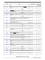
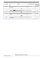
MPC8610CE
Rev. 0, 01/2010
Freescale Semiconductor
Chip Errata
MPC8610 Chip Errata
This document details all known silicon errata for the MPC8610 device.The following table provides a revision history
for this document.
Table 1. Document Revision History
Revision
Date
0
01/2010
Significant Changes
Initial public release
Revision Level to Part Marking Cross-Reference
The following table provides a cross-reference to match the revision code in the processor version register to the
revision level marked on the device.
Table 2. Revision Level to Part Marking Cross-Reference
Part
Revision
MPC8610 1.1
e600 Core Revision Device Marking
2.2
B
Processor Version Register
Value
0x8004_0202
System Version Register
Value
0x80A0_0011
Table 3 summarizes all known errata for blocks on the MPC8610 and lists the corresponding silicon revision level
to which it applies. A ‘Yes’ entry indicates the erratum applies to a particular revision level, while a ‘No’ entry means
it does not apply.
Note
Table 3. Summary of Silicon Errata and Applicable Revision
Errata
Name
Projected Solution
Silicon Rev.
1.1
DDR
DDR 1
Automatic data initialization and DLL resets to DRAM are not
performed correctly if CS2 and CS3 are interleaved
© Freescale Semiconductor , 2009. All Rights Reserved.
No plans to fix
Yes
Errata
Name
Projected Solution
Silicon Rev.
1.1
DDR 2
Memory contents may not be retained during HRESET sequence
No plans to fix
Yes
No plans to fix
Yes
No plans to fix
Yes
e600 1
Unexpected instruction fetch may occur when mtmsr/isync
No plans to fix
transitions MSR[IR] from 1 to 0 and isync instruction resides in
unmapped page
Yes
e600 2
core_mcp or core_sreset signal assertion during transition to
Nap may hang processor
No plans to fix
Yes
e600 3
Unpaired stwcx. may hang processor
No plans to fix
Yes
No plans to fix
Yes
2
2
2
Enabling I C could cause I C bus freeze when other I C devices No plans to fix
communicate
Yes
DMA
DMA 1
DMA_DACK bus timing violation when operating in external
DMA master mode
DUART
DUART 1
BREAK detection triggered multiple times for a single break
assertion
e600
GEN
GEN 1
CPU-only reset may result in a failure in the platform logic
I2C
I2C 1
JTAG
JTAG 1
Debug visibility unattainable without COP warm-up clock bit
set during HRESET assertion
No plans to fix
Yes
JTAG 2
Store-type operations during COP softstop debug mode may
hang processor; Machine check error limitations
No plans to fix
Yes
JTAG 3
Boundary scan test on SerDes transmitter pins needs special No plans to fix
requirement incompliant to IEEE 1149.1 specification
Yes
eLBC
eLBC1
Multi-bank DRAM and SDRAM will not work without any external No plans to fix
logic
Yes
eLBC 2
LTEATR and LTEAR may show incorrect values under certain No plans to fix
scenarios
Yes
eLBC 3
UPM does not have indication of completion of a Run Pattern No plans to fix
special operation
Yes
MCM
MCM 1
Unmapped tlbie EA causes local access window error
No plans to fix
Yes
PEX 2
Completion Timeout error disable corrupts CRS threshold error No plans to fix
data
Yes
PEX 3
No mechanism for recovery from hang after access to down
link
Yes
PEX
No plans to fix
MPC8610 Chip Errata, Rev. 0, 01/2010
2
Freescale Semiconductor
Errata
Name
Projected Solution
Silicon Rev.
1.1
PEX 4
Reads to PCI Express CCSRs or local config space temporarily No plans to fix
return all Fs
Yes
PCI
PCI 1
Assertion of STOP by a target device on the last beat of a PCI No plans to fix
memory write transaction can cause a hang
Yes
SPI
SPI 1
Selection of GPIO functionality on SPISEL signal causes MME No plans to fix
in SPI
Yes
PMON
PMON 1
Some local bus events are not counted correctly in the perform- No plans to fix
ance monitor
Yes
MPC8610 Chip Errata, Rev. 0, 01/2010
Freescale Semiconductor
3
DDR 1: Automatic data initialization and DLL resets to DRAM are not performed correctly
if CS2 and CS3 are interleaved
Description:
CS2 and CS3 can be interleaved together by setting
DDR_SDRAM_CFG[BA_INTLV_CTL] to 7'bx1xx0x0. In this mode, the DDR
controller may operate incorrectly for 2 different features.
First, the DDR controller will not initialize DRAM data properly if
DDR_SDRAM_CFG_2[D_INIT] is set. If D_INIT is set with CS2 and CS3
interleaved together, then the memory spaced defined by CS2 and CS3 will
not be initialized.
Second, the DDR controller may not issue DLL reset commands to CS2 and
CS3 when exiting self refresh.
Note that this feature is typically enabled when
DDR_SDRAM_CFG_2[DLL_RST_DIS] is cleared. If CS0 and CS1 are both
disabled via CSn_CONFIG[CS_n_EN] (and CS2 and CS3 are interleaved
together), then only CS3 will receive the DLL reset command when self refresh
is exited.
Note that neither of these issues will be present if all chip selects are enabled
and CS0-CS3 are interleaved together.
Impact:
There are 2 results that can be observed from this erratum. If the first scenario
listed above is present, then the memory space defined by CS2 and CS3 will
not be initialized properly when DDR_SDRAM_CFG_2[D_INIT] is set. If the
second scenario listed above is present, then the DLL reset command will
not be issued as expected to CS2. It is not expected that this will cause any
issues with DDR2 memories. DDR2 JEDEC specifications state that the
DRAM's DLL is automatically disabled when entering self refresh, and the
DLL is automatically reenabled when exiting self refresh. Although it would
be possible for some vendors to vary, the DLL reset should not be required
by the DRAMs when exiting self refresh. The DLL reset feature was originally
added to support DDR1 memories. It appears that DDR1 memories will
typically only require the DLL reset when the frequency is changed, but this
scenario should still be avoided if possible to prevent any potential issues.
Workaround:
There are several workarounds for this erratum. The preferred workaround
will be to disable interleaving between CS2 and CS3. CS0 and CS1 can still
be interleaved together. In addition, CS0 and CS3 could still be interleaved
together without any issues.
If it is still preferred to interleave CS2 and CS3 together, then one of two
workarounds can be used for initializing memory. First, software could be
used to initialize memory (i.e., via the DMA) instead of using
DDR_SDRAM_CFG_2[D_INIT]. In addition, the memory controller could be
enabled without CS2 and CS3 interleaved while
DDR_SDRAM_CFG_2[D_INIT] is set. After D_INIT is cleared by the hardware,
CS2 and CS3 could then be programmed to be interleaved together (via
DDR_SDRAM_CFG[BA_INTLV_CTL]). The memory space defined by the
CS2_BNDS register would then need to be updated to include the entire
memory space for CS2 and CS3. During this entire sequence, software would
need to guarantee that no other transactions are issued to memory.
MPC8610 Chip Errata, Rev. 0, 01/2010
4
Freescale Semiconductor
Other than disabling interleaving between CS2 and CS3, the only other way
to workaround the DLL reset issue is to ensure that either CS0 or CS1 is also
enabled (via CSn_CONFIG[CS_n_EN]).
Fix plan:
No plans to fix
MPC8610 Chip Errata, Rev. 0, 01/2010
Freescale Semiconductor
5
DDR 2: Memory contents may not be retained during HRESET sequence
Description:
It may be desirable for customers to have the DDR controller enter self refresh
mode and HRESET the part shortly after, while retaining contents of memory.
However, it is possible that CKE will not be driven active low during HRESET,
bringing the DRAM out of self refresh.
There are pin-sampled signals that may erroneously place the DDR into a
test mode if they are not set to a valid state when HRESET is asserted. The
DDR controller should drive the MCKE[0:3] pins active low throughout and
after HRESET. However, when this test mode is entered, the DDR drivers
will be inactive, and the MCKE[0:3] pins will be released to high impedance.
This test mode will be entered if a value of 0xf is presented on LA[28:31]
during HRESET, or if a value of 0x0 is presented on MSRCID[2] during
HRESET. The MCKE[0:3] pins will remain released to high impedance until
LA[28:31] and MSRCID[2] are set correctly for pin sampling.
There are POR configuration signals sampled during HRESET that do not
quickly achieve correct values using their internal pull-ups that may
erroneously place the chip into a test mode temporarily. The DDR controller
should drive the MCKE[0:3] pins active low throughout and after HRESET.
However, when the DDR controller enters a test mode, the DDR MCKE driver
will be released to high impedance or driven high, preventing the MCKE[0:3]
pins from being driven low immediately after HRESET.
This test mode will be entered if a value of 0xf is presented on LA[28:31]
during HRESET, a value of 0x0 is presented on TSEC2_TXD[4] and
TSEC2_TX_ER, or if a value of 0x0 is presented on D1_MSRCID[2] during
HRESET. The MCKE[0:3] pins will remain released to high impedance or
driven high until LA[28:31], TSEC2_TXD[4], TSEC2_TX_ER and
D1_MSRCID[2] are set correctly for pin sampling.
Impact:
The DRAMs may erroneously exit self refresh mode if MCKE is released to
high impedance and transitions above the minimum AC switching voltage
level.
Workaround:
Depending upon the board application, it may be possible to use active
components during HRESET to ensure that MCKE[0:3] will remain low
throughout HRESET.
Fix plan:
No plans to fix
MPC8610 Chip Errata, Rev. 0, 01/2010
6
Freescale Semiconductor
DMA 1: DMA_DACK bus timing violation when operating in external DMA master mode
Description:
The specification requires the external DMA master signal DMA_DACK to
be held for at least three system clocks. The DMA may violate this
requirement, depending on the internal latency of a transaction. The DMA
asserts DMA_DACK based on an internal 'write done' signal, which varies
depending on the write target and whether it is the last write of a transaction.
For MPX/platform to SYSCLK ratios of 9:1 or larger, in some cases, the 'write
done' signal asserts too quickly, causing the DMA_DACK to be held for too
short a time. MPX/platform to SYSYCLK ratios smaller than 9:1 are unaffected.
Impact:
DMA_DACK does not meet minimum hold specification of 3 SYSCLK cycles.
Workaround:
Option 1: Run MPX:SYSCLK ratio of 8:1 or smaller.
Option 2: Program the descriptors so each link descriptor can be handled in
one transaction. The last write of a descriptor uses a write-with-response
transaction, and therefore is delayed enough to meet the DMA_DACK spec
regardless of MPX:SYSCLK ratio.
Option 3:The following scenarios are the possible MPX:SYSCLK ratios greater
than 8:1 available on MPC8610 and their respective workarouds.
1. SYSCLK = 33 MHz, MPX = 333 (10:1), MPX:OCeaN = 1:1
Workaround: Use DMA byte count > 64 bytes, or do not rely on
DMA_DACK, or implement Option 2 above.
2. SYSCLK = 33 MHz, MPX = 333 (10:1), MPX:OCeaN = 2:1
This configuration is not affected by this erratum. The DMA controller
will function as expected.
3. SYSCLK = 33 MHz, MPX = 400 (12:1), MPX:OCeaN = 1:1
Workaround: Do not rely on DMA_DACK or implement Option 2 above.
4. SYSCLK = 33 MHz, MPX = 400 (12:1), MPX:OCeaN = 2:1
This configuration is not affected by this erratum. The DMA controller
will function as expected.
5. SYSCLK = 33 MHz, MPX = 533 (16:1), MPX:OCeaN = 1:1
This configuration is not supported on MPC8610. The MPX to OCeaN
ratio must be set to 2:1 through the cfg_net2_div configuration signal
for MPX frequencies above 400 MHz.
6. SYSCLK = 33 MHz, MPX = 533 (16:1), MPX:OCeaN = 2:1
This configuration is not affected by this erratum. The DMA controller
will function as expected.
Fix plan:
No plans to fix
MPC8610 Chip Errata, Rev. 0, 01/2010
Freescale Semiconductor
7
DUART 1: BREAK detection triggered multiple times for a single break assertion
Description:
A UART break signal is defined as a logic zero being present on the UART
data pin for a time longer than (START bit + Data bits + Parity bit + Stop bits).
The break signal persists until the data signal rises to a logic one.
A received break is detected by reading the ULSR and checking for BI=1.
This read to ULSR will clear the BI bit. Once the break is detected, the normal
handling of the break condition is to read the URBR to clear the ULSR[DR]
bit. The expected behavior is that the ULSR[BI] and ULSR[DR] bits will not
get set again for the duration of the break signal assertion. However, the
ULSR[BI] and ULSR[DR] bits will continue to get set each character period
after they are cleared. This will continue for the entire duration of the break
signal.
At the end of the break signal, a random character may be falsely detected
and received in the URBR, with the ULSR[DR] being set.
Impact:
The ULSR[BI] and ULSR[DR] bits will get set multiple times, approximately
once every character period, for a single break signal. A random character
may be mistakenly received at the end of the break.
Workaround:
The break is first detected when ULSR is read and ULSR[BI]=1. To prevent
the problem from occurring, perform the following sequence when a break is
detected:
1. Read URBR, which will return a value of zero, and will clear the
ULSR[DR] bit
2. Delay at least 1 character period
3. Read URBR again, which will return a value of zero, and will clear the
ULSR[DR] bit
ULSR[BI] will remain asserted for the duration of the break. The UART block
will not trigger any additional interrupts for the duration of the break.
This work around requires that the break signal be at least 2 character-lengths
in duration.
This work around applies to both polling and interrupt-driven implementations.
Fix plan:
No plans to fix
MPC8610 Chip Errata, Rev. 0, 01/2010
8
Freescale Semiconductor
e600 1: Unexpected instruction fetch may occur when mtmsr/isync transitions MSR[IR]
from 1→0 and isync instruction resides in unmapped page
Description:
If the mtmsr instruction is used to disable instruction translation, and the
subsequent isync instruction resides on a different page than the mtmsr
instruction, and the isync instruction’s page causes a page fault exception,
the e600 core will hang before taking the page fault exception. Once in the
hang state, the e600 core will not recover and hard reset must be asserted.
An alternate failing scenario can exist if the mtmsr and isync reside on the
same page but in different quadwords. If the mapping for that page exists in
the iTLB, but not the page table, and a tlbie snoop occurs between the mtmsr
and isync that invalidates the iTLB entry, then the processor will hang before
taking the page fault exception.
If the isync instruction address is guaranteed to have a valid page table
mapping resident in the memory hierarchy, then neither scenario can occur.
Impact:
Any systems that disable instruction translation using mtmsr, and for which
the required isync may reside in a different page whose page table entry is
not available in the memory hierarchy may hang.
Any systems mapping the mtmsr/isync code with the IBATs will not fail due
to this issue. Any systems not demand-paging their supervisor-level code will
not fail due to this issue.
Workaround:
Any of the following work-arounds will avoid the e600 core from hanging:
• mtmsr/isync instruction pairs should reside within the same quadword.
• disable instruction translation by initializing SRR0/SRR1 and executing
rfi.
• map code which disables instruction address translation with the IBATs.
Fix plan:
No plans to fix
MPC8610 Chip Errata, Rev. 0, 01/2010
Freescale Semiconductor
9
e600 2: core_mcp or core_sreset signal assertion during transition to Nap may hang
processor
Description:
On the MPC8610, all internal interrupt signals to the processor core, excluding
core_smi, are prioritized and delivered by the programmable interrupt controller
(PIC). The core_smi signal is delivered to the processor via the global utilities
block from the external SMI signal. Please refer to the PIC chapter in the
device reference manual for more information on these internal signals.
If the machine check signal (core_mcp) or soft reset signal (core_sreset) are
asserted in a window after MSR[POW] has been set but before the processor
has asserted the quiesce request signal (qreq), then the processor may
encounter a hang condition.
The nap entry sequence in the e600 Core User’s Manual is as follows:
loop: sync
mtmsr POW
isync
b loop
Legacy software entering nap using this entry sequence are not affected:
sync
mtmsr POW
isync
loop: b loop
The fail occurs when an outstanding out-of-order instruction fetch occurring
before the mtmsr, but not having received data and the results of which are
no longer needed for execution, extends the window between the setting of
POW and the assertion of qreq by the processor. If the Branch Target
Instruction cache (BTIC) is enabled, and the Nap entry code is in the BTIC
due to a previous execution of this code, then the instructions from the
sequence can be loaded into the completion buffer the cycle after execution
has halted. If the core_mcp or core_sreset signals are asserted at this point,
they will void the entry into Nap as architected. However, both events require
the completion buffer to be empty for their exceptions to be processed.
Completion is halted, though, so no exceptions are processed and the hang
occurs. The core_smi and int signal assertions do not require the completion
buffer to be empty and therefore do not cause a hang.
Impact:
Systems where core_mcp or core_sreset can be asserted during entry into
Nap mode are at risk. On the MPC8610 processor, critical interrupts, including
Message-Shared, Message, and External interrupt sources, are mapped to
the e600 core_mcp input. Therefore, risk of failure is greater than for devices
with external interrupt signals to the processor cores.
Workaround:
Systems can implement any one of the following changes to work around
this issue:
1. Use the legacy code entry sequence to enter Nap.
2. Disable the BTIC before entering Nap.
MPC8610 Chip Errata, Rev. 0, 01/2010
10
Freescale Semiconductor
3. Invalidate the Nap entry code using an icbi instruction after taking the
exception (a decrementer exception for example) that awakens the
processor from Nap state.
Fix plan:
No plans to fix
MPC8610 Chip Errata, Rev. 0, 01/2010
Freescale Semiconductor
11
e600 3: Unpaired stwcx. may hang processor
Description:
In general, lwarx and stwcx. instructions should be paired, with the same
effective address used for both.The only exception is that an unpaired stwcx.
instruction to any (scratch) effective address can be used to clear any
reservation held by the processor.
When a stwcx. is unpaired, the e600 core may encounter an unexpected
hang condition if each of the following is true:
1. Initial condition
RESERVE bit = 1 (due to previously executed lwarx)
Reservation = address A
Instruction executed = stwcx. to address B, resident in
dL1 in Modified or Exclusive state
dL1 modified entry = address C
2. An external snoop to address A of a type shown in the following table
occurs while the stwcx. is being processed by the Load/Store Unit.
Table 4. Snooped Store Types that Cancel a Reservation
Command
TT
Write-with-flush
0x02
Write-with-kill
0x06
Kill block
0x0C
Read-with-intent-to-modify
0x0E
Read claim
0x0F
Read-with-intent-to-modify-atomic (stwcx.)
0x1E
3. An external snoop to address C follows the snoop to address A while
the stwcx. is being processed by the Load/Store Unit.
Normally, the snoop to address A would clear the RESERVE bit, and the
snoop to address C would initiate a snoop push of the modified line from the
dL1. The stwcx. may succeed or fail depending on when the snoop to A
cleared the RESERVE bit, but the completion of the stwcx. should be reported
regardless.
A one cycle window exists wherein the above sequence will cause the
Load/Store Unit to not report the completion of the stwcx. to the Completion
Unit. As a result, the processor will hang. The hang can only be cleared by
asserting hard reset.
Impact:
The processor will hang if the Load/Store Unit does not report the completion
of the stwcx. to the completion unit. Paired lwarx/stwcx. instructions are not
affected by this erratum. Most operating systems include an unpaired stwcx.
at the end of exception handler code and context switch code to clear the
RESERVE bit before returning to normal execution. Note that stwcx. is a
user level instruction.
MPC8610 Chip Errata, Rev. 0, 01/2010
12
Freescale Semiconductor
Non-SMP environments are less susceptible to this erratum due to the
requirement of an external snoop to address A which holds the reservation
from a previous lwarx instruction. Most operating systems do not allow a
snoop to be initiated by an external peripheral to an address that the core
wants to reserve in a non-SMP environment. If the non-SMP environment's
operating system does not allow such snoops, then the environment will not
be affected by this erratum.
Workaround:
Any individual one of the following steps can be taken to work around this
issue:
• Place a lwarx instruction to the same scratch address as the stwcx.
immediately before the stwcx., or
• Place a dcbf instruction to the same scratch address as the stwcx.
immediately before the stwcx., or
• Do not permit an external snoop to the address of the reservation
address.
Interrupts must be disabled (MSR[EE] = 0) during the instruction sequences
for the first two options. In most operating systems, interrupts are already
disabled when an unpaired stwcx. is executed.
Fix plan:
No plans to fix
MPC8610 Chip Errata, Rev. 0, 01/2010
Freescale Semiconductor
13
GEN 1: CPU-only reset may result in a failure in the platform logic
Description:
The device provides the ability to assert the core_sreset signal to the
processor. Once done, the possibility exists that the platform logic may fail.
Impact:
If core_sreset is asserted by setting PIR[P0], the possibility exists that the
platform logic may fail.
Workaround:
The core must be reset via a full hard reset of the device.
Fix plan:
No plans to fix
MPC8610 Chip Errata, Rev. 0, 01/2010
14
Freescale Semiconductor
I2C 1: Enabling I2C could cause I2C bus freeze when other I2C devices communicate
Description:
2
When the I C controller is enabled by software, if the signal SCL is high, the
2
signal SDA is low, and the I C address matches the data pattern on the SDA
bus right after enabling, an ACK is issued on the bus. The ACK is issued
2
because the I C controller detects a START condition due to the nature of
the SCL and SDA signals at the point of enablement. When this occurs, it
2
may cause the I C bus to freeze. However, it happens very rarely due to the
need for two conditions to occur at the same time.
2
2
2
Impact:
Enabling the I C controller may cause the I C bus to freeze while other I C
devices communicate on the bus.
Workaround:
Use one of the following workarounds:
• Enable the I2C controller before starting any I2C communications on the
bus. This is the preferred solution.
• If the I2C controller is configured as a slave, implement the following
steps:
a. Software enables the device by setting I2CnCR[MEN] = 1 and
starts a timer.
b. Delay for 4 I2C bus clocks.
c. Check Bus Busy bit (I2CnSR[MBB])
if MBB == 0
jump to Step f; (Good condition. Go
to Normal operation)
else
Disable Device (I2CnCR[MEN] = 0)
d. Reconfigure all I2C registers if necessary.
e. Go back to Step a.
f. Normal operation.
Fix plan:
No plans to fix
MPC8610 Chip Errata, Rev. 0, 01/2010
Freescale Semiconductor
15
JTAG 1: Debug visibility unattainable without COP warm-up clock bit set during HRESET
assertion
Description:
There is no debug visibility unless the warm-up clock bit, only accessible
through the COP, is set during HRESET assertion.
Impact:
An HRESET assertion on the board is required to gain debug visibility because
the warm-up clock bit must be set during HRESET assertion. Debug of the
device is not obtainable until the warm-up bit is set during HRESET assertion.
All systems in development and in production will be affected including the
following systems:
•
•
•
•
Workaround:
Systems with the MPC8610 on a daughter card
Systems in the field
Systems in test before final production
Systems in hardware and software debug labs
Set the warm-up clock bit via the COP tool during HRESET assertion. This
temporary solution will allow for debug visibility on lab and testing systems
that can afford to be reset while debugging. However, for systems in the field
this may not be an option because a reset will cause all error data to be lost.
For systems where the MPC8610 is on a daughter card, the above workaround
will not solve the issue. A reset of the daughter card will set the warm-up
clock bit, but the card itself will not be reliable for several reasons (i.e. it will
not be synchronized with the motherboard and may not be able to be reset
without a reset from the motherboard) There is not workaround for this type
of system.
Fix plan:
No plans to fix
MPC8610 Chip Errata, Rev. 0, 01/2010
16
Freescale Semiconductor
JTAG 2: Store-type operations during COP softstop debug mode may hang processor;
Machine check error limitations
Description:
During softstop debug mode, the processor may incorrectly disable internal
clocks before a store type operation has accessed the Platform/MPX bus.
Softstop debug mode is accessible via the common on-chip processor (COP)
and is used by emulator tools for debugging. The store type operations
affected are:
CI store
WT store
eieio
tlbsync
tlbie
dcbf
dcbf w/ data
castout
dcbi
icbi
ecowx
The store type operation would be retained in the bus store queue while the
clocks were frozen. The retained store may cause the processor to violate
the bus protocol either before entering or after resuming from softstop. The
resulting protocol violation may hang the system, and require a hard reset to
recover.
Possible protocol violations include but are not limited to:
1. A multi-cycle assertion of TS as softstop is entered.
2. A TS assertion after resuming from softstop that may not meet proper
setup time.
3. A TS assertion after resuming from softstop that is not preceded by a
qualified BG assertion.
4. A missed AACK assertion.
Softstop debug mode via the COP is affected. Using the IABR/DABR and
taking a trace or performance monitor interrupt during functional mode works
as expected. The QREQ/QACK nap/sleep protocol also works as expected.
The COP softstop operations affected are those triggered by:
1.
2.
3.
4.
A direct COP softstop request.
An IABR or DABR match event.
An MSR[SE] or MSE[BE] event.
A performance monitor event.
The issue also affects functional operation mode. Normally, when a machine
check exception occurs, any store type operations in the pipeline of the
processor are required to complete to memory before the machine check
exception is taken. Due to the erratum, the machine check exception may be
taken while a solitary store type operation is present in the bus store queue.
The only known impact of this behavior occurs if the solitary store type
operation encounters a parity error or TEA error on the Platform/MPX bus,
then the processor would checkstop due to taking a machine check exception
while in the machine check exception handler.
Impact:
Emulators that utilize the COP softstop feature may not work as intended
since the processor’s violation of the system bus protocol may cause
unexpected behavior on the part of the system controller.
Extra delay is added between entry into softstop and the disabling of clocks
on the MPC8610. Due to this characteristic the failure is very unlikely. This
erratum has not been observed on the MPC8610, but the possibility still exists.
MPC8610 Chip Errata, Rev. 0, 01/2010
Freescale Semiconductor
17
Workaround:
Customers may be able to find Core:MPX multiplier ratios that do not result
in the processor hanging the system when this erratum is encountered; the
address and address transfer attributes may have a modified output valid
timing but may be sufficient to meet the receiving device’s input setup times.
If this erratum is encountered, debugging software at another Core:MPX ratio
is possible. The store type operations will not complete until resuming from
softstop state or single-stepping beyond the store type operation. Enabling
address bus parking with the processor will reduce the chance of incurring
this erratum.
Fix plan:
No plans to fix
MPC8610 Chip Errata, Rev. 0, 01/2010
18
Freescale Semiconductor
JTAG 3: Boundary scan test on SerDes transmitter pins needs special requirement
incompliant to IEEE 1149.1 specification
Description:
The IEEE 1149.1 EXTEST or CLAMP specification requires to drive all
output/bidirectional pins to a logical 1 at the same time. However, if this
requirement is followed when executing the 1149.1 EXTEST or CLAMP
command to drive SerDes transmitter pins, incorrect data will be present on
SerDes pins during the boundary scan test.
Impact:
A user will have to scan in all zeroes to the boundary cells associated with
non-SerDes pins when testing the SerDes pins. There is no requirement in
regards to testing all other pins.
Workaround:
When executing the 1149.1 EXTEST or CLAMP command to drive SerDes
transmitter pins, the user must scan in logic 0 to the boundary cells associated
with non-SerDes pins, or configure all non-SerDes pins as inputs.
Fix plan:
No plans to fix
MPC8610 Chip Errata, Rev. 0, 01/2010
Freescale Semiconductor
19
eLBC1: Multi-bank DRAM and SDRAM will not work without any external logic
Description:
When the UPM is connected to multi-bank DRAM and SDRAM, the memories
require that the bank address should be driven during both RAS and CAS
cycles. However, due to the internal implementation, that does not happen.
Impact:
Multi-bank memories (DRAM/SDRAM) will not work as expected with the
UPM.
Workaround:
An external intelligent logic can be used on the board as a workaround.
Fix plan:
No plans to fix
MPC8610 Chip Errata, Rev. 0, 01/2010
20
Freescale Semiconductor
eLBC 2: LTEATR and LTEAR may show incorrect values under certain scenarios
Description:
The eLBC IP acks any transaction request when FCM special operation is in
progress. In such a scenario when any one of the errors/events occur (such
as Bus Monitor Timeout, Write Protect, Parity error, Atomic error, FCM
command completion, or UPM command completion except for the CS error),
the registers LTEAR and LTEATR capture the address and attributes of the
most recently req-acked transaction instead of the FCM special operation
that caused error. Hence indeterministic value may show up in those registers.
Impact:
LTEAR and LTEATR cannot be used for debugging in this scenario.
Workaround:
None
Fix plan:
No plans to fix
MPC8610 Chip Errata, Rev. 0, 01/2010
Freescale Semiconductor
21
eLBC 3: UPM does not have indication of completion of a Run Pattern special operation
Description:
A UPM or FCM special operation is initiated by writing to MxMR[OP] or
FCM[OP] and then triggering the special operation either through the LSOR
register or by performing a dummy access to the bank.
The UPM and FCM are expected to have different indications of when the
special operation is completed.The FCM will see the LTESR[CC] bit set when
such a special operation is completed. The UPM will see MxMR[MAD]
increment when a write to or read from UPM array special operation
completes. However, the UPM does not have any status indication of
completion of the run pattern special operation.
The following two scenarios could be affected by this erratum:
1. A UPM Run Pattern special operation is initiated and a second UPM
command is issued before the Run Pattern is completed.
If the above scenario occurs the programmed mode registers could be
altered according to the second operation and cause the current/first
operation to encounter errors due to mode changes in the middle of the
operation. Note that if the second command issued is a Run Pattern
operation and it does not change the mode registers, the first operation
should not encounter errors.
2. A write to LSOR initiates a UPM Run Pattern special operation and then
LSOR is written too again, to initiate a second special operation that
requires the mode registers to change while the first Run Pattern
operation is in progress.
If the second special operation issued does not change the programming
mode of the first Run Pattern operation because the operation is either
exactly the same as the first or it requires programming of an
independent set of registers then the Run Pattern operation should not
encounter errors.
The behavior of the eLBC is unpredictable if the Run Pattern special operation
mode is altered between initiation of the operation and the relevant memory
controller completing the operation.
Impact:
Because of this erratum, when a UPM run pattern special operation is to be
followed by any other UPM command for which the mode registers need to
change, the Run Pattern operation may not be handled properly. Software
does not have any means to confirm when the current run pattern special
operation has completed so that register programming for the next operation
can be done safely.
Workaround:
None
Fix plan:
No plans to fix
MPC8610 Chip Errata, Rev. 0, 01/2010
22
Freescale Semiconductor
MCM 1: Unmapped tlbie EA causes local access window error
Description:
A tlbie transaction uses an effective address rather than a real address, and
should not participate in system address mapping in the MCM because tlbie
is an address only transaction. However, if the effective address in a tlbie
transaction does not match any local access window (LAW) in the MCM, it
will trigger a local access error by setting EDR[LAE] = 1 and an interrupt when
EER[LAEE] = 1.
Impact:
A tlbie transaction may cause a local access error.
Workaround:
Option 1: Enable local access error interrupts by EER[LAEE] = 1. When the
MCM reports detected errors as interrupts, clear EDR[LAE] bit by writing a
b'1 to EDR[LAE] if the following conditions are all true:
1. EDR[LAE] is set.
2. EATR[SRC_ID] = 10000 (core instruction)
3. EATR[TTYPE] is 1010.
Option 2: Set HID1[ABE] = 0. This will prevent the broadcasting of tlbie, as
well as other cache operations (dcbf, dcbst, dcbi, icbi) and tlbsync.
Fix plan:
No plans to fix
MPC8610 Chip Errata, Rev. 0, 01/2010
Freescale Semiconductor
23
PEX 2: Completion Timeout error disable corrupts CRS threshold error data
Description:
Several attributes of enabled error conditions are written to the PEX Error
Capture Status register (offset 0xE20) when an error condition is detected.
If PEX_ERR_DISR[PCTD]=1 (disable detection of Completion Timeout
threshold errors), then the global source ID attribute
(PEX_ERR_CAP_R2[19:24]) for CRS Threshold errors will be incorrect.
Impact:
An incorrect global source ID is captured in PEX Error Capture Status register
for CRS Threshold errors if Completion Timeout errors are disabled.
Workaround:
Enable Completion Timeout and CRS threshold error detection by keeping
the default setting of PEX_ERR_DISR[PCTD]=0 and
PEX_ERR_DISR[CRSTD] = 0.
Fix plan:
No plans to fix
MPC8610 Chip Errata, Rev. 0, 01/2010
24
Freescale Semiconductor
PEX 3: No mechanism for recovery from hang after access to down link
Description:
When its link goes down, the PCI Express controller clears all outstanding
transactions with an error indicator and sends a link down exception to the
interrupt controller if PEX_PME_MES_DISR[LDDD] = 0. If, however, any
transactions are sent to the controller after the link down event, they will be
accepted by the controller and wait for the link to come back up before starting
any timeout counters (e.g. completion timeout). There is no mechanism to
cancel the new transactions short of a device HRESET.
Impact:
New transactions sent to a PCI Express link which is down will not complete
or invoke a recoverable time out until the link recovers. The outstanding
transactions may cause a core or other master (e.g. DMA) hang or a core
watchdog timeout.
Workaround:
The problem can be mitigated by ensuring that link down exceptions are
enabled (PEX_PME_MES_DISR[LDDD] = 0), and cause access to the PCI
Express interface to be disabled for the duration of the link down. Note that
PCI Express controller access can be via normal reads and writes (LAW/ATMU
target) or by reads or writes to CONFIG_DATA in the PCI Express controller
memory-mapped register space. Both types of access must be prevented.
This does not completely eliminate the problem, because there could be
accesses to the PCI Express interface between the time the link goes down
and the time the interrupt handler disables access to the interface. In this
instance device HRESET is required.
Fix plan:
No plans to fix
MPC8610 Chip Errata, Rev. 0, 01/2010
Freescale Semiconductor
25
PEX 4: Reads to PCI Express CCSRs or local config space temporarily return all Fs
Description:
When its link goes down the PCI Express controller clears all outstanding
transactions and, if PEX_PME_MES_DISR[LDDD]=0 and
PEX_PME_MES_IER[LDDIE]=1, sends a link down exception to the interrupt
controller. Read transactions are cleared with an error indicator (transaction
error to source for memory reads, return data all Fs for config reads). Write
transactions are silently dropped.
The canceling of config read or write transactions should not apply to accesses
to configuration, control and status registers in memory-mapped space or
local PCI Express config space. Writes to memory-mapped or local PCI
Express config registers are handled normally. However, due to this erratum,
reads return all Fs for the duration of the link down cleanup.
If the controller is configured as an endpoint and receives a hot reset request,
it also brings the link down and follows the same cleanup procedures as in
an externally detected link down. Note that reads to PCI Express
memory-mapped registers or config registers will return all Fs for the duration
of the hot reset event, as well.
Impact:
Reads to configuration, control and status registers in the memory-mapped
or config space of PCI Express return all Fs during link down cleanup or hot
reset event.
During this time, writes are handled normally, though the results of the write
are not verifiable.
The duration of the link down cleanup varies depending on the number and
type of pending transactions. Cleanup for pending outbound transactions
takes just a few cycles, regardless of the source. Pending inbound transactions
wait for all responses from targets (data response for reads, or successful
arbitration to the target queue for writes) before completing cleanup.
Once all pending transactions have been cleared, new CCSR accesses and
local config return to normal operation.
Note that because of PEX 3, any new accesses to PCI Express, including
config reads to off-chip registers, will wait until the link resumes normal
operation to complete. The config access state machine is serialized, so a
config read to an off-chip register will prevent access to local CCSRs or local
config operations while the link remains down.
Workaround:
If the configuration, control or status register cannot return all Fs as a legal
value, but does, keep polling the register value until it is not all Fs. Note that
PEX_PME_MES_DR, the detect register containing the link down detect bit,
cannot return all Fs in normal operation.
If the configuration, control or status register can return all Fs as a legal value,
and does, read another register which is known not to contain all Fs (e.g.
PEX_IP_BLK_REV1) to confirm that the link is not in hot reset or link down
cleanup, then reread the original register.
Fix plan:
No plans to fix
MPC8610 Chip Errata, Rev. 0, 01/2010
26
Freescale Semiconductor
PCI 1: Assertion of STOP by a target device on the last beat of a PCI memory write
transaction can cause a hang
Description:
As a master, the PCI IP block can combine a memory write to the last PCI
double word (4 bytes) of a cacheline with a 4 byte memory write to the first
PCI double word of the subsequent cacheline.
This only occurs if the second memory write arrives to the PCI IP block before
the deassertion of FRAME for the first write transaction. If the writes are
combined, the PCI IP block masters a single memory-write transaction on
the PCI bus. If for this transaction, the PCI target asserts STOP during the
last data beat of the transaction (FRAME is deasserted, but TRDY and
IRDYare asserted), the transaction completes correctly. A subsequent write
transaction other than an 8-byte write transaction causes a hang on the bus.
Two different hang conditions can occur:
• If the target disconnects with data on the first beat of this last write
transaction, the PCI IP block deasserts IRDY on the same cycle as it
deasserts FRAME (PCI protocol violation), and no more transactions
will be mastered by the PCI IP block.
• If the target does not disconnect with data on the first beat of this last
write transaction, IRDY will be deasserted after the first beat is
transferred and will not be asserted anymore after that, causing a hang.
Impact:
This affects 32-bit PCI target devices that blindly assert STOP on
memory-write transactions, without detecting that the data beat being
transferred is the last data beat of the transaction. It can cause a hang.
If the PCI transaction is a one data beat transaction and the target asserts
STOP during the transfer of that beat, there is no impact.
Workaround:
A PCI target device could avoid asserting STOP# during the last beat of a
PCI memory write transaction that is greater than one data beat and crosses
a cacheline boundary. It could assert STOP# during the last data beat of the
cacheline or not assert STOP# at all. A software workaround for this problem
is to set the PCI Latency Timer Register (offset 0x0D) to zero. A value of zero
is the reset value for this register, so if this register is kept unmodified after
reset, it will prevent the PCI IP block from ever combining writes.
A debug bit, bit 10 of the PCI Bus Function Register (address 0x44) has been
identified as another workaround. This bit, MDS (Master disable streaming),
when set, will disable the combining of crossing cacheline boundary requests
into one burst transaction,. Therefore, it can prevent the errata scenario from
occurring. When this bit 10 is set, customer can program the PCI Latency
Timer to achieve full cacheline burst even with one request in the PCI pipe.
Fix plan:
No plans to fix
MPC8610 Chip Errata, Rev. 0, 01/2010
Freescale Semiconductor
27
SPI 1: Selection of GPIO functionality on SPISEL signal causes MME in SPI
Description:
If SPI is being used in master mode and the SPISEL signal is programmed
to operate with GPIO functionality (GPIOCR[UART0]=11 for SPI
andGPIOCR[I2C2_SDA]=1 for GPIO), a multiple master error (MME) can
occur if the pin is driven low due to the fact that the pin retains the SPISEL
functionality in addition to the programmed GPIO functionality.
Impact:
While using SPI in master mode, GPIO2[12] cannot be used to select slave
devices.
Workaround:
GPIOCR[I2C2_SDA] should be set to 1b'0 when GPIOCR[UART0] is set to
2b'11 and SPI is used in master mode (SPMODE[M/S]=1). When in master
mode, a separate GPIO should be used to act as a slave select. As described
in the reference manual, if the SPI is used in single-master mode, the master's
SPISEL input should be forced inactive by an external pull up.
Fix plan:
No plans to fix
MPC8610 Chip Errata, Rev. 0, 01/2010
28
Freescale Semiconductor
PMON 1: Some local bus events are not counted correctly in the performance monitor
Description:
The "Number of accesses hitting banks (chip-selects) 1-8" events for the
eLBC are not counted correctly.
Impact:
These local bus events can not be used in the performance monitor.
Workaround:
None
Fix plan:
No plans to fix
MPC8610 Chip Errata, Rev. 0, 01/2010
Freescale Semiconductor
29
How to Reach Us:
Home Page:
www.freescale.com
Web Support:
http://www.freescale.com/support
USA/Europe or Locations Not Listed:
Freescale Semiconductor, Inc.
Technical Information Center, EL516
2100 East Elliot Road
Tempe, Arizona 85284
1-800-521-6274 or
+1-480-768-2130
www.freescale.com/support
Europe, Middle East, and Africa:
Freescale Halbleiter Deutschland GmbH
Technical Information Center
Schatzbogen 7
81829 Muenchen, Germany
+44 1296 380 456 (English)
+46 8 52200080 (English)
+49 89 92103 559 (German)
+33 1 69 35 48 48 (French)
www.freescale.com/support
Information in this document is provided solely to enable system and software
implementers to use Freescale Semiconductor products. There are no express or
implied copyright licenses granted hereunder to design or fabricate any integrated
circuits or integrated circuits based on the information in this document.
Freescale Semiconductor reserves the right to make changes without further notice to
any products herein. Freescale Semiconductor makes no warranty, representation or
guarantee regarding the suitability of its products for any particular purpose, nor does
Freescale Semiconductor assume any liability arising out of the application or use of
any product or circuit, and specifically disclaims any and all liability, including without
limitation consequential or incidental damages. “Typical” parameters which may be
provided in Freescale Semiconductor data sheets and/or specifications can and do
vary in different applications and actual performance may vary over time. All operating
parameters, including “Typicals” must be validated for each customer application by
customer’s technical experts. Freescale Semiconductor does not convey any license
Japan:
Freescale Semiconductor Japan Ltd.
Headquarters
ARCO Tower 15F
1-8-1, Shimo-Meguro, Meguro-ku
Tokyo 153-0064
Japan
0120 191014 or
+81 3 5437 9125
[email protected]
under its patent rights nor the rights of others. Freescale Semiconductor products are
Asia/Pacific:
Freescale Semiconductor China Ltd.
Exchange Building 23F
No. 118 Jianguo Road
Chaoyang District
Beijing 100022
China
+86 10 5879 8000
[email protected]
claims, costs, damages, and expenses, and reasonable attorney fees arising out of,
For Literature Requests Only:
Freescale Semiconductor
Literature Distribution Center
P.O. Box 5405
Denver, Colorado 80217
1-800 441-2447 or
+1-303-675-2140
Fax: +1-303-675-2150
LDCForFreescaleSemiconductor
@hibbertgroup.com
Document Number: MPC8610CE
Rev. 0
01/2010
not designed, intended, or authorized for use as components in systems intended for
surgical implant into the body, or other applications intended to support or sustain life,
or for any other application in which the failure of the Freescale Semiconductor product
could create a situation where personal injury or death may occur. Should Buyer
purchase or use Freescale Semiconductor products for any such unintended or
unauthorized application, Buyer shall indemnify and hold Freescale Semiconductor
and its officers, employees, subsidiaries, affiliates, and distributors harmless against all
directly or indirectly, any claim of personal injury or death associated with such
unintended or unauthorized use, even if such claim alleges that Freescale
Semiconductor was negligent regarding the design or manufacture of the part.
Freescale and the Freescale logo are trademarks or registered trademarks
of Freescale Semiconductor, Inc. in the U.S. and other countries. All other
product or service names are the property of their respective owners. The
Power Architecture and Power.org word marks and the Power and
Power.org logos and related marks are trademarks and service marks
licensed by Power.org. IEEE 1149.1 is a registered trademark of the Institute
of Electrical and Electronics Engineers, Inc. (IEEE). This product is not
endorsed or approved by the IEEE.
© Freescale Semiconductor, Inc., 2010.