1
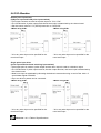
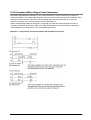
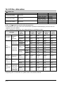
Safety Precautions
Observe the following notices to ensure personal safety or to prevent accidents.
To ensure that you use this product correctly, read this User’s Manual thoroughly before use.
Make sure that you fully understand the product and information on safety.
This manual uses two safety flags to indicate different levels of danger.
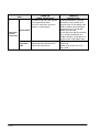
WARNING
If critical situations that could lead to user’s death or serious injury is assumed by
mishandling of the product.
-Always take precautions to ensure the overall safety of your system, so that the whole
system remains safe in the event of failure of this product or other external factor.
-Do not use this product in areas with inflammable gas. It could lead to an explosion.
-Exposing this product to excessive heat or open flames could cause damage to the lithium
battery or other electronic parts.
-Battery may explode if mistreated. Do not recharge, disassemble or dispose of fire.
CAUTION
If critical situations that could lead to user’s injury or only property damage is
assumed by mishandling of the product.
-To prevent excessive exothermic heat or smoke generation, use this product at the values
less than the maximum of the characteristics and performance that are assured in these
specifications.
-Do not dismantle or remodel the product. It could cause excessive exothermic heat or smoke
generation.
-Do not touch the terminal while turning on electricity. It could lead to an electric shock.
-Use the external devices to function the emergency stop and interlock circuit.
-Connect the wires or connectors securely.
The loose connection could cause excessive exothermic heat or smoke generation.
-Do not allow foreign matters such as liquid, flammable materials, metals to go into the inside
of the product. It could cause excessive exothermic heat or smoke generation.
-Do not undertake construction (such as connection and disconnection) while the power
supply is on. It could lead to an electric shock.
Copyright / Trademarks
-This manual and its contents are copyrighted.
-You may not copy this manual, in whole or part, without written consent of Panasonic
Industrial Devices SUNX Co., Ltd.
-Windows is a registered trademark of Microsoft Corporation in the United States and other
countries.
-All other company names and product names are trademarks or registered trademarks of
their respective owners.
PLC_BAT
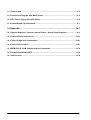
Table of Contents
Before You Start
Differences in Functions Between Versions of Controller
Programming Tool Restrictions
When Changing Ladder Program from 12k Type to 32k Type
Compatibility with FP0
Manuals to be Used
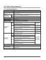
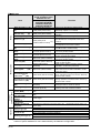
1 Functions and Restrictions of the Unit .................................................. 1-1
1.1 Features and Functions of the Unit ............................................................................... 1-2
1.2 Unit Types ........................................................................................................................ 1-6
1.3 Restrictions on Unit Combinations ............................................................................. 1-12
1.4 Programming Tools ....................................................................................................... 1-14
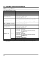
2 Specifications and Functions of the Unit .............................................. 2-1
2.1 Parts and Functions ........................................................................................................ 2-2
2.2 Input and Output Specifications .................................................................................... 2-6
2.3 Terminal Layout Diagram ............................................................................................. 2-11
2.4 Analog Potentiometer ................................................................................................... 2-13
2.5 Thermister Input (Only for TM type) ............................................................................ 2-14
2.6 Clock/Calendar Function .............................................................................................. 2-17
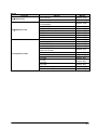
3 Expansion................................................................................................. 3-1
3.1 Type of Expansion Unit ................................................................................................... 3-2
3.2 Expansion Method of FP0/FP0R Expansion Unit ......................................................... 3-3
3.3 Expansion Method of FPΣ Expansion Unit ................................................................... 3-4
3.4 Specifications of FPΣ Expansion Unit ........................................................................... 3-5
4 I/O Allocation ............................................................................................ 4-1
4.1 I/O Allocation .................................................................................................................... 4-2
4.2 Allocation of FPΣ Control Unit ....................................................................................... 4-3
i
4.3 Allocation of FPΣ Expansion Unit .................................................................................. 4-4
4.4 Allocation of FP0/FP0R Expansion Unit ........................................................................ 4-5
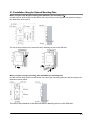
5 Installation and Wiring............................................................................. 5-1
5.1 Installation ........................................................................................................................ 5-2
5.2 Wiring of Power Supply .................................................................................................. 5-8
5.3 Wiring of Input and Output ........................................................................................... 5-11
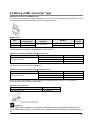
5.4 Wiring of MIL Connector Type...................................................................................... 5-15
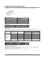
5.5 Wiring of Terminal Block Type ..................................................................................... 5-17
5.6 Safety Measures ............................................................................................................ 5-19
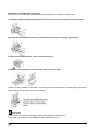
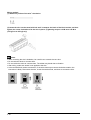
5.7 Handling of Backup Battery.......................................................................................... 5-21
6 High-speed counter, Pulse Output and PWM Output functions .......... 6-1
6.1 Overview of Each Functions........................................................................................... 6-2
6.3 High-speed Counter Function ...................................................................................... 6-10
6.4 Pulse Output Function .................................................................................................. 6-18
6.5 PWM Output Function ................................................................................................... 6-58
7 Communication Cassette ........................................................................ 7-1
7.1 Functions and Types ....................................................................................................... 7-2
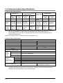
7.2 Communication Specifications .................................................................................... 7-10
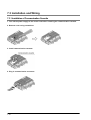
7.3 Installation and Wiring .................................................................................................. 7-14
7.4 Communication Function 1: Computer Link ............................................................... 7-18
7.5 Communication Function: General-purpose Serial Communication ....................... 7-35
7.6 Communication Function 3: PC(PLC) link .................................................................. 7-50
7.7 Communication Function 4: MODBUS RTU Communication ................................... 7-71
8 Security Functions ................................................................................... 8-1
8.1 Type of Security Functions............................................................................................. 8-2
ii
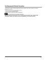
8.2 Password Protect Function ............................................................................................ 8-3
8.3 Upload Protection FPΣ 32k Type Only ........................................................................ 8-10
8.4 Setting Function for FP Memory Loader ..................................................................... 8-11
8.5 Table of Security Settings/Cancel................................................................................ 8-15
9 Other Functions ....................................................................................... 9-1
9.1 P13 (ICWT) Instruction .................................................................................................... 9-2
9.2 Sampling Trace Function 32k Type Only .................................................................... 9-3
10 Self-Diagnostic and Troubleshooting ................................................ 10-1
10.1 Self-Diagnostic function ............................................................................................. 10-2
10.2 Troubleshooting .......................................................................................................... 10-3
11 Precautions During Programming...................................................... 11-1
11.1 Use of Duplicated Output ........................................................................................... 11-2
11.2 Handling BCD Data ...................................................................................................... 11-4
11.3 Handling Index Registers ........................................................................................... 11-5
11.4 Operation Errors .......................................................................................................... 11-7
11.5 Instruction of Leading Edge Detection Method........................................................ 11-9
11.6 Precautions for Programming .................................................................................. 11-13
11.7 Rewrite Function During RUN .................................................................................. 11-14
11.8 Processing During Forced Input and Output ......................................................... 11-19
12 Specifications ...................................................................................... 12-1
12.1 Table of Specifications ............................................................................................... 12-2
12.2 I/O No. Allocation ....................................................................................................... 12-12
12.3 Relays, Memory Areas and Constants .................................................................... 12-14
13 Dimensions .......................................................................................... 13-1
iii
13.1 Dimensions .................................................................................................................. 13-2
13.2 Connection Diagram with Motor Driver ..................................................................... 13-5
13.3 FP0 Power Supply Unit (AFP0634) ............................................................................. 13-6
13.4 Cable/Adapter Specifications ..................................................................................... 13-7
14 Appendix ............................................................................................... 14-1
14.1 System Registers / Special Internal Relays / Special Data Registers .................... 14-2
14.2 Table of Basic Instructions ....................................................................................... 14-33
14.3 Table of High-level Instructions ............................................................................... 14-41
14.4 Table of Error codes .................................................................................................. 14-61
14.5 MEWTOCOL-COM Communication Commands ..................................................... 14-74
14.6 Hexadecimal/Binary/BCD .......................................................................................... 14-75
14.7 ASCII Codes ............................................................................................................... 14-76
iv
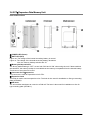
Before You Start
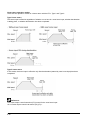
Operating environment
(Use the unit within the range of the general specifications when installing)
-Ambient temperatures:0 ~ +55 °C
-Ambient humidity: 30% to 85% RH (at 25°C, non-condensing)
-Keep the height below 2000m.
-For use in pollution Degree 2 environment.
-Do not use it in the following environments.
- Direct sunlight
- Sudden temperature changes causing condensation.
- Inflammable or corrosive gas.
-Excessive airborne dust, metal particles or saline matter.
- Benzine, paint thinner, alcohol or other organic solvents or strong alkaline solutions such as ammonia
or caustic soda.
-Direct vibration, shock or direct drop of water.
- Influence from power transmission lines, high voltage equipment, power cables, power equipment,
radio transmitters, or any other equipment that would generate high switching surges.(100mm or
more)
Static electricity
- Do not touch connector pins directly to prevent static electricity from causing damage.
- Always rid yourself of any static electricity before handling this product.
Power supplies
-Twist the wires of the power supply.
-The unit has sufficient noise immunity against the noise generated on the power line.
However, it is recommended to take measures for reducing noise such as using a isolating transformer
before supplying the power.
-Allocate an independent wiring for each power supplying line, input/output device and operating device.
-If using a power supply without a protective circuit, power should be supplied through a protective
element such as a fuse.
-Be sure to supply power to a control and an expansion units from a single power supply.
Turning on/off of the power of all the units must be conducted simultaneously.
Power supply sequence
In order to protect the power supply sequence, make sure to turn off the control unit before the
input/output power supply. If the input/output power supply is turned off before the control unit, or if the
control unit is not shut off momentarily, the controller detects change of input level, and might conduct an
unexpected operation
Before turning on the power
When turning on the power for the first time, be sure to take the precautions given below.
-When performing installation, check to make sure that there are no scraps of wiring,
particularly conductive fragments, adhering to the unit.
-Verify that the power supply wiring, I/O wiring, and power supply voltage are all correct.
-Sufficiently tighten the installation screws and terminal screws.
-Set the mode selector to PROG. Mode.
v
Before entering a program
-Be sure to perform a program clear operation before entering a program.
-For information on the operating procedure, refer to the manuals of tool software.
(Tool software: FPWIN Pro, FPWIN GR)
Request concerning program storage
To prevent the accidental loss of programs, the user should consider the following measures.
-Drafting of documents
To avoid accidentally losing programs, destroying files, or overwriting the contents of a file,
documents should be printed out and then saved.
-Specifying the password carefully
The password setting is designed to avoid programs being accidentally overwritten. If the password is
forgotten, however, it will be impossible to overwrite the program even if you want to.
Also, if a password is forcibly bypassed, the program is deleted. When specifying the password,
note it in the specifications manual or in another safe location in case it is forgotten at some point.
Battery
Do not install the battery when it is not used.
There is a possibility of leak if the battery remains discharged.
vi
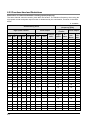
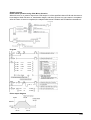
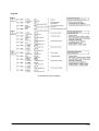
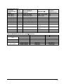
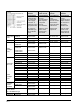
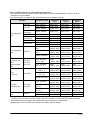
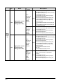
Differences in Functions Between Versions of
Controller
Usable model
Version
V1.11
V1.20
V1.24
V1.30
12k type
V1.40
V1.50
V2.00
V2.01
V2.10
12k type
V2.40
V2.50
32k type
V3.00
Usable functions
Addition of F174(SP0H) instruction
By SYS1 instruction
Detection edge setting for external input interrupt
MEWTOCOL-COM Response time setting
Writing into DT90014, DT90037, DT90038 by F0(MV) instruction
Operand and index modification by F12(ICRD)/P13(ICWT) instruction
Shortening of polling cycle by MEWTOCOL-COM during 1:N
communication
Setting for dealing the previous value of DF instruction in the system
register 4th bit D and MC
60-step acceleration/deceleration by F171(SPDH) instruction
Target value match stop mode by F172(PLSH) instruction
R9005 and R9006 is always announced when the battery error occurs.
Change in the detection timing of the battery error. It is detected 2
seconds after the power is on.
Left expansion refresh is available.
Operand and index modification by F12(ICRD)/P13(ICWT) instruction
Shortening of polling cycle by MEWTOCOL-COM during 1:N
communication
Setting for dealing the previous value of DF instruction in the system
register 4th bit D and MC
R9005 and R9006 is always announced when the batter error occurs.
Change in the detection timing of the battery error. It is detected 2
seconds after the power is on.
Interrupt program can be started when the high-speed counter target
value matches.
Scan time display in 100us unit
10us ring counter DT90020
General-purpose communication function with TOOL port
MODBUS-RTU master/slave communication function (COM1, COM2)
MEWTOCOL-COM master communication function (COM1, COM2)
32k-step program capacity
Enhancement of comment capacity
Enhancement of security functions
If failed to input a correct 4-digit password for 3 times in succession,
the operation cannot be continued.
8-digit password
Prohibition of program readout
Forced cancel of security
Reading of security information
Reverse setting function of PC link (32k type only)
R9005 and R9006 is always announced when the battery error occurs.
Change in the detection timing of the battery error. It is detected 2
seconds after the power is on.
Real number basic compare instructions 18 types
STF=S1, S2
ANF=S1, S2
ORF=S1, S2
STF<>S1, S2
ANF<>S1, S2
ORF<>S1, S2
STF>S1, S2
ANF>S1, S2
ORF>S1, S2
STF>=S1, S2
ANF>=S1, S2
ORF>=S1, S2
STF<S1, S2
ANF<S1, S2
ORF<S1, S2
STF<=S1, S2
ANF<=S1, S2
ORF<=S1, S2
vii
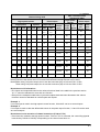
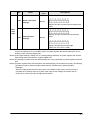
Usable model
32k type
32k type
Version
V3.00
V3.10
Usable functions
<Special instructions>
F230 (TMSEC)
F231 (SECTM)
F354 (FSCAL)
<Serial data conversion>
F250 (BTOA) Binary → ASCII conversion
F251 (ATOB) ASCII → Binary conversion
<SYS instructions>
UP/DOWN switching of HSC by SYS1 instruction
Addition of 8-digit password operation by SYS1 instruction
Addition of operation by SYS2 instruction
MODBUS master instructions
F145 (SEND) Data send
F146 (RECV) Data receive
MEWTOCOL master instructions
F145 (SEND) Data send
F146 (RECV) Data receive
F356 (EZPID) Easy PID instructions
<Partial I/O refresh>
Partial I/O refresh for FP0 expansion
<10us ring counter current value read>
F0 (MV) DT90020, D
<New PID instruction>
F356 (EZPID)
F182(FILTR) Time constant processing
Sampling trace function (Refer to Chapter 9.)
Sampling by instructions
F155(SMPL) Sampling
F156(STRG) Sampling trigger
Sampling by specifying time
Leading contact, trailing contact instructions
ST↑ AN↑ OR↑
ST↓ AN↓ OR↓
An arbitrary device can be specified for the setting value of
Timer/counter instruction.
e.g.) TML 0, DT0
Other additional convenient instructions
F252(ACHK) ASCII data check
F284(RAMP) Inclination output
Baud rate setting (300, 600, 1200 bps) by SYS instruction
High-speed operation
F0(MV) and F1(DMV) instructions Execution time: Approx. 1us
Only when every operands are without index modifier.
Function addition to existing instructions
F70(BCC) Block check code calculation
F356(EZPID) Easy PID instruction
Reference: <Programming Manual ARCT1F313E>
viii
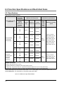
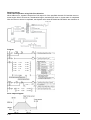
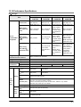
Programming Tool Restrictions
Type of programming tool
FPG-C32T
FPT-C32TTM
Type of unit
FPG-C32T2
FPG-C28P2
FPG-C24R2
FPG-C32TH
FPG-C32T2TM FPG-C32THTM
FPG-C28P2TM
FPG-C24R2TM
Used
Used
(Ver. 2.6 or
(Ver. 2.1 or
later)
later)
FPG-C32T2H
FPG-C28P2H
FPG-C24R2H
FPG-C32T2HTM
FPG-C28P2HTM
FPG-C24R2HTM
Used
(Ver. 2.6 or
later)
FPWIN GR
Ver.2
Used
FPWIN GR
Ver.1
Not used
Not used
Not used
Not used
Windows
software
Conforms to
IEC61131-3
FPWIN Pro
Ver.6
Used
Used
Used
Used
Not used
Not used
Not used
Not used
Handy
programming
unit
AFP1113V2
AFP1114V2
AFP1113
AFP1114
AFP1111A
AFP1112A
AFP1111
AFP1112
Not used
Not used
Not used
Not used
Not used
Not used
Not used
Not used
Windows
software
Note: Precautions concerning version upgrade
- In case of using FPWIN GR Ver.1, please purchase upgrade model FPWIN GR Ver.2.
- FPWIN GR Ver. 2.0 can be upgraded to Ver. 2.1 or later free of charge at our web site.
- FPWIN Pro Ver. 6.0 can be upgraded to Ver. 6.1 or later free of charge at our web site.
Website address: http://industrial.panasonic.com/ac/e/dl_center/software/
ix
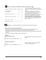
Changing Program from 12k Type to 32k Type
Program compatibility
- Between the 12k type and the 32k type, the number of internal relays and the hold type areas backed
up in the F-ROM area when the power turns off differ as the figure shown below.
- When a battery for memory backup is used, the hold type area can be set by system registers
regardless of the areas shown below.
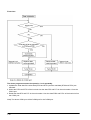
Procedure for changing program type
As a program that has been converted cannot be converted inversely, back up the program before
conversion.
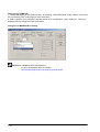
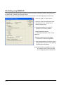
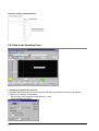
1. Retrieve a program to be converted with FPWIN GR.
2. Select "Tool" > "Change PLC Type" in the menu bar.
The "Select PLC Type" dialog box appears.
3. Select "FP SIGMA 32K" and press the "OK" button.
The type conversion wizard appears.
x
4. Press the "Next" button.
The menu for selecting "Initialize system register No. 7" is displayed.
Selection
Value of system register No.7
Starting word No. of internal
relay hold area
Initialize
248
Not initialize
90
Non-hold/hold type setting after conversion
Non-hold area
Hold area
WR0 to WR247
(R0 to R247F)
WR0 to WR89
(R0 to R89F)
WR248 to WR255
(R2480 to R255F)
WR90 to WR255
(R900 to R255F)
Note:
- When a memory backup battery is not used, select "Initialize" in the above wizard. If "Not initialize" is
selected, the value of data in the hold area may be indefinite.
5. Select "Initialize" or "Not initialize", and press the "Next" button.
The menu for selecting a "program conversion method" is displayed. See the next page for the examples
of conversion methods.
6. Select a program conversion method and press the "Execute" button.
The program is converted by the specified method and a message indicating that the conversion was
completed is displayed.
xi
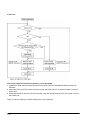
Key Point:
The results of various conversions when the following program of FPΣ (12k) type is converted
are shown below.
1 When selecting "Add transfer program automatically";
○
- Programs for transferring internal relays in the hold type area are inserted before and after the program
before conversion.
- The internal relay numbers in the program before conversion are not converted.
- As program compatibility is retained, for accessing corresponding internal relays from an external
device such as a programmable display, it is not necessary to change the settings of the external
device.
2 When selecting "Convert internal relay No. automatically";
○
- Only internal relay numbers are converted.
- Internal relays WR90 to WR97 in the program before conversion are converted to WR248 to WR255.
- For accessing corresponding internal relays from an external device such as a programmable display, it
is necessary to change the settings of the external device.
3 When selecting "Not change";
○
- Both program and internal relay numbers are not converted.
xii
Detail of conversion when selecting "Add transfer program automatically"
- Compatibility can be retained with the existing program by partially adding a transfer program without
modifying the existing program.
- Also, for connecting a device such as a programmable display, it is not necessary to change switches
and internal relays R and WR referred by data parts on the programmable display.
<Explanation of program>
○
1 Beginning of a program
Transfers the contents stored in the hold area of internal relays (WR248 to WR255) to the existing hold
area (WR90 to WR97) when the power turns on, and returns the area (WR90 to WR97) to the previous
state before the power turns off.
(because the area WR90 to WR97 cannot be held without a battery on V3.)
○
2 End of a program
After returning to the previous state that is the one before the power turns off, always transfers the WR
operated during the scan or the information of R input from a programmable display (WR90 to WR97) to
the hold area (WR248 to WR255). And prepares for holding data when the power turns off.
xiii
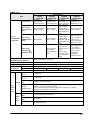
Compatibility with FP0
Program compatibility
The following points require attention if using FP0 programs on the FPΣ.
• Pulse output function
With the FPΣ, please be aware that the following changes have been made to instructions
concerning pulse output.
Instruction
For FP0
For FPΣ
Trapezoidal control
F168(SPD1)
F171(SPDH)
Jog feed
F169(PLS)
F172(PLSH)
Data table control
None
F174(SP0H)
Note1)
Linear interpolation control
None
F175(SPSH)
Note1)
Circular interpolation control
None
F176(SPCH)
PWM output
F170(PWM)
F173(PWMH)
Availability of linear and circular interpolation control is limited depending on the types of FPΣ Control
Unit.
Type
C32/C32TH
C32H/C32HTM
C32T2/C32T2TM
C32T2H/C32T2HTM
C28P2/C28P2TM
C28P2H/C28P2HTM
C24R2/C24R2TM
C24R2H/C24R2HTM
Using F175, F176
Not available
Available
Available
Not available
• Serial data communication function
With the FPΣ, please be aware that the following changes have been made to instructions
concerning serial data communication.
Instruction
For FP0
For FPΣ
Note2)
Serial data communication
F144(TRNS)
F159(MTRN)
Note) The F159 (MTRN) instruction is used only with an FPΣ in which the conventional F144 (TRNS)
instruction has been set up to correspond to multiple communication ports. Please be aware that
the conventional F144 (TRNS) instruction cannot be used with the FPΣ.
xiv
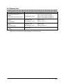
Manuals to be Used
Necessary manuals vary according to the unit used. Check the following table and prepare required
manuals.
Unit type
User's Manual
Programming Manual
Exclusive manual
ARCT1F333E
ARCT1F353E
FPΣ Control unit
Yes
Yes
FPΣ Expansion I/O unit
Yes
Yes
No
FPΣ Positioning unit
Yes
Yes
ARCT1F365E
FPΣ Expansion
Yes
Yes
No
data memory unit
FPΣ CC-Link slave unit
Yes
Yes
ARCT1F380E
FPΣ S-LINK unit
Yes
Yes
ARCT1F403E
FPΣ Communication
Yes
Yes
No
cassette
Key Point:
• As for requesting for manuals, please contact your dealer or download the PDF data from our web site.
• http://industrial.panasonic.com/ac/e/dl_center/manual/ (User registration is required. Free of charge)
xv
xvi
Chapter 1
Functions and Restrictions of the Unit
1.1 Features and Functions of the Unit
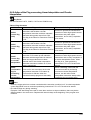
Powerful control capabilities
All of the functions of a mid-scale PLC are packed into the compact body size of the 32-pont type FP0. A
program capacity of 12k steps or 32k steps is provided as a standard feature, so you never have to
worry about how much memory is left as you’re programming. In addition, 32k words are reserved for
data registers, so large volumes of data can be compiled and multiple operations can be processed
without running out of memory.
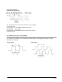
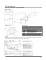
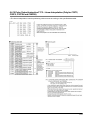
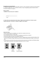
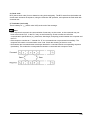
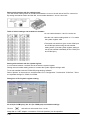
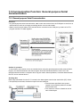
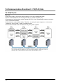
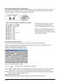
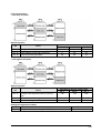
A full range of communication functions
Using the Tool port (RS232C) provided as a standard feature on the main unit, communication can be
carried out with a display panel or computer. Additionally, communication cassettes with RS232C and
RS485 interfaces are available as an option. Installing a 2-channel RS232C type communication
cassette in the FPΣ makes it possible to connect two devices with RS232C port. A full lineup of
communication functions means you can also work with 1:N communication (up to 99 units) and
PC(PLC) link function (up to 16 units).
Controlling two devices with RS232C port with one FPΣ
When using the 2-channel RS232C type communication cassette
1:N communication possible with up to 99 stations (units)
When using the 1-channel RS485 type communication cassette
When using the 1-channel RS485 and 1-channel RS232C in combination
1-2
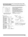
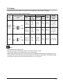
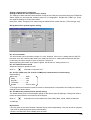
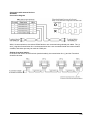
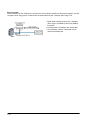
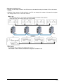
Data can be share among the various PLCs using the PC(PLC) link function
When using the 1-channel RS485 type communication cassette
When using the 1-channel RS485 and 1-channel RS232C combination type
PC(PLC) link function (up to 16 units) or 1:N communication (up to 99 units) with RS232C devices
When using the 1-channel RS485 and 1-channel RS232C in combination
Analog control supported
An analog potentiometer (volume dial) is provided as a standard feature. This can be used in
applications such as analog timers, without using the programming tools. An analog unit is also available
as the intelligent unit.
Type with thermister input function
For the units of which part numbers or product numbers end in “TM”, the leader line which enables the
thermister input is equipped instead of an analog potentiometer. The change of the resistance value of
the thermister can be taken in as an analog value.
(The thermister of which resistance value is from 200 to 75 kΩ can be used.)
Calender timer function can be added
Optional backup battery enables the calender timer function.
1-3
Positioning control supported through high-speed counter and pulse output
A high-speed counter and pulse output functions are provided as standard features. The pulse output
function supports frequencies of up to 100kHz, enabling positioning control using a stepping motor or
servo motor.
Measurement using high-speed counter supported
Increment input mode, decrement input mode, 2-phase input mode, individual input mode, and direction
discrimination mode are supported.
Positioning control based on pulse output supported
Pulse/direction and clockwise/counter –clockwise output are supported.
Heater control based on PWM output function supported
The pulse output at any duty ratio can be picked up with special instruction.
1-4
Security functions have been enhanced.
1. Upload protection. (Enables not to upload programs.)
2. 8-digit alphameric password
3. 4-digit numeric password
Easy temperature control instruction has been added.
It enables to perform the operation easily like a temperature control device.
Single-line PID instruction has been added.
Three-port general purpose serial communication
The tool port also supports the general-purpose serial communication.
Modbus RTU master unit and slave units
Communication with a temperature control device, inverter or measuring instruments can be performed
with simple programs using the FPΣ as a master unit.
Communication with the existing network can be performed using the FPΣ as slave units.
MEWTOCOL master unit
Programs for the MEWTOCOL communication master unit can be easily created.
Rewrite function during RUN
Programs can be changed during RUN up to 512k steps.
1-5
1.2 Unit Types
1.2.1 FPΣ Control Units
12k type (Products discontinued as of May 2008)
Name
Number of I/O points
Part No.
Product No.
Input: 16 points/Transistor output: 16
FPG-C32T
AFPG2543
points NPN
Input: 16 points/Transistor output: 16
FPG-C32T2
AFPG2643
points NPN
FPΣ Control unit
Input: 16 points/Transistor output: 12
FPG-C28P2
AFPG2653
points PNP
Input: 16 points/Relay output: 8 points
FPG-C24R2
AFPG2423
Input: 16 points/Transistor output: 16
FPG-C32TTM
AFPG2543TM
points NPN
Input: 16 points/Transistor output: 16
FPΣ Control unit
FPG-C32T2TM
AFPG2643TM
With thermister input points NPN
function
Input: 16 points/Transistor output: 12
FPG-C28P2TM
AFPG2653TM
points PNP
Input: 16 points/Relay output: 8 points
FPG-C24R2TM
AFPG2423TM
Note) The FPΣ expansion I/O unit cannot be added to FPG-C32T nor FPG-C32TTM FPΣ control unit.
32k type
Name
FPΣ Control unit
(High capacity type)
Program capacity: 32k
Number of I/O points
Input: 16 points/Transistor output: 16
points NPN
Input: 16 points/Transistor output: 16
points NPN
Input: 16 points/Transistor output: 12
points PNP
Input: 16 points/Relay output: 8 points
Input: 16 points/Transistor output: 16
points NPN
Input: 16 points/Transistor output: 16
points NPN
Input: 16 points/Transistor output: 12
points PNP
Part No.
Product No.
FPG-C32TH
AFPG2543H
FPG-C32T2H
AFPG2643H
FPG-C28P2H
AFPG2653H
FPG-C24R2H
AFPG2423H
FPGAFPG2543HTM
C32THTM
FPΣ Control unit
FPGAFPG2643HTM
(High capacity type)
C32T2HTM
Program capacity: 32k
FPGWith thermister input
AFPG2653HTM
C28P2HTM
function
FPGInput: 16 points/Relay output: 8 points
AFPG2423HTM
C24R2HTM
Note) The FPΣ expansion I/O unit cannot be added to FPG-C32TH nor FPG-C32THTM FPΣ control unit.
1-6
1.2.2 FPΣ Expansion Units
Name
FPΣ Expansion
I/O unit
FPΣ
Positioning unit
FPΣ
Positioning unit
RTEX
FPΣ S-LINK unit
FPΣ CC-Link
slave unit
Specifications
Input: 32 points/Transistor
output: 32 points NPN
Input: 32 points/Transistor
output: 32 points PNP
Transistor output: 1-axis type
Transistor output: 2-axis type
Line driver output: 1-axis type
Line driver output: 2-axis type
2-axis type
4-axis type
8-axis type
128 input/output points using
S-LINK
Number of points of
exchanged data with CC-Link
master station
Max. 224 points (Input: 112
points, output: 112 point)
Writing max. 16-word data
Reading 4-word data
Part No.
Product No.
Manual
FPG-XY64D2T
AFPG3467
FPG-XY64D2P
AFPG3567
FPG-PP11
FPG-PP21
FPG-PP12
FPG-PP22
FPG-PN2AN
FPG-PN4AN
FPG-PN8AN
AFPG430
AFPG431
AFPG432
AFPG433
AFPG43610
AFPG43620
AFPG43630
FPG-SL
AFPG780
ARCT1F403E
FPG-CCLS
AFPG7943
ARCT1F380E
This manual
ARCT1F365E
ARCT1F421E
FPΣ Expansion
256 kbyte
FPG-EM1
AFPG201
This manual
data memory unit
Note) The FPΣ expansion I/O unit cannot be added to FPG-C32T nor FPG-C32TTM FPΣ control unit.
1-7
1.2.3 FP0R Expansion Units
Specifications
Product
name
FP0R-E8
Expansion
Unit
FP0R-E16
Expansion unit
FP0R-E32
Expansion unit
1-8
No. of I/O points
Power
supply
voltage
Input
Output
8 points
(Input: 8 points)
-
24V DC
±common
-
8 points
(Input: 4 points,
Output: 4 points)
24V
DC
24V DC
±common
Relay output:
2A
8 points
(Output: 8 points)
24V
DC
-
8 points
(Output: 8 points)
-
-
8 points
(Output: 8 points)
-
-
16 points
(Input: 16 points)
-
24V DC
±common
-
16 points
(Input: 8 points,
Output: 8 points)
24V
DC
24V DC
±common
Relay output:
2A
-
24V DC
±common
-
24V DC
±common
16 points
(Output: 16 points)
-
-
16 points
(Output: 16 points)
-
-
-
24V DC
±common
-
24V DC
±common
16 points
(Input: 8 points,
Output: 8 points)
16 points
(Input: 8 points,
Output: 8 points)
32 points
(Input: 16 points,
Output: 16 points)
32 points
(Input: 16 points,
Output: 16 points)
Relay output:
2A
Transistor
output: (NPN)
0.3A
Transistor
output: (PNP)
0.3A
Transistor
output: (NPN)
0.3A
Transistor
output: (PNP)
0.3A
Transistor
output: (NPN)
0.3A
Transistor
output: (PNP)
0.3A
Transistor
output: (NPN)
0.3A
Transistor
output: (PNP)
0.3A
Connection
type
MIL
connector
Terminal
block
Molex
connector
Terminal
block
Product No.
AFP0RE8X
AFP0RE8RS
AFP0RE8RM
AFP0RE8YRS
MIL
connector
AFP0RE8YT
MIL
connector
AFP0RE8YP
MIL
connector
Terminal
block
Molex
connector
AFP0RE16X
AFP0RE16RS
AFP0RE16RM
MIL
connector
AFP0RE16T
MIL
connector
AFP0RE16P
MIL
connector
AFP0RE16YT
MIL
connector
AFP0RE16YP
MIL
connector
AFP0RE32T
MIL
connector
AFP0RE32P
1.2.4 FP0 Intelligent Units
Product name
FP0 A/D
converter unit
FP0
Thermocouple
unit
FP0 RTD
(Resistancetemperature
detector) unit
FP0 Analog I/O
unit
FP0 D/A
converter unit
Specifications
Part No.
Product No.
Manual
<Input specifications>
No. of channels: 8 channels
Input range: Voltage: 0 to 5 V, -10 to +10 V,
-100 to 100 mV
(Resolution: 1/4000)
Current: 0 to 20 mA (Resolution: 1/4000)
FP0-A80
AFP0401
K, J, T, R thermocouples, resolution: 0.1°C
FP0-TC4
AFP0420
K, J, T, R thermocouples, resolution: 0.1°C
FP0-TC8
AFP0421
Pt100, Pt1000, Ni1000
Resolution: 0.1°C/0.01°C (Switch type)
FP0-RTD6
AFP0430
ARCT1F445
FP0-A21
AFP0480
ARCT1F390
FP0-A04V
AFP04121
<Input specifications>
No. of channels: 2 channels
Input range: Voltage: 0 to 5V, -10 to +10V
(Resolution: 1/4000)
Current: 0 to 20 mA (Resolution: 1/4000)
<Output specifications>
No. of channels: 1 channel
Output range: Voltage: -10 to +10V (Resolution:
1/4000)
Current: 0 to 20 mA (Resolution: 1/4000)
<Output specifications>
No. of channels: 4 channels
Output range: (Voltage output type): -10 to +10V
(Resolution: 1/4000)
(Current output type): 4 to 20 mA (Resolution:
1/4000)
ARCT1F321
ARCT1F366
ARCT1F382
FP0-A04I
AFP04123
1.2.5 FPΣ Communication Cassette
Name
FPΣ Communication
cassette 1-channel
RS232C type
FPΣ Communication
cassette 2-channel
RS232C type
FPΣ Communication
cassette 1-channel
RS485 type
FPΣ Communication
cassette 1-channel
RS485 type & 1-channel
RS232C type
Description
This communication cassette is a 1-channel unit
with a five-wire RS232C port. RS/CS control is
possible.
This communication cassette is a 2-channel unit
with a three-wire RS232C port. Communication
with two external devices is possible.
This communication cassette is a 1-channel unit
with a two-wire RS485 port.
This communication cassette is a 1-channel unit
with a two-wire RS485 port and a 1-channel unit
with a three-wire RS232C port.
Part No.
Product No.
FPG-COM1
AFPG801
FPG-COM2
AFPG802
FPG-COM3
AFPG803
FPG-COM4
AFPG806
1-9
1.2.6 Link Units
Power
supply
voltage
Part No.
Product
No.
Product name
Specifications
Manual
FP0 I/O Link unit
This is a link unit designed to
make the FP0 function as a slave
unit to MEWNET-F (remote I/O
system).
24V DC
FP0-IOL
AFP0732
This manual
FP0 CC-Link
Slave unit
This unit is for making the FP0
function as a slave unit of the CCLink. Only one unit can be
connected to the furthest right
edge of the FP0 expansion bus.
Note) Accuracy will change if an
FP0 thermocouple unit is used at
the same time.
24V DC
FP0-CCLS
AFP07943
ARCT1F380
C-NET Adapter
S2 type
(for PLC tool port
side)
This is an RS485 adapter
designed to allow use of the
computer link function for
connecting to a host computer via
C-NET. It comes with a cable (30
cm) for tool port side. A power
supply is not required.
-
-
AFP15402
C-NET Adapter
(For computer
side)
This is an RS485 adapter
designed to allow use of the
computer link function for
connecting to a networkconnected PLC via C-NET from a
host computer.
FP Web-Server2
unit
This is a unit to conduct Ethernet connection for
FP series PLCs and RS232C devices. It is
equipped with web and mail functions.
ARCT1F96
100 to 240V
AC
-
AFP8536
24V DC
-
AFP8532
FP-WEB2
AFP0611
ARCT1F446
Part No.
Product No.
1.2.7 Power Supply Unit
Product name
FP0 Power
supply unit
1-10
Specifications
Input voltage: 100 to 240 VAC Free input
Output capacity: 0.7 A, 24 VDC
FP0-PSA4
AFP0634
1.2.8 Options
Product name
Options
for
memory
backup
Backup battery
for FPΣ
High-capacity
battery folder for
FPΣ
FP Memory loader
FP0
Mounting
plate
Wiring
tools
Specifications
Necessary for the backup of data
registers, etc. or for using the
clock/calendar function.
Programming tool for copying
programs written to a control unit
Product No.
With a connector
AFPG804
Folder with a connector
for a commercial battery
CR123A
AFPG807
(Folder only)
Data clear type
AFP8670
Data hold type
AFP8671
Slim 30 type
Mounting plate for mounting FPΣ Control unit or FPΣ Expansion
I/O unit on a panel vertically.
AFP0811
(10-pack)
Slim type
Mounting plate for mounting FP0/FP0R Expansion unit or
Intelligent unit on a panel vertically.
AFP0803
(10-pack)
Flat type
Mounting plate for mounting FPΣ Control unit on a panel
horizontally.
AFP0804
(10-pack)
Terminal
screwdriver
Required for connecting the terminal block (made by Phoenix
Contact Co.) supplied with FPΣ Control unit (relay output type).
AFP0806
Multi-wire
connector
pressure contact
tool
Required for connecting the connectors supplied with FPΣ
Control unit (transistor type) or FPΣ Expansion I/O unit.
AXY52000FP
Flat cable
connector
Required for wiring with flat
cables.
I/O cable
For FPΣ Control unit (transistor output type) and
FP0R Expansion unit. Loose-wiring cable, with
connector attached at one end.
10 leads, AWG22 (0.3mm2), 2 pcs (blue and
white) /set.
For FPΣ Control unit
(transistor output type), 10P
AFP0808
(4-pack)
For FPΣ Expansion I/O unit,
40P
AFP2802
(2-pack)
Length: 1 m
AFP0521
(2 cable set)
Length: 3m
AFP0523
(2 cable set)
Note) For using the high-capacity battery folder for FPΣ, purchase a commercial CR123A battery.
1.2.9 Maintenance Parts
Product name
Terminal socket
Wire-press socket
Specifications
Product No.
Attaches to FPΣ control unit (relay output type). 9P
AFP0802 (2-pack)
Attaches to FPΣ control unit (transistor output type). 10P
AFP0807 (2-pack)
Attaches to FPΣ expansion I/O unit and FPΣ positioning
unit. 40P
AFP2801 (2-pack)
Suitable wire: AWG #22/
AWG #24
AXW7221FP
(5 pins in line)
Suitable wire: AWG #26/
AWG #28
AXW7231FP
(5 pins in line)
Wire-press contact
For FPΣ control unit (transistor
output type), FPΣ expansion
I/O unit and FPΣ positioning
unit.
Power cable for FP0R/FPΣ
Attaches to FP0R/FPΣ control unit. Length: 1 m
AFPG805 (1-pack)
Power cable for FP0
Attaches to FP0/FP0R expansion unit. Length: 1 m
AFP0581 (1-pack)
Note) Order wire-press contacts in units of 200 pins in 40 rows.
1-11
1.3 Restrictions on Unit Combinations
1.3.1 Restrictions on FP0 Expansion Unit
Up to three expansion units can be added on the right of the FPΣ, these expansion units being either
expansion units or intelligent units from the earlier FP0 series, or a combination of the two.
A combination of relay output types and transistor output types is also possible.
Controllable I/O points
Number of I/O points when
Number of I/O points when
using control unit
using FP0 expansion unit
FPG-C32
32 points
Max. 128 points
FPG-C28
28 points
Max. 124 points
Note1)
FPG-C24
24 points
Max. 120 points
Note1) This is the number of points when combining with the transistor type FP0 expansion unit.
Type of control unit
Note:
• Install the FP0 thermocouple unit on the right side of all other expansion units. If it is installed on the
left side, the total precision will deteriorate.
• Install the FP0 CC-Link slave unit on the right side of the other expansion units. There is no expansion
connector on the right side.
• Install the FP0 RTD unit on the right side of the other expansion units.
1-12
1.3.2 Restrictions on FPΣ Expansion Unit
Up to four dedicated FPΣ expansion units can be added on the left of the FPΣ.
The 64 points type expansion unit consists of 32 input points and 32 transistor NPN output points.
Controllable I/O points
Number of I/O points when
Number of I/O points when
using control unit
using FPΣ expansion unit
Note1)
Note2)
FPG-C32
32 points
Max. 128 points
Note2)
FPG-C28
28 points
Max. 124 points
FPG-C24
24 points
Max. 120 points
Note1) The FPΣ cannot be used for FPG-C32T, FPG-C32TTM, FPG-C32TH nor FPG-C32THTM.
Note2) This is the number of points when combining with the 64-point type FPΣ expansion unit.
Type of control unit
Key Point:
If using FP0 expansion units and FPΣ expansion units in combination, the number of input and output
points can be expanded to a maximum of 384 points for FPG-C32T2 and FPG-C32T2TM.
1-13
1.4 Programming Tools
1.4.1 Tools Needed for Programming
1. Programming tool software
• The tool software can also be used with the FP
series.
• “FPWIN Pro Ver.6” or “FPWIN GR Ver.2”
Windows software is used with FPΣ.
See Also: Programming Tool Restrictions
2. PC connection cable
• The connection cable is available.
1.4.2 Software Environment and Suitable Cable
Standard ladder diagram tool software FPWIN-GR Ver.2
OS (Operating
Type of software
system)
Windows98
WindowsMe
Full type
FPWIN GR Ver.2
Windows2000
English-language
WindowsXP
menu
Upgrade version Windows Vista
Hard disk
capacity
Product No.
AFPS10520
40MB or more
AFPS10520R
Windows7
Note1) Ver.1.1 must be installed to install the upgrade version.
Note2) Ver.2.0 can be upgraded to Ver. 2.1 or later free of charge at our web site
(http://industrial.panasonic.com/ac/e/dl_center/software/).
Conforms to IEC61131-3 programming tool software FPWIN-Pro Ver.6
Type of software
OS (Operating system)
Hard disk capacity
FPWIN Pro Ver.6
English-language menu
Windows2000
WindowsXP
Windows Vista
Windows7
100MB or more
Product No.
FPWINPROFEN6
Note1) Ver.6.0 can be upgraded to Ver. 6.1 or later free of charge at our web site
(http://industrial.panasonic.com/ac/e/dl_center/software/).
Type of computer and suitable cable
Connector
Specifications
D-sub 9-pin female-Mini DIN round 5-pin
D-sub 9-pin
D-sub 0-pin female-Mini DIN round 5-pin straight type
1-14
Product No.
AFC8503
AFC8503S
Chapter 2
Specifications and Functions of the Unit
2.1 Parts and Functions
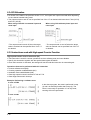
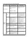
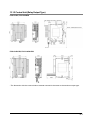
① Status indicator LEDs
These LEDs display the current mode of operation or the occurrence of an error.
LED
LED and operation status
Lights when in the RUN mode and indicates that the program is being executed.
RUN (green)
It flashes during forced input/output. (The RUN and PROG. LEDs flash
alternately.)
Lights when in the PROG. Mode and indicates that operation has stopped.
PROG. (green)
ERROR/ALARM
(red)
2-2
Lights when in the PROG. Mode during forced input/output.
It flashes during forced input/output. (The RUN and PROG. LEDs flash
alternately.)
Flashes when an error is detected during the self-diagnostic function. (ERROR)
Lights if a hardware error occurs, or if operation slows because of the program,
and the watchdog timer is activated. (ALARM)
② RUN/PROG. mode switch
This switch is used to change the operation mode of the PLC.
Switch position
Operation mode
This sets the RUN mode. The program is executed is executed and operation
RUN (upward)
begins.
This sets the PROG. mode. The operation stops. In this mode, programming
PROG. (downward)
can be done using tools.
• The remote switching operation from the programming tool is operable.
• When performing remote switching from the programming tool, the setting of the mode switch and the
actual mode of operation may differ. Verify the mode with the status indicator LED.
• Restart FPΣ to operate in the mode set with the RUN/PROG. mode switch.
③ Communication status LEDs
These LEDs display the communication status of the COM.1 and COM.2 ports.
LED
LED and communication status
Flashes while data is being transmitted.
Transmitted
S
data monitor
Goes out when no data is being transmitted.
COM.1
Flashes while data is being received.
Received
R
data monitor
Goes out when no data is being received.
Flashes while data is being transmitted.
Transmitted
(In case of 1-channel RS232C1 type, lights when the RS signal is ON.)
S
data monitor
Goes out when no data is being received.
COM.2
Flashes while data is being received.
(In case of 1-channel RS232C1 type, lights when the CS signal
Received
R
is ON.)
data monitor
Goes out when no data is being received.
④ Tool port (RS232C)
This port is used to connect a programming tool.
A commercial mini-DIN 5-pin connector is used for the Tool port on the control unit.
Pin No.
Signal name
Abbreviation
Signal direction
1
Signal Ground
SG
2
Transmitted Data
SD
Unit → External device
3
Received Data
RD
Unit ← External device
4
(Not used)
5
+5V
+5V
Unit → External device
• The followings are the default settings set when the unit is shipped from the factory. The system
register should be used to change these.
- Baud rate …….. 9600 bps
- Character bit …. 8 bit
- Parity check ….. Odd parity
- Stop bit length .. 1 bit
⑤ Input connector
⑥ Input indicator LEDs
⑦ Output connector
2-3
⑧ Output indicator LEDs
⑨ Analog potentiometer (analog dial)
(excluding the type of which part No. and product No. ends in TM)
Turning this dial changes the values of special data register DT90040 and DT90041 within the range of
K0 to K1000. It can be used for analog timers and other applications.
⑩ Power supply connector (24V DC)
Supply 24V DC. It is connected using the power supply cable (AFPG805) that comes with the unit.
⑪ Left-side connector for FPΣ expansion
This is used to connect dedicated FPΣ expansion unit on the left side of the control unit with the internal
circuit.
Note) FPG-C32T nor FPG-C32TTM control units are not equipped with this connector.
⑫ Unit No. (Station No.) setting switch
- The unit number setting switch is located under the left side cover of the unit. Unit numbers are set with
the switch and dial for using the communication function with an optional communication cassette.
- The switch is set to OFF and the dial is set to 0 at the factory, and the unit number setting is available
using system registers.
- When the switch is OFF and the dial is set to any of 1 to F, each unit number is 1 to 15. When the
switch is ON and the dial is set to any of 1 to F, each unit number is 16 to 31.
* Unit numbers can be set using system registers.
Note) The unit number of tool port cannot be set. Also, when using a 2-channel cassette, the both
channels are set to the same unit number. (Using system registers enables to set each unit number
individually.)
⑬ Communication cassette (option)
This is the optional cassette type adapter used when communication is carried out. Any one of the
following cassette types may be installed.
- 1-channel RS232C type
- 2-channel RS232C type
- 1-channel RS485 type
- 1-channel RS485 and 1-channel RS232C type in combination
2-4
⑭ Expansion hook
This hook is used to secure expansion units. The hook on the right side is also used for installation on
flat type mounting plate (AFP0804).
⑮ Right-side connector for FP0 expansion
This is used to connect an expansion unit to the internal circuit of the control unit.
(The connector is located under the seal.)
⑯ DIN hook
The FPΣ unit enables attachment at a touch to a DIN rail. The lever is also used for installation on slim
30 type mounting plate (AFP0811).
⑰ Battery cover
This is uncovered to mount the backup battery sold separately.
The backup of the calendar timer function or data register is possible with the backup battery.
⑱ Thermister input line (The end of part No. and product No. is TM type only)
It is used to connect the thermister to read the change in the resistance value of the thermister as analog
input values.
2-5
2.2 Input and Output Specifications
2.2.1 Input Specifications
Input Specifications (for all types)
Item
Description
Insulation method
Optical coupler
Rated input voltage
24V DC
Operating voltage range
21.6 to 26.4V DC
For X0, X1, X3, X4: approx. 8 mA
For X2, X5 to X7: approx. 4.3 mA
Rated input current
For X8 to XF: approx. 3.5 mA
For C32, C28: 16 points/common (X0 to XF/1 common)
For C24: 8 point/common (X0 to X7/1 common, X8 to XF/1
common)
Input points per common
(Either the positive or negative of the input power supply can be
connected to common terminal.)
For X0, X1, X3, X4: 19.2V DC/6 mA
Min. on voltage/Min. on current
For X2, X5 to XF: 19.2V DC/3 mA
Max. off voltage/Max. off current 2.4V DC/1.3 mA
For X0, X1, X3, X4: approx. 3 kΩ
For X2, X5 to X7: approx. 5.6 kΩ
Input impedance
For X8 to XF: approx. 6.8 kΩ
For input X0, X1, X3, X4:
1 ms or less: normal input
5 µs or less: high-speed counter, pulse catch, interrupt
Note1)
input settings
For input X2, X5 to X7:
off→on
1 ms or less: normal input
Response time
100µs or less: high-speed counter, pulse catch, interrupt
Note1)
input settings
For input X8 to XF
1 ms or less: normal input only
on→off
Same as above
Operating mode indicator
LED display
Note1) this specification is applied when the rated input voltage is 24V DC and the temperature is
25°C/70°F.
2-6
Limitations on number of simultaneous input on points
Keep the number of input points per common which are simultaneously on within the following range as
determined by the ambient temperature.
Circuit diagram
[X0, X1, X3, X4]
[X2, X5 to XF]
For X2, X5 to X7: R1=5.6kΩ R2=1kΩ
For X8 to XF:
R1=6.8kΩ R2=820Ω
2-7
2.2.2 Output Specifications
Transistor output specifications
Item
Insulation method
Output type
Rated load voltage
Operating load voltage range
Max. load current
Max. surge current
Output points per common
Off state leakage current
On state voltage drop
off→on
Response time
on→off
External power
Voltage
supply for driving
Current
internal circuit
Surge absorber
Operating mode indicator
Phase fault protection
Description
C32(NPN)
C28(PNP)
Optical coupler
Open collector
5 to 24V DC
24V DC
4.75 to 26.4V DC
21.6 to 26.4V DC
For Y0, Y1, Y3, Y4: 0.3A
For Y0, Y1, Y3, Y4: 0.5A
For Y2, Y5 to YF: 0.1A
For Y2, Y5 to YB: 0.3A
For Y0, Y1, Y3, Y4: 0.9A
For Y0, Y1, Y3, Y4: 1.5A
For Y2, Y5 to YF: 0.5A
For Y2, Y5 to YB: 0.7A
16 points/common
12 points/common
100µA or less
0.5V or less
For Y0, Y1, Y3, Y4 (at 15mA or less): 2µs or less
For Y2, Y5 or later: 0.2ms or less
For Y0, Y1, Y3, Y4 (at 15mA or less): 8µs or less
For Y2, Y5 or later: 0.5ms or less
21.6 to 26.4V DC
70mA or less
Zener diode
LED display
Phase fault protection, thermal protection for Y2, Y5 or later
Limitations on number of simultaneous output on points
Keep the number of output points per common which are simultaneously on within the following range as
determined by the ambient temperature.
2-8
Circuit diagram
[C32]
[Y0,Y1,Y3,Y4]
[C28]
[Y0,Y1,Y3,Y4]
[Y2, Y5 to YF]
[Y2, Y5 to YB]
2-9
Relay output specifications (C24)
Item
Description
Output type
1a output
Note1)
Rated control capacity
2A 250V AC, 2A 30V DC (4.5A per common or less)
Output points per common
8 points/common
off→on
Approx. 10ms
Response time
on→off
Approx. 8ms
Mechanical lifetime
Min. 20,000,000 operations
Electrical lifetime
Min. 100,000 operations
Surge absorber
None
Operating mode indicator
LED display
Note1) Resistance load
Limitations on number of simultaneous output on points
Keep the number of output points per common which are simultaneously on within the following range as
determined by the ambient temperature.
Circuit diagram
2-10
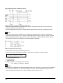
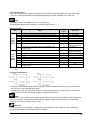
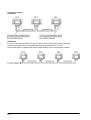
2.3 Terminal Layout Diagram
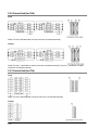
2.3.1 Control Unit (for C32)
Input
Note) The four COM terminals of input circuit are connected internally.
Output
Note) The two (+) terminals of output circuit are connected internally. The two (−) terminals of output
circuit are connected internally.
2-11
2.3.2 Control Unit (for C28)
Input
Note) The four COM terminals of input circuit are connected internally.
Output
Note) The two (+) terminals of output circuit are connected internally. The two (−) terminals of output
circuit are connected internally.
2.3.3 Control Unit (for C24)
Input
Note) The two COM terminals of input circuit are not connected internally.
Output
2-12
2.4 Analog Potentiometer
2.4.1 Overview of Analog Potentiometer
The FPΣ is equipped with two analog potentiometers as a standard feature. Turning the potentiometers
changes the values of the special data registers DT90040 and DT90041 within a range of K0 to K1000.
Using this function makes it possible to change the internal set values in the PLC without using the
programming tool, so this can be used, for example, with analog clocks, to change the set value
externally by turning the potentiometer.
Applicable special data register
Symbol
Potentiometer No.
V0
Volume 0
V1
Volume 1
Special data register
DT90040
DT90041
Range of change
K0 to K1000
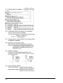
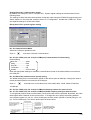
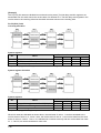
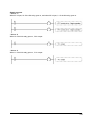
2.4.2 Example Showing How to Use Analog Potentiometer
The FPΣ is provided with special data registers, in which the values in the registers change in response
to the analog potentiometers being moved. If the values of these registers are sent to the clock setting
value area, a clock can be created that allows the time to be set using the potentiometer.
Example: Writing of the clock setting value
The value of the special data register (DT90040) that corresponds to the analog potentiometer V0 is sent
to the setting value area (SV0) of TMX0 to set the time for the clock.
2-13
2.5 Thermister Input (Only for TM type)
2.5.1 Overview of Thermister Input
The control units of which part and product numbers end in “TM” is equipped with the leader lines which
enable the thermister input instead of the analog potentiometer. The change in the termister’s resistance
values can be loaded as analog values by connecting the thermister with these leader lines.
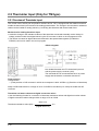
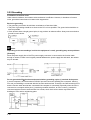
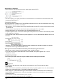
Mechanism for loading thermister input
• Loads the change in the resistance values of the thermister connected externally as the change in
voltage, and then loads it as digital values by the AD converter in which a microcomputer is built.
• The values converted to digital values are reflected in the special data registers (DT90040 or
DT90041) and can be read in the user’s program.
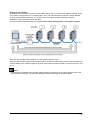
<Block diagram>
Non-isolated between the FPΣ thermister input unit
and the power supply connector (24V).
The red leader line is connected with the 3.3V power
supply and the black is connected with the Vin.
Total precision
Total precision
Note)
= (Total precision of AD converter in which microcomputer is built: ±5LSB
)+(Precision of thermister)
Note) ±5LSB means there is a margin of error of ±5LSB for the values (0 to 1000) converted with AD
converter.
Thermister resistance values and digital conversion values
• Use the following formula for conversion of thermister resistance values and digital conversion values.
• Digital conversion values changes within a range of K0 to K1000.
1024 X 2.2
Thermister resistance value (kΩ) =
-2.2
(Digital value+12)
2-14
Usable thermister
• Thermisters of which resistance values are within a range of 200Ω to 75kΩ.
Manufacturer
Thermister type (B constant)
Guide for Measuring range (°C)
3390 K
-50 to +100 °C
3450 K
50 to +150 °C
Shibaura
Electronics Co., Ltd.
4300 K
+100 to +200 °C
5133 K
+150 to +300 °C
Note:
• The length of the wiring between the FPΣ control unit and the thermister should be less than 10m.
• A thin wire (AWG28, length: 150 mm) is used for the leader line. Connect and bundle the wire without
any stress.
• It is recommended to mount parts such as condensers externally if the converted value is unstable.
2-15
2.5.2 Loading of Thermister Temperature Data
Reading the value of the FPΣ special data register enables to load the analog value data that
corresponds to the resistance value of the thermister.
Applicable special data register
Symbol
Thermister No.
V0
Thermister 0
V1
Thermister 1
Special data register
DT90040
DT90041
Digital value after conversion
K0 to K1000
Thermister measuring temperature – A/D conversion table (example: 3450K)
• Work out the temperature and the thermister resistance value from the temperature characteristic table
of the used thermister.
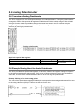
• The converted digital values can be calculated by the formula described in the previous page.
Thermister resistance
Converted digital
Temperature (°C)
Resolution (°C)
(kΩ)
value
50
4.3560
332
0.135
60
3.1470
409
0.130
70
2.3170
487
0.128
80
1.7340
561
0.135
90
1.3180
628
0.149
100
1.0170
688
0.167
110
0.7940
740
0.192
120
0.6277
785
0.222
130
0.5017
822
0.270
140
0.4052
853
0.323
150
0.3305
878
0.400
Note) (Total precision of AD converter in which microcomputer is built: ±5LSB)+(Precision of thermister)
is not included in the above digital values.
Conversion program using scaling instruction (F282)
• Appropriate data which interpolated from nonlinear data can be obtained by creating converted digital
values and temperature data as a data table and executing the scaling instruction (F282).
DT90040: Special data register
(Digital value after thermister input conversion)
DT0: Beginning of data table
DT100: Converted data (temperature)
Example of data table creation
Input data
Output data
(Converted digital value)
(Temperature)
DT0
11
DT1
332
DT12
50
DT2
409
DT13
60
DT3
487
DT14
70
•
•
•
•
•
•
•
•
DT11
878
DT22
150
Note) Specify (the number of data to be paired) + 1 for DT0.
2-16
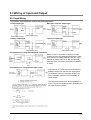
2.6 Clock/Calendar Function
If a backup battery is installed in the FP∑, the clock/calendar function can be used. This function cannot
be used without a backup battery.
2.6.1 Area for Clock/Calendar Function
With the clock/calendar function, data indicating the hour, minute, second, day, year and other
information stored in the special data registers DT90053 to DT90057 can be read using the transmission
instruction and used in sequence programs.
Special data
Upper byte
Lower byte
Reading
Writing
Register No.
Hour data
Minute data
DT90053
Available
Not available
H00 to H23
H00 to H59
Minute data
Second data
Available
Available
DT90054
H00 to H59
H00 to H59
Day data
Hour data
DT90055
Available
Available
H01 to H31
H00 to H23
Year data
Month data
Available
Available
DT90056
H00 to H99
H01 to H12
Day-of-the-week data
DT90057
Available
Available
H00 to H06
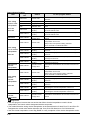
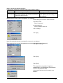
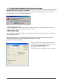
2.6.2 Setting of Clock/Calendar Function
There are two ways to set the clock/calendar function, as described below.
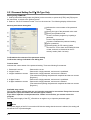
Setting using FPWIN GR
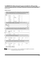
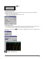
1. Press the [CTRL] and [F2] keys at the same time, to switch to the [Online] screen.
2. Select “Set PLC Date and Time” under “Tool” on the menu bar.
Set PLC Date and Time dialog box
The above steps display the “Set PLC Date and Time
dialog box” shown at the left. Input the date and time, and
click on the “OK” button.
Setting and changing using program
1. The values written to the special data registers DT90054 to DT90057, which are allocated as the
clock/calender setting area, are sent.
2. A value of H8000 is written to DT90058.
Note) The value can be sent using the differential instruction “DF”, or by changing H8000 to H0000.
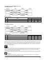
2-17
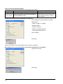
Example showing the date and time being written
Set the time to 12:00:00 on the 5th day when the X0 turns on.
Note:
No values have been set in the default settings, so the programming tool or another means must be
used to specify the values.
As a day of the week is not automatically set on FPWIN GR, fix what day is set to 00, and set
each value for 00 to 06.
2.6.3 Example Showing the Clock/Calendar being Used
Sample program for fixed schedule and automatic start
In the example shown here, the clock/calendar function is used to output the (Y0) signal for one second,
at 8:30 a.m. every day.
Here, the “Hour/minute” data stored in the special data register DT90053 is used to output the signal at
the appointed time.
The hour data is stored in the upper 8 bits of DT90053 and the minute data in the lower 8 bits, in the
BCD format. This hour and minute data is compared with the appointed time (BCD), and the R900B
(=flag) special internal relay is used to detect whether or not it matches the appointed time.
2-18
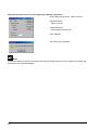
2.6.4 30-second Compensation Sample Program
This is a program to perform the compensation for 30 seconds when R0 is turned ON. If the 30-second
compensation is required, use this program.
2-19
2-20
Chapter 3
Expansion
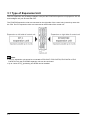
3.1 Type of Expansion Unit
The FPΣ expansion unit (including intelligent units) and the FP0/FP0R expansion unit (expansion I/O unit
and intelligent unit) can be used with FPΣ.
The FP0/FP0R expansion units are connected on the right side of the control unit, just as they were with
the FP0. The FPΣ expansion units are connected to the left side of the control unit.
Note:
• The FPΣ expansion unit cannot be connected to FPG-C32T, FPG-C32TTM, FPG-C32TH or FPGC32THTM. Only the FP0/FP0R expansion unit can be connected.
• Up to 2 units of FP∑ positioning unit RTEX can be installed.
3-2
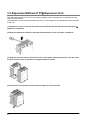
3.2 Expansion Method of FP0/FP0R Expansion Unit
The FP0/FP0R expansion unit (expansion I/O unit, intelligent unit) is expected by connecting to the right
side of the control unit.
Unit expansion is done using the right-side connector for FP0 expansion and expansion hook on the side
of the unit.
(1) Peel the seal on the side of the unit so that the internal right-side connector for FP0 expansion
is exposed.
(2) Raise the expansion hooks on the top and bottom sides of the unit with a screwdriver.
(3) Align the pins and holes in the four corners of the control unit and expansion unit, and insert
the pins into the holes so that there is no gap between the units.
(4) Press down the expansion hooks raised in step 2 to secure the unit.
3-3
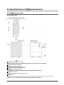
3.3 Expansion Method of FPΣ Expansion Unit
The dedicated expansion unit for FPΣ (including intelligent unit) is expanded by connecting to the left
side of the control unit.
Unit expansion is done using the left-side connector for FPΣ expansion and expansion hook on the side
of the unit.
(1) Remove the cover on the left side of the unit so that the internal left-side connector for FPΣ
expansion is exposed.
(2) Raise the expansion hooks on the top and bottom sides of the unit with a screwdriver.
(3) Align the pins and holes in the four corners of the control unit and expansion unit, and insert
the pins into the holes so that there is no gap between the units.
(4) Press down the expansion hooks raised in step 2 to secure the unit.
3-4
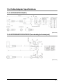
3.4 Specifications of FPΣ Expansion Unit
3.4.1 FPΣ Expansion Unit
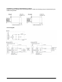
Parts and functions
① LED display selection switch
Switches between the input (32 points) and output (32 points) of the LED display.
② Input connector (40 pins)
③ Output connector (40 pins)
④ Input and Output indicator LEDs
⑤ FPΣ expansion connector
This expansion connector is used to connect the dedicated unit for FPΣ.
⑥ Expansion hook
This hook is used to secure expansion unit.
⑦ DIN hook
This lever enables the expansion unit to attach to a DIN rail at a touch. The lever is also used for
installation on the mounting plate (slim 30 type) (Product No.:AFP0811).
3-5
Input specifications
Item
Insulation method
Rated input voltage
Operating voltage range
Rated input current
Input points per common
Min. on voltage/Min. on current
Max. off voltage/Max. off current
Input impedance
off→on
Response time
on→off
Operating mode indicator
Description
Optical coupler
24 V DC
21.6 to 26.4 V DC
Approx. 3.5 mA
32 points/common
(Either the positive or negative of input power supply can be
connected to common terminal.)
19.2 V DC/3 mA
2.4 V DC/1.3 mA
Approx. 6.8 kΩ
0.2 ms or less
0.3 ms or less
LED display
Transistor output specifications
Item
Insulation method
Output type
Rated load voltage
Operating load voltage range
Max. load current
Max. surge current
Output points per common
Off state leakage current
On state voltage drop
off→on
Response time
on→off
External power
Voltage
supply for driving
Current
internal circuit
Surge absorber
Operating mode indicator
Short circuit protection
3-6
Description
NPN
Optical coupler
Open collector
5 to 24 V DC
4.75 to 26.4 V DC
0.1 A
0.5 A
32 points/common
100 µ or less
0.5 V or less
0.2 ms or less
0.5 ms or less
PNP
24 V CD
21.6 to 26.4 V DC
21.6 to 26.4 V DC
15 mA or less
30 mA or less
Zener diode
LED display
Short circuit prevention, Thermal protection
Limitations on number of simultaneous on points
Keep the number of points which are simultaneously on within the following range as determined by the
ambient temperature.
Circuit diagram
3-7
Terminal layout diagram
Note: The numbers in the connector are for the first expansion.
3-8
3.4.2 FPΣ Expansion Data Memory Unit
Parts and Functions
① POWER LED (Green)
② BATT LED (Red)
Lights out: The voltage of the internal secondary battery is normal.
Lights on: The voltage of the internal secondary battery decreases.
Also, the memory backup switches are off.
③ Memory backup switches
The factory default setting is “OFF” so turn both SW1 and 2 “ON” when using the unit. If these switches
are turned off, the memory backup is not available as the memory is separated from the internal battery.
Turn them on when the unit is used.
④ Connector for FPΣ expansion
This connector is used to expand the unit for FPΣ.
⑤ Expansion hook
This hook is used to secure expansion units. The hook is also used for installation on flat type mounting
plate (AFP0804).
⑥ DIN hook
The unit enables attachment at a touch to a DIN rail. The lever is also used for installation on slim 30
type mounting plate (AFP0811).
3-9
General specifications
Item
Ambient temperature/humidity
Storage temperature/humidity
Vibration resistance
Shock resistance
Noise immunity
Operation condition
Weight
Performance specifications
Item
Memory
Battery life
Consumption current (5V)
No of occupied I/O points
Description
0 to +55 °C, 30 to 85 %RH (at 25°C, non-condensing)
-20 to +70 °C, 30 to 85 %RH (at 25°C, non-condensing)
10 to 55 Hz, 1 cycle/min, double amplitude of 0.75 mm,
10 min on 3 axes
2
Shock of 98 m/s , 4 times on 3 axes
1000 Vp-p with pulse widths 50 ns and 1µs
(based on in-house measurements
Free from corrosive gases and excessive dust
Approx. 80 g
Description
256 k words (1k word x 256 banks)
5 years or more
100 mA or less
Input 16 points
Data organization
This unit is organized with 256 banks (1 k word = 1 bank).
Banks are assigned with numbers which are from “0” to “FF” in hexadecimal.
Each bank is assigned with an address for every word, and one bank is organized with 1024 words (1k
word) of a range within 0 to 3FF (0 to 1023 for decimal address).
Specify the above bank No. H0 to HFF (hexadecimal) and address (K0 to K1023) for reading data from
the control unit to this unit.
3-10
How to access the memory unit
The following instructions are used to access the expansion data memory unit to the control unit.
1. To read data from the expansion data memory unit to the control unit
S1: The area for specifying the slot No. of an Intelligent I/O unit (this unit) and bank numbers
Specify them in hexadecimal.
Higher byte
Bank No. H0 to HFF
Lower byte
Slot No. H0 to H3
S2: The first address (word address), K0 to K1023 (H0 to H3FF), for reading the memory of an
intelligent I/O unit (this unit)
The area for specifying addresses in the bank specified in S1
n: No. of words to read, K1 to K1024 (H1 to H400)
D: The first area No. to store read data
[Example]
When R0 is on, 10 words will be read from the address K500 of the bank No. H50 in the expansion
data memory unit installed in the slot No. 03 to store DT100 to DT109 in order.
2. To write data to the expansion data memory unit from the control unit
S1: The area for specifying the slot No. of an Intelligent I/O unit (this unit) and bank numbers
Specify them in hexadecimal.
Higher byte
Bank No. H0 to HFF
Lower byte
Slot No. H0 to H3
S2: The first area No. of write data
n: No. of words to write, K1 to K1024 (H1 to H400)
D: The first area No. to store write data
[Example]
When R0 is on, the contents of DT10, 11, 12 and higher are written for 10 words in order in the area
starting with the address H2FE of the bank No. HAB in the expansion data memory unit installed in
the slot No. H01.
3-11
Note:
• The operating time for the instructions is as follows.
F150 READ : 16.19+(0.84 x No. of words to read) µs
F151 WRITE : 17.88+(0.77 x No. of words to write) µs
• If all areas are read and written in one scan, the scanning time may be over.
• If you try to READ/WRITE data in multiple addresses in one scan, arrange the instructions using the
above operating time as a guide.
Battery error
When any error occurs in a backup battery, the input will be turned on as follows.
[Example] When installing in the expansion unit 1 (slot No. 0)
OFF
X100
ON
Lights out
BATT LED (Red)
Lights
Battery voltage is normal.
The battery voltage for memory backup decreased.
Or the memory backup SW is off.
Battery voltage is normal.
The battery voltage for memory backup decreased.
Or the memory backup SW is off.
Note:
• If an error with a battery is detected, backup the data within one month and replace the unit with a new
one.
3-12
Chapter 4
I/O Allocation
4.1 I/O Allocation
Regarding I/O number
• Specifying X and Y numbers
On the FPΣ and the FP0, the same numbers are used for input and output.
• Expression of numbers for input/output relays
Since input relay “X” and output relay “Y” are handled in units of 16 points, they are expressed as a
combination of decimal and hexadecimal numbers as shown below.
• Slot No.
Slot No. is the number indicating the installing position of the expansion unit which is used to generate
programs by some FPΣ expansion unit.
4-2
4.2 Allocation of FPΣ Control Unit
4.2.1 I/O Number of FPΣ Control Unit
The I/O allocation of FPΣ control unit is fixed.
Type of control unit
Number of allocation
FPG-C32T/FPG-C32TTM
Input (16 points)
FPG-C32T2/FPG-C32T2TM
Output (16 points)
FPG-C32TH/FPG-C32THTM
FPG-C28P2/FPG-C28P2TM
FPG-C28P2H/FPG-C28P2HTM
FPG-C24R2/FPG-C24R2TM
FPG-C24R2H/FPG-C24R2HTM
Input (16 points)
Output (16 points)
Input (16 points)
Output (8 points)
I/O number
X0 to XF
Y0 to YF
X0 to XF
Y0 to YB
X0 to XF
Y0 to Y7
4-3
4.3 Allocation of FPΣ Expansion Unit
The FPΣ expansion unit is installed on the left side of the FPΣ control unit.
The I/O numbers of the FPΣ expansion unit start with the lowest number at the right and proceed in
sequential order.
4.3.1 I/O Numbers of FPΣ Expansion Unit
• I/O do not need to be set as I/O allocation is performed automatically when an expansion unit is added.
• The I/O allocation of expansion unit is determined by the installation location.
Number of
allocation
Type of unit
FPΣ
Expansion
unit
FPGXY64D2T
1-axis type
FPG-PP11
FPG-PP12
FPΣ
Positioning
unit
FPΣ
Expansion
data
memory
unit
FPΣ
S-LINK unit
FPΣ
Positioning
unit RTEX
Note)
2-axis type
FPG-PP21
FPG-PP22
FPG-EM1
Input
32 points
Output
32 points
Input
16 points
Output
16 points
Input
32 points
Output
32 points
Input
16 points
-
1st axis
1st axis
2nd axis
1st axis
2nd axis
Battery
error
Expansion
Expansion
Expansion
unit 1
unit 2
unit 3
unit 4
Slot 0
Slot 1
Slot 2
Slot 3
X100 to
X11F
Y100 to
Y11F
X100 to
X10F
Y100 to
Y10F
X100 to
X10F
X110 to
X11F
Y100 to
Y10F
Y110 to
Y11F
X180 to
X19F
Y180 to
Y19F
X180 to
X18F
Y180 to
Y18F
X180 to
X18F
X190 to
X19F
Y180 to
Y18F
Y190 to
Y19F
X260 to
X27F
Y260 to
Y27F
X260 to
X26F
Y260 to
Y26F
X260 to
X26F
X270 to
X27F
Y260 to
Y26F
Y270 to
Y27F
X340 to
X35F
Y340 to
Y35F
X340 to
X34F
Y340 to
Y34F
X340 to
X34F
X350 to
X35F
Y340 to
Y34F
Y350 to
Y35F
X100 to
X10F
X180 to
X18F
X260 to
X26F
X340 to
X34F
X100 to
X17F
Y100 to
Y17F
X180 to
X25F
Y180 to
Y25F
X260 to
X33F
Y260 to
Y33F
X340 to
X41F
Y340 to
Y41F
Input
-
Output
-
Input
128 points
-
X100 to
X17F
X180 to
X25F
X260 to
X33F
X340 to
X41F
Output
128 points
-
Y100 to
Y17F
Y180 to
Y25F
Y260 to
Y33F
Y340 to
Y41F
FPG-SL
FPG-PN2AN
2-axis type
FPG-PN4AN
4-axis type
FPG-PN8AN
8-axis type
Expansion
• Regarding FPΣ CC-Link slave unit, please refer to the exclusive manual.
Note) There is no restriction on installed positions, however, the number of installed units is up to 2 units.
4-4
4.4 Allocation of FP0/FP0R Expansion Unit
The FP0/FP0R expansion unit is installed on the right side of the FPΣ control unit.
The I/O numbers start with the lowest number at the expansion unit nearest the control unit and proceed
in sequential order.
4.4.1 I/O Numbers of FP0/FP0R Expansion Unit
• I/O do not need to be set as I/O allocation is performed automatically when an expansion unit is added.
• The I/O allocation of expansion unit is determined by the installation location.
Number of
Expansion
Expansion
Expansion
Type of unit
allocation
unit 1
unit 2
unit 3
E8X
Input (8 points)
X20 to X27
X40 to X47
X60 to X67
Input (4 points)
X20 to X23
X40 to X43
X60 to X63
E8R
Output (4 points)
Y20 to Y23
Y40 to Y43
Y60 to Y63
E8TY/P
Output (8 points)
Y20 to Y27
Y40 to Y47
Y60 to Y67
E8YR
FP0/FP0R
E16X
Input (16 points)
X20 to X2F
X40 to X4F
X60 to X6F
Expansion
unit
Input (8 points)
X20 to X27
X40 to X47
X60 to X67
E16R
E16T/P
Output (8 points)
Y20 to Y27
Y40 to Y47
Y60 to Y67
E16YT/P
Output (16 points)
Y20 to Y2F
Y40 to Y4F
Y60 to Y6F
Input (16 points)
X20 to X2F
X40 to X4F
Y60 to Y6F
E32T/P
Output (16 points)
Y20 to Y2F
Y40 to Y4F
Y60 to Y6F
Input (16 points)
WX2
WX4
WX6
CH0
(X20 to X2F)
(X40 to X4F)
(X60 to X6F)
FP0
Input (16 points)
WX3
WX5
WX7
Analog
FP0-A21
CH1
(X30 to X3F)
(X50 to X5F)
(X70 to X7F)
I/O unit
WY2
WY4
WY6
Output (16 points)
(Y20 to Y2F)
(Y40 to Y4F)
(Y60 to Y6F)
FP0 A/D
Input (16 points)
WX2
WX4
WX6
conversion unit FP0-A80
CH0, 2, 4, 6
(X20 to X2F)
(X40 to X4F)
(X60 to X6F)
FP0
FP0-TC4
Input (16 points)
WX3
WX5
WX7
thermocouple
FP0-TC8
CH1, 3, 5, 7
(X30 to X3F)
(X50 to X5F)
(X70 to X7F)
unit
Input (16 points)
CH0, 2, 4
Input (16 points)
CH1, 3, 5
WX2
WX4
WX6
(X20 to X2F)
(X40 to X4F)
(X60 to X6F)
FP0
WX3
WX5
WX7
FP0-RTD6
RTD unit
(X30 to X3F)
(X50 to X5F)
(X70 to X7F)
WY2
WY4
WY6
Output (16 points)
(Y20 to Y2F)
(Y40 to Y4F)
(Y60 to Y6F)
WX2
WX4
WX6
Input (16 points)
(X20 to X2F)
(X40 to X4F)
(X60 to X6F)
FP0 D/A
Output (16 points)
WY2
WY4
WY6
FP0-A04V
conversion
CH0, 2
(Y20 to Y2F)
(Y40 to Y4F)
(Y60 to Y6F)
FP0-A04I
unit
Output (16 points)
WY3
WY5
WY7
CH1, 3
(Y30 to Y3F)
(Y50 to Y5F)
Y70 to Y7F)
Input 32 points
X20 to X3F
X40 to X5F
X60 to X7F
FP0
FP0-IOL
I/O link unit
Output 32 points
Y20 to Y3F
Y40 to Y5F
Y60 to Y7F
• The data for the each channels of FP0 A/D conversion unit (FP0-A80), FP0 thermocouple unit (FP0TC4/FP0-TC8), FP0 RTD unit(FP0-RTD6) and FP0 D/A conversion unit (FP0-A04V/FP0-A04I) is
converted and loaded with a user program that includes a switching flag to convert the data.
• Regarding FP0 CC-Link slave unit, please refer to the exclusive manual.
4-5
4-6
Chapter 5
Installation and Wiring
5.1 Installation
5.1.1 Installation Environment and Space
Operating environment
(Use the unit within the range of the general specifications when installing)
-Ambient temperatures:0 ~ +55 ℃
-Ambient humidity: 30% to 85% RH (at 25°C, non-condensing)
-Keep the height below 2000m.
-For use in pollution Degree 2 environment.
-Do not use it in the following environments.
- Direct sunlight
- Sudden temperature changes causing condensation.
- Inflammable or corrosive gas.
-Excessive airborne dust, metal particles or saline matter.
- Benzine, paint thinner, alcohol or other organic solvents or strong alkaline solutions such as ammonia
or caustic soda.
-Direct vibration, shock or direct drop of water.
- Influence from power transmission lines, high voltage equipment, power cables, power equipment,
radio transmitters, or any other equipment that would generate high switching surges.(100mm or
more)
Static electricity
- Do not touch connector pins directly to prevent static electricity from causing damage.
- Always rid yourself of any static electricity before handling this product.
Measures regarding heat discharge
• Always install the unit orientated with the tool port facing outward on the bottom in order to prevent the
generation of heat.
• Do not install the FPΣ control unit as shown below.
• Do not install the unit above devices which generate heat such heaters, transformers or large scale
resistors.
5-2
Installation space
• Leave at least 50mm/1.97 in. of space between the wiring ducts of the unit and other devices to allow
heat radiation and unit replacement.
• Maintain at least 100mm/3.937 in. of space between devices to avoid adverse affects from noise and
heat when installing a device or panel door to the front of the PLC unit.
• Leave at least 100mm/3.937 in. of space open from the front surface of the control unit in order to allow
room for programming tool connections and wiring.
5-3
5.1.2 Installation and Removal
Attachment to DIN rail and removal from DIN rail
FPΣ unit can be simply attached to DIN rail.
Procedure of installation method
(1) Fit the upper hook of the unit onto the DIN rail.
(2) Without moving the upper hook, press on the lower hook
to fit the unit into position.
Procedure of removal method
(1) Insert a slotted screwdriver into the DIN rail attachment
lever.
(2) Pull the attachment lever downwards.
(3) Lift up the unit and remove it from the rail.
5-4
5.1.3 Installation Using the Optional Mounting Plate
When using the slim 30 type mounting plate (AFP0811) (for mounting FPΣ)
Use M4 size pan-head screws for attachment of the slim 30 type mounting plate and install according to
the dimensions shown below.
The rest of the procedure is the same as that for attaching the unit to the DIN rails.
When using the slim type mounting plate (AFP0803) (for mounting FP0)
Use M4 size pan-head screws for attachment of the slim type mounting plate and install according to the
dimensions shown below.
The rest of the procedure is the same as that for attaching the unit to the DIN rails.
5-5
Note) The procedure for the removal is the same as AFP0811.
Note:
When using an expansion unit, tighten the screws after joining all of the slim type mounting plate to be
connected. Tighten the screws at each of the four corners.
[Example] When using the maximum numbers of the expansion units (with AFP0811, AFP0803)
5-6
When using the flat type mounting plate (AFP0804)
Use M4 size pan-head screws for attachment of the slim type mounting plate and install according to the
dimensions shown below.
Raise the expansion hooks on the top and bottom of the unit.
Align the expansion hooks with the mounting plate and press the hooks on the top and bottom.
An unit with an attached flat type mounting plate can also be installed sideways on a DIN rail.
Note:
The flat type mounting plate (AFP0804) should be used only with the control unit as a stand-alone unit. It
should not be used when the control unit is being used in combination with an FP0 expansion unit or
FPΣ expansion unit.
5-7
5.2 Wiring of Power Supply
5.2.1 Wiring of Power Supply
Power supply wiring for the unit
Use the power supply cable (Product No.:AFPG805) that comes with the unit to connect the power
supply.
Brown: 24V DC
Blue: 0V Green:
Function earth
Power supply wire
To minimize adverse effects from noise, twist the brown and blue wires of the power supply cable.
Power supply type
• To protect the system against erroneous voltage from the power supply line, use an insulated power
supply with an internal protective circuit.
• The regulator on the unit is a non-insulated type.
• If using a power supply device without an internal protective circuit, always make sure power is
supplied to the unit through a protective element such as a fuse.
Power supply voltage
Rated voltage
Operating voltage range
5-8
24V DC
21.6 to 26.4 V DC
Wiring system
Isolate the wiring systems to the control unit, input/output devices, and mechanical power apparatus.
Measures regarding power supply sequence (start up sequence)
• The power supply sequence should be set up so that power to the control unit is turned off before the
input/output power supplies.
• If the input/output power supplies are turned off before the power to the control unit, the control unit will
detect the input fluctuations and may begin an unscheduled operation.
• Be sure to supply power to a control unit and an expansion unit from the same power supply, and turn
the power on and off simultaneously for both.
5-9
5.2.2 Grounding
In situations of excess noise
Under normal conditions, the inherent noise resistance is sufficient. However, in situations of excess
noise, ground the instrument to increase noise suppression.
Exclusive grounding
• The grounding connection should have a resistance of less than 100Ω.
• The point of grounding should be as close to the PLC unit as possible. The ground wire should be as
short as possible.
• If two devices share a single ground point, it may produce an adverse effect. Always use an exclusive
ground for each device.
Note:
Depending on the surroundings in which the equipment is used, grounding may cause problems.
[Example]
Since the power supply line of the FPΣ power supply connector is connected to the function earth
through a varistor, if there is an irregular potential between the power supply line and earth, the varistor
may be shorted.
Do not ground the FPΣ function earth terminal when grounding a plus (+) terminal of the power.
In some computers, the SG terminal of RS232C port and connector shielding are connected. Also the
FPΣ tool port shielding is connected with the function earth terminal. Therefore, the GND terminal of FPΣ
and the function earth terminal are connected if the computer is connected. Especially when the FPΣ is
connected to a computer with a plus (+) terminal grounded, therefore, an FPΣ’s minus (-) terminal is
connected with the function earth terminal. As a result, short circuit occurs which may lead to the
breakage of FPΣ and its neighboring parts.
5-10
5.3 Wiring of Input and Output
5.3.1 Input Wiring
Connection of photoelectric sensor and proximity sensor
Relay output type
NPN open collector output type
Voltage output type
Two-wire output type
Precaution when using LED-equipped reed switch
When a LED is connected in series to an input
contact such as LED-equipped reed switch, make
sure that the on voltage applied to the PLC input
terminal is greater than 21.6V DC. In particular,
take care when connecting a number of switches
in series.
Precaution when using two-wire type sensor
If the input of PLC does not turn off because of
leakage current from the two-wire type sensor
“photoelectric sensor or proximity sensor”, the
use of a bleeder resistor is recommended, as
shown below.
The formula is based on an input impedance of
5.6kΩ. The input impedance varies depending on
the input terminal number.
5-11
Precaution when using LED-equipped limit switch
If the input of PLC does not turn off because of the
leakage current from the LED-equipped limit
switch, the use of a bleeder resistor is
recommended, as shown below.
5-12
5.3.2 Output Wiring
Protective circuit for inductive loads
• With an inductive load, a protective circuit should be installed in parallel with the load.
• When switching DC inductive loads with relay output type, be sure to connect a diode across the ends
of the load.
When using an AC inductive load
When using a DC inductive load
Precautions when using capacitive loads
When connecting loads with large in-rush currents, to minimize their effect, connect a protection circuit
as shown below.
About the short-circuit protective circuit
To prevent the output circuit from being damaged by a short-circuit or other electrical problems on the
output side, a transistor with short-circuit protection is provided.
(Excluding the Y0, 1, 3, 4 of the FPΣ control unit and the FP0 expansion unit)
5-13
5.3.3 Precautions Regarding Input and Output Wirings
• Be sure to select the thickness (dia.) of the input and output wires while taking into consideration the
required current capacity.
• Arrange the wiring so that the input and output wiring are separated, and these wirings are separated
from the power wiring, as much as possible. Do not route them through the same duct or wrap them up
together.
• Separate the input/output wires from the power and high voltage wires by at least 100mm/3.937 in.
5-14
5.4 Wiring of MIL Connector Type
Supplied connector and suitable wires
The connector listed below is supplied with the FPΣ control unit. Use the suitable wires given below. Also,
use the required pressure connection tools for connecting the wires.
Suitable wires
Nominal crossInsulation
Rated
Remark
sectional area
thickness
current
2
AWG#22
0.3mm
Twisted wire of 12 pcs/0.18
Dia. 1.5 to dia. 1.1
3A
2
AWG#24
0.2mm
Twisted wire
Note) The contact suitable for AWG#22 or AWG#24 is supplied with the product. For purchasing a
contact suitable for AWG#26 or AWG#28, specify AFP7231FP.
Size
Supplied connector (Attached to FPΣ control unit)
Manufacturer
Component parts
Required quantity
Housing(10P)
2 pcs x 2sets
Manufactured by us
Semi-cover(10P)
4 pcs x 2sets
Contact(for AW22 and 24)5 pins 4 pcs x 2sets
Note) The parts of the number of the connectors are supplied with the product. If you need more
connectors, purchase AFP0807 (2 sets/pack).
Supplied connector (Attached to FPΣ expansion unit)
Manufacturer
Component parts
Required quantity
Housing(40P)
1 pc x 2sets
Manufactured by us
Semi-cover(40P)
2 pcs x 2sets
Contact(for AW22 and 24)5 pins 8 pcs x 2sets
Note) The parts of the number of the connectors are supplied with the product. If you need more
connectors, purchase AFP2801 (2 sets/pack).
Pressure connection tool
Manufacturer
Manufactured by us
Product No.
AXY52000FP
Key Point:
When using a MIL connector for flat cables, purchase the product number AFP0808 (4 pcs,
10-pin strain-relief with key). In this case, the suitable wire is AWG#28 and the rated current is
1A.
5-15
Procedure of assembly (Wiring method)
The wire end can be directly crimped without removing the wire’s insulation, saving labor.
(1) Bend the welder (contact) back from the carrier, and set it in the pressure connection tool.
(2) Insert the wire without removing its insulation until it stops, and lightly grip the tool.
(3) After press-fitting the wire, insert it into the housing.
(4) When all wires has been inserted, fit the semi-cover into place.
If there is a wiring mistake or the cable is incorrectly pressure-connected, the contact puller pin provided
with the fitting can be used to remove the contact.
Key Point:
If using a MIL connector for flat cables, specify the product No. AXM110915.
In this case, the suitable wire is AWG#28 and the rated current is 1A.
5-16
5.5 Wiring of Terminal Block Type
A screw-down connection type for terminal block is used. The suitable wires are given below.
Terminal block socket
Item
Number of pin
Manufacturer
Model No.
Product No.
Suitable wires
Size
AWG #24 to 16
Description
9 pins
Phoenix Contact Co.
MC1,5/9-ST-3,5
1840434
Nominal cross-sectional area
2
0.2 to 1.25mm
Pole terminal
If a pole terminal is being used, the following models manufactured by Phoenix Contact Co. should be
used.
Manufacturer
Cross-sectional Size
Part No.
2
area (mm )
With insulating
Without insulating
sleeve
sleeve
0.25
AWG #24
AI 0,25 – 6 BU
A 0,25 – 7
0.34
AWG #22
AI 0.34 – 6 TQ
A 0,34 – 7
0.50
AWG #20
AI 0,5 – 6 WH
A 0,5 – 6
Phoenix
0.75
AWG #18
AI 0,75 – 6 GY
A 0,75 – 6
Contact Co.
1.00
AWG #18
–
A 1 – 60
0.5×2
AWG #20 (for 2
AI – TWIN 2×
–
pcs)
0.5 – 8 WH
Pressure welding tool for pole terminals
Manufacturer
Part No.
Phoenix Contact Co. CRIMPFOX 6
Product No.
1212034
For tightening the terminal block
When tightening the terminals of the terminal block, use a screwdriver (Product No. 1205037) with a
blade size of 0.4 × 2.5 (Part No. SZS 0,4×2,5).
The tightening torque should be 0.22 to 0.25 N・m (2.3 to 2.5 kgf・cm) or less.
5-17
Wiring method
(1) Remove a portion of the wire’s insulation.
(2) Insert the wire into the terminal block until it contacts the back of the block socket, and then
tighten the screw clockwise to fix the wire in place. (Tightening torque: 0.22 N·m to 0.25 N·m
(2.3 kgf·cm to 2.5 kgf·cm))
Note:
• When removing the wire’s insulation, be careful not to scratch the core wire.
• Do not twist the wires to connect them.
• Do not solder the wires to connect them. The solder may break due to vibration.
• After wiring, make sure stress is not applied to the wire.
• In the terminal block socket construction, if the wire closes upon counter-clockwise rotation, the
connection is faulty. Disconnect the wire, check the terminal hole, and then re-connect the wire.
5-18
5.6 Safety Measures
5.6.1 Safety Measures
Precautions regarding system design
In certain applications, malfunction may occur for the following reasons:
• Power on timing differences between the PLC system and input/output or mechanical power apparatus.
• Response time lag when a momentary power drop occurs.
• Abnormality in the PLC unit, external power supply, or other devices.
In order to prevent a malfunction resulting in system shutdown choose the adequate safety measures
listed in the following:
Interlock circuit
When a motor clockwise/counter-clockwise operation is controlled, provide an interlock circuit externally.
Emergency stop circuit
Provide an emergency stop circuit to the PLC externally to turn off the power supply of the output device.
Start up sequence
The PLC should be operated after all of the outside devices are energized. To keep this sequence, the
following measures are recommended:
• Turn on the PLC with the mode selector set to the PROG. mode, and then switch to the RUN mode.
• Program the PLC so as to disregard the inputs and outputs until the outside devices are energized.
Note) In case of stopping the operation of the PLC also, have the input/output devices turned off after
the PLC has stopped operating.
Grounding
When installing the PLC next to devices that generate high voltages from switching, such as inverters,
do not ground them together. Use an exclusive ground for each device.
5.6.2 Momentary Power Failures
Operation of momentary power failures
If the duration of the power failure is less than 3 ms, the FPΣ continues to operate. If the power is off for
3 ms or longer, operation changes depending on the combination of units, the power supply voltage, and
other factors. (In some cases, operation may be the same as that for a power supply reset.)
5-19
5.6.3 Protection of Power Supply and Output Sections
Power supply
An insulated power supply with an internal protective circuit should be used. The power supply for the
control unit operation is a non-insulated circuit, so if an incorrect voltage is directly applied, the internal
circuit may be damaged or destroyed. If using a power supply without a protective circuit, power should
be supplied through a protective element such as a fuse.
Protection of output
If current exceeding the rated control capacity is being supplied in the form of a motor lock current or a
coil shorting in an electromagnetic device, a protective element such as a fuse should be attached
externally.
5-20
5.7 Handling of Backup Battery
5.7.1 What Backup Battery Does
Install an optional backup battery when the hold area is insufficient in the initial state or for using the
clock/calender function.
Areas backed up with the battery
Classification
Timer and counter
Timer and counter
Elapsed value area
Operation
memory
Special data
register
Hold area when battery
is not installed
C1008 - C1023
EV1008 - EV1023
Data register
Step ladder
Link relay
Link register
12k type: R900 – R97F
32k type: R2480-R255F
DT32710 – DT32764
None
None
None
Clock/calender
None
Internal relay
Hold area when battery
is installed
Hold areas or non-hold areas
can be specified arbitrarily by
setting the system registers
No.6 to No.13 using a
programming tool. (All points
can be also held.)
All points
Type of backup batteries (Sold separately)
Appearance
Product name
Specifications
Product No.
Backup battery
for FPΣ
With a connector
AFPG804
High-capacity
battery folder
for FPΣ
Battery folder with a connector
Purchase a commercial battery
CR123A separately.
AFPG807
(Folder only)
5-21
5.7.2 Settings of Battery Error Alarm and Hold Area
Setting of the battery error alarm
- Setting the battery error alarm enables you to monitor the remaining backup battery level. By default,
the battery error alarm is set to off in the system register settings. For using the battery, check the box
of the system register No.4 "Alarm Battery Error" of the control unit.
Settings of Hold area/Non-hold area
- The settings of the operation memory area such as data registers and system registers No.6 to No.14
are necessary.
Note:
- When "Battery Error Alarm" is not set, the ERR.LED will not flash even if a battery error is detected.
Note that data may be lost as the result of the battery shutoff.
- The setting of the system registers Nos. 6 to 14 are effective only when the backup battery is installed.
- Without the battery, use at the default settings. If changing the settings, the “Hold/Non-hold” operation
becomes unstable.
5-22
5.7.3 Replacement of Backup Battery
The procedure for replacing the backup battery is as follows.
Procedure
1. Supply power to the control unit for more than one minute.
Charge the built-in capacitor to retain the contents of the memory during the replacement of the battery.
1. Turn off the power supply.
Remove the battery cover using a tool such as a screwdriver.
4. Remove the used battery.
5. Install a new battery within two minutes after turning off the power of the control unit.
Connect the connector, and place the battery between two tabs.
6. Install the expansion cover.
Note:
- If the power is not sufficiently supplied or it takes too much time to replace the battery, retained memory
data may be lost.
5-23
Replacement procedure (for high-capacity battery folder for FP AFPG807 and commercial
battery CR123A)
1. Supply power to the control unit for more than one minute.
Charge the built-in capacitor to retain the contents of the memory during the replacement of the battery.
2. Turn off the power.
3. Remove the used battery.
4. Install a new battery within two minutes after turning off the power of the control unit.
Note:
- If the power is not sufficiently supplied or it takes too much time to replace the battery, retained memory
data may be lost.
Precaution when using FP high-capacity battery folder AFPG807
- Do not touch the terminals of the folder and connector pins directly to prevent electrostatic discharge
failure. Always rid yourself of any static electricity before handling this product. Make sure that the parts
such as the lead wires and connector parts are not stressed when and after installing it.
- Use M3-flat head screws or a double-faced tape for mounting the folder.
- The connector to connect with the FP does not have a lock mechanism. Fix the lead wire to prevent
the connector from dropping off.
(Installation illustration)
- Install the battery cover pulling out a lead wire through the gap between the control unit and the battery
cover.
Installed state of battery cover
25.4
43.9
(Dimensions of battery folder AFG807)
16.5
20.5
5-24
100
±20
5.7.4 Lifetime and Time for Replacement of Backup Battery
Battery lifetime
Type of backup battery
Battery lifetime
Suggested
replacement interval
When using a backup battery for FPΣ (AFPG804)
220 days or more
1 year
6 years or more
6 years
When using a commercial battery CR123A and
FPΣ high-capacity battery folder (AFPG807)
Note1) The battery lifetime is the value when no power at all is supplied.
Note2) Note that the lifetime in actual use may be shorter than the typical lifetime depending on the use
conditions.
Note3) The battery is used for the battery detection circuit even when power is supplied. The lifetime is
about twice as long as that when no power is supplied.
Detection of battery error and time for replacement
- Special internal relays R9005 and R9006 will go on if the battery voltage drops. Create a program to
announce errors to the outside as necessary. Two seconds after starting supplying power, the battery
voltage is checked. Therefore, an error is not announced in the first scan.
- When the system register No.4 "Battery Error Alarm" is enabled, the ERR.LED of the control unit will
flash.
- Although data will be retained for about a week after the detection of battery error without power, the
battery should be replaced as soon as possible.
Note:
- if a week has passed without power after the special internal relays R9005 and R9006 turned on or the
ERR.LED flashed, retained memory data may be lost.
- Regardless of how much time has passed after the detection of battery error, supply power to the
control unit for more than one minute when replacing the battery.
- Special internal relays R9005 and R9006 will be on when a battery error is detected regardless of the
setting of system register No.4.
5-25
5-26
Chapter 6
High-speed counter, Pulse Output and
PWM Output functions
6.1 Overview of Each Functions
6.1.1 Three Functions that Use Built-in High-speed Counter
There are three functions available when using the high-speed counter built into the FPΣ.
High-speed counter function
The high-speed counter function counts external
inputs such as those from sensors or encoders.
When the count reaches the target value, this
function turns on/off the desired output.
Pulse output function
Combined with a commercially available motor
driver, the function enables positioning control.
With the exclusive instruction, you can perform
trapezoidal control, home return, and JOG
operation.
PWM output function
By using the exclusive instruction, the PWM output
function enables a pulse output of the desired duty
ratio.
6-2
6.1.2 Performance of Built-in High-speed Counter
Number of Channel
• There are four channels for the built-in high-speed counter
• The channel number allocated for the high-speed counter will change depending on the function being
used.
Counting range
• K-2, 147, 483, 648 to K+2, 147, 483, 647 (Coded 32-bit binary)
• The built-in high-speed counter is a ring counter. Consequently, if the counted value exceeds the
maximum value, it returns to the minimum value. Similarly, if the counted value drops below the
minimum value, it goes back to the maximum value and continues counting from there.
Note:
When the linear interpolation instruction F175 or the circular interpolation instruction F176 is used, the
value for the target value or the amount of travel should be set so that it is within the range indicated
below.
-8,388,608 to +8,388,607 (Coded 24-bit binary)
The F175 and F176 instructions can be used only with the C32T2, C28P2, C32T2H and C28P2H control
units.
6-3
6.2 Function Specifications and Restricted Items
6.2.1 Specifications
High-speed counter function
High-speed counter
channel No.
CH0
[Single phase]
Incremental,
Decremental
[2-phase]
2-phase input
One input,
Direction
distinction
Input/output
contact No.
being used
Input contact
number
(value in
parenthesis
is reset
input) Note1)
X0
(X2)
Memory area being used
Control
flag
R903A
DT90044
to
DT90045
Maximum counting
speed
DT90046
to
DT90047
DT90048
to
DT90049
DT90050
to
DT90051
R903C
DT90200
to
DT90201
DT90202
to
DT90203
X4
(X5)
R903D
DT90204
to
DT90205
DT90206
to
DT90207
X0
X1
(X2)
R903A
DT90044
to
DT90045
DT90046
to
DT90047
X3
X4
(X5)
R903C
DT90200
to
DT90201
DT90202
to
DT90203
R903B
CH2
X3
(X5)
CH3
CH0
CH2
Target
value area
Minimum
input
pulse
width
Note2)
X1
(X2)
CH1
Elapsed
value area
Performance specifications
10µs
(100µs)
Using 1 channel:
Max. 50kHz (x1-ch)
Using 2 channels:
Max. 30kHz (x2-ch)
Using 3 channels:
Max. 20kHz (x3-ch)
Using 4 channels:
Max. 20kHz (x4-ch)
25µs
(100µs)
Using 1 channel:
Max. 20kHz (x1-ch)
Using 2 channels:
Max. 15kHz (x2-ch)
Related instructions:
F0(MV) :High-speed counter control
F1(DMV) :Read/write of elapsed value of high-speed counter
F166(HC1S) :Target value match on (Specify the desired output from Y0 to Y7 using instruction)
F167(CH1R) :Target value match off (Specify the desired output from Y0 to Y7 using instruction)
Note1) Reset input X2 can be set to either CH0 or CH1. Reset input X5 can be set to either CH2 or CH3.
Note2) Reference: For information on minimum input pulse width,
see <6.3.3 Minimum Input Pulse Width>.
6-4
Pulse output function
High-speed
counter
channel No.
Input/output contact number used
DeviCCW
CW
ation
or
Near
or
coundireHome
home
pulse
ter
ction
input
input
outclear
Note4)
output
output
put
Memory area used
Control
flag
Elapsed
value
area
Target
value area
CH0
Y0
Y1
Y2
X2
DT9005
2
<bit4>
R903A
DT90044 to
DT90045
DT90046 to
DT90047
CH2
Y3
Y4
Y5
X5
DT9005
2
<bit4>
R903C
DT90020 to
DT90201
DT90202 to
DT90203
Linear
Y0
Y3
Y1
Y4
Y2
Y5
X2
X5
Note3)
Note3)
DT9005
2
<bit4>
R903A
R903C
DT90044 to
DT90045
DT90200 to
DT90201
DT90046 to
DT90047
DT90202 to
DT90203
Circular
Y0
Y3
Y1
Y4
Y2
Y5
X2
X5
Note3)
Note3)
DT9005
2
<bit4>
R903A
R903C
R904E
R904F
DT90044 to
DT90045
DT90200 to
DT90201
DT90046 to
DT90047
DT90202 to
DT90203
Independence
Interpolation
Max. output frequency
- Using one ch: Max. 100 kHz (x1-ch)
- Using two chs: Max. 60 kHz (x2-ch)
-Using linear interpolation: Max. 100 kHz
- Using circular interpolation: Max. 20 kHz
Related instructions
F0 (MV) :high-speed counter control
F1 (DMV) :Read/write of elapsed value of high-speed counter
F171 (SPDH) :trapezoidal control/home return
F172 (PLSH) :JOG operation
F174 (SP0H) :Data table control
F175 (SPSH) :Linear interpolation control
F176 (SPCH) :circular interpolation control
Note1) The pulse output function is only available with the transistor output type.
Note2) Linear and circular interpolation control is only available with the C32T2 or C28P2 units.
Note3) The home return operation of the interpolation axes should be performed for every channel.
Note4) Reference: For DT90052, see <6.4.4 Pulse Output Control Instruction (F0) (F1)>.
PWM output function
Highspeed
Output
counter
contact
channel
No. used
No.
Memory
area used
Control flag
Output frequency
(duty)
Related instructions
F0(MV) (High-speed
counter control)
F1(DMV) (Read/write of
elapsed value of highspeed counter)
CH2
Y3
R903C
F173(PWMH) (PWM
output)
Note) The PWM output function is only available with the transistor output type.
CH0
Y0
R903A
-When resolution = 1000,
1.5 Hz to 12.5 kHz
(0.0 to 99.9%)
-When resolution = 100,
15.6 kHz to 41.7 kHz
(0 to 99%)
6-5
6.2.2 Functions Used and Restrictions
Restrictions on channels/maximum counting speed (frequency)
The same channel cannot be used by more than one function. The maximum frequency when using the
high-speed counter and pulse output function is determined by the combination, as shown in the table
below.
A: Available
Max. counting speed
Channel being used
(frequency) [kHz]
High-speed
High-speed counter
Pulse output
Pulse output
counter
Single phase
2-phase
Independence
Inde- InterInterpo- Single
2penpolalation
phase phase
CH0 CH1 CH2 CH3 CH0 CH2
CH0
CH2
dence
tion
A
50
50
50
50
30
30
30
30
30
30
20
20
20
20
A
A
A
A
A
A
A
A
A
A
A
A
A
A
A
A
A
A
A
A
A
A
A
A
A
A
A
A
A
A
A
A
A
A
A
A
A
A
A
A
20
20
20
A
A
A
A
A
20
20
20
20
15
15
15
20
15
15
15
15
A
A
Note3)
A
Note3)
A
A
A
A
A
A
A
100
A
30
60
A
20
45
A
A
A
20
20
15
15
A
A
Note3)
A
A
A
Note3)
A
A
A
6-6
A
A
30
45
30
100
A
30
60
A
20
45
A
A
A
20
20
15
15
30
45
30
Channel being used
High-speed counter
Single phase
CH0
CH1
CH2
Pulse output
2-phase
CH3
A
Note3)
A
Note3)
A
A
Note3)
Note3)
A
Note3)
A
Note3)
A
A
Note3)
Note3)
CH0
CH2
Independence
CH0
CH2
Interpolation
A: Available
Max. counting speed
(frequency) [kHz]
High-speed
Pulse output
counter
Inde- InterSingle
2penpolaphase phase
dence
tion
A
A
Note1)
Note1)
A
A
20
45
A
A
20
45
A
A
20
30
60
100
Linear
Note2)
Linear
80
Linear
20
60
Linear
20
60
Linear
20
45
Circular
A
Note3)
A
Note3)
A
A
Note3)
Note3)
20
Circular
20
20
Circular
20
20
Circular
20
20
Note1)If two channels are not executed simultaneously, each axis may be used up to 100 kHz.
Note2)These are the values when PC link and fixed-interval interrupt function are not used.
Note3)When using CH0 pulse output, do not use the hard reset (X2) at CH0 and CH1 of HSC.
When using CH2 pulse output, do not use the hard reset (X5) at CH2 and CH3 of HSC.
Restrictions on I/O allocations
• The inputs and outputs allocated to the various functions listed in the table in the previous section
“6.2.1” cannot be allocated to more than one function.
• Except for the examples noted below, inputs and outputs that have been allocated to the various
functions cannot be allocated as normal inputs and outputs.
Example 1:
If no reset input is used in the high-speed counter function, X2 and X5 can be as normal inputs.
Example 2:
If no output is used to clear the differential counter in the pulse output function, Y2 and Y5 can be used
as normal outputs.
Restrictions on the execution of related instructions (F166 to F176)
• If an instruction related to the high-speed counter “F166 to F176” is executed, the control flag (special
internal relay: R903A to R903D) corresponding to the channel used turns on.
6-7
• Please be aware that the control flag “in progress” may change while a scan is being carried out. To
prevent multiple read access to this special internal relay, you should generate a copy of it at the
beginning of the program.
• When the control flag for a channel turns on, another instruction using that same channel cannot be
executed.
• Executing circular interpolation control instruction F176 sets the circular interpolation in progress flag
(special internal relay: R904E), and that state is maintained until the target value is achieved. During
this time, other pulse output instructions (F171 to F176) cannot be executed.
6-8
6.2.3 Booting Time
The booting time is the time span from the execution of the instruction to the actual pulse output.
Type of instruction
Booting time
CW/CCW is set :
Approx. 200 µs (with 30 steps)
Pulse output instruction F171
Approx. 400 µs (with 60 steps)
(SPDH)
Note)
Pulse/direction is set :
Approx. 500 µs (with 30 steps)
Trapezoidal control/home return
Note)
Approx. 700 µs (with 60 steps)
Pulse output instruction F172
CW/CCW is set :
Approx. 20 µs
(PLSH)
Note)
Pulse/direction is set :
Approx. 320 µs
JOG operation
Pulse output instruction F174
CW/CCW is set :
Approx. 30 µs
(SP0H)
Note)
Pulse/direction is set :
Approx. 330 µs
Data table control
PWM output instruction F173
Approx. 30 µs
(PWMH)
Note) If pulse/direction is set, a waiting time (approx. 300 µs) is included from the time that the direction
output goes on until the pulse output instruction can be executed.
6-9
6.3 High-speed Counter Function
6.3.1 Overview of High-speed Counter Function
• The high-speed counter function counts the input signals, and when the count reaches the target value,
turns on and off the desired output.
• To turn on an output when the target value is matched, use the target value match ON instruction F166
(HC1S). To turn off an output, use the target value match OFF instruction F167 (HC1R).
• Preset the output to be turned on and off with the SET/RET instruction.
Setting the system register
In order to use the high-speed counter function, it is necessary to set system register numbers nos. 400
and 401.
6.3.2 Input Modes and Count
Incremental input mode
Decremental input mode
Two-phase input mode
Incremental/decremental input mode
Direction discrimination
6-10
Count for reset input
(Incremental input mode)
The reset input is executed by the interruption at (1) on (edge)
and (2) off (edge).
(1) on (edge) … Count disable, Elapsed value clear
(2) off (edge) … Count enable
DT90052 (bit2): “able/disable” setting of the input can be set
by the reset input.
6.3.3 Minimum Input Pulse Width
For the period T (1/frequency), a minimum input pulse width of T/2 (single-phase input) or T/4 (twophase input) is required.
<Single phase>
<Two-phase>
6-11
6.3.4 I/O Allocation
• As shown in the table in the previous section “6.2.1”, the inputs and outputs used will differ depending
on the channel number being used.
• The output turned on and off can be specified from Y0 to Y7 as desired with instructions F166 (HC1S)
and F167 (HC1R).
When using CH0 with incremental input and
When using CH0 with two-phase input and
reset input
reset input
* The output turned on and off when the target
value is reached can be specified from Y0 to Y7
as desired.
* The output turned on and off when the target
value is reached can be specified from Y0 to Y7
as desired.
6.3.5 Instructions used with High-speed Counter Function
High-speed counter control instruction (F0)
• This instruction is used for counter operations such as software reset and count disable.
• Specify this instruction together with the special data register DT90052.
• Once this instruction is executed, the settings will remain until this instruction is executed again.
Operations that can be performed with this instruction
• Counter software reset (bit0)
• Counting operation enable/disable (bit1)
• Hardware reset enable/disable (bit2)
• Clear high-speed counter instructions F166 to F176
• Clear target value match interrupt
Example: Performing a software reset
In case of CH0
In the above program, the reset is performed in step
(1) and 0 is entered just after that in step (2). The
count is now ready for operation. If it is only reset,
counting will not be performed.
In case of CH1
6-12
High-speed counter/pulse output control flag area of FPΣ
• The area DT90052 for writing channels
and control codes is allocated as shown in
the left figure.
• Control codes written with an F0 (MV)
instruction are stored by channel in
special data registers DT90190 to
DT90193.
Note) In the reset input setting, the reset
input (X2 or X5) allocated in the high-speed
counter setting of the system registers are
defined to “enable/disable”.
6-13
Elapsed value write and read instruction (F1)
• This instruction changes or reads the elapsed value of the high-speed counter.
• Specify this instruction together with the special data register DT90044.
• The elapsed value is stored as 32-bit data in the combined area of special data registers DT90044 and
DT90045.
• Use this F1 (DMV) instruction to set the elapsed value.
Example 1: Writing the elapsed value
Set the initial value of K3000 in the high-speed
counter.
Example 2: Reading the elapsed value
Read the elapsed value of the high-speed
counter and copies it to DT100 and DT101.
Target value match ON instruction (F166)
Example 1:
If the elapsed value (DT90044 and DT90045)
for channel 0 matches K10000, output Y7 turns
on.
Example 2:
If the elapsed value (DT90200 and DT90201)
for channel 2 matches K20000, output Y6 turns
on.
Target value match OFF instruction (F167)
Example 1:
If the elapsed value (DT90048 and DT90049)
for channel 1 matches K30000, output Y4 turns
off.
Example 2:
If the elapsed value (DT90204 and DT90205)
for channel 3 matches K40000, output Y5 turns
off.
6-14
6.3.6 Sample program
Positioning operations with a single speed inverter
Wiring example
Operation chart
I/O allocation
I/O No.
Description
X0
Encoder input
X5
Operation start signal
Y0
Inverter operation signal
R100
Positioning operation running
R101
Positioning operation start
R102
Positioning done pulse
R903A
High-speed counter CH0 control flag
Program
When X5 is turned on, Y0 turns on and the conveyor begins moving. When the elapsed value (DT90044
and DT90045) reaches K5000, Y0 turns off and the conveyor stops.
6-15
Positioning operations with a double speed inverter
Wiring example
Operation chart
6-16
I/O allocation
I/O No.
Description
X0
Encoder input
X5
Operation start signal
Y0
Inverter operation signal
Y1
Inverter high-speed signal
R100
Positioning operation running
R101
Positioning operation start
R102
Arrival at deceleration point
R103
Positioning done pulse
R900C
Comparison instruction <flag>
R903A
High-speed counter CH0 control flag
Program
When X5 is turned on, Y0 and Y1 turn on and the conveyor begins moving. When the elapsed value
(DT90044 and DT90045) reaches K4500, Y1 turns off and the conveyor begins decelerating. When the
elapsed value reaches K5000, Y0 turns off and the conveyor stops.
6-17
6.4 Pulse Output Function
6.4.1 Overview of Pulse Output Function
Instructions used and controls
Together with a commercially available pulse-string input type motor driver, the pulse output function can
be used for positioning control.
Exclusive
Type of control
instruDescription
Usable unit
ction
Provides trapezoidal (table-shaped) control for
automatically obtaining pulse outputs by
Trapezoidal control
F171
specifying the initial speed, maximum speed,
(SPDH)
C32T
acceleration/deceleration time and target value.
C32T2
Home return
Enables automatic home return operation.
C28P2
Causes pulses to be output as long as the
C32TH
execution condition is on. A target value can
F172
C32T2H
JOG operation
also be set, so that pulse output stops at the
(PLSH)
C28P2H
point when the target value is matched.
F174
Enables positioning control in accordance with
Data table control
(SP0H)
the data table.
Enables pulses to be output using linear
interpolation control, by specifying the
F175
Linear interpolation
composite speed, the acceleration/deceleration
(SPSH)
C32T2
time, and the target value.
C28P2
The user can select one of two circular forming
C32T2H
methods, one by specifying the pass positions
C28P2H
F176
and the other by specifying a center position.
Circular interpolation
(SPCH)
Pulses are output using circular interpolation
control, by specifying the various parameters.
Note:
• The thermister input type for various units is included.
• The pulse output function can be used with the transistor output type only.
Setting the system register
When using the pulse output function, set the channels corresponding to system registers 400 and 401
to “Do not use high-speed counter”.
6-18
6.4.2 Types of Pulse Output Method and Operation Modes
Clockwise/counter-clockwise output method
Control is carried out using two
pulses: a forward rotation pulse and a
reverse rotation pulse.
Pulse/direction output method (forward: OFF/reverse: ON)
Control is carried out using one pulse
output to specify the speed and
another to specify the direction of
rotation with on/off signals. In this
mode, forward rotation is carried out
when the rotation direction signal is
OFF.
Pulse/direction output method (forward: ON/reverse: OFF)
Control is carried out using one pulse
output to specify the speed and
another to specify the direction of
rotation with on/off signals. In this
mode, forward rotation is carried out
when the rotation direction signals is
ON.
6-19
Operation mode
Incremental <Relative value control>
Outputs the pulses set with the target value.
Selected
Pulse and direction
Pulse and direction
Mode
HSC counting
CW/CCW
forward OFF/
forward ON/
Target
Method
reverse ON
reverse OFF
value
Pulse output when
Pulse output when
Pulse output
direction output is
direction output is
Positive
Incremental
from CW
OFF
ON
Pulse output when
Pulse output when
Pulse output
direction output is
direction output is
Negative
Decremental
from CCW
ON
OFF
Example:
When the current position (value of elapsed value area) is 5000, the pulse of 1000 is output from CW by
executing the pulse output instruction with the target value +1000, and the current position will be 6000.
Absolute <Absolute value control>
Outputs a number of pulses equal to the difference between the set target value and the current value.
Selected
Pulse and direction
Pulse and direction
Mode
HSC counting
CW/CCW
forward OFF/
forward ON/
Target
method
reverse ON
reverse OFF
value
Target value
Pulse output when
Pulse output when
Pulse output
greater than
direction output is
direction output is
Incremental
from CW
current value
OFF
ON
Target value
Pulse output when
Pulse output when
Pulse output
less than
direction output is
direction output is
Decremental
from CCW
current value
ON
OFF
Example:
When the current position (value of elapsed value area) is 5000, the pulse of 4000 is output from CCW
by executing the pulse output instruction with the target value +1000, and the current position will be
1000.
Home return
• When executing the F171 (SPDH) instruction, the pulse is continuously output until the home input (X2
or X5) is enabled.
• To decelerate the movement when near the home position, designate a near home input and set bit 4
of special data register DT90052 to off → on → off.
• The deviation counter clear output can be output when home return has been completed.
JOG operation
• Pulses are output from the specified channel while the trigger for F172 (PLSH) instruction is in the ON
state. Also, the pulse output can be stopped when the specified target value is matched.
• The direction output and output frequency are specified by F172 (PLSH) instruction.
6-20
6.4.3 I/O Allocation
Double pulse input driver
(CW pulse input and CCW pulse input method)
• Two output contacts are used as a pulse output for “CW, CCW”.
• The I/O allocation of pulse output terminal and home input is determined by the channel used.
• Set the control code for F171 (SPDH) instruction to “CW/CCW”.
<When using CH0>
<When using CH2>
* X3 or any other input can be specified for the
near home input.
* X6 or any other input can be specified for the
near home input.
Single pulse input driver
(pulse input and directional switching input method)
• One output point is used as a pulse output and the other output is used as a direction output.
• The I/O allocation of pulse output terminal, direction output terminal, and home input is determined by
the channel used.
• Near home input is substituted by allocating the desired contact and turning on and off the <bit4> of
special data register DT90052.
• Up to two driver systems can be connected.
<When using CH0>
<When using CH2>
* X3 or any other input can be specified for the
near home input.
* X6 or any other input can be specified for the
near home input.
Reference: <6.2.1 Table of Specifications>
6-21
6.4.4 Pulse output control instructions (F0) (F1)
Pulse output control instruction (F0)
• This instruction is used for resetting the built-in high-speed counter, stopping the pulse output, and
setting and resetting the near home input.
• Specify this F0 (MV) instruction together with special data register DT90052.
• Once this instruction is executed, the settings will remain until this instruction is executed again.
Example 1:
Enable the near home input during home return operations and begin deceleration.
In case of CH0
In case of CH2
In these programs, the near home input is
enabled in step (1) and 0 is entered just after
that in step (2) to perform the preset operations.
Example 2:
Performing a forced stop of the pulse output.
In case of CH0
The output counting value of the elapsed value
area may be different from the input counting
value of the motor side if the forced stop is
executed by these programs.
In case of CH2
6-22
Key Point: : High-speed counter/pulse output control flag area of FPΣ
• The area DT90052 for writing channels and
control codes is allocated as shown in the left
figure.
• Control codes written with an F0 (MV)
instruction are stored by channel in special
data register DT90190 and DT90192.
Note) The output counting value of the elapsed
value area may be different from the input
counting value of the motor side if the pulse
output is stopped by the “Continue/stop of pulse
output”. After the pulse output stops, execute
the home return.
Reference: <6.2.1 Table of specifications> for information on the special data register.
Elapsed value write and read instruction (F1)
• This instruction is used to read the pulse number counted by the built-in high-speed counter.
• Specify this F1 (DMV) instruction together with the special data register DT90044.
• The elapsed value is stored as 32-bit data in the combined area of special data register DT90044 and
DT90045.
• Use only this F1 (DMV) instruction to set the elapsed value.
Example 1:
Writing the elapsed value
Set the initial value of K3000 in the high-speed
counter.
Reading the elapsed value
Reads the elapsed value of the high-speed
counter to DT100 and DT101.
6-23
Wiring example
Note) When the stepping motor input is a 5 V optical coupler type, connect a resister of 2 kΩ (1/2 W) to
R1, and connect a resistor of 2 kΩ (1/2 W) − 470 Ω (2 W) to R2.
Table of I/O allocation
I/O No.
Description
X2
Home sensor input
X0
Near home sensor input
X8
Positioning start signal (+)
X9
Positioning start signal (-)
XA
Home return start signal
XB
JOG start signal (+)
XC
JOG start signal (-)
6-24
I/O No.
XD
Y0
Y1
R10
R11
R12
R903A
Description
Overrunning signal
Pulse output CW
Pulse output CCW
Positioning in progress
Positioning operation start
Positioning done pulse
High-speed counter control flag for CH0
6.4.5 Positioning Control Instruction F171 - Trapezoidal Control (Common to
Transistor type)
• This instruction automatically performs trapezoidal control according to the specified data table.
6-25
6-26
Sample program
Incremental Position Control Operation: Plus Direction
When X8 turns on, the pulse is output from CW output Y0 of the specified channel CH0.
Program
Pulse output diagram
6-27
Incremental Position Control Operation: Minus Direction
When X9 turns on, the pulse is output from CCW output Y0 of the specified channel CH0.
Program
Pulse output diagram
6-28
Absolute position control operation
When X1 is turned on, pulses are output from CW output Y0 or CCW output Y1 of the specified channel
CH0. If the current value at that point is larger than 22000, the pulses are output from Y1, and if the
value is smaller than 22000, the pulses are output from Y0.
Program
Pulse output diagram
6-29
6.4.6 Positioning Control Instruction F171 – Home Return (Common to
Transistor type)
• This function performs home return according to the specified data table. The elapsed value area CH0
(DT90044, DT90045) and CH1 (DT90200, DT90202) is cleared to zero after the completion of home
return.
6-30
6-31
Home return operation modes
There are two operation modes for a home return with the FPΣ: Type I and Type II.
Type I home return
The home input is effective regardless of whether or not here is a near home input, whether deceleration
is taking place, or whether deceleration has been completed.
Type II home return
In this mode, the home input is effective only after deceleration (started by near home input) has been
completed.
Reference:
The Pulse output control instruction (F0) is used for the near home input.
<6.4.4 Pulse output control instructions (F0) (F1)>.
6-32
Sample program
Home return operation using CH0: Minus direction
When XA turns on, a pulse is output from CCW output Y1 of the specified channel CH0 and the return to
home begins. When X0 turns on, deceleration begins, and when X2 turns on, home return is completed.
After the return to home is completed, the elapsed value areas DT90044 and DT90045 are cleared to 0.
Program
Pulse output diagram
6-33
Sample program
Home return operation using CH2: Plus direction
When XB turns on, a pulse is output from CW output Y3 of the specified channel CH2 and the return to
home begins. When X3 turns on, deceleration begins, and when X5 turns on, home return is completed.
After the return to home is completed, the elapsed value areas DT90200 and DT90201 are cleared to 0.
Program
Pulse output diagram
6-34
6.4.7 Pulse Output Instruction F172 – JOG operation
• This instruction is used for JOG operation by obtaining a pulse from the desired output when the
execution condition (trigger) turns on.
6-35
Key Point:
The FPΣ supports two operation modes for JOG operation, one in which no target value is specified, and
one in which feed stops when the target value is reached.
Normal jogging operation feed (no target value specified)
Pulses are output in accordance with the conditions set in the data table, as long as execution condition
is on.
Output stops when target value is reached (FPΣ Ver 1.4 or later)
With FPΣ Ver 1.4 or later, a target value at which pulse output stops can be specified for jogging
operation. As shown below, this mode is selected in the control code, and the target value (an absolute
value) is specified in the data table.
6-36
Sample program
JOG operation : Plus direction
While XB is in the ON state, a pulse is output from the CW output Y0 of the specified channel CH0.
Program
Pulse output diagram
6-37
JOG operation : Minus direction
While XC is in the ON state, a pulse is output from the CCW output Y1 of the specified channel CH0.
Program
Pulse output diagram
Reference:
The pulse output control instruction (F0) is used for the pulse output stop.
<6.4.4 Pulse output control instruction (F0)>
6-38
6.4.8 Positioning Control Instruction F174 – Data Table Contro.
• Positioning is performed according to the specified data table.
6-39
6-40
6.4.9 Action of the Flag concerning Linear Interpolation and Circular
Interpolation
Key Point:
Can be used with C32T2, C28P2, C32T2H and C28P2H only.
Table of flag Allocation
Address
Flag conditions
Turns on during execution of pulse output
instructions that include a circular
R903A
interpolation instruction and then maintains
Control flag
that state during pulse output from CH0.
(CH0)
This flag is the same for instructions F166 to
F176.
Turns on during execution of pulse output
instructions that include a circular
R903C
interpolation instruction and then maintains
Control flag
that state during pulse output from CH2.
(CH2)
This flag is the same for instructions F166 to
F176.
Turns on when circular interpolation
instruction F176 starts up and maintains
R904E
that state until the target value is reached.
Control flag
When the target value has not been
for circular
reached even if the circular interpolation
interpolation
instruction execution condition is off, that
state is maintained.
R904F
Confirmation Turns on for one scan when the circular
flag for
interpolation instruction F176 starts up.
overwriting
(The set time is ON time when the
circular
periodical interrupt program is executed.)
interpolation
The uses of the flag in the program
Use this to prohibit the simultaneous
execution of other high-speed counter
instructions and pulse output
instructions, and to verify completion
of an action.
Use this to prohibit the simultaneous
execution of other high-speed counter
instructions and pulse output
instructions, and to verify completion
of an action.
Use this to prohibit the simultaneous
execution of other high-speed counter
instructions and to verify completion of
a circular interpolation action. When
this flag is on, other positioning
instructions F171 to F176 cannot be
started.
When conducting control with the
continuous mode for performing
continuous circular interpolation
actions, use this after circular
interpolation instruction startup when
overwriting the next target value.
Note:
• When the target value has not been reached and the execution condition is off, circular interpolation
control flag R904E turns on and other positioning instructions F171 to F176 cannot be started.
• The above flags vary during scanning.
Example: If the above flags are used for more than one time as input conditions, there may be the
different states in the same scan. Replace with internal relays at the beginning of the program as a
measure.
6-41
Flag movement when command running
Action when the execution conditions turn OFF
• Differing from other pulse output instructions, circular interpolation instruction F176 executes the
execution conditions as continually ON.
• Circular interpolation instruction F176 stops pulse output when the execution conditions turn OFF.
Note:
• Right when the execution condition turn off, positioning instructions F171 to F176, other than the
currently running instruction F176, cannot be started up when the target value has not been reached.
• When restarting, use pulse output control instruction F0, below, to reset the pulse output instruction.
This operation resets the control flag for circular interpolation (R904E).
About composite speed setting
• The maximum composite speed setting is 20 kHz.
Use the range of the formula given below as a guide when setting the composite speed.
Fv (Hz) ≦ r (pulse) × 10/t (ms)
Fv : Composite speed (Hz)
R : Radius (pulse)
t : Scan time (ms)
Example: Radius r: 1000 (pulse), Scan time 5ms
Fv ≦ 1000 (p) × 10/5 (ms) = 2000 Hz
Note:
• The instruction calculates the component speed at each scan. Therefore, accuracy may be degraded if
the scan time exceeds 10 ms. If this should happen, execute circular interpolation instruction F176
using the periodical interrupt function with an interrupt time of around 0.5 ms.
6-42
Restrictions on positioning data setting
• Designate settings for the target position, pass position and center position so they are within the
following range.
Allowable range: -8,388,608 to +8,388,608
• When using in combination with other positioning instructions like F171, designate so the target value
is within the above range, even in those instructions.
6-43
Sample program for interpolation control
Wiring diagram
Note) If the input of the stepping motor is 5V photocoupler type, connect a resistor of 2kΩ(1/2 W) to R1,
and connect a resistor of 2kΩ(1/2 W) − 470Ω(2 W) to R2.
6-44
Home return operation (Minus direction)
When XA turns on, the pulse is output from CCW output Y1 of the specified channel CH0 and CCW
output Y4 of the specified channel CH2, and the return to home begins.
In CH0, when X3 turns on, deceleration begins, and when X2 turns on, home return is completed. After
the return to home is completed, the elapsed value areas DT90044 and DT90045 are cleared to 0.
In CH2, when X6 turns on, deceleration begins, and when X5 turns on, home return is completed. After
the return to home is completed, the elapsed value areas DT90200 and DT90201 are cleared to 0.
When the operations in both CHs is completed, the return to home completes.
6-45
Program
Key Point:
As there is not interpolation function for the home return, the home return should be executed for each
channel. After the home return for both channels is completed, the positioning operation running
program (R40) turns off.
Pulse output diagram
6-46
6.4.10 Pulse Output Instruction F175 – Linear Interpolation (Only for C32T2,
C28P2, C32T2H and C28P2H)
• The linear interpolation controls positioning with two axes according to the specified data table.
6-47
6-48
6.4.11 Pulse Output Instruction F176 – Circular Interpolation (Only for C32T2,
C28P2, C32T2H and C28P2H)
• The circular interpolation controls positioning with two axes according to the specified data table.
6-49
6-50
Sample program
Continuous interpolation control (linear and circular)
• Using linear and circular interpolation functions, perform positioning control that draws trajectory like
the one shown below.
• The interval between the first position P1 and P2 and the interval between P3 and P4 perform control
using linear interpolation.
• The interval between P2 and P3 performs circular interpolation control using center designation.
• The interval between P4 and P1 performs circular interpolation control using passing position
designation.
I/O Allocation
I/O No. Description
XB
Positioning start
XC
Emergency stop switch
R20
From P1 to P2 start
R21
From P2 to P3 start
R22
From P3 to P4 start
R23
From P4 to P1 start
R2F
Positioning done
I/O No.
R9010
R903A
R903C
R904E
Description
Always ON
Control flag (CH0)
Control flag (CH2)
Circular interpolation control flag
6-51
Data register allocation
Data register
Item
No.
User setting
area for linear
interpolation
P1 to P2
P3 to P4
DT0 to DT1
Control code
DT2 to DT3
DT4 to DT5
Startup speed
Target speed
Acceleration/deceleration time
Target position
(X-axis)
Target position
(Y-axis)
Operation result
storage area
DT6
User setting
are for circular
interpolation
P4 to P1
DT42 to DT43
Composite speed
Target position
(X-axis)
Target position
(Y-axis)
Pass position
(X-axis)
Pass position
(Y-axis)
Operation result
storage area
Parameters calculated due to instruction execution are
stored.
DT44 to DT45
DT46 to DT47
DT52 to DT57
DT60 to DT61
Control code
DT62 to DT63
Composite speed
Target position
(X-axis)
Target position
(Y-axis)
Center position
(X-axis)
Center position
(Y-axis)
Specify control codes when executing the circular
interpolation of P2 to P3.
Stop mode, Center position setting, Absolute
From CH0-CW to CH2-CW direction
2000 Hz
Specify the target position of X-axis when moving from
P2 to P3.
Specify the target position of Y-axis when moving from
P2 to P3.
Specify the X-coordinate of the center position when
executing the circular interpolation of P2 to P3.
Specify the Y-coordinate of the center position when
executing the circular interpolation of P2 to P3.
Operation result
storage area
Parameters calculated due to instruction execution are
stored.
DT64 to DT65
DT66 to DT67
P2 to P3
DT68 to DT69
DT70 to DT71
Work area for
circular
interpolation
0 ms
Control code
DT50 to DT51
User setting
area for
circular
interpolation
Control code when executing linear interpolation,
absolute
2000 Hz
2000 Hz
DT40 to DT41
DT12 to DT23
DT48 to DT49
Work area for
circular
interpolation
On this program details
Specify the target position of X-axis when moving from
P1 to P2 and P3 to P4.
Specify the target position of Y-axis when moving from
P1 to P2 and P3 to P4.
Parameters calculated due to instruction execution are
stored.
Specify control codes when executing the circular
interpolation of P4 to P1.
Stop mode, Pass position setting, Absolute
From CH0-CW to CH2-CW direction
2000 Hz
Specify the target position of X-axis when moving from
P4 to P1.
Specify the target position of Y-axis when moving from
P4 to P1.
Specify the X-coordinate of the pass position when
moving from P4 to P1.
Specify the Y-coodinate of the pass position when
moving from P4 to P1.
DT8 to DT9
DT10 to DT11
Work area
Details
DT72 to DT73
Key Point:
• With this program, because the next action that follows circular interpolation control is linear
interpolation, the control code is designated with the stop mode.
• The rotation direction during circular interpolation is the same direction for both P2 to P3 and P4 to P1.
Designate the control code rotation direction with “from CH0-CW direction to CH2-CW direction”.
• Use the circular interpolation control flag R904E to verify completion of the circular interpolation action.
6-52
Program
(Continued on the next page)
6-53
6-54
Sample program (Continue mode method)
• This is a program that continually executes the circular interpolation action.
• Start the first point P1 (0, 0), overwrite the target value three times, and move to final position P4.
• To overwrite the data after startup, use the special internal relay R904F and a shift register.
I/O Allocation
I/O No. Description
XB
Positioning start
R0
Positioning running
R1
Positioning done
R10
Data setting for the control from P1 to P2
R11
Data setting for the control from P2 to P3
R12
Data setting for the control from P3 to P4
R13
Mode changing for stoppage
Note) R10 to R13 are used by shift register.
Data register allocation
Data register
Item
No.
DT1000 to 1001
User
setting
area
DT1002 to 1003
Work area
DT1012 to 1017
Special DT
DT90044 to
90045
DT90200 to
90201
DT1004 to 1005
DT1006 to 1007
DT1008 to 1009
DT1010 to 1011
I/O No.
R903A
R903C
R904E
R904F
Details
Control code
Composite
speed
Target position
Target position
Pass position
Pass position
Operation result
storage area
Elapsed value
area (CH0)
Elapsed value
area (CH2)
Description
Control flag (CH0)
Control flag (CH2)
Circular interpolation control flag
Set value change confirmation flag
On this program details
Continue mode, Absolute Pass position setting
method
Rotation direction changes according to the
control direction.
1000 Hz
Target position (X-axis) P2 to P4
Target position (Y-axis) P2 to P4
Target position (X-axis) S1 to S3
Target position (Y-axis) S3 to S3
Parameters calculated due to instruction
execution are stored.
Current position (X-axis) : 0
Current position (Y-axis) : 0
6-55
Program
6-56
Key Point:
• To overwrite the data after startup use the circular interpolation data overwrite permission flag R904F.
• In control that heads toward final point P4, designate by switching the control code to the stop mode.
• In this example, since the rotation direction changes for each positioning point, designation of the
control code rotation direction is as follows.
Between P1 and P2: From CH2-CW to CH0-CW direction
Between P2 and P3: From CH0-CW to CH2-CW direction
Between P3 and P4: From CH2-CW to CH0-CW direction
6-57
6.5 PWM Output Function
6.5.1 Overview
PWM output function
With the F173 (PWMH) instruction, the pulse width modulation output of the specified duty ratio is
obtained.
System register setting
When using the PWM output function, set the channel CH0 and CH2 with system registers 400 and 401
to “High-speed counter not used”.
6.5.2 PWM Output Instruction F173
Data table
DT100
DT101
Control code *1
Duty *2
: K1
: 50%
*1: Specify the control code by setting the K constant.
Resolution of 1000
K
Frequency (Hz)
K0
1.5
K1
2.0
K2
4.1
K3
6.1
K4
8.1
K5
9.8
K6
19.5
K7
48.8
K8
97.7
K9
201.6
K10
403.2
K11
500.0
K12
694.4
K13
1.0 k
K14
1.3 k
K15
1.6 k
K16
2.1 k
K17
3.1 k
K18
6.3 k
K19
12.5 k
6-58
Period (ms)
666.67
502.51
245.70
163.93
122.85
102.35
51.20
20.48
10.24
4.96
2.48
2.00
1.44
0.96
0.80
0.64
0.48
0.32
0.16
0.08
Resolution of 100
K
Frequency (Hz)
K20
15.6 k
K21
20.8 k
K22
25.0 k
K23
31.3 k
K24
41.7 k
Period (ms)
0.06
0.05
0.04
0.03
0.02
*2: specification of duty (specify using K constant)
If the control code is K0 to K19, the duty is K0 to K999 (0.0% to 99.9%).
If the control code is K20 to K24, the duty is K0 to K990 (0% to 99%).
Values are specified in units of 1% (K10) (digits behind the decimal point are rounded off).
Note:
• If a value outside the specified range is written to the duty area while the instruction is being executed,
a frequency corrected to the maximum value is output. If written when instruction execution is started,
an operation error is occurred.
6-59
6-60
Chapter 7
Communication Cassette
7.1 Functions and Types
7.1.1 Functions of Communication Cassette
With the optional communication cassette, the FPΣ offers three different communication modes:
computer link, general-purpose serial communication, and PC(PLC) link.
Computer link
• The computer link function is to communicate between a computer and PLCs or between PLC and
external devices connected. A proprietary MEWNET protocol called MEWTOCOL-COM is used for
communicating with the computer link. MEWTOCOL-COM is also used for the communication between
the tool software such as FPWIN-GR and the PLC.
• There are a MEWTOCOL master function and a MEWTOCOL slave function for the computer link. The
side that issues commands is called master, and the side that receives the commands, executes the
process and sends back responses is called slave.
Note:
It is necessary to set the system register of the communication port to the computer link for using this
function.
1. Only the slave function is available for the FPΣ 12k type.
2. Both the master and slave functions are available for the FPΣ 32k type, however, the master function
is not available for the TOOL port.
MEWTOCOL master function (32k type only)
• This function is to carry out the communication on the master side (side 0that issues commands) of the
computer link. It is executed with the PLC’s instruction F145(SEND) or F146(RECV). It is not necessary
to write the response process as a ladder, so the program is easier than the general-purpose
communication function.
The 1:1 or 1:N communication is available between our devices equipped with the computer link function
and the MEWTOCOL-COM.
[Our devices (e.g.)] : PLC, IPD, temperature control unit, eco-power meter
For the MEWTOCOL master function, communication is possible with COM1 port and COM2 port of the
32k type only. Do not execute the F145 (SEND) nor F146 (RECV) instructions when the unit is used as a
slave unit.
7-2
MEWTOCOL slave function
• This function is to receive commands from the computer link, execute the process and send back the
results. Any special ladder program is not necessary to use this function. (Set the communication
conditions in the system registers.) It enables the 1:1 or 1:N communication with a master computer or
PLC.
• The program for the computer side must be written in BASIC or C language according to the
MEWTOCOL-COM. MEWTOCOL-COM contains the commands used to monitor and control PLC
operation.
General-purpose serial communication
• With general-purpose serial communication, data can be sent back and forth between an image
processing device connected to the COM. port and an external device such as a bar code reader.
• Reading and writing of data is done using a ladder program in the FPΣ, while reading and writing of
data from an external device connected to the COM. port is handled through the FPΣ data registers.
7-3
PC(PLC) link
• In a PC(PLC) link, data is shared with all PLCs connected via MEWNET using dedicated internal relays
called link relays (L) and data registers called link registers (LD).
• If the link relay contact for one PLC goes on, the same link relay also goes on in each of the other
PLCs connected to the network. Likewise, if the contents of a link register are rewritten in one PLC, the
change is made in the same link register of each of the other PLCs connected to the network.
• The status of the link relays and link registers in any one PLC is fed back to all of the other PLCs
connected to the network, so control of data that needs to be consistent throughout the network, such
as target production values and type codes, can easily be implemented to coordinate the data, and the
data of all units are updated at the same time.
- Link relay
In the figure below, when link relay L0 of the master station (no.1) turns on, this signal is converted by
the programs of the other stations, and Y0 of the other stations is activated.
- Link register
In the figure below, if a constant of 100 is written to LD0 of the master station (no.1), the contents of LD0
in the other stations are also changed to a constant of 100.
7-4
MODBUS RTU (32k type only)
Function overview
• The MODBUS RTU protocol enables the communication between the FPΣ and other devices (including
our FP-e, Programmable display GT series and KT temperature control unit).
• Enables to have conversations if the master unit sends instructions (command messages) to slave
units and the slave units respond (response messages) according to the instructions.
• Enables the communication between the devices of max. 99 units as the master function and slave
function is equipped.
About MODBUS RTU
• The MODBUS RTU communication is a function for the master unit to read and write the data in slave
units communicating between them.
• There are ASCI mode and RTU (binary) mode in the MODBUS protocol, however, the FPΣ is
supported with the RTU (binary) mode only.
Master function
Writing and reading data for various slaves is available using the F145 (SEND) and F146 (RECV)
instructions.
Individual access to each slave and the global transmission is possible.
Slave function
If the slave units receive a command message from the master unit, they send back the response
message corresponding to the content.
Do not execute the F145 (SEND) nor F146 (RECV) instructions when the unit is used as a slave unit.
7-5
7.1.2 Types of Communication Cassette
1-channel RS232C type (Product No. AFPG801)
This communication cassette is a 1-channel unit with a five-wire RS232C port. RS/CS control is possible.
Terminal layout
Abbreviation
SD
RD
RS
CS
SG
Name
Transmitted Data
Received Data
Request to Send
Clear to Send
Signal Ground
Signal direction
FPΣ → External device
FPΣ ← External device
FPΣ → External device
FPΣ ← External device
Port
COM1 port
Note1) RS (Request to Send) is controllable by the SYS1 instruction.
Note2) Data cannot be sent without the pin CS (Clear to Send). When using with a three-wire port, shortcircuit the pin RS and CS.
Computer link
General-purpose serial communication
PC(PLC) link
MODBUS RTU
Note) Number of units is two.
1:1 communication
1:N communication
Available
Not available
Available
Not available
Note)
Available
Available
Not available
2-channel RS232C type (Product No. AFPG802)
This communication cassette is a 2-channel unit with a three-wire RS232C port. Communication with two
external devices is possible.
Terminal layout
Abbreviation
S1
R1
S2
R2
Name
Transmitted Data 1
Received Data 1
Transmitted Data 2
Received Data 2
SG
Signal Ground
Signal direction
FPΣ → External device
FPΣ ← External device
FPΣ → External device
FPΣ ← External device
Port
COM1 port
COM2 port
COM1 port
COM2 port
1:1 communication
1:N communication
Computer link
Available
Not available
General-purpose serial communication
Available
Not available
Note)
PC(PLC) link
Available
MODBUS RTU
Available
Not available
Note) Number of units is two.
1-channel RS485 type (Product No. AFPG803)
This communication cassette is a 1-channel unit with a two-wire RS485 port.
7-6
Terminal layout
Signal
direction
Abbr.
Name
+
−
+
−
E
Transmission line (+)
Transmission line (−)
Transmission line (+)
Transmission line (−)
Terminal station setting
Computer link
General-purpose serial communication
PC(PLC) link
MODBUS RTU
Port
COM
1 port
1:1 communication
1:N communication
Not available
Available
Not available
Available
Available
Not available
Available
Note) When using this cassette, the data transmission is executed with the STOP2 regardless of the
setting for the stop bit. The data reception is available with 1 or 2 regardless of the setting for the stop bit.
1-channel RS485 and 1-channel RS232C combination type (Product No. AFPG806)
This communication cassette equips a 1-channel unit with a two-wire RS485 port and 1-channel unit with
a three-wire RS232C port.
Terminal layout
Abbr.
+
−
SD
RD
SG
Computer link
General-purpose serial communication
PC(PLC) link
MODBUS RTU
Note) PC(PLC) link is available only for RS485.
Name
Transmission
line (+)
Transmission
line (−)
Sent Data
Received Data
Signal Ground
Signal direction
Port
RS485
(COM1
port)
FPΣ → External device
FPΣ ← External device
RS232C
(COM2
port)
1:1 communication
1:N communication
Available
Available
Available
Available
Note)
Available
Available
Available
7-7
Communication cassette LED indication
The indication of the control unit is for 2-channel RS232C type. For the other types, refer to the following.
Indication of
control unit
AFPG801
AFPG802
AFPG803
SD
SD
SD
RS485
SD
RD
RD
RD
RS485
RD
RS
SD
Not used
RS232C
SD
CS
RD
Not used
RS232C
RD
LED Communicating: Flashes
No communication: Lights out
SD: Sent data (output)
RD: Received data (input)
Difference of dimensions
AFPG801
AFPG802
AFPG803
7-8
AFPG806
AFPG806
Note) This is longer by 5mm.
7.1.3 Names and Principle Applications of the Ports
Port name
COM0 port
Port type
Standard feature
(Mini DIN 5-pin
connector)
COM1 port
Communication
cassette
COM port 2
Communication
cassette
Communication function
Computer link
General-purpose serial communication (in RUN mode only)
Computer link
MEWTOCOL master
General-purpose serial communication
PC(PLC) link
MODBUS RTU
Computer link
MEWTOCOL master
General-purpose serial communication
MODBUS RTU
7.1.4 Setting of AFPG806 Switch
Only when using RS485 port (COM1)
It is necessary to set the built-in switch and the system register both to set the baud rate.
7-9
7.2 Communication Specifications
Communication Specifications
Computer link Note1) 9)
General-purpose serial
communication Note1) 9)
1:1
1:N
communicommunication
cation
1:1
communication
1:N
communication
RS232C
RS485
Target
items
AFPG-801
AFPG-802
AFPG-806
AFPG-803
AFPG-806
AFPG-801
AFPG-802
AFPG-806
AFPG-803
AFPG-806
Communication
method
Halfduplex
communication
Two-wire,
half-duplex
communication
Half-duplex
communication
Two-wire,
half-duplex
communication
Interface
RS232C
RS485
MODBUS RTU Note1)
PC(PLC) link
RS232C Note2)
RS485
AFPG-801
AFPG-802
AFPG-803
AFPG-806
Token bus
(Floating
master)
1:1
communication
1:N
communication
RS232C
RS485
AFPG-801
AFPG-802
AFPG-806
AFPG-803
AFPG-806
Half-duplex
communication
Two-wire,
half-duplex
communication
Note1) Although it has adequate tolerance to noise, it is recommendable to make the user program to
execute retransmission (in order to improve reliability of the communication when a
communication error occurs due to excessive noises or when a receiver equipment cannot
receive data temporarily).
Note2) The number of units of the PC(PLC) link with RS232C is two.
Communication specifications
Item
Interface
Communication mode
Communication method
Synchronous method
Transmission line
Transmission distance
Baud rate Note3) Note8)
(to be set by system register)
Computer link
TransGeneral-purpose
mission
serial communication
code
MODBUS RTU
Data length
Communication
Parity
format
Stop bit
(to be set by
system register) Start code
Note4)
End code
Specifications
RS232C (non-isolated)
1:1 communication
Half-duplex communication
Start stop synchronous system
Multicore shielded line
15 m
No. of connected units Note5) 6) 7)
2 units
RS485 (isolated) Note1) 2)
1:N communication
Two-wire half-duplex communication
Shielded twisted-pair cable or VCTF
Max. 1200 m Note1) 2)
2400, 4800, 9600, 19200, 38400, 57600, 115200 bps
ASCII, JIS7, JIS8
ASCII, JIS7, JIS8, Binary
Binary
7 bits/8 bits
None/Even/Odd
1 bit/2 bits
STX/No STX
CR/CR+LF/None/ETX
Max. 99 units (Max. 32 units when CNET adapter is connected.)
Note1) When connecting a commercially available device that has an RS485 interface, please confirm
operation using the actual device. In some cases, the number of units, transmission distance,
and baud rate vary depending on the connected device.
7-10
Note2) The values for the transmission distance, baud rate and number of units should be
within the values noted in the graph below.
When using a baud rate of 2400 bps to 38400 bps, you can set up to a maximum of
99 units (stations) and maximum transmission distance of 1200 m.
Note3) Only 9600 bps or 19200 bps can be specified when the C-NET adapter is connected with the
RS485 interface.
Note4) The start code and end code can be used only in the general-purpose serial communication
mode.
Note5) The converter SI-35 manufactured by Lineeye Co., Ltd is recommendable for the RS485 at the
computer side. Adjust the response time for the FP-X by the SYS1 instruction if necessary.
Note6)Regarding the setting of unit numbers:
When the unit number setting switch is “0”, the system register is effective.
When the unit number setting switch is other than “0”, the unit number setting switch is effective,
and the unit number setting of the system register is ignored.
(Max. 31 units can be specified with the unit number setting switch.) (When the setting is specified
with the unit number setting switch, the COM1 port and the COM2 port has the same unit
number.
Note7)Connect the “−“ terminal and the “+” terminal with a lead wire to make the termination resistance
of the AFPG803 effective.
The termination resistance of the AFPG806 is specified by the dip switch in the communication
cassette.
There is no termination resistance at the RS232C port.
Note8) The RS485 port of the AFPG806 is either 19200 bps or 115200 bps only.
Also the baud rate must be identically set by the system register and the dip switch in the
communication cassette. The baud rate for the PC(PLC) link mode is fixed at 115200 bps.
The baud rate for the RS232C port of the AFPG806 can be set by the system register only.
Note9) The MEWTOCOL master function, MODBUS RTU master function and general-purpose serial
communication function at the TOOL port is available only for the FPΣ 32k type.
7-11
7.2.1 Precaution When Using RS485 Port
FPG-COM3 (AFPG803), FPG-COM4 (AFPG806)
SYS1 instruction is available for FPΣ, which enables to change the time after receiving a command until
a response is returned.
With the converter SI-35 manufactured by Lineeye Co., Ltd, adjust the response time by this instruction if
necessary.
SYS1 instruction: This is to delay a response for [n] scan time to be specified.
Example:
When R0 turns on, the response of COM1 port (RS485 port) delays for two scans. If the scan time is
500µs, it delays for 1 ms.
Reference: <FP series Programming manual>
The RS485 port of AFPG806 (COM4) occupies the communication line for a given time after transmitting
data. No transmission is available during this period.
When data is transmitted from FPΣ via the RS485 communication of AFPG806 (COM4), start the
transmission of the data to FPΣ after the time mentioned blow passes at a receiver.
7-12
Following adjustments are required depending on the types of connected equipment.
1. With FP (when the connected equipment are also the combination of FP and AFPG806)
When PC(PLC) link mode: Adjustment is not required.
When general communication mode: Adjust timing by ladder program.
When computer link mode: Adjust timing by SYS1 instruction.
2. With other PLC
When PC(PLC) link mode: Not used.
When general communication mode: Adjust timing by ladder program.
3. With computer
Adjust timing by wait instruction system.
4. With other equipment’s
Confirm the time after receiving data until a transmission starts with makers.
KT temperature controller and inverters (VF-7E and VF-8X) can be used without any adjustment, as
the time taken up to a response is more than 1 ms.
With GT-series or GV-series programmable display set the transmission delay time (communication
parameter) to 1 ms or more.
7-13
7.3 Installation and Wiring
7.3.1 Installation of Communication Cassette
1. Turn off the power supply to the control unit before installing the communication cassette.
2. Remove cover using screwdriver.
3. Install communication cassette.
4. Plug in communication connector.
7-14
7.3.2 Wiring
Accessory communication connector/Suitable wire
The communication cassette is supplied with a communication connector, which has a screw-type
terminal block.
Use the following items for wiring.
Accessory communication connector
If additional connectors are needed, use the communication connector manufactured by Phoenix
Contact.
Phoenix Contact product ID
Number of pins
Model No.
Product No.
5 pins
MC1, 5/5-ST-3, 5
1840395
Suitable wire (twisted wire)
Number of wires
Size
1
AWG#28 to 16
2
AWG#28 to 18
Use the above wires shielded.
Cross-sectional area
2
2
0.08mm to 1.25 mm
2
2
0.08mm to 0.75 mm
It is recommended to ground the shielded part.
Pole terminals
Manufacturer
Phoenix
Contact Co.
Cross-sectional
2
area (mm )
Size
0.25
0.34
0.50
0.75
1.00
0.5×2
AWG #24
AWG #22
AWG #20
AWG #18
AWG #18
AWG #20 (for 2
pcs)
Part No.
With insulating
sleeve
AI 0,25 – 6 BU
AI 0.34 – 6 TQ
AI 0,5 – 6 WH
AI 0,75 – 6 GY
–
AI – TWIN 2×
0.5 – 8 WH
Without insulating
sleeve
A 0,25 – 7
A 0,34 – 7
A 0,5 – 6
A 0,75 – 6
A 1 – 60
–
Pressure welding tool for pole terminals
Phoenix Contact product ID
Manufacturer
Model No.
Product No.
Phoenix Contact
CRIMPFOX 6
1212034
7-15
Screwdriver for terminal block
To tighten the terminals of the communication connector, use a screwdriver by Phoenix Contact (product
no. 1205037, blade size 0.4 x 2.5, model no. SZS 0,4 x 2,5). The tightening torque should be 0.22 to
0.25 Nm (2.3 kgfcm to 2.5 kgfcm).
Wiring method
1. Remove 7 mm of the wire’s insulation.
2. Insert wire into terminal hole until it stops. Tighten screw clockwise to fix wire in place.
(Tightening torque: 0.22 Nm to 0.25 Nm (2.3 kgfcm to 2.5 kgfcm)
Notes for wiring
• When removing the wire’s insulation, be careful not to scratch the core wire.
• Do not twist the wires to connect them.
• Do not solder the wires to connect them. The solder may break due to vibration.
• After wiring, make sure stress is not applied to the wire.
• In the terminal block socket construction, if the wire is fastened upon counter-clockwise rotation of the
screw, the connection is faulty. Disconnect the wire, check the terminal hole, and then re-connect the
wire.
• If two wires are connected to the plus terminal and minus terminal of the RS485 of AFPG806 (COM4),
2
use the wires of the same cross-sectional area which is 0.5 to 0.75 mm .
7-16
7.3.3 Cables
Please use the following cables for systems using RS485 type communication cassettes.
Appropriate electrical cables (twisted cables)
Conductor
Cross-sectional
ResistType
view
Size
ance
(at 20°C)
Shielded
twisted
pair
VCTF
1.25 mm2
(AWG16)
or greater
0.5 mm2
(AWG20)
or greater
0.75 mm2
(AWG18)
or greater
Max.
16.8
Ω/km
Max.
33.4
Ω/km
Max.
25.1
Ω/km
Insulator
Material
Polyethylene
Thickness
Max.
0.5 mm
Cable
diam.
Sample
appropriate
cable
Approx.
8.5 mm
Belden 9860
Hitachi Cable,
Ltd. KPEVS1.25 mm2 x
1P
Polyethylene
Max.
0.5 mm
Approx.
7.8 mm
Belden 9207
Hitachi Cable,
Ltd. KPEVS0.5 mm2 x
1P
Polychlorinated
biphenyl
Max.
0.6 mm
Approx.
6.6 mm
VCTF-0.75
mm2 x 2C(JIS)
Note:
• Use shielded twisted pair cables.
• Use only one type of transmission cable. Do not mix more than 1 type.
• Twisted pair cables are recommended in noisy environments.
• When using shielded cable with crossover wiring for the RS485 transmission line, grounded one end.
• If two wires are connected to the plus terminal and minus terminal of the RS485 of AFPG806 (COM4),
2
use the wires of the same cross-sectional area which is 0.5 to 0.75 mm .
7-17
7.4 Communication Function 1: Computer Link
7.4.1 Computer Link
Overview
Computer link
• The computer link function is to communicate between a computer and PLCs or between PLC and
external devices connected. A proprietary MEWNET protocol called MEWTOCOL-COM is used for
communicating with the computer link. MEWTOCOL-COM is also used for the communication between
the tool software such as FPWIN-GR and the PLC.
• There are a MEWTOCOL master function and a MEWTOCOL slave function for the computer link. The
side that issues commands is called master, and the side that receives the commands, executes the
process and sends back responses is called slave.
•
Note:
It is necessary to set the system register of the communication port to the computer link for using this
function.
1. Only the slave function is available for the FPΣ 12k type.
2. Both the master and slave functions are available for the FPΣ 32k type, however, the master function
is not available for the TOOL port.
7-18
MEWTOCOL master function (32k type only)
• This function is to carry out the communication on the master side (side 0that issues commands) of the
computer link. It is executed with the PLC’s instruction F145(SEND) or F146(RECV). It is not necessary
to write the response process as a ladder, so the program is easier than the general-purpose
communication function.
The 1:1 or 1:N communication is available between our devices equipped with the computer link function
and the MEWTOCOL-COM.
[Our devices (e.g.)] : PLC, IPD, temperature control unit, eco-power meter
For the MEWTOCOL master function, communication is possible with the 32k-type COM1 and COM2
ports only. Do not execute the F145 (SEND) nor F146 (RECV) instructions when the unit is used as a
slave unit.
MEWTOCOL slave function
• This function is to receive commands from the computer link, execute the process and send back the
results. Any special ladder program is not necessary to use this function. (Set the communication
conditions in the system registers.) It enables the 1:1 or 1:N communication with a master computer or
PLC.
• The program for the computer side must be written in BASIC or C language according to the
MEWTOCOL-COM. MEWTOCOL-COM contains the commands used to monitor and control PLC
operation.
7-19
Outline of operation when using computer link (MEWTOCOL slave)
Command and response
• Instructions issued by the computer to the PLC are called commands. Messages sent back to the
computer from the PLC are called responses. When the PLC receives a command, it processes the
command regardless of the sequence program, and sends a response back to the computer.
MEWTOCOL-COM sketch
• Communication is carried out in a conversational format, based on the MEWTOCOL-COM
communication procedures.
• Data is sent in ASCII format.
• The computer has the first right of transmission. The right of transmission shifts back and forth
between the computer and the PLC each time a message is sent.
7-20
Format of command and response
Command message
All command-related items should be noted in the text segment. The unit number must be specified
before sending the command.
1. Header (start code)
Commands must always have a “%” (ASCII code: H25) or a “<” (ASCII code: H3C) at the beginning of a
message.
2. Unit number
The unit number of the PLC to which you want to send the command must be specified. In 1:1
communication, the unit number “01” (ASCII code: H3031) should be specified.
3. Text
The content differs depending on the command. The content should be noted in all upper-case
characters, following the fixed formula for the particular command.
4. Check code
BCC (block check code) for error detection using horizontal parity. The BCC should be created so that it
targets all of the text data from the header to the last text character. The BCC starts from the header and
checks each character in sequence, using the exclusive OR operation, and replaces the final result with
character text. It is normally part of the calculation program and is created automatically.
The parity check can be skipped by entering “* *” (ASCII code: H2A2A) instead of the BCC.
5. Terminator (end code)
Messages must always end with a “CR” (ASCII code: H0D).
7-21
Note:
• The method for writing text segments in the message varies depending on the type of command.
• If there is a large number of characters to be written, they may be divided and sent as several
commands. If there is a large number of characters in the value that was loaded, they may be divided
and several responses sent.
Key Point:
• With the FPΣ, an expansion header “<” is supported to send single frames of up to 2048 characters as
well as general “%”.
Type of header
No. of characters that can be sent in 1 frame
%
Max. 118 characters
<
Max. 2048 characters
Response message
The PLC that received the command in the example above sends the processing results to the computer.
1. Header (start code)
A “%” (ASCII code: H25) or “<” (ASCII code: H3C) must be at the beginning of a message. The response
must start with the same header that was at the beginning of the command.
2. Unit number
The unit number of the PLC that processed the command is stored here.
3. Text
The content of this varies depending on the type of command. The value should be read based on the
content. If the processing is not completed successfully, an error code will be stored here, so that the
content of the error can be checked.
7-22
4. Check code
BCC (block check code) for error detection using horizontal parity. The BCC starts from the header and
checks each character in sequence, using the exclusive OR operation, and replaces the final result with
character text.
5. Terminator (end code)
There is always a “CR” (ASCII code: H0D) at the end of the message.
Note:
• If no response is returned, the communication format may not be correct, or the command may not
have arrived at the PLC, or the PLC may not be functioning. Check to make sure all of the
communication specifications (e.g. baud rate, data length, and parity) match between the computer and
the PLC.
• If the response contains an “!” instead of a “$”, the command was not processed successfully. The
response will contain a communication error code. Check the meaning of the error code.
• Unit number and command name are always identical in a command and its corresponding response
(see below). This makes the correspondence between a command and a response clear.
7-23
Commands
Command name
Read contact area
Write contact area
Read data area
Write data area
Read timer/counter set value area
Write timer/counter set value area
Read timer/counter elapsed value area
Write timer/counter elapsed value area
Register or Reset contacts monitored
Register or Reset data monitored
Code
RC
(RCS)
(RCP)
(RCC)
WC
(WCS)
(WCP)
(WCC)
RD
WD
RS
WS
RK
WK
MC
MD
Monitoring start
MG
Preset contact area (fill command)
SC
Preset data area (fill command)
SD
Read system register
Write system register
RR
WR
Read the status of PLC
RT
Remote control
RM
Abort
AB
7-24
Description
Reads the on and off status of contacts.
- Specifies only one point.
- Specifies multiple contacts.
- Specifies a range in word units.
Turns contacts on and off.
- Specifies only one point.
- Specifies multiple contacts.
- Specifies a range in word units.
Reads the contents of a data area.
Writes data to a data area.
Reads the value set for a timer/counter.
Writes a timer/counter setting value.
Reads the timer/counter elapsed value.
Writes the timer/counter elapsed value.
Registers the contact to be monitored.
Registers the data to be monitored.
Monitors a registered contact or data using MD
and MC.
Embeds the area of a specified range in a 16point on and off pattern.
Writes the same contents to the data area of a
specified range.
Reads the contents of a system register.
Specifies the contents of a system register.
Reads the specifications of the programmable
controller and error codes if an error occurs.
Switches the operation mode of the
programmable controller.
Aborts communication.
Setting communication parameters
Setting for Baud rate and communication format
The settings for baud rate and communication format of the COM port are entered using the FPWIN GR.
Select “Options” in the menu bar, and then select “PLC Configuration”. Double-click “COM Port”. There
are separate settings for COM1 and COM2 .
Note) Also, select “Computer Link” when using the MEWTOCOL master function. (FPΣ 32k type only)
Dialog box of PLC system register setting
No. 410 unit number
The unit number can be set within a range of 1 to 99. However, if the unit no. setting switch of the FPΣ
has been set to the numbers other than 0, the setting of the unit no. setting switch becomes effective.
In this case, the same number is given to the port 1 and port 2.
When specifying the number by a system register, set the unit no. setting switch to “0”.
No. 412 Communication mode
Select the COM port operation mode:
Click on
,
and select “Computer Link”.
No. 413 (for COM1 port), No. 414 (for COM2 port) Communication Format setting
Default setting:
Char. Bit …………… 8 bits
Parity ………………. Odd
Stop Bit ……………. 1 bit
Terminator ………… CR
Header …………….. STX not exist
To change the communication format to match an external device connected to the COM port, enter the
settings for the various items.
No. 415 Baud rate (communication speed) setting
The default setting for the communication speed for the various ports is 9600 bps. Change the value to
match the external device connected to the COM port:
Click on
,
and select one of the values from 2400, 4800, 9600, 19200, 38400, 57600 and
115200 bps.
Restrictions
• The two ports of the communication cassette can be used independently. They can be set to computer
link mode or general-purpose serial communication
• There is no restriction when multiple ports are used.
7-25
7.4.2 1:1 Communication (Computer link)
System register settings
Settings for COM1 port (AFPG801, AFPG802)
No.
Name
No. 410
COM1 port unit number
Note)
No. 412
COM1 port selection of communication mode
No. 413
Communication format for COM1 port
No. 415
Note)
Baud rate setting for COM1 port
Set Value
1
Computer link
Data length: ……
7 bits/8 bits
Parity check: …..
None/Odd/Even
Stop bit: ………… 1 bit/2 bit
Terminator: …….. CR
Header: …………
STX not exist
2400 to 115200 bps
Settings for COM2 port (AFPG802, AFPG806)
No.
Name
No. 411
COM2 port unit number
Note)
No. 412
COM2 port selection of communication mode
No. 414
Communication format for COM2 port
Set Value
1
Computer link
Data length: ……
7 bits/8 bits
Parity check: …..
None/Odd/Even
Stop bit: ………… 1 bit/2 bit
Terminator: …….. CR
Header: …………
STX not exist
Note)
No. 415
Baud rate setting for COM2 port
2400 to 115200 bps
The communication format and baud rate (communication speed) should be set to match the connected
computer.
Note) They are set in different bit positions of the same system register no., so the different settings are
possible for port 1 and port 2.
Programming
• For a computer link, a program should be created that allows command messages to be sent and
response messages to be received on the computer side. The PLC automatically sends back a
response to a command. No communication program is required on the PLC side.
• Also, if a software program such as PCWAY is used on the computer side, PLC data can easily be
read and written without having to think about the MEWTOCOL-COM protocol
7-26
Connection to the computer <1:1 communication>
Overview
For a 1:1 computer link between the FPΣ and a computer, an RS232C cable is needed. Communication
is performed via commands from the computer and responses from the PLC.
<Using AFPG801 (1-channel RS232C type communication cassette>
<Using AFPG802 (2channel RS232C type communication cassette>
<Using AFPG806(Combination of 1-channel RS485 type and 1-channel RS232C type>
7-27
7.4.3 1:N Communication (Computer Link)
Overview
For a 1:N computer link, the computer and the FPΣ are connected through a commercially available
RS232C-RS485 conversion adapter, and the respective PLCs are wired using an RS485 cable.
The computer and the PLC communicate via commands and responses: The computer sends a
command specifying the unit number, and the PLC with that unit number sends a response back to the
computer.
When data is transmitted from FPΣ via the RS485 communication of AFPG806 (COM4), start the
transmission of the data to FPΣ after the time mentioned blow passes at a receiver.
In case of 19200 bps: 1 ms In case of 115200 bps: 200µs
Note) Lineeye SI-35 is recommended to be used as a conversion adapter.
Setting system registers
Setting of COM1 port
No.
Name
No. 410 COM1 port unit number
No. 412
No. 413
COM1 port selection of communication mode
Communication format for COM1 port
No. 415
Baud rate setting for COM1 port
Set value
1 to 99 (Set the desired unit number)
(With a C-NET adapter, a maximum of
32 units (stations) can be specified.)
Computer link
Data length: ……
7 bits/8 bits
Parity check: …..
None/Odd/Even
Stop bit: ………… 1 bit/2 bit
Terminator: …….. CR
Header: ………… STX not exist
2400 to 115200 bps
Note1) The communication format and baud rate (communication speed) should be set to match the
connected computer.
Note2) The RS485 port of the AFPG806 is either 19200 bps or 115200 bps only.
Also the baud rate must be identically set by the system register and the dip switch in the
communication cassette.
Note3) Setting the unit number setting switch to 0 makes the system register settings valid.
Note4) Connect the “−“ terminal and the “E” terminal with a lead wire to make the termination resistance
of the AFPG803 effective.
The termination resistance of the AFPG806 is specified by the dip switch located in the
communication cassette.
7-28
Setting of unit numbers
By default, the unit number for each communication port is set to 1 in the system register settings. There
is no need to change this for 1:1 communication, but if 1:N communication is used to connect multiple
PLCs to the transmission line (e.g. in a C-NET), the unit number must be specified so that the
destination of the command can be identified.
The unit number is specified either by using the unit number setting switch or the system register.
When the unit number setting switch is “0”, the system register is valid.
When the unit number setting switch is “other than 0”, the unit number setting switch is valid, and the unit
number setting of the system register is ignored. In this case, the same number is given to the port 1 and
port 2.
Note:
• Unit numbers set using the unit number setting switch are valid only for the communication port of the
communication cassette. Tool port unit numbers should be set using the system register.
7-29
Setting unit numbers with the setting switch
The unit number setting switch is located underneath the cover on the left side of the FPΣ control unit.
By setting the selector switch and the dial, a unit number between 1 and 31 can be set.
Table of switch settings and related unit numbers
• A unit number between 1 and 31 can be set.
• Set the unit number setting switch to “0” to make
the system register valid.
• The same unit number is given to the COM1 port
and COM2 port when using the unit number
setting switch. (Use the system register setting to
set the unit number individually for the COM1 port
and COM2 port.)
Setting unit numbers with the system register
A unit number between 1 and 99 can be set with the system register.
Setting the unit number setting switch to 0 makes the system register settings valid.
To set unit numbers with the FPWIN GR programming software:
Select “Options” in the menu bar, and then select “PLC Configuration”. Double-click “COM Port”. There
are separate settings for COM1 and COM2 .
Dialog box of PLC system register setting
No. 410 (for COM1 port), No. 411 (for COM2 port) unit number settings
Click on
,
and select a unit number from 1 to 99.
Note) With a C-NET adapter, a maximum of 32 units (stations) can be specified.
7-30
Connection with external devices
AFPG803
Connection diagram
With 1:N communication, the various RS485 devices are connected using twisted pair cables. The (+)
and (-) signals of transmission line 1 and transmission line 2 are connected inside the communication
cassette, and either port may be used as COM1 port.
Setting of terminal station
In the PLC that serves as the final unit (terminal station), the transmission line (-) and the E terminal
should be shorted.
7-31
AFPG806
Connection diagram
In case of using the AFPG806, connect two cables each to the (+) terminal and (-) terminal.
2
Use the wires of the same cross-sectional area which should be 0.5 to 0.75 mm .
Setting of terminal station
The terminal station is specified with the dip switch located in the communication cassette.
7-32
7.4.4 MEWTOCOL Master (Sample Program) (Available For 32k Type Only)
Use the F145 (SEND) “Data send” or F146 (RECV) “Data receive” instruction to use the MEWTOCOL
master function.
Sample program
Reference: For the information on the F145(SEND) and F146(RECV) instructions,
<Programming Manual ARCT1F313E>
7-33
Flow chart
The above program executes the operation 1 to 3 repeatedly.
1. Updates the write data if the write data (DT50 and DT51) and the read data (DT60 and DT61) are
matched.
2. Writes the DT50 and DT51 of the local unit into the data DT0 and DT1 in the unit number 1 from the
COM1 port.
3. Reads the data DT0 and DT1 in the unit number 1 into the data DT60 and DT61 of the local unit from
the COM1 port.
Note) The above COM1 port will be COM2 port for the COM2 port.
7-34
7.5 Communication Function: General-purpose Serial
Communication
7.5.1 General-purpose Serial Communication
Overview
• In general-purpose serial communication, data is sent and received over the COM ports to and from an
external device such as an image processing device or a bar code reader.
• Data is read from and written to an external device connected to the COM port by means of an FPΣ
program and the FPΣ data registers.
Outline of operation
To send data to and receive it from an external device using the general-purpose serial communication
function, the data transmission and data reception functions described below are used. The F159
(MTRN) instruction and the “reception done” flag are used in these operations, to transfer data between
the FPΣ and an external device.
Sending data
Data to be transmitted from the PLC is stored in the data register used as the send buffer (DT). When
F159 (MTRN) is executed, the data is output from the COM port.
• The terminator specified in the system
register is automatically added to the data
that has been sent.
• The maximum volume of data that can be
sent is 2048 bytes.
7-35
Receiving data
Data received from the COM port is stored in the receive buffer specified in the system register, and the
“reception done” flag goes on. Data can be received whenever the “reception done” flag is off.
• When data is being received, the “reception
done” flag is controlled by the F159 (MTRN)
instruction.
• No terminator is included in the stored data.
• The maximum volume of data that can be
received is 4096 bytes.
7-36
Setting Baud rate, communication format
By default, the COM port is set to “Computer link”. System register settings should be entered for the
following items.
The settings for baud rate and communication format are made using the FPWIN GR programming tool.
Select “Options” in the menu bar, and then select “PLC Configuration”. Double-click “COM Port”. There
are separate settings for COM1 and COM2 .
Dialog box of PLC system register setting
No. 412 Communication Mode
Select the COM port operation mode:
Click on
and select “General Communication”.
,
No. 413 (for COM1 port), No. 414 (for COM2 port) Communication Format setting
Default setting:
Char. Bit …………… 8 bits
Parity ………………. Odd
Stop Bit ……………. 1 bit
Terminator ………… CR
Header …………….. STX not exist
Enter the appropriate settings to match the communication format of the external device connected to
the COM port..
No. 415 Baud rate (communication speed) setting
The default setting for the communication speed for the various ports is 9600 bps. Change the value to
match the external device connected to the COM port:
Click on
,
and select one of the values from 2400, 4800, 9600, 19200, 38400, 57600 and
115200 bps.
No. 416 (for COM1 port), No. 418 (for COM2 port) Starting address for data received
No. 417 (for COM1 port), No. 419 (for COM2 port) Buffer capacity setting for data received
To use general-purpose serial communication, the receive buffer must be specified. By default, the entire
data register area is defined as the receive buffer. To change this area, specify the starting address
using system register no. 416 (no. 418 for COM2 port) and the volume (number of words) using no. 417
(no. 419 for COM2 port). The receive buffer layout is shown below.
7-37
7.5.2 Communication with External Devices
Programming example of general-purpose serial communication
The F159 (MTRN) instruction is used to send and receive data via the specified COM port. F159 (MTRN)
is only used with the FPΣ. It is an updated version of F144 (TRNS) and allows multiple communication
ports to be accommodated.
F144 (TRNS) is not available with the FPΣ.
F159 (MTRN) instruction
Data is sent and received via the specified COM port .
Devices that can be specified for S:
Devices that can be specified for n:
Devices that can be specified for D:
Only data registers (DT) can be specified as the send buffer.
WX, WY, WR, WL, SV, EV, DT, LD, I (I0 to ID), K, H
Only the K constants (only K1 and K2)
Transmission of data
The amount of data specified by n is sent to the external device from among the data stored in the data
table, starting with the area specified by S, through the COM port specified by D. Data can be sent with
the header and terminator automatically attached. A maximum of 2048 bytes can be sent. When the
above program is run, the eight bytes of data contained in DT101 to DT104 and stored in the send buffer
starting from DT100 are sent from COM1 port.
Reception of data
Reception of data is controlled by turning the “reception done” flags R9038/R9048 on and off. The
received data is stored in the receive buffer specified in the system register. Data can be received when
F159 (MTRN) turns the “reception done” flag off. When the reception of the data is completed (the
terminator is received), the “reception done” flag turns on, and subsequently, receiving data is prohibited.
To receive the next data, execute the F159 (MTRN) instruction and turn the “reception done” flag off to
clear the number of received bytes to 0. To receive data continuously without sending data, clear the
number of transmitted bytes to 0 (set “n” to “K0”), and then execute the F159 (MTRN) instruction.
7-38
Sending data to external devices
Communication with external devices is handled through the data registers.
Data to be output is stored in the data register used as the send buffer (DT), and when the F159 (MTRN)
instruction is executed, the data is output from the COM port.
Data table for transmission (send buffer)
Sample program for sending data
The following program transmits the characters “ABCDEFGH (Hex)” to an external device using COM1
port.
The program described above is executed in the following sequence.
1) “ABCDEFGH” is converted to an ASCII code and stored in a data register.
2) The data is sent from COM1 port using the F159 (MTRN) instruction.
Explanatory diagram
7-39
Explanation of data table
The data table for transmission starts at the data register specified in S.
• Use an F0 (MV) or F95 (ASC) instruction to write the data to be transmitted to the transmission data
storage area specified in S.
Transmission process
When the execution condition of the F159 (MTRN) instruction turns on and the “transmission done” flag
R9039/R9049 is on, operation is as follows:
1. N is preset in S. The “reception done” flag R9038/R9048 is turned off, and the reception data number
is cleared to 0.
2. The set data is transmitted in order from the lower-order byte in S+1 of the table.
• During transmission, the “transmission done” flag R9039/R9049 turns off.
• If system register 413 or 414 is set to header (start code) with STX, the header is automatically added
to the beginning of the data.
• The terminator (end code) specified in system register 413 or 414 is automatically added to the end of
the data.
3. When all of the specified quantity of data has been transmitted, the S value is cleared to 0 and the
“transmission done” flag R9039/R9049 turns on.
When you do not wish to add the terminator (end code) during transmissions:
• Specify the number of bytes to be transmitted using a negative number.
• If you also do not wish to add a terminator to received data, set system register 413 or 414 to
“Terminator - None”.
Programming example:
The following program transmits 8 bytes of data without adding the terminator.
Key Point:
• Do not include the terminator (end code) in the transmission data. The terminator is added
automatically.
• When “STX exist” is specified for the header (start code) in system register 413 or 414, do not add the
header to the transmission data. The header is added automatically.
• When using the 1-channel RS232C type communication cassette, transmission does not take place
until CS (Clear to Send) turns on. If you are not going to connect to the other device, connect to RS
(Request to Send).
• The maximum number of transmission bytes n is 2048.
• The contact numbers in parentheses refer to COM2 port.
7-40
Receiving data from external devices
Data input from the COM port is stored in the
receive buffer specified by the system register,
and the “reception done” flag goes on. If the
“reception done” flag is off, data can be received
at any time.
Data table for reception (receive buffer)
This is the state when the above program is executed.
• DT200 to DT204 are used as the receive
buffer. System register settings are as follows:
- System register 416: K20
- System register 417: K5
Sample program for receiving data
Eight-byte data received in the receive buffer through COM1 port are copied to DT0.
The program described above is executed in the following sequence.
1) Data is received from the RS232C device to the receive buffer.
2) The “reception done” contact R9038 (R9048) is turned on.
3) The received data is sent from the receive buffer to the area starting with data register DT0.
4) The F159 (MTRN) instruction is executed with no data to reset the buffer writing point and to turn off
the reception done” contact R9038 (R9048).
The system is now ready to receive the next data.
(The data in the receive buffer is not cleared.)
Note:
• Be aware that the “reception done” flag R9038 or R9048 changes even while a scan is in progress
(e.g., if the “reception done” flag is used multiple times as an input condition, there is a possibility of
different statuses existing within the same scan.) To prevent multiple read access to the special internal
relay you should generate a copy of it at the beginning of the program.
Explanatory diagram
7-41
Explanation of data table
Data sent from an external device connected to the RS232C port is stored in the data registers that have
been set as the receive buffer.
• Specify the data registers in system register 416 to
419.
• The number of bytes of data received is stored in the
starting address of the receive buffer. The initial value
is 0.
• Received data is stored in the received data storage
area in order from the lower -order byte.
Reception process
When the “reception done” flag R9038 (R9048) is off, operation takes place as follows when data is sent
from an external device. (The R9038 (R9048) flag is off during the first scan after RUN).
1. Incoming data is stored in order from the lower-order byte of the 2nd-word area of the receive buffer.
Header and terminator (start and end codes) are not stored.
2. When the terminator (end code) is received, the “reception done” flag R9038 (R9048) turns on.
Reception of any further data is prohibited.
3. When an F159 (MTRN) instruction is executed, the “reception done” flag R9038 (R9048) turns off, the
number of received bytes is cleared, and subsequent data is stored in order from the lower-order byte.
For repeated reception of data, perform the following steps:
1. Receive data
2. Reception done (R9038/R9048: on, reception prohibited)
3. Process received data
4. Execute F159 (MTRN) (R9038/R9048: off, reception possible)
5. Receive subsequent data
Prepare for reception
• The “reception done” flag R9038 (R9048) turns on when
data reception from the external device is completed.
Reception of any further data is prohibited.
• To receive subsequent data, you must execute the F159
(MTRN) instruction to turn off the “reception done” flag
R9038 (R9048).
Key Point:
• The contact numbers in parentheses refer to COM2 port.
7-42
Data to be sent/received with FPΣ
Remember the following when accessing data in the FPΣ send and receive buffers:
• If a header has been chosen in the communication format settings, the code STX (H02) will
automatically be added at the beginning of the data begin sent.
• The data without the Code STX at the reception is stored in the receive buffer, and the “reception
done” flag turns on when the terminator (end code) is received.
However, if the code STX is added in the middle of the data, the number of received byte is cleared to
0, and the data is stored from the beginning of the receive buffer.
• A terminator is automatically added to the end of the data being sent.
• There is no terminator on the data stored in the receive buffer.
Sending data:
Data written to the send buffer will be sent just as it is.
Example:
The data “12345” is transmitted as an ASCII code to a device with RS232C port.
1. Data sent using the F95 (ASC) instruction should be converted to ASCII code data.
2. If DT100 is being used as the send buffer, data will be stored in sequential order in the data registers
starting from the next register (DT101), in two-byte units consisting of the upper and the lower byte.
Receiving data:
The data of the receive area being read is ASCII code data.
Example:
The data “12345CR” is transmitted from a device with RS232C port.
• If DT200 is being used as the receive buffer, received data will be stored in the registers starting from
DT201, in sequential order of first the lower byte and then the upper byte.
7-43
Flag operation in serial communication
Header: No-STX, Terminator: CR
Receiving data:
The “reception done” flag, the “transmission done” flag, and the F159 (MTRN) instruction are related as
follows:
• For general-purpose serial communication, half-duplex transmission must be used.
• Reception is disabled when the “reception done” flag R9038 or R9048 is on.
• When F159 (MTRN) is executed, the number of bytes received is cleared, and the address (write
pointer) in the receive buffer is reset to the initial address.
• Also, when F159 (MTRN) is executed, the error flag R9037 or R9047, the “reception done” flag R9038
or R9048 and the “transmission done” flag R9039 or R9049 goes off.
• Duplex transmission is disabled while F159 (MTRN) is being executed. The “transmission done” flag
R9039 or R9049 must be observed.
• Reception continues even if the error flag R9037 turns on. To resume reception, execute the F159
(MTRN) instruction, which turns off the error flag.
Note:
• Be aware that the “reception done” flag R9038 or R9048 changes even while a scan is in progress
(e.g., if the “reception done” flag is used multiple times as an input condition, there is a possibility of
different statuses existing within the same scan.) To prevent multiple read access to the special internal
relay you should generate a copy of it at the beginning of the program.
Key Point:
• The contact numbers in parentheses refer to COM2 port.
7-44
Header: STX, Terminator: ETX
Receiving data:
The “reception done” flag, the “transmission done” flag, and the F159 (MTRN) instruction are related as
follows:
• The data is stored in the receive buffer in sequential order. When the header is received, the number of
bytes received is cleared, and the address (write pointer) in the receive buffer is reset to the initial
address.
• Reception is disabled while the “reception done” flag R9038 or R9048 is on.
• Also, When F159 (MTRN) is executed, the number of bytes received is cleared, and the address (write
pointer) in the receive buffer is reset to the initial address.
• If there are two headers, data following the second header overwrites the data in the receive buffer.
• The “reception done” flag R9038 or R9048 is turned off by the F159 (MTRN) instruction. Therefore, if
F159 (MTRN) is executed at the same time the terminator is received, the “reception done” flag will not
be detected.
7-45
Sending data:
The “reception done” flag, the “transmission done” flag, and the F159 (MTRN) instruction are related as
follows:
• Header (STX) and terminator (ETX) are automatically added to the data being transmitted. The data is
transmitted to an external device.
• When the F159 (MTRN) instruction is executed, the “transmission done” flag R9039 or R9049 goes off.
• Duplex transmission is disabled while F159 (MTRN) is being executed. The “transmission done” flag
R9039 or R9049 must be observed.
Key Point:
• The contact numbers in parentheses refer to COM2 port.
7-46
Changing communication mode of COM port
An F159 (MTRN) instruction can be executed to change between general-purpose serial communication
mode and computer link mode. To do so, specify H8000 for n (the number of transmission bytes) and
execute the instruction.
Changing from “general-purpose” to “computer link”
Changing from “computer link” to “general-purpose”
The RS232C port selection flag in R9032 or R9042 turns on when general-purpose serial communication
mode is selected.
Note:
• When the power is turned on, the operating mode selected in system register no. 412 takes effect.
7-47
7.5.3 Connection with 1:1 Communication (General-purpose serial
communication)
System register settings
Settings for COM1 port (AFPG801, AFPG802)
No.
Name
No. 412
COM1 port selection of communication
mode
No. 413
Communication format for COM1 port
No. 415
No. 416
No. 417
Baud rate setting for COM1 port
Starting address for receive buffer for
COM1 port
Receive buffer capacity for COM1 port
Settings for COM2 port (AFPG802, AFPG806)
No.
Name
No. 412
COM2 port selection of communication
mode
No. 414
Communication format for COM2 port
No. 415
No. 418
No. 419
Baud rate setting for COM2 port
Starting address for receive buffer for
COM2 port
Receive buffer capacity for COM2 port
Settings for TOOL port (FPΣ 32k type only)
No.
Name
No. 412
TOOL port selection of communication
mode
No. 413
Communication format for TOOL port
No. 415
No. 420
No. 421
Baud rate setting for TOOL port
Starting address for receive buffer for
TOOL port
Receive buffer capacity for TOOL port
Set Value
General-purpose serial communication
Data length: ……
7 bits/8 bits
Parity check: …..
None/Odd/Even
Stop bit: ………… 1 bit/2 bits
Terminator: …….. CR/CR+LF/None/ETX
Header: …………
No STX/STX
2400 to 115200 bps
DT0 to DT32764 (Initial value: DT0)
0 to 2048 words (Initial value: 2048 words)
Set Value
General-purpose serial communication
Data length: ……
7 bits/8 bits
Parity check: …..
None/Odd/Even
Stop bit: ………… 1 bit/2 bits
Terminator: …….. CR/CR+LF/None/ETX
Header: …………
No STX/STX
2400 to 115200 bps
DT0 to DT32764 (Initial value: DT2048)
0 to 2048 words (Initial value: 2048 words)
Set Value
General-purpose serial communication
Data length: ……
7 bits/8 bits
Parity check: …..
None/Odd/Even
Stop bit: ………… 1 bit/2 bits
Terminator: …….. CR/CR+LF/None/ETX
Header: …………
No STX/STX
2400 to 115200 bps
DT0 to DT32764 (Initial value: DT0)
0 to 2048 words (Initial value: 0 words)
Note:
The TOOL port becomes the computer link automatically in the PROG. mode even if the generalpurpose serial communication has been set. (It is always possible to communicate with the tool software
such as FPWIN GR in the PROG. mode)
7-48
7.5.4 1:N Communication (General-purpose Serial Communication)
Overview
The FPΣ and the external units are connected using an RS485 cable. Using the protocol that matches
the external units, the F159 (MTRN) instruction is used to send and receive data.
When data has been sent from FPΣ via the RS485 communication of AFPG806, start sending data to
FPΣ side after the time mentioned below passed at the receiver.
In case of 19200 bit/s: 1 ms In case of 115200 bit/s: 200µs
Reference: <7.2.1 Precaution When Using RS485 Port>
System register settings
• In the default settings, the COM port is set to computer link mode.
Settings for COM1 port
No.
Name
Set Value
No. 412
COM1 port selection of
General-purpose serial communication
communication mode
7 bits/8 bits
No. 413
Communication format for COM1
Data length: ……
None/Odd/Even
port
Parity check: …..
Stop bit: ………… 1 bit/2 bits
Terminator: …….. CR/CR+LF/None/ETX
No STX/STX
Header: …………
No. 415
Baud rate setting for COM1 port
2400 to 115200 bps
No. 416
Starting address for receive buffer
DT0 to DT32764 (Initial value: DT0)
for COM1 port
No. 417
Receive buffer capacity
0 to 2048 words (Initial value: 2048 words)
for COM1 port
Note1) The communication format and baud rate should be set to match the connected devices.
Note2) The RS485 port of the AFPG806 is either 19200 bps or 115200 bps only.
Also the baud rate (communication speed) must be identically set by the system register and the
dip switch in the communication cassette.
Note3) Connect the “−“ terminal and the “E” terminal with a lead wire to make the termination resistance
of the AFPG803 effective.
The termination resistance of the AFPG806 is specified by the dip switch located in the
communication cassette.
7-49
7.6 Communication Function 3: PC(PLC) link
7.6.1 PC(PLC) link
Overview
• The PC(PLC) link is an economic way of linking PLCs, using a twisted-pair cable.
• Data is shared between the PLCs using link relays (L) and link registers (LD).
• The statuses of the link relays and link registers of one PLC are automatically fed back to the other
PLCs on the same network.
• PC(PLC) link is not the default setting. Therefore, the setting of system register no. 412 must be
changed to “PC(PLC) link” in order to use this function.
• Unit numbers and link areas are allocated using the system registers.
7-50
Operation of PC(PLC) link
• Turning on a link relay contact in one PLC turns on the same link relay in all other PLCs on the same
network.
• Likewise, if the contents of a link register in one PLC are changed, the values of the same link register
are changed in all PLCs on the same network.
7-51
7.6.2 Setting Communication Parameters
Setting of communication mode
In the default settings, the COM port is set to computer link mode.
Set the communication mode using the FPWIN GR programming tool. Select “PLC Configuration” under
“Options”, and then select “COM1 port” tab. (The PC(PLC) link is available for COM1 port only.)
Dialog box of PLC system register setting
No. 412 Communication Mode
Select the COM port operation mode:
Click on
,
and select “PC Link”.
Key Point:
• When using a PC(PLC) link, the communication format and baud rate are fixed:
No.
Name
Set Value
8 bits
No. 413
Communication format for COM1
Data length: ……
Odd
port
Parity check: …..
Stop bit: ………… 1 bit
Terminator: …….. CR
No STX
Header: …………
No. 415
Baud rate setting for COM1 port
115200 bps
Note1) Connect the “−“ terminal and the “E” terminal with a lead wire to make the termination resistance
of the AFPG803 effective.
The termination resistance of the AFPG806 is specified by the dip switch located in the
communication cassette.
Note2) The baud rate of the AFPG806 must be identically set to 115200 bps by the system register and
the dip switch located in the communication cassette.
7-52
Setting of unit numbers
By default, the unit number for the communication port is set to 1 in the system registers.
In a PC(PLC) link that connects multiple PLCs on the same transmission line, the unit number must be
set in order to identify the different PLCs.
The unit number is specified either by using the unit number setting switch, SYS1 instruction or the
system register.
Note1) The priority order for station number settings is as follows:
1. Unit number settings switch
2. SYS1 instruction
3. System registers
Note2) Station numbers should be set sequentially and consecutively, starting from 1, with no breaks
between them. If there is a missing station number, the transmission time will be longer.
Note3) If fewer than 16 units are linked, the transmission time can be shortened by setting the largest
station number in system register no. 47.
Unit numbers are the numbers to identify the different PLCs on the same network. The same number
must not be used for more than one PLC on the same network.
If unit number setting switch is 0, SYS1 instruction and the system register Is valid.
If unit number setting switch is a number other than 0, the unit number setting switch is valid, and the
unit number setting with the system register is ignored. The same unit number is given to both COM1
port and COM2 port.
Note:
When using the PC(PLC) link with the RS232C, the number of units is 2.
7-53
Setting unit numbers with the setting switch
The unit number setting switch is located underneath the cover on the left side of the FPΣ control unit.
The selector switch and the dial can be used in combination to set a unit number between 1 and 16.
(With the RS232C, a maximum of 2 unit number can be set.
Table of switch settings and related unit numbers
• The numbers in a range of 1 to 16 can
be set using the unit number setting
switch. With the RS232C, set it to 1 or 2.
• Set the unit number setting switch to 0 to
make the system register setting valid.
(Individual settings are possible using the
system register setting.)
Setting with the system register
Setting the unit number setting switch to 0 makes the system register settings valid.
Set the unit numbers using the FPWIN GR programming tool. Select “PLC Configuration” under
“Options”, and then select “COM1 port” tab.
Dialog box of PLC system register setting
No. 410 (for COM1 port) Unit number setting
Select the COM port operation mode:
Click on
,
and select a unit number between 1 and 16.
Note1) Station numbers should be set sequentially and consecutively, starting from 1, with no breaks
between them. If there is a missing station number, the transmission time will be longer.
Note2) If fewer than 16 units are linked, the transmission time can be shortened by setting the largest
station number in system register no. 47.
Setting with SYS instruction
Setting the unit number setting switch to 0 makes the SYS instruction settings valid.
7-54
Link area allocation
• The link relays and link registers to be used in the PC(PLC) link are allocated in the link area of the
CPU unit. Link area allocations are specified by setting the system registers of the CPU unit.
Note:
The PC(PLC) link 1 is available for the FPΣ 32k type only.
Set the system register 46 to “Reverse” to use the PC(PLC) link 1.
System registers
No.
For
PC
(PLC)
link 0
Name
40
41
42
43
44
45
46
Range of link relays used for PC(PLC) link
Range of link data registers used for PC(PLC) link
Starting number for link relay transmission
Link relay transmission size
Starting number for link data register transmission
Link data register transmission size
PC(PLC) link switch flag
47
Maximum unit number setting for MEWNET-W0
PC(PLC) link
PC(PLC) link switch flag
46
16
Normal
Set value
0 to 64 words
0 to 128 words
0 to 63
0 to 64 words
0 to 127
0 to 128 words
Normal: 1st half
Reverse: 2nd half
Note1)
1 to 16
Normal: 1st half
Reverse: 2nd half
0 to 64 words
0 to 128 words
64 to 127
0 to 64 words
128 to 255
0 to 128 words
Note1)
0 to 16
Range of link relays used for PC(PLC) link
0
Range of link data registers used for PC(PLC) link
0
Starting number for link relay transmission
64
Link relay transmission size
0
Starting number for link data register transmission
128
Link data register transmission size
0
Maximum unit number setting for MEWNET-W0
0
PC(PLC) link
Note1) The same maximum unit number should be specified for all the PLCs connected in the PC(PLC)
link.
For
PC
(PLC)
link 1
50
51
52
53
54
55
57
Default
value
0
0
0
0
0
0
Normal
Link area configuration
• Link areas consist of link relays and link registers, and are divided into areas for PC(PLC) link 0 and
PC(PLC) link 1 and used with those units.
• The link relay which can be used in an area for either PC(PLC) link 0 or PC(PLC) link 1 is maximum
1024 points (64 words), and the link register is maximum 128 words.
Note:
The PC link 1 can be used to connect with the second PC link W0 of the FP2 Multi Communication Unit
(MCU). At that time, the link relay number and link register number for the PC link can be the same
values as the FP2 (from WL64, from LD128).
Reference:
For the information on FP2-MCU, <Chapter 5 Communication Function PC(PLC) Link in FP2 Multi
Communication Unit Technical Manual ARCT1F396E>.
7-55
[Example]
The PC(PLC) link areas are divided into send and receive areas. The link relays and link registers are
transmitted from the send area to the receive area of a different FPΣ. The link relays and registers in the
receive area on the receiving side must be within the same area as on the sending side.
For PC(PLC) link 0
Link relay allocation
System registers
Set value of various control units
No. 1
No. 2
No. 3
No. 4
No. 40 Range of link relays used for PC(PLC) link
64
64
64
64
No. 42 Start address of link relay send area
0
20
40
0
No. 43 Size of link relay send area
20
20
24
0
Note) No. 40 (range of link relays) must be set to the same range for all the units.
No.
Name
System register allocation
System registers
Set value of various control units
No. 1
No. 2
No. 3
No. 4
No. 41 Range of link registers used for PC(PLC) link
128
128
128
128
No. 44 Start address of link register send area
0
40
80
0
No. 45 Size of link register send area
40
40
48
0
Note) No. 41 (range of link registers) must be set to the same range for all the units.
No.
Name
When link areas are allocated as shown above, the send area of unit no. 1 can be transmitted to the
receive areas of units no. 2, 3 and 4. Also, the receive area of unit no. 1 can receive data from the send
areas of units no. 2 and 3 . Unit no. 4 is allocated as a receive area only and can receive data from units
no. 1, 2 and 3, but cannot send data to other units.
7-56
For PC(PLC) link 1 (For FPΣ 32k type only)
Link relay allocation
System registers
Setting for various units
No. 1
No. 2
No. 3
No. 4
50 Range of link relays used
64
64
64
64
52 Starting No. of word for link relay transmission
64
84
104
64
53 Link relay transmission size
20
20
24
0
Note) No. 50 (range of link relays used) must be set to the same range for all the units.
No.
Name
Link register allocation
System registers
Setting for various units
No. 1
No. 2
No. 3
No. 4
51 Range of link registers used
128
128
128
128
54 Starting No. for link register transmission
128
128
208
128
55 Link register transmission size
40
40
48
0
Note) No. 51 (range of link registers used) must be set to the same range for all the units.
No.
Name
When link areas are allocated as shown above, the No. 1 send area can be sent to the No. 2, No. 3 and
No. 4 receive areas. Also, the No. 1 receive area can receive data from the No. 2 and No. 3 send areas.
No. 4 is allocated as a receive area only, and can receive data from No. 1, No. 2 and No. 3, but cannot
transmit it to other stations.
Note:
The PC link 1 can be used to connect with the second PC link W0 of the FP2 Multi Communication Unit
(MCU). At that time, the link relay number and link register number for the PC link can be the same
values as the FP2 (from WL64, from LD128).
Set the system register 46 to “Reverse” to use the PC(PLC) link 1(the second half of link relays and link
registers).
Reference:
For the information on FP2-MCU, <Chapter 5 Communication Function PC(PLC) Link in FP2 Multi
Communication Unit Technical Manual ARCT1F396E>.
7-57
Partial use of link areas
In the link areas available for PC(PLC) link, link relays with a total of 1024 points (64 words) and link
registers with a total of 128 words can be used. This does not mean, however, that it is necessary to
reserve the entire area. Parts of the area which have not been reserved can be used as internal relays
and internal registers.
Link relay allocation
No.
No. 40
No. 42
No. 43
Name
Range of link relays used for PC(PLC)
link
Start address of link relay send area
Size of link relay send area
No.
50
20
20
With the above settings, the 14 words (224 points)
consisting of WL50 to WL63 can be used as internal
relays.
Link register allocation
No.
No. 41
No. 44
No. 45
Name
Range of link registers used for PC(PLC)
link
Start address of link register send area
Size of link register send area
With the above settings, the 28 words consisting of
LD100 to LD127 can be used as internal registers.
7-58
No.
100
40
40
Note: Precautions
for link area allocation
A mistake in the link area allocation will cause an error, and communication will be disabled.
Avoid overlapping send areas
When sending data from the send area to receive area of another FPΣ, send and receive areas must
match. In the example shown below, there is an overlapping area between units no. 2 and 3, and this will
cause an error, so that communication cannot be carried out.
Link relay allocation
System registers
No.
No. 40
No. 42
No. 43
Name
Range of link relays used for PC(PLC) link
Start address of link relay send area
Size of link relay send area
Set value of various control units
No. 1
No. 2
No. 3
64
64
64
0
20
30
20
20
34
Invalid allocations
The allocations shown below are not possible, neither for link relays nor for link registers:
- Send area is split
- Send and receive areas are split into multiple segments
7-59
Setting the largest unit number for a PC(PLC) link
The largest unit number can be set using system register no. 47 (using system register no. 57 for
PC(PLC) link 1 (for FPΣ 32k type only)).
[Sample setting]
No. of units linked
2
4
n
Setting contents
1st unit: Unit no. 1 is set
2nd unit: Unit no. 2 is set
A largest unit no. of 2 is set for each.
1st unit: Unit no. 1 is set
2nd unit: Unit no. 2 is set
3rd unit: Unit no. 3 is set
4th unit: Unit no. 4 is set
A largest unit no. of 4 is set for each.
Nth unit: Unit no. n is set
A largest unit no. of n is set for each.
Note:
• Unit numbers should be set sequentially and consecutively, starting from 1, with no breaks between
them. If there is a missing unit number, the transmission time will be longer.
• For all PLCs which are linked, the same value should be set for the largest unit number.
• If there are fewer than 16 units linked and the largest unit number has not been set (default=16), or the
largest unit number has been set but the unit number settings are not consecutive, or the unit number
settings are consecutive but there is a unit for which the power supply has not been turned on, the
response time for the PC(PLC) link (the link transmission cycle) will be longer.
Reference: <7.6.5 PC(PLC) Link Response Time>.
Setting PC(PLC) link switching flag (For FPΣ 32k type only)
PC(PLC) link switching flag can be set using system register no. 46.
If it is set to 0 (default value), the first half of the link relays and registers are used. If it is set to 1, the
second half of the link relays and registers are used.
7-60
7.6.3 Monitoring
When using a PC(PLC) link, the operation status of the links can be monitored using the following relays.
Transmission assurance relays
For PC(PLC) link 0: R9060 to R906F (correspond to unit no. 1 to 16)
For PC(PLC) link 1: R9080 to R908F (correspond to unit no. 1 to 16) (For FPΣ 32k type only)
If the transmission data from a different unit is being used with the various PLCs, check to make sure the
transmission assurance relay for the target unit is on before using the data.
Operation mode relays
For PC(PLC) link 0: R9070 to R907F (correspond to unit no. 1 to 16)
For PC(PLC) link 1: R9090 to R909F (correspond to unit no. 1 to 16) (For FPΣ 32k type only)
The operation modes (RUN/PROG.) can be checked for any given PLC.
PC(PLC) link transmission error relay R9050
This relay goes on if a problem is detected during transmission.
Key Point: Monitoring the PC(PLC) link status
In FPWIN GR, the PC(PLC) link status items, such as the transmission cycle time and the number of
times that errors have occurred, can be monitored by selecting the PC(PLC) link switch on the FPWIN
GR Status Monitor screen.
Note:
Remote programming of the linked PLCs is not possible.
7-61
7.6.4 Connection Example of PC(PLC) link
When using three PLCs
The following example demonstrates how the PLC can be connected to two other FPΣ PLCs using a
PC(PLC) link connection. In the example shown here, link relays are use. When X1 of control unit no. 1
turns on, Y1 of unit no. 2 turns on. When X2 of unit no. 1 turns on, Y1 of unit no. 3 turns on.
System register settings
When using a PC(PLC) link, the communication format and baud rate are fixed.
No.
Name
Set Value
No. 413
Communication format for COM1
Data length: ……
8 bits
port
Parity check: …..
Odd
Stop bit: ………… 1 bit
Terminator: …….. CR
Header: …………
No STX
No. 415
Baud rate setting for COM1 port
115200 bps
Note) The baud rate of the AFPG806 must be identically set to 115200 bps by the system register and
the dip switch located in the communication cassette.
Reference: <7.1.4 Setting of AFPG806 Switch>.
Unit no. and communication mode settings
- Setting for unit no. 1
No.
Name
No. 410
COM1 port unit no.
No. 412
COM1 port selection of communication mode
Set value
1
PC(PLC) link
- Setting for unit no. 2
No.
Name
No. 410
COM1 port unit no.
No. 412
COM1 port selection of communication mode
Set value
2
PC(PLC) link
- Setting for unit no. 3
No.
Name
No. 410
COM1 port unit no.
No. 412
COM1 port selection of communication mode
Set value
3
PC(PLC) link
Key Point:
Make sure the same unit number is not used for more than one of the PLCs connected through the
PC(PLC) link function.
7-62
Link area allocation
- Link relay allocation
System registers
No.
No. 40
No. 42
No. 43
Name
Range of link relays used for PC(PLC) link
Start address of link relay send area
Size of link relay send area
Set value of various control units
No. 1
No. 2
No. 3
64
64
64
0
20
40
20
20
24
- Link register allocation
System registers
No.
No. 41
No. 44
No. 45
Name
Range of link registers used for PC(PLC)
link
Start address of link register send area
Size of link register send area
Setting the largest unit number
No.
Name
No. 47
Largest unit number setting for PC(PLC) link
Set value of various control units
No. 1
No. 2
No. 3
128
128
128
0
40
40
40
80
48
Set value
3
7-63
Connection diagram
<AFPG803>
<AFPG806>
In case of using the AFPG806, connect two cables each to the (+) terminal and (-) terminal.
2
Use the wires of the same cross-sectional area which should be 0.5 to 0.75 mm .
The terminal station is specified with the dip switch located in the communication cassette.
7-64
Sample program
- Unit no. 1
When X1 is input, L0 of the link relay goes on, and when X2 is input, L1 of the link relay goes on.
- Unit no. 2
When L0 of the link relay goes on, Y0 is output.
- Unit no. 3
When L1 of the link relay goes on, Y1 is output.
7-65
7.6.5 PC(PLC) link Response Time
The maximum value for the transmission time (T) of one cycle can be calculated using the following
formula.
The various items in the formula are calculated as described below.
� Ts (transmission time per station)
Ts = scan time + Tpc (PC(PLC) link sending time)
Tpc = Ttx (sending time per byte) x Pcm (PC(PLC) link sending size)
Ttx = 1/(baud rate x 1000) x 11 ms …. Approx. 0.096 ms at 115.2 kbps
Pcm = 23 + (number of relay words + number of register words) x 4
� Tlt (link table sending time)
Tlt = Ttx (sending time per byte) x Ltm (link table sending size)
Ttx = 1/(baud rate x 1000) x 11 ms …. Approx. 0.096 ms at 115.2 kbps
Ltm = 13 + 2 x n (n = number of stations being added)
� Tso (master station scan time)
This should be confirmed using the programming tool.
� Tlk (link addition processing time) …. If no stations are being added, Tlk = 0.
Tlk = Tlc (link addition command sending time) + Twt (addition waiting time) + Tls (sending time for
command to stop transmission if link error occurs) + Tso (master station scan time)
Tlc = 10 x Ttx (sending time per byte)
Ttx = 1/(baud rate x 1000) x 11 ms …. Approx. 0.096 ms at 115.2 kbps
Twt = Initial value 400 ms (can be changed using SYS1 system register instruction)
Tls = 7 x Ttx (sending time per byte)
Ttx = 1/(baud rate x 1000) x 11 ms …. Approx. 0.096 ms at 115. 2 kbps
Tso = Master station scan time
Calculation example 1
When all stations have been added to a 16-unit link, the largest station number is 16, relays and
registers have been evenly allocated, and the scan time for each PLCs is 1 ms.
Ttx = 0.096 Each Pcm = 23 + (4 + 8) x 4 = 71 bytes Tpc = Ttx x Pcm = 0.096 x 71 ≒ 6.82 ms
Each Ts = 1 + 6.82 = 7.82 ms Tlt = 0.096 x (13 + 2 x 16) = 4.32 ms
Given the above conditions, the maximum value for the transmission time (T) of one cycle will be:
T max. = 7.82 x 16 + 4.32 + 1 = 130.44 ms
7-66
Calculation example 2
When all stations have been added to a 16-unit link, the largest station number is 16, relays and
registers have been evenly allocated, and the scan time for each PLC is 5 ms
Ttx = 0.096 Each Pcm = 23 + (4 + 8) x 4 = 71 bytes Tpc = Ttx x Pcm = 0.096 x 71 ≒ 6.82 ms
Each Ts = 5 + 6.82 = 11.82 ms Tlt = 0.096 x (13 + 2 x 16) = 4.32 ms
Given the above conditions, the maximum value for the transmission time (T) of one cycle will be:
T max. = 11.82 x 16 + 4.32 + 5 = 198.44 ms
7-67
Calculation example 3
When all but one station have been added to a 16-unit link, the largest station number is 16, relays and
registers have been allocated evenly, and the scan time for each PLC is 5 ms.
Ttx = 0.096 Each Ts = 5 + 6.82 = 11.82 ms
Tlt = 0.096 x (13 + 2 x 15) ≒ 4.13 ms
Tlk = 0.96 + 400 + 0.67 + 5 ≒407 ms
Note: The default value for the addition waiting time is 400 ms.
Given the above conditions, the maximum value for the transmission time (T) of one cycle will be:
T max. = 11.82 x 15 + 4.13 + 5 + 407 = 593.43 ms
Calculation example 4
When all stations have been added to an 8-unit link, the largest station number is 8, relays and register
have been evenly allocated, and the scan time for each PLC is 5 ms.
Ttx = 0.096 Each Pcm = 23 + (8 + 16) x 4 = 119 bytes
Tpc = Ttx x Pcm = 0.096 x 119 ≒ 11.43 ms
Each Ts = 5 + 11.43 = 16.43 ms Tlt = 0.096 x (13 + 2 x 8) ≒ 2.79 ms
Given the above conditions, the maximum value for the transmission time (T) of one cycle will be:
T max. = 16.43 x 8 + 2.79 + 5 = 139.23 ms
Calculation example 5
When all stations have been added to a 2-unit link, the largest station number is 2, relays and registers
have been evenly allocated, and the scan time for each PLC is 5 ms.
Ttx = 0.096 Each Pcm = 23 + (32 + 64) x 4 = 407 bytes
Tpc = Ttx x Pcm = 0.096 x 407 ≒ 39.072 ms
Each Ts = 5 + 39.072 = 44.072 ms Tlt = 0.096 x (13 + 2 x 2) ≒ 1.632 ms
Given the above conditions, the maximum value for the transmission time (T) of one cycle will be:
T max. = 44.072 x 2 + 1.632 + 5 = 94.776 ms
Calculation example 6
When all stations have been added to a 2-unit link, the largest station number is 2, 32 relays and 2
register words have been evenly allocated, and the scan time for each PLC is 1 ms.
Ttx = 0.096 Each Pcm = 23 + (1 + 1) x 4 = 31 bytes
Tpc = Ttx x Pcm = 0.096 x 31 ≒ 2.976 ms
Each Ts = 1 + 2.976 = 3.976 ms Tlt = 0.096 x (13 + 2 x 2) ≒ 1.632 ms
Given the above conditions, the maximum value for the transmission time (T) of one cycle will be:
T max. = 3.976 x 2 + 1.632 + 1 = 10.584 ms
Note:
• In the description, “stations that have been added” refers to stations which are connected between
station no. 1 and the largest station number and for which the power supply has been turned on.
• Comparing examples 2 and 3, the transmission cycle time is longer if there is one station that has not
been added to the link. As a result the PC(PLC) link response time is longer.
• The SYS1 instruction can be used to minimize the transmission cycle time even if there are one or
more stations that have not been added to the link.
7-68
Reducing the transmission cycle time when there are stations that have not been added
If there are stations that have not been added to the link, the Tlk time (link addition processing time) and
with this the transmission cycle time will be longer.
With the SYS1 instruction, the link addition waiting time Twt in the above formula can be reduced. Thus,
SYS1 can be used to minimize the increase in the transmission cycle time.
<Programming example of SYS1 instruction>
Note)
(SYS1, M PCLK1T0, 100)
Function:
Setting SYS1 to change the waiting time for a link to be added to the PC(PLC) link from the default value
of 400 ms to 100 ms.
Keywords:
Setting for key word no. 1: PCLK1T0
Permissible range for key word no. 2: 10 to 400 (10 ms to 400 ms)
Note) Enter one space after M and then enter 12 characters to be aligned to the right.
If the second keyword is 2 digits, put 2 spaces, and if it is 3 digits, put one space.
Note:
If there are any stations that have not been added to the link, the setting should not be changed
as long as a longer link transmission cycle time does not cause any problem.
• The SYS1 instruction should be executed at the beginning of the program, at the rise of R9014. The
same waiting time should be set for all linked PLCs.
• The waiting time should be set to a value of at least twice the maximum scan time for any of the PLCs
connected to the link.
• If a short waiting time has been set, there may be PLCs that cannot be added to the link even if their
power supply is on. (The shortest time that can be set is 10 ms.)
7-69
Error detection time for transmission assurance relays
The power supply of any given PLC fails or is turned off, it takes (as a default value) 6.4 seconds for the
transmission assurance relay of the PLC to be turned off at the other stations. This time period can be
shortened using the SYS1 instruction.
<Programming example of SYS1 instruction>
Note)
(SYS1, M PCLK1T1, 100)
Function:
Setting SYS1 to change the time that the PC(PLC) link transmission assurance is off from the default
value of 6400 ms to 100 ms.
Keywords:
Setting for key word no. 1: PCLK1T1
Permissible range for key word no. 2: 100 to 6400 (100 ms to 6400 ms)
Note) Enter one space after M and then enter 12 characters to be aligned to the right.
If the second keyword is 3 digits, put 2 spaces, and if it is 4 digits, no space is needed.
Note:
The setting should not be changed as long as a longer transmission assurance relay detection
time does not cause any problems.
• The SYS1 instruction should be executed at the beginning of the program, at the rise of R9014. The
same time should be set for all linked PLCs.
• The time should be set to a value of at least twice the maximum transmission cycle time when all of the
PLCs are connected to the link.
• If short time has been set, the transmission assurance relay may not function properly. (The shortest
time that can be set is 100 ms.)
7-70
7.7 Communication Function 4: MODBUS RTU
Communication
7.7.1 MODBUS RTU Communication
Function overview
• This function is available for the 32k type only.
• The MODBUS RTU protocol enables the communication between the FPΣ and other devices (including
our FP-e, Programmable display GT series and KT temperature control unit).
• Enables to have conversations if the master unit sends instructions (command messages) to slave
units and the slave units respond (response messages) according to the instructions.
• Enables the communication between the devices of max. 99 units as the master function and slave
function is equipped.
About MODBUS RTU
• The MODBUS RTU communication is a function for the master unit to read and write the data in slave
units communicating between them.
• There are ASCII mode and RTU (binary) mode in the MODBUS protocol, however, the FPΣ is
supported with the RTU (binary) mode only.
Master function
Writing and reading data for various slaves is available using the F145 (SEND) and F146 (RECV)
instructions.
Individual access to each slave and the global transmission is possible.
Slave function
If the slave units receive a command message from the master unit, they send back the response
message corresponding to the content.
Do not execute the F145 (SEND) or F146 (RECV) instructions when the unit is used as a slave unit.
7-71
MODBUS RTU command message frame
START
ADDRESS
FUNCTION
3.5-character time
8 bits
8 bits
ADDRESS (Unit No.)
FUNCTION
DATA
CRC
END
DATA
n*8 bits
CRC CHECK
16 bits
END
3.5-character time
8 bits, 0 to 99 (decimal)
Note1) 0= Broadcast address
Note2) Slave unit No. is 1 to 99 (decimal)
Note3) For MODBUS, 0 to 247 (decimal)
8 bits
Varies depending on commands.
16 bits
3.5-character time (Differs depending on baud rate. Refer to reception
judgement time.)
Response in normal status
The same message as a command is returned for single write command.
A part of a command message (6 bytes from the beginning) is returned for multiple write command.
Response in abnormal status
In case a parameter disabled to be processed is found in a command (except transmission error)
Slave address (unit number)
Function code + 80H
Error code
CRC
One of either 1, 2 or 3
Error code contents
1: Function code error
2: Device number error (out of range)
3: Device quantity error (out of range)
Reception done judgment time
The process for receiving a message completes when the time that is exceeding the time mentioned
below has passed after the final data was received.
Baud rate
2400
4800
9600
19200
38400
57600
115200
Reception done judgment time
Approx. 13.3 ms
Approx. 6.7 ms
Approx. 3.3 ms
Approx. 1.7 ms
Approx. 0.8 ms
Approx. 0.6 ms
Approx. 0.3 ms
Note) The reception done judgment time is an approx. 32-bit time.
7-72
Supported commands
Executable
Code
instructions for
(decimal)
master
F146 (RECV)
01
F146 (RECV)
02
F146 (RECV)
03
F146 (RECV)
04
F145 (SEND)
05
F145 (SEND)
06
Cannot be issued 08
F145 (SEND)
15
Name (MODBUS
original)
Read Coil Status
Read Input Status
Read Holding Registers
Read Input Registers
Force Single Coil
Preset Single Register
Diagnostics
Force Multiple Coils
F145 (SEND)
16
Preset Multiple Registers
Cannot be issued
Cannot be issued
22
23
Mask Write 4X Register
Read/Write 4X Registers
Remarks
(Reference No.)
Name for FPΣ
Read Y and R Coils
Read X Input
Read DT
Read WL and LD
Write Single Y and R
Write DT 1 Word
Loopback Test
Write Multiple Ys
and Rs
Write DT Multiple
Words
Write DT Mask
Read/Write DT
Table for MODBUS reference No. and FPΣ device No.
MODBUS reference No.
Data on BUS (hexadecimal)
000001-001184
0000-049F
Coil
002049-006144
0800-17FF
Input
100001-101184
0000-049F
Note)
Holding register
400001-432765
0000-7FFC
300001-300128
0000-007F
Input register
302001-302256
07D0-08CF
0X
1X
4X
3X
0X
4X
0X
4X
4X
4X
FPΣ device No.
Y0-Y73F
R0-R255F
X0-X73F
DT0-DT32764
WL0-WL127
LD0-LD255
7-73
Setting using FPWIN GR
1. Change the display to the “Online monitor” by selecting “Online Edit Mode” under “Online” in the menu
bar or pressing [CTRL] and [F2] keys at the same time.
2. Select “Options” in the menu bar, and then select “PLC Configuration”. Click “COM Port”. There are
separate tabs for setting the COM1 and COM2 .
Dialog box of MODBUS RTU setting
Reference: <MODBUS RTU Specifications>
It can be downloaded from our website.
http://industrial.panasonic.com/ac/e/dl_center/manual/
7-74
Sample program for MODBUS master
Use the F145 (SEND) “Data send” or F146 (RECV) “Data receive” instruction to use the MODBUS
master function.
Reference: For the information on the F145(SEND) and F146(RECV) instructions,
<Programming Manual ARCT1F313E>
7-75
Flow chart
The above program executes the operation 1 to 3 repeatedly.
1. Updates the write data if the write data (DT50 and DT51) and the read data (DT60 and DT61) are
matched.
2. Writes the DT50 and DT51 of the local unit into the data DT0 and DT1 in the unit number 1 from the
COM1 port.
3. Reads the data DT0 and dT1 in the unit number 1 into the data DT60 and DT61 of the local unit from
the COM1 port.
Note) The above COM1 port will be COM2 port for the COM2 port.
7-76
Chapter 8
Security Functions
8.1 Type of Security Functions
There are mainly two functions as the security function of the FPΣ.
It is possible to rewrite data during any of these functions is being used.
1: Password protect function
It is used to restrict the access to the programs in the FPΣ from the programming tool by setting
a password. Writing and reading ladder programs or system registers will be unperformable by
setting a password and setting to the protect mode.
There are two types of passwords as below.
• 4-digit password: 4 characters of 16 characters that are “0” to “9” and “A” to “F” can be used.
• 8-digit password: A maximum of 8 English one byte characters (case-sensitive) and symbols
can be used.
Note) 8-digit password is available for FPΣ 32k type only.
2: Upload protection (Available for FPΣ 32k type only)
Ladder programs or system registers cannot be uploaded from the FPΣ by setting that the
program is not uploaded. As transferring programs to the master memory cassette as well as the
programming tool will be unperformable, it ensures higher security.
3: Password protect function and upload protection for FP memory loader
Those functions are available only when using the 32k-type FPΣ V3.2 or later, FP memory loader
V2.0 or later and FPWIN GR V2.8 or later and when setting a 8-digit password.
Reference: <8.4 Setting Function for FP Memory Loader>
The state of the security can be checked at two displays of the programming tool FPWIN GR.
1. Select [Online Edit Mode] under the [Online] on the menu bar, or press the [CTRL] and [F2] keys at
the same time, to switch to the [Online] screen.
2. Select “Security information” or “Set PLC Password” under “Tool” on the menu bar.
The following displays will be shown.
Security information dialog box
8-2
Set PLC Password dialog box
8.2 Password Protect Function
This function is used to prohibit reading and writing programs and system registers by setting a
password on the FPΣ.
There are two ways to set a password as below.
1. Sets using the programming tool.
2. Sets using an instruction (SYS1 instruction).
Note: Precautions on the password setting
Do not forget your password. If you forget your password, you cannot read
programs. (Even if you ask us for your password, we cannot crack it.)
8-3
8.2.1 Password Setting For FPΣ 32k Type Only
Setting using FPWIN GR
1. Select [Online Edit Mode] under the [Online] on the menu bar, or press the [CTRL] and [F2] keys at
the same time, to switch to the [Online] screen.
2. Select or “Set PLC Password” under “Tool” on the menu bar. The following display will be shown.
Security information dialog box
Indicates the current status of the password
setting.
Specify the type of the password to be used.
Specify an operation mode.
Access: Accesses programs by inputting a
password.
Protect: Sets a password.
Unprotect: Releases the password setting.
Input a password.
Optional setting for FP memory loader
Use the FPΣ V3.2 or later and FPWIN GR V2.8
or later, and set it to download to the FP
memory loader (Ver2.0 or later).
Confirmation the contents of the password setting
Confirm the settings indicated in the dialog box.
Current status
Indicates the current status of the password setting. There are following five statuses.
1. Password is not set
: Password is not set.
2. 4 digits Protect
: Password is 4-digit password, and access is prohibited.
3. 4 digits Available to access : Password is 4-digit password, and access is allowed.
(The status that inputting the password completes and that can access
programs.)
4. 8 digits Protect
: Password is 8-digit password, and access is prohibited.
5. 8 digits Available to access : Password is 8-digit password, and access is allowed.
(The status that inputting the password completes and that can access
programs.)
Available retry counts
This is the number of times that you can input the password in succession. Every time incorrect
password is input, the number will decrease (up to 3 times).
If you fail to input the correct password for 3 times in succession, you cannot access the
program.
Turn the power supply of the FP∑ off and then on again to try to input the password again.
Note:
If the power supply of the PLC is turned on/off with the setting that the access is allowed, the setting will
be that the PLC is protected again.
8-4
Setting the Password protect function
As the dialog box is shown, select as below.
Digit number:
Select “4 digits” or “8 digits”.
Operation Mode:
Select “Protect”.
4 digits (or 8 digits) password:
Input a password to be set.
Click “Settings”.
Input the password for confirmation again, and
click [OK].
The setting has completed.
Setting to allow the access to the program by inputting a password
As the dialog box is shown, select as below.
Digit number:
Select “4 digits” or “8 digits”.
Operation Mode:
Select “Access”.
4 digits (or 8 digits) password:
Input a password to be set.
Click “Settings”.
The setting has completed.
Note:
If the power supply of the PLC is turned on/off with the setting that the access is allowed, the setting will
be that the PLC is protected again.
8-5
How to cancel the password setting
Following two methods are available to cancel the password setting.
Description
Program
Unprotect
Cancels the registered password to be specified. All programs are retained.
All programs are deleted.
Erases all programs and security information to
(The upload protection setting is
Force cancel
cancel the setting forcibly.
also deleted.)
Releasing the protect of PLC (Programs are retained.)
As the dialog box is shown, select as below.
Digit number:
Select “4 digits” or “8 digits”.
Operation Mode:
Select “Unprotect”.
4 digits (or 8 digits) password:
Input a password to be set.
Click “Settings”.
Click [OK].
Note) The protection cannot be released if the access is not allowed.
Executing the force cancel (Programs and security information are all deleted.)
Click [Force cancel].
Click [Yes].
8-6
If the current status is “Password is not set”, this
procedure has completed.
All programs and security information were
deleted.
8.2.2 Password Setting For FPΣ 12k Type Only
The following functions are not available for the FPΣ 16k type.
1. 8-digit password
2. Function to display the current state of a password
Setting the Password protect function
As the dialog box is shown, select as below.
Operation Mode:
Select “Protect”.
4 digits password:
Input a password to be set.
Click “Settings”.
Input the password for confirmation again, and
click [OK].
The setting has completed.
8-7
Setting to allow the access to the program by inputting a password
As the dialog box is shown, select as below.
Operation Mode:
Select “Access”.
4 digits password:
Input a password to be set.
Click “Settings”.
The setting has completed.
Note:
If the power supply of the PLC is turned on/off with the setting that the access is allowed, the setting will
be that the PLC is protected again.
8-8
How to cancel the password setting
Following two methods are available to cancel the password setting.
Description
Program
Unprotect
Cancels the registered password to be specified. All programs are retained.
All programs are deleted.
Erases all programs and security information to
(The upload protection setting is
Force cancel
cancel the setting forcibly.
also deleted.)
Releasing the protect of PLC (Programs are retained.)
As the dialog box is shown, select as below.
Operation Mode:
Select “Unprotect”.
4 digits password:
Input a password to be set.
Click “Settings”.
Click [OK].
Note) The protection cannot be released if the access is not allowed.
Executing the force cancel (Programs and security information are all deleted.)
Click [Force cancel].
Click [Yes].
Click [Yes].
This operation may take a long time
depending on the baud rate, performance
of a PC or password data.
All programs and security information were
deleted.
8-9
8.3 Upload Protection FPΣ 32k Type Only
This function is to prohibit reading programs and system registers by setting to disable program
uploading.
If setting to prohibit program uploading, note that the ladder programs and system registers will be
disabled to be uploaded after that.
However, editing the files that are controlled with a PC can be carried out online using the programming
tool. Note that the programs will be broken if the programs are not absolutely matched.
When using this function, store ladder programs as files without fail.
Unperformable operations on the FPΣ set to prohibit uploading
1. Uploading ladder programs and system registers to PCs
2. Transferring programs to FP memory loader
The setting for this function can be cancelled using the programming tool, however, all ladder programs,
system registers and password information will be deleted when the setting is cancelled.
Note: When cancelling this setting forcibly:
All programs and security information will be deleted when the upload protection
setting is cancelled.
We cannot restore the deleted programs even if you ask us.
We cannot read the data of the control units that are set to prohibit uploading.
Keeping your programs is your responsibility.
Interaction with the password protect function
The password setting can be specified for the FPΣ that this function is set at the same time.
Also, this function can be specified for the FPΣ that a password is set.
8.3.1 Upload Protection Setting
Use the programming tool to set the upload protection on the control unit.
1. Set in the control unit using the programming tool.
2. Specify the information on the upload protection in the master memory cassette, and set in the control
unit.
Setting using FPWIN GR
1. Select [Online Edit Mode] under the [Online] on the menu bar, or press the [CTRL] and [F2] keys at
the same time, to switch to the [Online] screen.
2. Select or “Upload settings” under “Tool” on the menu bar. The following display will be shown.
Select “Set that PLC cannot be uploaded”.
Click “Execute”.
8-10
8.4 Setting Function for FP Memory Loader
The following three functions of the FP memory loader (AFP8670/AFP8671) can be set through the FPΣ.
The setting will be effective when it is transferred to another FPΣ after the upload to the FP
memory loader from the set FPΣ.
Setting conditions
- 32k-type FPΣ V3.2 or later
- FP memory loader V2.0 or later
- FPWIN GR V2.8 or later
- 8-digit password is set.
8.4.1 Download Protection Setting to Previous Versions
(Allow the download to older than Version 3.2)
This is a function to disable the download from the FPΣ V3.2 or later to the FPΣ older than V3.2 for
enhanced security.
When setting the download to be enabled, the download can be performed regardless of the version of
FPΣ, however, the limited distribution and upload protection settings cannot be used.
8.4.2 Limited Distribution Function
(Allow the download in case of same password)
When downloading a program from the memory loader, the program can be downloaded only when the
program stored in the memory loader matches the password set for the PLC with this function enabled.
Note: This function cannot be used when the setting to disable the download to the FPΣ older
than V3.2 has not been made.
8-11
8.4.3 Upload Protection Setting Function
(Set that PLC cannot be uploaded)
If this function is valid, the PLC will be in the upload protection state by downloading a program to the
PLC from the FP memory loader.
Note: This function cannot be used when the setting to disable the download to the FPΣ older
than V3.2 has not been made.
8-12
8.4.4 Version Check List
Version check list
State of target PLC to be written
Program in FP memory loader
FPΣ 32K
All versions
- No password
or
- 4-digit or 8-digit password
- 8-digit password
and
- Download prohibition to old ver.
FPΣ 32K
Ver3.20 or later
FPΣ 12K
- 8-digit password
and
- Download protection to old ver.
and
- Download permission only for
models with same password.
- 8-digit password
and
- Download protection to old ver.
and
- Upload protection
- 8-digit password
and
- Download protection to old ver.
and
- Download permission only for
models with same password
and
- Upload protection
- No password
or
- 4-digit
: Download possible
PLC
version to
be written
V3.11
or older
V3.20
or later
V3.11
or older
V3.20
or later
V3.11
or older
Password
4 digits
8 digits
Not set
Protected
Protected
8 digits
Protected
Note4)
Note3)
Note1)
Note1)
Note1)
V3.20
or later
Note1)
Note1)
V3.11
or older
V3.20
or later
Note1)
Note1)
Note1)
Note5)
Note5)
Note1)
Note2)
V3.11
or older
V3.20
or later
-
-
-
: Download possible only for models with same password
: Download impossible -: No target model
Note1) Program downloading is not possible for FP memory loader Ver.1.*.
Note2) Upload protection cannot be set for FP memory loader Ver.1.*.
Note3) When downloading programs with 8-digit password, FP memory loader Ver.1.* will not enter
protection state after downloading finishes. To enter protection state, turn off the power and then
turn it on again.
Note4) The state that the setting has been made not to disable downloading to the old version on the
FPΣ Ver.3.20 or later .
Note5) When transferring data from FP memory loader to PLC, program data cannot be transferred by
Ver. 2 or later, however, only the "Upload protection" setting is effective.
Status of PLC that program has been downloaded
downloading a program to the PLC from the FP memory loader, the password that has been already set
on the unit may be changed. Note the followings.
Status of FP memory loader
No password setting
4-digit password setting
8-digit password setting
8-digit password setting
Limited distribution setting: Off
8-digit password setting
Limited distribution setting: On
Password setting for PLC after download
The password will be cleared.
The password will be overwritten with a new 4-digit password.
The password will be overwritten with a new 8-digit password.
The password will be overwritten with a new 8-digit password.
The password will not change.
(The program itself will not be downloaded.)
8-13
8.4.5 Setting using FPWIN GR
1. Select [Online Edit Mode] under the [Online] on the menu bar, or press the [CTRL] and [F2] keys at
the same time, to switch to the [Online] screen.
2. Select or “Set PLC Password” under “Tool” on the menu bar. The following display will be shown.
1. Select "8 digits" for "Digit number".
2. Uncheck "Allow the download to older
than Version 3.2" in "Setting for FP
memory loader option".
3. Check the functions to be used of
"Options for FP memory loader".
- Limited distribution function
→ ”Allow the download in case of same
password”
- Enable the upload protection setting.
→ ”Set that PLC cannot be uploaded”
4. After setting the above check box, input a
8-digit password, and then click "Setting".
The setting has completed.
Note) This function is available only when
the version of FPΣ is Ver3.2 or later
and a 8-digit password has been set.
8-14
8.5 Table of Security Settings/Cancel
When setting the security on FPΣ control unit
Sets/
Cancels
Upload protection
4-digit password
8-digit password
Security not
set
A
A
A
Status of security
Upload
4-digit
8-digit
protection
password
password
A
A
A
N/A
A
N/A
A: Available, N/A: Not available
Note:
The following functions are not available for the FPΣ 12k type.
8-digit password
Upload protection
8-15
8-16
Chapter 9
Other Functions
9.1 P13 (ICWT) Instruction
Data registers of 32765 words can be stored and used in the built-in ROM (F-ROM data area)
control unit using the P13 (ICWT) instruction.
However, note the followings for the use:
1. Restrictions on the number of writing
Writing can be performed within 10000 times. If writing continues for more than that, the correct
operation cannot be guaranteed.
2. The power supply turns off when the P13 (ICWT) instruction is being executed.
If the power supply turns off during this instruction is being executed, the hold type area may not be kept.
(Also, when the power is shut off during rewriting in the RUN mode, the same event may occur.)
9-2
9.2 Sampling Trace Function 32k Type Only
9.2.1 Overview
The FPΣ control unit Ver3.10 and later versions support the sampling trace function.
Using this function enables to take samplings and record (accumulate) the state of arbitrary data of 16
bits + 3 data registered in the PLC at an arbitrary timing, and to examine the changes in the bit and data
in details after stopping sampling at an arbitrary timing.
The sampling trace function is used in the time chart monitor function under the online menu of the
FPWIN GR.
The instructions, functions, special relays and special registers related to the sampling trace
function are as below.
F155(SMPL) sampling instruction
F156(STRG) sampling stop trigger instruction
Time charge monitor of FPWIN GR
R902C
R902D
R902E
R902F
DT90028
: Sample point flag
OFF=Sampling by instruction
ON=Sampling at regular time intervals
: Sampling trace end flag
When sampling trace starts=0 stops=1
: Sampling trigger flag
Turns on when sampling stop trigger is on.
: Sampling enable flag
Turns on when sampling operation starts.
: Interval of sampling trace
k0=For sampling by instruction
k1 to k3000 (10ms to 30 seconds) For sampling at regular time intervals
9.2.2 Details of Sampling Trace Function
No. of data collectable at one sampling: 16 bits +3 data
Sampling capacity (No. of samples accumulable) : 1000 samples
Types of sampling timing (When an instruction is executed, or at regular time intervals)
1: Sampling at regular time intervals From 10 ms
2: Sampling by F155(SMPL) instruction
Sampling for every scan can be executed by the instruction.
Also, more than one samplings can be executed in one scan.
Timing for the execution of the F155(SMPL) instruction can be set by the ladder sequence.
Note: It is not possible to activate the sampling at regular time intervals and the sampling by the
F155(SMPL) instruction simultaneously.
How to stop sampling
Methods of the stop trigger (request): Following two methods are available.
1. Deactivate request by the tool software
2. Deactivate request by the F156(STRG) instruction
If the stop trigger activates, the PLC will continue to take samplings for the specified No. of delay, and
then stop the sampling operation. Once the sampling operation stops, the data will be automatically
retrieved by the tool software and will be indicated in a time chart.
It is possible to adjust whether to see before or after the trigger point by the setting of the No. of delay.
9-3
Operation image of sampling trace
9.2.3 How to Use Sampling Trace
1. Sampling at regular time intervals
(1) Register the bit/word device to be monitored by the time chart monitor function of FPWIN GR.
(2) Specify the sampling configurations.
Set the mode of the sampling configurations to “Trace”.
Set the sampling rate (time).
9-4
(3) Start monitoring. Start with the
button.
2. Sampling by instruction
(1) Register the bit/word device to be monitored by the time chart monitor function of FPWIN GR.
(2) Specify the sampling configurations.
Set the mode of the sampling configurations to “Trace”.
Set the sampling rate (time) to 0.
3. Read data by trigger
(1) Stop sampling by stopping monitoring the trace that has been started in the above procedure 1 or 2
on the time chart display of FPWIN GR. The data will be indicated in the time chart.
Stop monitoring. (Stop with the
instruction.)
button, stop by the “Trigger Break” in the menu, or stop by the F156
Reference: <FPWIN GR Help>
9-5
9-6
Chapter 10
Self-Diagnostic and Troubleshooting
10.1 Self-Diagnostic function
10.1.1 LED Display for Status Condition
Status indicator LEDs on control unit
LED status
Light (on)
Off
Flashes
Off
Light (on)
Flashes
ERROR/
ALARM
Off
Off
Off
Light (on)
Off
Flashes
Off
Light (on)
Flashes
RUN
Normal
condition
Abnormal
condition
PROG.
Light (on)
Description
Normal operation
PROG. mode
Forcing on/off in Run mode
When a self-diagnostic error
occurs
When a self-diagnostic error
occurs
System watchdog timer has
been activated
Operation
status
Operation
Stop
Operation
Operation
Stop
Stop
• The control unit has a self-diagnostic function which
identifies errors and stops operation if necessary.
• When an error occurs, the status of the status indicator
LEDs on the control unit vary, as shown in the table above.
10.1.2 Operation on Error
• Normally, when an error occurs, the operation stops.
• The user may select whether operation is to be continued or stopped when a duplicated output error or
operation error occurs, by setting the system registers. You can set the error which operation is to be
continued or stopped using the programming tool software as shown below.
“PLC System Register” setting menu on programming tool software
To specify the steps to be taken by the FPWIN GR if a PLC error occurs, select “PLC System Register
setting” under “Option” on the menu bar, and click on the “Action on Error” tab.
The screen shown below is displayed.
[Example1]: When allowing duplicated
output
Turn off the check box for No. 20. When
operation is resumed, it will not be handled
as an error.
[Example2]: When continuing operation
even a calculation error has occurred
Turn off the check box for No. 26. When
operation is resumed, it will be continued, but
will be handled as an error.
10-2
10.2 Troubleshooting
10.2.1 If ERROR/ALARM LED is Flashing
Condition: The self-diagnostic error occurs
Procedure 1
Check the error contents (error code) using the programming tool.
Using FPWIN GR
With the FPWIN GR Ver. 2, if a PLC error occurs during programming or debugging and the RUN mode
is changed to the PROG. mode, the following status display dialog box is displayed automatically.
Check the contents of the self-diagnosed error.
Status display dialog box
If the error is an operation error, the error
address can be confirmed in this dialog
box.
After correcting the error, click on the
“Clear Error” button to clear the error.
Key Point:
To display the status display dialog box, select “Status Display” under “Online” on the menu bar.
Procedure 2
<For error code is 1 to 9>
• Condition
There is a syntax error in the program.
• Operation 1
Change to PROG. mode and clear the error.
• Operation 2
Execute a total-check function using FPWIN GR to determine the location of the syntax error.
10-3
<For error code is 20 or higher>
• Condition
A self-diagnostic error other than a syntax error has occurred.
• Operation 1
Use the programming tool in PROG. mode to clear the error.
Using FPWIN GR
Click on the “Clear Error” button in the “Status display dialog box”. Error code 43 and higher can be
cleared.
• In the PROG. mode, the power supply can be turned off and then on again to clear the error, but all of
the contents of the operation memory except hold type data are cleared.
• An error can also be cleared by executing a self-diagnostic error set instruction F148 (ERR).
Key Point:
When an operation error (error code 45) occurs, the address at which the error occurred is stored in
special data registers DT90017 and DT90018. If this happens, click on the “Operation Err” button in the
“Status display dialog box” and confirm the address at which the error occurred before cancelling the
error.
10.2.2 If ERROR/ALARM LED is ON
Condition: The system watchdog timer has been activated and the operation of PLC has been
activated.
Procedure 1
Set the mode selector of PLC from RUN to PROG. mode and turn the power off and then on.
• If the ERROR/ALARM LED is turned on again, there is probably an abnormality in the FPΣ control unit.
Please contact your dealer.
• If the ERROR/ALARM LED is flashed, go to chapter 8.2.1.
Procedure 2
Set the mode selector from PROG. to RUN mode.
• If the ERROR/ALARM LED is turned on, the program execution time is too long. Check the program.
Check
(1)Check if instructions such as “JMP” or “LOOP” are programmed in such a way that a scan never finish.
(2)Check that interrupt instructions are executed in succession.
10-4
10.2.3 ALL LEDs are OFF
Procedure 1
Check wiring of power supply.
Procedure 2
Check if the power supplied to the FPΣ control unit is in the range of the rating.
• Be sure to check the fluctuation in the voltage.
Procedure 3
Disconnect the power supply wiring to the other devices if the power supplied to the FPΣ control unit is
shared with them.
• If the LED on the control unit turn on at this moment, increase the capacity of the power supply or
prepare another power supply for other devices.
• Please contact your dealer for further questions.
10-5
10.2.4 Diagnosing Output Malfunction
Proceed from the check of the output side to the check of the input side.
Check of output condition 1: Output indicator LEDs are on
Procedure 1
Check the wiring of the loads.
Procedure 2
Check if the power is properly supplied to the loads.
• If the power is properly supplied to the load, there is probably an abnormality in the load. Check the
load again.
• If the power is not supplied to the load, there is probably an abnormality in the output section. Please
contact your dealer.
Check of output condition 2: Output indicator LEDS are off
Procedure 1
Monitor the output condition using a programming tool.
• If the output monitored is turned on, there is probably a duplicated output error.
Procedure 2
Forcing on the output using forcing input/output function.
• If the output indicator LED is turned on, go to input condition check.
• If the output indicator LED remains off, there is probably an abnormality in the output unit. Please
contact your dealer.
Check of input condition 1: Input indicator LEDs are off
Procedure 1
Check the wiring of the input devices.
Procedure 2
Check that the power is properly supplied to the input terminals.
• If the power is properly supplied to the input terminal, there is probably an abnormality in the input unit.
Please contact your dealer.
• If the power is not supplied to the input terminal, there is probably an abnormality in the input device or
input power supply. Check the input device and input power supply.
Check of input condition 2: Input indicator LEDs are on
Procedure
Monitor the input condition using a programming tool.
• If the input monitored is off, there is probably an abnormality with the input unit. Please contact your
dealer.
• If the input monitored is on, check the leakage current at the input devices (e.g., two-wire type sensor)
and check the program again.
Check
(1)Check for the duplicated use of output and for the output using the high-level instruction.
(2)Check the program flow when a control instruction such as MCR or JMP is used.
10-6
10.2.5 A Protect Error Message Appears
When a password function is used
Procedure
Enter a password in the “Set PLC Password” menu in FPWIN GR and turn on the “Access” radio button.
Using FPWIN GR
(1)Select “Set PLC Password” under “Tool” on the menu bar.
(2)The PLC password setting dialog box shown below is displayed. Turn on the radio button next to
“Access”, enter a password, and click on the “Settings” button.
Set PLC password dialog box
10.2.6 PROG Mode does not Change to RUN
Condition: A syntax error or a self-diagnosed error that caused operation to stop has occurred.
Procedure 1
Check if the ERROR/ALARM LED is flashing.
Reference:
If the ERROR/ALARM LED is flashing, check <10.2.1 If ERROR/ALARM LED is flashing>.
Procedure 2
Execute a total-check function to determine the location of the syntax error.
Using FPWIN GR
Select “Debug” on the menu bar, and select “Totally check program”. Click on the “Execute” button in the
total check dialog box.
10-7
10.2.7 A Transmission Error has Occurred through RS485
Procedure 1
Check to make sure the transmission cables have been securely connected between the two (+)
terminals and two (−) terminals of the units, and that the final unit has been correctly connected.
Procedure 2
Check if the transmission cables are within the specifications range. At this point, make sure all of the
cables in the link are of the same type, and that multiple types of cables are not being used.
• Do not designate any unit other than those at both ends of the network as a terminal station.
Reference:
For the specifications range of the transmission cables, refer to <7.3.3 Selection of Transmission
Cables>.
Procedure 3
Check that link areas do not overlap.
10.2.8 No Communication is Available through RS232C
Condition: No communication with 1-channel type RS232C cassette
Procedure 1
Check if the CS signal is on.
When the “COM.2 R” of the communication cassette LED does not light, the CS signal is not on.
If the three-wire type is used, connect the RS signal and the CS signal of the communication cassette,
and turn the CS signal on.
Reference: <7.1.2 Types of Communication Cassette>
10-8
Chapter 11
Precautions During Programming
11.1 Use of Duplicated Output
11.1.1 Duplicated Output
What is duplicated output?
• Duplicated output refers to repeatedly specifying the same output in a sequence program.
• If the same output is specified for the “OT” and “KP” instructions, it is considered to be duplicated
output.
(Even if the same output is used for multiple instructions, such as the SET, RST instruction or highlevel instruction (such as data transfer), it is not regarded as duplicated output.)
• If you enter RUN mode while the duplicated output condition exists, it will be normally flagged as an
error. (The ERROR/ALARM LED will flash and the self-diagnostic error flag R9000 will go on.)
How to check for duplicated use
You can check for duplicated outputs in the program using the programming tool, by the following
method.
- Using the tool software
Select the “Debug” → “Totally Check Program” in the menu bar, and click “Execute”. If there are any
duplicated outputs, an error message and the address will be displayed.
Enabling duplicated output
• If you need to use output repeatedly due to the content of the program, duplicated output can be
enabled.
• In this case, change the setting of system register 20 to “enable”.
• When this is done, an error will not occur when the program is executed.
11.1.2 When Output is Repeated with an OT, KP, SET or RST Instruction
Condition of internal and output relays during operation
• When instructions are repeatedly used which output to internal and output relays such as transfer
instructions and OT, KP, SET and RST instructions, the contents are rewritten at each step during
operation.
<Example>
Processing when SET, RST and OT instructions are used (X0 to X2 are all on).
11-2
The output is determined by the final operation results
• If the same output is used by several instructions such as the OT, KP, SET, RST or data transfer
functions, the output obtained at the I/O update is determined by the final results of the operation.
<Example>
Output to the same output relay Y0 with OT, KP, SET and RST instructions.
When X0 to X2 are all on, Y0 is output as off at I/O update.
• If you need to output a result while processing is still in progress, use a partial I/O update instruction
(F143).
11-3
11.2 Handling BCD Data
11.2.1 BCD Data
BCD is an acronym for binary-coded decimal, and means that each digit of a decimal number is
expressed as a binary number.
<Example> Expressing a decimal number in BCD:
11.2.2 Handling BCD Data in the PLC
• When inputting data from a digital switch to the PLC or outputting data to a 7-segment display (with a
decoder), the data must be in BCD form. In this case, use a data conversion instruction as shown in the
examples at below.
• BCD arithmetic instructions (F40 to F58) also exist which allow direct operation on BCD data, however,
it is normally most convenient to use BIN operation instructions (F20 to F38) as operation in the PLC
takes place in binary.
Input from a digital switch
Use the BCD-to-BIN conversion instruction F81.
Output to a 7-segment display (with decoder)
Use the BIN-to-BCD conversion instruction F80.
11-4
11.3 Handling Index Registers
11.3.1 Index Registers
• Like other registers, index registers have 14 points, I0 to ID, for reading and writing 16-bit data.
• Use an index register to indirectly specify a memory area number. (This is also called index
modification.)
<Example>
Transferring the contents of data register DT100 to the number specified by the contents of an
index register.
In this example, the number of the destination data register varies depending on the contents of I0 with
DT0 acting as a base. For example, when I0 contains K10, the destination will be DT10, and when I0 is
K20, the destination will be DT20.
• In this way, index registers allow the specification of multiple memory areas with a single instruction,
and thus index registers are very convenient when handling large amounts of data.
11.3.2 Memory Areas Which can be Modified with Index Registers
• Index registers can be used to modify other types of memory areas in addition to data registers DT.
<Example> I0WX0, I0WY1, I0WR0, I0SV0, I0EV2, I0DT100
• Constants can also be modified.
<Example> I0K10, I0H1001
• An index register cannot modify another index register.
<Example> I0I0, I0I1
• When using index modification with an instruction which handles 32-bit data, specify with I0. In this
case, I0 and I1 are handled together as 32-bit data.
11-5
11.3.3 Example of Using an Index Register
Repeatedly reading in external data
<Example>
Writing the contents of input WX3 to a sequence of data registers beginning from DT0.
When R0 turns on, 0 is written to index register I0.
When the R1 turns on, the contents of input WX3 is transferred to the data register specified by
I0DT0.
Add 1 to I0. In this case, the contents of I0 will change successively, and the destination data register
will be as follows.
Input times of R1
1st
2nd
3rd
:
Contents of I0
0
1
2
:
Destination data register
DT0
DT1
DT2
:
Inputting and outputting data based on a number specified by an input
<Example 1> Setting a timer number specified by a digital switch
Convert the BCD timer number data in WX1 to binary and set it in index register I0.
Convert the BCD timer set value in WX0 to binary and store in the timer set value area SV specified
by contents of I0.
<Example 2>
Taking external output of the elapsed value in a timer number specified by a digital switch
Convert the BCD timer number data in WX1 to binary and set it in index register I0.
Convert the elapsed value data EV in the timer specified by I0 to BCD, and output it to output relay
WY0.
11-6
11.4 Operation Errors
11.4.1 Outline of Operation Errors
• An operation error is a condition in which operation is impossible when a high-level instruction is
executed.
• When an operation error occurs, the ERROR/ALARM LED on the control unit will blink and the
operation error flags (R9007 and R9008) will turn on.
• The operation error code “E45” is set at special data register DT90000.
• The error address is stored in special data registers DT90017 and DT90018.
Types of operation error
1. Address error
The memory address (number) specified by index modification is outside the area which can be used.
2. BCD data error
Operation is attempted on non-BCD data when an instruction handling BCD is executed, or BCD
conversion is attempted on data which is not within the possible conversion range.
3. Parameter error
In an instruction requiring the specification of control data, the specified data is outside the possible
range.
4. Over area error
The data manipulated by a block instruction exceeds the memory range.
11.4.2 Operation Mode When an Operation Error Occurs
• Normally, the operation stops when an operation error occurs.
• When you set system register 26 to “continuation”, the control unit operates even if an operation error
occurs.
Using programming tool software
1. Set the mode of the CPU to PROG.
2. Select the “Option” in “PLC Configuration” option from the menu bar.
3. On the “PLC Configuration” menu, select “Action on error”. This displays system registers 20 to 26.
4. Remove the check of system register 26.
5. Press the “OK” to write the setting to the PLC.
11.4.3 Dealing with Operation Errors
<Procedure>
1. Check the location of the error.
Check the address where the error occurred, which is stored in DT90017 and DT90018, and make sure
the high-level instruction for that address is correct and appropriate.
2. Clear the error.
Use a programming tool to clear the error.
• Select “Online” → “Status Display” in the menu bar. Execute “Clear Error”.
• An error can be cleared by turning the power off and on in PROG. mode, however, the contents of the
operation memory except the hold type data will be cleared.
• An error can also be cleared by executing a self-diagnostic error set instruction (F148).
• If the mode selector is set to “RUN”, RUN will resume as soon as the error is cleared. So if the cause of
the error is not removed, the error may seem not to be cleared.
11-7
11.4.4 Points to Check in Program
1. Check if an extraordinarily large value or negative value was stored in the index register.
<Example> When a data register is modified using an index register
In this case, index register modifies the address of data register DT0. If data in I0 is too large, it will
exceed the addressable range of the data register. The last address of the data register is DT32764, so
if the contents of I0 exceeds 32764, an operation error will occur. The same is true when the contents of
I0 are a negative value.
2. Is there any data which cannot be converted using BCD ↔ BIN data conversion?
<Example> When BCD-to-BIN conversion is attempted
In this case, if DT0 contains a hexadecimal number with one of the digits A through F such as 12A4,
conversion will be impossible and an operation error will result.
<Example> When BIN-to-BCD conversion is attempted
In this case, if DT1 contains a negative value or a value greater than K9999, an operation error will occur.
3. Check if the divisor of a division instruction is “0”.
<Example>
In this case, if the content of DT100 is “0”, an operation error will occur.
11-8
11.5 Instruction of Leading Edge Detection Method
11.5.1 Instructions of Leading Edge Detection Method
Instructions using the leading edge detection operation
1. DF (leading edge differential) instructions
2. Count input for CT (counter) instructions
3. Count input for F118 (UDC up-down counter) instructions
4. Shift input for SR (shift register) instructions
5. Shift input for F119 (LRSR left-right shift register) instructions
6. NSTP (next step) instructions
7. Differential execution type high-level instruction (P13)
Leading edge detection method
• An instruction with a leading edge detection method operates only in the scan where its trigger
(execution condition) is detected switching from off to on.
(1) Standard operation
(2) Leading edge detection operation
How to perform leading edge detection
The condition of the previous execution and the condition of the current execution are compared, and the
instruction is executed only if the previous condition was off and the current condition is on. In any other
case, the instruction is not executed.
Precautions when using an instruction which performs leading edge detection
• When RUN begins, for example when the system is powered on, the off → on change of the execution
condition (trigger) is not detected. The instruction is not executed. Execution of the instruction will take
place as explained on the next page.
• When used with one of the instructions indicated in instructions 1 to 6 below which change the order of
execution of instructions, the operation of the instruction may change depending on input timing. Take
care regarding this point.
Be careful when using leading edge detection type instructions with control instructions, such
as:
1. MC and MCE instructions
2. JP and LBL instructions
3. LOOP and LBL instructions
4. CNDE instruction
5. Step ladder instructions
6. Subroutine instructions
11-9
11.5.2 Operation and Precautions When RUN Starts
Operation of first scan after RUN begins
• The leading edge detection instruction is not executed when the mode has been switched to the RUN
mode, or when the power supply is booted in the RUN mode, if the trigger (execution condition) is
already on.
• If you need to execute an instruction when the trigger (execution condition) is on prior to switching to
RUN mode, make a program as below using R9014 (initial pulse off relay). (R9014 is a special internal
relay which is off during the first scan and turns on at the second scan.)
<Example 1> DF (leading edge differential) instruction
<Example 2> CT (counter) instruction
11-10
11.5.3 Precautions When Using a Control Instruction
• If a leading edge detection instruction is in a control instruction, it will be executed only under the
following condition: The leading edge detection instruction was off when the execution condition of the
previous control instruction was reset, and the leading edge detection instruction is on when the
execution condition of the current control instruction becomes on.
• When a leading edge detection instruction is used with an instruction which changes the order of
instruction execution such as MC, MCE, JP or LBL, the operation of the instruction may change as
follows depending on input timing. Take care regarding this point.
<Example 1> Using the DF instruction between MC and MCE instructions
11-11
<Example 2> Using the CT instruction between JP and LBL instructions
11-12
11.6 Precautions for Programming
Programs which are not executed correctly
Do not write the following programs as they will not be executed correctly.
<Example 1>
• When X1 was on prior to X0, Y0 will not be on even if X0 becomes on.
<Example 2>
• TMX will activate if X1 becomes on whether X0 is on or off.
<Example 3>
• When X2 was on prior to X0, Y1 will not be on even if X0 becomes on.
When a combination of contacts are set as the trigger (execution condition) of a differential instruction
(DF) or timer instruction, do not use an AND stack (ANS) instruction, read stack (RDS) instruction, or
pop stack (POPS) instruction.
Examples in which the above programs are rewritten
<Program in which the example 1 is rewritten>
<Program in which the example 2 is rewritten>
<Program in which the example 3 is rewritten>
11-13
11.7 Rewrite Function During RUN
11.7.1 Operation of Rewrite During RUN
How operation of rewrite during RUN
Rewriting programs can be executed even in RUN mode. When a rewrite is attempted during RUN, the
tool service time is temporarily extended, program rewriting is performed, and operation is resumed
without the need to change the mode. For this reason, the time of the scan during the RUN rewrite
extends from several ms to several hundreds of ms.
Operation during rewrite
External output (Y) is held.
External input (X) is ignored.
The timer (T) stops the clock.
Rise and fall changes in the inputs of differential instructions (DF), counter instructions (CT), and
left/right shift registers are ignored.
Interrupt functions are stopped.
Internal clock relays (special internal relays) are also stopped.
Pulse output is stopped during the rewrite.
Set values for timer/counter instructions
All set values specified with decimal constants (K) in timer and counter instructions are preset in the
corresponding set value areas (SV). Values in the elapsed value area (EV) do not change.
Operation of rewrite during RUN completed flag
The rewrite during RUN completed flag (R9034) is a special internal relay that goes on for only the first
scan following the completion of rewriting in the RUN mode. It can be used instead of the initial pulse
relay following a change in the program.
11-14
11.7.2 Cases Where Rewriting During Run is not Possible
When the timeout error message is indicated:
Even if the timeout error message is indicated, it is highly possible that the program in PLC has been
already rewritten. Carry out the following operations.
1. When ladder symbol mode
As a ladder editing is left, set it to the offline edit mode. Complete the program conversion in the tool
software, and then change to the online edit mode to check.
2. When boolean mode
A ladder editing is cleared.
Set it to the offline edit mode and carry out the editing operation again. After the operation, change to the
online edit mode to check.
When the timeout error occurs using the through mode in GT series programmable display.
Extend the timeout time of the programmable display using the GTWIN.
(The default setting is 5 seconds.)
Select “Transfer” from “File” in the menu bar. The
“transfer data” screen will open. Select “Condition” to
open “Communication Setting” screen.
Change the value for “Timeout”.
Click “OK” button to complete the change of setting.
11-15
Cases where rewriting is not possible during RUN
1. When the result of rewriting is a syntax error.
<Example>
When executing the rewriting which does not form the following pair of instructions.
1. Step ladder instructions (SSTP/STPE)
2. Suroutine instructions (SUB/RET)
3. Interrupt instructions (INT/IRET)
4. JP/LBL
5. LOOP/LBL
6. MC/MCE
Also, rewriting is not possible during RUN in case of other syntax errors.
2. During the forced input/output operation
Interrupt restrictions
When using interrupt, high-speed counter, pulse output or PWM output functions, do not perform a
rewrite during RUN.
If a rewrite during RUN is executed, the operation as below will be performed. Exercise caution.
1. Interrupt programs will be disabled. Enable by executing an ICTL instruction once again.
<Example> Using R9034 (rewrite during RUN completed flag)
2. The high-speed counter will continue to count.
Target value match on/off instructions (F166/F167) will continue.
Coincidence interrupt programs will be disabled when the F166/F167 instruction is running.
3. The pulse output/PWM output stops when the rewriting is performed.
The operation after the completion of the rewriting during RUN varies depending on each instruction.
Instruction
Name
Operation after the completion of
number
rewriting during RUN
F171 (SPDH)
Pulse output (Trapezoidal control)
The operation before rewriting continues.
F171 (SPDH)
Pulse output (Home position return) The operation before rewriting continues.
F172 (PLSH)
Pulse output (JOG operation)
Stop
F173 (PWMH) PWM output
Stop
Pulse output (Selectable data table
The operation before rewriting continues.
F174 (SP0H)
control operation)
F175 (SPSH)
Pulse output (Linear interpolation)
The operation before rewriting continues.
Rewriting during RUN cannot be
F176 (SPCH)
Pulse output (Circular interpolation)
performed.
4. The regular sampling trace will not stop.
11-16
11.7.3 Procedures and Operation of Rewrite During RUN
Item
FPWIN GR
Ladder symbol mode
Maximum of 128 steps.
Changes are performed by block.
When PG conversion is executed
online, the program will be
rewritten.
FPWIN GR
Boolean mode
Rewriting performed by step.
Caution is required as rewriting
takes place simultaneously with
the change.
If an instruction written in block a
is deleted in block b, the condition
before the rewrite will be held.
If an instruction written in block a
is deleted in block b, the condition
before the rewrite will be held.
Y contact relays which are on bill
be held in the on status. To turn
them off in the RUN mode, use
forced output.
• If an instruction written in block a
is deleted in block b, the
condition before the rewrite will
be held.
• Set values specified by K
constants in TM/CT instructions
are preset in all of the
corresponding SV’s in the
program. (Elapsed values EV do
not change.)
• If deleted, the output memory
area will be held.
Rewrite procedure
OT/KP
TM/CT
Operation
of each
instruction
Fun
High-level
instructions
MC/MCE
CALL/SUB/
RET
INT/IRET
• If an instruction written in block a
is deleted in block b, the
condition before the rewrite will
be held.
• Set values specified by K
constants in TM/CT instructions
are preset in all of the
corresponding SV’s in the
program. (Elapsed values EV do
not change.)
If an instruction written in block a
is deleted in block b, the condition
before the rewrite will be held.
When writing MC/MCE
instructions, be sure to write the
instructions as a pair.
A subroutine is a program
appearing between SUBn and
RET instructions. Be sure to write
it to an address which follows the
ED instruction.
An interrupt program is an
program appearing between INTn
and IRET instructions. Be sure to
write it to an address which follows
the ED instruction.
Writing or deleting a single
instruction during RUN is not
possible. Write or delete the
instruction in FPWIN GR ladder
symbol mode.
Write in the order: RET, SUB,
CALL
Delete in the order: CALL, SUB,
RET
Write in the order: IRET, INT
Delete in the order: INT, IRET
11-17
Item
FPWIN GR
Ladder symbol mode
A distance with the same number
cannot be defined twice.
An SSTP instruction cannot be
written in a subprogram.
SSTP/STPE
Operation
of each
instruction
JP/LOOP/
LBL
11-18
Be sure to write the instruction for
setting the loop number before
LBL-LOOP instructions.
FPWIN GR
Boolean mode
Writing and deletion of a single
instruction is not possible for a
program with no step ladder area.
Write or delete both instructions
simultaneously in FPWIN GR
ladder symbol mode.
In the case of an SSTP instruction
only, writing and deletion of a
single instruction is possible for a
program with a step ladder area.
Write in the order: JP-LBL or
LOOP-LBL
Delete in the order: LBL-JP or
LBL-LOOP
11.8 Processing During Forced Input and Output
11.8.1 Processing when forced input/output is initiated during RUN
1. Processing of external input (X)
• Regardless of the state of the input from the input device, forced on/off operation will take precedence
at a contact specified for forced input/output in the above procedure B. At this time, the input LED will
not blink, however, the area of input X in the operation memory will be rewritten.
• Contacts not specified will read in the on/off state according to the condition of the input from the input
device.
2. Processing of external output (Y)
• Regardless of the result of operation, forced on/off will take precedence at a contact specified for
forced input/output in the above procedure A. At this time, the area of output Y in the operation memory
will be forcedly rewritten. External output will take place according to the input/output update timing in
the above diagram.
• The on/off state of contacts not specified will be determined by the operation result.
3. Processing of Timer (T) and Counter (C)
• Regardless of the timer/counter input condition, forced on/off operation will take precedence at a
contact specified for forced input/output. At this time, the contact of the timer (T) or counter (C) in the
operation memory will be rewritten. Timing and counting will not take place during control.
• The on/off state of contacts not specified will be determined by the operation result.
Operation during operation
For small-sized PLCs FP0, FP1, FPΣ and FP-X
The internal relay R or output Y specified by OT or KP instruction is rewritten according to the results of
operation. However, as the R or Y is set/reset again right before the peripheral service (as the above
procedure C), the monitoring value with the tooling software or the output to external devices is forcibly
rewritten to a specified value.
For medium-sized PLCs FP2 and FP2SH
For the internal relay R and output Y specified by OT or KP instruction, the value of the forced
processing has a priority. When rewritten by a high-level instruction, the result of the instruction has a
priority.
11-19
11-20
Chapter 12
Specifications
12.1 Table of Specifications
12.1.1 General Specifications
Item
Rated operating voltage
Operating voltage
range
C32
Allowed
C28
momentary
power off time
C24
Ambient temperature
Storage temperature
Ambient humidity
Storage humidity
Description
24V DC
21.6 to 26.4V DC
4ms at 21.6V, 7ms at 24V, 10ms at 26.4V
3ms at 21.6V, 5ms at 24V, 8ms at 26.4V
0 to +55 °C
−20 to +70°C
30 to 85%RH (at25°C non-condensing)
30 to 85%RH (at25°C non-condensing)
Between input/output terminals and power supply
500VAC for
C32
terminal/function earth
Note)
1 minute
C28
Between input terminal and output terminal
Between input terminals (X0 to X7)/input terminals (X8 to
500VAC for
Note)
XF) and power supply terminal/function earth
1 minute
Breakdown
Between output terminals and power supply
1500VAC for
voltage
Note)
terminal/function earth
1 minute
C24
Between input terminals (X0 to X7) and input terminals
500VAC for
Note)
(X8 to XF)
1 minute
Between input terminals (X0 to X7)/input terminals (X8 to
1500VAC for
Note)
XF) and output terminals
1 minute
Between input/output terminals and power supply
C32
terminal/function earth
C28 Between input terminal and output terminal
Between input terminals (X0 to X7)/input terminals (X8 to
Min. 100MΩ
XF) and power supply terminal/function earth
(measured
Insulation
Between output terminals and power supply
with a 500V
resistance
terminal/function earth
DC megger)
C24
Between input terminals (X0 to X7) and input terminals
(X8 to XF)
Between input terminals (X0 to X7)/input terminals (X8 to
XF) and output terminals
Vibration resistance
10 to 55 Hz, 1 cycle/min, double amplitude of 0.75 mm, 10 min on 3 axes
2
Shock resistance
Shock of 98 m/s , 4 times on 3 axes
1000 Vp-p with pulse widths 50 ns and 1µs (based on in-house
Noise immunity
measurements
Operation condition
Free from corrosive gases and excessive dust
Note) Cutoff current : 10 mA However, excluding varister for protection. (Factory default setting value)
12-2
Weight
Unit type
FPΣ control unit
FPΣ expansion unit
FP0 expansion units
Part No.
FPG-C32/C28
FPG-C24
FPG-XY64D2T
FPG-XY64D2P
FPG-PP11/PP12
FPG-PP21/PP22
FPG-PN2AN/PN4AN/PN8AN
FPG-EM1
FPG-CCLS
FPG-SL
FP0-E8X
FP0-E8R/E8YR
FP0-E8YT/E8YP
FP0-E16R
FP0-E16T/E16P/E
16X/E16YT/E16YP
FP0-E32T/E32P
FP0-A21
FP0-A80
FP0-IOL
FP0-TC4
FP0-TC8
FP0-CCLS
FP0-A04V/A04I/RTD6
Weight
Approx. 120g
Approx. 140g
Approx. 100g
Approx. 75g
Approx. 80g
Approx. 90g
Approx. 80g
Approx. 90g
Approx. 85g
Approx. 65g
Approx. 90g
Approx. 65g
Approx. 105g
Approx. 70g
Approx. 85g
Approx. 80g
Approx. 90g
Approx. 85g
Approx. 95g
Approx. 80g
Approx. 75g
12-3
Unit’s current consumption table
Control unit
current
consumption
Expansion
unit current
consumption
Input circuit
current
consumption
Output circuit
current
consumption
This is the
current
consumed from
the expansion
unit power
supply
connector. If a
unit is not listed
below, it means
that it has no
power supply
connector
This is the
current
consumed by
the input circuits
of the various
units. This value
indicates the
current that
flows into the
input circuit.
This is the
current
consumed by the
output circuits of
the various units.
This value
indicates the
current used to
drive the output
circuits. This
value does not
include the load
current value.
90mA or less
−
77.2mA or less
70mA or less
160mA or less
−
77.2mA or less
None
35mA or less
−
112mA or less
15mA or less
This is the current
consumed form
the control unit
power supply
connector. If
expansion units or
high-performance
units are added,
the current is
increased by the
value indicated
below.
FPΣ control
unit
FPΣ expansion unit
FPΣ
intelligent
unit
FP0 expansion unit
FP0
intelligent
unit
Communication
cassette
FPG-C32
FPG-C28
FPG-C24
FPG-XY64D2T
FPG-XY64D2P
FPG-PP11
FPG-PP12
FPG-PP21
FPG-PP22
FPG-PN2AN
FPG-PN4AN
FPG-PN8AN
FPG-EM1
FPG-CCLS
FPG-SL
FP0-E8X
FP0-E8R
FP0-E8YR
FP0-E8YT/P
FP0-E16X
FP0-E16R
FP0-E16T/P
FP0-E16YT/P
FP0-E32T/P
FP0-A21
FP0-A80
FP0-A04V
FP0-A04I
FP0-TC4/C8/RTD6
FP0-IOL
FP0-CCLS
FPG-COM1
FPG-COM2
FPG-COM3
FPG-COM4
Display
GT01,GT01R
(5 V DC, RS232C type)
C-NET
AFP15402
adapter S2
12-4
50mA or less
20mA or less
−
−
70mA or less
35mA or less
−
−
−
−
90mA or less
35mA or less
40mA or less
40mA or less
10mA or less
15mA or less
10mA or less
15mA or less
20mA or less
20mA or less
25mA or less
25mA or less
40mA or less
20mA or less
20mA or less
20mA or less
20mA or less
25mA or less
30mA or less
40mA or less
−
−
40mA or less
−
50mA or less
100mA or less
−
−
100mA or less
−
−
−
100mA or less
60mA or less
100mA or less
130mA or less
−
40mA or less
40mA or less
−
−
−
34.4mA or less
17.2mA or less
−
−
68.8mA or less
34.4mA or less
34.4ma or less
−
68.8mA or less
−
−
−
−
−
−
−
−
−
−
−
−
−
24mA or less
−
−
24mA or less
48mA or less
48mA or less
−
−
−
−
−
−
−
20mA or less
−
−
−
25mA or less
−
−
−
80mA or less
−
−
−
50mA or less
−
−
−
12.1.2 Performance Specifications
FPΣ 12k type
Item
No. of
controllable
I/O points
C32T
C32TTM
Control unit
32 points
(DC input:16,
NPN output: 16)
32 points
(DC input: 16,
NPN output: 16)
When using
FP0 expansion
units
Max. 128 points
(up to 3 units)
Max. 128 points
(up to 3 units)
When using
FPΣ expansion
units
Not possible
When using
FP0 and FPΣ
expansion units
Programming
method/Control method
Program memory
Program capacity
Basic
No. of
instruction
High-level
Operation speed
Relay
Operation
memory
−
Max. 288 points
(up to 4 units)
Max. 384 points
(up to FP0 3
units and FPΣ 4
units)
28 points
(DC input: 16,
NPN output: 12)
Max. 124 points
(up to 4 units)
Max. 284 points
(up to 4 units)
*When using
NPN output type
expansion units
Max. 380 points
(up to FP0 3
units and FPΣ 4
units) *When
using NPN
output type
expansion units
Built-in Flash ROM (without backup battery)
12000 steps
93
216
218
216
218
0.4 µs/step (by basic instruction)
512 points
1184 points
External output
(Y) Note1)
512 points
1184 points
Internal relay
(R)
1568 points (R0 to R97F)
Link relay(L)
24 points
(DC input: 16,
Relay output: 8)
Max. 120 units
(up to 3 units)
*When using
transistor output
type expansion
units
Max. 280 points
(up to 4 units)
*When using
transistor output
type expansion
units
Max. 376 points
(up to FP0 3
units and FPΣ 4
units)
*When using
transistor output
type expansion
units
C28P2
C28P2TM
Relay symbol/Cyclic operation
External input
(X)Note1)
Timer/
Counter (T/C)
Mem
ory
area
Descriptions
C32T2
C24R2
C32T2TM
C24R2TM
1024 points Note2) (for initial setting, Timer: 1008 points (T0 to T1007),
Counter: 16 points (C1008 to C1023))
Timer: can count up to (in units of 1ms, 10ms, 100ms or 1s)× 32767.
Counter: Can count up to 1 to 32767.
1024 points
Data register
(DT)
32765 words (DT0 to DT32764)
Link register
(LD)
128 words
Index register
(I)
14 words (I0 to ID)
12-5
Item
Differential points
Master control relay points (MCR)
No. of labels (JP and LOOP)
No. of step ladders
No. of subroutines
Pulse catch input
No. of interrupt programs
Self-diagnosis function
Calendar timer
Flash ROM
Note4)
backup
Backup by F12, P13
instructions
Automatic backup
when power is cut off
Battery backup
Battery life
Comment storage
Potentiometer (Volume) input
Thermister input
PLC link function
Other functions
C32T
C32TTM
Descriptions
C32T2
C24R2
C32T2TM
C24R2TM
C28P2
C28P2TM
Unlimited points
256 points
256 points
1000 stages
100 subroutines
8 points (X0, X1, X3, X4:5µs X2, X5 to X7: 100µs)
9 programs (external input 8 points X0, X1, X3, X4: 5µs X2, X5 to
X7: 100µs), periodical interrupt 1 point (0.5ms to 30s)
Such as watchdog timer, program syntax check
Available (year, month, day, hour, minute, second and day of
week) (However, this can only be used when a battery has been
installed.) Note3)
Data register (32765 words)
Counter 16 points (1008 to 1023) Note6), internal relay 128 points
(R900 to R97F), data register 55 words (32710 to 32764)
Memory that is set as hold area at system register (However, only
when an optional battery has been installed.) Note5)
220 days or more (Actual usage value: approx. 840 days (25°C))
(Periodic replacement interval: 1 year) (Value applies when no
power is supplied at all) Note7)
All kinds of comments, including I/O comments, remarks and block
comments can be stored.
2 points, Resolution: 10 bits (K0 to K1000) (C32T, C32T2, C24R2,
C28P2 only)
2 points, Resolution: 10 bits (K0 to K1000) (C32TTM, C32T2TM,
C24R2TM, C28P2TM only)
Max. 16 units, Link relay: 1024 points, Link register: 128 words
Program edition during RUN, constant scan, forced on/off,
password, floating-point operation, and PID processing
Note1)The number of points actually available for use is determined by the hardware configuration.
Note2)The number of points can be increased by using an auxiliary timer.
Note3)Precision of calendar timer:
- At 0°C: less than 119 seconds per month
- At 25°C: less than 51 seconds per month
- At 55°C: less than 148 seconds per month
Note4)Writing is available up to 10000 times. When the optional battery is used, all areas can be backed
up. Areas to be held and not held can be specified using the system registers.
Note5)If an area is held when the battery is not installed, the value of data may be indefinite as it is not
cleared to 0 when the power is turned on. When the battery ran out of the power, the data at the
hold area will be indefinite.
Note6) The contact information and the elapsed value (EV) of the counter is backed up. The setting
value (SV) is not held.
Note7) The value in the table indicates the life when using the backup battery for FPΣ (AFPG804). The
life is 6 years when using a commercial battery CR123A.
12-6
FPΣ 32k type
Item
No. of
controllable
I/O points
C32TH
C32THTM
Control unit
32 points
(DC input:16,
NPN output: 16)
32 points
(DC input: 16,
NPN output: 16)
When using
FP0 expansion
units
Max. 128 points
(up to 3 units)
Max. 128 points
(up to 3 units)
When using
FPΣ expansion
units
Not possible
When using
FP0 and FPΣ
expansion units
Programming
method/Control method
Program memory
Program capacity
Basic
No. of
instruction
High-level
Operation speed
Relay
Operation
memory
−
Max. 288 points
(up to 4 units)
Max. 384 points
(up to FP0 3
units and FPΣ 4
units)
28 points
(DC input: 16,
NPN output: 12)
Max. 124 points
(up to 3 units)
Max. 284 points
(up to 4 units)
*When using
NPN output type
expansion units
Max. 380 points
(up to FP0 3
units and FPΣ 4
units) *When
using NPN
output type
expansion units
Built-in Flash ROM (without backup battery)
32000 steps
93
216
218
216
218
0.32 µs/step (by basic instruction)
1184 points
External output
(Y) Note1)
1184 points
Internal relay
(R)
4096 points (R0 to R255F)
Link relay(L)
24 points
(DC input: 16,
Relay output: 8)
Max. 120 units
(up to 3 units)
*When using
transistor output
type expansion
units
Max. 280 points
(up to 4 units)
*When using
transistor output
type expansion
units
Max. 376 points
(up to FP0 3
units and FPΣ 4
units)
*When using
transistor output
type expansion
units
C28P2H
C28P2HTM
Relay symbol/Cyclic operation
External input
(X)Note1)
Timer/
Counter (T/C)
Mem
ory
area
Descriptions
C32T2H
C24R2H
C32T2HTM
C24R2HTM
1024 points Note2) (for initial setting, Timer: 1008 points (T0 to T1007),
Counter: 16 points (C1008 to C1023))
Timer: can count up to (in units of 1ms, 10ms, 100ms or 1s)× 32767.
Counter: Can count up to 1 to 32767.
2048 points
Data register
(DT)
32765 words (DT0 to DT32764)
Link register
(LD)
256 words
Index register
(I)
14 words (I0 to ID)
12-7
Item
Differential points
Master control relay points (MCR)
No. of labels (JP and LOOP)
No. of step ladders
No. of subroutines
Pulse catch input
No. of interrupt programs
Self-diagnosis function
Calendar timer
Flash ROM
Note4)
backup
Backup by F12, P13
instructions
Automatic backup
when power is cut off
Battery backup
Battery life
Comment storage
Potentiometer (Volume) input
Thermister input
PLC link function
Other functions
C32T
C32TTM
Descriptions
C32T2
C24R2
C32T2TM
C24R2TM
C28P2
C28P2TM
Unlimited points
256 points
256 points
1000 stages
500 subroutines
8 points (X0, X1, X3, X4:5µs X2, X5 to X7: 100µs)
9 programs (external input 8 points X0, X1, X3, X4: 5µs X2, X5 to
X7: 100µs), periodical interrupt 1 point (0.5ms to 30s)
Such as watchdog, program syntax check
Available (year, month, day, hour, minute, second and day of
week) (However, this can only be used when a battery has been
installed.) Note3)
Data register (32765 words)
Counter 16 points (1008 to 1023) Note6), internal relay 128 points
(R2480 to R255F), data register 55 words (32710 to 32764)
Memory that is set as hold area at system register (However, only
when an optional battery has been installed.) Note5)
220 days or more (Actual usage value: approx. 840 days (25°C))
(Periodic replacement interval: 1 year) (Value applies when no
power is supplied at all) Note7)
All kinds of comments, including I/O comments, remarks and block
comments can be stored. (328kbyte)
2 points, Resolution: 10 bits (K0 to K1000) (C32TH, C32T2H,
C24R2H, C28P2H only)
2 points, Resolution: 10 bits (K0 to K1000) (C32THTM,
C32T2HTM, C24R2HTM, C28P2HTM only)
Max. 16 units, Link relay: 1024 points, Link register: 128 words
(Link area allocation can be switched between the first half and the
second half.)
Program edition during RUN, constant scan, forced on/off,
password, floating-point operation, and PID processing
Note1)The number of points actually available for use is determined by the hardware configuration.
Note2)The number of points can be increased by using an auxiliary timer.
Note3)Precision of calendar timer:
- At 0°C: less than 119 seconds per month
- At 25°C: less than 51 seconds per month
- At 55°C: less than 148 seconds per month
Note4)Writing is available up to 10000 times. When the optional battery is used, all areas can be backed
up. Areas to be held and not held can be specified using the system registers.
Note5)If an area is held when the battery is not installed, the value of data may be indefinite as it is not
cleared to 0 when the power is turned on. When the battery ran out of the power, the data at the
hold area will be indefinite.
Note6) The contact information and the elapsed value (EV) of the counter is backed up. The setting
value (SV) is not held.
Note7) The value in the table indicates the life when using the backup battery for FPΣ (AFPG804). The
life is 6 years when using a commercial battery CR123A.
12-8
High-speed counter, pulse output and PWM output specifications
Item
Descriptions
No. of input
When using single-phase: Max. 4
When using 2-phase: Max. 2
points
channels
channels
Note2)
Used ch.
ch0 to ch4
ch0, ch2
When using single-phase:
When using 2-phase:
for 1 channel: Max. 50kHz (x1ch)
for 1 channel: Max. 20kHz (x1ch)
Max. counting
for 2 channels: Max. 30kHz (x2ch)
for 2 channels: Max. 15kHz (x2ch)
speed
for 3 or 4 channels: Max. 20kHz (x3
High
to 4ch)
speed
When using 2-phase:
When using single-phase:
counTwo-phase input, One input,
Input mode
Addition input,
ter
Direction distinction input
Subtraction input
When using single-phase:
When using 2-phase:
X0: count input (ch0)
X0, X1: count input (ch0)
X1: count input (ch1)
X2: reset input (ch0)
Input contact
X2: reset input (ch0, ch1)
X3, X4: count input (ch2)
Note1)
used
X3: count input (ch2)
X5: reset input (ch2)
X4: count input (ch3)
X5: reset input (ch2, ch3)
No. of output
Max. 2 channels
points
Note2)
Used ch
ch0, ch2
Output mode
CW and CCW mode, Pulse and Sign mode
When using linear interpolation
When using 1 channel: Max.
function: Max. 100kHz
100kHZ (x1ch)
Max. output
Pulse
When using circular interpolation
When using 2 channels: Max.
frequency
output
function: Max. 20kHz
60kHz (x2ch)
Input/output
contact used
Note1)
PWM
output
No. of output
points
Note2)
Used ch
Output
frequency
Output duty
Output
contact used
<ch0>
X2: Home input
Y0: CW output (Pulse output)
Y1: CCW output (Sign output)
Y2: Deviation counter reset output
<ch2>
X5: Home input
Y3: CW output (Pulse output)
Y4: CCW output (Sign output)
Y5: Deviation counter reset output
Max. 2 channels
ch0, ch2
1.5 to 12.5kHz (at resolution of 1000), 15.6 to 41.7kHZ
(at resolution of 100)
0.0 to 99.9% (at resolution of 1000), 1 to 99% (at resolution of 100)
<ch0>Y0, <ch2>Y3
Note1)
Note1)The contacts noted above cannot be allocated for more than one function. Also, contacts that are
not assigned to the various functions can be used as general inputs/outputs. Inputs functions can
be used as general inputs/outputs. Inputs X0 to X5 are pulse catch inputs, and can also be used
for interrupt input.
Note2)The pulse output, PWM output and high-speed counter of the same channel cannot be used at
the same time.
12-9
Communication Specifications
Computer link Note1) 9)
General-purpose serial
communication Note1) 9)
1:1
1:N
communicommunication
cation
1:1
communication
1:N
communication
RS232C
RS485
Target
items
AFPG-801
AFPG-802
AFPG-806
AFPG-803
AFPG-806
AFPG-801
AFPG-802
AFPG-806
AFPG-803
AFPG-806
Communication
method
Halfduplex
communication
Two-wire,
half-duplex
communication
Half-duplex
communication
Two-wire,
half-duplex
communication
Interface
RS232C
RS485
MODBUS RTU Note1)
PC(PLC)
link
RS232C
RS485
AFPG-801
AFPG-802
AFPG-803
AFPG-806
Token bus
(Floating
master)
1:1
communication
1:N
communication
RS232C
RS485
AFPG-801
AFPG-802
AFPG-806
AFPG-803
AFPG-806
Half-duplex
communication
Two-wire,
half-duplex
communication
Note1) Although it has adequate tolerance to noise, it is recommendable to make the user program to
execute retransmission (in order to improve reliability of the communication when a
communication error occurs due to excessive noises or when a receiver equipment cannot
receive data temporarily).
Note2) The number of units of the PC(PLC) link with RS232C is two.
Communication specifications
Item
Interface
Communication mode
Communication method
Synchronous method
Transmission line
Transmission distance
Baud rate Note3) Note8)
(to be set by system register)
Computer link
TransGeneral-purpose
mission
serial communication
code
MODBUS RTU
Data length
Communication
Parity
format
Stop bit
(to be set by
system register) Start code
Note4)
End code
Specifications
RS232C (non-isolated)
1:1 communication
Half-duplex communication
Start stop synchronous system
Multicore shielded line
15 m
No. of connected units Note5) 6) 7)
2 units
RS485 (isolated) Note1) 2)
1:N communication
Two-wire half-duplex communication
Shielded twisted-pair cable or VCTF
Max. 1200 m Note1) 2)
2400, 4800, 9600, 19200, 38400, 57600, 115200 bps
ASCII
ASCII, Binary
Binary
7 bits/8 bits
None/Even/Odd
1 bit/2 bits
STX/No STX
CR/CR+LF/None/ETX
Max. 99 units (Max. 32 units when CNET adapter is connected.)
Note1) When connecting a commercially available device that has an RS485 interface, please confirm
operation using the actual device. In some cases, the number of units, transmission distance,
and baud rate vary depending on the connected device.
12-10
Note2) The values for the transmission distance, baud rate and number of units should be
within the values noted in the graph below.
When using a baud rate of 2400 bps to 38400 bps, you can set up to a maximum of
99 units (stations) and maximum transmission distance of 1200 m.
Note3) Only 9600 bps or 19200 bps can be specified when the C-NET adapter is connected with the
RS485 interface.
Note4) The start code and end code can be used only in the general-purpose serial communication
mode.
Note5) The converter SI-35 manufactured by Lineeye Co., Ltd is recommendable for the RS485 at the
computer side. Adjust the response time for the FP-X by the SYS1 instruction if necessary.
Note6)Regarding the setting of unit numbers:
When the unit number setting switch is “0”, the system register is effective.
When the unit number setting switch is other than “0”, the unit number setting switch is effective,
and the unit number setting of the system register is ignored.
(Max. 31 units can be specified with the unit number setting switch.) (When the setting is specified
with the unit number setting switch, the COM port 1 and the COM port 2 has the same unit
number.
Note7)Connect the “−“ terminal and the “+” terminal with a lead wire to make the termination resistance
of the AFPG803 effective.
The termination resistance of the AFPG806 is specified by the dip switch in the communication
cassette.
There is no termination resistance at the RS232C port.
Note8) The RS485 port of the AFPG806 is either 19200 bps or 115200 bps only.
Also the baud rate must be identically set by the system register and the dip switch in the
communication cassette. The baud rate for the PC(PLC) link mode is fixed at 115200 bps.
The baud rate for the RS232C port of the AFPG806 can be set by the system register only.
Note9) The MEWTOCOL master function, MODBUS RTU master function and general-purpose serial
communication function at the TOOL port is available only for the FPΣ 32k type.
12-11
12.2 I/O No. Allocation
FPΣ control unit
Unit type
Control unit (NPN)
FPG-C32
Control unit (PNP)
FPG-C28
Control unit (Relay)
FPG-C24
Allocation points
Input: 16 points
Output: 16 points
Input: 16 points
Output: 12 points
Input: 16 points
Output: 8 points
I/O No.
X0 to XF
Y0 to YF
X0 to XF
Y0 to YB
X0 to XF
Y0 to Y7
I/O No. of FPΣ expansion unit (for left side expansion)
• I/O Numbers do not need to be set as I/O allocation is performed automatically by the PLC when an
expansion I/O unit is added.
• The I/O allocation of expansion unit is determined by the installation location.
AllocaExpansio
Expansio
Expansio Expansion
Unit type
tion
n unit 1
n unit 2
n unit 3
unit 4
points
Slot 0
Slot 1
Slot 2
Slot 3
FPΣ expansion unit
FPGXY64D2T
FPGXY64D2P
1-axis type:
FPG-PP11
FPG-PP12
FPΣ
positioning
unit
FPΣ expanded data
memory
unit
FPΣ
S-LINK unit
FPΣ
Positioning
unit RTEX
Note)
2-axis type:
FPG-PP21
FPG-PP22
FPG-EM1
Input:
32 points
−
X100 to
X11F
X180 to
X19F
X260 to
X27F
X340 to
X35F
Output:
32 points
−
Y100 to
Y11F
Y180 to
Y19F
Y260 to
Y27F
Y340 to
Y35F
X100 to
X10F
Y100 to
Y10F
X100 to
X10F
X110 to
X11F
Y100 to
Y10F
Y110 to
Y11F
X180 to
X18F
Y180 to
Y18F
X180 to
X18F
X190 to
X19F
Y180 to
Y18F
Y190 to
Y19F
X260 to
X26F
Y260 to
Y26F
X260 to
X26F
X270 to
X27F
Y260 to
Y26F
Y270 to
Y27F
X340 to
X34F
Y340 to
Y34F
X340 to
X34F
X350 to
X35F
Y340 to
Y34F
Y350 to
Y35F
X100 to
X10F
X180 to
X18F
X260 to
X26F
X340 to
X34F
X100 to
X17F
Y100 to
Y17F
X100 to
X17F
X180 to
X25F
Y180 to
Y25F
X180 to
X25F
X260 to
X33F
Y260 to
Y33F
X260 to
X33F
X340 to
X41F
Y340 to
Y41F
X340 to
X41F
Y100 to
Y17F
Y180 to
Y25F
Y260 to
Y33F
Y340 to
Y41F
Input:
16 points
Output:
16 points
Input:
32 points
Output:
32 points
1st axis
1st axis
2nd axis
1st axis
2nd axis
Input:
16 points
Battery
error
Input
-
Output
-
Input
128 points
-
Output
128 points
-
FPG-SL
FPG-PN2AN
2-axis type
FPG-PN4AN
4-axis type
FPG-PN8AN
8-axis type
Note) There is no restriction on installed positions, however, the number of installed units is up to 2 units.
• Regarding FPΣ CC-Link slave unit, please refer to the exclusive manual.
12-12
I/O No. of FP0 expansion unit (for right side expansion)
• I/O numbers do not need to be set as I/O allocation is performed automatically by the PLC when an
expansion I/O unit is added.
• The I/O allocation of expansion unit is determined by the installation location.
Expansion
Expansion
Expansion
Unit type
Allocation points
unit 1
unit 2
unit 3
FP0-E8X
Input: 8 points
X20 to X27
X40 to X47
X60 to X67
Input: 4 points
X20 to X23
X40 to X43
X60 to X63
FP0-E8R
Output: 4 points
Y20 to Y23
Y40 to Y43
Y60 to Y63
FP0-E8YT/P
Output: 8 points
Y20 to Y27
Y40 to Y47
Y60 to Y67
FP0-E8YR
FP0 expansion
FP0-E16X
Input: 16 points
X20 to X2F
X40 to X4F
X60 to X6F
unit
Input: 8 points
X20 to X27
X40 to X47
X60 to X67
FP0-E16R
FP0-E16T/P
Output: 8 points
Y20 to Y27
Y40 to Y47
Y60 to Y67
FP0-E16YT/P
Output: 16 points
Y20 to Y2F
Y40 to Y4F
Y60 to Y6F
Input: 16 points
X20 to X2F
X40 to X4F
X60 to X6F
FP0-E32T/P
Output: 16 points
Y20 to Y2F
Y40 to Y4F
Y60 to Y6F
Input: 16 points
WX2
WX4
WX6
(ch0)
(X20 to X2F) (X40 to X4F) (X60 to X6F)
FP0 analog I/O
Input: 16 points
WX3
WX5
WX7
FP0-A21
unit
(ch1)
(X30 to X3F) (X50 to X5F) (X70 to X7F)
WY2
WY4
WY6
Output: 16 points
(Y20 to Y2F) (Y40 to Y4F) (Y60 to Y6F)
FP0 A/D
Input: 16 points
WX2
WX4
WX6
FP0-A80
converter unit
(ch0, 2, 4,6)
(X20 to X2F) (X40 to X4F) (X60 to X6F)
FP0-TC4
FP0
Input: 16 points
WX3
WX5
WX7
FP0-TC8
thermocouple
(ch1,
3,
5,
7)
(X30
to
X3F)
(X50
to
X5F)
(X70 to X7F)
unit
Input (16 points)
WX2
WX4
WX6
CH0, 2, 4
(X20 to X2F) (X40 to X4F) (X60 to X6F)
FP0
Input (16 points)
WX3
WX5
WX7
FP0-RTD6
RTD unit
CH1, 3, 5
(X30 to X3F) (X50 to X5F) (X70 to X7F)
WY2
WY4
WY6
Output (16 points)
(Y20 to Y2F) (Y40 to Y4F) (Y60 to Y6F)
WX2
WX4
WX6
Input: 16 points
(X20 to X2F) (X40 to X4F) (X60 to X6F)
FP0 D/A
FP0-A04V
Input: 16 points
WY2
WY4
WY6
converter unit
FP0-A04I
(ch0, 2)
(Y20 to Y2F) (Y40 to Y4F) (Y60 to Y6F)
Input: 16 points
WY3
WY5
WY7
(ch1, 3)
(Y30 to Y3F) (Y50 to Y5F) (Y70 to Y7F)
Input: 32 points
X20 to X3F
X40 to X5F
X60 to X7F
FP0 I/O link
FP0-IOL
unit
Output: 32 points
Y20 to Y3F
Y40 to Y5F
Y60 to Y7F
• The data of each channel for FP0 A/D converter unit (FP0-A80), FP0 thermocouple unit (FP0TC4/FP0-TC8), FP0 RTD unit (FP0-RTD6), FP0 D/A converter unit (FP0-A04V/P0-A04I) is switched
and read/write using a program that includes the flag for switching converted data.
• Regarding FP0 CC-Link slave unit, please refer to the exclusive manual.
12-13
12.3 Relays, Memory Areas and Constants
FPΣ 12k type
Number of points and
range of memory area
available for use
C32T2
C23T2TM
C32T
C24R2
C32TTM
C24R2TM
C28P2
C28P2TM
Item
External input Note1) (X)
Relay
External output
Note1)
(Y)
512 points
(X0 to X31F)
512 points
(Y0 to Y31F)
1184 points
(X0 to X73F)
1184 points
(Y0 to Y73F)
Internal relay Note2) (R)
1568 points (R0 to R97F)
Link relay Note2) (L)
1024 points (L0 to R97F)
Timer Note2) (T)
1024 points (T0 to
T1007/C1008 to C1023) Note3)
Counter Note2) (C)
Special internal relay
(R)
External input Note1) (WX)
Control
Instruction point
Memory area
External output Note1)
(WY)
12-14
176 points (R9000 to R910F)
32 words
(WX0 to
WX31)
32 words
(WY0 to
WY31)
74 words
(WX0 to
WX73)
74 words
(WY0 to
WY73)
Internal relay Note2) (WR)
98 words (WR0 to WR97)
Link relay (WL)
64 words (WL0 to WL63)
Data register Note2) (DT)
32765 words (DT0 to
DT32764)
Link register Note2) (LD)
128 words (LD0 to LD127)
Timer/Counter set value
area Note2) (SV)
1024 words (SV0 to SV1023)
Timer/Counter elapsed
value area Note2) (EV)
1024 words (EV0 to EV1023)
Special data register
(DT)
260 words (DT90000 to
DT90259)
Index register (I)
14 words (I0 to ID)
Master control relay
points (MCR)
Number of labels
(JP and LOOP)
Number of step ladders
Number of subroutines
Number of interrupt
programs
Function
Turns on or off based on external input.
Externally outputs on or off state
Relay which turns on or off only within
program.
This relay is a shared relay used for PLC link.
This goes on when the timer reaches the
specified time. It corresponds to the timer
number.
This goes on when the timer increments. It
corresponds to the timer number.
Relay which turns on or off based on specific
conditions and is used as a flag.
Code for specifying 16 external input points
as one word (16 bits) of data.
Code for specifying 16 external output points
as one word (16 bits) of data.
Code for specifying 16 internal relay points as
one word (16 bits) of data.
Code for specifying 16 link relay points as
one word (16 bits) of data.
Data memory used in program. Data is
handled in 16-bit units (one word).
This is a shared data memory which is used
within the PLC link. Data is handled in 16-bit
units (one word).
Data memory for storing a target value of a
timer and setting value of a counter. Stores
by timer/counter number
Data memory for storing the elapsed value
during operation of a timer/counter. Stores by
timer/counter number.
Data memory for storing specific data.
Various settings and error codes are stored.
Register can be used as an address of
memory area and constants modifier.
256
256
1000 stages
100 subroutines
9 programs (8 external input points “X0 to X7”, 1 periodical interrupt point “0.5
ms to 30s”)
Constant
Item
Decimal constants
(Integer type) (K)
Hexadecimal constants
(H)
Floating point type (F)
Number of points and
range of memory area
available for use
C32T2
C23T2TM
C32T
C24R2
C32TTM
C24R2TM
C28P2
C28P2TM
Function
K-32, 768 to K32, 767 (for 16-bit operation)
K-2, 147, 483, 648 to K2, 147, 483, 647 (for 32-bit operation)
H0 to HFFFF (for 16-bit operation)
H0 to HFFFFFFFF (for 32-bit operation)
F-1.175494 x 10-38 to F-3.402823 x 1038
F-1.175494 x 10-38 to F-3.402823 x 1038
Note1)The number of points noted above is the number reserved as the calculation memory. The actual
number of points available for use is determined by the hardware configuration.
Note2)If no battery is used, only the fixed area is backed up. (counters 16 points: C1008 to C1023,
internal relays 128 points: R900 to R97F, data registers 55 words: DT32710 to DT32764). Writing
is available up to 10000 times. Then the optional battery is used, all area can be backed up.
Areas to be held and not held can be specified using the system registers. If an area is held when
the battery is not installed, the value of data may be indefinite as it is not cleared to 0 when the
power is turned on. When the battery ran out of the power, the data at the hold area will be
indefinite.
Note3)The points for the timer and counter can be changed by the setting of system register 5. The
number given in the table are the numbers when system register 5 is at its default setting.
12-15
FPΣ 32k type
Number of points and
range of memory area
available for use
C32TH/C32THTM
C32T2H/C32T2HTM
C24R2H/C24R2HTM
C28P2H/C28P2HTM
Relay
Item
External input Note1) (X)
External output Note1)
(Y)
1184 points (X0 to X73F)
Turns on or off based on external input.
1184 points (Y0 to Y73F)
Externally outputs on or off state
Internal relay Note2) (R)
4096 points (R0 to R255F)
Link relay Note2) (L)
2048 points (L0 to R127F)
Timer
Note2)
Counter
(T)
Note2)
Memory area
Control
Instruction point
1024 points (T0 to
T1007/C1008 to C1023) Note3)
(C)
Special internal relay
(R)
External input Note1)
(WX)
External output Note1)
(WY)
Internal relay Note2)
(WR)
Constant
Function
176 points (R9000 to R910F)
74 words (WX0 to WX73)
74 words (WY0 to WY73)
256 words (WR0 to WR255)
Link relay (WL)
128 words (WL0 to WL127)
Data register Note2) (DT)
32765 words (DT0 to
DT32764)
Link register Note2) (LD)
256 words (LD0 to LD255)
Timer/Counter set
value area Note2) (SV)
1024 words (SV0 to SV1023)
Timer/Counter elapsed
value area Note2) (EV)
1024 words (EV0 to EV1023)
Special data register
(DT)
260 words (DT90000 to
DT90259)
Index register (I)
14 words (I0 to ID)
Master control relay
points (MCR)
Number of labels
(JP and LOOP)
Number of step
ladders
Number of
subroutines
Number of interrupt
programs
Decimal constants
(Integer type) (K)
Hexadecimal
constants (H)
Floating point type (F)
Relay which turns on or off only within
program.
This relay is a shared relay used for PLC link.
This goes on when the timer reaches the
specified time. It corresponds to the timer
number.
This goes on when the counter increments. It
corresponds to the counter number.
Relay which turns on or off based on specific
conditions and is used as a flag.
Code for specifying 16 external input points as
one word (16 bits) of data.
Code for specifying 16 external output points
as one word (16 bits) of data.
Code for specifying 16 internal relay points as
one word (16 bits) of data.
Code for specifying 16 link relay points as one
word (16 bits) of data.
Data memory used in program. Data is
handled in 16-bit units (one word).
This is a shared data memory which is used
within the PLC link. Data is handled in 16-bit
units (one word).
Data memory for storing a target value of a
timer and setting value of a counter. Stores by
timer/counter number
Data memory for storing the elapsed value
during operation of a timer/counter. Stores by
timer/counter number.
Data memory for storing specific data. Various
settings and error codes are stored.
Register can be used as an address of
memory area and constants modifier.
256
256
1000 stages
500 subroutines
9 programs (8 external input points “X0 to X7”, 1 periodical interrupt point “0.5
ms to 30s”)
K-32, 768 to K32, 767 (for 16-bit operation)
K-2, 147, 483, 648 to K2, 147, 483, 647 (for 32-bit operation)
H0 to HFFFF (for 16-bit operation)
H0 to HFFFFFFFF (for 32-bit operation)
F-1.175494 x 10-38 to F-3.402823 x 1038
F-1.175494 x 10-38 to F-3.402823 x 1038
Note1)The number of points noted above is the number reserved as the calculation memory. The actual
number of points available for use is determined by the hardware configuration.
12-16
Note2)If no battery is used, only the fixed area is backed up. (counters 16 points: C1008 to C1023,
internal relays 128 points: R2480 to R255F, data registers 55 words: DT32710 to DT32764).
Writing is available up to 10000 times. Then the optional battery is used, all area can be backed
up. Areas to be held and not held can be specified using the system registers. If an area is held
when the battery is not installed, the value of data may be indefinite as it is not cleared to 0 when
the power is turned on. When the battery ran out of the power, the data at the hold area will be
indefinite.
Note3)The points for the timer and counter can be changed by the setting of system register 5. The
number given in the table are the numbers when system register 5 is at its default setting.
12-17
12-18
Chapter 13
Dimensions
13.1 Dimensions
13.1.1 Control Unit (Transistor Output Type)
FPG-C32T, FPG-C32T2, FPG-C28P2
FPG-C32TH, FPG-C32T2H, FPG-C28P2H
FPG-C32TTM, FPG-C32T2TM, FPG-C28P2TM
FPG-C32THTM, FPG-C32T2HTM, FPG-C28P2HTM
When mounting Communication cassette
* The dimension with the communication cassette mounted is 105mm.
13-2
13.1.2 Control Unit (Relay Output Type)
FPG-C24R2, FPG-C24R2H
FPG-C24R2TM, FPG-C24R2HTM
* The dimension with the communication cassette mounted is the same as the transistor output type.
13-3
13.1.3 Expansion Unit
FPG-XY64D2T, FPG-XY64D2P
FPG-EM1
13-4
13.2 Connection Diagram with Motor Driver
13.2.1 Panasonic MINAS A-series, AIII-series
13.2.2 Panasonic MINAS Sseries, E-series
13-5
13.3 FP0 Power Supply Unit (AFP0634)
Item
Input
Output
Protection
feature
Life time
13-6
Rated operating voltage
Operating voltage range
Rated frequency
Operating frequency
The number of phase
Inrush current
Leakage current
Holding time
Rated output
Rated current
Operating output current
Output ripple
Over current regulation
Over voltage regulation
Description
100-240 V AC
85-264 V AC
50/60 Hz
47-63 Hz
Single phase
30 A(0-p) or less (Cold start)
0.75 mA or less
10 ms or more
24 V (±5 %) DC
0.7A
0-0.7A
500 mV
0.735 A or more
Possible
20000h ( at 55 °C)
13.4 Cable/Adapter Specifications
13.4.1 AFC8503/AFC8503S (PC)
(Unit: mm)
13.4.2 AFC85305/AFC8531/AFC8532 (For extending for the tool port)
(Unit: mm)
13-7
13-8
Chapter 14
Appendix
14.1 System Registers / Special Internal Relays / Special
Data Registers
Precaution for System Registers
What is the system register area
• System registers are used to set values (parameters) which determine operation ranges and functions
used. Set values based on the use and specifications of your program.
• There is no need to set system registers for functions which will not be used.
Type of system registers
The registers to be used depend on each PLC.
(1) Allocation of timers and counters (System register 5)
The number of timers and counters is set by specifying the starting counter number.
(2) Hold/non-hold type setting (System registers 6 to 13)
When these registers are set to “hold type”, the values in the relays and data memory will be retained
even if the system is switched to PROG. mode or the power is turned off. If set to “non-hold type”, the
values will be cleared to “0”.
(3) Operation mode setting on error (System registers 4, 20 to 26)
Set the operation mode when errors such as battery error, duplicated use of output, I/O verification error
and operation error occur.
(4) Time settings (System registers 31 to 34)
Set time-out error detection time and the constant scan time.
(5) MEWNET-W0 PLC link settings (System registers 40 to 47, 50 to 57)
These settings are for using link relays and link registers for MEWNET-W0 PC(PLC) link communication.
Note) The default value setting is “no PC(PLC) link communication”.
(6) Input settings (System registers 400 to 403)
When using the high-speed counter function, pulse catch function or interrupt function, set the operation
mode and the input number to be used for the function.
(7) Tool and COM. ports communication settings (System registers 410 to 421)
Set these registers when the Tool port, and COM1 and COM2 ports are to be used for computer link,
general-purpose serial communication, PC(PLC) link, and modem communication. Note that
the default setting is computer link mode.
14-2
Checking and changing the set value of system register
If you are going to use a value which is already set(the value which appears when read),
there is no need write it again.
Using programming tool software
Produce:
1. Set the control unit in the PROG mode.
2.Option ->PLC Configuration
3.When the function for which setting are to be entered is selected in the PLC Configuration
dialog box, the value and setting status for the selected system register are displayed.
To change the value and setting status, write in the new value and /or select the setting status.
4.To register these settings, choose OK
Precautions for system register setting
-System register settings are effective from the time they are set.
However, input settings, tool port, COM port, and modem connection settings become effective when
the mode is changed from PROG. to RUN. With regard to the modem connection setting, when the
power is turned off and on or when the mode is changed from PROG. to RUN, the controller sends a
command to the modem which enables it for reception.
-When the initialized operation is performed, all set system register values (parameters) will be initialized
14-3
14.1.1 Table of System Registers for FPΣ
No.
5
6
7
Hold/
Nonhold 1
8
14
4
10
Hold/
Nonhold 2
11
12
13
20
23
26
Action
on
error
Name
Starting number setting for
counter
Hold type area starting number
setting for timer and counter
Hold type area starting number
setting for internal relays
Hold type area starting number
setting for data registers
Hold or non-hold setting for step
ladder process
Previous value is held for a
leading edge detection
instruction (DF instruction) with
Note)
MC
Hold type area starting word
number for PC(PLC) link relays
(for PC(PLC) link 0)
Hold type area starting word
number for PC(PLC) link relays
(for PC(PLC) link 1)
Hold type area starting number
for PC(PLC) link registers
(for PC(PLC) link 0)
Hold type area starting number
for PC(PLC) link registers
(for PC(PLC) link 1)
Disable or enable setting for
duplicated output
Operation setting when an I/O
verification error occurs
Operation setting when an
operation error occurs
Default
value
Descriptions
0 to 1024
1008
0 to 1024
12k: 90
32k: 0 to
256
12k: 0 to 98
32k: 0 to 256
32710
0 to 32765
Non-hold
Hold/Non-hold
Hold
Hold/
Non-hold
64
0 to 64
128
(32k only)
64 to 128
128
0 to 128
256
(32k only)
128 to 256
Disabled
Disabled/Enabled
Stop
Stop/Continuation of operation
Stop
Stop/Continuation of operation
Disabled:
Alarm battery error
4
(Operating setting when
battery error occurs)
Disabled
Note) The 12k type is available with Ver. 1.4 to 1.9, 2.4 or later.
14-4
• These settings are
effective if the
optional backup
battery is installed.
• If no backup
battery is used, do
not change the
default settings.
Otherwise proper
functioning of
hold/non-hold
values cannot be
guaranteed.
1008
Enabled:
When a battery error occurs,
a self-diagnostic error is not
issued and the ERROR/
ALARM LED does not flash.
When a battery error occurs,
a self-diagnostic error is
issued and the ERROR/
ALARM LED flashes.
No.
31
Time
setting
32
34
40
41
PC
(PLC)
link 0
setting
42
43
44
45
46
47
50
PC
(PLC)
link 1
setting
(32k
only)
51
52
53
54
55
57
Name
Wait time setting for multi-frame
communication
Communication timeout setting
for SEND/RECV, RMRD/RMWT
commands
Constant value settings for scan
time
Range of link relays used for
PC(PLC) link
Range of link data registers
used for PC(PLC) link
Starting word number for link
relay transmission
Link relay transmission size
Starting number for link data
register transmission
Link data register transmission
size
PC(PLC) link switch flag
Maximum unit number setting
for MEWNET-W0 PC(PLC) link
Range of link relays used for
PC(PLC) link
Range of link data registers
used for PC(PLC) link
Starting word number for link
relay transmission
Link relay transmission size
Starting number for link data
register transmission
Link data register transmission
size
Maximum unit number setting
for MEWNET-W0 PC(PLC) link
Default
value
6500.0
ms
Descriptions
10 to 81900 ms
10000.0
ms
10 to 81900 ms
Normal
scan
0: Normal scan
0 to 350 ms: Scans once each
specified time interval
0
0 to 64 words
0
0 to 128 words
0
0 to 63
0
0 to 64 words
0
0 to 127
0
0 to 127 words
Normal
(32k only)
Normal/reverse
16
1 to 16
0
0 to 64 words
0
0 to 128 words
64
64 to 127
0
0 to 64 words
128
128 to 255
0
0 to 127 words
16
1 to 16
14-5
No.
400
Name
High-speed counter
operation mode
settings (X0 to X2)
Default
value
CH0:
Do not set
input X0
as highspeed
counter
CH1:
Do not set
input X1
as highspeed
counter
Highspeed
counter
401
High-speed counter
operation mode
settings (X3 to X5)
CH2:
Do not set
input X3
as highspeed
counter
HC3:
Does not
set input
X4 as
highspeed
counter
14-6
Descriptions
CH0
Do not set input X0 as high-speed counter.
Two-phase input (X0, X1)
Two-phase input (X0, X1), Reset input (X2)
Incremental input (X0)
Incremental input (X0), Reset input (X2)
Decremental input (X0)
Decremental input (X0), Reset input (X2)
incremental/decremental input (X0, X1)
incremental/decremental input (X0, X1),
Reset input (X2)
Incremental/decremental control input (X0,
X1)
Incremental/decremental control input (X0,
X1), Reset input (X2)
CH1
Do not set input X1 as high-speed counter.
Incremental input (X1)
Incremental input (X1), Reset input (X2)
Decremental input (X1)
Decremental input (X1), Reset input (X2)
CH2
Do not set input X3 as high-speed counter.
Two-phase input (X3, X4)
Two-phase input (X3, X4), Reset input (X5)
Incremental input (X3)
Incremental input (X3), Reset input (X5)
Decremental input (X5)
Decremental input (X5), Reset input (X5)
Incremental/decremental input (X3, X4)
Incremental/decremental input (X3, X4),
Reset input (X5)
Incremental/decremental control
(X3, X4)
Incremental/decremental control
(X3, X4), Reset input (X5)
CH3
Does not set input X4 as high-speed
counter.
Incremental input (X4)
Incremental input (X4), Reset input (X5)
Decremental input (X4)
Decremental input (X4), Reset input (X5)
No.
402
Name
Pulse catch input
settings
Default
value
Descriptions
Not set
Specify the input contacts used as pulse catch
input.
Interruptinput
403
Interrupt input
settings
Not set
Specify the input contacts used as interrupt
input.
Specify the effective interrupt edge.
(When set: ON→OFF is valid)
Note1) If the operation mode is set to Two-phase, incremental/decremental, or incremental/decremental
control, the setting for CH1 is invalid in part 2 of system register 400 and the setting for CH3 is
invalid in part2 of system register 401.
Note2) If reset input settings overlap, the CH1 setting takes precedence in system register 400 and the
CH3 setting takes precedence in system register 401.
Note3) The settings for pulse catch and interrupt input can only be specified in system registers 402 and
403.
Note4) If system register 400 to 403 have been set simultaneously for the same input relay, the following
precedence order is effective: [High-speed counter]→[Pulse catch]→[Interrupt input].
<Example>
When the high-speed counter is being used in the addition input mode, even if input X0 is
specified as an interrupt input or as pulse catch input, those settings are invalid, and X0
functions as counter input for the high-speed counter.
14-7
No.
410
412
413
Tool
port
setting
415
420
421
410
412
413
COM
1 port
setting
Default
value
Name
Unit No. setting
Communication
mode setting
Selection of modem
connection
Communication
format setting
Communication
speed (Baud rate)
setting
Starting address for
received buffer of
general (serial data)
communication mode
Buffer capacity
setting for data
received of general
(serial data)
communication mode
Unit No. setting
1
Computer link
Disabled
Data length
bit: 8 bits
Parity check:
“with odd”
Stop bit: 1 bit
9600 bps
1 to 99
Computer link
General-purpose communications
Enabled/Disabled
Enter the settings for the various items.
- Data length bit: 7 bits/8 bits
- Parity check: none/with odd/with even
- Stop bit: 1 bit/2 bits
- The following setting is valid only when
the communication mode specified by
system register 412 has been set to
“General-purpose serial communication”.
- Terminator CR/CR+LF/None
- Header: STX not exist/STX exist
2400 bps / 4800 bps / 9600 bps /
19200 bps / 38400 bps / 57600 bps /
115200 bps
0
0 to 32764
0
0 to 2048
1
1 to 99
Computer link
General-purpose serial communication
PC(PLC) link
MODBUS RTU
Communication
mode setting
Computer link
Selection of modem
connection
Disabled
Communication
format setting
Descriptions
Data length
bit: 8 bits
Parity check:
Odd
Stop bit: 1 bit
Enabled/Disabled
Enter the settings for the various items.
- Data length bit: 7 bits/8 bits
- Parity check: none/with odd/with even
- Stop bit: 1 bit/2 bits
- The following setting is valid only when
the communication mode specified by
system register 412 has been set to
“General-purpose serial communication”.
- Terminator CR/CR+LF/None
- Header: STX not exist/STX exist
2400 bps / 4800 bps / 9600 bps /
19200 bps / 38400 bps / 57600 bps /
115200 bps
Communication
speed (Baud rate)
9600 bps
setting
Starting address for
received buffer of
416
0
0 to 32764
general (serial data)
communication mode
Buffer capacity
setting for data
417 received of general
2048
0 to 2048
(serial data)
communication mode
Note) The communication format in a PLC link is fixed at the following settings:
Data length is 8 bits, odd parity, stop bit is 1.
The communication speed (baud rate) is fixed at 115200 bps.
The transmission speed of the RS485 port (COM1) of AFPG806 must be identically set by the
system register and the dip switch in the communication cassette.
415
14-8
No.
411
412
Default
value
Name
Unit No. setting
1
Communication
mode setting
Computer link
Selection of modem
connection
Disabled
414
Communication
format setting
Data length
bit: 8 bits
Parity check:
“with odd”
Stop bit: 1 bit
415
Communication
speed (Baud rate)
setting
9600 bps
COM
2
port
setting
Descriptions
1 to 99
Computer link
General-purpose serial communication
MODBUS RTU
Enabled/Disabled
Enter the settings for the various items.
- Data length bit: 7 bits/8 bits
- Parity check: none/odd/even
- Stop bit: 1 bit/2 bits
- The following setting is valid only when
the communication mode specified by
system register 412 has been set to
“General-purpose serial communication”.
- Terminator: CR/CR+LF/None
- Header: STX not exist/STX exist
2400 bps
4800 bps
9600 bps
19200 bps
38400 bps
57600 bps
115200 bps
Starting address for
received buffer of
416
2048
0 to 32764
general (serial data)
communication mode
Buffer capacity
setting for data
417 received of general
2048
0 to 2048
(serial data)
communication mode
Note) The communication format in a PLC link is fixed at the following settings:
the data length is 8 bits, odd parity, stop bit is 1.
The communication speed (baud rate) is fixed at 115200 bps.
The transmission speed of the RS485 port (COM1) of AFPG806 must be identically set by the
system register and the dip switch in the communication cassette.
14-9
14.1.2 Table of Special Internal Relays for FPΣ
The special internal relays turn on and off under special conditions. The on and off states are not output
externally. Writing is not possible with a programming tool or an instruction.
WR900
Relay No.
Name
R9000
Self-diagnostic error flag
R9001
R9002
R9003
R9004
Not used
Not used
Not used
I/O verification error flag
Backup battery error flag
(non-hold)
R9005
R9006
Backup battery error flag
(hold)
Description
Turns on when a self-diagnostic error occurs.
⇒ The content of self-diagnostic error is stored in
DT90000.
Turns on when an I/O verification error occurs.
Turns on when an backup battery error occurs.
Turns on when a backup battery error occurs.
Once a battery error has been detected, this is held even
after recovery has been made.
It goes off if the power supply is turned off, or if the
system is initialized.
Turns on and keeps the on state when an operation error
occurs.
⇒The address where the error occurred is stored in
DT90017. (indicates the first operation error which
occurred).
Turns on for an instant when an operation error occurs.
⇒The address where the operation error occurred is stored
in DT90018. The contents change each time a new error
occurs.
This is set if an overflow or underflow occurs in the
calculation results, and as a result of a shift system
instruction being executed.
Turns on for an instant when the compared results become
larger in the comparison instructions.
Turns on for an instant,
- when the compared results are equal in the comparison
instructions.
- when the calculated results become 0 in the arithmetic
instructions.
Turns on for an instant when the compared results become
smaller in the comparison instructions.
Turns on when the set time elapses (set value reaches 0) in
the timing operation of the F137(STMR)/F183(DSTM)
auxiliary timer instruction. The flag turns off when the
trigger for auxiliary timer instruction turns off.
R9007
Operation error flag
(hold)
R9008
Operation error flag
(non-hold)
R9009
Carry flag
R900A
> Flag
R900B
= Flag
R900C
< Flag
R900D
Auxiliary timer
instruction flag
R900E
Tool port
communication error
Turns on when communication error at tool port is occurred.
R900F
Constant scan error flag
Turns on when scan time exceeds the time specified in
system register 34 during constant scan execution.
This goes on if 0 has been set using system register 34.
14-10
WR901
Relay No.
R9010
R9011
R9012
Name
Always on relay
Always off relay
Scan pulse relay
R9013
Initial (on type) pulse
relay
R9014
Initial (off type) pulse
relay
Description
Always on.
Always off.
Turns on and off alternately at each scan.
Goes on for only the first scan after operation (RUN) has
been started, and goes off for the second and subsequent
scans.
Goes off for only the first scan after operation (RUN) has
been started, and goes on for the second and subsequent
scans.
Turns on for only the first scan of a process after the boot at
the step ladder control.
R9016
R9017
Step ladder initial pulse
relay (on type)
Not used
Not used
R9018
0.01 s clock pulse relay
Repeats on/off operations in 0.01
sec. cycles.
R9019
0.02 s clock pulse relay
Repeats on/off operations in 0.02 s.
cycles.
R901A
0.1 s clock pulse relay
Repeats on/off operations in 0.1 s.
cycles.
R901B
0.2 s clock pulse relay
Repeats on/off operations in 0.2 s.
cycles.
R901C
1 s clock pulse relay
Repeats on/off operations in 1 s.
cycles.
R901D
2 s clock pulse relay
Repeats on/off operations in 2 s.
cycles.
R901E
1 min clock pulse relay
Repeats on/off operations in 1 min.
cycles.
R901F
Not used
-
R9015
-
14-11
WR902
Relay No.
Name
Description
Turns off while the mode selector is set to PROG.
Turns on while the mode selector is set to RUN.
R9020
RUN mode flag
R9021
R9022
R9023
R9024
R9025
R9026
R9027
R9028
Not used
Not used
Not used
Not used
Not used
Message flag
Not used
Not used
R9029
Forcing flag
R902A
Interrupt enable flag
R902B
Interrupt error flag
R902C
Sample point flag
R902D
R902E
R902F
Turns on while the F149 (MSG) instruction is executed.
Note)
Sample trace end flag
Note)
Sampling stop trigger
Note)
flag
Sampling enable flag
Note)
Note) Available for the 32k type only.
14-12
Turns on during forced on/off operation for input/output
relay timer/counter contacts.
Turns on while the external interrupt trigger is enabled by
the ICTL instruction.
Turns on when an interrupt error occurs.
Sampling by the instruction=0
Sampling at constant time intervals=1
When the sampling operation stops=1,
When the sampling operation starts=0
When the sampling stop trigger activates=1
When the sampling stop trigger stops=0
When sampling starts=1
When sampling stops=0
WR903
Relay No.
R9030
R9031
R9032
R9033
R9034
R9035
R9036
R9037
Name
Not used
Not used
COM1 port
communication mode
flag
Print instruction
execution flag
RUN overwrite complete
flag
Not used
Not used
COM1 port
communication error
flag
Description
- Turns on when the general-purpose communication
function is being used
- Goes off when the MEWTOCOL-COM or the PLC link
function is being used.
Off: Printing is not executed.
On: Execution is in progress.
Goes on for only the first scan following completion of a
rewrite during the RUN operation.
- Goes on is a transmission error occurs during data
communication.
- Goes off when a request is made to send data, using the
F159 (MTRN) instruction.
COM1 port reception
- Turns on when the terminator is received during general done flag during general
purpose serial communication.
purpose communication
COM1 port transmission - Goes on when transmission has been completed in
done flag during
general-purpose serial communication.
R9039
general-purpose serial
- Goes off when transmission is requested in generalpurpose serial communication.
communication
High-speed
Turn on while the high-speed counter instructions
counter control
R903A
ch0 F166(HC15), F167(HC1R) and the pulse output instructions
flag
F171(SPDH) to F176(PWMH) are executed.
High-speed
Turn on while the high-speed counter instructions
counter control
R903B
ch1 F166(HC15), F167(HC1R) and the pulse output instructions
F171(SPDH) to F176(PWMH) are executed.
flag
High-speed
Turn on while the high-speed counter instructions
counter control
R903C
ch2 F166(HC15), F167(HC1R) and the pulse output instructions
flag
F171(SPDH) to F176(PWMH) are executed.
High-speed
Turn on while the high-speed counter instructions
counter control
R903D
ch3 F166(HC15), F167(HC1R) and the pulse output instructions
F171(SPDH) to F176(PWMH) are executed.
flag
TOOL port reception
- Turns on when the terminator is received during general done flag during general
R903E
purpose serial communication.
purpose communication
TOOL port transmission - Goes on when transmission has been completed in
done flag during
general-purpose serial communication.
R903F
general-purpose serial
- Goes off when transmission is requested in generalpurpose serial communication.
communication
Note) R9030 to R9030F can be changed during 1 scan.
R9038
14-13
WR904
Relay No.
R9040
R9041
R9042
R9043
Name
TOOL port operation
mode flag
COM1 port PLC link flag
COM2 port
communication mode
flag
Not used
R9044
COM1 port SEND/RECV
instruction execution
flag
R9045
COM1 port SEND/RECV
instruction execution
end flag
R9046
Not used
R9047
COM2 port
communication error
flag
R9048
R9049
COM2 port reception
done flag during
general-purpose
communicating
COM2 port transmission
done flag during
general-purpose
communication
R904A
COM2 port SEND/RECV
instruction execution
flag
R904B
COM2 port SEND/RECV
instruction execution
end flag
R904C to
R904D
Not used
Description
- Turns on when the general-purpose communication
function is being used
- Goes off when the computer link function is being used.
Turn on while the PLC link function is used.
- Goes on when the general-purpose serial communication
is used.
- Goes off when the MEWTOCOL is used.
Monitors whether the F145 (SEND) or F146 (RECV)
instructions can be executed or not.
Off: None of the above mentioned instructions can be
executed. (During executing the instruction)
On: One of the above mentioned instructions can be
executed.
Monitors if an abnormality has been detected during the
execution of the F145 (SEND) or F146 (RECV)
instructions as follows:
Off: No abnormality detected.
On: An abnormality detected. (communication error)
The error code is stored in DT90039.
End code: DT90124
- Goes on if a transmission error occurs during data
communication.
- Goes off when a request is made to send data, using the
F159 (MTRN) instruction.
- Turn on when the terminator is received during general-
purpose serial communication.
- Goes on when transmission has been completed in
general-purpose serial communication.
- Goes off when transmission is requested in general-
purpose communication.
Monitors whether the F145 (SEND) or F146 (RECV)
instructions can be executed or not.
Off: None of the above mentioned instructions can be
executed. (During executing the instruction)
On: One of the above mentioned instructions can be
executed.
Monitors if an abnormality has been detected during the
execution of the F145 (SEND) or F146 (RECV)
instructions as follows:
Off: No abnormality detected.
On: An abnormality detected. (communication error)
The error code is stored in DT90039.
End code: DT90125
-
Circular interpolation
Goes on when the F176 (SPCH) circular interpolation
control flag
instruction is executed.
Circular interpolation
It is used to overwrite next data when the circular
R904F
data overwrite
interpolation instruction is used in the continuation mode.
confirmation flag
Note) R9040 to R904F can be changed during 1 scan.
WR905
Relay No.
Name
Description
When
using
MEWNET-W0
MEWNET-W0
- Turns on when a transmission error occurs at PLC link.
R9050
PLC link transmission
- Turns on when there is an error in the PLC link area
error flag
settings.
R9051 to
Not
used
R905F
R904E
14-14
WR906
Relay No.
Name
R9060
Unit
No.1
R9061
Unit
No.2
R9062
Unit
No.3
R9063
Unit
No.4
R9064
Unit
No.5
R9065
Unit
No.6
R9066
Unit
No.7
R9067
R9068
MEWNET-W0
PC(PLC) link
0
transmission
assurance
relay
Unit
No.8
Unit
No.9
R9069
Unit
No.10
R906A
Unit
No.11
R906B
Unit
No.12
R906C
Unit
No.13
R906D
Unit
No.14
R906E
Unit
No.15
R906F
Unit
No.16
Description
Turns on when Unit No. 1 is communicating properly in
PC(PLC) link 0 mode. Turns off when operation is stopped,
when an error occurs, or when not in the PC(PLC) link 0 mode.
Turns on when Unit No. 2 is communicating properly in
PC(PLC) link 0 mode. Turns off when operation is stopped,
when an error occurs, or when not in the PC(PLC) link 0 mode.
Turns on when Unit No. 3 is communicating properly in
PC(PLC) link 0 mode. Turns off when operation is stopped,
when an error occurs, or when not in the PC(PLC) link 0 mode.
Turns on when Unit No. 4 is communicating properly in
PC(PLC) link 0 mode. Turns off when operation is stopped,
when an error occurs, or when not in the PC(PLC) link 0 mode.
Turns on when Unit No. 5 is communicating properly in
PC(PLC) link 0 mode. Turns off when operation is stopped,
when an error occurs, or when not in the PC(PLC) link 0 mode.
Turns on when Unit No. 6 is communicating properly in
PC(PLC) link 0 mode. Turns off when operation is stopped,
when an error occurs, or when not in the PC(PLC) link 0 mode.
Turns on when Unit No. 7 is communicating properly in
PC(PLC) link 0 mode. Turns off when operation is stopped,
when an error occurs, or when not in the PC(PLC) link 0 mode.
Turns on when Unit No. 8 is communicating properly in
PC(PLC) link 0 mode. Turns off when operation is stopped,
when an error occurs, or when not in the PC(PLC) link 0 mode.
Turns on when Unit No. 9 is communicating properly in
PC(PLC) link 0 mode. Turns off when operation is stopped,
when an error occurs, or when not in the PC(PLC) link 0 mode.
Turns on when Unit No. 10 is communicating properly in
PC(PLC) link 0 mode. Turns off when operation is stopped,
when an error occurs, or when not in the PC(PLC) link 0 mode.
Turns on when Unit No. 11 is communicating properly in
PC(PLC) link 0 mode. Turns off when operation is stopped,
when an error occurs, or when not in the PC(PLC) link 0 mode.
Turns on when Unit No. 12 is communicating properly in
PC(PLC) link 0 mode. Turns off when operation is stopped,
when an error occurs, or when not in the PC(PLC) link 0 mode.
Turns on when Unit No. 13 is communicating properly in
PC(PLC) link 0 mode. Turns off when operation is stopped,
when an error occurs, or when not in the PC(PLC) link 0 mode.
Turns on when Unit No. 14 is communicating properly in
PC(PLC) link 0 mode. Turns off when operation is stopped,
when an error occurs, or when not in the PC(PLC) link 0 mode.
Turns on when Unit No. 15 is communicating properly in
PC(PLC) link 0 mode. Turns off when operation is stopped,
when an error occurs, or when not in the PC(PLC) link 0 mode.
Turns on when Unit No. 16 is communicating properly in
PC(PLC) link 0 mode. Turns off when operation is stopped,
when an error occurs, or when not in the PC(PLC) link 0 mode.
14-15
WR907
Relay No.
Name
R9070
R9071
R9072
R9073
R9074
R9075
R9076
R9077
R9078
R9079
R907A
R907B
R907C
R907D
R907E
R907F
14-16
MEWNET-W0
PC(PLC) link 0
operation
mode relay
Unit
No.1
Unit
No.2
Unit
No.3
Unit
No.4
Unit
No.5
Unit
No.6
Unit
No.7
Unit
No.8
Unit
No.9
Unit
No.10
Unit
No.11
Unit
No.12
Unit
No.13
Unit
No.14
Unit
No.15
Unit
No.16
Description
Turns on when Unit No. 1 is in the RUN mode.
Turns off when Unit No. 1 is in the PROG. mode.
Turns on when Unit No. 2 is in the RUN mode.
Turns off when Unit No. 2 is in the PROG. mode.
Turns on when Unit No. 3 is in the RUN mode.
Turns off when Unit No. 3 is in the PROG. mode.
Turns on when Unit No. 4 is in the RUN mode.
Turns off when Unit No. 4 is in the PROG. mode.
Turns on when Unit No. 5 is in the RUN mode.
Turns off when Unit No. 5 is in the PROG. mode.
Turns on when Unit No. 6 is in the RUN mode.
Turns off when Unit No. 6 is in the PROG. mode.
Turns on when Unit No. 7 is in the RUN mode.
Turns off when Unit No. 7 is in the PROG. mode.
Turns on when Unit No. 8 is in the RUN mode.
Turns off when Unit No. 8 is in the PROG. mode.
Turns on when Unit No. 9 is in the RUN mode.
Turns off when Unit No. 9 is in the PROG. mode.
Turns on when Unit No. 10 is in the RUN mode.
Turns off when Unit No. 10 is in the PROG. mode.
Turns on when Unit No. 11 is in the RUN mode.
Turns off when Unit No. 11 is in the PROG. mode.
Turns on when Unit No. 12 is in the RUN mode.
Turns off when Unit No. 12 is in the PROG. mode.
Turns on when Unit No. 13 is in the RUN mode.
Turns off when Unit No. 13 is in the PROG. mode.
Turns on when Unit No. 14 is in the RUN mode.
Turns off when Unit No. 14 is in the PROG. mode.
Turns on when Unit No. 15 is in the RUN mode.
Turns off when Unit No. 15 is in the PROG. mode.
Turns on when Unit No. 16 is in the RUN mode.
Turns off when Unit No. 16 is in the PROG. mode.
WR908
Relay No.
Name
R9080
Unit
No.1
R9081
Unit
No.2
R9082
Unit
No.3
R9083
Unit
No.4
R9084
Unit
No.5
R9085
Unit
No.6
R9086
Unit
No.7
R9087
R9088
MEWNET-W0
PC(PLC) link
1
transmission
assurance
relay
(32k only)
Unit
No.8
Unit
No.9
R9089
Unit
No.10
R908A
Unit
No.11
R908B
Unit
No.12
R908C
Unit
No.13
R908D
Unit
No.14
R908E
Unit
No.15
R908F
Unit
No.16
Description
Turns on when Unit No. 1 is communicating properly in
PC(PLC) link 1 mode. Turns off when operation is stopped,
when an error occurs, or when not in the PC(PLC) link 1 mode.
Turns on when Unit No. 2 is communicating properly in
PC(PLC) link 1 mode. Turns off when operation is stopped,
when an error occurs, or when not in the PC(PLC) link 1 mode.
Turns on when Unit No. 3 is communicating properly in
PC(PLC) link 1 mode. Turns off when operation is stopped,
when an error occurs, or when not in the PC(PLC) link 1 mode.
Turns on when Unit No. 4 is communicating properly in
PC(PLC) link 1 mode. Turns off when operation is stopped,
when an error occurs, or when not in the PC(PLC) link 1 mode.
Turns on when Unit No. 5 is communicating properly in
PC(PLC) link 1 mode. Turns off when operation is stopped,
when an error occurs, or when not in the PC(PLC) link 1 mode.
Turns on when Unit No. 6 is communicating properly in
PC(PLC) link 1 mode. Turns off when operation is stopped,
when an error occurs, or when not in the PC(PLC) link 1 mode.
Turns on when Unit No. 7 is communicating properly in
PC(PLC) link 1 mode. Turns off when operation is stopped,
when an error occurs, or when not in the PC(PLC) link 1 mode.
Turns on when Unit No. 8 is communicating properly in
PC(PLC) link 1 mode. Turns off when operation is stopped,
when an error occurs, or when not in the PC(PLC) link 1 mode.
Turns on when Unit No. 9 is communicating properly in
PC(PLC) link mode. Turns off when operation is stopped,
when an error occurs, or when not in the PC(PLC) link mode.
Turns on when Unit No. 10 is communicating properly in
PC(PLC) link 1 mode. Turns off when operation is stopped,
when an error occurs, or when not in the PC(PLC) link 1 mode.
Turns on when Unit No. 11 is communicating properly in
PC(PLC) link 1 mode. Turns off when operation is stopped,
when an error occurs, or when not in the PC(PLC) link 1 mode.
Turns on when Unit No. 12 is communicating properly in
PC(PLC) link 1 mode. Turns off when operation is stopped,
when an error occurs, or when not in the PC(PLC) link 1 mode.
Turns on when Unit No. 13 is communicating properly in
PC(PLC) link 1 mode. Turns off when operation is stopped,
when an error occurs, or when not in the PC(PLC) link 1 mode.
Turns on when Unit No. 14 is communicating properly in
PC(PLC) link 1 mode. Turns off when operation is stopped,
when an error occurs, or when not in the PC(PLC) link 1 mode.
Turns on when Unit No. 15 is communicating properly in
PC(PLC) link 1 mode. Turns off when operation is stopped,
when an error occurs, or when not in the PC(PLC) link 1 mode.
Turns on when Unit No. 16 is communicating properly in
PC(PLC) link 1 mode. Turns off when operation is stopped,
when an error occurs, or when not in the PC(PLC) link 1 mode.
14-17
WR909
Relay No.
Name
R9090
R9091
R9092
R9093
R9094
R9095
R9096
R9097
R9098
R9099
R909A
R909B
R909C
R909D
R909E
R909F
14-18
MEWNET-W0
PC(PLC) link 1
operation
mode relay
(32k only)
Unit
No.1
Unit
No.2
Unit
No.3
Unit
No.4
Unit
No.5
Unit
No.6
Unit
No.7
Unit
No.8
Unit
No.9
Unit
No.10
Unit
No.11
Unit
No.12
Unit
No.13
Unit
No.14
Unit
No.15
Unit
No.16
Description
Turns on when Unit No. 1 is in the RUN mode.
Turns off when Unit No. 1 is in the PROG. mode.
Turns on when Unit No. 2 is in the RUN mode.
Turns off when Unit No. 2 is in the PROG. mode.
Turns on when Unit No. 3 is in the RUN mode.
Turns off when Unit No. 3 is in the PROG. mode.
Turns on when Unit No. 4 is in the RUN mode.
Turns off when Unit No. 4 is in the PROG. mode.
Turns on when Unit No. 5 is in the RUN mode.
Turns off when Unit No. 5 is in the PROG. mode.
Turns on when Unit No. 6 is in the RUN mode.
Turns off when Unit No. 6 is in the PROG. mode.
Turns on when Unit No. 7 is in the RUN mode.
Turns off when Unit No. 7 is in the PROG. mode.
Turns on when Unit No. 8 is in the RUN mode.
Turns off when Unit No. 8 is in the PROG. mode.
Turns on when Unit No. 9 is in the RUN mode.
Turns off when Unit No. 9 is in the PROG. mode.
Turns on when Unit No. 10 is in the RUN mode.
Turns off when Unit No. 10 is in the PROG. mode.
Turns on when Unit No. 11 is in the RUN mode.
Turns off when Unit No. 11 is in the PROG. mode.
Turns on when Unit No. 12 is in the RUN mode.
Turns off when Unit No. 12 is in the PROG. mode.
Turns on when Unit No. 13 is in the RUN mode.
Turns off when Unit No. 13 is in the PROG. mode.
Turns on when Unit No. 14 is in the RUN mode.
Turns off when Unit No. 14 is in the PROG. mode.
Turns on when Unit No. 15 is in the RUN mode.
Turns off when Unit No. 15 is in the PROG. mode.
Turns on when Unit No. 16 is in the RUN mode.
Turns off when Unit No. 16 is in the PROG. mode.
14.1.3 Table of Special Data Registers for FPΣ
The special data registers are one word (16-bit) memory areas which store specific information.
(A: Available, N/A: Not available)
Register
Name
Descriptions
No.
Self-diagnostic error
The self-diagnostic error code is stored here
DT90000
code
when a self-diagnostic error occurs.
DT90001 Not used
When an error occurs at FPΣ expansion I/O
unit, the bit corresponding to the unit No. will
be set on “1”. Monitor using binary display.
Position of abnormal
DT90002 I/O unit for FPΣ left
side expansion
DT90003
DT90004
DT90005
DT90006
DT90007
DT90008
DT90009
DT90010
Not used
Not used
Not used
Position of abnormal
intelligent unit for FPΣ
left side expansion
Not used
Not used
Communication error
flag for COM2
Position of I/O verify
error unit for FP0 right
side expansion
Read
-ing
Writing
A
N/A
N/A
N/A
A
N/A
N/A
N/A
N/A
N/A
N/A
N/A
A
N/A
N/A
N/A
N/A
N/A
A
N/A
A
N/A
When an error condition is detected in an
intelligent unit, the bit corresponding to the unit
No. will turn on . Monitor using binary display.
Stores the error contents when using COM2
port.
When the state of installation of FP0
expansion I/O unit has changed since the
power was turned on, the bit corresponding to
the unit No. will turn on. Monitor using binary
display.
14-19
(A: Available, N/A: Not available)
Register
Name
No.
Descriptions
When the state of installation of an FPΣ
expansion I/O unit has changed since the
power was turned on, the bit corresponding to
the unit No. will turn on. Monitor using binary
display.
DT90011
Position of I/O verify
error unit for FPΣ left
side expansion
DT90012
DT90013
Not used
Not used
DT90014
Operation auxiliary
register for data shift
instruction
One shift-out hexadecimal digit is stored in bit
positions 0 to 3 when the data shift instruction,
F105 (BSR) or F106 (BSL) is executed. The
value can be read and written by executing F0
(MV) instruction.
Operation auxiliary
register for division
instruction
The divided remainder (16-bit) is stored in
DT90015 when the division instruction F32(%)
or F52(B%) instruction is executed. The
divided remainder (32-bit) is stored in
DT90015 and DT90016 when the division
instruction F33(D%) or F53(DB%) is executed.
The value can be read and written by
executing F0(MV) instruction.
DT90015
DT90016
DT90017
Operation error
address (hold type)
DT90018
Operation error
address (non-hold
type)
DT90019
DT90020
2.5 ms ring counter
Note1)
10 µs ring counter
Note1) Note2)
After commencing operation, the address
where the first operation error occurred is
stored. Monitor the address using decimal
display.
The address where an operation error
occurred is stored. Each time an error occurs,
the new address overwrites the previous
address. At the beginning of a scan, the
address is 0. Monitor the address using
decimal display.
The data stored here is increased by one
every 2.5 ms. (H0 to HFFFF)
Difference between the values of the two
points (absolute value) x 2.5 ms = Elapsed
time between the two points.
The data stored here is increased by one
every 10.24 µs. (H0 to HFFFF)
Difference between the values of the two
points (absolute value) x 10.24 µs = Elapsed
time between the two points.
Note) The exact value is 10.24 µs.
Read
-ing
Writing
A
N/A
N/A
N/A
N/A
N/A
A
A
A
A
A
A
A
N/A
A
N/A
A
N/A
A
N/A
DT90021 Not used
N/A
N/A
Note1) It is renewed once at the beginning of each one scan.
Note2) As DT90020 is renewed even if F0(MV), DT90020 and D instruction is being executed, it can be
used to measure the block time.
14-20
(A: Available, N/A: Not available)
Register
Name
No.
DT90022
Scan time (current
Note)
value)
DT90023
Scan time (minimum
Note)
value)
DT90024
Scan time (maximum
Note)
value)
DT90025
Mask condition
monitoring register
for interrupts
(INT0 to 7)
DT90026
Not used
DT90027
Periodical interrupt
interval (INT24)
Descriptions
The current scan time is stored here. Scan
time is calculated using the formula:
Scan time (ms) = stored data (decimal) x 0.1
ms
Example: K50 indicates 5 ms.
The minimum scan time is stored here. Scan
time is calculated using the formula:
Scan time (ms) = stored data (decimal) x 0.1
ms
Example: K50 indicates 5 ms.
The maximum scan time is stored here. The
scan time is calculated using the formula:
Scan time (ms) = stored data (decimal) x 0.1
ms
Example: K125 indicates 12.5 ms.
The mask conditions of interrupts using the
instruction can be stored here. Monitor using
binary display.
The value set by ICTL instruction is stored.
K0: periodical interrupt is not used.
K1 to K3000: 0.5ms to 1.5s or 10ms to 30s
Read
-ing
Writing
A
N/A
A
N/A
A
N/A
A
N/A
N/A
N/A
A
N/A
DT90028 Not used
N/A
N/A
DT90029 Not used
N/A
N/A
DT90030 Message 0
DT90031 Message 1
The contents of the specified message (Data
DT90032 Message 2
length) are stored in these special data
A
N/A
registers when F149 (MSG) instruction is
DT90033 Message 3
executed.
DT90034 Message 4
DT90035 Message 5
DT90036 Not used
N/A
N/A
Note) Scan time display is only possible in RUN mode, and shows the operation cycle time. (In PROG.
mode, the scan time for the operation is not displayed.) The maximum and minimum values are
cleared each time the mode is switched from RUN to PROG.
14-21
(A: Available, N/A: Not available)
Register
Name
No.
Operation auxiliary
DT90037 register for search
instruction F96(SRC)
Operation auxiliary
DT90038 register for search
instruction F96(SRC)
DT90039 Not used
Potentiometer
DT90040
(volume) input V0
DT90041
Potentiometer
(volume) input V1
DT90042
DT90043
DT90044
DT90045
High-speed
counter
elapsed value
For
CH0
N/A
A
N/A
N/A
N/A
A
N/A
N/A
N/A
N/A
N/A
A
A
A
N/A
High-speed
counter
elapsed value
area
For
CH1
The elapsed value (32-bit data) of the highspeed counter is stored here. The value can
be read and written by executing F1 (DMV)
instruction.
A
A
For
CH1
The target value (32-bit data) of the highspeed counter specified by the high-speed
counter instruction is stored here. Target
values have been preset for the various
instructions to be used when the high-speed
counter related instruction F166 or F167 is
executed. The value can be read by
executing F1 (DMV) instruction.
A
N/A
High-speed
counter target
value area
14-22
A
For
CH0
DT90050
DT90051
The potentiometer value (K0 to K1000) is
stored here. This value can be used in analog
timers and other applications by using the
program to read this value to a data register.
V0→DT90040
V1→DT90041
Used by the system.
Used by the system.
The elapsed value (32-bit data) of the highspeed counter is stored here. The value can
be read or written by executing F1 (DMV)
instruction.
Writing
High-speed
counter target
value
DT90047
DT90049
The number of data that match the searched
data is stored here when F96 (SRC)
instruction is executed.
The position of the first matching data is
stored here when an F96 (SRC) instruction is
executed.
Reading
The target value (32-bit data) of the highspeed counter specified by the high-speed
counter instruction is stored here. Target
values have been preset for the various
instructions to be used when the high-speed
counter related instruction F166, F167, F171,
F175 or F176 is executed. The value can be
read by executing F1 (DMV) instruction.
DT90046
DT90048
Descriptions
(A: Available, N/A: Not available)
Register
Name
No.
Descriptions
Read
-ing
Writing
N/A
A
A
N/A
A
A
A value can be written with F0 (MV) instruction
to reset the high-speed counter, disable
counting, continue or clear high-speed counter
instruction.
Control code setting
DT90052
DT90053
DT90054
DT90055
DT90056
DT90057
High-speed counter
and pulse output
control flag
Real-Time Clock
(Clock/Calendar)
monitor (hour/minute)
Real-Time Clock
(Clock/Calendar)
setting
(minute/second)
Real-Time Clock
(Clock/Calendar)
setting (day/hour)
Real-Time
Clock(Clock/Calendar)
setting (year/month)
Note) Refer to the “Count for reset input” in
“Count 6.3.2 “Input Mode and Count”
Hour and minute data of the Real-Time Clock
(Clock/Calendar) are stored here. This data is
read-only data. It cannot be overwritten.
The year, month, day, hour, minute, second
and day-of-the-week data for the Real-Time
Clock(Clock/Calendar) is stored.
The built-in Real-Time Clock(Clock/Calendar)
will operate correctly through the year 2099
and supports leap years. The Real-Time Clock
(Clock/Calendar) can be set by writing a value
using a programming tool software or a
program that uses the F0 (MV) instruction.(see
example for DT90058)
Real-Time Clock
(Clock/Calendar)
setting (day-of-theweek)
As a day of the week is not automatically set
on FPWIN GR, fix what day is set to 00, and
set each value for 00 to 06.
14-23
(A: Available, N/A: Not available)
Register
Name
No.
Descriptions
Reading
Writing
A
A
N/A
N/A
The Real-Time Clock(Clock/Calendar) is
adjusted as follows.
When setting the Real-Time
Clock(Clock/Calendar) by program
By setting the highest bit of DT90058 to 1, the
time becomes that written to DT90054 to
DT90057 by F0 (MV) instruction. After the
time is set, DT90058 is cleared to 0. (Cannot
be performed with any instruction other than
F0 (MV) instruction.)
DT90058
Real-Time Clock
(Clock/Calendar) time
setting
<Example>
th
Set the time to 12:00:00 on the 5 day when
the X0 turns on.
Note) If the values of DT90054 to DT90057
are changed with the programming tool
software, the time will be set when the new
values are written. Therefore, it is
unnecessary to write to DT90058.
DT90059
14-24
Serial communication
error code
Error code is stored here when a
communication error occurs.
(A: Available, N/A: Not available)
Register
Name
No.
Step ladder process
DT90060
(0 to 15)
Step ladder process
DT90061
(16 to 31)
Step ladder process
DT90062
(32 to 47)
Step ladder process
DT90063
(48 to 63)
Step ladder process
DT90064
(64 to 79)
Step ladder process
DT90065
(80 to 95)
Step ladder process
DT90066
(96 to 111)
Step ladder process
DT90067
(112 to 127)
Step ladder process
DT90068
(128 to 143)
Step ladder process
DT90069
(144 to 159)
Step ladder process
DT90070
(160 to 175)
Step ladder process
DT90071
(176 to 191)
Step ladder process
DT90072
(192 to 207)
Step ladder process
DT90073
(208 to 223)
Step ladder process
DT90074
(224 to 239)
Step ladder process
DT90075
(240 to 255)
Step ladder process
DT90076
(256 to 271)
Step ladder process
DT90077
(272 to 287)
Step ladder process
DT90078
(288 to 303)
Step ladder process
DT90079
(304 to 319)
Step ladder process
DT90080
(320 to 335)
Step ladder process
DT90081
(336 to 351)
Descriptions
Reading
Writing
A
A
Indicates the startup condition of the step
ladder process. When the process starts up,
the bit corresponding to the process number
turns on.
Monitor using binary display.
A programming tool software can be used to
write data.
14-25
(A: Available, N/A: Not available)
Register
Name
No.
Step ladder process
DT90082
(352 to 367)
Step ladder process
DT90083
(368 to 383)
Step ladder process
DT90084
(384 to 399)
Step ladder process
DT90085
(400 to 415)
Step ladder process
DT90086
(416 to 431)
Step ladder process
DT90087
(432 to 447)
Step ladder process
DT90088
(448 to 463)
Step ladder process
DT90089
(464 to 479)
Step ladder process
DT90090
(480 to 495)
Step ladder process
DT90091
(496 to 511)
Step ladder process
DT90092
(512 to 527)
Step ladder process
DT90093
(528 to 543)
Step ladder process
DT90094
(544 to 559)
Step ladder process
DT90095
(560 to 575)
Step ladder process
DT90096
(576 to 591)
Step ladder process
DT90097
(592 to 607)
14-26
Descriptions
Reading
Writing
A
A
Indicates the startup condition of the step
ladder process. When the process starts up,
the bit corresponding to the process number
turns on .
Monitor using binary display.
A programming tool software can be used to
write data.
(A: Available, N/A: Not available)
Register
Name
No.
DT90098
DT90099
DT90100
DT90101
DT90102
DT90103
DT90104
DT90105
DT90106
DT90107
DT90108
DT90109
DT90110
DT90111
DT90112
DT90113
DT90114
DT90115
DT90116
DT90117
DT90118
DT90119
DT90120
Step ladder process
(608 to 623)
Step ladder process
(624 to 639)
Step ladder process
(640 to 655)
Step ladder process
(656 to 671)
Step ladder process
(672 to 687)
Step ladder process
(688 to 703)
Step ladder process
(704 to 719)
Step ladder process
(720 to 735)
Step ladder process
(736 to 751)
Step ladder process
(752 to 767)
Step ladder process
(768 to 783)
Step ladder process
(784 to 799)
Step ladder process
(800 to 815)
Step ladder process
(816 to 831)
Step ladder process
(832 to 847)
Step ladder process
(848 to 863)
Step ladder process
(864 to 879)
Step ladder process
(880 to 895)
Step ladder process
(896 to 911)
Step ladder process
(912 to 927)
Step ladder process
(928 to 943)
Step ladder process
(944 to 959)
Step ladder process
(960 to 975)
DT90121
Step ladder process
(976 to 991)
DT90122
Step ladder process
(992 to 999)
(higher byte is not used.)
Descriptions
Reading
Writing
A
A
Indicates the startup condition of the step
ladder process. When the process starts up,
the bit corresponding to the process number
turns on “1”.
Monitor using binary display
A programming tool software can be used to
write data.
14-27
(A: Available, N/A: Not available)
Register
Name
No.
DT90123 Not used
COM1 SEND/RECV
DT90124
instruction end code
COM2 SEND/RECV
DT90125
instruction end code
Forced Input/Output
DT90126
unit No.
DT90127
to
Not used
DT90139
DT90140
DT90141
DT90142
DT90143
DT90144
MEWNET-W0
PC(PLC) link 0 status
DT90145
DT90146
DT90147
DT90148
DT90149
DT90150
DT90151
DT90152
DT90153
DT90154
DT90155
14-28
MEWNET-W0
PC(PLC) link 1 status
(32k type only)
Reading
N/A
Writing
N/A
N/A
N/A
N/A
N/A
Used by the system
N/A
N/A
-
N/A
N/A
A
N/A
A
N/A
Descriptions
For details, refer to Programming Manual
(F145 and F146).
For details, refer to Programming Manual
(F145 and F146).
The number of times the receiving operation is
performed.
The current interval between two receiving
operations: value in the register x 2.5ms
The minimum interval between two receiving
operations: value in the register x 2.5ms
The maximum interval between two receiving
operations: value in the register x 2.5ms
The number of times the sending operation is
performed.
The current interval between two sending
operations: value in the register x 2.5ms
The minimum interval between two sending
operations: value in the register x 2.5ms
The maximum interval between two sending
operations: value in the register x 2.5ms
(A: Available, N/A: Not available)
Register
Name
No.
DT90156
DT90157
DT90158
DT90159
DT90160
DT90161
DT90162 to
DT90169
MEWNET-W0
PC(PLC) link 0
status
MEWNET-W0
PC(PLC) link 1
Status
(32k type only)
MEWNET-W0
PLC link unit No.
MEWNET-W0
PLC link error flag
Stores the unit No. of PLC link
A
N/A
Stores the error contents of PLC link
A
N/A
N/A
N/A
A
N/A
N/A
N/A
A
N/A
-
DT90176
DT90177
DT90178
DT90179
DT90193
N/A
Not used
DT90174
DT90192
A
MEWNET-W0
PLC link status
DT90173
DT90191
N/A
Duplicated destination for PLC inter-link
address
Counts how many times a token is lost.
Counts how many times two or more tokens
are detected.
Counts how many times a signal is lost.
No. of times undefined commands have been
received.
No. of times sum check errors have occurred
during reception.
No. of times format errors have occurred in
received data.
No. of times transmission errors have
occurred.
No. of times procedural errors have occurred.
No. of times overlapping parent units have
occurred.
DT90172
DT90190
A
Area used for measurement of receiving
interval.
Area used for measurement of sending
interval.
Area used for measurement of receiving
interval.
Area used for measurement of sending
interval.
-
DT90171
DT90180 to
DT90189
Writing
Not used
DT90170
DT90175
Reading
Descriptions
High-speed counter
control flag monitor
for CH0
High-speed counter
control flag monitor
for CH1
High-speed counter
control flag monitor
for CH2
High-speed counter
control flag monitor
for CH3
This monitors the data specified in DT90052.
14-29
(A: Available, N/A: Not available)
Register
Name
Descriptions
No.
DT90194
to
Not used
DT90199
The elapsed value (32-bit data) for the highDT90200 High-speed
speed counter is stored here. The value can
For
counter
CH2 be read and written by executing the F1 (DMV)
DT90201 elapsed value
instruction.
A
A
A
N/A
High-speed
counter
elapsed value
For
CH3
The elapsed value (32-bit data) for the highspeed counter is stored here. The value can
be read and written by executing F1 (DMV)
instruction.
A
A
For
CH3
The target value (32-bit data) of the highspeed counter specified by the high-speed
counter instruction is stored here. Target
values have been preset for the various
instructions, to be used when the high-speed
counter related instruction F166 or F167 is
executed. The value can be read by executing
the F1 (DMV) instruction.
A
N/A
N/A
N/A
High-speed
counter target
value
DT90207
14-30
N/A
For
CH2
DT90206
DT90208
to
DT90218
N/A
High-speed
counter target
value
DT90203
DT90205
Writing
The target value (32-bit data) of the highspeed counter specified by the high-speed
counter instruction is stored here. Target
values have been preset for the various
instructions, to be used when the high-speed
counter related instruction F166, F167, F171,
F175 or F176 is executed. The value can be
read by executing F1 (DMV) instruction.
DT90202
DT90204
Reading
Not used
(A: Available, N/A: Not available)
Register
Name
No.
Unit No. (Station No.)
DT90219 selection for DT90220 to
DT90251
DT90222
PLC link
Unit
(station)
No. 1 or 9
DT90224
System register 40 and 41
PLC link
Unit
(station)
No. 2 or 10
System register 44 and 45
System register 46 and 47
DT90228
System register 40 and 41
DT90230
PLC link
Unit
(station)
No. 3 or 11
System register 42 and 43
System register 44 and 45
DT90231
System register 46 and 47
DT90232
System register 40 and 41
DT90233
DT90234
PLC link
Unit
(station)
No. 4 or 12
DT90236
System register 40 and 41
DT90239
N/A
PLC link
Unit
(station)
No. 5 or 13
<Example>
When DT90219 is 0
System register 44 and 45
System register 46 and 47
DT90238
A
The contents of the system register settings
pertaining to the PLC inter-link function for
the various unit numbers are stored as
shown below.
System register 42 and 43
DT90235
DT90237
N/A
System register 42 and 43
DT90227
DT90229
A
System register 44 and 45
System register 46 and 47
DT90226
Writing
System register 42 and 43
DT90223
DT90225
0: Unit No. (Station No.) 1 to 8,
1: Unit No. (Station No.) 9 to 16
Reading
System register 40 and 41
DT90220
DT90221
Descriptions
System register 42 and 43
System register 44 and 45
System register 46 and 47
14-31
(A: Available, N/A: Not available)
Register
Name
No.
DT90242
PLC link
Unit
(station)
No. 6 or 14
DT90244
System register 40 and 41
The contents of the system register
settings pertaining to the PLC inter-link
function for the various unit numbers are
stored as shown below.
System register 42 and 43
<Example> when DT90219 is 0.
PLC link
Unit (station) No. 7
or 15
System register 44 and 45
DT90247
System register 46 and 47
DT90248
System register 40 and 41
DT90249
DT90250
DT90251
DT90252
DT90253
DT90254
D590255
DT90256
14-32
A
N/A
N/A
N/A
N/A
N/A
System register 44 and 45
System register 46 and 47
DT90246
Writing
System register 42 and 43
DT90243
DT90245
Reading
System register 40 and 41
DT90240
DT90241
Descriptions
PLC link
Unit (station) No. 8
or 16
System register 42 and 43
System register 44 and 45
System register 46 and 47
Not used
Not used
Not used
Not used
Unit No. (Station No.)
switch monitor for COM
port
Used by the system
*
2
*2
2
*
2
*2
2
*
2
*2
2
*
2
*2
2
*
2
*2
2
*
2
*2
FP2
FP-X
2
FP2SH/FP10SH
FPΣ
Description
FP0
Symbol
FP0R
Boolean
FP-e
Name
Steps *3
14.2 Table of Basic Instructions
Sequence basic instructions
Start
ST
Start Not
ST/
Out
OT
Not
/
AND
AN
AND Not
AN/
OR
OR
OR Not
OR/
Leading
edge start
ST↑
Trailing
edge start
ST↓
Leading
edge AND
AN↑
Trailing
edge AND
AN↓
Leading
edge OR
OR↑
Trailing
edge OR
OR↓
Leading
edge out
OT↑
Trailing
edge out
OT↓
Alternative out
AND stack
OR stack
ALT
ANS
ORS
Begins a logic operation with a Form A
(normally open) contact.
Begins a logic operation with a Form B
(normally closed) contact.
Outputs the operated result to the specified
output.
Inverts the operated result up to this
instruction.
Connects a Form A (normally open) contact
serially.
Connects a Form B (normally closed)
contact serially.
Connects a Form A (normally open) contact
in parallel.
Connects a Form B (normally closed)
contact in parallel.
Begins a logic operation only for one scan
when the leading edge of the trigger is
detected.
Begins a logic operation only for one scan
when the trailing edge of the trigger is
detected.
Connects a Form A (normally open) contact
serially only for one scan when the leading
edge of the trigger is detected.
Connects a Form A (normally open) contact
serially only for one scan when the trailing
edge of the trigger is detected.
Connects a Form A (normally open) contact
in parallel only for one scan when the
leading edge of the trigger is detected.
Connects a Form A (normally open) contact
in parallel only for one scan when the
trailing edge of the trigger is detected.
Outputs the operated result to the specified
output only for one scan when leading edge
of the trigger is detected. (for pulse relay)
Outputs the operated result to the specified
output only for one scan when trailing edge
of the trigger is detected. (for pulse relay)
Inverts the output condition (on/off) each
time the leading edge of the trigger is
detected.
Connects the multiple instruction blocks
serially.
Connects the multiple instruction blocks in
parallel.
1
(2)
1
(2)
1
(2)
1
1
(2)
1
(2)
1
(2)
1
(2)
2
2
3
1
1
: Available,
: Not available,
: Not available partially
*1) The type of the devices that can be specified depends on the models.
*2) This instruction is available for FP-X Ver. 2.0 or later, and FPΣ Ver. 3.10 or later.
*3) In the FP2/FP2SH/10SH, when using X1280, Y1280, R1120 (special internal relay included), L1280, T256, C256 or
anything beyond for the ST, ST/, OT, AN, AN/, OR and OR/ instructions, the number of steps is shown in parentheses.
Also, in the FP2/FP2SH/FP10SH, when a relay number has an index modifier, the number of steps is shown in
parentheses. For the FPΣ and FP-X, the number of steps varies according to the relay number to be used.
14-33
Stores the operated result up to this
instruction. *2
Reads the operated result stored by the
PSHS instruction. *2
Reads and clears the operated result
stored by the PSHS instruction
Turns on the contact for only one scan
when the leading edge of the trigger is
detected.
Turns on the contact for only one scan
when the trailing edge of the trigger is
detected.
Turns on the contact for only one scan
when the leading edge of the trigger is
detected. The leading edge detection is
possible on the first scan.
Push stack
PSHS
Read stack
RDS
Pop stack
POPS
Leading edge
differential
DF
Trailing edge
differential
DF/
Leading edge
differential
(initial execution
type)
Set
DFI
SET
Output is set to and held at on.
Reset
RST
Output is set to and held at off.
Keep
KP
Outputs at set trigger and holds until
reset trigger turns on.
No operation
NOP
No operation.
Basic function instructions
On-delay timer
TML
TMR
TMX
TMY
Auxiliary timer
(16-bit)
F137
(STMR)
Auxiliary timer
(32-bit)
F183
(DSTM)
Time constant
processing
F182
Counter
CT
1
1
1
1
1
1
3
After set value “n” x 0.001 seconds,
timer contact “a” is set to on.
After set value “n” x 0.01 seconds, timer
contact “a” is set to on.
After set value “n” x 0.1 seconds, timer
contact “a” is set to on.
After set value “n” x 1 second, timer
contact “a” is set to on.
After set value “S” x 0.01 seconds, the
specified output and R900D are set to
on.
After set value “S” x 0.01 seconds, the
specified output and R900D are set to
on.
Executes the filter processing for the
specified input.
3
1
(2)
1
3
(4)
3
(4)
3
(4)
4
(5)
*3
*3
*3
*3
5
7
9
*4
*4
3
(4)
*3
*3
Decrements from the preset value “n”
: Available,
: Not available,
: Not available partially
*1) The type of the devices that can be specified depends on the models.
*2) The allowable number of using the PSHS and RDS instruction depends on the models.
*3) For FP2SH, FP10SH and FP-X Ver2.0 or later, any device can be set for the setting value of counter or timer instruction.
*4) This instruction is available for FP-X Ver. 2.0 or later.
*5) In the FP2/FP2SH/FP10SH, when using Y1280, R1120 (special internal relay included), L1280 or anything beyond for the
KP instruction, the number of steps is shown in parentheses. Also, in the FP2/FP2SH/FP10SH, when a relay number has
an index modifier, the number of steps is shown in parentheses.
*6) In the FP2/FP2SH/FP10SH, when timer 256 or higher, or counter 255 or lower, is used, the number of steps is the number
in parentheses. Also, in the FP2/FP2SH/FP10SH, when a timer number or counter number has an index modifier, the
number of steps is the number in parentheses.
For the FPΣ and FP-X, the number of steps varies according to the
specified timer number or counter number.
14-34
FP2SH/FP10SH
FP2
FP-X
FPΣ
FP0R
Description
FP0
Symbol
FP-e
Boolean
Steps *5 *6
Name
*3
UP/DOWN
counter
F118
(UDC)
Shift
register
SR
Left/right
shift
register
F119
(LRSR)
Control instructions
Master
MC
control
relay
Master
MCE
control
relay end
Jump
JP
Label
LBL
Auxiliary
jump
F19
(SJP)
Label
Loop
LBL
LOOP
Label
LBL
Break
BRK
Increments or decrements from the
preset value “S” based on up/down
input.
Shifts one bit of 16-bit [word internal
relay (WR)] data to the left.
Shifts one bit of 16-bit data range
specified by “D1” and “D2” to the left or
to the right.
FP2
5
1
(2)
*1
5
Starts the master control program.
2
Ends the master control program.
2
The program jumps to the label
instruction and continues from there.
2
(3)
*2
1
The program jumps to the label
instruction specified by “S” and
continues from there.
The program jumps to the label
instruction and continues from there (the
number of jumps is set in “S”).
3
1
4
(5)
*3
1
Stops program execution when the
1
predetermined trigger turns on in the
TEST/RUN mode only.
: Available,
: Not available,
: Not available partially
*1) In the FP2/FP2SH/FP10SH, when internal relay WR240 or higher is used, the number of steps is the number in
parentheses. Also, in the FP2/FP2SH/FP10SH, when the specified internal relay number (word address) has an index
modifier, the number of steps is the number in parentheses.
*2) In the FP2/FP2SH/FP10SH, when the number “n” in a jump instruction has an index modifier, the number of steps
isthenumber in parentheses.
*3) In the FP2/FP2SH/FP10SH, when the number “n” in a loop instruction has an index modifier, the number of steps is the
number in parentheses.
14-35
FP2SH/FP10SH
FPΣ
FP-X
FP0
Description
FP0R
Symbol
FP-e
Boolean
Steps
Name
End
ED
The operation of program is ended.
Indicates the end of a main program.
1
Conditional
end
CNDE
The operation of program is ended when
the trigger turns on.
1
Eject
EJECT
Adds page break for use when printing.
Step ladder instructions
Start step
SSTP
Next step
NSTL
NSTP
Clear step
CSTP
Clear multiple steps
SCLR
Step end
STPE
Subroutine instructions
Subroutine
CALL
call
Output off
type
subroutine
call
FCAL
Subroutine
SUB
entry
Subroutine
RET
return
Interrupt instructions
Interrupt
INT
Interrupt
return
Interrupt
control
IRET
ICTL
The start of program “n” for process
control
Starts the specified process “n” and
clears the process currently started.
(Scan execution type)
Starts the specified process “n” and
clears the process currently started.
(Pulse execution type)
Resets the specified process “n”.
Resets multiple processes specified by
“n1” and “n2”.
End of step ladder area
When the trigger is on: Executes the
subroutine.
When the trigger is off: Not execute the
subroutine. The output in the
subroutine is maintained.
When the trigger is on: Executes the
subroutine.
When the trigger is off: Not execute the
subroutine. But, the output in
the subroutine is cleared.
Indicates the start of the subroutine
program “n”.
Ends the subroutine program.
Indicates the start of the interrupt program
“n”.
Ends the interrupt program.
Select interrupt enable/disable or clear in
“S1” and “S2” and execute.
1
3
3
3
3
5
1
2
(3)
*1
4
(5)
*1
1
1
1
1
5
: Available,
: Not available,
: Not available partially
*1) In the FP2/FP2SH/FP10SH, when the number “n” of a subroutine program has an index modifier, the number of steps is
the number in parentheses.
14-36
FP2SH/FP10SH
FP2
FPΣ
FP-X
FP0
Description
FP0R
Symbol
FP-e
Boolean
Steps
Name
Interrupt
setting
PLC link time
setting
MEWTOCOLCOM
response
control
High-speed
counter
operation
mode
changing
System
registers
“No. 40 to
No. 47”
changing
: Available,
SYS2
Change the communication conditions
for the COM port or tool port based on
the contents specified by the character
constant.
Change the password specified by the
PLC based on the contents specified by
the character constant.
Set the interrupt input based on the
contents specified by the character
constant.
Set the system setting time when a PLC
link is used, based on the contents
specified by the character constant.
Change the communication conditions
of the COM. port or tool port for
MEWTOCOL-COM based on the
contents specified by the character
constant.
Change the operation mode of the highspeed counter, based on the contents
specified by the character constant.
*1
*2
*2
*3
*3
FP2
*1
FP2SH/FP10SH
FP0 (FP0R mode)
FP0
FP-X
Password
setting
Description
FPΣ
Special setting instructions
CommunicaSYS1
tion conditions setting
Symbol
FP-e
Boolean
Steps
Name
13
Change the setting value of the system
register for the PLC link function.
7
: Not available,
: Not available partially
*1) With FP-X Ver2.0 or later, and FPΣ Ver 3.10 or later, the baud rate can be selected from 300, 600 or 1200 bps.
*2) With FPΣ 32k type, the 8-digit password can be selected.
*3) With FPΣ 32k type and FP-X Ver1.10 or later, it can be used.
14-37
Data compare instructions
16-bit
ST=
data
compare
ST<>
(Start)
ST>
ST>=
ST<
ST<=
16-bit
AN=
data
compare
AN<>
(AND)
AN>
AN>=
AN<
AN<=
16-bit
OR=
data
compare
OR<>
(OR)
OR>
OR>=
OR<
OR<=
: Available,
14-38
: Not available,
Begins a logic operation by comparing two 16bit data in the comparative condition “S1=S2”.
Begins a logic operation by comparing two 16bit data in the comparative condition “S1<S2”
or “S1>S2”.
Begins a logic operation by comparing two 16bit data in the comparative condition “S1>S2”.
Begins a logic operation by comparing two 16bit data in the comparative condition “S1>S2”
or “S1=S2”.
Begins a logic operation by comparing two 16bit data in the comparative condition “S1<S2”.
Begins a logic operation by comparing two 16bit data in the comparative condition “S1<S2”
or “S1=S2”.
Connects a Form A (normally open) contact
serially by comparing two 16-bit data in the
comparative condition “S1=S2”.
Connects a Form A (normally open) contact
serially by comparing two 16-bit data in the
comparative condition “S1<S2” or “S1>S2”.
Connects a Form A (normally open) contact
serially by comparing two 16-bit data in the
comparative condition “S1>S2”.
Connects a Form A (normally open) contact
serially by comparing two 16-bit data in the
comparative condition “S1>S2” or “S1=S2”.
Connects a Form A (normally open) contact
serially by comparing two 16-bit data in the
comparative condition “S1<S2”.
Connects a Form A (normally open) contact
serially by comparing two 16-bit data in the
comparative condition “S1<S2” or “S1=S2”.
Connects a Form A (normally open) contact in
parallel by comparing two 16-bit data in the
comparative condition “S1=S2”.
Connects a Form A (normally open) contact in
parallel by comparing two 16-bit data in the
comparative condition “S1<S2” or “S1>S2”.
Connects a Form A (normally open) contact in
parallel by comparing two 16-bit data in the
comparative condition “S1>S2”.
Connects a Form A (normally open) contact in
parallel by comparing two 16-bit data in the
comparative condition “S1>S2” or “S1=S2”.
Connects a Form A (normally open) contact in
parallel by comparing two 16-bit data in the
comparative condition “S1<S2”.
Connects a Form A (normally open) contact in
parallel by comparing two 16-bit data in the
comparative condition “S1<S2” or “S1=S2”.
: Not available partially
5
5
5
5
5
5
5
5
5
5
5
5
5
5
5
5
5
5
FP2SH/FP10SH
FP2
FPΣ
FP-X
FP0R
Description
FP0
Symbol
FP-e
Boolean
Steps
Name
32-bit
STD=
data
compare
STD<>
(Start)
STD>
STD>=
STD<
STD<=
32-bit
AND=
data
compare
AND<>
(AND)
AND>
AND>=
AND<
AND<=
32-bit
ORD=
data
compare
ORD<>
(OR)
ORD>
ORD>=
ORD<
ORD<=
: Available,
: Not available,
Begins a logic operation by comparing two 32bit data in the comparative condition “(S1+1,
S1)=(S2+1, S2)”.
Begins a logic operation by comparing two 32bit data in the comparative condition “(S1+1,
S1)<(S2+1, S2)” or “(S1+1, S1)>(S2+1, S2)”.
Begins a logic operation by comparing two 32bit data in the comparative condition “(S1+1,
S1)>(S2+1, S2)”.
Begins a logic operation by comparing two 32bit data in the comparative condition “(S1+1,
S1)>(S2+1, S2)” or “(S1+1, S1)=(S2+1, S2)”.
Begins a logic operation by comparing two 32bit data in the comparative condition “(S1+1,
S1)<(S2+1, S2)”.
Begins a logic operation by comparing two 32bit data in the comparative condition “(S1+1,
S1)<(S2+1, S2)” or “(S1+1, S1)=(S2+1, S2)”.
Connects a Form A (normally open) contact
serially by comparing two 32-bit data in the
comparative condition “(S1+1, S1)=(S2+1, S2)”.
Connects a Form A (normally open) contact
serially by comparing two 32-bit data in the
comparative condition “(S1+1, S1)<(S2+1, S2)”
or “(S1+1, S1)>(S2+1, S2)”.
Connects a Form A (normally open) contact
serially by comparing two 32-bit data in the
comparative condition “(S1+1, S1)>(S2+1, S2)”.
Connects a Form A (normally open) contact
serially by comparing two 32-bit data in the
comparative condition “(S1+1, S1)>(S2+1, S2)”
or “(S1+1, S1)=(S2+1, S2)”.
Connects a Form A (normally open) contact
serially by comparing two 32-bit data in the
comparative condition “(S1+1, S1)<(S2+1, S2)”.
Connects a Form A (normally open) contact
serially by comparing two 32-bit data in the
comparative condition “(S1+1, S1)<(S2+1, S2)”
or “(S1+1, S1)=(S2+1, S2)”.
Connects a Form A (normally open) contact in
parallel by comparing two 32-bit data in the
comparative condition “(S1+1, S1)=(S2+1, S2)”.
Connects a Form A (normally open) contact in
parallel by comparing two 32-bit data in the
comparative condition “(S1+1, S1)<(S2+1, S2)”
or “(S1+1, S1)>(S2+1, S2)”.
Connects a Form A (normally open) contact in
parallel by comparing two 32-bit data in the
comparative condition “(S1+1, S1)>(S2+1, S2)”.
Connects a Form A (normally open) contact in
parallel by comparing two 32-bit data in the
comparative condition “(S1+1, S1)>(S2+1, S2)”
or “(S1+1, S1)=(S2+1, S2)”.
Connects a Form A (normally open) contact in
parallel by comparing two 32-bit data in the
comparative condition “(S1+1, S1)<(S2+1, S2)”.
Connects a Form A (normally open) contact in
parallel by comparing two 32-bit data in the
comparative condition “(S1+1, S1)<(S2+1, S2)”
or “(S1+1, S1)=(S2+1, S2)”.
9
9
9
9
9
9
9
9
9
9
9
9
9
9
9
9
9
9
: Not available partially
14-39
FP2SH/FP10SH
FP2
FP-X
FPΣ
FP0R
Description
FP0
Symbol
FP-e
Boolean
Steps
Name
14-40
9
9
9
9
9
9
9
9
9
9
9
9
9
9
9
9
9
9
*1
*1
*1
*1
*1
*1
*1
*1
*1
*1
*1
*1
*1
*1
*1
*1
*1
*1
*1
*1
*1
*1
*1
*1
*1
*1
*1
*1
*1
*1
*1
*1
*1
*1
*1
FP2
*1
FP2SH/FP10SH
FP-X
STF=
FPΣ
Begins a logic operation by comparing two 32bit data in the comparative condition “(S1+1,
point
S1)=(S2+1, S2)”.
Begins a logic operation by comparing two 32type real
STF<>
bit data in the comparative condition “(S1+1,
number
S1)<(S2+1, S2)” or “(S1+1, S1)>(S2+1, S2)”.
data
Begins a logic operation by comparing two 32STF>
bit data in the comparative condition “(S1+1,
compare
S1)>(S2+1, S2)”.
(Start)
Begins a logic operation by comparing two 32STF>=
bit data in the comparative condition “(S1+1,
S1)>(S2+1, S2)” or “(S1+1, S1)=(S2+1, S2)”.
Begins a logic operation by comparing two 32STF<
bit data in the comparative condition “(S1+1,
S1)<(S2+1, S2)”.
Begins a logic operation by comparing two 32STF<=
bit data in the comparative condition “(S1+1,
S1)<(S2+1, S2)” or “(S1+1, S1)=(S2+1, S2)”.
Connects a Form A (normally open) contact
ANF=
Floating
serially by comparing two 32-bit data in the
point
comparative condition “(S1+1, S1)=(S2+1, S2)”.
Connects a Form A (normally open) contact
type real
ANF<>
serially by comparing two 32-bit data in the
number
comparative condition “(S1+1, S1)<(S2+1, S2)”
or “(S1+1, S1)>(S2+1, S2)”.
data
Connects a Form A (normally open) contact
ANF>
compare
serially by comparing two 32-bit data in the
(AND)
comparative condition “(S1+1, S1)>(S2+1, S2)”.
Connects a Form A (normally open) contact
ANF>=
serially by comparing two 32-bit data in the
comparative condition “(S1+1, S1)>(S2+1, S2)”
or “(S1+1, S1)=(S2+1, S2)”.
Connects a Form A (normally open) contact
ANF<
serially by comparing two 32-bit data in the
comparative condition “(S1+1, S1)<(S2+1, S2)”.
Connects a Form A (normally open) contact
ANF<=
serially by comparing two 32-bit data in the
comparative condition “(S1+1, S1)<(S2+1, S2)”
or “(S1+1, S1)=(S2+1, S2)”.
Connects a Form A (normally open) contact in
ORF=
Floating
parallel by comparing two 32-bit data in the
point
comparative condition “(S1+1, S1)=(S2+1, S2)”.
Connects a Form A (normally open) contact in
type real
ORF<>
parallel by comparing two 32-bit data in the
number
comparative condition “(S1+1, S1)<(S2+1, S2)”
or “(S1+1, S1)>(S2+1, S2)”.
data
Connects a Form A (normally open) contact in
ORF>
compare
parallel by comparing two 32-bit data in the
(OR)
comparative condition “(S1+1, S1)>(S2+1, S2)”.
Connects a Form A (normally open) contact in
ORF>=
parallel by comparing two 32-bit data in the
comparative condition “(S1+1, S1)>(S2+1, S2)”
or “(S1+1, S1)=(S2+1, S2)”.
Connects a Form A (normally open) contact in
ORF<
parallel by comparing two 32-bit data in the
comparative condition “(S1+1, S1)<(S2+1, S2)”.
Connects a Form A (normally open) contact in
ORF<=
parallel by comparing two 32-bit data in the
comparative condition “(S1+1, S1)<(S2+1, S2)”
or “(S1+1, S1)=(S2+1, S2)”.
: Available,
: Not available,
: Not available partially
*1) This instruction is available for FP-X V1.10 or later and FPΣ 32k type
Floating
FP0
Description
FP0R
Symbol
FP-e
Boolean
Steps
Name
14.3 Table of High-level Instructions
(S)→(D)
S, D
(S+1, S)→(D+1, D)
FP-X
FP2SH/FP10SH
S, D
FPΣ
Description
rand
FP2
Data transfer instructions
F0
16-bit data
MV
P0
move
PMV
F1
32-bit data
DMV
P1
move
PDMV
F2
16-bit data
MV
P2
invert and
PMV/
move
F3
32-bit data
DMV/
P3
invert and
PDMV/
move
F4
Reading of
GETS
P4
head word
PGETS
No. of the
specified slot
F5
Bit data
BTM
P5
move
PBTM
Ope-
FP0R
Boolean
FP0
Name
FP-e
Number
Steps
The high-level instructions are expressed by the prefixes “F” or “P” with numbers. For most of the high-level
instructions, “F” and “P” types are available. The differences between the two types are explained as follows:
- Instructions with the prefix “F” are executed in every scan while its trigger is in the on.
- Instructions with the prefix “P” are executed only when the leading edge of its trigger is detected.
For the FP0/FP0R/FPΣ/FP-X, the P type high-level instructions are not available.
*1
*1
5
7
S, D
(S)→(D)
5
(S+1, S)→(D+1, D)
7
S, D
S, D
S, n,
D
The head word No. of the specified slot is
read.
The specified one bit in “S” is transferred to
the specified one bit in “D”. The bit is
specified by “n”.
F6
Hexadecimal
DGT
S, n, d The specified one digit in “S” is transferred
P6
digit (4-bit)
PDGT
to the specified one digit in “D”. The digit is
data move
specified by “n”.
F7
Two 16-bit
MV2
S1,
(S1)→(D),
P7
data move
PMV2
S2, D
(S2)→(D+1)
F8
Two 32-bit
DMV2
S1,
(S1+1, S1)→(D+1, D),
P8
data move
PDMV2
S2, D
(S2+1, S2)→(D+3, D+2)
F10
Block move
BKMV
S1,
The data between “S1” and “S2” is
P10
PBKMV
S2, D
transferred to the area starting at “D”.
F11
Block copy
COPY
S, D1, The data of “S” is transferred to the all area
P11
PCOPY
D2
between “D1” and “D2”.
F12
Data read
ICRD
S1,
The data stored in the expansion memory
from EEPS2, D
of the EEP-ROM specified by “S1” and “S2”
ROM
are transferred to the area starting at “D”.
P13
Data write to
PICWT
S1,
The data specified by “S1” and “S2” are
EEP-ROM
S2, D
transferred to the EEP-ROM starting at “D”.
F12
Data read
ICRD
S1,
The data stored in the expansion memory
from F-ROM
S2, D
of the F-ROM specified by “S1” and “S2”
are transferred to the area starting at “D”.
P13
Data write to
PICWT
S1,
The data specified by “S1” and “S2” are
F-ROM
S2, D
transferred to the F-ROM starting at “D”.
F12
Data read
ICRD
S1,
The data stored in the expansion memory
P12
from IC card
PICRD
S2, D
of the IC card specified by “S1” and “S2”
are transferred to the area starting at “D”.
F13
Data write to
ICWT
S1,
The data specified by “S1” and “S2” are
P13
IC card
PICWT
S2, D
transferred to the IC card expansion
memory area starting at “D”.
F14
Program read PGRD
S
The program specified using “S” is
P14
from IC
PPGRD
transferred into the CPU from IC memory
memory card
card and executes it.
: Available,
: Not available,
: Not available partially
*1) This instruction is available for FP2/FP2SH Ver. 1.5 or later.FP10SH cannot be used
*2) This instruction is available for FP0 Ver. 2.0 or later.
5
7
7
7
11
7
7
11
11
*2
*2
11
11
11
11
3
14-41
F15
P15
F16
P16
F17
P17
16-bit data
exchange
32-bit data
exchange
Higher/lower
byte in 16-bit
data exchange
F18
16-bit data
P18
block
exchange
Control instruction
F19
Auxiliary jump
XCH
PXCH
DXCH
PDXCH
SWAP
PSWAP
D1, D2
(D1)→(D2), (D2)→(D1)
D1, D2
(D1+1, D1)→(D2+1, D2)
(D2+1, D2)→(D1+1, D1)
The higher byte and lower byte of “D” are
exchanged.
BXCH
PBXCH
D1,
D2, D3
Exchange the data between “D1” and “D2”
with the data specified by “D3”.
SJP
S
The program jumps to the label instruction
specified by “S” and continues from there.
D
Binary arithmetic instructions
F20
16-bit data
+
S, D
(D)+(S)→(D)
P20
addition
P+
F21
32-bit data
D+
S, D
(D+1, D)+(S+1, S)→(D+1, D)
P21
addition
PD+
F22
16-bit data
+
S1,
(S1)+(S2)→(D)
P22
addition
P+
S2, D
F23
32-bit data
D+
S1,
(S1+1, S1)+(S2+1, S2)→(D+1, D)
P23
addition
PD+
S2, D
F25
16-bit data
S, D
(D)-(S)→(D)
P25
subtraction
PF26
32-bit data
DS, D
(D+1, D)-(S+1, S)→(D+1, D)
P26
subtraction
PDF27
16-bit data
S1,
(S1)-(S2)→(D)
P27
subtraction
PS2, D
F28
32-bit data
DS1,
(S1+1, S1)-(S2+1, S2)→(D+1, D)
P28
subtraction
PDS2, D
F30
16-bit data
*
S1,
(S1)X(S2)→(D+1, D)
P30
multiplication
P*
S2, D
F31
32-bit data
D*
S1,
(S1+1, S1)X(S2+1, S2)→(D+3, D+2, D+1,
P31
multiplication
PD*
S2, D
D)
F32
16-bit data
%
S1,
(S1)÷(S2)→quotient (D)
S2, D
remainder (DT9015)
P32
division
P%
F33
32-bit data
D%
S1,
(S1+1, S1)÷(S2+1, S2)→quotient (D+1, D)
S2, D
remainder (DT9016, DT9015)
P33
division
PD%
F34
16-bit data
*W
S1,
(S1)X(S2)→(D)
P34
multiplication
P*W
S2, D
(result in 16
bits)
F35
16-bit data
+1
D
(D)+1→(D)
P35
increment
P+1
F36
32-bit data
D+1
D
(D+1, D)+1→(D+1, D)
P36
increment
PD+1
F37
16-bit data
-1
D
(D)-1→(D)
P37
decrement
P-1
F38
32-bit data
D-1
D
(D+1, D)-1→(D+1, D)
P38
decrement
PD-1
F39
32-bit data
D*D
S1,
(S1+1, S1)x(S2+1, S2)→(D+1, D)
P39
multiplication
PD*D
S2, D
(result in 32
bits)
: Available,
: Not available,
: Not available partially
14-42
5
5
3
7
3
5
7
7
11
5
7
7
11
7
11
7
11
7
3
3
3
3
11
FP2SH/FP10SH
FP2
FPΣ
Description
FP-X
rand
FP0R
Ope-
FP0
Boo-lean
FP-e
Name
Steps
Number
BCD arithmetic instructions
F40
4-digit BCD
B+
P40
data addition
PB+
F41
8-digit BCD
DB+
P41
data addition
PDB+
F42
4-digit BCD
B+
P42
data addition
PB+
F43
8-digit BCD
DB+
P43
data addition
PDB+
F45
4-digit BCD data BP45
subtraction
PBF46
8-digit BCD data DBP46
subtraction
PDBF47
4-digit BCD data BP47
subtraction
PBF48
8-digit BCD data DBP48
subtraction
PDBF50
4-digit BCD data B*
P50
multiplication
PB*
F51
8-digit BCD data DB*
P51
multiplication
PDB*
F52
4-digit BCD data B%
P52
division
PB%
F53
8-digit BCD data DB%
P53
division
PDB%
F55
4-digit BCD data
P55
increment
F56
8-digit BCD data
P56
increment
F57
4-digit BCD data
P57
decrement
F58
8-digit BCD data
P58
decrement
Data compare instructions
F60
16-bit data
P60
compare
S, D
(D)+(S)→(D)
S, D
(D+1, D)+(S+1, S)→(D+1, D)
S1, S2, D
(S1)+(S2)→(D)
S1, S2, D
(S1+1, S1)+(S2+1, S2)→(D+1, D)
S, D
(D)-(S)→(D)
S, D
(D+1, D)-(S+1, S)→(D+1, D)
S1, S2, D
(S1)-(S2)→(D)
S1, S2, D
(S1+1, S1)-(S2+1, S2)→(D+1, D)
S1, S2, D
(S1)X(S2)→(D+1, D)
S1, S2, D
B+1
PB+1
DB+1
PDB+1
B-1
PB-1
DB-1
PDB-1
D
(S1+1, S1)X(S2+1, S2)→(D+3, D+2,
D+1, D)
(S1)÷(S2)→quotient (D)
remainder (DT9015)
(S1+1, S1)÷(S2+1, S2)→quotient
(D+1, D)
remainder (DT9016, DT9015)
(D)+1→(D)
D
(D+1, D)+1→(D+1, D)
D
(D)-1→(D)
D
(D+1, D)-1→(D+1, D)
CMP
PCMP
S1, S2
S1, S2, D
S1, S2, D
(S1)>(S2)→R900A: on
(S1)=(S2)→R900B: on
(S1)<(S2)→R900C: on
32-bit data
DCMP
S1, S2
(S1+1, S1)>(S2+1, S2)→R900A: on
F61
compare
PDCMP
(S1+1, S1)=(S2+1, S2)→R900B: on
P61
(S1+1, S1)<(S2+1, S2)→R900C: on
F62
16-bit data band
WIN
S1, S2,
(S1)>(S3)→R900A: on
P62
compare
PWIN
S3
(S2)< or=(S1)< or=(S3)→R900B: on
(S1)<(S2)→R900C: on
: Available,
: Not available,
: Not available partially
FP2
5
7
7
11
5
7
7
11
7
11
7
11
3
3
3
3
5
9
7
14-43
FP2SH/FP10SH
FP-X
FPΣ
FP0
Description
rand
FP0R
Ope-
Boo-lean
FP-e
Name
Steps
Number
S1, S2, D
(S1) OR (S2)→(D)
Data conversion instructions
F70
Block check BCC
P70
code
PBCC
calculation
F71
P71
F72
P72
F73
P73
F74
P74
F75
P75
Hexadecima
l data →
ASCII code
HEXA
PHEXA
ASCII code
→ Hexadecimal data
AHEX
PAHEX
4-digit BCD
data →
ASCII code
BCDA
PBCDA
ASCII code
→ 4-digit
BCD data
ABCD
PABCD
16-bit binary
data →
ASCII code
BINA
PBINA
: Available,
14-44
: Not available,
7
7
S1, S2, D
{(S1) AND (S2)} OR {(S1) AND (S2)}→(D)
7
{(S1) AND (S2)} OR {(S1) AND (S2)}→(D)
7
S1, S2, D
S1, S2,
S3, D
([S1] AND [S3]) OR ([S2] AND [S3])→(D)
When (S3) is H0, (S2)→(D)
When (S3) is HFFFF, (S1) →(D)
Creates the code for checking the data
specified by “S2” and “S3” and stores it in
“D”.
The calculation method is specified by
“S1”.
S1, S2, D Converts the hexadecimal data specified
by “S1” and “S2” to ASCII code and stores
it in “D”.
Example: HABCD→ H 42 41 44 43
B A D C
S1, S2, D Converts the ASCII code specified by “S1”
and “S2” to hexadecimal data and stores
it in “D”.
Example: H 44 43 42 41 → HCDAB
D C B A
S1, S2, D Converts the four digits of BCD data
specified by “S1” and “S2” to ASCII code
and stores it in “D”.
Example: H1234→ H 32 31 34 33
2 1 4 3
S1, S2, D Converts the ASCII code specified by “S1”
and “S2” to four digits of BCD data and
stores it in “D”.
Example: H 34 33 32 31 → H3412
4 3 2 1
S1, S2, D Converts the 16 bits of binary data
specified
by “S1” to ASCII code and stores it in “D”
(area of “S2” bytes).
Example: K-100→ H 30 30 31 2D 20 20
0 0 1 : Not available partially
9
S1, S2,
S3, D
9
7
7
7
9
7
FP2SH/FP10SH
(S1) AND (S2)→(D)
FP2
S1, S2, D
7
FPΣ
S1, S2,
S3
13
FP-X
F64
Block data
BCMP
P64
compare
PBCMP
Logic operation instructions
F65
16-bit data
WAN
P65
AND
PWAN
F66
16-bit data
WOR
P66
OR
PWOR
F67
16-bit data
XOR
P67
exclusive
PXOR
OR
F68
16-bit data
XNR
P68
exclusive
PXNR
NOR
F69
16-bit data
WUNI
P69
unite
PWUNI
(S1+1, S1)>(S3+1, S3)→R900A: on
(S2+1, S2)< or=(S1+1, S1)< or=(S3+1,
S3)→R900B: on
(S1+1, S1)<(S2+1, S2)→R900C: on
Compares the two blocks beginning with
“S2” and “S3” to see if they are equal.
FP0
S1, S2,
S3
32-bit data
band
compare
Description
FP0R
DWIN
PDWIN
F63
P63
rand
FP-e
Ope-
Name
Steps
Boolean
Number
ASCII code →
16-bit binary
data
ABIN
PABIN
F77
P77
32-bit binary
data → ASCII
code
DBIA
PDBIA
S1, S2,
D
F78
P78
ASCII code →
32-bit binary
data
16-bit binary
data → 4-digit
BCD data
DABI
PDABI
S1, S2,
D
BCD
PBCD
S, D
F81
P81
4-digit BCD
data → 16-bit
binary data
BIN
PBIN
S, D
F82
P82
32-bit binary
data → 8-digit
BCD data
DBCD
PDBCD
S, D
F83
P83
8-digit BCD
data → 32-bit
binary data
16-bit data
invert (complement of 1)
16-bit data
complement
of 2
32-bit data
complement
of 2
16-bit data
absolute
32-bit data
absolute
16-bit data
sign extension
DBIN
PDBIN
S, D
INV
PINV
D
NEG
PNEG
D
DNEG
PDNEG
D
ABS
PABS
DABS
PDABS
EXT
PEXT
D
Decode
DECO
PDECO
F76
P76
F80
P80
F84
P84
F85
P85
F86
P86
F87
P87
F88
P88
F89
P89
F90
P90
S1, S2,
D
Converts the ASCII code specified by
“S1” and “S2” to 16 bits of binary data
and stores it in “D”.
Example: H 30 30 31 2D 20 20 → K-100
0 0 1 Converts the 32 bits of binary data
(S1+1,
S1) to ASCII code and stores it in D
(area of “S2” bytes).
Converts the ASCII code specified by
“S1” and “S2” to 32 bits of binary data
and stores it in (D+1, D).
Converts the 16 bits of binary data
specified by “S” to four digits of BCD
data and stores it in “D”.
Example: K100 → H100
Converts the four digits of BCD data
specified by “S” to 16 bits of binary data
and stores it in “D”.
Example: H100 → K100
Converts the 32 bits of binary data
specified by (S+1, S) to eight digits of
BCD data and stores it in (D+1, D).
Converts the eight digits of BCD data
specified by (S+1, S) to 32 bits of binary
data and stores it in (D+1, D).
Inverts each bit of data of “D”.
FP2
7
11
11
5
5
7
7
3
D
D
Inverts each bit of data of “D” and adds
1 (inverts the sign).
3
Inverts each bit of data of (D+1, D) and
adds 1 (inverts the sign).
3
Gives the absolute value of the data of
“D”.
Gives the absolute value of the data of
(D+1, D).
Extends the 16 bits of data in “D” to 32
bits in (D+1, D).
Decodes part of the data of “S” and
stores
it in “D”. The part is specified by “n”.
F91
7-segment
SEGT
S, D
Converts the data of “S” for use in a 7P91
decode
PSEGT
segment display and stores it in (D+1,
D).
F92
Encode
ENCO
S, n, D
Encodes part of the data of “S” and
P92
PENCO
stores it in “D”. The part is specified by
“n”.
F93
16-bit data
UNIT
S, n, D
The least significant digit of each of the
P93
combine
PUNIT
“n” words of data beginning at “S” are
stored (united) in order in “D”.
: Available,
: Not available,
: Not available partially
3
3
3
S, n, D
7
5
7
7
14-45
FP2SH/FP10SH
FPΣ
Description
FP-X
rand
FP0R
Ope-
FP0
Boo-lean
FP-e
Name
Steps
Number
F94
P94
16-bit data distribute
F95
P95
DIST
PDIST
S, n,
D
Character→ ASCII
code
ASC
PASC
S, D
F96
P96
16-bit table data
search
SRC
PSRC
S1,
S2,
S3
F97
P97
32-bit table data
search
DSRC
PDSRC
S1,
S2,
S3
Data shift instructions
F98
Data table shift-out
P98
and compress
CMPR
PCMPR
D1,
D2,
D3
F99
P99
Data table shift-in
and compress
CMPW
PCMP
W
S, D1,
D2
F100
P100
Right shift of
multiple bits (n bits)
in a 16-bit data
Left shift of multiple
bits (n bits) in a 16bit data
Right shift of n bits
in a 32-bit data
SHR
PSHR
D, n
SHL
PSHL
D, n
DSHR
PDSHR
D, n
DSHL
PDSHL
BSR
PBSR
D, n
F101
P101
F102
P102
F103
P103
F105
P105
Left shift of n bits in
a 32-bit data
Right shift of one
hexadecimal digit (4bit)
F106
Left shift of one
P106
hexadecimal digit
(4-bit)
F108
Right shift of
P108
multiple bits (n bits)
F109
Left shift of multiple
P109
bits (n bits)
F110
Right shift of one
P110
word (16-bit)
F111
Left shift of one
P111
word (16-bit)
F112
Right shift of one
P112
hexadecimal digit (4bit)
F113
Left shift of one
P113
hexadecimal digit (4bit)
: Available,
: Not available,
14-46
Each of the digits of the data of “S”
are stored in (distributed to) the least
significant digits of the areas
beginning at “D”.
Twelve characters of the character
constants of “S” are converted to
ASCII code and stored in “D” to
“D+5”.
The data of “S1” is searched for in
the areas in the range “S2” to “S3”
and the result is stored in DT9037
and DT9038
The data of (S1+1, S1) is searched
for in the 32-bit data designated by
“S3”, beginning from “S2”, and the
result if stored in DT90037 and
DT90038.
Transfer “D2” to “D3”. Any parts of
the data between “D1” and “D2” that
are 0 are compressed, and shifted in
order toward “D2”.
Transfer “S” to “D1”. Any parts of the
data between “D1” and “D2” that are
0 are compressed, and shifted in
order toward “D2”.
Shifts the “n” bits of “D” to the right.
7
15
7
11
7
7
5
Shifts the “n” bits of “D” to the left.
5
D
Shifts the “n” bits of the 32-bit data
area specified by (D+1, D) to the
right.
Shifts the “n” bits of the 32-bit data
area specified by (D+1, D) to the left.
Shifts the one digit of data of “D” to
the right.
BSL
PBSL
D
Shifts the one digit of data of “D” to
the left.
BITR
PBITR
BITL
PBITL
WSHR
PWSHR
WSHL
PWSHL
WBSR
PWBSR
D1,
D2, n
D1,
D2, n
D1,
D2
D1,
D2
D1,
D2
Shifts the “n” bits of data range by
“D1” and “D2” to the right.
Shifts the “n” bits of data range by
“D1” and “D2” to the left.
Shifts the one word of the areas by
“D1” and “D2” to the right.
Shifts the one word of the areas by
“D1” and “D2” to the left.
Shifts the one digit of the areas by
“D1” and “D2” to the right.
WBSL
PWBSL
D1,
D2
Shifts the one digit of the areas by
“D1” and “D2” to the left.
: Not available partially
5
5
3
3
7
7
5
5
5
5
FP2SH/FP10SH
FP2
FPΣ
FP-X
Description
rand
FP0
Ope-
FP0R
Boolean
FP-e
Name
Steps
Number
FIFO instructions
F115 FIFO buffer define
P115
F116 Data read from
P116 FIFO buffer
FIFT
PFIFT
FIFR
PFIFR
n, D
F117 Data write into
FIFW
P117 FIFO buffer
PFIFW
Basic function instructions
F118 UP/DOWN
UDC
counter
S, D
F119
D1,
D2
Left/right shift
register
Data rotate instructions
F120 16-bit data right
P120 rotate
F121 16-bit data left
P121 rotate
F122 16-bit data right
P122 rotate with carry
flag (R9009) data
F123 16-bit data left
P123 rotate with carry
flag (R9009) data
F125 32-bit data right
P125 rotate
LRSR
ROR
PROR
ROL
PROL
RCR
PRCR
S, D
S, D
D, n
D, n
D, n
RCL
PRCL
D, n
DROR
PDROR
D, n
F126
P126
32-bit data left
rotate
DROL
PDROL
D, n
F127
P127
32-bit data right
rotate with carry
flag (R9009) data
DRCR
PDRCR
D, n
32-bit data left
rotate with carry
flag (R9009) data
DRCL
PDRCL
F128
P128
Bit manipulation instructions
F130 16-bit data bit set
BTS
P130
PBTS
F131 16-bit data bit
BTR
P131 reset
PBTR
F132 16-bit data invert
BTI
P132
PBTI
F133 16-bit data bit test BTT
P133
PBTT
D, n
D, n
The “n” words beginning from “D”
are defined in the buffer.
The oldest data beginning from “S”
that was written to the buffer is read
and stored in “D”.
The data of “S” is written to the
buffer starting from “D”.
Counts up or down from the value
preset in “S” and stores the
elapsed value in “D”.
Shifts one bit to the left or right with
the area between “D1” and “D2” as
the register.
Rotates the “n” bits in data of “D” to
the right.
Rotates the “n” bits in data of “D” to
the left.
Rotates the “n” bits in 17-bit area
consisting of “D” plus the carry flag
(R9009) data to the right.
Rotates the “n” bits in 17-bit area
consisting of “D” plus the carry flag
(R9009) data to the left.
Rotates the number of bits
specified by “n” of the double
words data (32 bits) specified by
(D+1, D) to the right.
Rotates the number of bits
specified by “n” of the double
words data (32 bits) specified by
(D+1, D) to the left.
Rotates the number of bits
specified by “n” of the double
words data (32 bits) specified by
(D+1, D) to the right together with
carry flag (R9009) data.
Rotates the number of bits
specified by “n” of the double
words data (32 bits) specified by
(D+1, D) to the left together with
carry flag (R9009) data.
Sets the value of bit position “n” of
the data of “D” to 1.
D, n
Sets the value of bit position “n” of
the data of “D” to 0.
D, n
Inverts the value of bit position “n”
of the data of “D”.
D, n
Tests the value of bit position “n” of
the data of “D” and outputs the
result
to R900B.
F135 Number of on (1)
BCU
S, D
Stores the number of on bits in the
P135 bits in 16-bit data
PBCU
data of “S” in “D”.
: Available,
: Not available,
: Not available partially
FP2
FP2SH/FP10SH
FPΣ
Description
FP-X
rand
FP0R
Ope-
FP0
Boo-lean
FP-e
Name
Steps
Num
-ber
5
5
5
5
5
5
5
5
5
5
5
5
5
5
5
5
5
5
14-47
F136
P136
Number of
DBCU
on (1) bits in
PDBCU
32-bit data
Basic function instruction
F137
Auxiliary
STMR
timer (16-bit)
Special instructions
F138
Hours, minHMSS
P138
utes and sec- PHMSS
onds to
seconds data
F139
Seconds to
SHMS
P139
hours,
PSHMS
minutes and
seconds data
F140
Carry flag
STC
P140
(R9009) set
PSTC
F141
Carry flag
CLC
P141
(R9009) reset PCLC
F142
Watching
WDT
P142
dog timer
PWDT
update
F143
Partial I/O
IORF
P143
update
PIORF
S, D
Stores the number of on bits in the data
of (S+1, S) in “D”.
S, D
Turns on the specified output and R900D
after 0.01 s × set value.
S, D
Converts the hour, minute and second
data of (S+1, S) to seconds data, and
the converted data is stored in (D+1, D).
S, D
-
Converts the seconds data of (S+1, S) to
hour, minute and second data,
and the converted data is stored in (D+1,
D).
Turns on the carry flag (R9009).
-
Turns off the carry flag (R9009).
The time (allowable scan time for the
system) of watching dog timer is
changed to “S” × 0.1 (ms) for that scan.
D1, D2
Updates the I/O from the number
specified by “D1” to the number specified
by “D2”.
F144
Serial data
TRNS
S, n
The COM port received flag (R9038) is
communicaset to off to enable reception.
tion control
Beginning at “S”, “n” bytes of the data
registers are sent from the COM port.
F145
Data send
SEND
S1, S2, Sends the data to another station in the
P145
PSEND
D, N
network (MEWNET). (via link unit)
F146
Data receive
RECV
S1, S2, Receives the data to another station
P146
PRECV
N, D
in the network (MEWNET). (via link unit)
F145
Data send
SEND
S1, S2, Sends the data to the slave station as
P145
D, N
the MOD bus master. (via COM port)
F146
Data receive
RECV
S1, S2, Receives the data from the slave station
P146
N, D
as the MOD bus master. (via COM port)
F145
Data send
SEND
S1, S2, Sends the data to the slave station of the
P145
D, N
MOD bus master, type II.
F146
Data receive
RECV
S1, S2, Receives the data from the slave station
P146
N, D
of the MOD bus master, type II.
F145
Data send
SEND
S1, S2, Sends the data to the slave station as
P145
D, N
the MEWTOCOL master. (via COM port)
F146
Data receive
RECV
S1, S2, Receives the data from the slave station
P146
N, D
as the MEWTOCOL master. (via COM
port)
F147
Printout
PR
S, D
Converts the ASCII code data in the area
starting with “S” for printing, and outputs
it to the word external output relay WY
specified by “D”.
F148
SelfERR
n
Stores the self-diagnostic error number
P148
diagnostic
PERR
(n: k100 “n” in (DT9000), turns R9000 on, and
error set
to K299) turns on the ERROR LED.
F149
Message
MSG
S
Displays the character constant of “S” in
P149
display
PMSG
the connected programming tool.
: Available,
: Not available,
: Not available partially
*1) The instruction is available for FP0 T32 type (V2.3 or later).
*2) This instruction is available for FP-X V1.20 or later and FPΣ 32k type.
*3) This instruction is available for FP-X V2.50 or later and FPΣ V3.20 or later.
*4) This instruction is available for FP0 V1.20 or later.
14-48
7
5
5
5
*1
*1
1
1
S
3
5
5
*4
9
9
9
9
9
9
9
9
5
3
13
*2
*2
*3
*3
*3
*3
*2
*2
*2
*2
FP2
FP2SH/FP10SH
FP-X
FPΣ
Description
FP0R
rand
FP0
Ope-
Boolean
FP-e
Name
Steps
Num
-ber
F155
P155
F156
P156
F157
P157
F158
P158
F159
P159
F161
P161
Sampling
trigger
Time addition
Time
subtraction
Serial port
communication
MCU serial port
reception
SMPL
PSMPL
STRG
PSTRG
CADD
PCADD
CSUB
PCSUB
MTRN
PMTRN
MRCV
PMRCV
-
S1,
D
S1,
D
S2,
S2,
S, n, D
S,
D2
D1,
When the trigger of this
instruction turns on, the sampling
trace stops.
The time after (S2+1, S2)
elapses from the time of (S1+2,
S1+1, S1) is stored in (D+2, D+1,
D).
The time that results from
subtracting (S2+1, S2) from the
time (S1+2, S1+1, S1) is stored
in (D+2, D+1, D).
This is used to send data to an
external device through the
specified CPU COM port or MCU
COM port.
Data is received from external
equipment via the COM port of
the specified MCU.
BIN arithmetic instruction
F160
Double word
DSQR
S, D
P160
(32-bit) data
PDSQR
√(S)→(D)
square root
High speed counter/Pulse output instruction for FP0, FP-e
F0
1
F166
High-speed
counter and
Pulse output
controls
MV
Change and
read of the
elapsed value
of high-speed
counter and
Pulse output
DMV
High-speed
counter output
set (with
channel
specification)
HC1S
S,
DT9052
FP-X
S1, S2,
n, D
9
FPΣ
RMWT
PRMWT
Reads the data from the
intelligent unit.
Writes the data into the intelligent
unit.
Reads the data from the
intelligent unit at the MEWNET-F
(remote I/O) slave station.
Writes the data into the intelligent
unit at the MEWNET-F (remote
I/O) slave station.
Starts sampling data.
FP0R
S1, S2,
n, D
S1, S2,
n, D
S1, S2,
n, D
FP0
READ
PREAD
WRT
PWRT
RMRD
PRMRD
FP-e
Data read from
intelligent unit
Data write into
intelligent unit
Data read from
MEWNET-F
slave station
Data write into
MEWNET-F
slave station
Sampling
Description
rand
FP2
F153
P153
Boolean
FP2SH/FP10S
H
F150
P150
F151
P151
F152
P152
Ope-
Name
Steps
Number
*2
*2
*2
*2
*3
9
*3
9
9
1
1
9
9
*5
*4
*5
*4
*1
*1
7
7
7
Performs high-speed counter and
Pulse output controls according
to the control code specified by
“S”. The control code is stored in
DT9052.
5
S,
DT9044
Transfers (S+1, S) to high-speed
counter and Pulse output elapsed
value area.
7
DT9044,
D
Transfers value in high-speed
counter and Pulse output elapsed
value area to (D+1, D).
7
n, S, Yn
Turns output Yn on when the
elapsed value of the built-in highspeed counter reaches the target
value of (S+1, S).
11
: Available,
: Not available,
: Not available partially
*1) The instruction is available for FP0 T32 type (V2.3 or later).
*2) The instruction is available for FP2/FP2SH Ver. 1.5 or later, and the pulse execution type can be specified.
FP10SH cannot be used.
*3) This instruction is available for FPΣ Ver. 2.0 or later.
*4) This instruction is only available for FP-X Ver.2.0 or later.
*5) This instruction is available for FPΣ Ver. 3.10 or later.
14-49
F167
F168
High-speed
counter output
reset (with
channel
specification)
Positioning
control (with
channel
specification)
Pulse output (with
channel
specification)
HC1R
n, S, Yn
Turns output Yn off when the
elapsed value of the built-in highspeed counter reaches the target
value of (S+1, S).
11
S, n
5
5
5
5
7
7
3
11
11
5
5
5
FP2
FP2SH/FP10SH
FPΣ
FP-X
FP0
Description
Outputs a positioning pulse from
the specified output (Y0 or Y1)
according to the contents of the
data table beginning at “S”.
F169
PLS
S, n
Outputs a pulse from the
specified output (Y0 or Y1)
according to the contents of the
data table beginning at “S”.
F170
PWM output (with
PWM
S, n
Performs PWM output from the
channel
specified output (Y0 or Y1)
specification)
according to the contents of the
data table beginning at “S”.
High speed counter/Pulse output instruction for FP0R
F0
High-speed
MV
S,
Performs high-speed counter
counter and Pulse
DT90052 and Pulse output controls
output controls
according to
the control code specified by “S”.
The control code is stored in
DT90052.
F1
Change and read
DMV
S,
Transfers (S+1, S) to high-speed
of the elapsed
DT90300 counter and Pulse output
value of highelapsed value area (DT90045,
speed counter
DT90044).
and Pulse output
DT90300 Transfers value in high-speed
,D
counter and Pulse output
elapsed value area (DT90045,
DT90044) to (D+1, D).
F165
Cam control
CAM0
Controls cam operation (on/off
S
patterns of each cam output)
according to the elapsed value of
the high-speed counter.
F166
Target value much HC1S
n, S, D
Turns output Yn on when the
on (with channel
elapsed value of the high-speed
specification)
counter or pulse output reaches
(High-speed
the target value of (S+1, S).
counter
control/Pulse
output control)
F167
Target value much HC1R
n, S, D
Turns output Yn off when the
off (with channel
elapsed value of the high-speed
specification)
counter or pulse output reaches
(High-speed
the target value of (S+1, S).
counter
control/Pulse
output control)
F171
Pulse output (JOG SPDH
S, n
Positioning pulses are output
positioning type
from the specified channel, in
0/1) (Trapezoidal
accordance with the contents of
control)
the data table that starts with S.
F172
Pulse output (JOG PLSH
S, n
Pulse strings are output from the
operation 0 and 1)
specified output, in accordance
with the contents of the data
table that starts with S.
F173
PWM output (with
PWMH
S, n
PWM output is output from the
channel
specified output, in accordance
specification)
with the contents of the data
table that starts with S.
14-50
SPD1
Operand
FP0R
Boolean
FP-e
Name
Steps
Number
F174
F175
F176
F177
F178
Pulse output
(Selectable data
table control
operation )
Pulse output
(Linear
interpolation)
SP0H
SPSH
Pulse output
(Circular
interpolation)
SPCH
Pulse output
(Home return)
HOME
Input pulse
measurement
(No. of pulses,
cycle for input
pulses)
PLSM
S, n
S, n
S, n
S, n
S1, S2, D
Outputs the pulses from the
specified channel according to
the
data table specified by S.
Pulses are output from channel,
in accordance with the
designated data table, so that
the path to the target position
forms a straight line.
Pulses are output from channel,
in accordance with the
designated data table, so that
the path to the target position
forms an arc.
Performs the home return
according to the specified data
table.
Measures the number of pulses
and cycle of pulses to be input
to the high-speed counter of the
specified channel.
FP2
5
5
5
7
5
14-51
FP2SH/FP10SH
FPΣ
FP-X
Description
FP0R
Operand
FP0
Boo-lean
FP-e
Name
Steps
Number
High speed counter/Pulse output instruction for FPΣ/FP-X
F0
High-speed
MV
S, DT90052 Performs high-speed counter
counter and
and Pulse output controls
Pulse output
according to
controls
the control code specified by “S”.
The control code is stored in
DT90052.
F1
Change and read DMV
FPΣ:
Transfers (S+1, S) to high-speed
of the elapsed
S, DT90044 counter and Pulse output
value of highFP-X:
elapsed value area (DT90045,
speed counter
S, DT90300 DT90044).
and Pulse output
FPΣ:
Transfers value in high-speed
DT90044, D counter and Pulse output
FP-X:
elapsed value area (DT90045,
DT90300, D DT90044) to (D+1, D).
F166
Target value
HC1S
n, S, D
Turns output Yn on when the
much on (with
elapsed value of the built-in
channel
high-speed counter reaches the
specification)
target value of (S+1, S).
F167
Target value
HC1R
n, S, D
Turns output Yn off when the
much off (with
elapsed value of the built-in
channel
high-speed counter reaches the
specification)
target value of (S+1, S).
F171
Pulse output
SPDH
S, n
Positioning pulses are output
(with channel
from the specified channel, in
specification)
accordance with the contents of
(Trapezoidal
the data table that starts with S.
control and
home return)
F172
Pulse output
PLSH
S, n
Pulse strings are output from the
(with channel
specified output, in accordance
specification)
with the contents of the data
table that starts with S.
(JOG operation)
F173
PWM output
PWMH
S, n
PWM output is output from the
(with channel
specified output, in accordance
specification)
with the contents of the data
table that starts with S.
F174
Pulse output
SP0H
S, n
Outputs the pulses from the
(with channel
specified channel according to
specification)
the
(Selectable data
data table specified by S.
table control
operation )
: Available,
: Not available,
: Not available partially
*1) The elapsed value area differs depending on used channels.
14-52
5
7
7
11
11
5
5
5
5
FP2SH/FP10SH
FP2
FP-X
FPΣ
Description
FP0R
Operand
FP0
Boolean
FP-e
Name
Steps
Number
F175
F176
Pulse output
(Linear
interpolation)
SPSH
Pulse output
(Circular
interpolation)
SPCH
Screen display instructions
F180 FP-e screen
SCR
display
registration
F181 FP-e screen
DSP
display
switching
Basic function instruction
F182 Time
FILTR
constant
processing
F183 Auxiliary
DSTM
timer (32-bit)
S, n
S, n
Pulses are output from channel, in
accordance with the designated
data table, so that the path to the
target position forms a straight line.
Pulses are output from channel, in
accordance with the designated
data table, so that the path to the
target position forms an arc.
Register the screen displayed on
the FP-e.
9
S
Specify the screen to be displayed
on the FP-e.
3
S1, S2,
S3, D
Executes the filter processing for
the specified input.
9
S, D
Turn on the specified output and
R900D after
0.01 s. × set value.
S1, S2,
S3, D
S1, S2,
S3, D
(S1)→(D), (S2)→(D+1),
(S3)→(D+2)
(S1+1, S1)→(D+1, D), (S2+1,
S2)→(D+3, D+2), (S3+1,
S3)→(D+5, D+4)
Logic operation instructions
F215 32-bit data
DAND
P215 AND
PDAND
F216 32-bit data
DOR
P216 OR
PDOR
F217 32-bit data
DXOR
P217 XOR
PDXOR
S1, S2,
D
S1, S2,
D
S1, S2,
D
(S1+1, S1) AND (S2+1,
S2)→(D+1,D)
(S1+1, S1) OR (S2+1, S2)→(D+1,
D)
F218
P218
S1, S2,
D
F219
P219
DXNR
PDXNR
Double word
DUNI
(32-bit) data
PDUNI
unites
Data conversion instructions
F230 Time data →
TMSEC
P230 second
PTMSEC
conversion
F231 Second
SECTM
P231 data→ time
PSECTM
conversion
5
S1, S2,
S3, S4
Data transfer instructions
F190 Three 16-bit
MV3
P190 data move
PMV3
F191 Three 32-bit
DMV3
P191 data move
PDMV3
32-bit data
XNR
5
S1, S2,
S3, D
S, D
S, D
{(S1+1, S1) AND
{(S1+1,
S1)
S2)}→(D+1, D)
{(S1+1, S1) AND
{(S1+1,
S1)
S2)}→(D+1, D)
{(S1+1, S1) AND
{(S2+1,
S2)
S3)}→(D+1, D)
(S2+1, S2)} OR
AND
(S2+1,
FP2SH/FP10SH
FP2
FP-X
*3
*3
*5
*4
7
*7
10
16
7
12
12
(S2+1, S2)} OR
AND
(S2+1,
12
(S3+1, S3)} OR
AND
(S3+1,
16
The specified time data ( a date
and time) is changed to the second
data.
The specified second data is
changed into time data (a date and
time).
FPΣ
Description
FP0R
rand
FP0
Ope-
Boolean
FP-e
Name
Steps
Num
-ber
6
6
*2
*6
*1
*1
*2
*6
*1
*1
: Available,
: Not available,
: Not available partially
*1) This instruction is available for FP2/FP2SH Ver. 1.5 or later.FP10SH cannot be used.
*2) This instruction is available for FPΣ 32k type.
*3) This instruction is available for FPΣ C32T2, C28P2, C32T2H and C28P2H.
*4) This instruction is only available for FP-X Ver.2.0 or later. *5) This instruction is available for FPΣ Ver. 3.10 or later.
*6) This instruction is available for FP-X Ver. 1.13 or later.
*7) This instruction is available for FP10SH Ver. 3.10 or later.
14-53
F235
P235
F236
P236
F237
P237
F238
P238
F240
P240
F241
P241
F250
F251
F262
P262
F263
P263
S, D
DGRY
PDGRY
S, D
16-bit gray code
→ binary data
conversion
32-bit gray code
→ binary data
conversion
Bit line to bit
column
conversion
Bit column to bit
line conversion
Binary data →
ASCII
conversion
ASCII → binary
data conversion
GBIN
PGBIN
S, D
DGBIN
PDGBIN
S, D
COLM
PCOLM
S, n,
D
LINE
PLINE
BTOA
S, n,
D
S1,
S2, n,
D
S1,
S2, n,
D
S1,
S2, n
The values of bit “n” of (S) to (S+15)
are stored in bits 0 to 15 of “D”.
Converts multiple binary data to
multiple ASCII data.
12
Converts multiple ASCII data to
multiple binary data.
12
S1,
S2
These instructions compare two
specified character strings and
output the judgment results to a
special internal relay.
These instructions couple one
character string with another.
These instructions determine the
number of characters in a character
string.
The specified character is searched
in a character string.
These instructions retrieve a
specified number of characters from
the right side of the character string.
ATOB
Character string
coupling
Number of
characters in a
character string
Search for
character string
Retrieving data
from character
strings (right
side)
Retrieving data
from character
strings (left
side)
Retrieving a
character string
from a character
string
SADD
LEN
SSRC
RIGHT
LEFT
S1,
S2, D
S1,
S2, D
S1,
S2, D
S1,
S2,
S3, D
Checks the ASCII data strings to be
used in F251 (ATOB) instruction.
These instructions retrieve a
specified number of characters from
the left side of the character string.
These instructions retrieve a
character string consisting of a
specified number of characters from
the specified position in the
character string.
F264
Writing a
MIDW
S1,
These instructions write a specified
P264
character string
S2, D, number of characters from a
to a character
n
character string to a specified
position in the character string.
string
F265
Replacing
SREP
S, D,
A specified number of characters in
P265
character
p, n
a character string are rewritten,
strings
starting from a specified position in
the character string.
: Available,
: Not available,
: Not available partially
*1) This instruction is available for FPΣ 32k type.
*2) This instruction is only available for FP-X Ver.2.0 or later.
*3) This instruction is available for FPΣ Ver. 3.10 or later.
14-54
MIDR
S1,
S2, D
S, D
Converts the 16-bit binary data of
“S” to gray codes, and the
converted result is stored in the “D”.
Converts the 32-bit binary data of
(S+1, S) to gray code, and the
converted result is stored in the
(D+1, D).
Converts the gray codes of “S” to
binary data, and the converted
result is stored in the “D”.
Converts the gray codes of (S+1, S)
to binary data, and the converted
result is stored in the (D+1, D).
The values of bits 0 to 15 of “S” are
stored in bit “n” of (D to DC+15).
6
8
6
8
8
8
10
10
12
6
10
8
8
10
12
12
*1
*1
*3
*2
FP2SH/FP10SH
FP2
FP-X
FPΣ
FP0R
Description
GRY
PGRY
ASCII data
ACHK
check
Character strings instructions
F257
Comparing
SCMP
P257
character
strings
F260
P260
F261
P261
rand
16-bit binary
data → Gray
code conversion
32-bit binary
data → Gray
code conversion
F252
F258
P258
F259
P259
Ope-
FP0
Boolean
FP-e
Name
Steps
Number
F271
P271
F272
P272
F273
P273
F275
P275
F276
P276
F277
P277
F278
P278
Maximum
value (double
word data (32bit))
DMAX
PDMAX
S1,
S2, D
Minimum
value (word
data (16-bit))
MIN
PMIN
Minimum
value (double
word data (32bit))
DMIN
PDMIN
Total and
mean values
(word data (16bit))
Total and
mean values
(double word
data (32-bit))
MEAN
PMEAN
S1,
S2, D
DMEAN
PDMEAN
S1,
S2, D
Sort (word
data (16-bit))
SORT
PSORT
S1,
S2, D
S1,
S2, D
S1,
S2,
S3
Sort (double
word data (32bit))
DSORT
PDSORT
S1,
S2,
S3
F282
P282
Scaling of
16-bit data
SCAL
PSCAL
S1,
S2, D
F283
P283
Scaling of
32-bit data
DSCAL
PDSCAL
S1,
S2, D
Searches the maximum value in the
word data table between the “S1”
and “S2”, and stores it in the “D”.
The address relative to “S1” is stored
in “D+1”.
Searches for the maximum value in
the double word data table between
the area selected with “S1” and “S2”,
and stores it in the “D”. The address
relative to “S1” is stored in “D+2”.
Searches for the minimum value in
the word data table between the
area selected with “S1” and “S2”,
and stores it in the “D”. The address
relative to “S1” is stored in “D+1”.
Searches for the minimum value in
the double word data table between
the area selected with “S1” and “S2”,
and stores it in the “D”. The address
relative to “S1” is stored in “D+2”.
The total value and the mean value
of the word data with sign from the
area selected with “S1” to “S2” are
obtained and stored in the “D”.
The total value and the mean value
of the double word data with sign
from the area selected with “S1” to
“S2” are obtained and stored in the
“D”.
The word data with sign from the
area specified by “S1” to “S2” are
sorted in ascending order (the
smallest word is first) or descending
order (the largest word is first).
The double word data with sign from
the area specified by “S1” to “S2” are
sorted in ascending order (the
smallest word is first) or descending
order (the largest word is first).
The output value Y is found for the
input value X by performing scaling
for the given data table.
The output value Y is found for the
input value X by performing scaling
for the given data table.
Executes the linear output for the
specified time from the specified
initial value to the target value.
RAMP
S1,
Inclination
S2,
output of 16S3, D
bit data
Integer type non-linear function instructions
When S1>S3, S1→D
F285
Upper and
LIMT
S1,
When S1<S3, S2→D
P285
lower limit
PLIMT
S2,
control
S3, D When S1<or = S3<or = S2, S3→D
(16-bit data)
F284
P284
8
*
1
8
*
1
8
*
1
8
*
1
8
*
1
8
*
1
8
*
1
8
*
1
*
2
*2
FP2SH/FP10SH
*
1
FP2
8
FP-X
Integer type data processing instructions
MAX
S1,
F270
Maximum
PMAX
S2, D
P270
value (word
data (16-bit))
Description
FPΣ
rand
FP0R
Ope-
FP0
Boolean
FP-e
Name
Steps
Number
10
10
10
*
1
: Available,
: Not available,
: Not available partially
*1) This instruction is available for FP-e Ver.1.2 or later.
*2) This instruction is only available for FP-X Ver.2.0 or later, and FPΣ Ver. 3.10 or later.
14-55
F286
P286
F287
P287
F288
P288
Upper and
lower limit
control
(32-bit data)
DLIMT
PDLIMT
S1, S2,
S3, D
Deadband
control
(16-bit data)
Deadband
control
(32-bit data)
BAND
PBAND
S1, S2,
S3, D
DBAND
PDBAND
S1, S2,
S3, D
F289
P289
Zone control
(16-bit data)
ZONE
PZONE
S1, S2,
S3, D
F290
P290
Zone control
(32-bit data)
DZONE
PDZONE
S1, S2,
S3, D
When (S1+1, S1)>(S3+1, S3), (S1+1,
S1)→(D+1, D)
When (S2+1, S2)<(S3+1, S3), (S2+1,
S2)→(D+1, D)
When (S1+1, S1)<or = (S3+1, S3)<or
= (S2+1, S2), (S3+1, S3)→(D+1, D)
When S1>S3, S3−S1→D
When S2<S3, S3−S2→D
When S1<or = S3<or = S2, 0→D
When (S1+1, S1)>(S3+1, S3), (S3+1,
S3)−(S1+1, S1)→(D+1, D)
When (S2+1, S2)<(S3+1, S3), (S3+1,
S3)−(S2+1, S2)→(D+1, D)
When (S1+1, S1)<or = (S3+1, S3)<or
= (S2+1, S2),0→(D+1, D)
When S3<0, S3+S1→D
When S3=0, 0→D
When S3>0, S3+S2→D
When (S3+1, S3)<0, (S3+1,
S3)+(S1+1, S1)→(D+1, D)
When (S3+1, S3)=0, 0→(D+1, D)
When (S3+1, S3)>0, (S3+1,
S3)+(S2+1, S2)→(D+1, D)
BCD type real number operation instructions
F300
BCD type sine
BSIN
S, D
SIN(S1+1, S1)→(D+1, D)
P300
operation
PBSIN
F301
BCD type
BCOS
S, D
COS(S1+1, S1)→(D+1, D)
P301
cosine
PBCOS
operation
F302
BCD type
BTAN
S, D
TAN(S1+1, S1)→(D+1, D)
P302
tangent
PBTAN
operation
F303
BCD type
BASIN
S, D
SIN-1(S1+1, S1)→(D+1, D)
P303
arcsine
PBASIN
operation
F304
BCD type
BACOS
S, D
COS-1(S1+1, S1)→(D+1, D)
P304
arccosine
PBACOS
operation
F305
BCD type
BATAN
S, D
TAN-1(S1+1, S1)→(D+1, D)
P305
arctangent
PBATAN
operation
Floating-point type real number operation instructions
F309
Floating-point
FMV
S, D
(S+1, S)→(D+1, D)
P309
type data move PFMV
F310
Floating-point
F+
S1, S2, (S1+1, S1)+(S2+1, S2)→(D+1, D)
P310
type data
PF+
D
addition
F311
Floating-point
FS1, S2, (S1+1, S1)−(S2+1, S2)→(D+1, D)
P311
type data
PFD
subtraction
F312
Floating-point
F*
S1, S2, (S1+1, S1)×(S2+1, S2)→(D+1, D)
P312
type data
PF*
D
multiplication
F313
Floating-point
F%
S1, S2, (S1+1, S1)÷(S2+1, S2)→(D+1, D)
P313
type data
PF%
D
division
: Available,
: Not available,
: Not available partially
*1) This instruction is available for FP-e Ver.1.2 or later.
*2) This instruction is available for FP-e Ver.1.21 or later, FP0 V2.1 or later.
14-56
16
10
16
10
16
*1
*1
*1
*1
*1
6
6
6
6
6
6
8
14
14
14
14
*2
*2
*2
*2
*2
*2
*2
*2
*2
*2
FP2SH/FP10SH
FP2
FP-X
Description
FPΣ
rand
FP0R
Ope-
FP0
Boolean
FP-e
Name
Steps
Number
F317
P317
F318
P318
F319
P319
F320
P320
F321
P321
F322
P322
F323
P323
F324
P324
F325
P325
F326
P326
F327
P327
F328
P328
Floating-point type
data sine operation
Floating-point type
data cosine
operation
Floating-point type
data tangent
operation
Floating-point type
data arcsine
operation
Floating-point type
data arccosine
operation
Floating-point type
data arctangent
operation
Floating-point type
data natural
logarithm
Floating-point type
data exponent
SIN
PSIN
COS
PCOS
S, D
SIN(S+1, S)→(D+1, D)
S, D
COS(S+1, S)→(D+1, D)
TAN
PTAN
S, D
10
S, D
ACOS
PACOS
S, D
*1
*1
*1
*1
*1
*1
*1
*1
*1
*1
*1
*1
*1
*1
*1
*1
*1
*1
*1
*1
*1
*1
*1
FP2
*1
TAN (S+1, S)→(D+1, D)
LN
PLN
S, D
EXP
PEXP
S, D
Floating-point type
data logarithm
Floating-point type
data power
Floating-point type
data square root
16-bit integer data to
floating-point type
data conversion
LOG
PLOG
PWR
PPWR
FSQR
PFSQR
FLT
PFLT
S, D
LOG(S+1, S)→(D+1, D)
S1,
S2, D
S, D
(S1+1, S1) ^ (S2+1, S2)→(D+1,
D)
32-bit integer data to
floating-point type
data conversion
DFLT
PDFLT
Floating-point type
data to 16-bit integer
con-version (the
largest integer not
exceeding the
floating-point type
data)
Floating-point type
data to 32-bit integer
con-version (the
largest integer not
exceeding the
floating-point type
data)
INT
PINT
10
LN(S+1, S)→(D+1, D)
10
EXP(S+1, S)→(D+1, D)
10
√(S+1, S)→(D+1, D)
Converts the 16-bit integer data
with sign specified by “S” to real
number data, and the converted
data is stored in “D”.
Converts the 32-bit integer data
with sign specified by (S+1, S) to
real number data, and the
converted data is stored in (D+1,
D).
Converts real number data
specified by (S+1, S) to the 16bit integer data with sign (the
largest integer not exceeding the
floating-point data), and the
converted data is stored in “D”.
Converts real number data
specified by (S+1, S) to the 32bit integer data with sign (the
largest integer not exceeding the
floating-point data), and the
converted data is stored in (D+1,
D).
10
14
10
6
8
8
8
: Available,
: Not available,
: Not available partially
*1) This instruction is available for FP-e Ver.1.21 or later, FP0 V2.1 or later.
14-57
FP2SH/FP10SH
*1
FPΣ
*1
-1
S, D
S, D
*1
COS-1(S+1, S)→(D+1, D)
ATAN
PATAN
S, D
*1
SIN (S+1, S)→(D+1, D)
10
S, D
*1
-1
10
S, D
*1
TAN(S+1, S)→(D+1, D)
10
ASIN
PASIN
DINT
PDINT
10
FP-X
Description
rand
FP0R
Ope-
FP0
F316
P316
Boolean
FP-e
F314
P314
F315
P315
Name
Steps
Number
F331
P331
F332
P332
F333
P333
F334
P334
FIX
PFIX
DFIX
PDFIX
ROFF
PROFF
DROFF
PDROFF
FINT
PFINT
S, D
S, D
S, D
S, D
S, D
Converts real number data specified
by (S+1, S) to the 16-bit integer data
with sign (rounding the first decimal
point down), and the converted data
is stored
in “D”.
Converts real number data specified
by (S+1, S) to the 32-bit integer data
with sign (rounding the first decimal
point down), and the converted data
is stored
in (D+1, D).
Converts real number data specified
by (S+1, S) to the 16-bit integer data
with sign (rounding the first decimal
point off), and the converted data is
stored in “D”.
Converts real number data specified
by (S+1, S) to the 32-bit integer data
with sign (rounding the first decimal
point off), and the converted data is
stored in (D+1, D).
The decimal part of the real number
data specified in (S+1, S) is rounded
down, and the result is stored in
(D+1, D).
Floating-point
type data band
compare
FWIN
PFWIN
8
8
8
8
*1
*1
*1
*1
*1
*1
*1
S1,
S2,
S3
(S1+1, S1)>(S3+1, S3)→ R900A: on
(S2+1, S2)<or =(S1+1, S1)<or
=(S3+1, S3) → R900B on
(S1+1, S1)<(S2+1, S2)→ R900C: on
8
*1
*1
8
*1
*1
8
*1
*1
8
*1
*1
8
*1
*1
10
14
FP2SH/FP10SH
*1
FP2
*1
FPΣ
*1
S, D
: Available,
: Not available,
: Not available partially
*1) This instruction is available for FP-e Ver.1.21 or later, FP0 V2.1 or later.
14-58
8
FP-X
Description
FP0R
rand
The decimal part of the real number
data stored in (S+1, S) is rounded
off, and the result is stored in (D+1,
D).
F335
F+/S, D
The real number data stored in (S+1,
P335
PF+/S) is changed the sign, and the
result is stored in (D+1, D).
F336
FABS
S, D
Takes the absolute value of real
P336
PFABS
number data specified by (S+1, S),
and the result (absolute value) is
stored in (D+1, D).
F337
Floating-point
RAD
S, D
The data in degrees of an angle
P337
type data degree
PRAD
specified in (S+1, S) is converted to
radians (real number data), and the
→ radian
result is stored in (D+1, D).
F338
Floating-point
DEG
S, D
The angle data in radians (real
P338
type data radian → PDEG
number data) specified in (S+1, S) is
degree
converted to angle data in degrees,
and the result is stored in (D+1, D).
Floating-point type real number data processing instructions
F345
Floating-point
FCMP
S1,
(S1+1, S1)>(S2+1, S2)→ R900A: on
P345
type data compare PFCMP
S2
(S1+1, S1)=(S2+1, S2)→ R900B on
(S1+1, S1)<(S2+1, S2)→ R900C: on
F346
P346
FRINT
PFRINT
Ope-
FP0
F330
P330
Floating-point
type data to 16-bit
integer conversion (rounding
the first decimal
point down to
integer)
Floating-point
type data to 32-bit
integer conversion (rounding
the first decimal
point down to
integer)
Floating-point
type data to 16-bit
integer conversion (rounding
the first decimal
point off to
integer)
Floating-point
type data to 32-bit
integer conversion (rounding
the first decimal
point off to
integer)
Floating-point
type data roundding the first
decimal point
down
Floating-point
type data roundding the first
decimal point off
Floating-point
type data sign
changes
Floating-point
type data absolute
Boolean
FP-e
F329
P329
Name
Steps
Number
F351
P351
F352
P352
F353
P353
F354
P354
Floating-point
type data
dead-band
control
FBAND
PFBAND
Floating-point
type data
zone control
FZONE
PFZONE
Floating-point
type data
maxi-mum
value
FMAX
PFMAX
Floating-point
type data
mini-mum
value
FMIN
PFMIN
Floating-point
type data total
and mean
values
FMEAN
PFMEAN
Floating-point
type data sort
FSORT
PFSORT
Scaling of
real number
data
FSCAL
PFSCAL
S1, S2,
S3, D
S1, S2,
S3, D
S1, S2,
S3, D
S1, S2,
D
S1, S2,
D
S1, S2,
D
S1, S2,
S3
S1, S2,
D
When (S1+1, S1)>(S3+1, S3),
(S1+1, S1) →(D+1, D)
When (S2+1, S2)<(S3+1, S3),
(S2+1, S2) → (D+1, D)
When (S1+1, S1)<or = (S3+1,
S3)<or =(S2+1, S2), (S3+1,
S3)→(D+1, D)
When (S1+1, S1)>(S3+1, S3),
(S3+1, S3)−(S1+1, S1)→(D+1, D)
When (S2+1, S2)<(S3+1, S3),
(S3+1, S3)−(S2+1, S2)→ (D+1, D)
When (S1+1, S1)<or = (S3+1,
S3)<or =(S2+1, S2), 0.0→(D+1, D)
When (S3+1, S3)<0.0,
(S3+1, S3)+(S1+1, S1)→(D+1, D)
When (S3+1, S3)=0.0, 0.0→ (D+1,
D)
When (S3+1, S3)>0.0, (S3+1,
S3)+(S2+1, S2) →(D+1, D)
Searches the maximum value in the
real number data table between the
area selected with “S1” and “S2”,
and stores it in the (D+1, D). The
address relative to “S1” is stored in
(D+2).
Searches the minimum value in the
real number data table between the
area selected with “S1” and “S2”,
and stores it in the (D+1, D). The
address relative to “S1” is stored in
(D+2).
The total value and the mean value
of the real number data from the
area selected with “S1” to “S2” are
obtained. The total value is stored in
the (D+1, D) and the mean value is
stored in the (D+3, D+2).
The real number data from the area
specified by “S1” to “S2” are stored
in ascending order (the smallest
word is first) or descending order
(the largest word is first).
Scaling (linearization) on a real
number data table is performed, and
the output (Y) to an input value (X)
is calculated.
FP0R
FP0
FP-e
Description
FP2SH/FP10SH
F350
P350
FLIMT
PFLIMT
rand
FP2
F349
P349
Floating-point
type data
upper and
lower limit
control
Ope-
FP-X
F348
P348
Boolean
FPΣ
F347
P347
Name
Steps
Number
*2
*3
*1
*1
17
17
17
8
8
8
8
12
: Available,
: Not available,
: Not available partially
*1) This instruction is available for FP2/FP2SH Ver. 1.5 or later. FP10SH cannot be used.
*2) This instruction is available for FPΣ 32k type.
*3) This instruction is available for FP-X Ver. 1.13 or later.
14-59
Easy PID
EZPID
Compare instructions
F373
16-bit data
P373
revision
detection
DTR
PDTR
F374
P374
DDTR
PDDTR
32-bit data
revision
detection
S
S1,
S2,
S3, S4
S, D
S, D
Index register bank processing instructions
F410
Setting the
SETB
n
P410
index register
PSETB
bank number
F411
Changing the
CHGB
n
P411
index register
PCHGB
bank number
F412
P412
Restoring the
index register
bank number
POPB
PPOPB
-
File register bank processing instructions
F414
Setting the file
SBFL
n
P414
register bank
PSBFL
number
F415
Changing the
CBFL
n
P415
file register
PCBFL
bank number
F416
Restoring the
PBFL
P416
file register
PPBFL
bank number
PID processing is performed
depending on the control value
(mode and parameter) specified
by (S to S+2) and (S+4 to S+10),
and the result is stored in the
(S+3).
Temperature control (PID) can be
easily performed using the image
of a temperature controller.
If the data in the 16-bit area
specified by “S” has changed
since the previous execution,
internal relay R9009 (carry flag)
will turn on. “D” is used to store
the data of the previous execution.
If the data in the 32-bit area
specified by (S+1, S) has changed
since the previous execution,
internal relay R9009 (carry flag)
will turn on. (D+1, D) is used to
store the data of the previous
execution.
Index register (I0 to ID) bank
number change over.
Index register (I0 to ID) bank
number change over with
remembering preceding bank
number.
Changes index register (I0 to ID)
bank number back to the bank
before F411 (CHGB)/P411
(PCHGB) instruction.
File register bank number change
over.
File register bank number change
over with remembering preceding
bank number.
Changes file register bank number
back to the bank before F415
(CBFL)/P415 (PCBFL) instruction.
: Available,
: Not available,
: Not available partially
*1) This instruction is not available for FP10SH.
*2) This instruction is available for FP-X V.1.20 or later, and FPΣ 32k type.
*3) This instruction is available for FP0 V2.1 or later.
14-60
4
10
*2
FP2SH/FP10SH
*2
FP2
FP0R
Description
FP-X
F356
rand
FPΣ
Time series processing instruction
F355
PID processing PID
Ope-
FP0
Boolean
FP-e
Name
Steps
Number
*3
6
6
4
4
2
4
4
2
*1
*1
*1
14.4 Table of Error codes
Difference in ERROR display
There are differences in the way errors are displayed depending on the model.
Model
Display
Display method
FP1,FP-M,FP2,FP3,FP10SH
LED
ERROR.
Continually lit
FPΣ,FP0, FP0R, FP-X
LED
ERROR/ALARM
Flashes/continually lit
FP-e
Screen display
ERR.
Continually lit
Error Confirmation When ERROR Turns ON
When the “ERROR” on the control unit (CPU unit) turns on or flashes, a self-diagnostic error or syntax
check error has occurred. Confirm the contents of the error and take the appropriate steps.
-Error Confirmation Method
Procedure:1.Use the programming tool software to call up the error code.
By executing the “STATUS DISPLAY”, the error code and content of error are
displayed.
2.Check the error contents in the table of error codes using the error code
ascertained above.
-Syntax check error
This is an error detected by the total check function when there is a syntax error or incorrect setting
written in the program. When the mode selector is switched to the RUN mode, the total check function
automatically activates and eliminates the possibility of incorrect operation from syntax errors in the
program.
When a syntax check error is detected
-ERROR turns on or flashes.
-Operation will not begin even after switching to the RUN mode.
-Remote operation cannot be used to change to RUN mode.
Clearing a syntax check error
By changing to the PROG. mode, the error will clear and the ERROR will turn off.
Steps to take for syntax error
Change to the PROG. mode, and then execute the total check function while online mode with the
programming tool connected. This will call up the content of error and the address where the error
occurred.
Correct the program while referring to the content of error.
14-61
-Self-diagnostic Error
This error occurs when the control unit (CPU unit) self-diagnostic function detects the occurrence of an
abnormality in the system. The self-diagnostic function monitors the memory abnormal detection, I/O
abnormal detection, and other devices.
When a self-diagnostic error occurs
- The ERROR turns on or flashes.
- The operation of the control unit (CPU unit) might stop depending on the content of error and the
system
register setting.
- The error codes will be stored in the special data register DT9000(DT90000).
- In the case of operation error, the error address will stored in the DT9017(DT90017) and
DT9018(DT90018).
Clearing the self-diagnostic error
At the “STATUS DISPLAY”, execute the “error clear”. Error codes 43 and higher can be cleared.
-You can use the initialize/test switch to clear an error. However, this will also clear the contents of
operation memory.
-Errors can also be cleared by turning off and on the power while in the PROG. mode.
However, the contents of operation memory, not stored with the hold type data, will also be cleared.
-The error can also be cleared depending on the self-diagnostic error set instruction F148(ERR).
Steps to take for self-diagnostic error
The steps to be taken will differ depending on the error contents. For more details, use the error code
obtained above and consult the table of a self-diagnostic error codes.
MEWTOCOL-COM Transmission Errors
These are error codes from a PC or other computer device that occur during an abnormal response
when communicating with a PLC using MEWTOCOL-COM.
14-62
Stops
E3
Not paired
error
Stops
E4
Parameter
mismatch
error
Stops
Program
area error
Stops
E5
(Note)
FP10SH
Duplicated
output
error
E2
FP2SH
(Note)
FP2
Stops
E1
FP-X
Syntax
error
FPΣ
Operation
status
FP0R
Name
FP0
Error
code
FP-e
Table of Syntax Check Error
A
A
A
A
A
A
A
A
A
A
A
A
A
A
A
A
A
A
A
A
A
A
A
A
A
A
A
A
A
A
A
A
A
A
A
A
A
A
A
A
Description and steps to take
A program with a syntax error has been
written.
⇒ Change to PROG. mode and correct the
error.
Two or more OT(Out) instructions and
KP(Keep) instructions are programmed using
the same relay. Also occurs when using the
same timer/counter number.
⇒ Change to PROG. mode and correct the
program so that one relay
is not used for two or more OT instructions.
Or, set the duplicated output to “enable” in
system register 20. A timer/counter instruction
double definition error will be detected even if
double output permission has been selected.
For instructions which must be used in a pair
such as jump (JP and LBL), one instruction is
either missing or in an incorrect position.
⇒ Change to PROG. mode and enter the two
instructions which must
be used in a pair in the correct positions.
An instruction has been written which does
not agree with system register settings. For
example, the number setting in a program
does not agree with the timer/counter range
setting.
⇒ Change to PROG. mode, check the
system register settings, and change so that
the settings and the instruction agree.
An instruction which must be written in a
specific area (main program area or
subprogram area) has been written to a
different area (for example, a subroutine SUB
to RET is placed before an ED instruction).
⇒ Change to PROG. mode and enter the
instruction into the correct area.
A:Available
Note) This error is also detected if you attempt to execute a rewrite containing a syntax error during RUN.
In this case, nothing will be written to the CPU and operation will continue.
14-63
High-level
instruction
type error
Stops
E8
E9
E10
High-level
instruction
operand
combination error
No
program
error
Rewrite
during
RUN
syntax
error
Stops
There is an incorrect operand in an instruction
which requires a specific combination of
operands (for example, the operands must all
be of a certain type).
⇒ Enter the correct combination of operands.
Stops
Program may be damaged.
⇒Try to send the program again.
Continues
When inputting with the programming tool
software, a deletion, addition or change of
order of an
instruction(ED,LBL,SUB,RET,INT,IRET,SSTP
,and STPE) that cannot perform a rewrite
during RUN is being attempted. Nothing is
written to the CPU.
A
A
A
A
A
A
A
A
A
A
A
A
A
A
A
A
A
A
A
A
A
A
A
FP2
A
FP10SH
E7
A
FP2SH
Stops
FP-X
Compile
memory
full error
The program is too large to compile in the
program memory.
⇒ Change to PROG. mode and reduce the
total number of steps for the program.
-FP10SH
If memory expansion is possible, compilation
will become possible when the memory is
expanded.
In the program, high-level instructions, which
execute in every scan and at the leading edge
of the trigger, are programmed to be triggered
by one contact. (e.g. F0 (MV) and P0 (PMV)
are programmed using the same trigger
continuously.)
⇒ Correct the program so that the high-level
instructions executed in every scan and only
at the leading edge are triggered separately.
FPΣ
E6
Description and steps to take
FP0R
Operation
status
FP0
Name
FP-e
Error
code
A
A:Available
14-64
Table of Self-Diagnostic Error
E24
E25
E25
Probably a hardware abnormality
⇒Please contact your dealer.
A
A
A
Stops
Probably an abnormality in the internal RAM.
⇒Please contact your dealer.
A
A
A
Stops
The models of master memories are different.
Use the master memories created with the
same model.
FP-X
FP10SH
E23
FP2SH
E22
RAM
error1
RAM
error2
RAM
error3
RAM
error4
RAM
error5
Master
memory
model
unmatch
error
FP2
E21
Stops
FPΣ
CPU error
Description and steps to take
FP0R
E20
Operation
status
FP0
Name
FP-e
Error
code
A
*1
)
FP-e,FP0,FP0R,FPΣ,and FP1
C14,C16:Probably a hardware abnormality.
⇒ Please contact your dealer.
E26
User’s
ROM error
Stops
FP-X:
When the master memory cassette is
mounted, the master memory cassette may
be damaged. Remove the master memory,
and check whether the ERROR turns off.
When the ERROR turned off, rewrite the
master memory as its contents are damaged,
and use it again.
When the ERROR does not turn off, please
contact your dealer.
A
A
A
A
A
A
A
A
A
A
A
A
A
A
FP1 C24,C40,C56,C72,and FP-M:
Probably an abnormality in the memory unit
⇒Program the memory unit again and try to
operate. If the same error is detected, try to
operate with another memory unit.
E27
Unit
installation
error
Stops
E28
System
register
error
Stops
FP2,FP2SH,FP10SH,and FP3:
There may be a problem with the installed
ROM.
-ROM is not installed.
-ROM contents are damaged.
-Program size stored on the ROM is larger
than the capacity of the ROM
⇒Check the contents of the ROM
Units installed exceed the limitations.(i.e.,4 or
more link units)
⇒ Turn off the power and re-configure units
referring to the hardware manual.
Probably an abnormality in the system
register.
⇒ Check the system register setting or
initialize the system registers.
*1) This error occurs on FP-X Ver2.0 or later.
A
A:Available
14-65
E30
Stops
A parameter error was detected in the
MEWNET-W2 configuration area. Set a
correct parameter.
Stops
Probably a hardware abnormality.
⇒ Please contact your dealer.
E31
Interrupt
error 1
Stops
E32
Interrupt
error 2
Stops
E33
Multi-CPU
data
unmatch
error
CPU2
Stops
E34
I/O status
error
Stops
E35
MEWNET-F
slave
illegal unit
error
Stops
E36
E37
MEWNET-F
(remore
I/O)
limitation
error
MEWNET-F
I/O
mapping
error
Stops
Stops
An interrupt occurred without an interrupt
request . A hardware problem or error due to
noise is possible.
⇒ Turn off the power and check the noise
conditions.
There is no interrupt program for an interrupt
which occurred.
⇒ Check the number of the interrupt program
and change it to agree with the interrupt
request..
A
A
A
A
A
A
A
A
A
A
A
A
A
A
A
A
A
A
A
A
A
A
A
A
A
A
A
A
A
A
A
This error occurs when a FP3/FP10SH is
used as CPU2 for a multi-CPU system.
⇒Refer to “Multi-CPU system Manual”.
An abnormal unit is installed.
-FPΣ, FP0R(FP0R mode),FP-X, FP2,FP2SH
and FP10SH:
Check the contents of special data register
DT90036 and locate the abnormal unit. Then
turn off the power and replace the unit with a
new one.
-FP3:
Check the contents of special data register
DT9036 and locate the abnormal unit. Then
turn off the power and replace the unit with a
new one.
A unit, which cannot be installed on the slave
station of the MEWNET-F link system, is
installed on the slave station.
⇒Remove the illegal unit from the slave
station.
The number of slots or I/O points used for
MEWNET-F(remote I/O) system exceeds the
limitation.
⇒Re-configure the system so that the
number of slots and I/O points is within the
specified range.
I/O overlap or I/O setting that is over the
range is detected in the allocated I/O and
MEWNET-F I/O map.
⇒Re-configure the I/O map correctly
FP10SH
FP-X
FPΣ
FP0R
FP0
Description and steps to take
FP2SH
Configuration
parameter
error
Interrupt
error 0
Operation
status
FP2
E29
Name
FP-e
Error
code
A
A
A
A:Available
14-66
I/O error
Selectable
A
A
FP10SH
E40
FP2SH
Stops
FP2
IC card
read error
FP-X
E39
FPΣ
Stops
I/O mapping for remote I/O terminal
boards, remote I/O terminal units and I/O link
is not correct.
⇒Re-configure the I/O map for slave stations
according to the I/O points of the slave
stations.
When reading in the program from the IC
memory card(due to automatic reading
because of the dip switch setting or program
switching due to F14(PGRD) instruction):
- IC memory card is not installed.
- There is no program file or it is damaged.
- Writing is disabled.
- There is an abnormality in the
AUTOEXEC.SPG file.
- Program size stored on the card is larger
than the capacity of the CPU.
⇒Install an IC memory card that has the
program properly recorded and execute the
read once again.
Abnormal I/O unit.
FPΣ, FP-X:
Check the contents of special data register
DT90002 and abnormal FPΣ expansion unit
(application cassette for FP-X). Then check
the unit.
FP2 and FP2SH:
Check the contents of special data registers
DT90002,DT90003 and abnormal I/O unit.
Then check the unit.
Selection of operation status using system
register21:
-to continue operation, set 1
-to stop operation, set 0
Verification is possible in FPWIN GR/Pro at
“I/O error” in the status display function.
FP0R
E38
MEWNET-F
slave I/O
terminal
mapping
error
Description and steps to take
FP0
Name
FP-e
Operation
status
Error
code
A
A
A
A
A
A
A
A
MEWNET-TR communication error
FP3 and FP10SH:
Check the contents of special data
registers(FP3:DT9002,DT9003,FP10SH:DT9
0002,DT90003) and the erroneous master
unit and abnormal I/O unit. Then check the
unit.
Selection of operation status using system
register21:
-to continue operation, set 1
-to stop operation, set 0
Verification is possible in FPWIN GR/Pro at
“I/O error” in the status display function.
A:Available
14-67
Selectable
A
A
FP10SH
I/O unit
verify error
FP2SH
E42
FP2
Selectable
FP-X
Intelligent
unit error
An abnormality in an intelligent unit.
FPΣ, FP-X:
Check the contents of special data register
“DT90006” and locate the abnormal FP
intelligent unit (application cassette for FP-X).
FP2,FP2SH,and FP10SH:
Check the contents of special data registers
DT90006,DT90007 and locate the abnormal
intelligent unit. Then check the unit referring
to its manual..
Selection of operation status using system
register22:
-to continue operation, set 1
-to stop operation, set 0
FP3:
Check the contents of special data registers
DT9006,DT9007 and locate the abnormal
intelligent unit. Then check the unit referring
to its manual..
Selection of operation status using system
register22:
-to continue operation, set 1
-to stop operation, set 0
Verification is possible in FPWIN GR/Pro at
“I/O error” in the status display function.
I/O unit(Expansion unit) wiring condition has
changed compared to that at time of powerup.
⇒ Check the contents of special data register
(FP0: DT9010,
FPΣ, FP-X: DT90010,DT90011) and locate
the erroneous expansion unit.
It checks whether an expansion connector is
in agreement.
⇒ Check the contents of special data register
(FP2,FP2SH,and
FP10SH:DT90010,DT90011,FP3
DT9010,DT9011)
Selection of operation status using system
register23:
-to continue operation, set 1
-to stop operation, set 0
Verification is possible in FPWIN GR/Pro at
“I/O error” in the status display function.
FPΣ
E41
Description and steps to take
FP0R
Operation
status
FP0
Name
FP-e
Error
code
A
A
A
A
A
A
A
A
A
A
A:Available
14-68
Selectable
The time required for slave station connection
exceeds the setting of the system register 35.
Selection of operation status using system
register25:
-to continue operation, set 1
-to stop operation, set 0
Operation
error
Operation became impossible when a highlevel instruction was executed.
Selection of operation status using system
register26:
-to continue operation, set K1
-to stop operation, set K0
The address of operation error can be
confirmed in either special data registers
Selec- DT9017 and DT9018, or DT90017 and
table DT90018. (It varies according to the model to
be used.)
DT9017, DT9018: FP-e, FP0,
FP0R(FP0 mode)
DT90017, DT90018: FP∑, FP-X,
FP0R(FP0R mode),
FP2, FP2SH, FP10SH
Verification is possible in FPWIN GR/Pro at
“I/O error” in the status display function.
E44
A
A
A
A
A
A
A
A
A
A
A
A
FP2
FP-X
FPΣ
A
FP10SH
Slave
station
connecting
time error
for
MEWNET-F
system
FP2SH
Selectable
E43
FP0R
Description and steps to take
Scan time required for program execution
exceeds the setting of the system watching
dog timer.
⇒ Check the program and modify it so that
the program can execute a scan within the
specified time.
Selection of operation status using system
register24:
-to continue operation, set 1
-to stop operation, set 0
System
watching
dog timer
error
E45
Operation
status
FP0
Name
FP-e
Error
code
A:Available
14-69
E47
MEWNET-F
attribute
error
E49
Expansion
unit power
supply
sequence
error
E50
14-70
Backup
battery
error
Selectable
Stops
The power supply for the expansion unit was
turned on after the control unit.
Turn on the power supply for the expansion
unit at the same time or before the control
unit is turned on.
Continues
The voltage of the backup battery lowered or
the backup battery of control unit is not
installed.
⇒ Check the installation of the backup
battery and then replace battery if necessary.
By setting the system register 4, you can
disregard this self-diagnostic error.
FP-X
FPΣ
FP10SH
Selectable
FP2SH
E46
Remote
I/O
communication
error
S-LINK error Occurs only in FP0-SL1
When one of the S-LINK errors (ERR1, 3 or
4) has been detected, error code E46 (remote
I/O (S-LINK) communication error) is stored.
Selection of operation status using system
register27:
-to continue operation, set K1
-to stop operation, set K0
MEWNET-F communication error
A communication abnormally was caused by
a transmission cable or during the powerdown of a slave station.
FP2, FP2SH, and FP10SH:
Check the contents of special data registers
DT90131 to DT90137 and locate the
abnormal slave station and recover the
communication condition.
FP3:
Check the contents of special data registers
DT9131 to DT9137 and locate the abnormal
slave station and recover the communication
condition.
Selection of operation status using system
register27:
-to continue operation, set K1
-to stop operation, set K0
In the unit on the slave station, an
abnormality such as:
-missing unit
-abnormal intelligent unit was detected.
FP2, FP2SH, and FP10SH:
Check the contents of special data registers
DT90131 to DT90137 and locate the
abnormal slave station and recover the slave
condition.
FP3:
Check the contents of special data registers
DT9131 to DT9137 and locate the abnormal
slave station and recover the slave condition.
Selection of operation status using system
register28:
-to continue operation,set 1
-to stop operation,set 0
FP2
Selectable
Description and steps to take
FP0R
Operation
status
FP0
Name
FP-e
Error
code
A
A
A
A
A
A
A
A
A
A
A
A
A
E54
IC memory
card backup battery
error
Continues
E55
IC memory
card backup battery
error
Continues
E56
Incompatible IC
memory
card error
Continues
E57
E100
to
E199
E200
to
E299
No unit for
the
configuration
Selfdiagnostic
error set
by F148
(ERR)/P148
(PERR)
instruction
Continues
Stop
Continues
FP10SH
Continues
FP2SH
E53
Multi-CPU
I/O registration
error
(CPU2
only)
Terminal station setting was not properly
performed.
Check stations at both ends of the
communication path, and set them in the
terminal station using the dip switches.
Set the INITIALIZE/TEST
selecto1inmjvbgycfrde892 r to the
INITIALIZE position while keeping the mode
selector in the RUN position. If the same
error occurs after this, please contact your
dealer.
FP2
Continues
FP-X
E52
MEWNET-F
I/O update
synchronous error
FPΣ
Continues
FP0R
E51
MEWNET-F
terminal
station
error
Description and steps to take
FP0
Name
FP-e
Operation
status
Error
code
A
A
A
A
A
A
Abnormality was detected when the multiCPU system was used.
Please contact your dealer.
A
The voltage of the backup battery for the IC
memory card lowered. The BATT.LED does
not turn on.
Charge or replace the backup battery of IC
memory card.(The contents of the IC
memory card cannot be guaranteed.)
The voltage of the backup battery for IC
memory card lowers. The BATT.LED does
not turn on.
Charge or replace the backup battery of IC
memory card.
(The contents of the IC memory card cannot
be guaranteed.)
The IC memory card installed is not
compatible.
Replace the IC memory card compatible
with FP2SH/FP10SH.
MEWNET-W2/MCU
The MEWNET-W2 link unit or
MCU(Multi communication unit) is not
installed in the slot specified using the
configuration data.
Either install a unit in the specified slot or
change the parameter.
The error specified by the F148
(ERR)/P148(PERR) instruction is occurred.
⇒ Take steps to clear the error condition
according to the specification you chose.
A
A
A
A
A
A
A
A
A
A
A
A
A
A
A
A
A
A
A
A
A:Available
14-71
Table of MEWTOCOL-COM Communication Error
Error
code
!21
!22
!23
!24
!25
!26
!27
!28
!29
!30
!32
!33
!36
!38
!40
!41
!42
!43
!50
!51
!52
Name
NACK error
WACK error
Unit No. overlap
Transmission format
error
Link unit hardware
error
Unit No. setting error
No support error
No response error
Buffer closed error
Time-out error
Transmission
impossible error
Communication stop
No destination error
Other communication
error
BCC error
Format error
No support error
Multiple frames
procedure error
Link setting error
Transmission
time-out error
Transmit disable
error
!53
Busy error
!60
Parameter error
!61
Data error
!62
Registration over
error
!63
PC mode error
14-72
Description
Link system error
Link system error
Link system error
Link system error
Link system error
Link system error
Link system error
Link system error
Link system error
Link system error
Link system error
Link system error
Link system error
Link system error
A transfer error occurred in the received data.
A command was received that does not fit the format.
A command was received that is not supported.
A different command was received when processing multiple
frames.
A route number that does not exist was specified. Verify the
route number by designating the transmission station.
Transmission to another device not possible because
transmission buffer is congested.
Transmission processing to another device is not possible.(Link
unit runaway, etc.)
Command process cannot be received because of multiple
frame processing. Or, cannot be received because command
being processed is congested.
Content of specified parameter does not exist or cannot be used.
There was a mistake in the contact, data area, data number
designation, size designation, range, or format designation.
Operation was does when number of registrations was exceeded
or when there was no registration.
PC command that cannot be processed was executed during
RUN mode.
Error
code
Name
!64
External memory
error
!65
Protect error
!66
Address error
!67
No program error
and No data error
!68
Rewrite during RUN
error
!70
!71
SIM over error
Exclusive access
control error
Description
An abnormality occurred when loading RAM to ROM/IC memory
card. There may be a problem with the ROM or IC memory card.
-When loading, the specified contents exceeded the capacity.
-Write error occurs.
-ROM or IC memory card is not installed.
-ROM or IC memory card does not conform to specifications
-ROM or IC memory card board is not installed.
A program or system register write operation was executed when
the protect mode (password setting or DIP switch, etc.) or ROM
operation mode was being used.
There was an error in the code format of the address data.
Also .when exceeded or insufficient of address data, there was a
mistake in the range designation.
Cannot be read because there is no program in the program
area or the memory contains an error. Or, reading was
attempted of data that was not registered.
When inputting with programming tool software, editing of an
instruction (ED,SUB,RET,INT,IRET,SSTP,and STPE) that
cannot perform a rewrite during RUN is being attempted.
Nothing is written to the CPU.
Program area was exceeded during a program write process.
A command that cannot be processed was executed at the same
time as a command being processed.
14-73
14.5 MEWTOCOL-COM Communication Commands
Table of MEWTOCOL-COM commands
Command name
Read contact area
Code
RC
(RCS)
(RCP)
(RCC)
Description
Reads the on and off status of contact.
- Specifies only one point.
- Specifies multiple contacts.
- Specifies a range in word units.
Turns contacts on and off.
Write contact area
WC
(WCS)
(WCP)
(WCC)
Read data area
Write data area
Read timer/counter set value area
Write timer/counter set value area
Read timer/counter elapsed value area
Write timer/counter elapsed value area
Register or Reset contacts monitored
Register or Reset data monitored
RD
WD
RS
WS
RK
WK
MC
MD
Monitoring start
MG
Preset contact area (fill command)
SC
Preset data area (fill command)
SD
Read system register
Write system register
RR
WR
Read the status of PLC
RT
Remote control
RM
Abort
AB
Reads the contents of a data area.
Writes data to a data area.
Reads the value set for a timer/counter.
Writes a timer/counter setting value.
Reads the timer/counter elapsed value.
Writes the timer/counter elapsed value.
Registers the contact to be monitored.
Registers the data to be monitored.
Monitors a registered contact or data using the
code “MC or MD”.
Embeds the area of a specified range in a 16point on and off pattern.
Writes the same contents to the data area of a
specified range.
Reads the contents of a system register.
Specifies the contents of a system register.
Reads the specifications of the programmable
controller and error codes if an error occurs.
Switches the operation mode of the
programmable controller.
Aborts communication.
14-74
- Specifies only one point.
- Specifies multiple contacts.
- Specifies a range in word units.
14.6 Hexadecimal/Binary/BCD
Decimal
Hexadecimal
Binary data
0
1
2
3
4
5
6
7
8
9
10
11
12
13
14
15
16
17
18
19
20
21
22
23
24
25
26
27
28
29
30
31
.
.
.
63
.
.
.
255
.
.
.
9999
0000
0001
0002
0003
0004
0005
0006
0007
0008
0009
000A
000B
000C
000D
000E
000F
0010
0011
0012
0013
0014
0015
0016
0017
0018
0019
001A
001B
001C
001D
001E
001F
.
.
.
003F
.
.
.
00FF
.
.
.
270F
00000000 00000000
00000000 00000001
00000000 00000010
00000000 00000011
00000000 00000100
00000000 00000101
00000000 00000110
00000000 00000111
00000000 00001000
00000000 00001001
00000000 00001010
00000000 00001011
00000000 00001100
00000000 00001101
00000000 00001110
00000000 00001111
00000000 00010000
00000000 00010001
00000000 00010010
00000000 00010011
00000000 00010100
00000000 00010101
00000000 00010110
00000000 00010111
00000000 00011000
00000000 00011001
00000000 00011010
00000000 00011011
00000000 00011100
00000000 00011101
00000000 00011110
00000000 00011111
.
.
.
00000000 00111111
.
.
.
00000000 11111111
.
.
.
00100111 00001111
BCD data
(Binary Coded Decimal)
0000 0000 0000 0000
0000 0000 0000 0001
0000 0000 0000 0010
0000 0000 0000 0011
0000 0000 0000 0100
0000 0000 0000 0101
0000 0000 0000 0110
0000 0000 0000 0111
0000 0000 0000 1000
0000 0000 0000 1001
0000 0000 0001 0000
0000 0000 0001 0001
0000 0000 0001 0010
0000 0000 0001 0011
0000 0000 0001 0100
0000 0000 0001 0101
0000 0000 0001 0110
0000 0000 0001 0111
0000 0000 0001 1000
0000 0000 0001 1001
0000 0000 0010 0000
0000 0000 0010 0001
0000 0000 0010 0010
0000 0000 0010 0011
0000 0000 0010 0100
0000 0000 0010 0101
0000 0000 0010 0110
0000 0000 0010 0111
0000 0000 0010 1000
0000 0000 0010 1001
0000 0000 0011 0000
0000 0000 0011 0001
.
.
.
0000 0000 0110 0011
.
.
.
0000 0010 0101 0101
.
.
.
1001 1001 1001 1001
14-75
14.7 ASCII Codes
14-76
Record of changes
Manual No.
Date
Description of changes
ARCT1F333E
Sep.2001
First edition
ARCT1F333E-1
Feb.2002
2nd edition
-Addisions: Control units FPG-C32T2,FPG-C24R2
Expansion unit FPG-XY64D2T
Tool software FPWIN Pro Ver.4
ARCT1F333E-2
Nov.2002
3rd edition
Additions : Control units FPG-C28P2(PNP output)
Thermistor input function type
(part nmber ending in TM)
Expansion units
Add information about inteligent units
ARCT1F333E-3
May.2004
4th edition
Additions:Communication cassette AFPG806
Expansion unit FPG-XY64D2P(PNP type)
Expansion Data Memory Unit FPG-EM1
Change of a chapter
-Communication cassette
-Computer Link
-General-purpose Serial communication
-PLC link
→ Chapter7 Communication cassette
ARCT1F333E-4
Apr.2006
5th edition
Additions : FPΣ 32k Type
ARCT1F333E-5
Jan.2007
6th edition
ARCT1F333E-6
Jun.2007
7th edition Function addition only of FPΣ 32k Type
Ver.3.10 or more
ARCT1F333E-7
Jun.2008
8th edition
ARCT1F333E-8
Feb.2009
9th edition
Change in Corporate name
ARCT1F333E-9
Feb.2010
10th edition
ARCT1F333E-10
Sep.2011
11th edition
Change in Corporate name
ARCT1F333E-11
Sep. 2012
11th edition