1
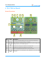
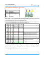
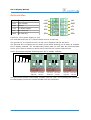
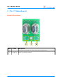
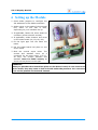
IN-17 Display Module Tubes & Driver Board User Manual October 2013 IN-17 Display Module Table of Contents 1 Features 3 2 Technical Specifications 3 3 Safety Precautions 4 4 IN-17 Driver Board Board Overview I2C Address Selection (SJ1..SJ5) External Bus 5 5 6 7 5 IN-17 Tubes Board Board Overview 8 8 6 Setting up the Module 9 7 Software Overview Initialization Driving the Tubes and LEDs 10 10 10 11 8 Disclaimer 12 9 Contact Information 12 Revision History Date Authors 2013-10-05 Peter S'heeren 2 Description Initial release. User Manual IN-17 Display Module 1 Features ▪ Display module with 2 Russian IN-17 nixie tubes. ▪ I2C interface, module based on two PCA9865 PWM chips. ▪ Fully static, no need to multiplex the tubes. ▪ The brightness of each individually controllable. ▪ The modules can be fitted standard 5.25" drive bay. ▪ Possibility to mount push button switches on the PCB for user control. ▪ RGB backlight LEDs for the tubes. ▪ Backlight is guided to the tubes using light pipes. ▪ Stacked PCB design using low profile MicroMatch connectors. ▪ Power supply +5V DC (logic) / +150 - 170V DC (tubes). ▪ Small size due to the extensive use of SMD components. ▪ Multiple modules can be daisy chained (max. 31 pcs. depending on HV power supply). ▪ The driver board can drive other nixie tubes as well, provided suitable connections are made. digit into is a 2 Technical Specifications IN-17 Display Module Weight 23 g (with IN-17 tubes and mechanical parts) Dimensions 32 mm x 43 mm x 38 mm (W x D x H) IN-17 Driver Board Weight 7g Dimensions 32 mm x 43 mm x 10 mm (W x D x H) IN-17 Tubes Board Weight 15 g (with IN-17 tubes) Dimensions 32 mm x 43 mm x 33 mm (W x D x H) User Manual 3 IN-17 Display Module 3 Safety Precautions SAFETY PRECAUTIONS WHEN THE MODULE IS POWERED ON, DO NOT TOUCH THE DRIVER BOARD OR TUBES BOARD. THE SCREWS AND STANDOFF BETWEEN THE BOARDS ACT AS A CONDUCTOR FOR THE HIGH VOLTAGE ON THE TUBES. AVOID TOUCHING THE SCREWS AND STANDOFF WHEN THE HIGH VOLTAGE IS TURNED ON. DO NOT EXERT FORCE ON THE TUBES, THEY MAY BREAK. DO NOT ILLUMINATE MORE THAN TWO DIGITS WITHIN A TUBE. DRIVING MORE DIGITS MAY HEAT UP AND ULTIMATELY DESTROY THE RESISTORS ON THE TUBES BOARD. 4 User Manual IN-17 Display Module 4 IN-17 Driver Board Board Overview 3 2 1 2 3 6 7 4 Mark Label 1 2 3 5 Description Screw hole for fitting together the driver board and tubes board K3, K4 Screw holes for fixing the board to a surface +HV, GND, Solder pads for connecting and/or chaining the power supply, high +5V, SCL, voltage, I2C bus, and common ground SDA 4 K2 Connector for driving the cathodes in the right tube 5 K1 Connector for driving the cathodes in the left tube 6 7 Pad for conducting the tube power to the driver board SJ1, SJ2, SJ3, SJ4, SJ5 User Manual Solder jumpers for selecting the I2C addresses of the two PWM controllers 5 IN-17 Display Module I2C Address Selection (SJ1..SJ5) SJ5 Mark Description SJ1 A1 selection SJ2 A2 selection SJ3 A3 selection SJ4 A4 selection SJ5 A5 selection SJ3 SJ4 SJ1 SJ2 When a solder jumper is left open (), the selected address line is logically one. When a solder jumper is closed (), the selected address line is logically zero. Use solder wick to open a previously closed solder jump. Address line A0 is hardwired. For the PWM controller of the left tube, A0 is logically zero, while A0 of the PWM controller of the right tube is logically one. SJ SJ SJ SJ SJ 5 4 3 2 1 Address Left Side Address Remarks Right Side 1000 000 b 1000 001 b 1000 010 b 1000 011 b . . . . . . . . . . . . . . . 1101 110 b 1101 111 b 1110 000 b 1110 001 b LED ALL CALL address is 1110 000 b. SUBADR1 by default is 1110 001 b. 1110 010 b 1110 011 b SUBADR2 by default is 1110 010 b. 1110 100 b 1110 101 b SUBADR3 by default is 1110 100 b. 1110 110 b 1110 111 b 1111 000 b 1111 001 b Addresses 1111 0XX b are used for the 10-bit addressing scheme. 1111 010 b 1111 011 b . . . . . . 1111 100 b 1111 101 b Addresses 1111 1XX b are reserved for future use. 1111 110 b 1111 111 b You can't use the configuration in red. The reason is all PWM controllers will respond to the LED ALL CALL address after power-up. You can use the addresses in green providing there are no other I2C slaves on the bus that use these addresses. If you only connect IN-17 modules to the I2C bus, you can safely apply these addresses. Refer to the NXP PCA9685 datasheet for more information. 6 User Manual IN-17 Display Module External Bus Mark Description +HV +HV +HV High voltage GND GND GND Ground +5V 5 V Power supply +5V +5V SCL I2C clock line SCL SCL SDA I2C data line SDA SDA Connect a 170 V power supply to +HV. SCL and SDA levels are 5 V. Connect these lines to an I2C bus. The ground line is common for the 5 V and 170 V supplies and the I2C lines. The external bus is exposed on two sides of the board allowing you to hook up multiple IN-17 display modules. The corresponding solder pads on each side are interconnected hence you're free to choose on which side to connect the various external lines. Here's an example diagram featuring three IN-17 display modules: 170 V GND 5 V SDL SDA 1011 001 b 1011 000 b 1011 011 b 1011 010 b 1011 101 b 1011 100 b Right tube Right tube Right tube Left tube Left tube Left tube The grey boxes denote closed solder jumpers (see SJ1..SJ5). The resulting I2C addresses for each display module are shown beneath the red connectors. User Manual 7 IN-17 Display Module 5 IN-17 Tubes Board Board Overview 2 Mark 1 2 8 Label 1 2 Description Screw hole for fitting the driver board and tubes board S1, K3, S2, Room for optional buttons K4 User Manual IN-17 Display Module 6 Setting up the Module 1. Close solder jumpers to configure the I2C addresses of the PWM controllers. 2. Solder wires on the pads of the external bus, either on one side or both, depending on your intended set up. 3. If applicable, fasten the driver board to a surface (screw holes K3 and K4). 4. If applicable, solder buttons and wires on the tubes board (S1, K3, S2, K4). 5. Fit the light pipe into the holes the tubes. 6. Put the tubes board into place on the driver board. 7. Bind the central screw holes. The screws and standoff serve as a conductor for the tube power (170 V). As such, the screws, washers and standoff must be fitted exactly as shown on the picture to the right. WARNING! When you put the tubes board into place on the driver board, do not exert force on the tubes, they may start to leak or break under the pressure. You can exert force on the printed circuit board instead. User Manual 9 IN-17 Display Module 7 Software Overview From a software point-of-view, the IN-17 display module provides two NXP PCA9685 chips on an I2C bus. The configuration of the solder jumpers (SJ1..SJ5) determines the I2C addresses of the PWM controllers. Refer to the NXP PCA9685 datasheet for more information. Initialization You've to initialize the PWM controllers before programming the PWM channels. We recommend to program the chip's registers as follows (same for both chips): MODE1 Bit Name Value Meaning 7 RESTART 0 Don't clear. 6 EXCLK 0 Use internal clock. 5 AI 1 Enable auto-increment. 4 SLEEP 0 Normal mode (oscillator on). 3 SUB1 0 Don't respond to I2C subaddress 1. 2 SUB2 0 Don't respond to I2C subaddress 2. 1 SUB3 0 Don't respond to I2C subaddress 3. 0 ALLCALL 1 Respond to I2C address LED All Call. Bit Name Value 7..5 - 000b 4 INVRT 0 Output logic state not inverted. 3 OCH 1 Outputs change on I2C ACK after writing all 4 registers of a channel.[1] 2 OUTDRV 1 The LED outputs are configured as a totem pole structure. MODE2 1..0 OUTNE[1..0] 10b Meaning Reserved. When OE=1 the LED outputs are high-impedance. If you set OCH to 0, and you program PWM channels continuously and at great speed, the PWM controller's outputs may become invariant. This happens because the PWM controller needs time to latch new values after it receives the I2C STOP command; if new data comes in too quickly, the PWM controller won't get a chance to start using the values. With OCH set to 1, a PWM channel is programmed directly after I2C ACK and the PWM output changes right away. [1] 10 User Manual IN-17 Display Module Driving the Tubes and LEDs Each PWM controller on the driver board steers one tube's digits and the underlying RGB LED. Each PWM controller incorporates 16 PWM channels. The corresponding output pins are called LED[0..15]. Each PWM channel as a resolution of 12 bits for a value of 0..4095. The PWM controller provides a prescaler setting for adjusting the duration of the PWM cycle. The default value is 30 which translates to 196.9 Hz. There's no need to reprogram this value. The logic of a PWM output is either positive or negative. Positive logic means the target is fully illuminated when the PWM channel is maximally turned on. Negative logic means the target is fully illuminated when the PWM channel is completely turned off. Output Logic Target Output Logic Target LED0 Positive Digit 0 LED8 Positive Digit 2 LED1 Positive Digit 9 LED9 Positive Digit 1 LED2 Positive Digit 8 LED10 Negative Blue LED3 Positive Digit 7 LED11 Negative Red LED4 Positive Digit 6 LED12 Negative Green LED5 Positive Digit 5 LED13 Not connected LED6 Positive Digit 4 LED14 Not connected LED7 Positive Digit 3 LED15 Not connected You may illuminate two or more digits and once. However, the more digits you drive, the more current will flow through the resistor next to the tube. If too much current flows through the resistor, it will heat up too much and break. The recommended limit is two fully illuminated digits, or the equivalent spread over more digits. User Manual 11 IN-17 Display Module 8 Disclaimer Axiris products are not designed, authorized or warranted to be suitable for use in space, nautical, space, military, medical, life-critical or safety-critical devices or equipment. Axiris products are not designed, authorized or warranted to be suitable for use in applications where failure or malfunction of an Axiris product can result in personal injury, death, property damage or environmental damage. Axiris accepts no liability for inclusion or use of Axiris products in such applications and such inclusion or use is at the customer's own risk. Should the customer use Axiris products for such application, the customer shall indemnify and hold Axiris harmless against all claims and damages. 9 Contact Information Official website: http://www.axiris.be/ 12 User Manual