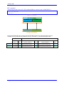
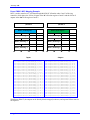
1
^1 USER MANUAL ^2 Accessory 65E ^3Digital I/O – Sinking Inputs, Sourcing Outputs ^4 3Ax-603575-xUxx ^5 February 14, 2015 DELTA TAU Data Systems, Inc. NEW IDEAS IN MOTION … Single Source Machine Control ……………………………………………..…...………………. Power // Flexibility // Ease of Use 21314 Lassen St. Chatsworth, CA 91311 // Tel. (818) 998-2095 Fax. (818) 998-7807 // www.deltatau.com Accessory 65E Copyright Information © 2015 Delta Tau Data Systems, Inc. All rights reserved. This document is furnished for the customers of Delta Tau Data Systems, Inc. Other uses are unauthorized without written permission of Delta Tau Data Systems, Inc. Information contained in this manual may be updated from time-to-time due to product improvements, etc., and may not conform in every respect to former issues. To report errors or inconsistencies, call or email: Delta Tau Data Systems, Inc. Technical Support Phone: (818) 717-5656 Fax: (818) 998-7807 Email: [email protected] Website: http://www.deltatau.com Operating Conditions All Delta Tau Data Systems, Inc. motion controller products, accessories, and amplifiers contain static sensitive components that can be damaged by incorrect handling. When installing or handling Delta Tau Data Systems, Inc. products, avoid contact with highly insulated materials. Only qualified personnel should be allowed to handle this equipment. In the case of industrial applications, we expect our products to be protected from hazardous or conductive materials and/or environments that could cause harm to the controller by damaging components or causing electrical shorts. When our products are used in an industrial environment, install them into an industrial electrical cabinet or industrial PC to protect them from excessive or corrosive moisture, abnormal ambient temperatures, and conductive materials. If Delta Tau Data Systems, Inc. products are directly exposed to hazardous or conductive materials and/or environments, we cannot guarantee their operation. A Warning identifies hazards that could result in personal injury or death. It precedes the discussion of interest. WARNING A Caution identifies hazards that could result in equipment damage. It precedes the discussion of interest. Caution A Note identifies information critical to the understanding or use of the equipment. It follows the discussion of interest. Note Accessory 65E REVISION HISTORY REV. 1 2 3 4 5 6 7 DESCRIPTION Added CE Declaration Revs. To J1, J2, Pins 8, 15 Reformatted Schematics Updated Max Current Output Added UL seal, updated agency approval Added Power PMAC/MACRO Reformatted manual Corrected DIP switch settings DATE CHG APPVD 06/07/06 05/11/07 01/18/08 01/29/08 10/01/09 CP CP CP CP CP SF AO SF SM SF 02/24/14 RN RN 02/03/15 RN RN Accessory 65E Table of Contents INTRODUCTION ................................................................................................................................. 7 SPECIFICATIONS ............................................................................................................................... 8 Environmental Specifications .................................................................................................................. 8 Electrical Specifications .......................................................................................................................... 8 Power Requirements ........................................................................................................................... 8 Fuse ................................................................................................................................................... 8 Input Drivers ........................................................................................................................................... 8 Output Drivers......................................................................................................................................... 8 Physical Specifications ............................................................................................................................ 9 Terminal Block Layout ....................................................................................................................... 9 D-Sub Layout ..................................................................................................................................... 9 Agency Approval and Safety ................................................................................................................. 10 ADDRESSING THE ACC-65E........................................................................................................... 12 Address Select DIP Switch SW1 ........................................................................................................... 12 Legacy MACRO Dip Switch Settings .................................................................................................... 13 Hardware Address Limitations .............................................................................................................. 13 USING THE ACC-65E WITH POWER UMAC................................................................................ 15 Declaring Pointers to I/O Structure Elements ......................................................................................... 15 USING THE ACC-65E WITH TURBO UMAC ................................................................................ 16 Assigning M-Variables to I/O Memory Locations .................................................................................. 16 Configuring the Control Word ............................................................................................................... 16 USING THE ACC-65E WITH MACRO ............................................................................................ 17 MACRO16 I/O Node Addressing .......................................................................................................... 18 Ring Controller I/O Node Addressing .................................................................................................... 20 Turbo PMAC2 I/O Node Addressing ................................................................................................. 20 Power PMAC2 I/O Node Addressing ................................................................................................ 21 Power PMAC3 I/O Node Addressing ................................................................................................ 23 Configuring MACRO I/O Transfers ...................................................................................................... 25 MS{anynode},MI160 ........................................................................................................................ 26 MS{anynode},MI71 .......................................................................................................................... 30 MS{anynode},MI69/MI70 ................................................................................................................. 34 Accessing the Transferred Data ............................................................................................................. 37 Outputs Mirror Image Concept ......................................................................................................... 37 Turbo PMAC2 MI160 Mapping Example .......................................................................................... 38 Turbo PMAC2 MI71 Mapping Example............................................................................................ 40 Turbo PMAC2 MI69/70 Mapping Example ....................................................................................... 42 Power PMAC2 MI160 Mapping Example ......................................................................................... 44 Power PMAC2 MI71 Mapping Example ........................................................................................... 46 Power PMAC2 MI69/70 Mapping Example ...................................................................................... 48 Power PMAC3 MI160 Mapping Example ......................................................................................... 50 Table of Contents v Accessory 65E Power PMAC3 MI71 Mapping Example ........................................................................................... 51 Power PMAC3 MI69/70 Mapping Example ...................................................................................... 52 Configuring the Control Word for MACRO ........................................................................................... 53 CONNECTOR PINOUTS AND WIRING ......................................................................................... 54 Terminal Block Connectors ................................................................................................................... 54 Top: Inputs ....................................................................................................................................... 54 Bottom: Outputs ............................................................................................................................... 55 TB Wiring Diagram .......................................................................................................................... 56 D-Sub Connectors ................................................................................................................................. 57 Top: Inputs ....................................................................................................................................... 57 Bottom: Outputs ............................................................................................................................... 57 D-Sub Wiring diagram ..................................................................................................................... 58 P1: UMAC Bus (UBUS) Connector ....................................................................................................... 59 APPENDIX A: E-POINT JUMPERS ................................................................................................. 60 APPENDIX B: SCHEMATICS .......................................................................................................... 61 APPENDIX C: USING THE ACC-65E IN C ..................................................................................... 63 ACC-65E C Library.......................................................................................................................... 63 Locations for the C Files .................................................................................................................. 64 Function Descriptions ...................................................................................................................... 66 Example ........................................................................................................................................... 67 Table of Contents vi Accessory 65E INTRODUCTION The accessory 65E (ACC-65E) is a general purpose digital input and output card. It provides 24 inputs and 24 outputs of self-protected, optically isolated sinking inputs and sourcing outputs. The ACC-65E is a 3U Euro style card intended to plug into the UMAC BUS backplane. It can be used with the: Turbo UMAC CPU Power UMAC CPU MACRO UMAC Station (MACRO16 CPU, PMAC2 or PMAC3 Style) Introduction 7 Accessory 65E SPECIFICATIONS Environmental Specifications Description Specification Operating Temperature 0°C to 45°C Storage Temperature -25°C to 70°C Humidity 10% to 95 % Notes Non-Condensing Electrical Specifications Power Requirements Whether providing the ACC-65E with power from the 3U backplane bus or externally (standalone mode) through TB1, the power requirements (± 10%) are: +5 V @ 0.38 A +24 V @ 0.60 A +24 V @ 8.00 A Note (Board Logic Input) (Per Output Pin) (Maximum current when using all outputs simultaneously) TB1 is a 2-pin 5V connector on the base board (used for standalone operation), not to be confused with the 12-pin TB1 connector on either of the I/O mezzanine boards. Fuse Manufacturer Specification Bussmann 125 V @ 20 A Delta Tau Part Number MDA 20A Input Drivers The inputs to the ACC-65E have an activation range from 12V to 24V. Due to the self-protecting circuitry, the inputs can only be configured as sinking. Although self-protecting, no more than 33VDC should be applied to any I/O pin. This is a limitation of the protective circuitry which includes MMBZ33VALT1 Zener diodes. Output Drivers The output drivers use the Diodes Inc. Zetex ZXMS6006DG chip. The current drawn from each output line should be limited to 600 mA at voltage levels between 12 VDC and 24 VDC and no more than 8 Amps total for all outputs simultaneously. Specifications 8 Accessory 65E Physical Specifications Terminal Block Layout Pin #1 0.9 6.30 TB1 TB2 3.94 5.08 TB2 TB1 Pin #1 D-Sub Layout 0.9 6.30 J1 J2 3.94 5.08 J2 Specifications J1 9 Accessory 65E Description Specification Notes Length: 16.256 cm (6.4 in.) Height: 10 cm (3.94 in.) Width: 2.03 cm (0.8 in.) Dimensions Weight w/o Option 1A 180 g Terminal Block Connectors FRONT-MC1,5/12-ST3,81 FRONT-MC1,5/5-ST3,81 FRONT-MC1,5/3-ST3,81 DB Option Connectors Note Front Plate included Terminal Blocks from Phoenix Contact. UL 94V-0 DB15 Female UL 94V-0 The width is the width of the front plate. The length and height are the dimensions of the PCB. See Layout section for physical dimensions. Agency Approval and Safety Item Description CE Mark Full Compliance Safety EN55011 Class A Group 1 EN61000-3-2 Class A EN61000-3-3 EN61000-4-2 EN61000-4-3 EN61000-4-4 EN61000-4-5 EN61000-4-6 EN61000-4-11 EN 61010-1 UL UL 61010-1 File E314517 cUL CAN/CSA C22.2 No. 1010.1-92 File E314517 EMC Specifications 10 Accessory 65E Application of Council Directive: 89/336/EEC, 72/23/EEC Manufacturers Name: Manufacturers Address: Delta Tau Data Systems, Inc. 21314 Lassen Street Chatsworth, CA 91311 USA We, Delta Tau Data Systems, Inc. hereby declare that the product Product Name: Accessory 65E Model Number: 603575 And all of its options conforms to the following standards: EN61326: 1997 Electrical equipment for measurement, control, and laboratory useEMC requirements EN55011: 1998 Limits and methods of measurements of radio disturbance characteristics of information technology equipment Electrical equipment for measurement, control, and laboratory use- Safety requirements Limits for harmonic current emissions. Criteria A EN61010-1 EN61000-3-2 :1995 A14:1998 EN61000-3-3: 1995 EN61000-4-2:1995 A1: 1998 EN61000-4-3: 1995 A1: 1998 EN61000-4-4: 1995 EN61000-4-5: 1995 EN61000-4-6: 1996 EN61000-4-11: 1994 Date Issued: Place Issued: Limitation of voltage fluctuations and flicker in low-voltage supply systems for equipment with rated current 16A. Criteria B. Electro Static Discharge immunity test. Criteria B Radiated, radio-frequency, electromagnetic field immunity test. Criteria A Electrical fast transients/burst immunity test. Criteria B Surge Test. Criteria B Conducted immunity test. Criteria A Voltage dips test. Criteria B and C 11 May 2006 Chatsworth, California USA Mark of Compliance Specifications 11 Accessory 65E ADDRESSING THE ACC-65E Address Select DIP Switch SW1 The switch SW1 selects the starting address location for the first I/O gate on the ACC-65E. The following table shows the dip switch settings for the Turbo, Power, and MACRO Station settings: Base Address Chip Select CS10 CS12 CS14 CS16 SW1 Positions POWER TURBO MACRO 4 3 2 1 Y:$78C00 ON ON ON ON ON ON 4 ON ON ON OFF ON ON $A10000 8 ON ON OFF ON ON ON Y:$B800 $A18000 12 ON ON OFF OFF ON ON Y:$78D00 Y:$8840 $B00000 1 ON ON ON ON ON OFF Y:$79D00 Y:$9840 $B08000 5 ON ON ON OFF ON OFF Y:$7AD00 Y:$A840 $B10000 9 ON ON OFF ON ON OFF Y:$7BD00 Y:$B840 $B18000 13 ON ON OFF OFF ON OFF Y:$78E00 Y:$8880 $C00000 2 ON ON ON ON OFF ON Y:$79E00 Y:$9880 $C08000 6 ON ON ON OFF OFF ON Y:$7AE00 Y:$A880 $C10000 10 ON ON OFF ON OFF ON Y:$7BE00 Y:$B880 $C18000 14 ON ON OFF OFF OFF ON Y:$78F00 Y:$88C0 $D00000 3 ON ON ON ON Y:$79F00 Y:$98C0 $D08000 7 ON ON ON OFF OFF OFF Y:$7AF00 Y:$A8C0 $D10000 11 ON ON OFF Y:$7BF00 Y:$B8C0 $D18000 15 ON ON OFF OFF OFF OFF I/O Base Offset Index ACC-65E[n] Y:$8800 $A00000 0 Y:$79C00 Y:$9800 $A08000 Y:$7AC00 Y:$A800 Y:$7BC00 6 5 ON OFF OFF OFF OFF ON designates Closed. OFF designates Open. Factory default is all ON. Note Addressing The ACC-65E 12 Accessory 65E Legacy MACRO Dip Switch Settings SW1 Positions 5 4 Chip Select Base Address (Alternate) 6 10 12 14 16 Y:$B800 (Y:$FFE0) Y:$B840 (Y:$FFE8) Y:$B880 (Y:$FFF0) Y:$B8C0 (Y:$FFF8) ON (OFF) ON (OFF) ON (OFF) ON (OFF) ON (OFF) ON (OFF) ON (OFF) ON (OFF) OFF OFF OFF ON 3 2 1 OFF OFF OFF ON ON ON OFF OFF ON OFF ON OFF The Legacy Macro base addresses are double mapped. Set SW1 positions 5 & 6 to OFF if the alternate addressing is desired. Note Hardware Address Limitations Historically, two types of accessory cards have been designed for the UMAC 3U bus type rack: type A and type B cards. They can be sorted out as follows: Name Type Category Possible Number of Base Addresses Maximum Number of cards in 1 rack ACC-9E ACC-10E ACC-11E ACC-12E A A A A General I/O General I/O General I/O General I/O 4 4 4 4 10 ACC-53E ACC-57E ACC-58E ACC-59E B B B B Feedback Feedback Feedback Analog I/O 12 12 12 12 12 ACC-14E ACC-28E ACC-36E ACC-65E ACC-66E ACC-67E ACC-68E B B B B B B B General I/O Analog I/O Analog I/O General I/O General I/O General I/O General I/O 16 16 16 16 16 16 16 16 ACC-84E B Feedback 12 12 Addressing The ACC-65E 13 Accessory 65E Addressing Type A and Type B accessory cards in a UMAC or MACRO station rack requires attention to the following set of rules: Populating Rack with Type A Cards Only (no conflicts) In this case, the card(s) can potentially use any available Address/Chip Select. Note The type A cards have only one base address per chip select (CS10, CS12, and CS14). Each card can be set up (jumper settings) to use the low, middle, or high byte of a specific base address. This makes it possible to populate a single rack with 9 (3 bases x 3 byte locations) Type A accessory cards. A fourth address is available at CS16 in which only the high byte can be used, thus making the maximum 10 Type A accessory cards. Populating Rack with Type B Cards Only (no conflicts) In this case, the card(s) can potentially use any available Address/Chip Select. Populating Rack with Type A & Type B Cards (possible conflicts) Typically, Type A and Type B cards should not share the same Chip Select. If this configuration is possible, then the following rules apply: Type A and Type B Feedback Cards Type A cards cannot share the same base address as Type B Feedback cards. Type A and Type B General I/O Cards Type A cards can share base addresses with Type B general I/O cards; however, in this case, Type B cards naturally use the lower byte (default), and Type A cards must be set to the middle/high byte of the selected base address. Type A Cards and Type B Analog Cards Type A cards can share base addresses with Type B analog I/O cards; however, in this case, Type B cards naturally use the middle/high bytes (default), so Type A cards should be set to the low byte of the selected base address. Note The above conflicts only occur with the first base address in each Chip Select of the Type B cards (i.e. $78C00, $78D00, $78E00, and $78F00). Conflicts can more simply be avoided by using only the second to fourth addresses of each Chip Select. Addressing The ACC-65E 14 Accessory 65E USING THE ACC-65E WITH POWER UMAC Using the ACC-65E with Power UMAC requires: Knowing and configuring the index (address offset) of the card Declaring pointers, with user given names, to the appropriate I/O structure elements Declaring Pointers to I/O Structure Elements Mapping an ACC-65E at index 0, for example, with user configurable pointer names: Inputs Outputs PTR PTR PTR PTR PTR PTR PTR PTR Input1->ACC65E[0].DataReg[0].0.1; Input2->ACC65E[0].DataReg[0].1.1; Input3->ACC65E[0].DataReg[0].2.1; Input4->ACC65E[0].DataReg[0].3.1; Input5->ACC65E[0].DataReg[0].4.1; Input6->ACC65E[0].DataReg[0].5.1; Input7->ACC65E[0].DataReg[0].6.1; Input8->ACC65E[0].DataReg[0].7.1; PTR PTR PTR PTR PTR PTR PTR PTR Output1->ACC65E[0].DataReg[3].0.1; Output2->ACC65E[0].DataReg[3].1.1; Output3->ACC65E[0].DataReg[3].2.1; Output4->ACC65E[0].DataReg[3].3.1; Output5->ACC65E[0].DataReg[3].4.1; Output6->ACC65E[0].DataReg[3].5.1; Output7->ACC65E[0].DataReg[3].6.1; Output8->ACC65E[0].DataReg[3].7.1; PTR PTR PTR PTR PTR PTR PTR PTR Input9->ACC65E[0].DataReg[1].0.1; Input10->ACC65E[0].DataReg[1].1.1; Input11->ACC65E[0].DataReg[1].2.1; Input12->ACC65E[0].DataReg[1].3.1; Input13->ACC65E[0].DataReg[1].4.1; Input14->ACC65E[0].DataReg[1].5.1; Input15->ACC65E[0].DataReg[1].6.1; Input16->ACC65E[0].DataReg[1].7.1; PTR PTR PTR PTR PTR PTR PTR PTR Output9->ACC65E[0].DataReg[4].0.1; Output10->ACC65E[0].DataReg[4].1.1; Output11->ACC65E[0].DataReg[4].2.1; Output12->ACC65E[0].DataReg[4].3.1; Output13->ACC65E[0].DataReg[4].4.1; Output14->ACC65E[0].DataReg[4].5.1; Output15->ACC65E[0].DataReg[4].6.1; Output16->ACC65E[0].DataReg[4].7.1; PTR PTR PTR PTR PTR PTR PTR PTR Input17->ACC65E[0].DataReg[2].0.1; Input18->ACC65E[0].DataReg[2].1.1; Input19->ACC65E[0].DataReg[2].2.1; Input20->ACC65E[0].DataReg[2].3.1; Input21->ACC65E[0].DataReg[2].4.1; Input22->ACC65E[0].DataReg[2].5.1; Input23->ACC65E[0].DataReg[2].6.1; Input24->ACC65E[0].DataReg[2].7.1; PTR PTR PTR PTR PTR PTR PTR PTR Output17->ACC65E[0].DataReg[5].0.1; Output18->ACC65E[0].DataReg[5].1.1; Output19->ACC65E[0].DataReg[5].2.1; Output20->ACC65E[0].DataReg[5].3.1; Output21->ACC65E[0].DataReg[5].4.1; Output22->ACC65E[0].DataReg[5].5.1; Output23->ACC65E[0].DataReg[5].6.1; Output24->ACC65E[0].DataReg[5].7.1; Typically, these pointers would be put in a “Global Includes” file. Note To switch/add definitions to a different card, change the ACC65E[0] to ACC65E[n], where n is the card index set by the dip switch settings. With Power PMAC, the control word is set up automatically by the firmware with ACC65E[n].CtrlReg = 7. Note Using the ACC-65E with Power UMAC 15 Accessory 65E USING THE ACC-65E WITH TURBO UMAC Using the ACC-65E with Turbo UMAC requires: Knowing (configuring) the base address of the card Pointing M-Variables to the appropriate I/O memory locations Configuring the control word Assigning M-Variables to I/O Memory Locations Mapping an ACC-65E at $78C00, for example, with user configurable M-Variable numbers and name substitutions: Inputs Outputs #define #define #define #define #define #define #define #define Input1 Input2 Input3 Input4 Input5 Input6 Input7 Input8 M7001 M7002 M7003 M7004 M7005 M7006 M7007 M7008 Input1->Y:$078C00,0,1 Input2->Y:$078C00,1,1 Input3->Y:$078C00,2,1 Input4->Y:$078C00,3,1 Input5->Y:$078C00,4,1 Input6->Y:$078C00,5,1 Input7->Y:$078C00,6,1 Input8->Y:$078C00,7,1 #define #define #define #define #define #define #define #define Output1 Output2 Output3 Output4 Output5 Output6 Output7 Output8 M7025 M7026 M7027 M7028 M7029 M7030 M7031 M7032 Output1->Y:$078C03,0,1 Output2->Y:$078C03,1,1 Output3->Y:$078C03,2,1 Output4->Y:$078C03,3,1 Output5->Y:$078C03,4,1 Output6->Y:$078C03,5,1 Output7->Y:$078C03,6,1 Output8->Y:$078C03,7,1 #define #define #define #define #define #define #define #define Input9 Input10 Input11 Input12 Input13 Input14 Input15 Input16 M7009 M7010 M7011 M7012 M7013 M7014 M7015 M7016 Input9->Y:$078C01,0,1 Input10->Y:$078C01,1,1 Input11->Y:$078C01,2,1 Input12->Y:$078C01,3,1 Input13->Y:$078C01,4,1 Input14->Y:$078C01,5,1 Input15->Y:$078C01,6,1 Input16->Y:$078C01,7,1 #define #define #define #define #define #define #define #define Output9 Output10 Output11 Output12 Output13 Output14 Output15 Output16 M7033 M7034 M7035 M7036 M7037 M7038 M7039 M7040 Output9->Y:$078C04,0,1 Output10->Y:$078C04,1,1 Output11->Y:$078C04,2,1 Output12->Y:$078C04,3,1 Output13->Y:$078C04,4,1 Output14->Y:$078C04,5,1 Output15->Y:$078C04,6,1 Output16->Y:$078C04,7,1 #define #define #define #define #define #define #define #define Input17 Input18 Input19 Input20 Input21 Input22 Input23 Input24 M7017 M7018 M7019 M7020 M7021 M7022 M7023 M7024 Input17->Y:$078C02,0,1 Input18->Y:$078C02,1,1 Input19->Y:$078C02,2,1 Input20->Y:$078C02,3,1 Input21->Y:$078C02,4,1 Input22->Y:$078C02,5,1 Input23->Y:$078C02,6,1 Input24->Y:$078C02,7,1 #define #define #define #define #define #define #define #define Output17 Output18 Output19 Output20 Output21 Output22 Output23 Output24 M7041 M7042 M7043 M7044 M7045 M7046 M7047 M7048 Output17->Y:$078C05,0,1 Output18->Y:$078C05,1,1 Output19->Y:$078C05,2,1 Output20->Y:$078C05,3,1 Output21->Y:$078C05,4,1 Output22->Y:$078C05,5,1 Output23->Y:$078C05,6,1 Output24->Y:$078C05,7,1 Note To address a different card, replace the xx digits in the address locations $07xx00 to $07xx05 to correspond to the base address configured by the dip switch settings. Configuring the Control Word With Turbo PMAC, the control word must be set to 7. This is done by writing (once on power-up) to the control register which is at base address + 7, bits [7:0]. M7000->Y:$078C07,0,8 // For base address $78C00 Open PLC 1 Clear M7000 = 7 Disable PLC 1 Close Using the ACC-65E with Turbo UMAC 16 Accessory 65E USING THE ACC-65E WITH MACRO In a MACRO configuration, the ACC-65E resides typically in a UMAC MACRO Station with a MACRO8 (legacy) or MACRO16 CPU. The ring controller can be either a Turbo or a Power PMAC. Turbo Brick family Turbo UMAC with ACC-5E Turbo UltraLite Power PMAC ring controllers: Power Brick family Power UMAC with ACC-5E Power UMAC with ACC-5E3 Power EtherLite IN MACRO16 ACC-65E ACC-65E OUT Turbo PMAC ring controllers: ... MACRO16 ACC-65E ACC-65E UMAC MACRO Station #2 ... IN Ring Controller OUT OUT IN UMAC MACRO Station #1 Generally, the user’s goal is to transfer the ACC-65E I/O data (48 bits per card) from/to the ring controller by reading the 24-bits of inputs and writing to the 24-bits of outputs. This I/O data transfer is accomplished using I/O nodes; therefore, it is essential to know: Which I/O nodes are used Which MACRO station I/O node addresses correspond to which Ring Controller I/O node addresses Using the ACC-65E With MACRO 17 Accessory 65E MACRO16 I/O Node Addressing A MACRO IC consists of a number of auxiliary, servo, and I/O nodes: Auxiliary nodes are Master/Control registers and are for internal firmware use. Servo nodes carry information such as feedback, commands, and flags for motor control. I/O nodes are by default unoccupied and are configurable for transferring miscellaneous data. The MACRO16 CPU is populated with two PMAC2 style MACRO ICs, each consisting of 16 nodes: 2 auxiliary, 8 servo, and 6 I/O nodes (the legacy MACRO8 has only one IC). I/O Nodes Node 15 14 13 12 11 10 9 Auxiliary Nodes 8 7 6 5 4 3 2 1 0 1 0 Servo Nodes Each I/O node consists of one 24-bit and three 16-bit (upper) data registers: 13 12 11 10 24-bit 1st 16-bit 2nd 16-bit 3rd 16-bit 24-bit 1st 16-bit 2nd 16-bit 3rd 16-bit 9 8 7 6 24-bit 1st 16-bit 2nd 16-bit 3rd 16-bit 24-bit 1st 16-bit 2nd 16-bit 3rd 16-bit 5 4 3 2 24-bit 1st 16-bit 2nd 16-bit 3rd 16-bit 24-bit 1st 16-bit 2nd 16-bit 3rd 16-bit The MACRO8 CPU is populated with only 1 PMAC2 Style MACRO IC (IC# 0). Note Using the ACC-65E With MACRO 18 Accessory 65E The I/O node data register addresses ($C0XX) for the two MACRO ICs on a station are: MACRO Station IC #0 Node 2 3 6 7 10 11 24-bit X:$C0A0 X:$C0A4 X:$C0A8 X:$C0AC X:$C0B0 X:$C0B4 16-bit X:$C0A1 X:$C0A5 X:$C0A9 X:$C0AD X:$C0B1 X:$C0B5 16-bit X:$C0A2 X:$C0A6 X:$C0AA X:$C0AE X:$C0B2 X:$C0B6 16-bit X:$C0A3 X:$C0A7 X:$C0AB X:$C0AF X:$C0B3 X:$C0B7 MACRO Station IC #1 Node 2 3 6 7 10 11 24-bit X:$C0E0 X:$C0E4 X:$C0E8 X:$C0EC X:$C0F0 X:$C0F4 16-bit X:$C0E1 X:$C0E5 X:$C0E9 X:$C0ED X:$C0F1 X:$C0F5 16-bit X:$C0E2 X:$C0E6 X:$C0EA X:$C0EE X:$C0F2 X:$C0F6 16-bit X:$C0E3 X:$C0E7 X:$C0EB X:$C0EF X:$C0F3 X:$C0F7 Note Note I/O nodes which will be chosen to transfer the ACC-65E(s) data are configurable and chosen by the user depending on availability and I/O node management in the MACRO station. Non-Turbo PMAC2 Ultralite (legacy) I/O node addresses are the same as MACRO Station IC# 0 node registers. For instance, addresses on the ring controller start at $C0A0, instead of at $78420 as seen in the following section. Using the ACC-65E With MACRO 19 Accessory 65E Ring Controller I/O Node Addressing Turbo PMAC2 I/O Node Addressing Turbo ring controllers interface with PMAC2 Style MACRO ICs. The data resides in the bit fields illustrated on the right: Turbo PMAC2 I/O Node 24-bit Register Turbo ring controllers can be populated with up to 4 PMAC2 style MACRO ICs (reported by I4902). Below are the I/O node addresses ($7XXXX) for each of the PMAC2 Style MACRO ICs: 16-bit Register 1 16-bit Register 2 16-bit Register 3 23 15 7 0 Turbo Ring Controller MACRO IC #0 Node Registers Station I/O Node# 2 3 6 7 10 11 Ring Controller I/O Node# 2 3 6 7 10 11 24-bit X:$78420 X:$78424 X:$78428 X:$7842C X:$78430 X:$78434 16-bit X:$78421 X:$78425 X:$78429 X:$7842D X:$78431 X:$78435 16-bit X:$78422 X:$78426 X:$7842A X:$7842E X:$78432 X:$78436 16-bit X:$78423 X:$78427 X:$7842B X:$7842F X:$78433 X:$78437 Turbo Ring Controller MACRO IC #1 Node Registers Station I/O Node# 2 3 6 7 10 11 Ring Controller I/O Node# 18 19 22 23 26 27 24-bit X:$79420 X:$79424 X:$79428 X:$7942C X:$79430 X:$79434 16-bit X:$79421 X:$79425 X:$79429 X:$7942D X:$79431 X:$79435 16-bit X:$79422 X:$79426 X:$7942A X:$7942E X:$79432 X:$79436 16-bit X:$79423 X:$79427 X:$7942B X:$7942F X:$79433 X:$79437 Turbo Ring Controller MACRO IC #2 Node Registers Station I/O Node# 2 3 6 7 10 11 Ring Controller I/O Node# 34 35 38 39 42 43 24-bit X:$7A420 X:$7A424 X:$7A428 X:$7A42C X:$7A430 X:$7A434 16-bit X:$7A421 X:$7A425 X:$7A429 X:$7A42D X:$7A431 X:$7A435 16-bit X:$7A422 X:$7A426 X:$7A42A X:$7A42E X:$7A432 X:$7A436 16-bit X:$7A423 X:$7A427 X:$7A42B X:$7A42F X:$7A433 X:$7A437 Turbo Ring Controller MACRO IC #3 Node Registers Station I/O Node# 2 3 6 7 10 11 Ring Controller I/O Node# 50 51 54 55 58 59 24-bit X:$7B420 X:$7B424 X:$7B428 X:$7B42C X:$7B430 X:$7B434 16-bit X:$7B421 X:$7B425 X:$7B429 X:$7B42D X:$7B431 X:$7B435 16-bit X:$7B422 X:$7B426 X:$7B42A X:$7B42E X:$7B432 X:$7B436 16-bit X:$7B423 X:$7B427 X:$7B42B X:$7B42F X:$7B433 X:$7B437 Using the ACC-65E With MACRO 20 Accessory 65E Power PMAC2 I/O Node Addressing PMAC2 Style I/O Node 24-bit Register The Power PMAC can interface with the ACC-5E which carries PMAC2 Style MACRO ICs. 16-bit Register 1 The PMAC2 Style MACRO IC I/O node data registers reside in the bit fields illustrated on the right: 16-bit Register 2 16-bit Register 3 23 15 7 0 And the corresponding structure elements: Where: Structure Element Data Register Gate2[i].Macro[j][0] 24 bits Gate2[i].Macro[j][1] 16 bits Gate2[i].Macro[j][2] 16 bits Gate2[i].Macro[j][3] 16 bits i is the PMAC2 Style MACRO IC index j is the I/O node number. Bitwise mapping, into the PMAC2 Style MACRO structure elements requires Power PMAC firmware version 1.5.8.215 or newer. Note Using the ACC-65E With MACRO 21 Accessory 65E The tables below show I/O Node numbers of the 4 PMAC2 Style MACRO ICs: Gate2[0] Station I/O Node# 2 3 6 7 10 11 Ring Controller I/O Node [j] 2 3 6 7 10 11 Gate2[1] Station I/O Node# 2 3 6 7 11 12 Ring Controller I/O Node [j] 18 19 22 23 26 27 Gate2[2] Station I/O Node# 2 3 6 7 10 11 Ring Controller I/O Node [j] 34 35 38 39 42 43 Gate2[3] Station I/O Node# 2 3 6 7 11 12 Ring Controller I/O Node [j] 50 51 54 55 58 59 Using the ACC-65E With MACRO 22 Accessory 65E Power PMAC3 I/O Node Addressing A PMAC3 style MACRO IC consists of 32 nodes: 4 auxiliary, 16 servo, and 12 I/O nodes. One or more of these ICs can be found in the following hardware: Power Brick Family Power UMAC with ACC-5E3 Power EtherLite I/O Nodes Node 31 30 29 28 27 26 Auxiliary Nodes 25 24 23 22 I/O Nodes 21 20 19 18 17 16 15 14 13 12 11 Auxiliary Nodes Servo Nodes 10 9 8 7 6 5 4 3 2 Servo Nodes Bank B Bank A The Power PMAC can have up to 16 PMAC3 Style MACRO ICs. ICs present are reported by the variable Macro.IC3s. Note A PMAC3 Style MACRO IC I/O node consists of 4 data registers: 1 x 24-bit and 3 x 16-bit residing in the following bit fields: PMAC3 Style I/O Node 24-bit Register 16-bit Register 1 16-bit Register 2 16-bit Register 3 31 23 Using the ACC-65E With MACRO 15 7 0 23 1 0 Accessory 65E With the PMAC3 Style MACRO ICs, the I/O node data registers are typically accessed using structure elements, which can be inputs or outputs for either bank: Bank B Bank A Inputs Outputs Inputs Data Register Outputs Gate3[i].MacroInB[j][0] Gate3[i].MacroOutB[j][0] Gate3[i].MacroInA[j][0] Gate3[i].MacroOutA[j][0] 24-bit Gate3[i].MacroInB[j][1] Gate3[i].MacroOutB[j][1] Gate3[i].MacroInA[j][1] Gate3[i].MacroOutA[j][1] 1st 16-bit Gate3[i].MacroInB[j][2] Gate3[i].MacroOutB[j][2] Gate3[i].MacroInA[j][2] Gate3[i].MacroOutA[j][2] 2nd 16-bit Gate3[i].MacroInB[j][3] Gate3[i].MacroOutB[j][3] Gate3[i].MacroInA[j][3] Gate3[i].MacroOutA[j][3] 3rd 16-bit Where: i is the PMAC3 Style MACRO IC index j is the I/O node number. Bitwise mapping into the PMAC3 Style MACRO structure elements requires Power PMAC firmware version 1.5.8.215 or newer. Note Below are example tables showing I/O Node numbers of the first 4 PMAC3 Style MACRO ICs: Gate3[0] Bank A Bank B Station Node# 2 3 6 7 10 11 2 3 6 7 11 12 Ring Controller I/O Node [j] 2 3 6 7 10 11 18 19 22 23 26 27 Gate3[1] Bank A Bank B Station Node# 2 3 6 7 10 11 2 3 6 7 11 12 Ring Controller I/O Node [j] 34 35 38 39 42 43 50 51 54 55 58 59 Gate3[2] Bank A Bank B Station Node# 2 3 6 7 10 11 2 3 6 7 11 12 Ring Controller I/O Node [j] 66 67 70 71 74 75 82 83 86 87 90 91 Gate3[3] Bank A Bank B Station Node# 2 3 6 7 10 11 2 3 6 7 11 12 Ring Controller I/O Node [j] 98 99 102 103 106 107 114 115 118 119 122 123 Using the ACC-65E With MACRO 24 Accessory 65E Configuring MACRO I/O Transfers Having set up the following: Ring Controller MACRO communication for ASCII and MS commands I6840 with Turbo PMAC2 Gate2[i].MacroMode with Power PMAC2 Gate3[i].MacroModeA and Gate3[i].MacroModeB with Power PMAC3 MACRO Station MACRO communication for ASCII and MS commands MI996 Enabled the chosen I/O nodes on the ring controller I6841 with Turbo PMAC2 Gate2[i].MacroEnable with Power PMAC2 Gate3[i].MacroEnableA and Gate3[i].MacroEnableB with Power PMAC3 Enabled the corresponding I/O nodes on the MACRO station IC MS{anynode},MI975 Typically, masked with the enabled I/O node(s) E.g. MS2,MI975=$4 enables transfers using I/O node number 2. Set up the I/O Data Transfer Period MS{anynode},MI19 Typically = 4 The ACC-65E(s) I/O data should now be available to transfer to/from the ring controller. Each ACC-65E possesses 48 bits (24 in/24 out) of data to be transferred. Depending on the number of cards in the MACRO station and I/O nodes available, one or more of the following methods can be used, stated in the order of simplicity: MS{anynode},MI160 48-bit transfer into a 1 x 24-bit data register (uses 1 x I/O node) MS{anynode},MI71 48-bit transfer into 2 x 24-bit data registers (uses 2 x I/O nodes) MS{anynode},MI69/MI70 48-bit transfer into 3 x 16-bit data registers (uses 1 x I/O nodes) {anynode} refers to any activated node on a particular MACRO IC. Note MS{anynode},MI160 newer. requires MACRO16 CPU firmware 1.204 or Note Using the ACC-65E With MACRO 25 Accessory 65E MS{anynode},MI160 MI160 transfers all 48 bits (24 in, 24 out) of an ACC-65E into a single read/write 24-bit data register. It handles up to 3 x ACC-65Es at consecutive base addresses (e.g. Y:$8800, Y:$9800, Y:$A800) and places the data in 3 x consecutive 24-bit data registers. MI160 is a 48-bit variable represented as 12 hexadecimal digits which are set up as follows (digit #1 is leftmost when constructing the word): No. of consecutive nodes: =1 for 1 I/O node =2 for 2 I/O nodes =3 for 3 I/O nodes (max.) Digit #: 1 2 Reserved, = 0 3-6 7-8 9 - 12 Reserved, = 0 Starting I/O node register ($C0XX) Starting ACC-65E base address (i.e. $8800) MI160 requires MACRO16 CPU firmware ~1.204 or higher. Note For multiple ACC-65E transfers with MI160, consecutive cards must be under the same chip select. Note Using the ACC-65E With MACRO 26 Accessory 65E MI160 example 1 Transferring I/O data for one ACC-65E at address $8800 over node 2 of MACRO IC 0: MS2,MI19=4 MS2,MI160=$10C0A0008800 MS2,MI975=$4 // Data transfer period [msec] // MI160 transfer // Enable Mask I/O node 2 MACRO Station ACC-65E ($8800) 24 IN 24 OUT MS2,MI160=$10C0A0008800 Node 2, 24-bit Register Ring Controller Having downloaded the above settings into the MACRO16 station, the inputs can be read and outputs can be transferred from the ring controller side (I/O node 2) in the following bit fields: Turbo I/O Node Address Inputs Outputs Power Data Bits Structure Element (PMAC2) X:$78420 23:00 Gate2[0].Macro[2][0] Using the ACC-65E With MACRO Data Bits 23:00 Structure Element (PMAC3) Gate3[0].MacroInA[2][0] Gate3[0].MacroOutA[2][0] Data Bits 31:08 27 Accessory 65E MI160 example 2 Transferring I/O data for two ACC-65Es at consecutive base addresses $8800 and $9800 over nodes 2 and 3 of MACRO IC 0: MS2,MI19=4 MS2,MI160=$20C0A0008800 MS2,MI975=$C MACRO Station ACC-65E ($8800) ACC-65E ($9800) 24 IN 24 OUT 24 IN 24 OUT MS2,MI160=$20C0A0008800 Node 2, 24-bit Register Node 3, 24-bit Register Ring Controller Having downloaded the above settings into the MACRO16 station, the inputs can be read and outputs can be transferred from the ring controller side (I/O nodes 2 and 3) in the following bit fields: Turbo I/O Node Address 1st ACC-65E Inputs Outputs 2nd ACC-65E Inputs Outputs Power Data Bits Structure Element (PMAC2) Data Bits X:$78420 23:00 Gate2[0].Macro[2][0] 23:00 X:$78424 23:00 Gate2[0].Macro[3][0] 23:00 Using the ACC-65E With MACRO Structure Element (PMAC3) Gate3[0].MacroInA[2][0] Gate3[0].MacroOutA[2][0] Gate3[0].MacroInA[3][0] Gate3[0].MacroOutA[3][0] Data Bits 31:08 31:08 28 Accessory 65E MI160 example 3 Transferring I/O data for three ACC-65Es at consecutive base addresses $8800, $9800, and $A800 over nodes 2, 3, and 6: MS2,MI19=4 MS2,MI160=$30C0A0008800 MS2,MI975=$4C MACRO Station ACC-65E ($8800) 24 IN 24 OUT ACC-65E ($9800) 24 IN 24 OUT MS2,MI160=$30C0A0008800 ACC-65E ($A800) 24 IN 24 OUT Node 2, 24-bit Register Node 3, 24-bit Register Node 6, 24-bit Register Ring Controller Having downloaded the above settings into the MACRO16 station, the inputs can be read and outputs can be transferred from the ring controller side (I/O nodes 2, 3, and 6) in the following bit fields: Turbo I/O Node Address 1st ACC-65E Inputs Outputs 2nd ACC-65E Inputs Outputs 3rd ACC-65E Inputs Outputs Power Data Bits Structure Element (PMAC2) Data Bits X:$78420 23:00 Gate2[0].Macro[2][0] 23:00 X:$78424 23:00 Gate2[0].Macro[3][0] 23:00 X:$78428 23:00 Gate2[0].Macro[6][0] 23:00 Using the ACC-65E With MACRO Structure Element (PMAC3) Gate3[0].MacroInA[2][0] Gate3[0].MacroOutA[2][0] Gate3[0].MacroInA[3][0] Gate3[0].MacroOutA[3][0] Gate3[0].MacroInA[6][0] Gate3[0].MacroOutA[6][0] Data Bits 31:08 31:08 31:08 29 Accessory 65E MS{anynode},MI71 MI71 transfers all 48 bits (24 in, 24 out) of an ACC-65E into 2 x consecutive I/O node 24-bit data registers. It handles up to 3 x ACC-65Es at consecutive base addresses (e.g. Y:$8800, Y:$8900, Y:$8A00), and places the data in 6 x consecutive 24-bit I/O node data registers. MI71 is a 48-bit variable represented as 12 hexadecimal digits which are set up as follows (digit #1 is leftmost when constructing the word): No. of consecutive node pairs: =1 for 2 I/O nodes =2 for 4 I/O nodes =3 for 6 I/O nodes (max.) Digit #: 1 2 No. of 24-bit banks per board Always = 2 3-6 Reserved, = 0 Starting I/O node register ($C0XX) 7 8 9 - 12 Reserved, = 1 Starting ACC-65E base address (i.e. $8800) For multiple ACC-65E transfers with MI71, consecutive cards must be under the same chip select. Note Using the ACC-65E With MACRO 30 Accessory 65E MI71 example 1 Transferring I/O data for one ACC-65E at address $8800 over nodes 2 and 3 of MACRO IC 0: MS2,MI19=4 MS2,MI71=$10C0A0218800 MS2,MI975=$C MACRO Station ACC-65E ($8800) 24 IN 24 OUT MS2,MI71=$10C0A0218800 Node 2, 24-bit Node 3, 24-bit Ring Controller Having downloaded the above settings into the MACRO16 station, the inputs and outputs are now available to access from the ring controller side (e.g. I/O nodes 2, 3) in the following bit fields: Turbo Power I/O Node Address Data Bits Structure Element (PMAC2) Inputs X:$78420 23:00 Gate2[0].Macro[2][0] 23:00 Gate3[0].MacroInA[2][0] 31:08 Outputs X:$78424 23:00 Gate2[0].Macro[3][0] 23:00 Gate3[0].MacroOutA[3][0] 31:08 Using the ACC-65E With MACRO Data Bits Structure Element (PMAC3) Data Bits 31 Accessory 65E MI71 example 2 Transferring I/O data for two ACC-65Es at consecutive base addresses $8800 and $8900 over nodes 2, 3, 6, and 7 of MACRO IC 0: MS2,MI19=4 MS2,MI71=$20C0A0218800 MS2,MI975=$CC MACRO Station ACC-65E ($8800) ACC-65E ($9800) 24 IN 24 OUT 24 IN 24 OUT MS2,MI71=$20C0A0218800 Node 2, 24-bit Node 3, 24-bit Node 6, 24-bit Node 7, 24-bit Ring Controller Having downloaded the above settings into the MACRO16 station, the inputs and outputs are now available to access from the ring controller side (e.g. I/O nodes 2, 3, 6, and 7) in the following bit fields: Turbo I/O Node Address 1st ACC65E 2nd ACC65E Power Data Bits Structure Element (PMAC2) Data Bits Structure Element (PMAC3) Data Bits Inputs X:$78420 23:00 Gate2[0].Macro[2][0] 23:00 Gate3[0].MacroInA[2][0] 31:08 Outputs X:$78424 23:00 Gate2[0].Macro[3][0] 23:00 Gate3[0].MacroOutA[3][0] 31:08 Inputs X:$78428 23:00 Gate2[0].Macro[6][0] 23:00 Gate3[0].MacroInA[6][0] 31:08 Outputs X:$7842C 23:00 Gate2[0].Macro[7][0] 23:00 Gate3[0].MacroOutA[7][0] 31:08 Using the ACC-65E With MACRO 32 Accessory 65E MI71 example 3 Transferring I/O data for three ACC-65Es at consecutive base addresses $8800, $9800, and $A800 over nodes 2, 3, 6, 7, 10, and 11: MS2,MI19=4 MS2,MI71=$30C0A0218800 MS2,MI975=$CCC MACRO Station ACC-65E ($8800) 24 IN 24 OUT Node 2, 24-bit ACC-65E ($9800) 24 IN 24 OUT MS2,MI71=$30C0A0218800 Node 3, 24-bit Node 6, 24-bit Node 7, 24-bit ACC-65E ($A800) 24 IN 24 OUT Node 10, 24-bit Node 11, 24-bit Ring Controller Having downloaded the above settings into the MACRO16 station, the inputs and outputs are now available to access on the ring controller side (I/O nodes 2, 3, 6, 7, 10, and 11) in the following bit fields: Turbo I/O Node Address 1st ACC65E 2nd ACC65E 3rd ACC65E Power Data Bits Structure Element (PMAC2) Data Bits Structure Element (PMAC3) Data Bits Inputs X:$78420 23:00 Gate2[0].Macro[2][0] 23:00 Gate3[0].MacroInA[2][0] 31:08 Outputs X:$78424 23:00 Gate2[0].Macro[3][0] 23:00 Gate3[0].MacroOutA[3][0] 31:08 Inputs X:$78428 23:00 Gate2[0].Macro[6][0] 23:00 Gate3[0].MacroInA[6][0] 31:08 Outputs X:$7842C 23:00 Gate2[0].Macro[7][0] 23:00 Gate3[0].MacroOutA[7][0] 31:08 Inputs X:$78430 23:00 Gate2[0].Macro[10][0] 23:00 Gate3[0].MacroInA[10][0] 31:08 Outputs X:$78434 23:00 Gate2[0].Macro[11][0] 23:00 Gate3[0].MacroOutA[11][0] 31:08 Using the ACC-65E With MACRO 33 Accessory 65E MS{anynode},MI69/MI70 MI69/MI70 transfers all 48 bits (24 in, 24 out) of an ACC-65E into 3 x I/O node 16-bit data registers. It handles up to 3 x ACC-65Es at consecutive base addresses (e.g. Y:$8800, Y:$8900, Y:$8A00), and places the data in 9 x consecutive 16-bit I/O node data registers. MI69/70 are 48-bit variables represented as 12 hexadecimal digits which are set up as follows (digit #1 is leftmost when constructing the word): No. of consecutive nodes: =1 for 1 IO node =2 for 2 IO nodes =3 for 3 IO nodes (max.) Digit #: 1 2 No. of 16-bit banks per board Always = 3 3-6 Reserved, = 0 Starting I/O node register ($C0XX) 7 8 9 - 12 Reserved, = 1 Starting ACC-68E base address (i.e. $8800) For multiple ACC-65E transfers with MI69/MI70, consecutive cards must be under the same chip select. Note Using the ACC-65E With MACRO 34 Accessory 65E MI69/70 example 1 Transferring I/O data for one ACC-65E at address $8800 over node 2 of MACRO IC 0: Node 2, 16-bit Reg. 3 MACRO Station Node 2, 16-bit Reg. 2 ACC-65E ($8800) Node 2, 16-bit Reg. 1 24 IN Node 2, 24-bit Reg. 24 OUT MS2,MI69=$10C0A1318800 Ring Controller MS2,MI19=4 MS2,MI69=$10C0A1318800 MS2,MI975=$4 Having downloaded the above settings into the MACRO16 station, the inputs and outputs are now available to access on the ring controller side (I/O node 2) in the following bit fields: Turbo Inputs Outputs Power I/O Node Address Data Bits Structure Element (PMAC2) X:$78421 23:08 Gate2[0].Macro[2][1] 23:08 Gate3[0].MacroInA[2][1] 31:16 X:$78422 15:08 Gate2[0].Macro[2][2] 15:08 Gate3[0].MacroInA[2][2] 23:16 X:$78422 23:16 Gate2[0].Macro[2][2] 23:16 Gate3[0].MacroOutA[2][2] 31:24 X:$78423 23:08 Gate2[0].Macro[2][3] 23:08 Gate3[0].MacroOutA[2][3] 31:16 Using the ACC-65E With MACRO Data Bits Structure Element (PMAC3) Data Bits 35 Accessory 65E MI69/70 example 2 Transferring I/O data for two ACC-65Es at consecutive base addresses $8800 and $9800 over nodes 2 and 3 of MACRO IC 0: MS2,MI19=4 MS2,MI69=$20C0A1318800 MS2,MI975=$C Node 3, 16-bit Reg. 1 24 OUT Node 3, 16-bit Reg. 2 Node 3, 16-bit Reg. 3 ACC-65E ($8800) MACRO Station Node 3, 24-bit Reg. 24 OUT Node 2, 16-bit Reg. 3 24 IN Node 2, 16-bit Reg. 2 MS2,MI69=$20C0A1318800 Ring Controller Node 2, 16-bit Reg. 1 ACC-65E ($9800) 24 IN Node 2, 24-bit Reg. Having downloaded the above settings into the MACRO16 station, the inputs and outputs are now available to access on the ring controller side (I/O nodes 2 and 3) in the following bit fields: Turbo I/O Node Address Inputs 1st ACC65E Outputs Inputs 2nd ACC65E Outputs Power Data Bits Structure Element (PMAC2) Data Bits Structure Element (PMAC3) Data Bits X:$78421 23:08 Gate2[0].Macro[2][1] 23:08 Gate3[0].MacroInA[2][1] 31:16 X:$78422 16:08 Gate2[0].Macro[2][2] 16:08 Gate3[0].MacroInA[2][2] 23:16 X:$78422 23:16 Gate2[0].Macro[2][2] 23:16 Gate3[0].MacroOutA[2][2] 31:24 X:$78423 23:08 Gate2[0].Macro[2][3] 23:08 Gate3[0].MacroOutA[2][3] 31:16 X:$78425 23:08 Gate2[0].Macro[3][1] 23:08 Gate3[0].MacroInA[3][1] 31:16 X:$78426 15:08 Gate2[0].Macro[3][2] 15:08 Gate3[0].MacroInA[3][2] 23:16 X:$78426 23:16 Gate2[0].Macro[3][2] 23:16 Gate3[0].MacroOutA[3][2] 31:24 X:$78427 23:08 Gate2[0].Macro[3][3] 23:08 Gate3[0].MacroOutA[3][3] 31:16 Using the ACC-65E With MACRO 36 Accessory 65E Accessing the Transferred Data Having transferred the ACC-65E I/O data to and from the MACRO station and into the ring controller’s registers mentioned above, bitwise mapping is the final step. With the PMAC2 style MACRO IC: The inputs can be bitwise mapped and read. The output state is not reported, and writing to two separate bits simultaneously (without using the full word) is not possible, thus an image word is required. With the PMAC3 style MACRO IC: The inputs can be bitwise mapped and read. The outputs can be directly bitwise mapped, written to, and reported. Outputs Mirror Image Concept A mirror image is a memory location on the ring controller, typically open or scratch memory that mimics the state of the ACC-65E outputs (residing in the MACRO station). This can be done in a PLC program. The following are recommended memory registers to use: Turbo PMAC Open Memory Registers (24 bits) $10F0-$10FF (X and Y) Power PMAC Open Memory Registers (32 bits), unsigned Sys.Udata[i] Use Sys.Udata[1], Sys.Udata[2], Sys.Udata[3]… User writes to / reads single bits of open memory PLC copies open memory to appropriate node Bitwise mapping to user memory structure elements in Power PMAC is not allowed. Explicit syntax with offset address must be used. The offset address is found by multiplying the element structure index by 4. To the right is an example of the first 4 unsigned open memory structure elements and their corresponding address offsets: Note Structure Element Sys.Udata[1] Sys.Udata[2] Sys.Udata[3] Sys.Udata[4] Address Offset U.USER:4 U.USER: 8 U.USER:12 U.USER:16 A large number of self-addressed (default Sys.pushm) pointers in Power PMAC use Sys.Udata[0]; therefore, it is highly advised NOT to use it as a general purpose user memory. Using the ACC-65E With MACRO 37 Accessory 65E Turbo PMAC2 MI160 Mapping Example MI160 is used to transfer ACC-65E data through MACRO IC 0 node 2 of the ring controller, which places the 24 bits of inputs and 24 bits of outputs in the same 24-bit data register: I/O Node 2 Inputs Outputs Node 2, 16-bit Reg. 1 Node 2, 16-bit Reg. 2 Node 2, 16-bit Reg. 3 23 15 7 0 The inputs are mapped into the 24-bit register of node 2 #define #define #define #define #define #define #define #define #define #define #define #define #define #define #define #define #define #define #define #define #define #define #define #define Using the ACC-65E With MACRO Input1 Input2 Input3 Input4 Input5 Input6 Input7 Input8 Input9 Input10 Input11 Input12 Input13 Input14 Input15 Input16 Input17 Input18 Input19 Input20 Input21 Input22 Input23 Input24 M7001 M7002 M7003 M7004 M7005 M7006 M7007 M7008 M7009 M7010 M7011 M7012 M7013 M7014 M7015 M7016 M7017 M7018 M7019 M7020 M7021 M7022 M7023 M7024 Input1->X:$78420,0,1 Input2->X:$78420,1,1 Input3->X:$78420,2,1 Input4->X:$78420,3,1 Input5->X:$78420,4,1 Input6->X:$78420,5,1 Input7->X:$78420,6,1 Input8->X:$78420,7,1 Input9->X:$78420,8,1 Input10->X:$78420,9,1 Input11->X:$78420,10,1 Input12->X:$78420,11,1 Input13->X:$78420,12,1 Input14->X:$78420,13,1 Input15->X:$78420,14,1 Input16->X:$78420,15,1 Input17->X:$78420,16,1 Input18->X:$78420,17,1 Input19->X:$78420,18,1 Input20->X:$78420,19,1 Input21->X:$78420,20,1 Input22->X:$78420,21,1 Input23->X:$78420,22,1 Input24->X:$78420,23,1 38 Accessory 65E The outputs require an image word. We will use Y:$10FF (24 bits) open memory register; therefore, the bitwise mapping of the outputs should point to the open memory. #define #define #define #define #define #define #define #define #define #define #define #define #define #define #define #define #define #define #define #define #define #define #define #define Output1 Output2 Output3 Output4 Output5 Output6 Output7 Output8 Output9 Output10 Output11 Output12 Output13 Output14 Output15 Output16 Output17 Output18 Output19 Output20 Output21 Output22 Output23 Output24 M7025 M7026 M7027 M7028 M7029 M7030 M7031 M7032 M7033 M7034 M7035 M7036 M7037 M7038 M7039 M7040 M7041 M7042 M7043 M7044 M7045 M7046 M7047 M7048 Output1->Y:$10FF,0,1 Output2->Y:$10FF,1,1 Output3->Y:$10FF,2,1 Output4->Y:$10FF,3,1 Output5->Y:$10FF,4,1 Output6->Y:$10FF,5,1 Output7->Y:$10FF,6,1 Output8->Y:$10FF,7,1 Output9->Y:$10FF,8,1 Output10->Y:$10FF,9,1 Output11->Y:$10FF,10,1 Output12->Y:$10FF,11,1 Output13->Y:$10FF,12,1 Output14->Y:$10FF,13,1 Output15->Y:$10FF,14,1 Output16->Y:$10FF,15,1 Output17->Y:$10FF,16,1 Output18->Y:$10FF,17,1 Output19->Y:$10FF,18,1 Output20->Y:$10FF,19,1 Output21->Y:$10FF,20,1 Output22->Y:$10FF,21,1 Output23->Y:$10FF,22,1 Output24->Y:$10FF,23,1 The following mirror image PLC (which should be executing constantly) will copy the outputs into node 2: #define N2Twenty4 #define OutMirror M7049 M7050 ; Node 2, 24-bit data register ; Mirror word, open memory N2Twenty4->Y:$78420,0,24 OutMirror->Y:$10FF,0,24 OutMirror = 0 ; Node 2, 24-bit data register ; Open memmory register ; Save/Initialize to zero or desired state Open PLC 1 Clear N2Twenty4 = OutMirror Close ; Update data register Note The output states are now reported and can now be toggled individually using the bitwise assignments to the open memory register. Using the ACC-65E With MACRO 39 Accessory 65E Turbo PMAC2 MI71 Mapping Example MI71 is used to transfer ACC-65E data through MACRO IC 0 nodes 2 and 3 of the ring controller, which places the 24 bits of inputs in the 24-bit register of node 2 and the 24 bits of outputs in the 24-bit register of node 3: 23 I/O Node 2 I/O Node 3 Node 2. 24-bit Register Node 3. 24-bit Register Node 2, 16-bit Reg. 1 Node 3, 16-bit Reg. 1 Node 2, 16-bit Reg. 2 Node 3, 16-bit Reg. 2 Node 2, 16-bit Reg. 3 Node 3, 16-bit Reg. 3 15 7 0 23 15 7 0 The inputs are mapped into the 24-bit register of node 2 #define #define #define #define #define #define #define #define #define #define #define #define #define #define #define #define #define #define #define #define #define #define #define #define Using the ACC-65E With MACRO Input1 Input2 Input3 Input4 Input5 Input6 Input7 Input8 Input9 Input10 Input11 Input12 Input13 Input14 Input15 Input16 Input17 Input18 Input19 Input20 Input21 Input22 Input23 Input24 M7001 M7002 M7003 M7004 M7005 M7006 M7007 M7008 M7009 M7010 M7011 M7012 M7013 M7014 M7015 M7016 M7017 M7018 M7019 M7020 M7021 M7022 M7023 M7024 Input1->X:$78420,0,1 Input2->X:$78420,1,1 Input3->X:$78420,2,1 Input4->X:$78420,3,1 Input5->X:$78420,4,1 Input6->X:$78420,5,1 Input7->X:$78420,6,1 Input8->X:$78420,7,1 Input9->X:$78420,8,1 Input10->X:$78420,9,1 Input11->X:$78420,10,1 Input12->X:$78420,11,1 Input13->X:$78420,12,1 Input14->X:$78420,13,1 Input15->X:$78420,14,1 Input16->X:$78420,15,1 Input17->X:$78420,16,1 Input18->X:$78420,17,1 Input19->X:$78420,18,1 Input20->X:$78420,19,1 Input21->X:$78420,20,1 Input22->X:$78420,21,1 Input23->X:$78420,22,1 Input24->X:$78420,23,1 40 Accessory 65E The outputs require an image word. We will use Y:$10FF (24 bits) open memory register (to copy the 24 bits of node 3); therefore, the bitwise mapping of the outputs should point to the open memory. #define #define #define #define #define #define #define #define #define #define #define #define #define #define #define #define #define #define #define #define #define #define #define #define Output1 Output2 Output3 Output4 Output5 Output6 Output7 Output8 Output9 Output10 Output11 Output12 Output13 Output14 Output15 Output16 Output17 Output18 Output19 Output20 Output21 Output22 Output23 Output24 M7025 M7026 M7027 M7028 M7029 M7030 M7031 M7032 M7033 M7034 M7035 M7036 M7037 M7038 M7039 M7040 M7041 M7042 M7043 M7044 M7045 M7046 M7047 M7048 Output1->Y:$10FF,0,1 Output2->Y:$10FF,1,1 Output3->Y:$10FF,2,1 Output4->Y:$10FF,3,1 Output5->Y:$10FF,4,1 Output6->Y:$10FF,5,1 Output7->Y:$10FF,6,1 Output8->Y:$10FF,7,1 Output9->Y:$10FF,8,1 Output10->Y:$10FF,9,1 Output11->Y:$10FF,10,1 Output12->Y:$10FF,11,1 Output13->Y:$10FF,12,1 Output14->Y:$10FF,13,1 Output15->Y:$10FF,14,1 Output16->Y:$10FF,15,1 Output17->Y:$10FF,16,1 Output18->Y:$10FF,17,1 Output19->Y:$10FF,18,1 Output20->Y:$10FF,19,1 Output21->Y:$10FF,20,1 Output22->Y:$10FF,21,1 Output23->Y:$10FF,22,1 Output24->Y:$10FF,23,1 The following mirror image PLC (which should be executing constantly) will copy the outputs into node 3: #define N3Twenty4 #define OutMirror M7049 M7050 ; Node 3, 24-bit register ; Mirror word, open memory N3Twenty4->Y:$78424,0,24 OutMirror->Y:$10FF,0,24 OutMirror = 0 ; 24-bit register, node 3 ; Open memmory register ; Save/Initialize to zero or desired state Open PLC 1 Clear N3Twenty4 = OutMirror Close ; Update data register The output states are now reported and can be toggled individually using the bitwise assignments to the open memory register. Note Using the ACC-65E With MACRO 41 Accessory 65E Turbo PMAC2 MI69/70 Mapping Example MI69 / MI70 is used to transfer ACC-66E data through MACRO IC 0 node 2 of the ring controller, which places the data in registers as illustrated on the right: I/O Node 2 Node 2. 24-bit Register (not used in this example) The lower 16 bits of the 24 bits of inputs reside in the first 16bit register, and the upper 8 bits of the 24 bits of inputs reside in the lower byte of the second 16-bit register. Node 2, 16-bit Reg. 1 The lower 8 bits of the 24 bits of outputs reside in the upper byte of the second 16-bit register, and the upper 16 bits of the 24 bits of outputs reside in the third 16-bit register. Node 2, 16-bit Reg. 2 Node 2, 16-bit Reg. 3 23 15 7 0 The inputs are mapped into 16-bit registers of node 2: #define #define #define #define #define #define #define #define #define #define #define #define #define #define #define #define #define #define #define #define #define #define #define #define Using the ACC-65E With MACRO Input1 Input2 Input3 Input4 Input5 Input6 Input7 Input8 Input9 Input10 Input11 Input12 Input13 Input14 Input15 Input16 Input17 Input18 Input19 Input20 Input21 Input22 Input23 Input24 M7001 M7002 M7003 M7004 M7005 M7006 M7007 M7008 M7009 M7010 M7011 M7012 M7013 M7014 M7015 M7016 M7017 M7018 M7019 M7020 M7021 M7022 M7023 M7024 Input1->X:$78421,8,1 Input2->X:$78421,9,1 Input3->X:$78421,10,1 Input4->X:$78421,11,1 Input5->X:$78421,12,1 Input6->X:$78421,13,1 Input7->X:$78421,14,1 Input8->X:$78421,15,1 Input9->X:$78421,16,1 Input10->X:$78421,17,1 Input11->X:$78421,18,1 Input12->X:$78421,19,1 Input13->X:$78421,20,1 Input14->X:$78421,21,1 Input15->X:$78421,22,1 Input16->X:$78421,23,1 Input17->X:$78422,8,1 Input18->X:$78422,9,1 Input19->X:$78422,10,1 Input20->X:$78422,11,1 Input21->X:$78422,12,1 Input22->X:$78422,13,1 Input23->X:$78422,14,1 Input24->X:$78422,15,1 42 Accessory 65E The outputs require an image word We will use Y:$10FF open memory register to create an image word; therefore, the bitwise mapping of the outputs should point to the open memory. #define #define #define #define #define #define #define #define #define #define #define #define #define #define #define #define #define #define #define #define #define #define #define #define Output1 Output2 Output3 Output4 Output5 Output6 Output7 Output8 Output9 Output10 Output11 Output12 Output13 Output14 Output15 Output16 Output17 Output18 Output19 Output20 Output21 Output22 Output23 Output24 M7025 M7026 M7027 M7028 M7029 M7030 M7031 M7032 M7033 M7034 M7035 M7036 M7037 M7038 M7039 M7040 M7041 M7042 M7043 M7044 M7045 M7046 M7047 M7048 Output1->Y:$10FF,0,1 Output2->Y:$10FF,1,1 Output3->Y:$10FF,2,1 Output4->Y:$10FF,3,1 Output5->Y:$10FF,4,1 Output6->Y:$10FF,5,1 Output7->Y:$10FF,6,1 Output8->Y:$10FF,7,1 Output9->Y:$10FF,8,1 Output10->Y:$10FF,9,1 Output11->Y:$10FF,10,1 Output12->Y:$10FF,11,1 Output13->Y:$10FF,12,1 Output14->Y:$10FF,13,1 Output15->Y:$10FF,14,1 Output16->Y:$10FF,15,1 Output17->Y:$10FF,16,1 Output18->Y:$10FF,17,1 Output19->Y:$10FF,18,1 Output20->Y:$10FF,19,1 Output21->Y:$10FF,20,1 Output22->Y:$10FF,21,1 Output23->Y:$10FF,22,1 Output24->Y:$10FF,23,1 The following mirror image PLC (which should be executing constantly) will copy the outputs into node 2: #define N2Second16 #define N2Third16 #define OutMirror M7049 M7050 M7051 N2Second16->X:$78422,8,16 N2Third16->X:$78423,8,16 OutMirror->Y:$10FF,0,24 OutMirror = 0 ; Node 2, second 16-bit register ; Node 2, third 16-bit register ; Mirror word, open memory ; ; ; ; Second 16-bit register, node 2 Third 16-bit register, node 2 Open memory Save/Initialize to zero or desired state Open PLC 1 Clear N2Second16 = OutMirror & $0000FF ; Mask with lower 8 bits N2Third16 = OutMirror & $FFFF00/$100 ; Mask OutMirror with upper 16 bits and shift to lower 16 Close The output states are now reported and can be toggled individually using the bitwise assignments to the open memory register. Note Using the ACC-65E With MACRO 43 Accessory 65E Power PMAC2 MI160 Mapping Example MI160 is used to transfer ACC-65E data through MACRO IC 0 node 2 of the ring controller, which places the 24 bits of inputs and 24 bits of outputs in the same 24-bit data register: I/O Node 2 Inputs Outputs Node 2, 16-bit Reg. 1 Node 2, 16-bit Reg. 2 Node 2, 16-bit Reg. 3 23 15 7 0 The inputs are mapped into the 24 bits of node 2: PTR PTR PTR PTR PTR PTR PTR PTR PTR PTR PTR PTR PTR PTR PTR PTR PTR PTR PTR PTR PTR PTR PTR PTR Input1->Gate2[0].Macro[2][0].0.1; Input2->Gate2[0].Macro[2][0].1.1; Input3->Gate2[0].Macro[2][0].2.1; Input4->Gate2[0].Macro[2][0].3.1; Input5->Gate2[0].Macro[2][0].4.1; Input6->Gate2[0].Macro[2][0].5.1; Input7->Gate2[0].Macro[2][0].6.1; Input8->Gate2[0].Macro[2][0].7.1; Input9->Gate2[0].Macro[2][0].8.1; Input10->Gate2[0].Macro[2][0].9.1; Input11->Gate2[0].Macro[2][0].10.1; Input12->Gate2[0].Macro[2][0].11.1; Input13->Gate2[0].Macro[2][0].12.1; Input14->Gate2[0].Macro[2][0].13.1; Input15->Gate2[0].Macro[2][0].14.1; Input16->Gate2[0].Macro[2][0].15.1; Input17->Gate2[0].Macro[2][0].16.1; Input18->Gate2[0].Macro[2][0].17.1; Input19->Gate2[0].Macro[2][0].18.1; Input20->Gate2[0].Macro[2][0].19.1; Input21->Gate2[0].Macro[2][0].20.1; Input22->Gate2[0].Macro[2][0].21.1; Input23->Gate2[0].Macro[2][0].22.1; Input24->Gate2[0].Macro[2][0].23.1; Bitwise mapping with PMAC2 style MACRO IC is supported starting with Power PMAC firmware version 1.5.8.215. Note Using the ACC-65E With MACRO 44 Accessory 65E The outputs require an image word. We will use Sys.Udata[1] open memory register to create the image word; therefore, the bitwise mapping of the outputs: PTR PTR PTR PTR PTR PTR PTR PTR PTR PTR PTR PTR PTR PTR PTR PTR PTR PTR PTR PTR PTR PTR PTR PTR Output1->U.USER:4.0.1; Output2->U.USER:4.1.1; Output3->U.USER:4.2.1; Output4->U.USER:4.3.1; Output5->U.USER:4.4.1; Output6->U.USER:4.5.1; Output7->U.USER:4.6.1; Output8->U.USER:4.7.1; Output9->U.USER:4.8.1; Output10->U.USER:4.9.1; Output11->U.USER:4.10.1; Output12->U.USER:4.11.1; Output13->U.USER:4.12.1; Output14->U.USER:4.13.1; Output15->U.USER:4.14.1; Output16->U.USER:4.15.1; Output17->U.USER:4.16.1; Output18->U.USER:4.17.1; Output19->U.USER:4.18.1; Output20->U.USER:4.19.1; Output21->U.USER:4.20.1; Output22->U.USER:4.21.1; Output23->U.USER:4.22.1; Output24->U.USER:4.23.1; Bitwise mapping to user memory structure elements is not allowed. Explicit syntax with offset address must be used. The offset address is found by multiplying the element structure index by 4. To the right is an example of the first 4 unsigned open memory structure elements and their corresponding address offsets: Note Structure Element Sys.Udata[1] Sys.Udata[2] Sys.Udata[3] Sys.Udata[4] Address Offset U.USER:4 U.USER:8 U.USER:12 U.USER:16 A large number of self-addressed (default Sys.pushm) pointers in Power PMAC use Sys.Udata[0]; therefore, it is highly advised NOT to use it as general purpose user memory. The following mirror image PLC (which should be executing constantly) will copy the outputs into node 2: PTR N2Twenty4->Gate2[0].Macro[2][0]; PTR OutMirror->U.USER:4.0.24; OutMirror = 0 // node 2 (shared with inputs) // Mirror Word, shared user memmory // Save/initialize to zero or desired state Open PLC 1 N2Twenty4 = OutMirror Close // Update data register The output states are now reported and can be toggled individually using the bitwise assignments to the open memory register. Note Using the ACC-65E With MACRO 45 Accessory 65E Power PMAC2 MI71 Mapping Example MI71 is used to transfer ACC-65E data to MACRO IC 0 nodes 2 and 3 of the ring controller, which places the 24 bits of inputs in the 24-bit register of node 2 and the 24 bits of outputs in the 24-bit register of node 3: 23 I/O Node 2 I/O Node 3 Node 2. 24-bit Register Node 3. 24-bit Register Node 2, 16-bit Reg. 1 Node 3, 16-bit Reg. 1 Node 2, 16-bit Reg. 2 Node 3, 16-bit Reg. 2 Node 2, 16-bit Reg. 3 Node 3, 16-bit Reg. 3 15 7 0 23 15 7 0 The inputs are mapped into the 24 bits of node 2: PTR PTR PTR PTR PTR PTR PTR PTR PTR PTR PTR PTR PTR PTR PTR PTR PTR PTR PTR PTR PTR PTR PTR PTR Input1->Gate2[0].Macro[2][0].0.1; Input2->Gate2[0].Macro[2][0].1.1; Input3->Gate2[0].Macro[2][0].2.1; Input4->Gate2[0].Macro[2][0].3.1; Input5->Gate2[0].Macro[2][0].4.1; Input6->Gate2[0].Macro[2][0].5.1; Input7->Gate2[0].Macro[2][0].6.1; Input8->Gate2[0].Macro[2][0].7.1; Input9->Gate2[0].Macro[2][0].8.1; Input10->Gate2[0].Macro[2][0].9.1; Input11->Gate2[0].Macro[2][0].10.1; Input12->Gate2[0].Macro[2][0].11.1; Input13->Gate2[0].Macro[2][0].12.1; Input14->Gate2[0].Macro[2][0].13.1; Input15->Gate2[0].Macro[2][0].14.1; Input16->Gate2[0].Macro[2][0].15.1; Input17->Gate2[0].Macro[2][0].16.1; Input18->Gate2[0].Macro[2][0].17.1; Input19->Gate2[0].Macro[2][0].18.1; Input20->Gate2[0].Macro[2][0].19.1; Input21->Gate2[0].Macro[2][0].20.1; Input22->Gate2[0].Macro[2][0].21.1; Input23->Gate2[0].Macro[2][0].22.1; Input24->Gate2[0].Macro[2][0].23.1; Bitwise mapping with PMAC2 style MACRO IC is supported starting with Power PMAC firmware version 1.5.8.215. Note Using the ACC-65E With MACRO 46 Accessory 65E The outputs require an image word. We will use Sys.Udata[1] open memory register (to copy the 24 bits of node 3) to create the image word. Therefore, the bitwise mapping of the outputs: PTR PTR PTR PTR PTR PTR PTR PTR PTR PTR PTR PTR PTR PTR PTR PTR PTR PTR PTR PTR PTR PTR PTR PTR Output1->U.USER:4.0.1; Output2->U.USER:4.1.1; Output3->U.USER:4.2.1; Output4->U.USER:4.3.1; Output5->U.USER:4.4.1; Output6->U.USER:4.5.1; Output7->U.USER:4.6.1; Output8->U.USER:4.7.1; Output9->U.USER:4.8.1; Output10->U.USER:4.9.1; Output11->U.USER:4.10.1; Output12->U.USER:4.11.1; Output13->U.USER:4.12.1; Output14->U.USER:4.13.1; Output15->U.USER:4.14.1; Output16->U.USER:4.15.1; Output17->U.USER:4.16.1; Output18->U.USER:4.17.1; Output19->U.USER:4.18.1; Output20->U.USER:4.19.1; Output21->U.USER:4.20.1; Output22->U.USER:4.21.1; Output23->U.USER:4.22.1; Output24->U.USER:4.23.1; Bitwise mapping to user memory structure elements is not allowed. Explicit syntax with offset address must be used. The offset address is found by multiplying the element structure index by 4. To the right is an example of the first 4 unsigned open memory structure elements and their corresponding address offsets: Note Structure Element Sys.Udata[1] Sys.Udata[2] Sys.Udata[3] Sys.Udata[4] Address Offset U.USER:4 U.USER:8 U.USER:12 U.USER:16 A large number of self-addressed (default Sys.pushm) pointers in Power PMAC use Sys.Udata[0]; therefore, it is highly advised NOT to use it as general purpose user memory. The following PLC (which should be executing constantly) will copy the outputs into node 3: PTR N3Twenty4->Gate2[0].Macro[3][0]; PTR OutMirror->U.USER:4.0.24; OutMirror = 0 // 24-bit register, node 3 // Mirror Word, shared user memory // Save/initialize to zero or desired state Open PLC 1 N3Twenty4 = OutMirror Close // Update data register The output states are now reported and can be toggled individually using the bitwise assignments to the open memory register. Note Using the ACC-65E With MACRO 47 Accessory 65E Power PMAC2 MI69/70 Mapping Example MI69 / MI70 is used to transfer ACC-65E data through MACRO IC 0 node 2 of the ring controller, which places the data as illustrated on the right: I/ O Node2 Node2 . 24- bit Register The lower 16 bits of the 24 bits of inputs reside in the first 16-bit register, and the upper 8 bits of the 24 bits of inputs reside in the lower byte of the second 16-bit register. Node2 , 16- bit Reg. 1 Node2 , 16- bit Reg. 2 The lower 8 bits of the 24 bits of outputs reside in the upper byte of the second 16-bit register, and the upper 16 bits of the 24 bits of outputs reside in the third 16-bit register. Node2 , 16- bit Reg. 3 23 15 7 0 The inputs are mapped into 16-bit registers of node 2: PTR PTR PTR PTR PTR PTR PTR PTR PTR PTR PTR PTR PTR PTR PTR PTR PTR PTR PTR PTR PTR PTR PTR PTR Input1->Gate2[0].Macro[2][1].8.1 Input2->Gate2[0].Macro[2][1].9.1 Input3->Gate2[0].Macro[2][1].10.1 Input4->Gate2[0].Macro[2][1].11.1 Input5->Gate2[0].Macro[2][1].12.1 Input6->Gate2[0].Macro[2][1].13.1 Input7->Gate2[0].Macro[2][1].14.1 Input8->Gate2[0].Macro[2][1].15.1 Input9->Gate2[0].Macro[2][1].16.1 Input10->Gate2[0].Macro[2][1].17.1 Input11->Gate2[0].Macro[2][1].18.1 Input12->Gate2[0].Macro[2][1].19.1 Input13->Gate2[0].Macro[2][1].20.1 Input14->Gate2[0].Macro[2][1].21.1 Input15->Gate2[0].Macro[2][1].22.1 Input16->Gate2[0].Macro[2][1].23.1 Input17->Gate2[0].Macro[2][2].8.1 Input18->Gate2[0].Macro[2][2].9.1 Input19->Gate2[0].Macro[2][2].10.1 Input20->Gate2[0].Macro[2][2].11.1 Input21->Gate2[0].Macro[2][2].12.1 Input22->Gate2[0].Macro[2][2].13.1 Input23->Gate2[0].Macro[2][2].14.1 Input24->Gate2[0].Macro[2][2].15.1 Bitwise mapping with PMAC2 style MACRO IC is supported starting with Power PMAC firmware version 1.5.8.215. Note Using the ACC-65E With MACRO 48 Accessory 65E The outputs require an image word. We will use Sys.Udata[1] open memory register to create the image word. Therefore, the bitwise mapping of the outputs: PTR PTR PTR PTR PTR PTR PTR PTR PTR PTR PTR PTR PTR PTR PTR PTR PTR PTR PTR PTR PTR PTR PTR PTR Output1->U.USER:4.0.1; Output2->U.USER:4.1.1; Output3->U.USER:4.2.1; Output4->U.USER:4.3.1; Output5->U.USER:4.4.1; Output6->U.USER:4.5.1; Output7->U.USER:4.6.1; Output8->U.USER:4.7.1; Output9->U.USER:4.8.1; Output10->U.USER:4.9.1; Output11->U.USER:4.10.1; Output12->U.USER:4.11.1; Output13->U.USER:4.12.1; Output14->U.USER:4.13.1; Output15->U.USER:4.14.1; Output16->U.USER:4.15.1; Output17->U.USER:4.16.1; Output18->U.USER:4.17.1; Output19->U.USER:4.18.1; Output20->U.USER:4.19.1; Output21->U.USER:4.20.1; Output22->U.USER:4.21.1; Output23->U.USER:4.22.1; Output24->U.USER:4.23.1; Bitwise mapping to user memory structure elements is not allowed. Explicit syntax with offset address must be used. The offset address is found by multiplying the element structure index by 4. To the right is an example of the first 4 unsigned open memory structure elements and their corresponding address offsets: Note Structure Element Sys.Udata[1] Sys.Udata[2] Sys.Udata[3] Sys.Udata[4] Address Offset U.USER:4 U.USER:8 U.USER:12 U.USER:16 A large number of self-addressed (default Sys.pushm) pointers in Power PMAC use Sys.Udata[0]; therefore, it is highly advised NOT to use it as general purpose user memory. The following mirror image PLC (which should be executing constantly) will copy the outputs into node 2: PTR N2Second16->Gate2[0].Macro[2][2]; PTR N2Third16->Gate2[0].Macro[2][3]; PTR OutMirror->U.USER:4.0.24; OutMirror = 0 // // // // Node 2, Second 16-bit register (upper 8 bits) Node 2, Third 16-bit register (upper 16 bits) Mirror Word, shared user memory Save/initialize to zero or desired state Open PLC 1 N2Second16 = OutMirror & $0000FF <<16 N2Third16 = OutMirror & $FFFF00 Close // Update 2nd 16-bit reg; shift to upper 16-bits // Update node 2 third 16-bit register The output states are now reported and can be toggled individually using the bitwise assignments to the open memory register. Note Using the ACC-65E With MACRO 49 Accessory 65E Power PMAC3 MI160 Mapping Example MI160 is used to transfer ACC-65E data through MACRO IC 0 Bank A node 2 of the ring controller, which places the 24 bits of inputs in the IN 24-bit data register of node 2, and the 24 bits of outputs in the OUT 24-bit data register of node 2: I/O Node 2 Inputs Outputs Node 2, 16-bit Reg. 1 Node 2, 16-bit Reg. 2 Node 2, 16-bit Reg. 3 31 23 15 Inputs PTR PTR PTR PTR PTR PTR PTR PTR PTR PTR PTR PTR PTR PTR PTR PTR PTR PTR PTR PTR PTR PTR PTR PTR Input1->Gate3[0].MacroInA[2][0].8.1; Input2->Gate3[0].MacroInA[2][0].9.1; Input3->Gate3[0].MacroInA[2][0].10.1; Input4->Gate3[0].MacroInA[2][0].11.1; Input5->Gate3[0].MacroInA[2][0].12.1; Input6->Gate3[0].MacroInA[2][0].13.1; Input7->Gate3[0].MacroInA[2][0].14.1; Input8->Gate3[0].MacroInA[2][0].15.1; Input9->Gate3[0].MacroInA[2][0].16.1; Input10->Gate3[0].MacroInA[2][0].17.1; Input11->Gate3[0].MacroInA[2][0].18.1; Input12->Gate3[0].MacroInA[2][0].19.1; Input13->Gate3[0].MacroInA[2][0].20.1; Input14->Gate3[0].MacroInA[2][0].21.1; Input15->Gate3[0].MacroInA[2][0].22.1; Input16->Gate3[0].MacroInA[2][0].23.1; Input17->Gate3[0].MacroInA[2][0].24.1; Input18->Gate3[0].MacroInA[2][0].25.1; Input19->Gate3[0].MacroInA[2][0].26.1; Input20->Gate3[0].MacroInA[2][0].27.1; Input21->Gate3[0].MacroInA[2][0].28.1; Input22->Gate3[0].MacroInA[2][0].29.1; Input23->Gate3[0].MacroInA[2][0].30.1; Input24->Gate3[0].MacroInA[2][0].31.1; 7 0 Outputs PTR PTR PTR PTR PTR PTR PTR PTR PTR PTR PTR PTR PTR PTR PTR PTR PTR PTR PTR PTR PTR PTR PTR PTR Output1->Gate3[0].MacroOutA[2][0].8.1; Output2->Gate3[0].MacroOutA[2][0].9.1; Output3->Gate3[0].MacroOutA[2][0].10.1; Output4->Gate3[0].MacroOutA[2][0].11.1; Output5->Gate3[0].MacroOutA[2][0].12.1; Output6->Gate3[0].MacroOutA[2][0].13.1; Output7->Gate3[0].MacroOutA[2][0].14.1; Output8->Gate3[0].MacroOutA[2][0].15.1; Output9->Gate3[0].MacroOutA[2][0].16.1; Output10->Gate3[0].MacroOutA[2][0].17.1; Output11->Gate3[0].MacroOutA[2][0].18.1; Output12->Gate3[0].MacroOutA[2][0].19.1; Output13->Gate3[0].MacroOutA[2][0].20.1; Output14->Gate3[0].MacroOutA[2][0].21.1; Output15->Gate3[0].MacroOutA[2][0].22.1; Output16->Gate3[0].MacroOutA[2][0].23.1; Output17->Gate3[0].MacroOutA[2][0].24.1; Output18->Gate3[0].MacroOutA[2][0].25.1; Output19->Gate3[0].MacroOutA[2][0].26.1; Output20->Gate3[0].MacroOutA[2][0].27.1; Output21->Gate3[0].MacroOutA[2][0].28.1; Output22->Gate3[0].MacroOutA[2][0].29.1; Output23->Gate3[0].MacroOutA[2][0].30.1; Output24->Gate3[0].MacroOutA[2][0].31.1; With Power PMAC3, the outputs can be directly bitwise mapped, written to, and reported. Mirror word is not required. Using the ACC-65E With MACRO 50 Accessory 65E Power PMAC3 MI71 Mapping Example MI71 is used to transfer ACC-65E data through MACRO IC 0 Bank A nodes 2 and 3 of the ring controller, which places the 24 bits of inputs in the In 24-bit data register of node 2 and the 24 bits of outputs in the Out 24-bit register of node 3: I/O Node 2 I/O Node 3 Node 2, 24-bit Register Node 3, 24-bit Register Node 2, 16-bit Reg. 1 Node 3, 16-bit Reg. 1 Node 2, 16-bit Reg. 2 Node 3, 16-bit Reg. 2 Node 2, 16-bit Reg. 3 Node 3, 16-bit Reg. 3 31 23 15 7 0 31 Inputs PTR PTR PTR PTR PTR PTR PTR PTR PTR PTR PTR PTR PTR PTR PTR PTR PTR PTR PTR PTR PTR PTR PTR PTR Input1->Gate3[0].MacroInA[2][0].8.1; Input2->Gate3[0].MacroInA[2][0].9.1; Input3->Gate3[0].MacroInA[2][0].10.1; Input4->Gate3[0].MacroInA[2][0].11.1; Input5->Gate3[0].MacroInA[2][0].12.1; Input6->Gate3[0].MacroInA[2][0].13.1; Input7->Gate3[0].MacroInA[2][0].14.1; Input8->Gate3[0].MacroInA[2][0].15.1; Input9->Gate3[0].MacroInA[2][0].16.1; Input10->Gate3[0].MacroInA[2][0].17.1; Input11->Gate3[0].MacroInA[2][0].18.1; Input12->Gate3[0].MacroInA[2][0].19.1; Input13->Gate3[0].MacroInA[2][0].20.1; Input14->Gate3[0].MacroInA[2][0].21.1; Input15->Gate3[0].MacroInA[2][0].22.1; Input16->Gate3[0].MacroInA[2][0].23.1; Input17->Gate3[0].MacroInA[2][0].24.1; Input18->Gate3[0].MacroInA[2][0].25.1; Input19->Gate3[0].MacroInA[2][0].26.1; Input20->Gate3[0].MacroInA[2][0].27.1; Input21->Gate3[0].MacroInA[2][0].28.1; Input22->Gate3[0].MacroInA[2][0].29.1; Input23->Gate3[0].MacroInA[2][0].30.1; Input24->Gate3[0].MacroInA[2][0].31.1; 23 15 7 0 Outputs PTR PTR PTR PTR PTR PTR PTR PTR PTR PTR PTR PTR PTR PTR PTR PTR PTR PTR PTR PTR PTR PTR PTR PTR Output1->Gate3[0].MacroOutA[3][0].8.1; Output2->Gate3[0].MacroOutA[3][0].9.1; Output3->Gate3[0].MacroOutA[3][0].10.1; Output4->Gate3[0].MacroOutA[3][0].11.1; Output5->Gate3[0].MacroOutA[3][0].12.1; Output6->Gate3[0].MacroOutA[3][0].13.1; Output7->Gate3[0].MacroOutA[3][0].14.1; Output8->Gate3[0].MacroOutA[3][0].15.1; Output9->Gate3[0].MacroOutA[3][0].16.1; Output10->Gate3[0].MacroOutA[3][0].17.1; Output11->Gate3[0].MacroOutA[3][0].18.1; Output12->Gate3[0].MacroOutA[3][0].19.1; Output13->Gate3[0].MacroOutA[3][0].20.1; Output14->Gate3[0].MacroOutA[3][0].21.1; Output15->Gate3[0].MacroOutA[3][0].22.1; Output16->Gate3[0].MacroOutA[3][0].23.1; Output17->Gate3[0].MacroOutA[3][0].24.1; Output18->Gate3[0].MacroOutA[3][0].25.1; Output19->Gate3[0].MacroOutA[3][0].26.1; Output20->Gate3[0].MacroOutA[3][0].27.1; Output21->Gate3[0].MacroOutA[3][0].28.1; Output22->Gate3[0].MacroOutA[3][0].29.1; Output23->Gate3[0].MacroOutA[3][0].30.1; Output24->Gate3[0].MacroOutA[3][0].31.1; With Power PMAC3, the outputs can be directly bitwise mapped, written to, and reported. Mirror word is not required. Using the ACC-65E With MACRO 51 Accessory 65E Power PMAC3 MI69/70 Mapping Example MI69 / MI70 is used to transfer ACC-65E data through MACRO IC 0 Bank A node 2 of the ring controller, which places the data as illustrated on the right: I/O Node 2 Node 2. 24-bit Register The lower 16 bits of the 24 bits of inputs reside in the first 16-bit register, and the upper 8 bits of the 24 bits of inputs reside in the lower byte of the second 16-bit register. All in In registers. Node 2, 16-bit Reg. 1 The lower 8 bits of the 24 bits of outputs reside in the upper byte of the second 16-bit register, and the upper 16 bits of the 24 bits of outputs reside in the third 16-bit register. All in Out registers. Node 2, 16-bit Reg. 2 Node 2, 16-bit Reg. 3 31 Inputs PTR PTR PTR PTR PTR PTR PTR PTR PTR PTR PTR PTR PTR PTR PTR PTR PTR PTR PTR PTR PTR PTR PTR PTR Input1->Gate3[0].MacroInA[2][1].16.1; Input2->Gate3[0].MacroInA[2][1].17.1; Input3->Gate3[0].MacroInA[2][1].18.1; Input4->Gate3[0].MacroInA[2][1].19.1; Input5->Gate3[0].MacroInA[2][1].20.1; Input6->Gate3[0].MacroInA[2][1].21.1; Input7->Gate3[0].MacroInA[2][1].22.1; Input8->Gate3[0].MacroInA[2][1].23.1; Input9->Gate3[0].MacroInA[2][1].24.1; Input10->Gate3[0].MacroInA[2][1].25.1; Input11->Gate3[0].MacroInA[2][1].26.1; Input12->Gate3[0].MacroInA[2][1].27.1; Input13->Gate3[0].MacroInA[2][1].28.1; Input14->Gate3[0].MacroInA[2][1].29.1; Input15->Gate3[0].MacroInA[2][1].30.1; Input16->Gate3[0].MacroInA[2][1].31.1; Input17->Gate3[0].MacroInA[2][2].16.1; Input18->Gate3[0].MacroInA[2][2].17.1; Input19->Gate3[0].MacroInA[2][2].18.1; Input20->Gate3[0].MacroInA[2][2].19.1; Input21->Gate3[0].MacroInA[2][2].20.1; Input22->Gate3[0].MacroInA[2][2].21.1; Input23->Gate3[0].MacroInA[2][2].22.1; Input24->Gate3[0].MacroInA[2][2].23.1; 23 15 7 0 Outputs PTR PTR PTR PTR PTR PTR PTR PTR PTR PTR PTR PTR PTR PTR PTR PTR PTR PTR PTR PTR PTR PTR PTR PTR Output1->Gate3[0].MacroOutA[2][2].24.1; Output2->Gate3[0].MacroOutA[2][2].25.1; Output3->Gate3[0].MacroOutA[2][2].26.1; Output4->Gate3[0].MacroOutA[2][2].27.1; Output5->Gate3[0].MacroOutA[2][2].28.1; Output6->Gate3[0].MacroOutA[2][2].29.1; Output7->Gate3[0].MacroOutA[2][2].30.1; Output8->Gate3[0].MacroOutA[2][2].31.1; Output9->Gate3[0].MacroOutA[2][3].16.1; Output10->Gate3[0].MacroOutA[2][3].17.1; Output11->Gate3[0].MacroOutA[2][3].18.1; Output12->Gate3[0].MacroOutA[2][3].19.1; Output13->Gate3[0].MacroOutA[2][3].20.1; Output14->Gate3[0].MacroOutA[2][3].21.1; Output15->Gate3[0].MacroOutA[2][3].22.1; Output16->Gate3[0].MacroOutA[2][3].23.1; Output17->Gate3[0].MacroOutA[2][3].24.1; Output18->Gate3[0].MacroOutA[2][3].25.1; Output19->Gate3[0].MacroOutA[2][3].26.1; Output20->Gate3[0].MacroOutA[2][3].27.1; Output21->Gate3[0].MacroOutA[2][3].28.1; Output22->Gate3[0].MacroOutA[2][3].29.1; Output23->Gate3[0].MacroOutA[2][3].30.1; Output24->Gate3[0].MacroOutA[2][3].31.1; With Power PMAC3, the outputs can be directly bitwise mapped, written to, and reported. Mirror word is not required. Using the ACC-65E With MACRO 52 Accessory 65E Configuring the Control Word for MACRO The control word is configured automatically with MACRO16 CPU firmware version 1.204 and newer. The setup below is for older firmware versions. The control word can be configured with MACRO using MI198 and MI199: Set MI198 to $40000 + {base address} + 7 Set MI199 = 7 Configuring the Control Word must be done on every power-up/reset such as in the following example PLC which performs the configuration and then disables itself. Example: With ACC-65E at base addresses $8800, and using node 2 for MACRO Station communication. Turbo PMAC ring controllers: Open PLC 1 Clear I5111 = 250 * 8388608 / I10 WHILE (I5111 > 0) EndW CMD"MS2,MI198=$408807" // Point to control word of Card 1 at address $8800 CMD"MS2,MI199=7" // Write to control word I5111 = 250 * 8388608 / I10 WHILE (I5111 > 0) EndW Disable PLC 1 Close Power PMAC ring controllers: Open PLC 1 CALL Timer(0.250) // 250 msec delay. Requires loading the Timer subprogram. CMD"MACROSTATION2,MI198=$408807" CMD"MACROSTATION2,MI199=7" CALL Timer(0.250) // Point to control word of Card 1 at address $8800 // Write to control word Disable PLC 1 Close // Disable this PLC Using the ACC-65E With MACRO 53 Accessory 65E CONNECTOR PINOUTS AND WIRING Terminal Block Connectors Top: Inputs TB1 / TB2 Top (Inputs) Pin # 1 2 3 4 5 6 7 8 9 10 11 12 Function Input Input Input Input Input Input Input Input Input Input Input Input Description Input #1 / 13 Input #2 / 14 Input #3 / 15 Input #4 / 16 Input #5 / 17 Input #6 / 18 Input #7 / 19 Input #8 / 20 Input #9 / 21 Input #10 / 22 Input #11 / 23 Input #12 / 24 1 2 3 TB3 Top (Inputs Reference / Return) Pin # 1 2 3 Connector Pinouts and Wiring Function / Description Inputs Return 01 – 08 Inputs Return 09 – 16 Inputs Return 17 – 24 54 Accessory 65E Bottom: Outputs TB1 / TB2 Bottom (Outputs) Pin # 1 2 3 4 5 6 7 8 9 10 11 12 Function Output Output Output Output Output Output Output Output Output Output Output Output Description Output #1 / 13 Output #2 / 14 Output #3 / 15 Output #4 / 16 Output #5 / 17 Output #6 / 18 Output #7 / 19 Output #8 / 20 Output #9 / 21 Output #10 / 22 Output #11 / 23 Output #12 / 24 1 2 3 TB3 Bottom (Outputs Power) Pin # 1 2 3 Connector Pinouts and Wiring Function / Description + 24V +24V RETURN + 24V 55 Accessory 65E TB Wiring Diagram Top Inputs Bottom: Outputs +12 / 24V 12- 24VDC Power Supply COM INPUT 1 COM Connector Pinouts and Wiring 1 12- 24VDC Power Supply +12 / 24V Output 1 1 Output 2 2 INPUT 2 2 INPUT 3 3 Output 3 3 INPUT 4 4 Output 4 4 INPUT 5 5 Output 5 5 INPUT 6 6 Output 6 6 INPUT 7 7 Output 7 7 INPUT 8 8 Output 8 8 INPUT 9 9 Output 9 9 INPUT 10 10 Output 10 10 INPUT 11 11 Output 11 11 INPUT 12 12 Output 12 12 RET 01 - 08 1 +24V 1 RET 09 - 16 2 +24V RET 2 RET 17 - 24 3 +24V 3 INPUT 13 1 Output 13 1 INPUT 14 2 Output 14 2 INPUT 15 3 Output 15 3 INPUT 16 4 Output 16 4 INPUT 17 5 Output 17 5 INPUT 18 6 Output 18 6 INPUT 19 7 Output 19 7 INPUT 20 8 Output 20 8 INPUT 21 9 Output 21 9 INPUT 22 10 Output 22 10 INPUT 23 11 Output 23 11 INPUT 24 12 Output 24 12 56 Accessory 65E D-Sub Connectors Top: Inputs J1 / J2 Top: D-sub DA-15F Mating: D-sub DA-15M Pin # 1 2 3 4 5 6 7 8 9 10 11 12 13 14 15 Function Input Input Input Input Input Input Return Return Input Input Input Input Input Input Return 8 7 15 6 14 5 13 4 12 3 11 2 1 10 9 J1 J2 Input #1 Input #3 Input #5 Input #7 Input #9 Input #11 Input #13 Input #25 Input #17 Input #19 Input #21 Input #23 Inputs Return 1–8 Inputs Return 17–24 Input #2 Input #4 Input #6 Input #8 Input #10 Input #12 Input #14 Input #16 Input #18 Input #20 Input #22 Input #24 Inputs Return 9–16 Bottom: Outputs J1 / J2 Top: D-sub DA-15F Mating: D-sub DA-15M Pin # 1 2 3 4 5 6 7 8 9 10 11 12 13 14 15 Connector Pinouts and Wiring Function Output Output Output Output Output Output Input Input Output Output Output Output Output Output Return 8 7 15 6 14 5 13 4 12 3 11 2 10 1 9 J1 J2 Output #1 Output #3 Output #5 Output #7 Output #9 Output #11 Output #13 Output #15 Output #17 Output #19 Output #21 Output #23 + 24V + 24V Output #2 Output #4 Output #6 Output #8 Output #10 Output #12 Output #14 Output #16 Output #18 Output #20 Output #22 Output #24 +24V RETURN 57 Accessory 65E D-Sub Wiring diagram Top: Inputs Bottom: Outputs Connector Pinouts and Wiring 1 9 10 2 11 3 12 4 13 5 +24VDC +24V RET 7 +24VDC 15 Output 12 / 24 8 14 COM + 12 / 24V 11 Output 11 / 23 6 10 8 RET 17 - 24 Output 9 / 21 7 INPUT 12 / 24 RET 01 - 08 RET 09 - 16 Output 10 / 22 Output 7 / 19 6 INPUT 10 / 22 INPUT 11 / 23 Output 8 / 20 5 INPUT 8 / 20 INPUT 9 / 21 Output 6 / 18 12 INPUT 7 / 19 Output 5 / 17 4 INPUT 6 / 18 Output 4 / 16 13 INPUT 5 / 17 Output 2 / 14 Output 3 / 15 3 INPUT 4 / 16 Output 1 / 13 14 INPUT 3 / 15 9 INPUT 2 / 14 15 INPUT 1 / 13 1 24 VDC Power Supply 2 + 12 / 24V COM 24 VDC Power Supply 58 Accessory 65E P1: UMAC Bus (UBUS) Connector P1 UBUS (96-Pin Header) Pin # 1 2 3 4 5 6 7 8 9 10 11 12 13 14 15 16 17 18 19 20 21 22 23 24 25 26 27 28 29 30 31 32 Row A +5 Vdc GND BD01 BD03 BD05 BD07 BD09 BD11 BD13 BD15 BD17 BD19 BD21 BD23 BS1 BA01 BA03 BX/Y CS3BA05 CS12CS16BA13 BRDBS3 WAITPHASE+ PHASEANALOG -15 Vdc GND +5 Vdc Connector Pinouts and Wiring Row B +5 Vdc GND DAT0 SEL0 DAT1 SEL1 DAT2 SEL2 DAT3 SEL3 DAT4 SEL4 DAT5 SEL5 DAT6 SEL6 DAT7 SEL7 BA06 BA07 BA08 BA09 BA10 BA11 MEMCS0MEMCS1IREQ1IREQ2GND IREQ3PWRGND GND +5 Vdc Row C +5 Vdc GND BD00 BD02 BD04 BD06 BD08 BD10 BD12 BD14 BD16 BD18 BD20 BD22 BS0 BA00 BA02 BA04 CS2CS4CS10CS14BA12 BWRBS2 RESET SERVO+ SERVOANALOG GND +15 Vdc GND +5 Vdc 59 Accessory 65E APPENDIX A: E-POINT JUMPERS Jumper Configuration E1: 1 2 3 1 to 2 Turbo/Power/MACRO CPUs Revision 104 or newer 2 to 3 for Legacy MACRO CPUs Rev. 103 or older E2: 1 2 3 1 to 2 to sample at Servo Rate 2 to 3 to sample at Phase Rate Appendix A: E-Point Jumpers Default Factory Set 1–2 60 Accessory 65E APPENDIX B: SCHEMATICS UA10 PS2705-1NEC 1 4 ACIN1 C1 2 3 ACIN2 E1 IN00IN01IN02IN03- 1 3 5 7 RP10 2 4 6 8 1 3 5 7 1.2K 2 4 6 8 UB10 PS2705-1NEC 1 4 ACIN1 C1 2 3 ACIN2 E1 UC10 PS2705-1NEC 1 4 ACIN1 C1 2 3 ACIN2 E1 1.2K 2 1 D51 D52 7 5 3 1 2 1 2 1 D50 RP12 2.2K 8 6 4 2 MMBZ33VALT1G D49 C12 0.1UF C13 0.1UF 3 MMBZ33VALT1G C10 0.1UF C11 0.1UF 3 MMBZ33VALT1G 1 3 D28 2 3 MMBZ33VALT1G 1 3 D26 2 MMBZ5V6ALT1 MMBZ5V6ALT1 MMBZ5V6ALT1 MMBZ5V6ALT1 2 1 D27 2 1 3 3 1 D25 2 3 RP11 IN04IN05IN06IN07- 1 3 5 7 RP16 2 4 6 8 1 3 5 7 1.2K 2 4 6 8 UC12 PS2705-1NEC 1 4 ACIN1 C1 2 3 ACIN2 E1 2 1 D55 D56 7 5 3 1 2 1 2 2 1 D54 RP18 2.2K 8 6 4 2 MMBZ33VALT1G D53 C17 0.1UF C18 0.1UF 3 I_RET_1 MMBZ33VALT1G C15 0.1UF C16 0.1UF 3 MMBZ33VALT1G 1 3 D32 2 3 MMBZ33VALT1G 1 3 D30 2 MMBZ5V6ALT1 MMBZ5V6ALT1 MMBZ5V6ALT1 MMBZ5V6ALT1 1 1 D31 2 3 3 IN08IN09IN10IN11- 1 3 5 7 RP30 2 4 6 8 1 3 5 7 1.2K RP31 2 4 6 8 2 1 D59 D60 7 5 3 1 2 1 2 2 1 D58 RP32 2.2K 8 6 4 2 MMBZ33VALT1G D57 C22 0.1UF C23 0.1UF 3 MMBZ33VALT1G C20 0.1UF C21 0.1UF 3 MMBZ33VALT1G 1 3 D36 2 3 MMBZ33VALT1G 1 3 D34 2 IN12IN13IN14IN15- 1 3 5 7 RP36 2 4 6 8 1 3 5 7 1.2K RP37 2 4 6 8 2 1 D63 D64 7 5 3 1 2 1 2 2 1 D62 RP38 2.2K 8 6 4 2 MMBZ33VALT1G D61 C27 0.1UF C28 0.1UF 3 I_RET_2 MMBZ33VALT1G C25 0.1UF C26 0.1UF 3 MMBZ33VALT1G 1 3 D40 2 3 MMBZ33VALT1G 1 3 D38 2 IN16IN17IN18IN19- 1 3 5 7 RP50 2 4 6 8 1 3 5 7 1.2K RP51 2 4 6 8 2 1 D67 D68 7 5 3 1 2 1 2 2 1 D66 RP52 2.2K 8 6 4 2 MMBZ33VALT1G D65 C32 0.1UF C33 0.1UF 3 MMBZ33VALT1G C30 0.1UF C31 0.1UF 3 MMBZ33VALT1G 1 3 D44 2 3 MMBZ33VALT1G 1 3 D42 2 1 3 5 7 RP56 2 4 6 8 1 3 5 7 1.2K 2 4 6 8 UC20 PS2705-1NEC 1 4 ACIN1 C1 2 3 ACIN2 E1 2 1 2 1 2 1 D70 D71 D72 RP58 2.2K UD20 PS2705-1NEC 1 4 ACIN1 C1 2 3 ACIN2 E1 8 6 4 2 MMBZ33VALT1G D69 C37 0.1UF C38 0.1UF 3 I_RET_3 MMBZ33VALT1G C35 0.1UF C36 0.1UF 3 MMBZ33VALT1G 1 3 D48 2 3 MMBZ33VALT1G 1 3 D46 2 MMBZ5V6ALT1 MMBZ5V6ALT1 MMBZ5V6ALT1 MMBZ5V6ALT1 2 1 D47 2 1 3 UA20 PS2705-1NEC 1 4 ACIN1 C1 2 3 ACIN2 E1 UB20 PS2705-1NEC 1 4 ACIN1 C1 2 3 ACIN2 E1 1.2K 1 D45 2 3 3 RP57 UD18 PS2705-1NEC 1 4 ACIN1 C1 2 3 ACIN2 E1 7 5 3 1 IN20IN21IN22IN23- UA18 PS2705-1NEC 1 4 ACIN1 C1 2 3 ACIN2 E1 UC18 PS2705-1NEC 1 4 ACIN1 C1 2 3 ACIN2 E1 MMBZ5V6ALT1 MMBZ5V6ALT1 MMBZ5V6ALT1 MMBZ5V6ALT1 1 1 D43 2 3 3 UD16 PS2705-1NEC 1 4 ACIN1 C1 2 3 ACIN2 E1 UB18 PS2705-1NEC 1 4 ACIN1 C1 2 3 ACIN2 E1 1.2K 1 D41 2 3 UA16 PS2705-1NEC 1 4 ACIN1 C1 2 3 ACIN2 E1 UC16 PS2705-1NEC 1 4 ACIN1 C1 2 3 ACIN2 E1 MMBZ5V6ALT1 MMBZ5V6ALT1 MMBZ5V6ALT1 MMBZ5V6ALT1 1 1 D39 2 3 3 UD14 PS2705-1NEC 1 4 ACIN1 C1 2 3 ACIN2 E1 UB16 PS2705-1NEC 1 4 ACIN1 C1 2 3 ACIN2 E1 1.2K 1 D37 2 3 UA14 PS2705-1NEC 1 4 ACIN1 C1 2 3 ACIN2 E1 UC14 PS2705-1NEC 1 4 ACIN1 C1 2 3 ACIN2 E1 MMBZ5V6ALT1 MMBZ5V6ALT1 MMBZ5V6ALT1 MMBZ5V6ALT1 1 1 D35 2 3 3 UD12 PS2705-1NEC 1 4 ACIN1 C1 2 3 ACIN2 E1 UB14 PS2705-1NEC 1 4 ACIN1 C1 2 3 ACIN2 E1 1.2K 1 D33 2 3 UA12 PS2705-1NEC 1 4 ACIN1 C1 2 3 ACIN2 E1 UB12 PS2705-1NEC 1 4 ACIN1 C1 2 3 ACIN2 E1 1.2K 1 D29 2 3 RP17 UD10 PS2705-1NEC 1 4 ACIN1 C1 2 3 ACIN2 E1 Appendix B: Schematics 61 Accessory 65E O+24V_5v BIAS O+24V 10K Q1 1 D73 3 1 UA22 BZX84C5V1 Q2 3 1 UB22 BZX84C5V1 Q3 3 1 Q4 1 D77 3 ANA1 CAT1 C1 E1 4 3 PS2701-1NEC INPUT 1 BZX84C5V1 10K Q6 1 D78 2 4 6 8 ANA1 CAT1 C1 E1 4 3 PS2701-1NEC BZX84C5V1 10K Q7 1 D79 3 ANA1 CAT1 C1 E1 4 3 PS2701-1NEC BZX84C5V1 10K Q8 1 D80 3 C1 E1 4 3 BZX84C5V1 10K Q9 1 D81 3 C1 E1 4 3 BZX84C5V1 10K INPUT 1 UB26 C1 E1 4 3 BZX84C5V1 10K ANA1 CAT1 C1 E1 4 3 PS2701-1NEC BZX84C5V1 U27 2 3 4 5 6 7 8 9 1 19 A1 A2 A3 A4 A5 A6 A7 A8 10K G1 G2 VCC GND 18 17 16 15 14 13 12 11 3 INPUT 1 UD26 1 2 ANA1 CAT1 C1 E1 4 3 PS2701-1NEC BZX84C5V1 10K 3 INPUT 1 UA28 1 2 74ACT541MTC 0.1UF ANA1 CAT1 C1 E1 4 3 PS2701-1NEC BZX84C5V1 R20 10K RP65 2 4 6 8 PS2701-1NEC INPUT 1 BZX84C5V1 10K INPUT 1 UC28 ANA1 CAT1 C1 E1 4 3 PS2701-1NEC BZX84C5V1 10K INPUT 1 UD28 C1 E1 4 3 BZX84C5V1 10K INPUT 1 UA30 C1 E1 4 3 BZX84C5V1 10K INPUT 1 UB30 ANA1 CAT1 C1 E1 4 3 PS2701-1NEC BZX84C5V1 10K 1 ANA1 CAT1 C1 E1 4 3 PS2701-1NEC BZX84C5V1 10K 1 19 A1 A2 A3 A4 A5 A6 A7 A8 Y1 Y2 Y3 Y4 Y5 Y6 Y7 Y8 G1 G2 VCC GND 3 INPUT 1 UD30 1 2 ANA1 CAT1 C1 E1 4 3 PS2701-1NEC BZX84C5V1 10K INPUT 1 UA32 1 2 C64 0.1UF ANA1 CAT1 C1 E1 4 3 PS2701-1NEC BZX84C5V1 10K 2 4 6 8 C1 E1 4 3 1 BZX84C5V1 10K INPUT 1 UC32 C1 E1 4 3 BZX84C5V1 10K 1 UD32 ANA1 CAT1 C1 E1 PS2701-1NEC 4 3 C87 4 Drain 0.01UF TAB 2 C88 4 Drain 0.01UF TAB 2 C90 4 Drain 0.01UF TAB 2 C91 4 Drain 0.01UF TAB 2 C92 4 Drain 0.01UF TAB 2 C93 4 Drain 0.01UF TAB 2 C95 4 Drain 0.01UF TAB 2 C96 4 Drain 0.01UF TAB 2 C97 4 0.01UF Q24 ZXMS6006DG D96 3 1 2 2 OUT22 R30 1 GND TAB 3 ANA1 CAT1 Drain Q23 ZXMS6006DG D95 3 PS2701-1NEC 0.01UF OUT21 R29 1 1 2 C86 4 3 ANA1 CAT1 PS2701-1NEC 470 Appendix B: Schematics INPUT UB32 1 2 RP67 2 Q22 ZXMS6006DG D94 3 1 3 5 7 TAB OUT20 R28 1 GND Drain Q21 ZXMS6006DG D93 3 20 10 HEAVY ETCH AT PIN 3 0.01UF OUT19 R27 1 74ACT541MTC C85 4 3 I/O40I/O41I/O42I/O43I/O44I/O45I/O46I/O47- TAB 3 1 1 1 1 1 1 1 1 0.01UF 2 Q20 ZXMS6006DG D92 18 17 16 15 14 13 12 11 Drain BZX84C5V1 INPUT Drain TAB 2 C98 4 0.01UF 3 9 8 7 6 5 4 3 2 U31 2 3 4 5 6 7 8 9 C83 4 OUT18 R26 1 I/O40I/O41I/O42I/O43I/O44I/O45I/O46I/O47- INPUT UC30 1 2 2 Q19 ZXMS6006DG D91 3 470 TAB OUT17 R25 1 RP6 3.3K Drain 3 1 10 2 4 6 8 0.01UF 3 1 2 RP66 C82 4 Q18 ZXMS6006DG D90 3 1 3 5 7 2 OUT16 R24 1 +5V TAB 3 ANA1 CAT1 Drain Q17 ZXMS6006DG D89 3 PS2701-1NEC 0.01UF OUT15 R23 1 1 2 C81 4 3 ANA1 CAT1 2 Q16 ZXMS6006DG D88 3 PS2701-1NEC TAB OUT14 R22 1 1 2 Drain Q15 ZXMS6006DG 1 D87 1 2 0.01UF OUT13 R21 3 470 C80 4 3 C1 E1 2 3 1 3 5 7 ANA1 CAT1 4 3 TAB Q14 ZXMS6006DG 1 D86 UB28 1 2 Drain OUT12 3 GND 0.01UF Q13 ZXMS6006DG 1 C54 C78 4 OUT11 R19 D85 20 10 2 Q12 ZXMS6006DG D84 Y1 Y2 Y3 Y4 Y5 Y6 Y7 Y8 TAB 3 I/O32I/O33I/O34I/O35I/O36I/O37I/O38I/O39- Drain 3 9 8 7 6 5 4 3 2 I/O32I/O33I/O34I/O35I/O36I/O37I/O38I/O39- 0.01UF OUT10 R18 1 1 1 1 1 1 1 1 1 INPUT 1 UC26 1 2 C77 4 Q11 ZXMS6006DG 1 D83 470 2 OUT09 R17 3 RP5 3.3K TAB 3 1 10 ANA1 CAT1 PS2701-1NEC Drain 3 1 2 2 4 6 8 0.01UF Q10 ZXMS6006DG 1 RP64 C76 4 OUT08 R16 D82 1 3 5 7 2 ZXMS6006DG INPUT 1 3 +5V TAB 3 ANA1 CAT1 Drain OUT07 R15 PS2701-1NEC 0.01UF ZXMS6006DG INPUT 1 UA26 1 2 C75 4 3 ANA1 CAT1 TAB OUT06 R14 PS2701-1NEC Drain ZXMS6006DG INPUT 1 UD24 1 2 0.01UF 2 3 1 2 4 OUT05 R13 UC24 470 TAB C73 3 1 2 RP63 Drain ZXMS6006DG INPUT 1 UB24 1 3 5 7 0.01UF 2 OUT04 R12 3 GND 4 3 1 2 C44 0.1UF TAB C72 ZXMS6006DG Source Q5 UA24 74ACT541MTC Drain OUT03 10K 1 20 10 0.01UF 2 3 BZX84C5V1 R11 Source 4 3 Source C1 E1 Source ANA1 CAT1 PS2701-1NEC Source VCC GND 3 UD22 1 2 Source G1 G2 18 17 16 15 14 13 12 11 Source Y1 Y2 Y3 Y4 Y5 Y6 Y7 Y8 INPUT Source 1 19 A1 A2 A3 A4 A5 A6 A7 A8 D76 Source 2 3 4 5 6 7 8 9 4 ZXMS6006DG Source 10K Source I/O24I/O25I/O26I/O27I/O28I/O29I/O30I/O31- C71 OUT02 U23 9 8 7 6 5 4 3 2 I/O24I/O25I/O26I/O27I/O28I/O29I/O30I/O31- TAB 2 3 BZX84C5V1 R10 Source 4 3 Source C1 E1 Source ANA1 CAT1 PS2701-1NEC 1 1 1 1 1 1 1 1 1 INPUT UC22 1 2 Drain ZXMS6006DG Source 10K D75 470 PLANE 0.01UF OUT01 R9 1 RP4 3.3K C70 4 3 4 3 Source C1 E1 Source ANA1 CAT1 PS2701-1NEC Source 1 10 2 4 6 8 Source 1 2 RP62 2 ZXMS6006DG INPUT Source 10K 1 1 3 5 7 TAB OUT00 R8 D74 +5V Drain 3 4 3 Source C1 E1 Source ANA1 CAT1 PS2701-1NEC Source 1 2 Opto Gnd Plane ZXMS6006DG INPUT Source R7 OUT23 Opto Gnd Plane 62 Accessory 65E APPENDIX C: USING THE ACC-65E IN C This section shows how the ACC-65E can be programmed and used via the C programming language in Power PMAC. ACC-65E C Library Include the following header file (acc65e.h) into the Project: #include <gplib.h> #include <RtGpShm.h> // Global Rt/Gp Shared memory pointers //------------------------------------------------------------// The following is a projpp created file from the User defines //------------------------------------------------------------#include "../../Include/pp_proj.h" #define ON #define OFF 1 0 // Assumes that (logic high)=true // Assumes that (logic low)=false void ACC65E_SetControlWord(unsigned int CardNumber); unsigned int ACC65E_GetInputState(unsigned int CardNumber, unsigned int InputNumber); unsigned int ACC65E_GetOutputState(unsigned int CardNumber, unsigned int OutputNumber); void ACC65E_SetOutputState(unsigned int CardNumber, unsigned int OutputNumber, unsigned int State); Then put the following source code file (acc65e.c) into the same folder as the header above: #include <gplib.h> #include <RtGpShm.h> // Global Rt/Gp Shared memory pointers //------------------------------------------------------------// The following is a projpp created file from the User defines //------------------------------------------------------------#include "../../Include/pp_proj.h" #include "acc65e.h" void ACC65E_SetControlWord(unsigned int CardNumber) { // CardNumber: Power PMAC I/O Card Index of this card (0-15) volatile unsigned int *ioptr; ioptr = piom + pshm->OffsetCardIO[CardNumber]/4 + 7; *ioptr = 7 << 8; // Shift 7 up 8 and write the value return; } unsigned int ACC65E_GetInputState(unsigned int CardNumber, unsigned int InputNumber) { // CardNumber: Power PMAC I/O Card Index of this card (0-15) // InputNumber: Input Pin Number (1-24) volatile unsigned int *ioptr; InputNumber--; ioptr = piom + pshm->OffsetCardIO[CardNumber]/4; ioptr += InputNumber/8; // Shift all bits above the desired bit out // Then shift down to bit 0 and return return (unsigned int)((*ioptr << (31 - (InputNumber%8 + 8))) >> 31); } unsigned int ACC65E_GetOutputState(unsigned int CardNumber, unsigned int OutputNumber) { // CardNumber: Power PMAC I/O Card Index of this card (0-15) // OutputNumber: Input Pin Number (1-24) volatile unsigned int *ioptr; OutputNumber--; ioptr = piom + pshm->OffsetCardIO[CardNumber]/4; Appendix C: Using The ACC-65E in C 63 Accessory 65E ioptr += OutputNumber/8 + 3; // Shift all bits above the desired bit out // Then shift down to bit 0 and return return (unsigned int)((*ioptr << (31 - (OutputNumber%8 + 8))) >> 31); } void ACC65E_SetOutputState(unsigned int CardNumber, unsigned int OutputNumber, unsigned int State) { // CardNumber: Power PMAC I/O Card Index of this card (0-15) // OutputNumber: Input Pin Number (1-24) // State: 1=ON, 0=OFF volatile unsigned int *ioptr; unsigned int HighBitInCorrectLocation; OutputNumber--; HighBitInCorrectLocation = 1 << ((OutputNumber % 8) + 8); ioptr = piom + pshm->OffsetCardIO[CardNumber]/4; ioptr += OutputNumber/8 + 3; if(State == 1) // If the user wants the pin to be ON (high true) // Logical OR with the bit the user desires to activate *ioptr |= HighBitInCorrectLocation; else // Logical AND the register with a 0 in the desired location to bring the pin's state low // right shift to push out garbage in lowest 8 bits, then shift back up 8 bits to have // data in the proper location *ioptr &= (((~0)^HighBitInCorrectLocation) >> 8) << 8; return; } Locations for the C Files Background C Programs To use the above ACC-65E code in a Background C Program, make a new folder called “acc65e” in the C LanguageLibraries folder under the Solution Explorer in the Power PMAC IDE. Then, put the code into this folder and make sure that the Build Action for acc65e.c under Properties is set to “Compile”. The Solution Explorer should then look something like the screenshot to the right. Then, in the Background Program, include the header file with the following preprocessor directive: #include "../../Libraries/acc65e/acc65e.h" Appendix C: Using The ACC-65E in C 64 Accessory 65E Background CPLCs (BGCPLCs) and Real-Time CPLCs (RTICPLCs) To use the above code in a Background CPLC (BGCPLC), put acc65e.h and acc65e.c into the same folder as the BGCPLC. For example, when using BGCPLC00, Solution Explorer might look like the following: Then, include the header file with the following preprocessor directive: #include "acc65e.h" The same is true for RTICPLCs: Appendix C: Using The ACC-65E in C 65 Accessory 65E Function Descriptions ACC65E_SetControlWord() Description This function sets the control word of ACC-65E. Input Arguments CardNumber: The Power PMAC I/O Card Index of this card, given in the table in the Addressing ACC65E section of this manual, corresponding to this card’s I/O base address offset. Range: 0–15. Return Value None; returns void. ACC65E_GetInputState() Description This function returns the state of the input pin specified. Input Arguments CardNumber: The Power PMAC I/O Card Index of this card, given in the table in the Addressing ACC65E section of this manual, corresponding to this card’s I/O base address offset. Range: 0–15. InputNumber: The pin number of the input pin whose state the user desires to read. Inputs on ACC-65E are numbered 1–24, which is the range for this argument. Return Value Returns the state of the input pin: 0 = False/Low/Off 1 = True/High/On ACC65E_GetOutputState() Description This function returns the state of the output pin specified. Input Arguments CardNumber: The Power PMAC I/O Card Index of this card, given in the table in the Addressing ACC65E section of this manual, corresponding to this card’s I/O base address offset. Range: 0–15. OutputNumber: The pin number of the output pin whose state the user desires to read. Outputs on ACC65E are numbered 1–24, which is the range for this argument. Return Value Returns the state of the input pin: 0 = False/Low/Off 1 = True/High/On ACC65E_SetOutputState() Description This function sets the state of the output pin specified. Input Arguments CardNumber: The Power PMAC I/O Card Index of this card, given in the table in the Addressing ACC65E section of this manual, corresponding to this card’s I/O base address offset. Range: 0–15. Appendix C: Using The ACC-65E in C 66 Accessory 65E OutputNumber: The pin number of the output pin whose state the user desires to set. Outputs on ACC65E are numbered 1–24, which is the range for this argument. Return Value None; returns void. Example Getting Inputs and Setting Outputs in a BGCPLC For a single ACC-65E at I/O base offset $B00000, this BGCPLC reads inputs 1–24, storing the values in P100–P123, respectively, and writes to outputs 1–24 using values stored in P200–P223, respectively. The states of output pins 1-24 are read and then stored in P300–P323, respectively, for sake of comparison or demonstration purposes. #include <gplib.h> #include <stdio.h> #include <dlfcn.h> #include "../../Include/pp_proj.h" #include "acc65e.h" #define ACC65E_CardNumber 1 // for base offset of $B00000 void user_plcc() { unsigned int ChannelNumber, ArrayIndex; for(ChannelNumber = 1; ChannelNumber < 25; ChannelNumber++) { // Cycle through all 24 channels ArrayIndex = ChannelNumber - 1; // Convert channel number to array index // Get the states of input pins 1-24 and store the states in P100-P123 pshm->P[100 + ArrayIndex]=(double)ACC65E_GetInputState(ACC65E_CardNumber,ChannelNumber); // Set the states of output pins 1-24 to the values stored in P200-P223 ACC65E_SetOutputState(ACC65E_CardNumber,ChannelNumber,(unsigned int)pshm->P[200 + ArrayIndex]); // Get the states of output pins 1-24 and store the states in P300-P323 pshm->P[300 + ArrayIndex]=(double)ACC65E_GetOutputState(ACC65E_CardNumber,ChannelNumber); } return; } Appendix C: Using The ACC-65E in C 67