1
MASTER’S THESIS
Thesis submitted in partial fulfilment of the requirements
for the degree of Master of Science in Engineering
at the University of Applied Sciences Technikum Wien
Master of Embedded Systems (MES)
Development of an OpenOCD compatible
Debugger for ARM - CMARMJTAG
by
Roman Beneder, BSc
1210 Vienna, Kammelweg 8/Top 4, Austria
Supervisor 1: Dipl.-Ing. Michael Kramer
Supervisor 2: Dipl.-Ing. (FH) Martin Zauner
Vienna, 15.06.2011
Declaration
„I confirm that this thesis is entirely my own work. All sources and quotations have been
fully acknowledged in the appropriate places with adequate footnotes and citations.
Quotations have been properly acknowledged and marked with appropriate punctuation.
The works consulted are listed in the bibliography. This paper has not been submitted to
another examination panel in the same or a similar form, and has not been published. “
Vienna, 15.06.2011
Beneder Roman
Place, Date
Signature
Kurzfassung
Im Rahmen dieser Arbeit wurde die Soft-/Firmwareentwicklung eines µC (Mikrocontroller)
basierenden Debuggers beschrieben, die Funktionalität des entwickelten Debuggers
ausführlich getestet und verglichen mit kommerziell verfügbaren Debugger. Der, für den
Debugger, verwendete µC ist eine LPC1768 von NXP 1 und basiert auf den ARM 2 Cortex-M3
Core. In dieser Arbeit wurden die grundlegenden Funktionalitäten des Cores erklärt. Es
wurden ausschließlich open-source und freie Entwicklungswerkzeuge verwendet. Als
Kommunikationsinterface zwischen dem Host und dem Debugger wurde USB 3 (Universal
Serial Bus) verwendet und zwischen dem Debugger und der TEP (Target Embedded
Platform) wurde JTAG (Joint Test Action Group) verwendet. In dieser Arbeit wird, durch die
Komplexität der verwendeten Interfaces, nur auf ausgewählte, projektrelevante Kapitel
eingegangen. OpenOCD 4 (Open On-Chip Debugger) wurde verwendet, um mit dem
Debugger über USB zu kommunizieren. Der dafür notwendige Interfacedriver wurde
implementiert und ausführlich dokumentiert. Die Firmware, welche die Funktionalität des
Debuggers implementiert, und sowohl für die Kommunikation zum Host als auch zum TEP
zuständig ist, wurde implementiert und ausführlich dokumentiert. Verschiedene Performance
Tests wurden durchgeführt, um den entwickelten Debugger mit kommerziell verfügbaren
Debugger zu vergleichen. Zum Leistungsvergleich wurde ein FTDI 5-basierender Debugger
der Firma Amontec 6 namens Amontec JTAGKey Tiny herangezogen.
Schlagwörter: Debugger, Cortex-M3, USB, JTAG, FTDI-Chip
1
2
3
4
http://www.nxp.com/
http://www.arm.com/
http://www.usb.org/home
http://openocd.berlios.de/web/
5
http://www.ftdichip.com/
6
http://www.amontec.com/
Abstract
This thesis describes the Soft-/Firmware development of a µC-based debugger. The
functionality of the debugger is tested and compared to commercial available debugger. The
used µC is a LPC1768 from NXP and is based on the ARM Cortex-M3 core. This thesis
highlights the fundamentals of the CM3 (Cortex-M3) core. In this project open-source and
free available development tools were used. The communication interface between the host
and the debugger is based on USB. To be able to communicate with the TEP, JTAG was
used. Due to the complexity of the interfaces, only selected topics of the utilized interfaces
were explained. OpenOCD was used to interact with debugger based on USB. OpenOCD
can be used to transfer pre-compiled code to the TEP, to control the code execution and to
examine the TEP state. To be able to communicate with the debugger an interface driver
was developed. The configuration of this driver and its functionality is explained in this thesis.
The firmware, running on the debugger, was implemented and is documented in this thesis.
Various performance tests were executed to be able to validate the functionality of the
debugger. The results of these tests are documented and compared to a commercial
available debugger provided by Amontec. The Amontec JTAGKey is a FTDI-based debugger
and is applied in many development processes.
Keywords: Debugger, Cortex-M3, USB, JTAG, FTDI-Chip
2
Acknowledgements
I would like to give my appreciation to my supervising tutor Michael Kramer. I want to thank
Mr. Kramer for his time, patience and understanding. Furthermore, I want to thank Mr.
Kramer for his kind, extensive and specific support during this project. I also want to thank
Thomas Kittenberger for his comments and suggestions. I dedicate this thesis to my parents
who supported me during my years of study.
3
Table of Contents
1
Introduction ............................................................................................................ 5
2
Project-Specification ............................................................................................... 7
3
Examples of µC-based debugger ........................................................................... 9
4
Selected Topics of the utilized interfaces .............................................................. 11
4.1
USB-Universal Serial Bus ..................................................................................... 12
4.2
JTAG-Joint Test Action Group .............................................................................. 20
4.2.1
Test Logic Architecture ......................................................................................... 20
4.2.2
Test Access Port (TAP) ........................................................................................ 23
4.2.3
Interconnection of components ............................................................................. 25
5
OpenOCD-Open On-Chip-Debugger in a nutshell ................................................ 27
6
Cortex-M3 core - an overview............................................................................... 30
7
Specific project setup ........................................................................................... 35
8
Implementation ..................................................................................................... 37
8.1
Integration of a new interface into OpenOCD ....................................................... 37
8.2
OpenOCD driver description................................................................................. 38
8.3
CMARMJTAG firmware description ...................................................................... 44
8.3.1
CM3SYS subfolder description ............................................................................. 46
8.3.2
CMARM subfolder description .............................................................................. 49
8.3.3
JTAG subfolder description .................................................................................. 50
8.3.4
SPI subfolder description ...................................................................................... 55
8.3.5
TIMER0 subfolder description .............................................................................. 55
8.3.6
USB subfolder description .................................................................................... 55
8.3.7
Main Application ................................................................................................... 58
9
Test environment.................................................................................................. 60
10
Performance analyses .......................................................................................... 62
10.1
Performance test configuration ............................................................................. 62
10.2
Performance test results....................................................................................... 63
10.3
Performance test utilization .................................................................................. 66
11
Conclusion & Add-Ons ......................................................................................... 70
Appendix.............................................................................................................................. 78
4
1 Introduction
This thesis focuses on the development of a JTAG Debugger, which can be used to debug
state-of-the-art microcontrollers. These microcontrollers have to have a JTAG interface
which gives the debugger the ability to communicate with the debug module of the
microcontroller.
Many debuggers are available with different features and abilities. Currently the Technikum
Wien 7 uses different microcontrollers in their courses dedicated to embedded system
engineering. Some of the µCs (microcontrollers) have a debugger on-board and some of
them are programmed via external debuggers.
The on-board debuggers are often realized with an FTDI Chip 8 which implements the
gateway between the USB interface and the JTAG interface. This device can not only be
used for this purpose. It can also be used to redirect the hardware RS232 interface of the
µC to the USB interface. The FTDI chip has the advantage that this device is especially
designed for debugging and programming purposes of various microcontrollers.
The disadvantage is that the FTDI chip is very expensive. It costs € 8.90 per unit. To get a
working debugger based on the FTDI chip it is necessary to use an external EEPROM,
which costs € 0.30, and some passive components. This means that a debugger costs
about € 10.00 and it can only be used as a debugger.
The external debugger is the J-Link from Segger 9 and the ULINK2 from ARM/Keil 10. The
problem is that a limited amount of external debuggers are available on the Technikum
Wien and e.g. the J-Link costs € 248.00 and the ULINK costs € 289.00.
To gain sustainable knowledge the students of the Technikum Wien should be able to use
the applied embedded system while they attend a course dedicated to embedded system
engineering. This means that the development environment, the embedded board, and the
debugger should be able to be used at home, easy to maintain, and able to be bought by
the students. An inquiry with the students has shown that the students are be poised to
pay between € 50.00 till € 60.00 for such a development equipment.
The mentioned equipment will cost € ~400.00 if an external debugger is delivered within
the package and cost € ~160.00 if the on-board or a debugger based on the FTDI chip is
used.
One of the first steps to lowering the costs of the development equipment can be to
replace the debugger by a microcontroller which “simulates” a debugger.
7
http://www.technikum-wien.at/
8
http://www.ftdichip.com/
http://www.segger.com/cms/
9
10
http://www.keil.com/
5
The usage of a microcontroller used as debugger has the advantage that it is cheaper than
the currently used debuggers and the microcontroller can be used for basic tasks in
undergraduate courses dedicated to embedded system engineering.
E.g. a Cortex-M3 microcontroller with a minimum of internal memory costs € 3.44.
Additionally some passive external components are required which means that the
debugger costs less than the FTDI chip itself. These arguments are the baseline for this
thesis.
6
2 Project-Specification
After the introduction it is necessary to specify the features and abilities of the debugger
and which functionalities are not supported. To be able to specify the features and abilities
it is necessary to analyse the project configuration.
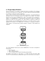
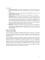
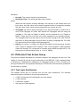
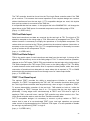
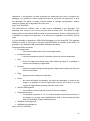
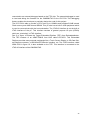
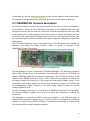
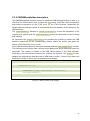
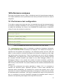
Figure 1 gives an overview over the basic project configuration. The Host illustrates the
workstation where the development tools for the Target µC are installed. The interface
between the Host and the CMARMJTAG is USB. This interface will be explained in
chapter 4. The CMARMJTAG is a state-of-the-art microcontroller which is the gateway
between the USB and JTAG interface. The JTAG interface is required to transfer the
debug information from the CMARMJTAG to the Target µC. The JTAG* interface is not the
standard JTAG interface of the CMARMJTAG. This interface is necessary to simulate a
JTAG interface. In this thesis three possible methods to simulate a JTAG interface are
explained.
Host
USB
4
USB
CMARMJTAG
JTAG*
6
JTAG
Target µC
Figure 1: Basic project configuration
The JTAG Debugger should have the name CMARMJTAG. This name is composed of
three phrases.
•
CM Cortex-M
•
ARM ARM Architecture
• JTAG Interface which is used for the debug communication
The applied microcontroller for this project is an ARM Cortex-M3 from NXP called
LPC1768. The used architecture (ARM) and the type of the microcontroller (Cortex-M) can
7
be found in the abbreviation of the JTAG Debugger. Also the interface which is used
between the CMARMJTAG and the target µC (JTAG) can be found in the abbreviation.
The JTAG Debugger should:
•
be able to integrate into OpenOCD (Open On-Chip-Debugger); OpenOCD is
explained in chapter 5
•
support ARM-JTAG interface communication
•
support variable JTAG speeds
•
support real-time debugging
•
support in-system programming
•
support boundary-scan testing
•
support all microcontrollers which are supported into OpenOCD
•
use a microcontroller which is:
o available
o low-cost
o and a state-of-the-art microcontroller
For this project the following features are no design goals:
•
displaying and storing of Embedded Trace information
•
Power Debugging founded by IAR Systems
•
a USB/Serial interface
•
a SWD interface communication
8
3 Examples of µC-based debugger
There are projects which are dealing with the development of µC-based debugger. This
chapter gives an overview of the related projects.
The SEGGER J-Link [cmp. to p. 24, SEGUM] is a USB powered JTAG emulator which
supports a large number of ARM cores. J-Link is based on a 32-bit RISC CPU and is used
for development and production purposes. It connects via USB to a PC running Microsoft
Windows 2000 or later. J-Link has a built-in 20-pin JTAG connector, which is compatible
with the standard 20-pin connector defined by ARM.
The RLink from Raisonance 11 [cmp. to p. 3, RLINK09] is a microcontroller debugger and
programmer which supports a range of target interfaces (JTAG, SWD, SWIM, ICC) and
connects to 32-bit and 8-bit µCs to program the target device and debug application in
real-time. The standard RLink consists of a ST7365xARxT1 µC. This chip is based on an
ARM7 core and used in the STM32 Primer1/2 of Raisonance. On the STM Primer1, JTAG
is used to program and debug the STM32 and on STM32 Primer2 SWD (Serial Wire
Debug) is used.
USBprog 12 [cmp. to USBJTAG07] is a free programming adapter. The adapter is based on
an ATmega32 and can be used for programming and debugging AVR and ARM cores, as
USB to RS232 converter, as JTAG interface or as simple I/O interface. The adapter allows
real-time debugging, setting breakpoints and single stepping.
eStick-JTAG 13 [cmp. to ESJTAG08] is a USB to JTAG adapter to program ARM-based
microcontrollers. This adapter allows real-time debugging, in-system programming and
boundary-scan testing for embedded targets. This adapter is based on the AT91USB162
of Atmel and was developed at the UAS Technikum Wien.
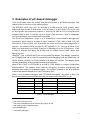
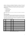
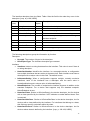
Table 1 lists µC-based debuggers and FTDI-based debuggers, the prices of them, the
theoretical download speed and whether they are supported by OpenOCD or not.
Name
Price[€]
Download speed
OpenOCD-Support
Segger J-Link*
248.00
12 Mibit/s
Yes
USBJTAG*
44.00
960 kibit/s
Yes
USBprog*
34.00
4,8 kibit/s
Yes
JTAGKey-Tiny**
29.00
6 Mibit/s
Yes
eStick JTAG*
15.00
70,4 kibit/s
Yes
Table 1: JTAG Debugger
11
http://www.raisonance.com/
12
http://www.embedded-projects.net/index.php?page_id=135
13
http://code.google.com/p/estick-jtag/
* µC-based debugger
** FTDI-based debugger
9
USBJTAG is a Windows based EJTAG tool for all MIPS core CPUs. It is possible to read
and write the memory and program the flash of these CPUs. The USBJTAG is supported
by OpenOCD. [cmp. to EJTAG11]
The Segger J-Link is the fastest debugger and offers many features and is supported in
OpenOCD. The USBprog is cheaper than the USBJTAG but does not achieve the
download rate. It is also supported by OpenOCD. The JTAGKey Tiny provided by Amontec
is the most efficient debugger. This debugger is based on the FTDI-Chip and is much
faster than the mentioned µC-based debugger at approximately the same price. The
eStick-JTAG as already explained is a very low-cost µC-based debugger and achieves a
considerable download speed. This debugger is not supported by OpenOCD by default. It
is possible to patch OpenOCD with an available patch file to integrate this debugger into
OpenOCD. The CMARMJTAG should gain the download speed of the JTAGKey Tiny but
with some modifications. After the reset the ARM CPU operates at a core frequency of 4
MHz provided by the internal oscillator. If the CPU runs with the internal oscillator the
maximum achievable JTAG clock is 2 MHz. The theoretical download speed mentioned in
table 1 is not possible at this configuration. Due to that fact the performance comparison is
done with the mentioned configuration.
10
4 Selected Topics of the utilized interfaces
After the analyses of the state-of-the-art debuggers it is necessary to focus on the most
important interfaces which are used in this thesis. This chapter focuses on the utilized
interfaces. On the one hand the USB interface is required to connect the CMARMJTAG to
the Host and on the other hand JTAG is required to transfer data between the target
microcontroller and the CMARMJTAG.
USB in a nutshell
USB is a handy solution if a computer is used to communicate with a device outside of a
computer. The interface is suitable for mass-produced, standard peripheral types as well
as small-volume designs, including one-of-a-kind projects. Additionally many
microcontrollers based on ARM provide a USB controller. USB offers some benefits for
both the users and the developers.
Benefits for Users:
•
Ease of Use
•
Automatic configuration
o The appropriate software driver is loaded automatically. Otherwise the OS
asks for the driver and automatically installs it.
•
Easy to connect
o Typical computers have USB ports built in where the external device can be
connected easily.
•
Easy cables
o USB connectors are small and compact in contrast to typical RS-232 and
parallel connectors.
•
Hot pluggable
o The USB device can be connected at any time without damaging the host
system
•
No power-supply required (sometimes)
11
Benefits for Developers
•
Versatility
o USB’s four transfer types and three speeds make the interface feasible for
many types of peripherals.
•
Operating System Support
o The OS (Operating System) automatically detects if a device is attached and
removed from a system
o The OS is able to communicate with newly attached devices to find out how
to exchange data with them.
o The OS provides a mechanism that enables software drivers to
communicate with the computer’s USB hardware and the applications that
want to access USB peripherals
•
Peripheral support
o Every USB peripheral must have a (may be built-in) controller chip that
manages the details of USB communications. Some of them are complete
microcontrollers or the USB controller is connected externally.
[cmp. p. 2-9, USBC]
IEEE Std. 1149.1 in a nutshell
The test logic, the Test Access Port (TAP) and the signals of JTAG are explained in
chapter 4.2. The IEEE14 Std. 1149.1 standard defines test logic that can be an integrated
circuit to provide standardized approaches to test the interconnect between integrated
circuits once they have been assembled onto a printed circuit board or other substrate, to
test the integrated circuit itself, and to observe or modify circuit activity during the
component’s normal operation.
The test logic consists of a boundary-scan register and other building blocks and is
accessed through a Test Access Port (TAP). [cmp. to p1, IEEE1149.1]
4.1 USB-Universal Serial Bus
As explained the CMARMJTAG uses two interfaces which are necessary to communicate
on the one hand with OpenOCD and on the other hand with the target hardware. One of
the interfaces is USB which is used to connect to OpenOCD. OpenOCD is used to emulate
the states & functionalities of the debug module of the target hardware on the host
machine. This software is described later. This chapter focuses on the descriptor types and
does not explain basic transactions and functionalities of the USB interface.
To be able to communicate via USB with the host machine it is necessary to configure the
USB-Device. Therefore a device descriptor data structure is used. All USB devices
14
http://www.ieee.org/index.html
12
respond to requests for the standard USB descriptors. The device must store the
information in the descriptors and respond to requests for the descriptors. To be able to
understand how the CMARMJTAG is configured and is registered on the host machine it is
necessary to explain the required types of descriptors and the configuration possibilities.
USB-Descriptors:
•
Device Descriptor
•
Configuration Descriptor
•
Interface Descriptor
•
Endpoint Descriptor
• String Descriptor
The descriptors types which are used in the main-file of the firmware are described in
detail.
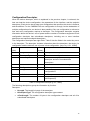
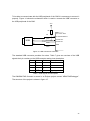
Device Descriptor
The device descriptor contains basic information about the device. The host first reads the
device descriptor when the device is attached. This descriptor provides information which
the host needs to retrieve additional information from the device. The device descriptor has
14 fields. Table 1 lists the fields in the order they occur in the descriptor. The descriptor
includes information about the descriptor, the device, its configuration and any classes the
device belongs to. [cmp. to p.96, USBC]
Offset
(dec)
Field
Size
(bytes)
Description
0
bLength
1
Descriptor size in bytes
1
bDescriptorType
1
The constant device
2
bcdUSB
2
USB Specification release number
4
bDeviceClass
1
Class code
5
bDeviceSubClass
1
Subclass code
6
bDeviceProtocol
1
Protocol code
7
bMaxPacketSize0
1
Max. packet size for endpoints
8
idVendor
2
Vendor ID
10
idProduct
2
Product ID
12
bcdDevice
2
Device release number
14
iManufacturer
1
Index of string descriptor for the manufacturer
15
iProduct
1
Index of string descriptor for the manufacturer
16
iSerialNumber
1
Index of string descriptor containing the serNum
17
bNumConfiguration
1
Number of possible configurations
Table 2: Device Descriptor [p.97, USBC]
13
The following descriptions group the information by function.
Descriptor:
•
bLength: The length in bytes of the descriptor
• bDescriptorType: The device descriptor type constant
Device:
•
bcdUSB: The USB specification that the device and its descriptors comply with in
BCD (binary-coded decimal) format.
•
idVendor: Vendor ID which could be used from the device driver to identify the
device.
•
idProduct: The product ID identifies the device. Each product ID is specific to a
vendor ID, so multiple vendors can use the same product ID without conflict.
•
iManufacturer: An index that points to a string describing the manufacturer. This
value is zero if there is no manufacturer.
•
iProduct: An index that points to a string describing the product. This value is zero
if there is no string descriptor.
•
iSerialNumber: An index that points to a string containing the device’s serial
number. This value is zero if there is no serial number. Some device classes (such
as mass storage) require serial numbers. Serial numbers are useful if users may
have more than one identical device on the bus and the host needs to keep track of
which is which even after rebooting.
Configuration:
•
bNumConfiguration: The number of configurations the device supports.
•
bMaxPacketSize0: The maximum packet size for the standard endpoints. The host
uses this information in the requests that follow.
•
bDeviceClass: For devices whose function is defined at the device level, this field
specifies the device’s class. Values from 0x01 to 0xFE are reserved for USB’s
defined classes. The value 0x00 means that the interface descriptor names the
class.
•
bDeviceSubclass: This field can specify a subclass within a class. If bDeviceClass
is 0, the bDeviceSubClass must be 0.
•
bDeviceProtocol: This field can specify a protocol defined by the selected class or
subclass.
[cmp. p. 96-101, USBC]
14
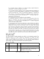
Configuration Descriptor
When the device descriptor, which is explained in the previous chapter, is retrieved, the
host can load the device configuration, the parameters for the interface, and the endpoint
descriptors. Each device has at least one configuration that specifies the device’s features
and the abilities. For the CMARMJTAG one configuration is enough, but the declaration of
multiple configurations for one device is also possible. Only one configuration is active at a
time and every configuration requires a descriptor. The configuration descriptor contains
information about the device’s use of power and the number of interfaces supported. Each
configuration descriptor has subordinate descriptors, including one or more interface
descriptors and optional endpoint descriptors.
The configuration descriptor has eight fields. Table 2 lists the fields in the order they occur
in the descriptor. The descriptor includes information about the descriptor, the device, its
configuration and the device’s use of power in that configuration. [cmp. to p. 101, USBC]
Offset
(dec)
Field
Size
(bytes)
Description
0
bLength
1
Descriptor size in bytes
1
bDescriptorType
1
The constant configuration
2
wTotalLength
2
The number of bytes in the configuration
descriptor and all of its subordinate
descriptors
4
bNumInterfaces
1
Number of interfaces in the configuration
5
bConfigurationValue
1
ID for requests
6
iConfiguration
1
Index of string descriptor for the
configurations
7
bmAttributes
1
Self/bus power and remote wakeup settings
8
bMaxPower
1
Bus power required, expressed as (maximum
miliamperes/2)
Table 3: Configuration Descriptor [p.101, USBC]
The following descriptions group the information by function.
Descriptor:
•
bLength: The length (in bytes) of the descriptor.
•
bDescriptorType: The configuration descriptor type constant
•
wTotalLength: The number of bytes in the configuration descriptor and all of its
subordinate descriptors.
15
Configuration:
•
bConfigurationValue: Indentifies the configuration for the requests. Must be 1 or
higher. A request with a value of zero causes the device to enter the not configured
state.
•
iConfiguration: Index to a string that describes the configuration. This value is zero
if there is no string descriptor.
•
bNumInterfaces: The number of interfaces in the configuration. The minimum is 1.
•
bmAttributes: Bit 0=1 if the device is self-powered or 0 if bus-powered. Bit 5=1 if
the device supports the remote wakeup feature, which enables a suspended USB
device to tell its host that the device wants to communicate. A USB device must
enter the Suspend state if there has been no bus activity for 3 milliseconds. If an
event at a suspended device requires action from the host, a device with remote
wakeup enabled can request the host to resume communications. The other bits in
the field are unused. Bits 0 through 4 must be 0. Bit 7 must be 1.
•
bMaxPower: Specifies how much bus current a device requires. The bMaxPower
value equals one half the numbers of milliamperes required. If the device requires
200 milliamperes, bMaxPower=100. The maximum current a device can request is
500 milliamperes.
[cmp. p. 101-103, USBC]
Interface Descriptor
After the configuration descriptor the interface descriptor has to be specified. The interface
descriptor provides information about a function or feature that a device implements. The
descriptor contains class, subclass, and protocol information and the number of endpoints
the interface uses.
In the configuration descriptor the number of interfaces is specified, which means that a
configuration can have multiple interfaces that are active at the same time. That is a big
difference between the configuration and interface descriptor. Only one configuration
descriptor can be active at a time, but multiple interfaces can be active at a time. Each
interface has its own interface descriptor and subordinate descriptor. Devices that uses
isochronous transfers, the transfer type is specified in the next chapter, must have
alternate interfaces because the default interface must request no isochronous transfer.
Changing interfaces is simpler then changing configurations.
16
The interface descriptor has nine fields. Table 4 lists the field in the order they occur in the
descriptor. [cmp. to p.108, USBC]
Offset
(dec)
Field
Size
(bytes)
Description
0
bLength
1
Descriptor size in bytes
1
bDescriptorType
1
The constant interface
2
bInterfaceNumber
1
Number identifying this interface
3
bAlternateSetting
1
Value used to select an alternate setting
4
bNumEndpoints
1
Number of endpoints supported, not counting
standard endpoint
5
bInterfaceClass
1
Class code
6
bInterfaceSubclass
1
Subclass code
7
bInterfaceProtocol
1
Protocol code
8
iInterface
1
Index of string descriptor for the interface
Table 4: Interface Descriptor [p.108, USBC]
The following descriptions group the information by function.
Descriptor:
•
bLength: The number of bytes in the descriptor.
•
bDescriptorType: The interface descriptor type constant
Interface:
•
iInterface: Index to a string that describes the interface. This value is zero if there is
no string descriptor.
•
bInterfaceNumber: Identifies the interface. In a composite device, a configuration
has multiple interfaces that are active at the same time. Each interface must have a
descriptor with a unique value in this field. The default is zero.
•
bAlternateSetting: When a configuration supports multiple, mutually exclusive
interfaces, each of the interfaces has a descriptor with the same value in
bInterfaceNumber and a unique value in bAlternateSetting.
•
bNumEndpoints: The number of endpoints the interface supports in addition to the
standard endpoints. For a device that supports only the standard endpoint,
bNumEndpoints is zero.
•
bInterfaceClass: Similar to bDeviceClass in the device descriptor, but for devices
with a class specified by the interface. 0xFF indicates a vendor-defined class. Zero
is reserved.
•
bInterfaceSubClass: Similar to bDeviceSubClass in the device descriptor, but for
devices with a class defined by the interface. For interfaces that belong to a class,
this field may specify a subclass within the class.
•
bInterfaceProtocol: Similar to bDeviceProtocol in the device descriptor, but for
devices whose class is defined by the interface. [cmp. p. 106-108, USBC]
17
Endpoint Descriptor
Every endpoint that is specified in an interface descriptor has an endpoint descriptor. The
standard endpoint never has a descriptor because every device must support the standard
endpoint, the device descriptor contains the maximum packet size, and the USB
specification defines everything else about the endpoint. Table 4 lists the endpoint
descriptor’s six fields in the order they occur in the descriptor. [cmp. to p 110, USBC]
Offset
(dec)
Field
Size
(bytes)
Description
0
bLength
1
Descriptor size in bytes
1
bDescriptorType
1
The constant endpoint
2
bEndpointAddress
1
Endpoint number and direction
3
bmAttributes
1
Transfer type supported
4
wMaxPacketSize
2
Maximum packet size supported
5
bInterval
1
Maximum latency/polling interval/NAK rate
Table 5: Endpoint Descriptor [p.110, USBC]
The following descriptions group the information by function.
Descriptor:
•
bLength: The number of bytes in the descriptor.
• bDescriptorType: The endpoint descriptor type constant
Endpoint:
•
bEndpointAddress: Contains the endpoint number and direction. Bits 0 through 3
are the endpoint number. Low-speed devices can have a maximum of 3 endpoints,
while full- and high-speed devices can have 16. Bit 7 is the direction: Out=0, In=1.
Bits 4, 5, and 6 are unused and must be zero.
•
bmAttributes: Bits 0 and 1 specify the type of transfer the endpoint support.
00=Control, 01=Isochronous; 10=Bulk, 11=Interrupt. For the standard endpoint,
control is assumed.
•
wMaxPacketSize: The maximum number of data bytes the endpoint can transfer in
a transaction. The allowed values vary with the device speed and type of transfer.
Bits 10 through 0 are the maximum packet size, from 0 to 1024 (0 to 1023 in
USB1.x). In USB 2.0, bits 12 and 11 indicate how many additional transactions per
microframe a high-speed endpoint supports: 00=no additional transactions,
01=additional, 10=2 additional, 11=reserved. In USB 1.x, these bits were reserved
and set to zero. Bits 13 through 15 are reserved and must be zero.
•
bInterval: Can indicate the maximum latency for polling interrupt endpoints, the
interval for polling isochronous endpoints, or the maximum NAK rate for high-speed
bulk OUT or control endpoints. The allowed range and how the value is used varies
with the device speed, the transfer type, and whether or not the device complies
with USB 2.0.
18
For low-speed interrupt endpoints, the maximum latency equals bInterval in
milliseconds. The value may range from 10 to 255.
For all full-speed interrupt endpoints and for full-speed isochronous endpoints on
1.x devices, the interval equals bInterval in milliseconds. For interrupt endpoints,
the value may range from 1 to 255. For isochronous endpoints in 1.x devices, the
value must be 1. For isochronous endpoints in full-speed 2.0 devices, values from 1
to 16 are allowed, and the interval is calculated as 2bInterval-1, allowing a range from 1
milliseconds to 32768 seconds.
For full-speed bulk and control transfers, the value is ignored.
For high-speed endpoints, the value is in units of 125 microseconds, which is the
width of a microframe. The value for interrupt and isochronous endpoints may
range from 1 to 16, and the interval is calculated as 2bInterval-1 to allow a range from
125 microseconds to 4096 seconds.
For high-speed bulk OUT and control endpoints, the value indicates the endpoint’s
maximum NAK rate. This value is relevant when the device has received data and
returned ACK, and the host has more data to send in the transfer. By returning
ACK, the device is saying that it expects to be able to accept the next transaction’s
data. If the next data packet arrives and for some reason the device can’t accept
the packet, the endpoint returns NAK. The bInterval value says that the endpoint
will return NAK no more than once in each period specified by bInterval. The value
can range from 0 to 255 microframes. A value of zero means that the endpoint will
never NAK. The host isn’t required to use the maximum-NAK-rate information.
[cmp. p. 108-112, USBC]
String Descriptor
The string descriptor contains descriptive text which is not necessarily required. The
descriptive strings can be used to describe the manufacturer, the product, the serial
number, the configuration and the interface. Class- and vendor-specific descriptors can
contain indexes to additional string descriptors. The string descriptor defines indexes to
various strings. Table 5 shows the descriptor’s fields and their purposes.
[cmp. to p.112, USBC]
Offset
(dec)
Field
Size
(bytes)
Description
0
bLength
1
Descriptor size in bytes
1
bDescriptorType
1
The constant string
2
bString or wLangID
Varies
For string descriptor 0, an array of 1 or more
Language Identifier codes. For other string
descriptors, a Unicode string.
Table 6: String Descriptor [p.113, USBC]
19
Descriptor:
•
bLength: The number of bytes in the descriptor.
• bDescriptorType: The string descriptor type constant
String:
When the host requires a String descriptor, the low-byte of the wValue field is an
index value. An index value of zero has the special function of requesting language
Ids, while other index values request strings that may contain any text.
•
wLangID[0...n]: Used in string descriptor 0 only. String descriptor 0 contains one or
more 16-bit language ID codes that indicate the languages that the string are
available in. The code for English is 0009h, and the subcode for U.S. English is
0004h. These are likely to be the only codes supported by an operating system.
The wLangID value must be valid for any of the other strings to be valid. Devices
that return no string descriptors must not return an array of language IDs. The USBIF’s web site has a list of defined USB language IDs.
•
bString: For values 1 or higher, the String field contains a Unicode string. Unicode
uses 16 bits to represent each character. With a few exceptions, ANSI character
codes 00h through 7Fh correspond to Unicode values 0000h through 007Fh. The
strings are not null-terminated. [cmp. p. 112-113, USBC]
4.2 JTAG-Joint Test Action Group
The previous chapter described the connection between the debugger and the host. This
chapter is intended to provide enough information of the IEEE Std. 1149.1 standard which
is necessary to understand the operations of a debugger based on JTAG. Therefore, the
test logic architecture, the signals provided by the TAP and the interconnection possibilities
are necessary to explain.
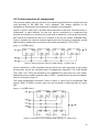
4.2.1 Test Logic Architecture
This chapter should give an overview over the test logic architecture. The following
elements should be included in the test logic architecture:
•
a TAP (Test Access Port) described in the next chapter
•
a TAP controller
•
a instruction register
•
and a group of data registers
20
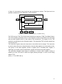
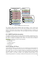
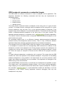
In figure 2 a conceptual view of the test logic architecture is shown. This figure can be a
possible embodiment of the IEEE Std. 1149.1 standard.
Test data register
Output
stage
TDI
TDO
Instruction register
Test Access Port (TAP) controller
TCK
TMS
TRST*
Figure 2: Test logic architecture [cmp. p.18, IEEE1149.1]
The TAP receives TCK (Test Clock) and interprets the signals on TMS (Test Mode Select).
The TAP controller generates clock or control signals or both as required for the instruction
and test data registers and for other parts of the architecture. The signals for the TAP
controller are described in the following chapter. The assembled TAP controller signals are
Test Access Port.
The instruction register allows the instruction to be shifted into the design. The instruction
is used to select the test to be performed or the test data register to be accessed or both.
The group of test data registers include a bypass and a boundary-scan register. It
optionally can include a device identification register and further test data registers.
The optionally included output stage is necessary to choose which register content is
shifted out at the TDO and to retime the signal passing through it to occur at the falling
edge of TCK.
[cmp. p. 17-18, IEEE1149.1]
21
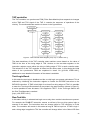
TAP controller
The TAP controller is a synchronous FSM (Finite State Machine) that responds to changes
at the TMS and TCK signal of the TAP. It controls the sequence of operations of the
circuitry. The mentioned state machine is shown in the figure below.
Figure 3: TAP controller state diagram [cmp. to p.19, IEEE1149.1]
The state transitions of the TAP controller state machine occurs based on the value of
TMS at the time of the rising edge of TCK. Actions on the test data registers or the
instruction register occurs either the rising or falling edge of TCK in each controller state.
The behaviour of the TAP controller is based on the active state. In this thesis the initial
states of the synchronous FSM are explained in detail. On [p.20-24, IEEE1149.1],
additional or more detailed information of the states is available.
Test-Logic-Reset
In this state the test logic is disabled and the on-chip logic can operate unhindered. This is
achieved by initializing the instruction register to contain the IDCODE instruction or the
BYPASS instruction. If TMS is held high for at least five rising edges of TCK it is possible
to enter the Test-Logic-Reset state from any state in the state machine (shown in figure 3).
It is also possible to enter this state, if 0 is applied to TRST*. If the Test-Logic-State is left
the Run-Test/Idle state is reached.
[cmp. p.20, IEEE1149.1]
Run-Test/Idle
In this state, activity in selected test logic occurs only when certain instructions are present.
For example the RUNBIST instruction causes a self-test of the on-chip system logic to
execute in this state. The instruction does not change while he TAP controller is in this
state. The controller will remain in this state as long as TMS is kept low. If TMS is logic 1
and a rising edge is applied to TCK the controller will change either in the Select-DR-Scan
22
state if one rising edge occurs or in the Select-IR-Scan state if two rising edges on TCK
occur. [cmp. p. 20, IEEE1149.1]
4.2.2 Test Access Port (TAP)
The Test Access Port is a general-purpose port that can provide access to many test
support functions built into a component. The TAP provides a minimum of three input
connections and one output connection. An optional fourth input connection provides for
asynchronous initialization of the test logic. This chapter focuses on the mentioned I/O
signals and their functionality. [cmp. p. 9, IEEE1149.1]
The TAP includes the following signals:
•
TCK-Test Clock Input
•
TMS-Test Mode Select Input
•
TDI-Test Data Input
•
TDO-Test Data Output
•
TRST*-Test Reset Input (optional)
o If the TAP controller is not reset at power-up automatically, a TRST* input
should be provided
The following paragraphs should explain the signals in detail.
TCK-Test Clock Input
This input is required to be able to use the serial test data path between the components
independently of the component-specific system clocks. It also permits shifting of test data
concurrently with normal system operation of the component. An independent clock
ensures that test data can be moved to or from a chip without changing the state of the onchip system logic. The independent clock is also important if the boundary-scan registers
should be usable for board interconnect testing.
The test clock should be a free-running clock with a 50% duty-cycle which can be stopped
in some situations for a period. The JTAG standard requires that the TCK can be stopped
at 0 indefinitely without causing any change to the state of the test logic. Due to the
stopped clock it is necessary that the connected devices retain their state so that the test
logic may continue when the clock operation restarts.
The test logic performs their operations at the rising or falling edge of the test clock. This
operations have to be completed within a fixed (frequency independent) delay after the
occurrence of the relevant change of the TCK. This delay has o be specified by the
component supplier.
[cmp p.10-11, IEEE1149.1]
TMS-Test Mode Select Input
The signal received at TMS is decoded by the TAP controller to control operations. The
signal at the TMS is sampled at the rising edge of the test clock. The load at TMS should
be as small as possible.
23
The TAP controller should be forced into the Test-Logic-Reset controller state if the TMS
pin is undriven. This ensures that normal operation of the complete design can continue
without interference from the test logic. If TTL-compatible designs are used, this implies
that a pull-up resistor is connected to the TMS line.
It is expected that the bus master - in this project this is the CMARMJTAG - will change the
signal driven to the TMS inputs of connected components on the falling edge of TCK.
[cmp p. 11, IEEE1149.1]
TDI-Test Data Input
Serial test instructions and data are received by the test logic at TDI. The signal at TDI
should be sampled on the rising edge of TCK. Data which is propagated from TDI to TDO
without inversion is necessary to simplify the operations of a compatible component. The
values which are received at the TDI are clocked into the selected registers (instruction or
test data) on the rising edge of TCK. For TTL-compatible designs it is necessary to connect
a pull-up resistor on the components TDI pin.
[cmp. p. 12, IEEE1149.1]
TDO-Test Data Output
TDO is the serial output for test instructions and data from the test logic. A change of the
signal at TDO should only occur at the falling edge of TCK. To ensure race-free operation,
changes on the TAP inputs (TMS & TDI) are clocked into the test logic at the rising edge of
TCK while changes at the TAP output (TDO) occur on the falling edge of TCK. The ability
to switch between active and inactive drive is required to allow parallel, rather than serial,
connection of board-level test data paths in cases where this is required. In TTL or CMOS
technologies this requirement can be met through use of a 3-state output buffer.
[cmp. p. 12, IEEE1149.1]
TRST*-Test Reset Input
The optional TRST* provides the ability to asynchronous initialize or reset the TAP
controller. If a TRST* is supported by the TAP, the TAP controller should be able to enter
the Test-Logic-Reset controller state asynchronously, when a logic 0 is applied to TRST*.
To ensure deterministic operation of the test logic, TMS should be held at 1 while the
signal applied at TRST* changes from 0 to 1 to ensure that the test logic responds
predictably. If rising edges occur simultaneously at TRST* and TCK when a logic 0 is
applied to TMS, a race will occur, and the TAP controller may either remain in the TestLogic-Reset controller state or enter the Run-Test/Idle controller state.
For TTL-compatible designs it is necessary to connect a pull-up resistor to TRST* to
ensure that in case of a non-terminated TRST* input, test logic operation can proceed
under control of signals applied at the TMS and TCK inputs. It is also possible to disable
the test logic by hard-wiring TRST* to logic 0.
[cmp. p. 13, IEEE1149.1]
24
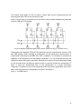
4.2.3 Interconnection of components
The previous chapter gave an overview of the signals and defined their requirements and
rules according to the IEEE Std. 1149.1 standard. This chapter specifies on the
possibilities to interconnect the components compatible to this standard.
Figure 4, figure 5 and figure 6 illustrate three alternative board level interconnections of
components. In each example, the test bus can be controlled by a component that
provides an interface to a test bus at the next level of assembly. In this project the device
that controls the board-level test bus is referred to as the bus master (CMARMJTAG).
Figure 4 contains the minimum required signals which are necessary to assemble a serial
path formed by a daisy-chain connection of the serial test data pins (TDI & TDO).
[cmp. p. 14, IEEE1149.1]
Figure 4: Serial connection using one TMS signal [p. 14, IEEE1149.1]
Figure 4 shows four JTAG-compatible devices which are serial connected. In this project
the bus slave can be any controller which is supported by OpenOCD. The JTAG signals
(TDI, TMS, TCK, TDO) are provided by the CMARMJTAG which acts as a bus master.
Additionally the bus master optionally offers a TRST*, as described in the previous chapter,
which is not shown in figure 4.
The hybrid serial/parallel connection, shown in figure 5, uses a pair of coordinated TMS
signals (TMS1 & TMS2) to ensure that only one serial path is scanning data at a given
time.
[cmp. p. 14, IEEE1149.1]
Figure 5: Connection in two paralleled serial chains [p. 14, IEEE1149.1]
25
The 3-state output buffer of TDO is used to ensure that only the components that are
scanning data have TDO in the active drive state.
Figure 5 shows how to interconnect four bus slaves using multiple independent paths with
common TMS and TCK signals.
Figure 6: Multiple independent paths with common TMS & TCK sig. [p. 15, IEEE1149.1]
These paths have separate TDI and TDO signals but can be controlled from common TCK
and TMS signals. When choosing a configuration for the board-level interconnection of
components conforming to the IEEE Std. 1149.1 standard, it is necessary to consider the
capability of test equipment and test pattern generators. It is fully expected that any test
equipment and/or test pattern generators that intends to support a test methodology based
on the boundary-scan architecture would be able to test the board-level configuration of
figure 4, since the degenerated form of this configuration is a single conformant
component. Furthermore, some test equipment and/or test pattern generators may not be
able to test the board-level configurations of figure 5 and figure 6.
[cmp. p. 14, IEEE1149.1]
26
5 OpenOCD-Open On-Chip-Debugger in a nutshell
The previous chapters described the interfaces which are used in this project. This chapter
explains the program running on the host, shown in figure 1, which uses the USB interface.
This chapter gives a basic overview on OpenOCD and is not intended to explain the
details. In [3] OpenOCD is explained in detail. Figure 7 shows the host configuration which
is used in this project.
Host
OpenOCD
USB
Figure 7: Host configuration
OpenOCD runs as a daemon process on the host workstation, making use of a JTAG
compliant hardware interface that connects to the target system.[cmp. p.32, OOCD05]
This process provides two USB endpoints. One endpoint is configured for input
communication and the other endpoint controls the output communication. The endpoints
are connected to the USB peripheral of the CMARMJTAG which converts the USB
commands provided by OpenOCD into commands which are transferred to the JTAG
interface of the target system. The CMARMJTAG also converts the JTAG responds of the
target system into USB commands readable for OpenOCD.
OpenOCD is able to load the code in the target memory, to control code execution on the
target and examine the target state. [cmp. p. 32, OOCD05]
If there is no code on the target it is necessary to perform initial steps to be able to load the
code in the target memory. OpenOCD provides commands to set up the configuration of
the target to be able to transfer the compiled code. OpenOCD supports many different
flash devices and enables the user to add devices.
Supported Flash devices:
•
AT91SAMxxxx from ATMEL
•
i.MXxx from Freescale
•
LM3Sxxxx from LuminaryMicro
•
LPCxxxx from NXP
•
OMAPxxxx from Texas Instruments
•
S3Cxxxx from Samsung
• STxxxx from STMicroelectronics
OpenOCD offers a possibility to integrate additional JTAG hardware interfaces like the
CMARMJTAG and it is possible to change the amount of the debug information during
runtime to allow a developer to examine the debugger’s behaviour during selected
27
operations. A configuration file and command line arguments are used to configure the
debugger. It is possible to select configuration files via command line arguments, to give
the developer the ability to debug multiple targets or multiple configurations, without
change or replace the configuration file every time.
[cmp. p.32, OOCD05]
The command line interface uses a telnet server embedded in the debugger. The
developer can connect to the server process using a telnet client. This allows a single
debug system to be used by different users at remote locations. Via the configuration file it
is possible to configure the telnet port. If no telnet port is specified, port number 4444 is
used.
It is also possible to determine a GDB (GNU Debugger) port for OpenOCD. The standard
GDB port number is 3333. Due to this port OpenOCD offers an interface to the GDB. It is
possible to use standard GDB commands to configure the target.
Supported GDB commands:
•
Poll target state
o retrieves information about the current target states.
•
Architecture state
o retrieves architecture specific information about the current target state
•
Halt
o forces the target into debug state; after halting the target it is possible to
examine and modify the target state
•
Resume
o makes the target leaving the debug state; target starts executing at the point
where it was halted
•
Step
o target executes exactly one instruction
•
Reset
o this resets all system functionality, but leaves the debugger in control of the
target; it is possible to halt the target after coming out of reset; if no halt
occurs the target starts executing from the reset vector
•
Set/Get GDB registers
o it is possible to set and get the content of the core registers
•
Read/Write memory
o it is possible to perform 8-, 16-, or 32-bit accesses to the internal memory of
the target; e.g. monitor mwb 0xXXXXXXXX 0x00 this command means
Memory Write Byte [Target Address] [Value]
•
Add/Remove breakpoints
• Add/Remove watchpoints
[cmp. p.34-35, OOCD05]
28
OpenOCD supports four different levels of debug information.
•
Error messages which are fatal for the program’s further execution. Code in
OpenOCD LOG_ERROR
•
Warnings that indicate a problem, but allow the program to continue execution.
Code in OpenOCD LOG_WARNING
•
Informational messages that are generated during normal program execution.
These messages give the user additional information about the debuggers
operation. Code in OpenOCD LOG_INFO
•
Debug messages, which may occur at a high rate. These messages are used to
identify problems during further development of the debugger. Code in OpenOCD
LOG_DEBUG
[cmp. p. 38, OOCD05]
In the following chapters there are many topics dealing with OpenOCD. Therefore, this
chapter highlighted basic functionalities and features.
29
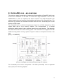
6 Cortex-M3 core - an overview
The previous chapter focused on the features and functionalities of OpenOCD which runs
on the host workstation. To be able to connect the target hardware to the PC the
CMARMJTAG is used. As explained, this device consists of an ARM Cortex-M3. This
chapter explains the most important functionalities and features of the Cortex-M3 core. The
document [4] provides more detailed information about the core functionality and is used
as basis of this chapter.
The Cortex-M3 core is a 32-bit microprocessor which has a 32-bit data-path, a 32-bit
register bank and a 32-bit memory interface. This microprocessor is a Harvard
architecture, which means it has a separate instruction bus and data bus. The instruction
and data buses share the same memory space. The Cortex-M3 core supports both little
endian and big endian memory systems. Figure 8 shows a conceptual overview of the
core.
[cmp. p. 13, GCM307]
Figure 8: A conceptual view of the Cortex-M3 core [p. 14, GCM307]
The functionality of the built-in components of the CM3 (Cortex-M3) core are explained
step by step in the following chapters.
30
Core Registers
The CM3 processor has the core registers R0-R15. R0-R12 are general purpose registers
for data-operations. The CM3 core contains two stack pointers, R13. These two pointers
are banked which implies that only one is visible at a time. The MSP (main Stack Pointer)
is the default stack pointer and is used by the OS kernel and the exception handlers. The
PSP (Process Stack Pointer) is used for user application code. If a subroutine is called the
return address is stored in the link register R14. The program counter is stored in R15.
Some special registers are also available in the CM3 core. The xPSR register contains the
ALU flags, e.g. zero flag, carry flag, execution status etc. The PRIMASK register enables
the developer to disable all interrupts expect the NMI (non-maskable interrupt) and
HardFault. The FAULTMASK register is used to disable all interrupts expect NMI. The
BASEPRI register is used to disable all interrupts of specific priority level or lower priority
level. The CONTROL register defines the privileged status and stack pointer selection.
[cmp. p. 15-16, GCM307]
Operation Modes
The CM3 core has two operation modes and two privilege level. If the processor comes out
of reset it is in Thread Mode, with privileged access rights. In the privileged state a program
has access to all memory ranges. If the CM3 core runs at privileged access level it is
possible to write to the control register to switch the mode. If an exception is thrown the
processor switches into privileged access level and returns back to the previous access
level after execution of the exception. To be able to adjust the control register it is
necessary for a user program to go through an exception to program this register. This
separation of the access levels is necessary to improve systems reliability and to prevent
system configuration registers from being accessed or changed by some untrusted
programs.
[cmp. p. 16-17, GCM307]
NVIC-Nested Vectored Interrupt Controller
The NVIC is closely coupled to the CM3 core and provides a number of features which are
explained in this section.
[cmp. p.17, GCM307]
Nested Interrupt Support
It is possible to define different interrupt priority levels to the external interrupts and to most
internal system exceptions. The NVIC compares the priority of the occurred interrupt to the
currently running priority level. If the occurred interrupt has a higher priority than the
currently running interrupt the processor will override the current running task.
[cmp. p.17, GCM307]
31
Vectored Interrupt Support
The starting addresses of the interrupt service routines (ISR) are located in the vector table
in the memory. There is no need to use software to determine and branch to the starting
address of the ISR which means that it takes less time to process an interrupt request.
[cmp. p.17, GCM307]
Dynamic Priority Changes Support
The priority levels of interrupts can be changed by software during execution. Interrupts
which are defined are blocked from activation until the ISR is completed. There is no risk of
accidental re-entry.
[cmp. p.17, GCM307]
Reduction of Interrupt Latency
The CM3 core includes a number of features to lower the interrupt latency. These features
are including automatic saving and restoring some register contents, reducing delay from
switching from one ISR to another and handling late arrival interrupts.
[cmp. p.17, GCM307]
Interrupt Masking
It is possible to mask interrupts and system exceptions based on their priority level or using
the interrupt mask registers BASEPRI, PRIMASK, and FAULTMASK. This ensures that
time-critical tasks can be finished on time without being interrupted.
[cmp. p.17, GCM307]
The Memory Map
The CM3 has a predefined memory map which means that the built-in peripherals can be
accessed via simple memory access instructions. The memory map gives the CM3 the
ability to be optimized for speed and it is easier to integrate the core in system-on-a-chip
(SoC) designs. Figure 9 shows the 4GB memory space of the CM3 core.
[cmp. p.19, GCM307]
32
Figure 9: The CM3 Memory Map [p.19, GCM307]
The System Level memory space includes the private peripherals like the NVIC, the
Memory Protection Unit (MPU) registers and the debug components. The External Device
section includes the external peripherals and the External RAM section is used for external
memory. The SRAM section is used for internal static RAM and the Code section includes
the user program code and the exception vector after power-up. The System Level
memory region makes it easy to port applications between different CM3 products.
[cmp. p. 19, GCM307]
The Bus Interface
As shown in figure 8 the CM3 provides a code memory bus, which physically consists of
two buses. One bus is called I-Code (Instruction Bus) and the other is called D-Code (Data
Bus). This bus is optimized for best instruction execution speed. The system bus is used to
access memory and peripherals which provides access to the SRAM peripherals, external
RAM, external devices and a part of the System Level memory region. For example the
debugging components and the NVIC are accessed through the private peripheral bus.
[cmp. p. 20, GCM307]
The Memory Protection Unit-MPU
The MPU enables the developer to set up rules for privileged access and user program
access. If a rule is violated, a fault exception is generated and it is possible to analyze the
problem in the fault exception handler.
33
Commonly the MPU is used and set up by an operating system, which can define the rule
that the OS kernel is able to access privileged data and registers. The MPU can also be
used to make memory regions read-only, to prevent accidental erasing of data.
The MPU feature is optional and is determined during the implementation stage of the
microcontroller or SoC design.
[cmp. p. 20, GCM307]
Debugging Support
The debugging hardware of the CM3 is based on the CoreSight architecture. Instead of the
built-in JTAG interface the CM3 includes a decoupled debug interface module and a bus
interface called Debug Access Port (DAP) on core level. The DAP enables external
debuggers to access control registers as well as system memory. The bus interface is
controlled by the Debug Port (DP) device. There are three integrable DP modules:
•
SWJ-DP
o Supports the JTAG protocol as well as the Serial Wire protocol
•
SW-DP
o Supports the Serial Wire protocol
•
JTAG-DP
o Supports the JTAG protocol
The manufacturer can also include an Embedded Trace Macrocell (ETM) which allows
instruction trace. This information is output via the Trace Port Interface Unit (TPIU) and the
host workstation can collect the executed instructions via an external trace-capturing
hardware.
[cmp p.24, GCM307]
34
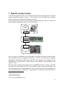
7 Specific project setup
The previous chapters focused on the theoretical basics of the essential parts of the basic
project configuration, shown in figure 1. The interfaces JTAG and USB where explained
and an overview of the CM3 core operations were given.
This chapter gives an overview of the specific project configuration. Figure 10 shows the
specific project configuration which is used in this project.
A
Host
OpenOCD
0.4.0
USB
4
B
USB
CMARMJTAG
JTAG-IO
6
C
ARM-JTAG
ARM7TDMI-S
TEP
Figure 10: Specific Project Configuration
Part A of figure 10 illustrates the host workstation, the OpenOCD and the USB interface.
The workstation (Host) is equipped with Ubuntu 15 10.4 LTS, a state-of-the-art Integrated
Development Environment (IDE) and OpenOCD 0.4.0 adapted and compiled for the
CMARMJTAG. As IDE, Eclipse 16 Galileo with the GNU ARM and Zylin Embedded CDT
plug-ins is used.
Part B of figure 10 shows the prototype of the CMARMJTAG which consists of an ARM
Cortex-M3 from NXP called LPC1768. This evaluation board initially was designed to fit
onto the baseboard from EmbeddedArtists 17 which provides many external peripherals for
microcontrollers based on ARM cores. Additionally the JTAG pins of the LPC1768 are
15
16
17
http://ubuntuusers.de/
http://www.eclipse.org/
http://www.embeddedartists.com/
35
connected to an external debugger based on the FTDI chip. The external debugger is used
to load and debug the firmware for the CMARMJTAG to the LPC1768. This debugging
feature enables the developer to precisely design the code for this project.
The LPC1768 is able to provide a CPU clock up to 100MHz and provides 512kB internal
Flash memory and 64kB internal SRAM. This µC also has a built-in USB peripheral which
is used to communicate with the host workstation. The JTAG-IO interface is not the built-in
JTAG interface of the µC. This interface consists of general purpose I/O pins (GPIOs)
which are “simulating” a JTAG interface.
Part C of figure 10 shows the Target Embedded Platform (TEP) from EmbeddedArtists.
The TEP consists of an ARM7TDMI-S from NXP called LPC2478. This Embedded
Platform provides many external peripherals like a Touch Screen Display, a SD-Card Slot,
an Ethernet connector, a USB Host/OTG/Device interface, etc. The JTAG interface, called
ARM-JTAG in figure 10, is also available on the TEP. This interface is connected to the
JTAG-IO interface of the CMARMJTAG.
36
8 Implementation
The previous chapter has given an overview of the specific project configuration. This
chapter explains the details of the implementation, describes how to integrate a new
interface into OpenOCD, explains the driver which handles the JTAG commands and
configures the USB device. Finally the USB firmware library is explained.
8.1 Integration of a new interface into OpenOCD
To be able to compile OpenOCD for the CMARMJTAG it is necessary to modify some files
in the standard OpenOCD source tree. This chapter describes how to integrate a new
interface into OpenOCD. The following files have to be edited to enable the interface for
compilation. The root (.) directory is openocd-0.4.0/.
a) ./configure.in
b) ./configure
c) ./config.h
d) ./README
e) ./doc/openocd.texi
f) ./src/Makefile.in
g) ./src/Makefile.am
h) ./src/jtag/interfaces.c
i) ./src/jtag/drivers/Makefile.in
j) ./src/jtag/drivers/Makefile.am
k) ./src/jtag/drivers/Makefile
Additionally it is necessary to add a driver file to implement the interface specific routines
and to add a basic configuration file for the interface. The interface driver has to be added
to ./src/jtag/drivers/. Currently the CMARMJTAG driver is included and named
cmarmjtag.c. The structure of the driver and the functionalities of the included routines
are explained in chapter 8.2. The interface configuration file has to be added to
./tcl/interface/. In this project there already exists a configuration file named
cmarmjtag.cfg. To ease the integration process of a new interface a patch file is used to
auto-integrate the new contents. This patch file is also available in the thesis folder.
37
8.2 OpenOCD driver description
The previous chapter described how to register a new interface into the standard
OpenOCD source tree. To be able to access the USB port on the host workstation where
the CMARMJTAG is connected and to execute and set up the proper JTAG commands
based on the JTAG state machine, it is necessary to develop a driver which provides these
functionalities. This chapter describes the structure of the CMARMJTAG driver and
explains the most important C-routines of it.
If the JTAG-Debugger is attached to the host, an initial registering procedure is performed.
During this procedure the host reads out the required information to locate and enable the
new USB device. The device descriptor on the CMARMJTAG provides this information. To
check whether the USB device is registered correctly it is necessary to execute the
lsusb –v | -less in the command shell. The following lines show the output for the
CMARMJTAG.
Bus 005 Device 008: ID ffff:0005
Device Descriptor:
bLength
18
bDescriptorType
1
bcdUSB
2.00
bDeviceClass
255 Vendor Specific Class
bDeviceSubClass
0
bDeviceProtocol
0
bMaxPacketSize0
64
idVendor
0xffff
idProduct
0x0005
bcdDevice
1.00
iManufacturer
1 FHTW
iProduct
2 CMARMJTAG
iSerial
3 0000:00:1
bNumConfigurations
1
Listing 1: Device Descriptor (console output)
38
Listing 1 shows the retrieved device descriptor. The vendor identification (VID) and product
identification (PID) is configured to 0xffff and 0x0005. These two parameters are necessary
to identify the USB device in the CMARMJTAG driver. The manufacturer string, the product
string and the serial string are configured via the descriptor in the CMARMJTAG firmware.
This device descriptor supports one configuration.
Configuration Descriptor:
bLength
9
bDescriptorType
2
wTotalLength
60
bNumInterfaces
1
bConfigurationValue
1
iConfiguration
0
bmAttributes
0x80
MaxPower
100mA
Listing 2: Configuration Descriptor (console output)
Listing 2 shows the configuration descriptor of the USB device on the external debugger.
The descriptor type field enables the host to identify this descriptor as the configuration
descriptor. This configuration descriptor supports one interface and the configuration index
is configured to 0. The attributes value indicates that the device is bus powered which
means that the host acts as the power supply for the USB device on the CMARMJTAG.
The configuration descriptor in the CMARMJTAG firmware configures the power field to
0x32 which means 100mA. For the current project configuration the provided current is
adequate. The maximum value for this field is 0xFA: This value is 250dec and configures
the USB device to 500mA.
Interface Descriptor:
bLength
bDescriptorType
bInterfaceNumber
bAlternateSetting
bNumEndpoints
bInterfaceClass
bInterfaceSubClass
bInterfaceProtocol
iInterface
9
4
0
0
2
255 Vendor Specific Class
0
0
0
Listing 3: Interface Descriptor (console output)
Listing 3 shows the interface descriptor of the CMARMJTAG USB device. This interface
supports no alternate setting and provides two endpoints which are configured in the
endpoint descriptor (Listing 4). The interface index is configured to 0.
39
Endpoint Descriptor:
bLength
7
bDescriptorType
5
bEndpointAddress
0x05
bmAttributes
2
Transfer Type
Synch Type
Usage Type
wMaxPacketSize
0x0168
bInterval
0
Endpoint Descriptor:
bLength
7
bDescriptorType
5
bEndpointAddress
0x82
bmAttributes
2
Transfer Type
Synch Type
Usage Type
wMaxPacketSize
0x0168
bInterval
0
EP 5 OUT
Bulk
None
Data
1x 360 bytes
EP 2 IN
Bulk
None
Data
1x 360 bytes
Listing 4: Input / Output Endpoint Descriptor (console output)
The endpoint descriptor, shown in Listing 4, is necessary to configure the required
endpoints of the USB device. The first endpoint is an out endpoint.
The communication direction is configured from the host point of view. This means via the
out endpoint on the host, data can be written to the CMARMJTAG. The out endpoint of the
USB device of the external debugger is configured to address 0x05. But the CMARMJTAG
receives data via this endpoint.
The read endpoint of the host receives data from the external debugger. But the read
endpoint of the CMARMJTAG sends data to the host. The out endpoint address is
configured to 0x05 and the transfer type is configured to bulk transfers. The out endpoint is
used to transfer data and has a maximum packet size of 360 bytes because during a
debugging session no more than 360 bytes are transmitted via the TDO pin.
The second endpoint is an in endpoint or read endpoint. This endpoint has the address
0x82. The read endpoint transfer type is configured to bulk transfer and is able to transfer a
maximum of 360 bytes in a packet. The packet length is the same length as the buffer size
of the external debugger.
Device Status:
(Bus Powered)
0x0000
Listing 5: Device Status (console output)
40
Listing 5 shows the device status. After attachment of the USB device and successful
registration the device status should be 0x0000. In the CMARMJTAG driver there are
some #defines which are necessary to provide parameters for the USB device on the
host and to determine the speed limits of the JTAG clock. The interface mapping between
the standard OpenOCD low-level functions is done via the interface structure shown in
Listing 6.
struct jtag_interface cmarmjtag_interface =
{
.name = "cmarmjtag",
.commands = cmarmjtag_command_handlers,
.execute_queue = cmarmjtag_execute_queue,
.speed = cmarmjtag_speed,
.speed_div = cmarmjtag_speed_div,
.khz = cmarmjtag_khz,
.init = cmarmjtag_init,
.quit = cmarmjtag_quit,
};
Listing 6: CMARMJTAG interface structure (code snippet)
This interface structure enables the developer to implement interface specific functions
accessible via OpenOCD. Figure 11 gives an overview of the CMARMJTAG driver
structure. The routines speed() and speed_div(), shown in Listing 6, are present in the
driver but not used. Thus these routines do not appear in figure 11.
JLink driver
struct jtag_interface jlink_interface =
{
...
};
USBprog driver
OpenOCD High-Level routines
OpenOCD main()
struct jtag_interface USBprog_interface =
{
...
};
OpenOCD init()
JTAG init()
CMARMJTAG driver
struct jtag_interface
{
char *name;
const struct command_registration *commands;
int (*execute_queue) (void);
int (*khz) (int khz);
int (*init) (void);
int (*quit) (void);
};
.
.
.
OpenOCD close()
struct jtag_interface cmarmjtag_interface =
{
.name = "cmarmjtag",
.commands = cmarmjtag_command_handlers,
.execute_queue = cmarmjtag_execute_queue,
.khz = cmarmjtag_khz,
.init = cmarmjtag_init,
.quit = cmarmjtag_quit,
};
OpenOCD Low-Level
routines
USB_Open()
USB_Bulk_Read()
USB_Bulk_Write()
.
.
.
USB_Close()
Other driver
struct jtag_interface other_interface =
{
...
};
Figure 11: CMARMJTAG Driver Overview
41
The principle structure of the driver is determined by the external interface routines shown
in Listing 6. The init routine opens the attached USB device. This routine initializes the
USB device of the host, loads the busses and the devices and locates the USB device due
to the VID and PID parameter, which are defined in the driver. The usb_open() routine
returns a structure which holds the configuration of the attached USB device. Via this
structure it is possible to communicate with the external debugger (USB device). After the
USB device configuration is set up a reset message is sent to the CMARMJTAG.
The cmarmjtag_reset() routine induces the CMARMJTAG to perform a reset
sequence via the TRST_N pin and the SRST_N pin. The reset function calls the
cmarmjtag_simple_command() routine which is used to send messages and receive
the reply with a command header. The low-level routines cmarmjtag_usb_write() and
cmarmjtag_usb_read()
are
necessary
to
send
the
data
provided
by
the
usb_out_buffer[] and usb_in_buffer[] array. Figure 12 shows the configuration of
one USB frame.
USB Data Packet
USB Frame
Sync
DLH
PID
DLL
CRC16
JTC
EOP
Payload
Figure 12: USB Frame configuration
The USB frame provides information about the payload length and the JTAG command
which has to be performed and the payload itself. The payload length is divided into two
bytes. The payload length can vary between 0 and 357 bytes. The first byte of the USB
frame, shown in figure 12, provides the high-byte of the payload length (DLH). The second
byte of this frame illustrates the low-byte of the USB frame. The third byte contains the
JTAG command which has to be performed. The following JTAG commands are possible:
•
JTAG_CMD_TAP_OUTPUT
0x1
o The payload contains the values which are set & reset the TDI, TMS pins
and the value for the single pin is extracted on the CMARMJTAG.
•
JTAG_CMD_SET_TRST
0x2
o Disable TAP Reset. Enable TAP.
•
JTAG_CMD_SET_SRST
0x3
o Disable software reset.
•
JTAG_CMD_READ_INPUT
0x4
o Read the data on the TDO pin.
•
JTAG_CMD_TAP_OUTPUT_EMU 0x5
o This command is not supported on the CMARMJTAG in this project.
•
JTAG_CMD_SET_DELAY
0x6
o Adjust the JTAG speed in kHz.
42
•
JTAG_CMD_SET_SRST_TRST
0x7
o Disable TAP Reset, enable TAP and disable software reset simultaneously
The amount of transmitted & received bytes are stored in a variable which is used to check
whether the transmission was successful or not. After the reset is performed the TAP is
initialized.
In the cmarmjtag_execute_queue() routine proper subroutines are provided to
implement different commands.
The cmarmjtag_runtest() routine performs a given amount of JTAG state steps, if the
JTAG state machine is not already in the idle state. Within this routine the TAP Buffer
routine cmarmjtag_tap_append_step() is called to perform the determined steps. The
cmarmjtag_end_state() function checks whether the JTAG state machine of the target
µC is in an valid end state or not.
The cmarmjtag_state_move() routine moves the JTAG state machine of the debugged
hardware to the next state that valid.
The cmarmjtag_path_move() routine performs a number of steps in a defined path of
the JTAG state machine.
The cmarmjtag_scan() routine scans the connected JTAG chain and performs the
required state transitions to complete the task.
The reset command during the execution of the queue controls the attached JTAG chain
and performs a reset afterwards.
The cmarmjtag_tap_execute() function prepares the values for the USB buffer. The
JTAG command JTAG_CMD_TAP_OUTPUT is signalling that the payload contains a new
TAP sequence. The answer on this payload is transmitted via USB to the host workstation
and is stored in the usb_in_buffer[]. At the end of the sequence the content of the
usb_in_buffer[] is copied to the tdo_buffer[] which stores the information for
further operations.
The jtag_sleep() routine is a member of the core routines, which means that this
function calls a core routine located in core.c.
The cmarmjtag_khz() routine is one of the members of the external interface routines.
This function checks whether the desired speed value is between the borders of the speed
limit and checks whether the value can be divided by 100 without a remainder. The
CMARMJTAG supports speeds from 100 kHz till 2000 kHz. These limits are defined at the
top of the driver file and shown in Listing 7.
#define CMARM_MAX_SPEED
#define CMARM_MIN_SPEED
2000
100
Listing 7: CMARMJTAG supported speed limits (code snippet)
The step size of the speed should be 100 kHz. If the speed is above the upper limit of the
speed, this routine sets the speed to the upper limit. If the speed is below the lower limit of
the supported speed, this routine sets the speed to the lower limit. If the desired speed is
43
not dividable by 100 the cmarmjtag_khz() routine sets the speed to next slower speed.
For example, if the desired speed is 1425 kHz, the driver sets the speed to 1400 kHz.
8.3 CMARMJTAG firmware description
The previous chapter focused on the implementation of the driver on the host workstation.
As described in chapter 8.2 the USB device peripheral on the CMARMJTAG has to be
configured correctly, that the host can retrieve the required information and set up a USB
communication. This chapter describes the firmware which is used in this project and runs
on the LPC1768. Additionally this chapter gives an overview of the firmware structure, lists
the used development tools and add-ons and explains important configuration parameters
and functions.
The FTDI-based debugger which is connected to the LPC1768 enables the developer to
download and debug the written firmware. Figure 13 shows a prototype of the
CMARMJATG used in this project.
Figure 13: Prototype of the CMARMJTAG
The red rectangle of figure 13 shows the FTDI-based debugger. This debugger provides a
(Mini-) USB interface to the host workstation. This debugger consists of a FT2232D, an
external EEPROM (M93C46) and passive components. The FT2232D provides a JTAG
interface and a RS232 interface for the µC. The FT2232D can be supplied via USB or via
the supply voltage of the target µC. In this project the USB supply voltage is used. To be
compatible to the voltage range of the µC pins it is necessary to supply the FT2232D with
the corresponding voltage. Therefore, if the USB supply voltage is used, an external
voltage regulator is used.
The blue rectangle shows the µC (in this project an ARM Cortex-M3 LPC1768 from NXP),
the external oscillator (12MHz) and the µC pins which are connected to external pin
connectors.
This debugger is connected via USB to the host workstation. If the USB connection is
established it is possible to access the µC via USB. At the host workstation the USB port
appears as a device named FHTW JTAGKey. This enables the developer to connect to the
µC via OpenOCD and start firmware developing.
44
To be able to communicate with the USB peripheral of the CM3 it is necessary to connect it
properly. Figure 14 shows the schematic which is used to connect the USB connector to
the USB peripheral of the CM3.
3V3
10k
LPC1768 – CM3
red
P1.30/VBUS/AD0.4
green
P0.29/U1D+
P0.30/U1D-
USB
white
GND
black
Figure 14: USB connection schematic
The standard USB connector provides four wires. Table 7 gives an overview of the USB
signals their pin number on the USB connector and a short description.
Pin
Name
Colour
Description
1
VCC
red
+5V
2
D-
white
Data -
3
D+
green
Data +
4
GND
black
signal ground
Table 7: USB signals and description
The CMARMJTAG firmware is stored in an Eclipse project named “ARMJTAGDebugger”.
The structure of the project is shown in figure 15.
45
CMARMJTAG Firmware
Overview
Caption:
Folder(s)
Libraries
Subfolder(s)
CM3SYS
File(s)
CMARM
JTAG
SPI
TIMER0
Subfolder-Structure:
xxx
USB
Linker
Linker-Script
OpenOCD
inc
xxx
src
xxx
Configuration-Script
Main-Application
Figure 15: CMARMJTAG Firmware Overview
The “Libraries” folder contains subfolders which are providing *.c and *.h files for the
corresponding peripherals and for the core itself. Every subfolder has the same internal
structure. This structure is also shown in figure 15 (Subfolder-Structure). It contains a inc
(include) folder and a src (source) folder. In the next chapters the content of the subfolder
is explained.
8.3.1 CM3SYS subfolder description
The CM3SYS subfolder contains the routines which are necessary to initialize the µC-core,
to configure the Vectored Interrupt Controller (VIC), to set up the Phase Locked Loop
(PLL) and to configure the peripheral clock (PCLK). Five source files are located in
CM3SYS\src to provide the routines for these purposes:
a) startup_LPC17xx.s
b) core_cm3.c
c) system_LPC17xx.c
d) lpc17xx_nvic.c
e) NVICInit.c
The file startup_LPC17xx.s
This file defines the interrupt vector table for the core exceptions and interrupts and for the
external interrupts. The external interrupt sources are the peripherals of the CM3, e.g.
Timer, UART, SPI, etc. The core exception handlers are implemented as endless loops.
The default handler is called if an interrupt on the Nested Vectored Interrupt Controller
(NVIC) is raised. To be able to branch to the registered interrupt handler of the
corresponding peripheral it is necessary to identify the interrupt source and the according
46
interrupt handler (IRQHandler). Additionally during the execution of the startup code
various routines are called to initialize the system. Listing 8 shows a sample branch
sequence in the startup code.
LDR
BLX
R0, =SystemInit
R0
Listing 8: Branch sequence in the startup code (code snippet)
These assembler lines are necessary to branch (call) the SystemInit routine. The
content and functionality of this routine are explained in c). The startup code branches to
three different routines. As shown in Listing 8 to the SystemInit routine, additionally to
the NVICInit routine, described in e) and finally to the main routine.
The file core_cm3.c
This file defines compiler specific symbols shown in Listing 9, and defines compiler specific
intrinsics.
#if defined ( __CC_ARM
)
#define __ASM
__asm /*!< asm keyword for ARM Compiler */
#define __INLINE __inline /*!<inline keyword for ARM Compiler */
Listing 9: Compiler specific symbols (code snippet)
None of these compilers are used in the current project configuration which means that
most parts of this file are not included in the compile process.
The file system_LPC17xx.c
This file is necessary to provide the routines for the initialization of the system, including
the calculation of the core clock (CCLK), the configuration of the PLL and the configuration
for the PCLK. The SystemInit routine is called within the startup code execution. In this
file the c-code for this routine is implemented. This function has no parameters because all
configurations are done via defines located in this file.
After reset, if nothing else is configured via the configuration script of OpenOCD, the core
operates on a frequency of 4MHz provided by the internal oscillator. If the macro
CLOCK_SETUP is enabled and an external oscillator is connected to the XTAL pins of the
µC the value of the System Control and Status (SCS) register redirects the clock source to
the external oscillator. The values for the Peripheral Clock Selection registers 0/1
(PCLKSEL0/1) are provided via macros (PCLKSEL0_Val,
PCLKSEL1_Val). This
registers are used to divide the core clock (CCLK). In the current project configuration the
PCLK is set to CCLK/4.
Additionally the SystemInit routine sets up the Phased Locked Loop (PLL) and turns on
various peripherals. Via the Power Control for Peripherals register (PCONP) it is possible
47
to turn on or off all available peripherals. This feature enables the developer to save
energy if required.
The second routine which is provided in this file helps the developer to check on which
frequency the core is operating. This routine is called SystemCoreClockUpdate. The
value of CCLK is stored in the variable SystemCoreClock.
The file lpc17xx_nvic.c
This file provides the necessary routines to configure the NVIC, to configure the System
Control Block (SCB) and to set the vector table offset value. According to these three tasks
three routines are implemented.
The first routine disables the NVIC and is called NVIC_DeInit. This function disables the
32 interrupt sources of the CM3, clears all pending interrupts and clears all interrupt
priorities.
The second routine disables the SCB and is called NVIC_SCBDeInit. The following SCB
NVIC peripheral registers are de-initialized:
•
Interrupt Control State register
•
Interrupt Vector Table Offset register
•
Application Interrupt/Reset Control register
•
System Control register
•
Configuration Control register
•
System Handlers Priority Registers
•
System Handler Control and State Register
•
Configurable Fault Status Register
•
Hard Fault Status Register
•
Debug Fault Status Register
The third routine sets the vector table offset and is called NVIC_SetVTOR. The CM3
provides a register where the offset value is stored. Listing 10 shows the corresponding
code snippet.
void NVIC_SetVTOR(uint32_t offset)
{
SCB->VTOR = offset;
}
Listing 10: Vector table offset value register (code snippet)
The mentioned routines are called within the NVICInit function explained in e).
The file NVICInit.c
This file provides one routine called NVICInit which calls the routines mentioned in d).
Additionally this file declares all the necessary interrupt handlers which are called if an
interrupt of the corresponding sources occurs.
48
8.3.2 CMARM subfolder description
The CMARM subfolder provides routines to delete the USB message buffers, to write to or
read from the USB interface and to parse the nop counts, which are used to implement
busy-waiting mechanism for the JTAG clock, for the JTAG functions. Additionally the
already declared interrupt handler is implemented and calls another routine located in the
USB subfolder.
The abBulkInBuf[], declared in cmarm_libraries.h, stores the information of the
outgoing bulk transfer and the abBulkOutBuf[] stores the information of the incoming
bulk transfers.
As mentioned the cmarm_libraries.c file provides the routines to handle the USB
transfers respectively fill the corresponding buffers, delete the buffers and parse the
chosen JTAG frequency to nop counts.
If the USB peripheral raises an interrupt the already declared USB_IRQHandler is called.
This interrupt service routine calls a function which determines which USB action has to be
performed. This routine is located in the USB library placed in the USB subfolder.
According to the bulk transfer direction two routines are required. The BulkIn function
handles the outgoing bulk data and calls a USB library function, if there is any data to be
transmitted. Listing 11 shows the corresponding code snippet.
void BulkIn(U8 bEP, U8 bEPStatus)
{
if(BulkInSize > 0)
{
USBHwEPWrite(bEP, abBulkInBuf, BulkInSize);
deleteBulkInBuf();
}
}
Listing 11: BulkIn routine (code snippet)
49
The second routine which handles the incoming bulk transfer data is called BulkOut. This
routine also calls a USB library function and extracts the payload length out of the first two
bytes of the transmitted data. Listing 12 shows the corresponding code snippet.
void BulkOut(U8 bEP, U8 bEPStatus)
{
int i;
disable_USB_interrupts();
for(i=0;i<=CMARMJTAG_BUFFER_SIZE-1;i++)
{
abBulkOutBuf[i] = 0;
}
USBHwEPRead(bEP, abBulkOutBuf, sizeof(abBulkOutBuf));
BulkOutSize = abBulkOutBuf[0]<<8 | abBulkOutBuf[1];
BulkOutSize = BulkOutSize - 1;
}
Listing 12: BulkOut routine (code snippet)
To guarantee that the read process is not interrupted it is necessary to disable the USB
interrupts. After disabling the interrupts it is necessary to delete the buffer to be sure that
only the newest data is provided after reading from the USB device. As explained in
chapter 8.2 (figure 12) the first two bytes are illustrating the payload length. The
BulkOutSize contains the payload length and is used in the main application as
parameter for the JTAG library functions. The transmitted payload size is stored with the
sizeof function which implies that decimal 1 has to be subtracted from the read payload
length.
The last routine which is provided by this file is the nop_parser. This function returns a
value which is used in the JTAG library to implement busy waiting sequences between the
toggle cycles of the JTAG clock pin.
8.3.3 JTAG subfolder description
The JTAG subfolder contains the necessary routines to toggle the pins according to the
received USB message. Additionally the routines are responsible to read the JTAG data of
the target µC and store it in an USB message which is transmitted to OpenOCD
respectively to the host.
The file jtag_functions.h contains the declarations for the implemented routines. The
routines are responsible to initialize the pins, which are used for the JTAG transmissions,
to output the TAP data at different transfer (clock) rates, to set the TRST and the SRST
separately and to set the TRST and the SRST simultaneously.
50
The second header-file, called jtag_defines.h, is also necessary for the JTAG port
implementation and defines all necessary pins, commands and masks via macros
(#defines). Table 8 describes the mapping between the used µC pins, the corresponding
JTAG signals and the pins on the pin-headers of the CMARMJTAG prototype.
JTAG signal
JTAG macro
µC port.bit
pin-header/bit
Test Data Input
JTAG_PIN_TDI
P2.0
J 7 / 52
Test Mode Select
JTAG_PIN_TMS
P2.1
J12 / 16
Test Reset Input
JTAG_PIN_TRST
P2.2
J12 / 17
JTAG_PIN_SRST
P2.3
J12 / 18
Test Clock Input
JTAG_PIN_TCK
P2.4
J 6 / 13
Test Data Output
JTAG_PIN_TDO
P2.5
J 6 / 12
Soft Reset Input
18
Table 8: JTAG signal / Port.Bit / Pin-Header-Bit mapping
The implementation of the routines is done in jtag_functions.c. To optimize the
execution speed and the size of the application the compiler optimization for the
implemented routines is enabled.
CMARMJTAG firmware optimization
To be able to achieve the maximum JTAG speed of 2 MHz four methods for TAP
implementation are possible.
•
Bitbang
o The TAP sequences are implemented via general purpose I/O pins. The
clock is generated via busy-waiting statements. This means that the JTAG
clock pin is set, than the CPU waits - executes nop statements - and then
the CPU resets the clock pin.
o Advantages:
easy to implement
The maximum achievable JTAG clock frequency can’t be reached.
o Disadvantages:
wasting CPU time
a deterministic timing can’t be guaranteed
•
Bitbang Optimized
o This method is a similar implementation of the Bitbang method, but the
compiler optimization options are enabled.
o Advantages:
easy to implement
The maximum achievable JTAG clock frequency after reset can be
implemented
18
is not a JTAG signal but required for the JTAG transmission on ARM microcontrollers
51
smaller code size and decreased execution time
o Disadvantage:
wasting CPU time
•
Interrupt driven
o The TAP sequences are also implemented via general purpose I/O pins. But
the clock signal (TCK) is generated via timer interrupts where the dedicated
clock pins are set and reset.
o Advantage:
CPU time is not wasted
deterministic timing is guaranteed
o Disadvantage
The maximum achievable JTAG clock frequency can’t be reached. It
takes to much machine commands to enter the ISR, process the ISR
and to exit the ISR.
•
Interrupt driven Optimized
o This method is a similar implementation of the Interrupt driven method, but
the compiler optimization options are enabled.
o Advantages & Disadvantages are the same as at the Interrupt driven
method.
The four mentioned methods where evaluated during the design process of the
CMARMJTAG. Finally for the implementation of the prototype the method Bitbang
Optimized is used. Currently in jtag_functions.c the compiler optimization option –O2
[GCC11] is enabled. Listing 13 shows the corresponding code snippet.
#pragma GCC push_options
#pragma GCC optimize ("O2")
..........
#pragma GCC pop_options
Listing 13: Compiler optimization level (code snippet)
52
The routine jtag_init initializes the corresponding port and bits for the JTAG port and
sets the reset pins high to a passive state.
The jtag_tap_output routines are responsible to send the received USB message to
the JTAG TAP of the target µC. To be able to adjust the JTAG clock different routines are
implemented.
TAP output routines:
•
jtag_tap_output_max_speed
o JTAG clock = 2MHz
•
jtag_tap_output_with_delay_slow
o JTAG clock = 100kHz - 1MHz
•
jtag_tap_output_with_delay_xMx
o e.g. jtag_tap_output_with_delay_1M1 JTAG clock is 1.1MHz
o JTAG clock = 1.1MHz - 1.9MHz
As described the JTAG clock can range from 100kHz to 2.0MHz. The granularity is
100kHz. Figure 16 gives an overview of the internal structure of these routines.
START
Variable declaration & initialization
read one byte of the transmitbuffer
extract TMS & TDI bits
reset or set TMS & TDI pin
set JTAG clock pin high
nop
TMS/TDI/TDO Sequence
executed 4 times
set JTAG clock pin low
nop
read data of the TDO pin
No
END
All
bytes
are
read ?
Yes
return amount of read bytes
Figure 16: Execution flow of a JTAG TAP Output routine
At the beginning of the routine all necessary variables are declared and initialized. As
execution steps forward four TMS/TDI/TDO sequences are executed within an endless
loop. This endless loop contains an exit condition which checks whether all bytes are read
out of the transmit-buffer. The transmit-buffer contains the bytes of the payload of the
received USB message. If all bytes are read the routine returns the amount of bytes
53
received of the JTAG TAP of the target µC. One TMS/TDI/TDO sequence extracts the
corresponding TMS and TDI bits, resets or sets the TMS and TDI pin, toggles the JTAG
clock pin with the desired clock rate and reads the data on the TDO pin, sent by the JTAG
TAP of the target µC. This sequence is executed four times because one byte of the
transmit-buffer contains four different TMS/TDI pairs.
The difference between the jtag_tap_output routines is that the JTAG clock togglesequence within one TMS/TDI/TDO sequence can be different. In the routine
jtag_tap_output_max_speed the busy wait mechanism is implemented via nop
instructions. In the routine jtag_tap_output_with_delay_slow this sequence is
implemented via a while-loop which executes nop instructions till a count variable reaches
0. The value of this count variable is the return value of the nop_parser routine explained
in chapter 10.3.2. Listing 14 shows the corresponding code snippet.
while(nop_cnt1)
{
__asm__ __volatile__("nop");
nop_cnt1--;
if(nop_cnt1==0)
{
break;
}
}
Listing 14: Busy wait sequence in a jtag_tap_output routine (code snippet)
The jtag_tap_output_with_delay_slow routine implements the JTAG clocks
ranging from 100kHz to 1MHz. The routines jtag_tap_output_with_delay_xMx are
responsible to implement the JTAG clocks ranging from 1.1MHz to 1.9MHz. These routines
realize the clock via a busy-wait mechanism based on unrolled nop instructions. The
currently
achievable
maximum
clock
rate
is
2.0MHz.
The
routine
jtag_tap_output_max_speed provides this clock rate also based on the busy-wait
mechanism used in the jtag_tap_output_with_delay_xMx.
The jtag_functions.c file not only provides the TAP output routines, it also provides
routines to read the input (read TDO pin) implemented in jtag_read_input, to set the
TRST
and
the
SRST
pin
separately
implemented
in
jtag_set_trst
and
jtag_set_srst and to set the TRST & SRST pins simultaneously implemented in
jtag_set_trst_srst. The routines in this folder are called from the main application
which is described in chapter 8.3.7.
54
8.3.4 SPI subfolder description
This subfolder contains one header-file and one c-file which are dedicated to implement
the JTAG TAP via Serial Peripheral Interface (SPI). Currently the JTAG TAP is
implemented via independent µC-pins. Chapter 11 describes the advantages and
disadvantages of this implementation method.
8.3.5 TIMER0 subfolder description
This subfolder contains routines to initialize, start and stop a timer. The timer unit of the
CM3 can be used to precisely determine the clock of the JTAG. During the performance
test phase, described in chapter 10, this implementation method showed that it decreases
the achievable clock rate.
8.3.6 USB subfolder description
The USB subfolder contains all the necessary routines to enable the USB interrupts, to
configure the USB peripheral of the CM3, to configure the endpoints according to the given
USB descriptor and to transmit and receive an USB message. This project specific USB
stack is based on the LPC USB stack [10] provided by NXP. Five source files are located
in USB/src to provide the routines for these purposes:
a)
b)
c)
d)
e)
intenable.c
usbcontrol.c
usbhw_lpc.c
usbinit.c
usbstdreq.c
The file intenable.c
This file provides routines to enable and disable the USB interrupts. In the main application
it should be possible to access LPC/CM3 specific via library routines. Therefore stubroutines are implemented. Two of these routines are intend to enable and disable the USB
interrupts.
These
routines
are
called
enable_USB_interrupts
and
disable_USB_interrupts.
The file usbcontrol.c
This file provides routines to handle control transfers. These control transfer handlers are
normally installed on endpoint 0. Four different types of control transfers are supported:
•
Standard
•
Class
•
Vendor
• Reserved
It is possible to install a callback for each of these control transfers with
USBRegisterRequestHandler routine located and explained in c). The default endpoint
55
addresses 0x00 and 0x80 are used to handle the control transfers. These two endpoint 0
configurations are registered within the USBInit routine which is described in d).
The file usbhw_lpc.c
This file illustrates the USB hardware layer. This means that LPC/CM3 specific registers
are accessed. This file provides routines to configure and enable an endpoint, to register
an endpoint event callback, to register an device status callback, to register a frame
callback, to set the USB address, to connect or disconnect from the USB bus, to get the
status from a specific endpoint, to write to the endpoint buffer, to read from the endpoint
buffer and to initialize the USB hardware. Additionally this file provides the routine which is
called within the USB interrupt request handler which was described in chapter 8.3.2.
The routines provided in this file, registers the BulkIn & BulkOut handler if an endpoint
interrupt occurs. Figure 17 describes how an USB interrupt is processed.
[F1] CMARM/src/cmarm_libraries.c
[F2] USB/src/usbhw_lpc.c
normal execution
USB interrupt occurs
USB_IRQHandler()
routine in [F1]
USBHwISR()
routine in [F2]
Device Interrupt
determine interrupt type
Status Interrupt
Endpoint Interrupt
if registered, call the handler for
the specific endpoint
BulkIn()
routine in [F1]
BulkOut()
routine in [F1]
USBHwISR()
USB_IRQHandler()
normal execution
Figure 17: Execution flow if an USB interrupt occurs
During the normal program execution it is possible that an interrupt is raised by the USB
peripheral. If such an USB interrupt occurs the already declared USB interrupt handler is
called.
The
USB
interrupt
handler
is
provided
by
the
file
CMARM/src/cmarm_libraries.c. Within this routine the function USBHwISR is called.
This routine determines, based on if-conditions, which type of interrupt occurred. In the
initialize phase of the program, processed by the main application described in chapter
8.3.7, two endpoints, one in-endpoint and one out-endpoint, are registered. A handler for
each endpoint is also registered in the main application. The USBHwISR determines which
interrupt type occurred and calls the corresponding, already registered, handler. This
56
routine is provided by the file usbhw_lpc.c. Table 9 shows the endpoint address to
endpoint handler mapping which is currently used.
Endpoint name
Endpoint address
Endpoint handler
Description
BULK_OUT_EP
0x05
BulkOut
Handles the outgoing bulk
transfers
BULK_IN_EP
0x82
BulkIn
Handles the incoming bulk
transfers
Table 9: Endpoint address to endpoint handler mapping
The implementation of the BulkIn and BulkOut handler is shown in Listing 11 & 12 in
chapter 8.3.2. After the handler is processed the application continues with normal
program execution.
The file usbinit.c
This file provides a routine which uses the USB hardware layer routines described in the
previous chapter. The USBInit function initializes the USB hardware, installs a reset
handler for the USB peripheral, registers and configures an endpoint for the control
transfers and registers a handler for USB standard requests.
The file usbstdreq.c
This file provides routines to handle USB standard requests and to configure the USB
peripheral according to the given USB descriptor specified in cmarm_definitions.h.
57
8.3.7 Main Application
The main-application updates the core clock of the CM3, initializes the USB peripheral and
registers and configures the endpoints for the bulk transfers. Figure 18 shows how the
main-application is executed.
START
CCLK Update
initialize USB interface
initialize JTAG pins
switch/case JTAG commands
case TAP output
case read input (TDO)
case set SRST
case set TRST
case set delay
case set SRST & TRST
end of switch/case
Figure 18: main-application execution flow
After the execution of the commands located in the startup-code the main routine is called.
At the beginning of the main application the core clock is updated. This enables the
developer to check whether the configured core clock is correct or not. After this update
routine, the required routines - described in the previous chapters - are called to initialize
and configure the USB peripheral. Additionally the interrupt line for the USB is enabled. If
the USB is initialized and configured successfully, the JTAG pins described in
chapter 8.3.3 are initialized. Within the endless loop, if a USB message was received, a
switch/case routine determines which JTAG command has to be executed. Seven possible
JTAG commands are available.
The case TAP output transmits and receives the data to and from the target µC. According
to the configured JTAG delay (JTAG clock frequency) the corresponding routine is called.
The case TAP output EMU is implemented but not used in the current used project
configuration.
In the case read input (TDO) the current status of the TDO pin and the EMU pin is
returned. This case can be used for further development.
The case set SRST pulls the SRST pin of the CMARMJTAG high. This means that a
software reset is enabled.
58
In the case set TRST the JTAG state machine of the target debug module is enabled.
These two routines are necessary to set the SRST and TRST independent of each other.
The last case set SRST & TRST is implemented to be able to simultaneously set the
according pins.
The case set delay stores the required JTAG clock frequency in Hertz [Hz] in a variable.
This routine is required to guarantee that the JTAG module of the target µC is clocked with
the correct clock frequency. If the clock frequency is smaller than 1kHz, the nop_parser
is called to provide the nop count for further communication. As described the clock
frequency can be set via the configuration script of OpenOCD or, if the host is connected to
the target µC via telnet, it can be set with the command jtag_khz xxxx.
At the end of every case the USB buffer is deleted, to guarantee that only the newest USB
message payload is processed within the switch/case statement.
59
9 Test environment
This chapter describes the test environment (TE). The TE contains the components
described in figure 10. Additionally an Agilent MSO6104A oscilloscope is used to monitor
the JTAG communication between the CMARMJTAG and the target µC. On the host
workstation Eclipse Galileo is installed. This IDE is used as graphical user interface to edit
c-code. In the IDE two makefile projects implementing OpenOCD compiled for the
CMARMJTAG and FTDI-based devices are included. The IDE is used to debug OpenOCD.
Additionally a virtual machine is running on the host workstation to be able to develop and
debug the firmware for the CMARMJTAG. This development concept (Eclipse IDE with
OpenOCD as a makefile-project and virtual machine with Eclipse IDE for ARM firmware
cross-development) is necessary to simultaneously implement the required routines.
Figure 19 shows the assembled test environment and its configuration.
Host workstation
Eclipse Galileo
LPC2478
Firmware
(10kB)
VMWare Player
Eclipse Ganymede
Caption:
IDEs
Virtual Machine
CMARMJTAG
Firmware (~23kB)
Components
OpenOCD
compiled for
CMARMJTAG
4
USB +
Power
Supply
Soft-/Firmware
USB
Agilent MSO6104A
4
CMARMJTAG
JTAG
6
USB +
Power
Supply
JTAG
6
LPC2478 Development Board
Figure 19: Test environment
60
The host workstation provides a locally installed Eclipse Galileo with a small test project
with a size of 10kBytes. This project is compiled with the compiler suite CodeSourcery G++
Lite 19.
The firmware initializes the LPC2478, sets up the PLL and all other system components
and implements a blinking LED on the development board. The project also contains a
simple OpenOCD configuration script which opens different ports for the GDB, for telnet
and TCL, configures the JTAG TAP and adjusts the JTAG clock frequency.
Also a pre-configured makefile project is included in the IDE. OpenOCD can be preconfigured via the command line. If the adjustments described in chapter 10.1 are
successfully completed it is possible to configure OpenOCD for the CMARMJTAG. The
following command has to be executed to configure OpenOCD.
./configure –-enable-cmarmjtag –-enable-libftdi
First the interface which is used to connect to the target hardware is enabled and the
building support for libftdi compatible devices is also enabled. If OpenOCD is preconfigured it can be built by executing make. It is also possible to create a makefile project
in Eclipse Galileo and execute the make process automatically.
The VMWare Player provides a virtual machine based on Debian 5 Lenny. In the virtual
machine Eclipse Ganymede is used to develop the firmware for the CMARMJTAG.
Currently the firmware has a size of approximately 23kBytes.
This firmware is flashed via USB and a FTDI-based debugger on the CMARMJTAG
prototype. OpenOCD connects itself via the provided USB peripheral of the CMARMJTAG
to the LPC2478 Development Board. As described the JTAG pins of the LPC2478 are
connected to the CMARMJTAG and simultaneously monitored via the logic analyzer of the
oscilloscope. The Development Board is USB powered and connected to the host
workstation.
19
http://www.codesourcery.com/
61
10 Performance analyses
The project configuration shown in figure 19 builds the basis for the performance analyses.
This chapter describes how the performance test where performed and how the output is
interpreted.
10.1 Performance test configuration
To be able to measure the single step time, the download time and the download speed it
is necessary to display timestamps on the console to verify the elapsed time. It is possible
to enable the timestamps via a macro in the CMARMJTAG interface driver of OpenOCD.
Listing 15 shows the mentioned c-code lines.
#include <sys/timeb.h>
#include <time.h>
//#define _DEBUG_USB_COMMS_
#define _PERFORMANCE_TEST_
#define VID 0xFFFF
#define PID 0x0005
Listing 15: CMARMJTAG interface driver “Performance Test” (code snippet)
The _PERFORMANCE_TEST_ macro is dedicated to enable the timestamps functionality.
During the download process timestamps are displayed. This enables the developer to
calculate the time between the beginning of the download process and end. With this
ability it is also possible to calculate the elapsed time between the beginning of the single
step and the end of the single step. These two parameters are used to test the debugger
(CMARMJTAG). Two different types of tests were executed. One test scenario was that
the compiled LPC2478 firmware was loaded via the GNU Debugger (GDB) to the
Development Board. In the second test scenario the telnet connection, provided by
OpenOCD, was used to erase the flash memory and to write the pre-compiled image to the
flash memory of the LPC2478. The results of these two test scenarios are described in the
chapter 10.2.
To utilize the performance test results, described in chapter 10.3, it is necessary to
calculate the download speed. OpenOCD provides a routine which calculates the
download speed automatically. As mentioned the second test scenario uses a telnet
connection to connect to OpenOCD respectively to the target µC. Within this test scenario
the download speed is calculated. To be able to understand the output of the performance
test it is necessary to know how OpenOCD calculates the download speed. Listing 16
shows the corresponding code snippet of the OpenOCD source tree.
62
float duration_kbps(struct duration *duration, size_t count)
{
return count / (1024.0 * duration_elapsed(duration));
}
Listing 16: OpenOCD download speed calculation (code snippet)
The variable count is the downloaded amount of bytes and with the routine
duration_elapsed(duration) the elapsed download time is measured. Due to this
calculation method the calculated download speed increases with the downloaded amount
of bytes.
10.2 Performance test results
The previous chapter described which options have to be configured to enable the
performance test and what types of test scenarios were applied. This chapter describes the
results of these test scenarios. The CMARMJTAG firmware was not optimized. The
download process includes different GDB commands. Listing 17 shows the executed
commands.
target remote localhost:3333
file "/path/to/the/*.elf-file"
monitor reset
monitor halt
monitor poll
set $pc=0x0
thbreak main
load
Listing 17: Eclipse Debug configurations for LPC2478 (GDB commands)
The first command in Listing 17 opens a connection to the specified GDB port. The second
command loads the symbols of the *.elf file which is loaded to the LPC2478. After loading
the symbols it is necessary to perform a reset sequence and to halt the core. The
command monitor poll is not necessary, but helps the developer to verify the state of
the core. After polling the core state the program counter (pc) is set to 0x0 and a hardware
assisted breakpoint is set at the beginning of the main routine with thbreak main. The
hardware assisted breakpoint is only enabled for one stop. The breakpoint is automatically
deleted after the first time the program stops at this breakpoint. This breakpoint requires
hardware support and some target hardware may not have this support.
63
GDB breakpoint commands on embedded targets
The GDB offers four different commands to insert a breakpoint into an application. This
digression describes the following commands and how they are implemented on
embedded targets:
•
break function
•
tbreak function
•
hbreak function
• thbreak function
The break function command inserts a breakpoint at the entry point of a given function
(routine). The tbreak function command inserts a breakpoint at the entry point of a given
function enabled for only one stop. The t in this command stands for temporary. If the
program stops at this breakpoint it is automatically deleted. The hbreak function command
inserts a hardware-assisted breakpoint at the entry point of the given function. The
hardware-assisted breakpoint is explained at the thbreak main command explanation.
The thbreak function command inserts a temporary hardware-assisted breakpoint at the
given function entry point.
On embedded targets there is no difference between hardware-assisted breakpoints
(hbreak function) and breakpoints (break function). There is only a difference between
hardware breakpoints (hardware-assisted breakpoints) and software breakpoints.
The watchpoint unit of the ARM7TDMI-S offers the insertion of two hardware breakpoints.
If a breakpoint is inserted with the corresponding GDB command the address of this
breakpoint is stored in the watchpoint unit. During program execution the watchpoint unit
compares the current value of the program counter and the breakpoint address. If these
two values are equal, an exception is thrown and the GDB and the program execution
stops.
To insert software breakpoints no watchpoint unit is required. This means that the GDB
modifies the code at the positions of the software breakpoint. The problem is that adding
software breakpoints is only possible if the flash banks are not write protected, which
implies that software breakpoints are only available, if the application is debugged in the
RAM memory of the microcontroller.
At the ARM7TDMI-S microcontroller, as mentioned, two breakpoints are possible to insert.
This implies that if two breakpoints already existing in the current running application,
single stepping is not possible because this feature also requires breakpoints. Therefore,
the command thbreak main is a good alternative enable the developer to set two
breakpoints in the current running application because debugging with only two
breakpoints is very tough.
64
After this digression about GDB breakpoints the last command which is executed is the
load command. This command completes the download process.
At the first performance test, with non-optimized code, it took 3.42 seconds to execute the
download process via the GDB. Additionally the time between the beginning of a single
step and the completion of the single step is measured. It takes 118ms to step over (single
step) the following instruction FIO2SET |= (1<<10);.
The second performance test, with partial optimized code, took 3.32 seconds to execute
the download process via the GDB. The single step took 84ms to complete it.
In the second test scenario the host workstation opens a telnet connection, erases the
memory and writes the pre-compiled image to the on-chip memory (Listing 18). Two
performance test of this scenario where executed.
The first performance test was executed with the following commands.
telnet localhost 4444
reset halt
poll
flash erase_sector 0 0 26
flash write_image “/path/to/the/*.elf-file” 0x0 elf
Listing 18: OpenOCD commands via telnet (OpenOCD commands)
Two parameters can be extracted of this test. The first parameter is the elapsed time the
erase process takes. The second parameter illustrates the elapsed time of the write
process.
At the first performance test, with non-optimized code, it took 0.18 seconds to erase the
memory and it took 0.33 seconds to write the *.elf file to the memory of the LPC2478. The
download speed [KiB/s] at this performance test is 4.8 KiB/s.
The second performance test, with partial optimized code, took 0.17 seconds to erase the
memory and it took 0.3 seconds to write the *.elf file to the memory of the LPC2478. The
download speed [KiB/s] at this performance test is 5.3 KiB/s.
To be able to utilize the output of these performance tests it is necessary to compare the
results with another OpenOCD compatible debugger. The following chapter compares the
CMARMJTAG with an FTDI-based debugger of Amontec called Amontec JTAGKey.
65
10.3 Performance test utilization
This chapter compares the performance test output of the previous chapter with the
performance test output of the Amontec JTAGKey debugger. The JTAG clock in all the
following test comparisons is configured to 2000 kHz and the program size is 10 Kbytes.
Figure 20 shows the elapsed time of the GDB download process described in the previous
chapter.
Figure 20: GDB download performance test
The download process based on the Amontec JTAGKey takes 3933 ms to be completed.
The same test with the non-optimized firmware on the CMARMJTAG takes 3416 ms and
after the partial code optimization it takes 3319 ms to download a compiled firmware to the
LPC2478. This test shows that the download process with the partial optimized firmware
on the CMARMJTAG can be completed faster than the same sequence based on the
Amontec JTAGKey. Compared to the Amontec JTAGKey the non-optimized version of the
CMARMJTAG is 13.1% faster and the optimized version of the debugger is 15.6% faster.
Figure 21 shows the single step time to write a value to a 32-bit register. There is also a
comparison between the Amontec JTAGKey, the non-optimized firmware on the
CMARMJTAG and the optimized firmware on the CMARMJTAG.
66
Figure 21: GDB single step performance test
It takes 91 ms to step over a single instruction in C, if the Amontec JTAGKey is used. The
CMARMJTAG, with the non-optimized firmware, requires 118 ms to step over a single C
instruction. The CMARMJTAG with the optimized firmware requires only 84 ms to step
over a single instruction. This comparison shows that the CMARMJTAG with the optimized
firmware is faster than the Amontec JTAGKey, if a single step in C is performed. In this
example the non-optimzed version of the CMARMJTAG is 29.7% slower and the partial
optimzed version of the debugger is 7.7% faster than the Amontec JTAGKey. Figure 20
and 21 are illustrating the performance test output of the first test scenario described in the
previous chapter.
Figure 22, 23 and 24 are illustrating the perfromance test output of the second test
scenario which was described in the previous chapter. Figure 22 shows the elpased time of
eraseing the flash memory (512 KiB) of the LPC2478 using a telnet connection and
OpenOCD based on various debuggers.
67
Figure 22: Telnet-OpenOCD erase flash performance test
The Amontec JTAGKey requires 175 ms to erase the flash memory of the LPC2478. The
CMARMJTAG with the non-optimized firmware requires 184 ms and the optimized version
requires 174.6 ms to erase the flash memory. This means that the non-optimized version
is 5.14% slower and the optimized version is 0.21% faster than the Amontec JTAGKey.
Figure 23 shows the time it takes to download an image file via telnet and OpenOCD
based on three different debugger versions. The elapsed time is automatically measured
by OpenOCD.
Figure 23: Telnet-OpenOCD write image to flash performance test
68
The download process via telnet and OpenOCD takes 290 ms via the Amontec JTAGKey,
the non-optimized version of the CMARMJTAG requires 326 ms to download the image file
and the optimzed version of the debugger takes 295 ms for the download process. This
means that the non-optimzed version of the CMARMJTAG is 12.42% slower and the
optimized version of the debugger is 1.73% slower than the Amontec JTAGKey. Figure 24
illustrates the last part of the second performance test scenario. OpenOCD automatically
prints the download speed in kB/s out on the console, if a telnet connection is used to load
the image to a target µC.
Figure 24: OpenOCD download speed [KiB/s]
The download speed of the Amontec JTAGKey is 5.2 KiB/s. The speed of the nonoptimized version of the CMARMJTAG is 4.8 KiB/s and the download speed of the
optimized version of the debugger is 5.3 KiB/s. This means that the developed debugger
is 8.6% slower in the non-optimized version and 1.01% faster, if the optimized version is
used, compared to the Amontec JTAGKey.
GDB Download GDB Single
[ms]
Step [ms]
JTAGKey
3933,0
91,0
CMARMJTAG *
3416,0
118,0
CMARMJTAG **
3319,0
84,0
Flash Erase Flash Write
[ms]
[ms]
175,0
290,0
184,0
326,0
174,6
295,0
Download Speed
[KiB/s]
5,2
4,8
5,3
Table 10: Debugger comparison
Table 10 summarizes the results of the performance tests. The red background cell colour
illustrates results which are worse compared to the JTAGKey and the green background
cell colour illustrates results which are better than the JTAGKey.
The optimized version of the CMARMJTAG shows better results in almost all categories
and is a good alternative to the commercial available Amontec JTAGKey.
69
11 Conclusion & Add-Ons
µC-based debuggers have a wide spread application area and are used very often. These
debuggers are offering many features which are handy to design µC firmware and to verify
them. The open source and free available development tools, used in this project, are very
comfortable and easy to fit into a prototyping process in education. This chapter
summarizes the important points mentioned in this thesis and should highlight ideas for
further development of the CMARMJTAG.
This thesis described the development process of a µC-based debugger. This thesis also
describes selected topics of the interfaces (JTAG & USB) used in this project. A state-ofthe-art µC, ARM CM3, is used to meet the requirements of the debugger. OpenOCD, an
open source project, is used to connect to the target µC (JTAG compliant hardware).
OpenOCD already supports a high amount of interfaces respectively debuggers. The
integration of such a new interface into OpenOCD and the development of the according
driver are also explained in this thesis. To be able to connect to the host workstation via
USB and to communicate with the target µC via JTAG it is necessary to implement proper
drivers and integrate these drivers into a firmware framework of the CM3. The firmware
structure and the usage of the drivers as well as the framework are explained in this thesis.
The primary goal was to achieve the same performance and features like a commercial
available debugger. The performance tests results are compared to the Amontec
JTAGKey. The test scenarios and the execution of these performance tests are
documented in this thesis. Finally it was necessary to utilize the performance output. The
corresponding figures are described and documented in chapter 10. The performance test
results showed that it is possible to achieve almost the same performance as a commercial
available debugger.
Finally the CMARMJTAG is a device which can be used on the one hand as a tiny µC
platform for educational purposes and on the other hand as a debugger for more
sophisticated µC platforms. The used development tools are open-source or free available.
Currently at the Institute of Embedded Systems 20 a R&D Project called “Embedded
Platforms” 21 sponsored by the MA27 under grant 10-07 focuses on the development of a
µC platform which can be used in courses dedicated to embedded systems engineering.
The CMARMJTAG and its development environment will be the key components for this
µC platform.
20
http://embsys.technikum-wien.at/index.php
21
http://embsys.technikum-wien.at/projects/EmbPlat/index.php
70
Further improvements
The CMARMJTAG offers many opportunities for further development. The core features
are already implemented but there are some improvements which could be developed and
useful in embedded software development and education.
Virtual COM port
To be able to use printf() “debugging” or to be able to use the same interface (USB) for
debugging and serial data transmission an implementation of a virtual COM port can be an
improvement for the debugger. The RS232 interface is a simple interface and there are
many applications which are possible to implement based on the RS232 interface which
means that this additional feature makes the CMARMJTAG attractive for education.
JTAG via SPI interface
After reset the ARM CPU operates at a core clock frequency of 4 MHz which is provided by
the internal oscillator. To be able to communicate with the debug module of the CPU it is
necessary to configure the JTAG clock to 2 MHz. This restriction limits the maximum
achievable download speed. But OpenOCD offers command line options to configure core
and peripheral registers before the program is loaded to the target µC. This means that it is
possible to configure the core to use the external oscillator and to configure the PLL before
the program is loaded to the µC. The maximum achievable clock frequency using software
bitbang is 2 MHz. But if the SPI interface of the CMARMJTAG is used to download the
firmware it is possible to achieve JTAG speeds of 10 MHz. Due to this fact using SPI as a
TAP enables the developer to download and debug the firmware much faster than for
example the Amontec JTAGKey Tiny.
eStick v2
The last improvement is to develop a successor to the eStick 22. The eStick is a small µCPlatform which consists of a AT90USB162 µC from Atmel. This platform is currently used
in basic courses dedicated to embedded systems engineering. The advantages of such a
successor are:
•
a powerful µC platform is used
•
debugging is available
• the eStick v2 can be used to debug other target µCs
To overcome the need of on-board debugger respectively programmer to program the
eStick v2 it is necessary to implement a self-flashing feature. This means that the eStick v2
registers itself as a mass storage on the host workstation and the pre-compiled machine
code can be copied to the mass storage. If a power cycle is performed the eStick v2 loads
the file into its internal memory and starts executing the program.
22
http://embsys.technikum-wien.at/staff/horauer/estick/estick.php
71
Bibliography
[USBC]
Jan Axelson, USB Complete Third Edition, Everything to develop custom
USB peripherals, Lakeview Research LLC, Madison WI 53704, USA, ISBN: 978-1-93144802-4
[IEEE1149.1] The Institute of Electrical and Electronics Engineering, Inc.; IEEE Standard
Test Access Port and Boundary-Scan Architecture; IEEE Std 1149.1TM- 2001 (R2008);
New York; NY 10016-5997, USA; ISBN: 0-7381-2944-5 SH94949
[OOCD05]
Dominic Rath, Open On-Chip-Debugger, an On-Chip Debug Solution for
Embedded Target Systems based on the ARM7 and ARM9 familiy, University of Applied
Science Augsburg, Department of Computer Science, DE, Augsburg, 2nd Edition 18th of
July 2005
[GCM307]
Joseph Yiu, The Definitive Guide to ARM Cortex-M3, Elsevier Inc. 2007,
Burlington, MA 01803, USA, ISBN: 978-0-7506-8534--4
[SEGUM]
SEGGER Microcontroller GmbH & Co. KG, J-Link / J-Trace ARM, User
guide of the JTAG emulators for ARM Cores, SEGGER Microcontroller GmbH, DE, Hilden,
Manual Rev.0, Document: UM08001
[RLINK09]
Raisonance S.A.S., RLink Getting Started User Manual, Raisoance S.A.S.
FR, Montbonnot Saint Martin, June 2009, Version 1.0, Document: Raisonance with
coverpage
[USBJTAG07] Benedikt Sauter, USB JTAG adapter for OpenOCD (ARM Debugger),
Embedded Projects GmbH, DE, Augsburg, 2007, Link: http://www.embeddedprojects.net/index.php?page_id=177, Last Access: 16th of March 2011, 3:52 PM
[ESJTAG08] Cahya Wirawan, estick-jtag USB-JTAG adapter using eStick for debugging
and in-system programming of ARM microcontroller, UAS Technikum Wien, Institute for
Embedded Systems, Bachelor degree program, BIC, Vienna, 2008
[GCC11]
GCC Team, GCC, the GNU Compiler Collection, Free Software Foundation,
Inc., http://gcc.gnu.org/onlinedocs/gcc-4.1.1/gcc/Optimize-Options.html, Last Access: 4th of
April 2011, 2:32 PM
[LPCUSB06] Bertrik Sikken {[email protected]}, LPCUSB, an USB device driver for LPC
microcontrollers, NE, 2006
[EJTAG11]
USBJTAG Team, USBJTAG a Windows based EJTAG tool, Last Updated:
th
17 of April 2010, Link: http://www.usbjtag.com/, Last Access: 18th April 2011, 12:50 AM
72
List of Figures
Figure 1: Basic project configuration .................................................................................. 7
Figure 2: Test logic architecture [cmp. p.18, IEEE1149.1] .................................................21
Figure 3: TAP controller state diagram [p.19, IEEE1149.1] ...............................................22
Figure 4: Serial connection using one TMS signal [p. 14, IEEE1149.1] .............................25
Figure 5: Connection in two paralleled serial chains [p. 14, IEEE1149.1] ..........................25
Figure 6: Multiple independent paths with common TMS & TCK sig. [p. 15, IEEE1149.1] .26
Figure 7: Host configuration ..............................................................................................27
Figure 8: A conceptual view of the Cortex-M3 core [p. 14, GCM307] ................................30
Figure 9: The CM3 Memory Map [p.19, GCM307] .............................................................33
Figure 10: Specific Project Configuration ..........................................................................35
Figure 11: CMARMJTAG Driver Overview ........................................................................41
Figure 12: USB Frame configuration .................................................................................42
Figure 13: Prototype of the CMARMJTAG ........................................................................44
Figure 14: USB connection schematic...............................................................................45
Figure 15: CMARMJTAG Firmware Overview ...................................................................46
Figure 16: Execution flow of a JTAG TAP Output routine ..................................................53
Figure 17: Execution flow if an USB interrupt occurs .........................................................56
Figure 18: main-application execution flow ........................................................................58
Figure 19: Test environment .............................................................................................60
Figure 20: GDB download performance test......................................................................66
Figure 21: GDB single step performance test ....................................................................67
Figure 22: Telnet-OpenOCD erase flash performance test................................................68
Figure 23: Telnet-OpenOCD write image to flash performance test ..................................68
Figure 24: OpenOCD download speed [KiB/s] ..................................................................69
73
List of Tables
Table 1: JTAG Debugger ................................................................................................... 9
Table 2: Device Descriptor [p.97, USBC] ..........................................................................13
Table 3: Configuration Descriptor [p.101, USBC] ..............................................................15
Table 4: Interface Descriptor [p.108, USBC]......................................................................17
Table 5: Endpoint Descriptor [p.110, USBC] .....................................................................18
Table 6: String Descriptor [p.113, USBC] ..........................................................................19
Table 7: USB signals and description ................................................................................45
Table 8: JTAG signal / Port.Bit / Pin-Header-Bit mapping..................................................51
Table 9: Endpoint address to endpoint handler mapping ...................................................57
Table 10: Debugger comparison .......................................................................................69
74
List of Listings
Listing 1: Device Descriptor (console output) ....................................................................38
Listing 2: Configuration Descriptor (console output) ..........................................................39
Listing 3: Interface Descriptor (console output) .................................................................39
Listing 4: Input / Output Endpoint Descriptor (console output) ...........................................40
Listing 5: Device Status (console output) ..........................................................................40
Listing 6: CMARMJTAG interface structure (code snippet)................................................41
Listing 7: CMARMJTAG supported speed limits (code snippet).........................................43
Listing 8: Branch sequence in the startup code (code snippet) ..........................................47
Listing 9: Compiler specific symbols (code snippet) ..........................................................47
Listing 10: Vector table offset value register (code snippet)...............................................48
Listing 11: BulkIn routine (code snippet)............................................................................49
Listing 12: BulkOut routine (code snippet) .........................................................................50
Listing 13: Compiler optimization level (code snippet) .......................................................52
Listing 14: Busy wait sequence in a jtag_tap_output routine (code snippet) ......................54
Listing 15: CMARMJTAG interface driver “Performance Test” (code snippet) ...................62
Listing 16: OpenOCD download speed calculation (code snippet) ....................................63
Listing 17: Eclipse Debug configurations for LPC2478 (GDB commands) .........................63
Listing 18: OpenOCD commands via telnet (OpenOCD commands) .................................65
75
List of Abbreviations
µC
00h
ACK
CCLK
CM3
DAP
DLH
DLL
DP
EEPROM
EMU
EP
ETM
FSM
GDB
GNU
ICC
ID
IDE
IRQ
JTAG
JTC
LTS
MPU
NAK
NVIC
OpenOCD
OS
PC
PCLK
PCONP
PID
PLL
RISC
RUNBIST
SCB
SCS
SPI
SWD
Microcontroller
0 hexadecimal
Acknowledge
Core Clock
Cortex-M3
Debug Access Port
Data Length High Byte
Data Length Low Byte
Debug Port
Electrically Erasable Programmable Read-Only Memory
Emulator
Endpoint
Embedded Trace Macrocell
Finite State Machine
GNU Debugger
GNU Is Not Unix
Integrated Circuit Card
Identification
Integrated Development Environment
Interrupt
Joint Test Action Group
JTAG Command
Long Term Stable
Memory Protection Unit
Not Acknowledge
Nested Vectored Interrupt Controller
Open On-Chip Debugger
Operating System
Personal Computer
Peripheral Clock
Power Control for Peripheral
Product Identification
Phase Locked Loop
Reduced Instruction Set
Run Built-In Self Test
System Control Block
System Control and Status
Serial Peripheral Interface
Serial Wire Debug
76
SWIM
TAP
TCK
TDI
TDO
TE
TEP
TMS
TPIU
TRST
TTL
USB
VIC
VID
Single Wire Interface Module
Test Access Port
Test Clock
Test Data Input
Test Data Output
Test Environment
Target Embedded Platform
Test Mode Reset
Trace Port Interface Unit
Test Reset
Transistor-Transistor Logic
Universal Serial Bus
Vectored Interrupt Controller
Vendor Identification
77
Appendix
The following documents, data sheets, user manuals, etc. are stored on the DVD
dedicated to this thesis:
•
Documents:
o The master thesis in *.doc and *.pdf
o The LPC17xx User Manual
o The Definitive Guide to ARM Cortex-M3
o The diploma thesis “Open On-Chip Debugger”
o The OpenOCD User’s Guide
o The IEEE Std. 1149.1-2001 (R2008) - JTAG Specification
•
Software
o Sample programs for the LPC1768
o LPC17xx CMSIS library
o OpenOCD 0.4.0
o Backups
OpenOCD compiled for the CMARMJTAG
OpenOCD compiled for FTDI-based debugger
CMARMJTAG firmware “ARMJTAGDebugger”
•
Performance Test
o Results of the performance tests in *.txt files
•
Pictures
o Pictures of the CMARMJTAG JTAG communication startup sequence
o All pictures used in this thesis
o Screen dumps used in this thesis
78