1
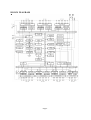
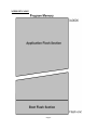
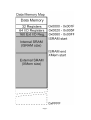
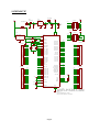
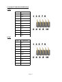
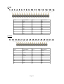
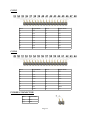
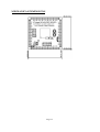
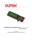
AVR- H128-CAN development board
Users Manual
All boards produced by Olimex are ROHS compliant
Rev.A, January 2005
Copyright(c) 2009, OLIMEX Ltd, All rights reserved
Page1
INTRODUCTION
AVR-H128-CAN is inexpensive way to develop and prototype circuits with
AT90CAN128 without need to deal with SMD soldering. All microcontroller pins
are available on extension header with 0.1" and power supply, oscillators, ICSP,
JTAG are wired, so all you need to do is to connect your additional components to
the AVR ports, as the step is 0.1" these headers perfectly fit the prototype sea of pad
boards with 0.1" step.
BOARD FEATURES
–
AT90CAN128-16AU microcontroller with 128KB Flash, 4KB RAM, 4KB
EEPROM, CAN controller
–
ICSP 5x2 pin connector for in-circuit programming with AVR-PG1 or AVR-PG2
or STK500 compatible programmer
–
JTAG 5x2 pin connector for in-circuit debugging with AVR-JTAG-L or AVRJTAG-USB
–
16MHz scillator circuit
–
32768 Hz oscillator circuit
–
Reset IC ZM33064
–
+5V voltage regulator LM78L05
–
power supply filtering capacitors
–
extension pin headers for each uC pin
–
FR-4, 1.5 mm (0,062"), green soldermask, white silkscreen component print
–
dimensions 47x47 mm (1.85x1.85")
ELECTROSTATIC WARNING
The AVR-H128-CAN board is shipped in protective anti-static packaging. The
board must not be subject to high electrostatic potentials. General practice for
working with static sensitive devices should be applied when working with this
board.
BOARD USE REQUIREMENTS
Cables: The cable you will need depends on the programmer/debugger you use. If
you use AVR-JTAG or AVR-PG1 you will need RS232, if you use AVR-USB-JTAG
or AVR-ISP500/TINY/ISO you will need 1.8 m A-B USB cable, if you use AVRPG2, you will need LPT cable.
Hardware: One of OLIMEX Programmers/Debuggers – AVR-JTAG, AVR-USBJTAG, AVR-ISP500, AVR-ISP500-TINY, AVR-ISP500-ISO, AVR-PG1, AVR-PG2.
Software: AVR C compiler.
Page2
PROCESSOR FEATURES
AVR-H128-CAN board use High-performance, Low-power AVR® 8-bit
Microcontroller – AT90CAN128 from Atmel Corporation with these features:
–
–
Advanced RISC Architecture
–
133 Powerful Instructions – Most Single Clock Cycle Execution
–
32 x 8 General Purpose Working Registers + Peripheral Control
Registers
–
Fully Static Operation
–
Up to 16 MIPS Throughput at 16 MHz
–
On-chip 2-cycle Multiplier
Non volatile Program and Data Memories
–
128K Bytes of In-System Reprogrammable Flash
–
–
–
–
–
Endurance: 10,000 Write/Erase Cycles
Optional Boot Code Section with Independent Lock Bits
–
Selectable Boot Size: 1K Bytes, 2K Bytes, 4K Bytes or 8K Bytes
–
In-System Programming by On-Chip Boot Program (CAN,
UART, ...)
–
True Read-While-Write Operation
–
4K Bytes EEPROM (Endurance: 100,000 Write/Erase Cycles)
–
4K Bytes Internal SRAM
–
Up to 64K Bytes Optional External Memory Space
–
Programming Lock for Software Security
JTAG (IEEE std. 1149.1 Compliant) Interface
–
Boundary-scan Capabilities According to the JTAG Standard
–
Programming Flash (Hardware ISP), EEPROM, Lock & Fuse Bits
–
Extensive On-chip Debug Support
CAN Controller 2.0A & 2.0B - ISO 16845 Certified
–
15 Full Message Objects with Separate Identifier Tags and Masks
–
Transmit, Receive, Automatic Reply and Frame Buffer Receive Modes
–
1Mbits/s Maximum Transfer Rate at 8 MHz
–
Time stamping, TTC & Listening Mode (Spying or Autobaud)
Peripheral Features
–
Programmable Watchdog Timer with On-chip Oscillator
–
8-bit Synchronous Timer/Counter-0
–
10-bit Prescaler
–
External Event Counter
–
Output Compare or 8-bit PWM Output
Page3
–
–
–
8-bit Asynchronous Timer/Counter-2
–
10-bit Prescaler
–
External Event Counter
–
Output Compare or 8-Bit PWM Output
–
32Khz Oscillator for RTC Operation
Dual 16-bit Synchronous Timer/Counters-1 & 3
–
10-bit Prescaler
–
Input Capture with Noise Canceler
–
External Event Counter
–
3-Output Compare or 16-Bit PWM Output
–
Output Compare Modulation
8-channel, 10-bit SAR ADC
–
8 Single-ended Channels
–
7 Differential Channels
–
2 Differential Channels With Programmable Gain at 1x, 10x, or 200x
–
On-chip Analog Comparator
–
Byte-oriented Two-wire Serial Interface
–
Dual Programmable Serial USART
–
Master/Slave SPI Serial Interface
–
–
Programming Flash (Hardware ISP)
Special Microcontroller Features
–
Power-on Reset and Programmable Brown-out Detection
–
Internal Calibrated RC Oscillator
–
8 External Interrupt Sources
–
5 Sleep Modes: Idle, ADC Noise Reduction, Power-save, Power-down
& Standby
–
Software Selectable Clock Frequency
–
Global Pull-up Disable
–
Operating Voltages: 2.7 – 5.5V
–
Operating temperature: Industrial (-40°C to +85°C)
–
Maximum Frequency: 8 MHz at 2.7V, 16 MHz at 4.5V
–
53 Programmable I/O Lines
Page4
BLOCK DIAGRAM
Page5
MEMORY MAP:
Page6
Page7
SCHEMATIC
POWER 2
EPWR
U2
78L05
D1
1N4148
1
C6
100n
R1
IN
+5V
+5V
ICSP
2
1
+5V
PE0
OUT
C7
100n
GND
C3
100n
C4
100n
RESET
PB1
PE1
4.7K
1
3
5
7
9
2
4
6
8
10
+5V
+5V
JTAG
GND
C1
20pF Q1
RESET
XTAL1
24
23
16.000MHz/20pF
CON2
PEN
PE0
PE1
PE2
PE3
PE4
PE5
PE6
PE7
PB0
PB1
PB2
PB3
PB4
PB5
PB6
1
PB7
2 TOSC2
3 TOSC1
4 RESET
5
+5V
6
GND
7 XTAL2
8 XTAL1
PD0
9
PD1
10
PD2
11
PD3
12
PD4
13
PD5
14
PD6
15
PD7
16
Q2
C932KHz/6pF
20pF
1
2
3
4
5
6
7
8
9
10
11
12
13
14
15
16
XTAL2
TOSC1
TOSC2
20pF
C8
CON1
C2
20pF
+5V
20
19
18
PE0
PE1
PE2
PE3
PE4
PE5
PE6
PE7
2
3
4
5
6
7
8
9
PD0
PD1
PD2
PD3
PD4
PD5
PD6
PD7
25
26
27
28
29
30
31
32
PF0
PF1
PF2
PF3
TCK
TMS
TDO
TDI
61
60
59
58
57
56
55
54
+5V
64
C5
AREF
62
100n
GND
63
TCK
TDO
TMS
21
52
IC1
RESET 3
1
2 VCC
RESET/
VCC
XTAL1
XTAL2
TDI
TOSC1
TOSC2
RXD-PE0
TXD-PE1
AC+_PE2
AC-_PE3
INT4-PE4
INT5-PE5
INT6-PE6
INT7-PE7
PD0-INT0
PD1-INT1
PD2-INT2
PD3-INT3
PD4-IC1
PD5
PD6-T1
PD7-T2
ADC0-PF0
ADC1-PF1
ADC2-PF2
ADC3-PF3
ADC4-PF4
ADC5-PF5
ADC6-PF6
ADC7-PF7
PA0
PA1
PA2
PA3
PA4
PA5
PA6
PA7
35
36
37
38
39
40
41
42
PC0
PC1
PC2
PC3
PC4
PC5
PC6
PC7
17
16
15
14
13
12
11
10
PB7
PB6
PB5
PB4
PB3
PB2
PB1
PB0
43
ALE 34
RD/ 33
WR/ 1
PEN/
ALE
RD
WR
PEN
AD0-PA0
AD1-PA1
AD2-PA2
AD3-PA3
AD4-PA4
AD5-PA5
AD6-PA6
AD7-PA7
A8-PC0
A9-PC1
A10-PC2
A11-PC3
A12-PC4
A13-PC5
A14-PC6
A15-PC7
OC2-PB7
OC1B-PB6
OC1A-PB5
OC0-PB4
MISO-PB3
MOSI-PB2
SCK-PB1
SS-PB0
AVCC
AVREF
AGND
51
50
49
48
47
46
45
44
1
3
5
7
9
PA2
PA1
PA0
+5V
GND
TDI
TDO
TMS
TCK
PF3
PF2
PF1
PF0
AREF
GND
+5V
1
2
3
4
5
6
7
8
9
10
11
12
13
14
15
16
WR
RD
PC0
PC1
PC2
PC3
PC4
PC5
PC6
PC7
ALE
PA7
PA6
PA5
PA4
PA3
1
2
3
4
5
6
7
8
9
10
11
12
13
14
15
16
CON3
+5V
R2
1K
GND
ATMEGA128CAN
2
4
6 RESET
8
10
CON4
53
22
U1
ZM33064
AVR-H128-CAN
Rev. A
COPYRIGHT(C), 2005
http://www.olimex.com/dev
Page8
BOARD LAYOUT
Page9
POWER SUPPLY CIRCUIT
The board is power supplied from POWER connector pin 1 and pin 2 with 9-12 V
DC.
RESET CIRCUIT
AVR-H128-CAN reset circuit includes pin 6 of JTAG connector, pin 5 of ICSP
connector, Extension connector CON2 – pin 4 and AT90CAN128 pin 20.
CLOCK CIRCUIT
Quartz crystal 16MHz is connected to AT90CAN128 pin 23 (XTAL2) and pin 24
(XTAL1).
Quartz crystal 32kHz is connected to AT90CAN128 pin 18 (TOSC2) and pin 19
(TOSC1).
JUMPER DESCRIPTION
EPWR
Enable target power supply.
Page10
CONNECTOR DESCRIPTIONS
JTAG
Pin #
Signal Name
1
TCK
2
GND
3
TDO
4
+5V
5
TMS
6
RESET
7
+5V
8
NC
9
TDI
10
GND
ICSP
Pin #
Signal Name
1
PE0
2
+5V
3
NC
4
GND
5
RESET
6
GND
7
PB1
8
GND
9
PE1
10
GND
Page11
CON1
Pin #
Signal Name
Pin #
Signal Name
1
PEN
2
PE0
3
PE1
4
PE2
5
PE3
6
PE4
7
PE5
8
PE6
9
PE7
10
PB0
11
PB1
12
PB2
13
PB3
14
PB4
15
PB5
16
PB6
Pin #
Signal Name
Pin #
Signal Name
17
PB7
18
TOSC2
19
TOSC1
20
RESET
21
+5V
22
GND
23
XTAL2
24
XTAL1
25
PD0
26
PD1
27
PD2
28
PD3
29
PD4
30
PD5
31
PD6
32
PD7
CON2
Page12
CON3
Pin #
Signal Name
Pin #
Signal Name
33
WR
34
RD
35
PC0
36
PC1
37
PC2
38
PC3
39
PC4
40
PC5
41
PC6
42
PC7
43
ALE
44
PA7
45
PA6
46
PA5
47
PA4
48
PA3
Pin #
Signal Name
Pin #
Signal Name
49
PA2
50
PA1
51
PA0
52
+5V
53
GND
54
TDI
55
TDO
56
TMS
57
TCK
58
PF3
59
PF2
60
PF1
61
PF0
62
AREF
63
GND
64
+5V
CON4
POWER CONNECTOR
Pin #
Signal Name
1 (+)
VCC
2 (-)
GND
Page13
MECHANICAL DIMENSIONS
Page14
AVAILABLE DEMO SOFTWARE
–
–
Blinking LED C source for WinAVR
UART initialization C source for WinAVR
Page15
ORDER CODE
AVR-H128-CAN – assembled and tested board, includes AT90CAN128-16
microcontroller.
How to order?
You can order to us directly or by any of our distributors.
Check our web www.olimex.com/dev for more info.
Revision history:
REV.A
- create January 2005
Page16
Disclaimer:
© 2009 Olimex Ltd. All rights reserved. Olimex®, logo and combinations thereof, are registered trademarks of
Olimex Ltd. Other terms and product names may be trademarks of others.
The information in this document is provided in connection with Olimex products. No license, express or implied
or otherwise, to any intellectual property right is granted by this document or in connection with the sale of
Olimex products.
Neither the whole nor any part of the information contained in or the product described in this document may be
adapted or reproduced in any material from except with the prior written permission of the copyright holder.
The product described in this document is subject to continuous development and improvements. All particulars
of the product and its use contained in this document are given by OLIMEX in good faith. However all warranties
implied or expressed including but not limited to implied warranties of merchantability or fitness for purpose are
excluded.
This document is intended only to assist the reader in the use of the product. OLIMEX Ltd. shall not be liable for
any loss or damage arising from the use of any information in this document or any error or omission in such
information or any incorrect use of the product.
Page17