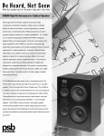
1
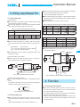
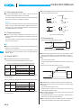
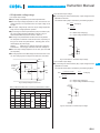
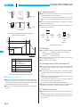
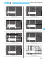
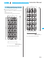
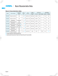
Basic Characteristics Data
Basic Characteristics Data
Circuit method
Switching
frequency
[kHz]
Input
current
Rated
input fuse
Inrush
current
protection
Material
CHS60
Foward converter
440
*1
-
-
CHS80
Half-bridge converter
250
*1
-
-
CHS200
Full-bridge converter
150
*1
-
CHS300
Full-bridge converter
170
*1
-
CHS400
Full-bridge converter
150
*1
CHS500
Full-bridge converter
150
*1
Model
*1 R
efer to Specification.
*2 R
efer to Instruction Manual.
CHS
CHS-16
Series/Redundancy
operation availability
PCB/Pattern
Single
sided
Double
sided
Series
operation
Redundancy
operation
glass fabric base, epoxy resin
Multilayer
Yes
*2
glass fabric base, epoxy resin
Multilayer
Yes
*2
-
glass fabric base, epoxy resin
Multilayer
Yes
*2
-
glass fabric base, epoxy resin
Multilayer
Yes
*2
-
-
glass fabric base, epoxy resin
Multilayer
Yes
*2
-
-
glass fabric base, epoxy resin
Multilayer
Yes
*2
DC-DC Converters Bus Converter.Power Module Type
Instruction Manual
1
Pin Connection
CHS-18
2
Connection for Standard Use
CHS-18
3
Wiring Input/Output Pin
CHS-19
4
5
6
3.1
Wiring input pin
CHS-19
3.2
Wiring output pin
CHS-19
Function
CHS-19
4.1 Overcurrent protection CHS-19
4.2 Overvoltage protection CHS-20
4.3 Thermal protection
CHS-20
4.4
Remote ON/OFF
CHS-20
4.5
Remote sensing
CHS-20
4.6
Adjustable voltage range
CHS-21
4.7Isolation
CHS-22
4.8
CHS-22
PMBus interface
Series and Parallel Operation
CHS-22
5.1
Series operation
CHS-22
5.2 Parallel operation
CHS-22
5.3 Redundancy operation
CHS-22
Implementation-Mounting Method
CHS-23
6.1 Mounting method CHS-23
6.2 Automatic Mounting (CHS series:option S)
CHS-23
6.3 Soldering CHS-23
6.4
Stress onto the pins
CHS-24
6.5Cleaning
CHS-24
6.6
Storage method (CHS series:option S)
CHS-24
6.7
Stress to the product
CHS-24
7
Safety Considerations
CHS-25
8
Derating
CHS-25
8.1
9
CHS Derating
SMD type(optionS) package information
CHS-25
CHS-29
CHS-17
CHS
DC-DC Converters Bus Converter . Power Module Type
Table 1.1 Pin Connection and function
1 Pin Connection
No.
Pin Connection
1
+VIN
2
RC
Remote ON/OFF
3
-VIN
-DC input
4
+VOUT
¿CHS60
-VIN 3
RC 2
+VIN 1
8 -VOUT
7 -S
6 TRM
5 +S
4 +VOUT
¿CHS80
RC 2
+VIN 1
CHS
8 -VOUT
7 -S
RC 2
6 TRM
5 +S
4 +VOUT
+VIN 1
+S
6
TRM
+DC output
+Remote sensing
Adjustment of output voltage
-S
8
-VOUT
No.
Pin Connection
1
+VIN
¿CHS200
-VIN 3
5
Function
+DC input
7
8 -VOUT
7 -S
6 TRM
5 +S
4 +VOUT
-VIN 3
Instruction Manual
-Remote sensing
-DC output
Reference
3.1 ”Wiring input pin ”
2
RC
4.4 ”Remote ON/OFF ”
3
-VIN
3.1 ”Wiring input pin ”
4
+VOUT
3.2 ”Wiring output pin ”
5
+S
4.5 ”Remote sensing ”
6
TRM
7
-S
4.5 ”Remote sensing ”
8
-VOUT
3.2 ”Wiring output pin ”
4.6 ”Adjustable voltage range ”
2 Connection for Standard Use
¡In order to use the power supply, it is necessary to wire as shown
in Fig.2.1.
¿CHS300
-VIN 3
8 -VOUT
7 -S
RC 2
6 TRM
5 +S
4 +VOUT
+VIN 1
Reference : 3 ”Wiring Input/Output Pin”
¡Short the following pins to turn on the power supply.
-VIN RC, +VOUT +S, -VOUT -S
Reference : 4.4 ”Remote ON/OFF”
¿CHS400/CHS500
-VIN 3
8 -VOUT
7 -S
RC 2
6 TRM
5 +S
4 +VOUT
+VIN 1
8 ”Derating”
4.5 ”Remote sensing”
¡The CHS series handle only the DC input.
Avoid applying AC input directly.
It will damage the power supply.
Fuse
+VIN
Cin +
DC
input
RC
-VIN
+VOUT
+S
Load
-S
-VOUT
Cin : External capacitor on the input side
Fig.1.1 Pin Connection (bottom view)
Fig.2.1 Connection for standard use
Table 2.1 Recommended External capacitor on the input side
Model
CHS30024
Cin
660 F or more
Model CHS6048
CHS-18
CHS8048
CHS20048 CHS30048/CHS40048/CHS50048
Cin 66 F or more 33 F or more 100 F or more
200 F or more
DC-DC Converters Bus Converter . Power Module Type
3 Wiring Input/Output Pin
In this case, please install a capacitor Co.
wiring impedance.
(1) External fuse
¡Fuse is not built-in on input side. In order to protect the unit, install
the normal-blow type fuse on input side.
¡When the input voltage from a front end unit is supplied to multiple
units, install the normal-blow type fuse in each unit.
Table 3.1 Recommended fuse (Normal-blow type)
Model
CHS30024
Rated current
20A
Model
CHS6048 CHS8048 CHS20048/CHS30048 CHS40048 CHS50048
5A
¡If output current decreases rapidly, output voltage rises transiently
and the overvoltage protection circuit may operate.
¡Select a high frequency type capacitor. Output ripple and startup
waveform may be influenced by ESR-ESL of the capacitor and the
3.1 Wiring input pin
Rated current
Instruction Manual
7A
15A
20A
30A
¡Make sure that ripple current of Co is than its rating.
Table 3.2 Recommended capacitance Co (CHS60, CHS80, CHS200)
No.
Output voltage
CHS60
CHS80
CHS200
1
3.3V
0 - 20,000 F
0 - 20,000 F
0 - 40,000 F
2
5V
0 - 10,000 F
0 - 10,000 F
0 - 20,000 F
3
12V
0 - 2,200 F
0 - 1,000 F
0 - 2,200 F
Table 3.3 Recommended capacitance Co (CHS300, CHS400, CHS500)
No.
Output voltage
CHS300
CHS400/CHS500
(2) External capacitor on the input side
1
5V
0 - 20,000 F
-
¡Install an external capacitor Cin, between +VIN and -VIN input
pins for low line-noise and for stable operation of the power sup-
2
10V
0 - 2,200 F
0 - 4,000 F
3
12V
0 - 2,200 F
0 - 4,000 F
4
15V
0 - 2,200 F
ply.
Capacitance
Refer to Table 2.1
Ta = -20 to +85C Electrolytic or Ceramic capacitor
Ta = -40 to +85C Ceramic capacitor
-
¡Ripple and Ripple Noise are measured, as shown in the Fig.3.3.
Cin is shown in Table 2.1.
50mm
¡Cin is within 50mm for pins. Make sure that ripple current of Cin
is less than its rating.
(3) Recommendation for noise-filter
¡Install an external input filter as shown in Fig.3.1 in order to reduce conducted noise. Cin is shown in Table 2.1.
Measuring
board
+VIN +VOUT
DC
Input
Cin
+S
+
RC
-S
Co
22 F
Load
-VIN -VOUT
1mH
DC
input
+VIN
+
2. 2 F
Cin
RC
-VIN
0.068
F
0.068 F
+VOUT
+S
-S
-VOUT
+
10 F
0.033 F
Load
Oscilloscope
BW:100MHz
0.033 F
C
FG
Fig.3.1 Recommended external input filter
R
1.5m 50W
Coaxial cable
R=50W
C=0.01 F
Fig.3.3 Measuring method of Ripple and Ripple Noise
(4) Reverse input voltage protection
¡Avoid the reverse polarity input voltage. It will damage the power
supply.
It is possible to protect the unit from the reverse input voltage by
installing an external diode as shown in Fig.3.2.
+VIN
DC IN
-VIN
Fig.3.2 Reverse input voltage protection
3.2 Wiring output pin
¡When the CHS series supplies the pulse current for the pulse
load, please install a capacitor Co between +VOUT and -VOUT
pins.
4Function
4.1 Overcurrent protection
¡Over Current Protection (OCP) is built-in and works at 105% of
the rated current or higher. However, use in an overcurrent situation must be avoided whenever possible.
The output voltage of the power module will recover automatically
when the fault causing overcurrent is corrected.
When the output voltage drops after OCP works, the power module enters a ”hiccup mode” where it repeatedly turns on and off at
a certain frequency.
Recommended capacitance of Co is shown in Table 3.2, 3.3.
CHS-19
CHS
Instruction Manual
DC-DC Converters Bus Converter . Power Module Type
4.2 Overvoltage protection
¡The overvoltage protection circuit is built-in. The DC input will be
shut down if overvoltage protection is in operation.
¡When remote ON/OFF function is not used, please short between RC and
-VIN (-R: open between RC and -VIN).
Vcc
(2.0[Vcc[7.0V)
The output voltage of the power module will recover automatically
RC
when the fault causing over voltage is corrected.
-VIN
Remarks :
-VIN
Photo coupler
Please note that devices inside the power supply might fail when
voltage more than rated output voltage is applied to output pin of
the power supply. This could happen when the customer tests the
overvoltage performance of the unit.
4.3 Thermal protection
Transistor
RC
RC
-VIN
-VIN
IC
¡When the power supply temperature is kept above 120C, the
thermal protection will be activated and simultaneously shut down
the output.
The output voltage of the power supply will recover automatically
when the unit is cool down.
Relay
Fig.4.1 RC connection example
4.5 Remote sensing
(1) When the remote sensing function is not in use
+VOUT
¿-U
+S
-S
-VOUT
¡Option ”-U” means output is shut down when the abovementioned
protection circuit is activated.
If this happens, protection circuit can be inactivated by cycling
CHS
RC
¡When the remote sensing function is not in use, it is necessary to confirm
that pins are shorted between +S & +VOUT and between -S & -VOUT.
4.4 Remote ON/OFF
¡Remote ON/OFF circuit is built-in on the input side (RC).
The ground pin of input side remote ON/OFF circuit is ”-VIN” pin.
Table 4.1.1 Specification of Remote ON/OFF(CHS80,CHS200)
ON/OFF
logic
Standard
Negative
Optional -R
Positive
Between RC and -VIN
L level(0 - 0.8V) or short
H level(2.0 - 7.0V) or open
L level(0 - 0.8V) or short
H level(2.0 - 7.0V) or open
Output
¡Wire between +S & +VOUT and between -S & -VOUT as short as possible.
Loop wiring should be avoided.
This power supply might become unstable by the noise coming from poor
wiring.
(2)When the remote sensing function is in use
Wire as close as possible
voltage
ON
OFF
OFF
ON
+VOUT
+S
-S
-VOUT
When RC is ”Low” level, fan out current is 0.1mA typ. When Vcc is applied,
use 2.0[Vcc[7.0V.
Table 4.1.2 Specification of Remote ON/OFF(CHS60,CHS300,CHS400,CHS500)
ON/OFF
logic
Standard
Negative
Optional -R
Positive
Between RC and -VIN
L level(0 - 0.8V) or short
H level(4.0 - 7.0V) or open
L level(0 - 0.8V) or short
H level(4.0 - 7.0V) or open
Output
voltage
ON
OFF
OFF
ON
When RC is ”Low” level, fan out current is 0.1mA typ. When Vcc is applied,
use 4.0[Vcc[7.0V.
Short at pin root
Fig.4.2 Connection when the remote sensing is not in use
the DC input power off for at least 1 second or toggling Remote
ON/OFF signal.
Load
Load
Fig.4.3 Connection when the remote sensing is in use
¡Twisted-pair wire or shield wire should be used for sensing wire.
¡Thick wire should be used for wiring between the power supply
and a load.
Line drop should be less than 0.3V.
Voltage between +VOUT and -VOUT should remain within the
output voltage adjustment range.
¡If the sensing patterns are short, heavy-current is drawn and the
pattern may be damaged.
The pattern disconnection can be prevented by installing the protection parts as close as possible to a load.
¡Output voltage might become unstable because of impedance of
wiring and load condition when length of wire exceeds 40cm.
CHS-20
DC-DC Converters Bus Converter . Power Module Type
4.6 Adjustable voltage range
Instruction Manual
(2) To decrease output voltage
(1) To adjust output voltage
¡Output voltage is adjustable by the external potentiometer.
¡When the output voltage adjustment is used, note that the over
¡By connecting the external resistor (RD), output voltage becomes
adjustable to decrease.
The external resistor (RD) is calculated by the following equation.
voltage protection circuit operates when the output voltage is set
RD=
too high.
¡If the output voltage drops under the output voltage adjustment
range, the Low voltage protection operates.
¡By connecting the external potentiometer (VR1) and resistors (R1,
R2), output voltage becomes adjustable, as shown in Fig.4.4.
Recommended external parts are shown in Table 4.2.
Δ=
5.11
Δ
-10.22 [kW]
VOR-VOD
VOR
VOR : Rated output voltage [V]
VOD : Output voltage needed to set up [V]
¡The wiring to the potentiometer should be as short as possible.
The temperature coefficient could become worse, depending on
+VOUT
+S
the type of a resistor and potentiometer. Following parts are recommended for the power supply.
Resistor.............Metal film type, coefficient of less than ±100ppm/C
Potentiometer....Cermet type, coefficient of less than ±300ppm/C
TRM
RD
¡When the output voltage adjustment is not used, open the TRM
pin respectively.
-S
-VOUT
¡The change speed of the TRM voltage should be less than 0.15V/
ms, when changing output voltage to less than 90% of the rated.
Fig.4.5 Connection to decrease output voltage
+VOUT
(3) To increase output voltage
+S
Control Amp.
of rated
voltage
R1
RA
5.11kW
1.225V
+
TRM
R2
RC
5.11kW
¡By connecting the external resistor (RU), output voltage becomes
adjustable to increase.
The external resistor (RU) is calculated by the following equation.
VR1
5kW
RU=
Δ=
-S
-VOUT
Fig.4.4 Output voltage control circuit
Table 4.2 Recommended value of external potentiometer & resistor
Output adjustable range
No.
VOUT
VOUT ±5%
R1
R2
5.11XVORX(1+Δ)
1.225XΔ
R1
R2
1
3.3V
2.2kW
68kW
2.2kW
33kW
2
5V
4.7kW
68kW
5.6kW
33kW
3
10V
15kW
68kW
15kW
33kW
4
12V
18kW
68kW
18kW
33kW
5
15V
22kW
68kW
22kW
33kW
5kW
VR1
5kW
5.11
Δ
- 10.22 [kW]
VOU-VOR
VOR
VOR : Rated output voltage [V]
VOU : Output voltage needed to set up [V]
+VOUT
+S
RU
VOUT ±10%
VR1
-
TRM
-S
-VOUT
Fig.4.6 Connection to increase output voltage
CHS-21
CHS
DC-DC Converters Bus Converter . Power Module Type
(4) Input voltage derating
115
the time of the use with this option.
12V
110
¡As variance of output current drew from each power supply is
maximum 10%, the total output current must not exceed the value
15V
105
100
determined by the following equation.
80
0
0
18
(Output current in parallel operation)
36
20 21.5
INPUT VOLTAGE [V]
=(the rated current per unit) x (number of unit) x0.9
When the number of units in parallel operation increases, input
5V
120
3.3V
115
12V
110
105
100
95
3.3V,5V
90
12V
80
0
36
40
76
INPUT VOLTAGE [V]
CHS6048
ADJUSTMENT RANGE [%]
ADJUSTMENT RANGE [%]
CHS30024
0
5V
120
3.3V
115
10V,12V
110
105
100
95
put circuitry is required, such as circuit pattern, wiring and current
capacity for equipment.
and load, and line drop should be less than 0.3V.
90
80
0
current increase at the same time. Adequate wiring design for in-
¡Total number of units should be no more than 3 pieces.
¡Thick wire should be used for wiring between the power supply
4812H
0
36
40
44
INPUT VOLTAGE [V]
76
CHS8048/CHS20048/CHS30048/
CHS40048/CHS50048
Fig.4.7 CHS Output Voltage Adjustment Range
¡Connect each input pin for the lowest possible impedance.
¡When the number of the units in parallel operation increases,
inputcurrent increases. Adequate wiring design for input circuitry
such as circuit pattern, wiring and current for equipment is required.
DC
INPUT
4.7 Isolation
Fuse
¡For a receiving inspection, such as Hi-Pot test, gradually increase
(decrease) the voltage to start (shut down). Avoid using Hi-Pot
Fuse
higher than the applied voltage at ON/OFF of a timer.
4.8 PMBus interface
RC
+Vin
+Vout
-Vin
-Vout
¡Parallel operation is not possible.
¡Redundancy operation is available by wiring as shown below.
Power +
Supply
-
5.1 Series operation
¡Series operation is available by connecting the outputs of two or
more power supplies, as shown below. Output current in series
connection should be lower than the lowest rated current in each
Power +
Supply
-
Load
Power +
Supply -
I1
I3
I2
Fig.5.3 Redundancy operation
¡Even a slight difference in output voltage can affect the balance
between the values of I1 and I2.
Power +
Supply -
Load
(b)
Fig.5.1 Examples of series operation
CHS-22
-Vout
5.3 Redundancy operation
5 Series and Parallel Operation
Power +
Supply -
-Vin
Fig.5.2 Examples of parallel operation
¡This option is equipped with a digital PMBus interface.
Please contact us about for details.
Power +
Supply -
+Vout
RC
¿-I (CHS300/CHS400)
unit.
(a)
+Vin
LOAD
SW
tester with timer because it may generate voltage a few times
Load
CHS
¿-P (CHS400/CHS500)
¡This option is for parallel operation.
¡Sensing and adjustment of the output voltage are not possible at
5V
120
5.2 Parallel operation
Load
ADJUSTMENT RANGE [%]
¡When input voltage is 18-21.5V DC or 36-44VDC, the output
voltage adjustment range becomes as shown in Fig.4.7.
Instruction Manual
Please make sure that the value of I3 does not exceed the rated
current of the power supply.
I3[the rated current value
DC-DC Converters Bus Converter . Power Module Type
6 Implementation-Mounting Method
Instruction Manual
48
1.5
+VIN
6.1 Mounting method
¡The unit can be mounted in any direction. When two or more power supplies are used side by side, position them with proper inter-
RC
vals to allow enough air ventilation. The temperature around each
-VIN
+VOUT
+S
TRM
-S
-VOUT
power supply should not exceed the temperature range shown in
(d) CHS300
derating curve.
¡Avoid placing the DC input line pattern layout underneath the unit.
It will increase the line conducted noise. Make sure to leave an
8
41
ample distance between the line pattern layout and the unit. Also
avoid placing the DC output line pattern underneath the unit because it may increase the output noise. Lay out the pattern away
from the unit.
¡Avoid placing the signal line pattern layout underneath the unit because the power supply might become unstable.
Lay out the pattern away from the unit.
¡Avoid placing pattern layout in hatched area shown in Fig.6.1 to
insulate between pattern and power supply.
7
+VIN
+VOUT
+S
TRM
-S
-VOUT
RC
-VIN
(e) CHS400
5
Dimensions in mm
+VOUT
+S
TRM
-S
-VOUT
RC
13
1
+VIN
-VIN
2
6.2 Automatic Mounting (CHS series:option S)
¡To mount CHS series automatically, use the inductor area near the
output pin as an adsorption point. Please see the External View
10
for details of the adsorption point.
(a) CHS60
5
If the bottom dead point of a suction nozzle is too low when
mounting excessive force is applied to the inductor, it could cause
14
damage. Please mount carefully.
+VIN
+VOUT
+S
TRM
-S
-VOUT
RC
-VIN
6.3 Soldering
(1)Flow Soldering :260C (2)Soldering Iron
(b) CHS80
37
5
CHS
Fig.6.1 Prohibition area of pattern layout (top view)
15 seconds or less
:maximum 450C 5 seconds or less
(3)Reflow Soldering (option “-S”)
¡Fig.6.2 shows conditions for the reflow soldering for option “-S”
of CHS series. Please make sure that the temperatures of pin
8
24
terminals +VIN and -VOUT shown in Fig.6.2 do not exceed the
+VIN
+VOUT
+S
TRM
-S
-VOUT
RC
-VIN
temperatures shown in Fig.6.3.
¡If time or temperature of the reflow soldering goes beyond the
conditions, reliability of internal components may be compromised.
Please use the unit under the recommended reflow conditions.
(c) CHS200
CHS-23
Instruction Manual
DC-DC Converters Bus Converter . Power Module Type
6.4 Stress to the pins
+VIN
-VOUT
¡When too much stress is applied to the pins of the power supply,
the internal connection may be weakened.
As shown in Fig.6.4, avoid applying stress of more than 19.6N
(2kgf) to the pins horizontally and more than 39.2N (4kgf) verti-
(a) CHS60
cally.
¡The pins are soldered on PWB internally. Therefore, do not pull or
bend them with strong force.
+VIN
-VOUT
¡Fix the unit on PCB (using silicone rubber or fixing fittings) to reduce the stress to the pins.
(b) CHS80
Fig.6.2 Temperature Measuring Points when Setting
Less than
19.6N
Reflow Soldering Conditions
C
Less than
19.6N
Less than
19.6N
Less than
39.2N
Less than
39.2N
Tp
Less than
19.6N
(option S)
Tx
Fig.6.4 Stress to the pins
Ty2
6.5 Cleaning
Ty1
¡When cleaning is necessary, clean under the following conditions.
Method
: Varnishing, ultrasonic wave and vapor
CHS
A
A’
B
B'
C
time(s)
A
A'
1.0 - 5.0C/s
Ty1:160±10C
Ty2:180±10C
B
B'
Ty1 - Ty2:120s max
1.0 - 5.0C/s
Tp:Max245C 10s max
C
Tx:220C or more:70s max
1.0 - 5.0C/s
Fig.6.3 Recommend Reflow Soldering Conditions
¿Notes to use option “-S”
¡Solder iron or other similar methods are not recommended soldering method for option “-S” because it may not be able to retain
connection reliability between the PCB and the Pins. Solder reflow
is the acceptable mounting system for the option.
¡Option “-S” is not reusable product after soldered on any application PCB.
Cleaning agents : IPA (Solvent type)
Total time
: 2 minutes or less
¡Do not apply pressure to the lead and name plate with a brush or
scratch it during the cleaning.
¡After cleaning, dry them enough.
6.6 Storage method (CHS series:option S)
¡To stock unpacked products in your inventory, it is recommended
to keep them under controlled condition, 5-30C, 60%RH and use
them within a year.
¡24-hour baking is recommended at 125C, if unpacked products
were kept under uncontrolled condition, which is 30C, 60%RH or
higher.
Original trays are not heat-resistant. Please move them to heatresistant trays in preparation to bake.
To check moisture condition in the pack. Silica gel packet has
some moisture condition indicator particles.
Indicated blue means good. Pink means alarm to bake it.
¡Notification. The tray will be deformed and the power supply might
be damaged, if the vacuum pressure is too much to reseal.
6.7 Stress to the product
¡CHS series transformer core and choke coil core are attached by
glue.
There is a possibility that the core will be removed and power supply will be damaged when they receive stress by the fall or some
kind of stress.
CHS-24
DC-DC Converters Bus Converter . Power Module Type
Instruction Manual
7 Safety Considerations
¡To apply for safety standard approval using this power supply, the
following conditions must be met.
¿This unit must be used as a component of the end-use equipment.
¿The equipment must contain basic insulation between input and
output. If double or reinforced insulation is required, it has to be
Temperature measurement location
Fig.8.2.2 Temperature measurement location (CHS80)
provided by the end-use equipment in accordance with the final
build-in condition.
¿Safety approved fuse must be externally installed on input side.
8Derating
Temperature measurement location
¡It is necessary to note thermal fatigue life by power cycle.
Please reduce the temperature fluctuation range as much as pos-
Fig.8.2.3 Temperature measurement location (CHS200)
sible when the up and down of temperature are frequently generated.
8.1 CHS Derating
¡Use with the convection cooling or the forced air cooling.
Make sure the temperatures at temperature measurement locations shown from Fig.8.2.1 to Fig.8.2.8 below are on or under the
derating curve in Fig.8.1.
CHS
Temperature measurement location
Fig.8.2.4 Temperature measurement location (CHS300)
Ambient temperature must be kept at 85C or under.
100
3
Load factor[%]
80
1Option “B”
2Option “BC”
3Others
60
2
1
40
Temperature measurement location
20
0
-40
Fig.8.2.5 Temperature measurement location (CHS400)
-20
0
20
40
60
80
100
(95)
Temperature of measurement location[C]
120
Fig.8.1 Derating curve
Temperature measurement location
Temperature measurement location
Fig.8.2.6 Temperature measurement location (CHS500)
Fig.8.2.1 Temperature measurement location (CHS60)
CHS-25
DC-DC Converters Bus Converter . Power Module Type
Instruction Manual
20
¡For option “B” which is used with the convection cooling, forced
air cooling or conduction cooling, use the temperature measure-
3
18
2
16
Load current[A]
ment location as shown in Fig.8.2.7 and Fig.8.2.8.
12
10
8
6
4
Aluminum base plate
1
14
1convection cooling(0.2m/s)
21m/s
32m/s
2
0
-40
Measurement point
-30
-20
-10
0
10
20
30
40
50
60
70
80
Fig.8.2.7 Measurement point (CHS200/CHS300 option “B” and “BC”)
Fig.8.4 Load current vs. ambient temperature(CHS60483R3 Vin=48V)
14
2
3
Load current[A]
12
Aluminum base plate
Measurement point
1
10
8
6
4
1convection cooling(0.2m/s)
21m/s
32m/s
2
Fig.8.2.8 Measurement point (CHS400/CHS500 option “B”)
CHS
¡Shown the thermal curve with measuring as shown in Fig.8.3.
Verify final design by actual temperature measurement.
Use the temperature measurement location as shown in Fig.8.2.1
0
-40
-30
-20
-10
0
10
20
30
40
50
60
70
80
Fig.8.5 Load current vs. ambient temperature(CHS604805 Vin=48V)
7
3
6
Output side
CHS
2
5
1
4
3
2
1convection cooling(0.2m/s)
21m/s
32m/s
1
Measurement point for
ambient temperature
and airflow
12.7mm
76mm
Input side
CHS
Load current[A]
PWB
25.4mm
90
Ambient temperature[C]
to Fig.8.2.6 at 120C or less.
Top
90
Ambient temperature[C]
0
-40
-30
-20
-10
0
10
20
30
40
50
60
70
80
90
Ambient temperature[C]
Fig.8.6 Load current vs. ambient temperature(CHS604812 Vin=48V)
30
Airflow
Airflow
Fig.8.3 Measuring method
Load current[A]
25
15
10
3
1
20
2
1convection cooling(0.2m/s)
21m/s
32m/s
5
0
-40
-30
-20
-10
0
10
20
30
40
50
60
70
80
90
Ambient temperature[C]
Fig.8.7 Load current vs. ambient temperature(CHS80483R3 Vin=48V)
CHS-26
DC-DC Converters Bus Converter . Power Module Type
18
18
16
12
10
8
1convection cooling(0.2m/s)
21m/s
32m/s
6
4
3
14
2
Load current[A]
Load current[A]
16
3
1
14
10
8
1convection cooling(0.2m/s)
21m/s
32m/s
6
2
-30
-20
-10
0
10
20
30
40
50
60
70
80
0
-40
90
-30
-20
-10
0
Fig.8.8 Load current vs. ambient temperature(CHS804805 Vin=48V)
Load current[A]
Load current[A]
1convection cooling(0.2m/s)
21m/s
32m/s
-30
-20
-10
0
10
20
30
40
50
Ambient temperature[C]
60
70
80
80
90
25
20
15
0
-40
90
1convection cooling(0.2m/s)
21m/s
32m/s
-30
-20
-10
0
10
20
30
40
50
60
70
80
90
Ambient temperature[C]
Fig.8.13 Load current vs. ambient temperature(CHS3002405 Vin=24V)
18
60
16
50
1
40
14
3
2
Load current[A]
Load current[A]
70
5
Fig.8.9 Load current vs. ambient temperature(CHS804812 Vin=48V)
30
1convection cooling(0.2m/s)
21m/s
32m/s
20
10
-30
-20
-10
0
10
20
30
40
3
12
10
8
6
4
2
1
1convection cooling(0.2m/s)
21m/s
32m/s
2
50
60
70
80
0
-40
90
-30
-20
-10
Fig.8.10 Load current vs. ambient temperature(CHS200483R3 Vin=48V)
0
10
20
30
40
50
60
70
80
90
Ambient temperature[C]
Ambient temperature[C]
Fig.8.14 Load current vs. ambient temperature(CHS3002412 Vin=24V)
45
14
40
12
2
1
30
3
Load current[A]
35
Load current[A]
60
2
1
30
10
1
25
20
1convection cooling(0.2m/s)
21m/s
32m/s
15
10
-30
-20
-10
0
10
20
30
40
3
2
10
1
8
6
4
1convection cooling(0.2m/s))
21m/s
32m/s
2
5
0
-40
50
3
35
2
5
0
-40
40
40
3
1
6
0
-40
30
45
7
2
20
Fig.8.12 Load current vs. ambient temperature(CHS2004812 Vin=48V)
8
3
10
Ambient temperature[C]
Ambient temperature[C]
4
2
1
12
4
2
0
-40
Instruction Manual
50
60
70
80
90
Ambient temperature[C]
Fig.8.11 Load current vs. ambient temperature(CHS2004805 Vin=48V)
0
-40
-30
-20
-10
0
10
20
30
40
50
60
70
80
90
Ambient temperature[C]
Fig.8.15 Load current vs. ambient temperature(CHS3002415 Vin=24V)
CHS-27
CHS
DC-DC Converters Bus Converter . Power Module Type
32
35
28
2
1
20
Load current[A]
Load current[A]
30
3
24
16
12
8
1convection cooling(0.2m/s)
21m/s
32m/s
1
20
15
10
1convection cooling(0.2m/s)
21m/s
32m/s
-30
-20
-10
0
10
20
30
40
50
60
70
80
0
-40
90
-30
-20
-10
Fig.8.16 Load current vs. ambient temperature(CHS3004810 Vin=48V)
Load current[A]
Load current[A]
2
1
16
1convection cooling(0.2m/s)
21m/s
32m/s
4
-30
-20
-10
0
10
20
30
40
50
60
70
80
1
20
15
10
1convection cooling(0.2m/s)
21m/s
32m/s
-30
-20
-10
Load current[A]
Load current[A]
1
1convection cooling(0.2m/s)
21m/s
32m/s
20
30
40
50
60
70
80
90
20
15
-20
-10
0
10
20
30
40
50
60
70
80
90
40
3
2
30
1
25
1convection cooling(0.2m/s)
21m/s
32m/s
5
-30
-20
-10
0
10
20
30
40
50
1convection cooling(0.2m/s)
21m/s
32m/s
-30
-20
-10
0
10
20
30
40
50
60
70
80
90
Ambient temperature[C]
45
35
0
-40
2
1
25
5
-30
3
30
10
Fig.8.18 Load current vs. ambient temperature(CHS3004812H Vin=48V)
Load current[A]
10
35
Ambient temperature[C]
60
70
80
90
Ambient temperature[C]
Fig.8.19 Load current vs. ambient temperature(CHS4004810 Vin=48V)
CHS-28
0
Fig.8.21 Load current vs. ambient temperature(CHS4004812H Vin=48V)
2
4
0
-40
90
40
16
10
80
45
20
15
70
Ambient temperature[C]
3
24
20
60
2
25
0
-40
90
28
0
-40
50
5
Fig.8.17 Load current vs. ambient temperature(CHS3004812 Vin=48V)
8
40
3
Ambient temperature[C]
12
30
30
3
20
0
-40
20
35
24
CHS
10
Fig.8.20 Load current vs. ambient temperature(CHS4004812 Vin=48V)
28
8
0
Ambient temperature[C]
Ambient temperature[C]
12
3
2
25
5
4
0
-40
Instruction Manual
Fig.8.22 Load current vs. ambient temperature(CHS5004812 Vin=48V)
DC-DC Converters Bus Converter . Power Module Type
Instruction Manual
136
9 SMDtype(optionS)package information
38
23
38
48.55
34.1
¡These are packed in a tray (Fig.9.1 to Fig.9.2).
Please order “CHS60□□-S” or “CHS80□□-S” for tray type packaging.
Capacity of the tray is 15max.
In case of fractions, the units are stored in numerical order.
136
23
37
323
323
59×4=236
62X4=248
37
46.8
24.6
CHS
Dimensions in mm
Material : Conductive PS
Fig.9.2 Delivery package information (CHS80)
Dimensions in mm
Material : Conductive PS
Fig.9.1 Delivery package information (CHS60)
CHS-29