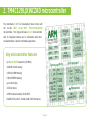
1
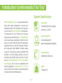
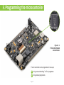
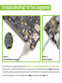
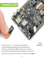
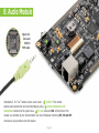
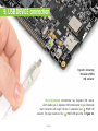
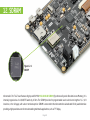
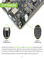
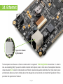
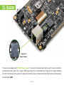
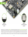
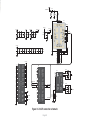
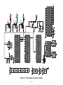
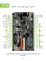
mikromedia 5 for Tiva™ Amazingly compact, all-on-a-single-pcb development board that carries 5’’ TFT Touch Screen and lots of multimedia peripherals, all driven by a powerful TM4C129L(X)NCZAD TO OUR VALUED CUSTOMERS I want to express my thanks to you for being interested in our products and for having confidence in MikroElektronika. The primary aim of our company is to design and produce high quality electronic products and to constantly improve the performance thereof in order to better suit your needs. Nebojsa Matic General Manager The Tiva™ and Windows® logos and product names are trademarks of Texas Instruments® and Microsoft® in the U.S.A. and other countries. Page 2 Table of Contents 4 8. Audio Module 22 System Specification 4 9. USB DEVICE connection 24 Package Contains 5 10. USB HOST connection 26 1. Power Supply 6 11. Accelerometer 28 2. TM4C129L(X)NCZAD microcontroller 8 12. SDRAM 30 Key microcontroller features 8 13. RF Transceiver 32 3. Programming the microcontroller 9 14. Ethernet 34 Introduction to mikromedia 5 for Tiva™ On-board mikroProg™ for Tiva® programmer 10 15. Buzzer 36 mikroProg Suite™ for ARM® software 12 16. WiFi 38 Software installation wizard 13 17. Other Modules 40 4. RTC Battery and Reset Button 14 18. Pads 42 5. Crystal Oscillators and 2.048 V Reference 16 19. Dimensions 44 6. microSD Card Slot 18 20. What’s next? 45 7. Touch Screen 20 Page 3 Introduction to mikromedia 5 for Tiva™ System Specification The mikromedia 5 for Tiva™ is a compact development board which allows development of devices with multimedia contents. The central part of the system is a 32-bit 212-pin TM4C129L(X)NCZAD microcontroller. The mikromedia 5 for Tiva™ features lots of on board modules such as stereo MP3 codec, 5’’ TFT 800x480 px touch screen display, accelerometer, microSD card slot, buzzer, IR receiver, RGB LED diode, PIN photodiode, temperature sensor, 2.4 GHz RF transceiver, Ethernet, Wi-Fi transceiver, 64Mb SDRAM, Li-Polimer battery charger etc. The board also contains two MINI-B USB connectors, 2x5 Cortex Debug connector, two 1x26 connection pads, ON/OFF switch and other. It comes with an on-board mikroProg™ for Tiva® programmer and debugger, but can also be programmed with external programmers. mikromedia 5 for Tiva™ is compact and slim, which makes it a convenient platform for mobile and other multimedia devices. power supply Via USB cable (5V DC) or via adapter connector (5 - 12 V DC) power consumption 121 mA with empty MCU (when on-board modules are disabled) board dimensions 135x86.6 mm (5.3x3.4 inch) weight ~136g (0.3 lbs) Page 4 Package Contains 01 Damage resistant protective box 02 mikromedia 5 for Tiva™ development board 03 Roll USB cable, roll ethernet cable and headers SCHEMATICS mikromedia 5 for Tiva™ Amazingly compact, all-on-single-pcb development board carring 5’’ TFT Touch Screen and lots of multimedia peripherals, all driven by powerful TM4C129LNCZAD mikromedia 5 for Tiva™ We present you with a complete color schematics for mikromedia 5 for Tiva development board. We want you to know what your board is consisted of and how it actually works. TM 04 mikromedia 5 for Tiva™ user’s guide 05 mikromedia 5 for Tiva™ schematic Page 5 06 Distancers, plastic pen and microSD card 1. Power Supply Figure 1-1: ICDI USB power supply Figure 1-2: USB power supply Figure 1-3: Battery power supply Figure 1-4: Adapter connector power supply The mikromedia 5 for Tiva™ board can be powered in four different ways: via two USB connectors using MINI-B USB cable provided with the board (CN9 or CN2), via battery connector using Li-Polymer battery (CN3) or via adapter connector using adapter power supply (CN1). After you plug in the appropriate power supply turn the power switch ON (SW1). The USB connection can provide up to 500 mA current which is more than enough for the operation of all on-board modules and the microcontroller as well. If you decide to use external power supply via adapter connector, voltage levels must be within 5-12 V DC range. Power LED ON (GREEN) indicates the presence of power supply. On-board battery charger circuit LM3658SD-A enables you to charge the battery over two USB connectors or via adapter connector. LED diode (RED) indicates when battery is charging. Charging current is ~250 mA and charging voltage is 4.2 V DC. Page 6 VCC-3.3V R2 10K USB-PSW# 4 5 VCC-5V VCC-3.3V R3 10K U5 EN 3 OC USB-VBUS_ER# Vusb_OUT 2 GND 1 IN OUT TPS2041B C6 100nF E1 10uF CN2 DC-VBUS# 3 DC-VBUS# 1 2 3 4 5 VIN PWR-EN Vusb-ICDI D2 B340A 10K D3 PMEG3010ER C7 22uF E2 10uF R9 C17 3.3nF CN3 R14 100K R18 100K V_INPUT BAT-VSENSE 3 2 M2 DMP2305U R13 100K SW1 JS202011AQN BAT-VSENSE 10 9 8 7 6 R6 1K C16 R7 10K 10 9 8 7 6 TPS63060 Vbat_IN R1 M4 DMG3420U R2 1K C8 C9 C10 C11 C12 22uF 22uF 22uF 1uF 100nF 10nF C13 C14 100pF VCC-3.3V R11 100K C27 R16 4K87 ±1% C18 C19 C20 C21 C22 22uF 22uF 22uF 1uF 100nF 10nF 10pF VCC-3.3V VCC-3.3V 1 2 3 4 5 C31 2.2uF U9 CHG_IN BATT USBpwr Ts GND PGND Iset USB_sel STAT1 STAT2 EN_b LM3658SD-A 10 9 8 7 6 R32 10K CHARGING CURRENT IS 250mA C30 1uF R26 10K M3 DMP2305U Vusb-ICDI R27 10K FP7 R29 560 BAT-STAT1 BAT-STAT2 LD2 R33 10K CHARGE BAT-STAT1 BAT-STAT2 1 R2 3 3 R1 100K R21 R22 10pF R15 12K C26 100nF 1K R28 10K E4 10uF VCC-5V R19 1K VCC-5V R31 10K 10K Q3 PDTC114EU VCC-1.8V R20 R4 100K C15 100nF L1 L2 VIN VOUT EN PGND FB PS GND VAUX PG C25 22uF C28 100nF R25 10K 2 R30 1 2 Vbat_IN Q2 PDTC114EU 4 AP7331-ADJ R23 R24 10K 5 U7 R12 100K 1 2 3 4 5 VIN PWR-EN VIN D7 ESDA5V3L V_INPUT EN ADJ L2 1.5uH Vbat_IN D6 ESDA5V3L TPS63060 R122 VIN 0 D5 B340A 10K USB-VBUS R10 1M GND V_INPUT R8 1K USB MINIB L1 L2 VIN VOUT EN PGND FB PS GND PG VAUX R123 0 D4 PMEG3010ER M1 E3 10uF DMP2305U IN OUT U6 1 2 3 FP1 USB-D_N USB-D_P USB-ID U8 27K4 1 1 2 3 4 5 3 C29 2.2uF L1 1.5uH R2 2 Vdc CN1 Vusb_IN VBUS DD+ ID GND 1 VCC-3.3V R1 1 PJ-002AH-SMT R5 D1 PMEG3010ER R1 10K Q1 PDTC114EU USB-VBUS_ER# USB-PSW# USB-VBUS USB-D_N USB-D_P USB-ID 2 VCC-3.3V USB-VBUS_ER# USB-PSW# USB-VBUS USB-D_N USB-D_P USB-ID VBUS DD+ ID GND USB MINIB R34 M5 DMG3420U 1K Figure 1-5: Power supply schematic Page 7 E10 10uF CN9 1 2 3 4 5 R111 1M C113 3.3nF C23 LD1 C24 100pF POWER R17 470 2. TM4C129L(X)NCZAD microcontroller The mikromedia 5 for Tiva™ development board comes with the 212-pin ARM® Cortex™-M4F TM4C129L(X)NCZAD microcontroller. This high-performance 32-bit microcontroller with its integrated modules and in combination with other on-board modules is ideal for multimedia applications. Analog 1024 KB Flash Cortex M4Fz) TM4C129 (120MH Key microcontroller features - Up to 150 DMIPS Operation (120 MHz); 256 KB SRAM 3 Analog Comparators JTAG MPU ROM NVIC ETM 2x12-bit ADC Up to 24 channels FPU 6 KB EEPROM Temp Sensor SWD System periphery - 1024 KB of Flash memory; - 256 KB of SRAM memory; - 6 KB of EEPROM memory; AES DMA CRC SHA/MD5 DES TFT LED controller GPIO3(140) TFT LED External controller Peripheral Interface 8 GP timers Hibernation 2 Watchdog Module Timer - up to 140 I/O pins; - 16/32-bit timers - 16 MHz internal oscillator, 32 kHz RTCC; - 8xUART, 4xSSI, 10xI2C, 2xCAN, 2xADC, USB, Ethernet etc. Page 8 LDO Voltage Regulator Serial periphery 8 UART 4 SSI USB OTG 10 I2C 2 CAN Ethernet (FS PHY or ULPI) MAC/PHY Motion control PWM (1 unit/8 signals) QE1 (1 unit) 3. Programming the microcontroller Figure 3-1: TM4C129L(X)NCZAD microcontroller The microcontroller can be programmed in two ways: 01 Using on-board mikroProg™ for Tiva® programmer 02 Using external programmers Page 9 On-board mikroProg™ for Tiva® programmer Figure 3-2: On-board mikroProg™ programmer Figure 3-3: External programmer The microcontroller can be programmed with on-board mikroProg™ for Tiva® programmer and mikroProg Suite™ for ARM® software. Connection with PC is established over ICDI USB connector. For proper insertion of the MINI-B USB cable refer to Figure 3-2. Signalization LEDs (ACTIVE and DATA) are also provided on the opposite side of the ICDI USB connector. It is also possibly to program the microcontroler with external porogrammers, via 2x5 Cortex Debug connector (CN8) with appropriate adapter, Figure 3-3. Page 10 VCC-3.3V C142 1uF 100nF 10nF LD8 R99 1K VCC-3.3V R106 100K EXT-PROG# R100 1K JTAG-TMS JTAG-TCK JTAG-TDO JTAG-TDI RST# VCC-CORE C138 C139 C134 C135 C136 C137 100nF 10nF 10nF 100nF 1uF 2.2uF ICDI-VBUS TRACE-RX TRACE-TX VCC-3.3V Vusb-ICDI R108 4K87 ±1% FP7 ICDI-VBUS ICDI-USB_N ICDI-USB_P VCC-3.3V VCC-3.3V JTAG-TCK JTAG-TMS JTAG-TDI JTAG-TDO B15 C15 D14 C14 M2 M1 L2 K3 PC0 PC1 PC2 PC3 PC4 PC5 PC6 PC7 TM4C129LNCZAD PF0 PF1 PF2 PF3 PF4 PF5 PF6 PF7 PJ0 PJ1 PJ2 PJ3 PJ4 PJ5 PJ6 PJ7 TRACE-RX TRACE-TX PM0 PM1 PM2 PM3 PM4 PM5 PM6 PM7 TM4C129LNCZAD C126 C127 C128 C129 C130 C131 C132 C133 100nF 100nF 100nF 100nF 100nF 100nF 100nF 100nF 100nF 100nF 10nF 10nF C10 B11 A11 B10 A10 ICDI-VBUS B9 T12 U12 G16 H19 G18 J18 H18 G19 C18 B18 D6 D7 B13 C12 D8 B12 B8 A8 K18 K19 L18 L19 M18 G15 N19 N18 E3 E2 H4 M4 A13 W12 U15 M3 PN0 PN1 PN2 PN3 PN4 PN5 PN6 PN7 PP0 PP1 PP2 PP3 PP4 PP5 PP6 PP7 PQ0 PQ1 PQ2 PQ3 PQ4 PQ5 PQ6 PQ7 PR0 PR1 PR2 PR3 PR4 PR5 PR6 PR7 PS0 PS1 PS2 PS3 PS4 PS5 PS6 PS7 PT0 PT1 PT2 PT3 N5 N4 N2 V8 P3 P2 W9 R10 RST# D12 D13 B14 A14 V9 T13 U10 R13 W10 V10 E18 F17 P18 M17 U18 P19 V15 V14 W13 V13 W15 RST HIB WAKE VBAT OSC0 GNDX2 OSC1 EN0TXOP EN0TXON EN0RXIP EN0RXIN RBIAS NC NC NC NC NC NC XOSC0 GNDX XOSC1 TM4C129LNCZAD R121 4K87 ±1% E19 D18 GNDX2 D19 OSC1 C5 E13 V18 V19 W18 W19 XOSC0 T18 R18 T19 GNDX XOSC1 BAT1 3000TR CN9 1 2 3 4 5 VBUS DD+ ID GND USB MINIB D9 R111 1M OSC0 U1A SY ST E M C8 E7 H17 F16 F18 E17 N1 K5 PL0 PL1 PL2 PL3 PL4 PL5 PL6 PL7 J1 TRACE-RX J2 TRACE-TX K1 K2 U19 V17 V16 W16 C125 PORT R U6 V6 W6 T7 V7 W7 T8 U8 PH0 PH1 PH2 PH3 PH4 PH5 PH6 PH7 PK0 PK1 PK2 PK3 PK4 PK5 PK6 PK7 C124 PORT N P4 R2 R1 T1 R3 T2 U2 V2 PG0 PG1 PG2 PG3 PG4 PG5 PG6 PG7 C123 PORT S H3 H2 G1 G2 A5 B5 A7 B7 U1C C122 PORT P N15 T14 V11 M16 K17 K15 V12 U14 PORT K C2 C1 D2 D1 A4 B4 B3 B2 PORT G PE0 PE1 PE2 PE3 PE4 PE5 PE6 PE7 C104 PORT L PORT D PORT A PORT B PB0 PB1 PB2 PB3 PB4 PB5 PB6 PB7 PD0 PD1 PD2 PD3 PD4 PD5 PD6 PD7 PORT E PA0 PA1 PA2 PA3 PA4 PA5 PA6 PA7 PORT C A16 B16 A17 B17 C6 B6 F2 F1 U1B PORT F V3 W3 T6 U5 V4 W4 V5 R7 C103 100nF 100nF 100nF PORT T C102 100nF 100nF 100nF 100nF PORT Q C111 PORT H C110 PORT M C109 PORT J C108 R109 E10 10K 10uF ESDA5V3L VCC-5V JTAG-TMS JTAG-TCK JTAG-TDO JTAG-TDI RST# 2 4 6 8 10 CN8 ICDI-LED-DATA ICDI-LED-ACTIVE VREF 1 3 5 7 9 LD9 C118 22pF C119 22pF C120 10pF C121 10pF X4 25MHz X5 32.768KHz A1 A2 A18 A19 B1 B19 F10 H10 H11 H12 J11 J12 K6 K9 K10 K13 K14 L8 L9 M8 M9 M10 N10 P16 R17 V1 W1 W2 C113 3.3nF VCC-3.3V U1E GND GND GND GND GND GND GND GND GND GND GND GND GND GND GND GND GND GND GND GND GND GND GND GND GND GND GND GND VDD VDD VDD VDD VDD VDD VDD VDD VDD VDD VDD VDD VDD VDD VDD VDD VDD POWE R C141 VCC-5V ICDI VCC-5V DATA VCC-3.3 V FP9 C140 A CT IV E VCC-ADC VCC-3.3V VREFA+ VREFAVDDC VDDC VDDA GNDA TM4C129LNCZAD TM4C129LNCZAD Figure 3-4: Programmer connection schematic Page 11 G10 H9 J8 J9 J10 K7 K8 K11 K12 L10 L11 L12 M11 M12 N16 P10 P17 F4 G5 VREF E10 H16 VCC-CORE F3 G4 VCC-ADC mikroProg Suite™ for ARM® software On-board mikroProg™ for Tiva™ programmer requires special programming software called mikroProg Suite™ for ARM®. This software is used for programming ALL Tiva™ and Stellaris® ARM® Cortex-M3™ and Cortex-M4™ microcontroller families. It features intuitive interface and SingleClick™ programming technology. Software installation is available on following link: http://www.mikroe.com/mikroprog/tiva/ After downloading, extract the package and double click the executable setup file to start installation. Quick Guide 01 Click the Detect MCU button in order to recognize the device ID. 02 Click the Read button to read the entire microcontroller memory. You can click the Save button to save it to the target HEX file. 03 If you want to write the HEX file into the microcontroller, first make sure to load the target HEX file using the Load button. Then click the Write button to begin programming. 04 Click the Erase button to clear the microcontroller memory. Page 12 Software installation wizard 01 Start Installation 02 Accept EULA and continue 03 Install for all users 04 Choose destination folder 05 Installation in progress 06 Finish installation Page 13 4. RTC Battery and Reset Button Reset Button The board is equipped with reset button, which is located on the front side of the board. If you want to reset the circuit, press the reset button. It will generate low voltage level on the microcontroller reset pin (input). A reset can also be externally provided through the pin 27 on the side headers. RTC Battery mikromedia 5 for Tiva™ features an RTC battery holder for microcontroller RTC module. Battery is used as alternate source of power, so the RTC module can continue to keep time while the primacy source of power is off or currently unavailable. Three types of coin battery are supported: CR1216, CR1220 and CR1225. Page 14 VCC-3.3V P18 M17 U18 P19 330 T1 RESET 27 28 29 30 31 32 33 34 35 36 37 38 39 40 41 42 43 44 45 46 47 48 49 50 51 52 C75 100nF RST HIB WAKE VBAT V15 V14 W13 V13 W15 VCC-3.3V HDR2 RST# OSC0 U1A E19 D18 D19 OSC0 GNDX2 OSC1 EN0TXOP EN0TXON EN0RXIP EN0RXIN RBIAS C5 E13 V18 V19 W18 W19 NC NC NC NC NC NC T18 R18 T19 XOSC0 GNDX XOSC1 TM4C129LNCZAD R121 4K87 ±1% C118 22pF GNDX2 C119 22pF OSC1 X4 25MHz XOSC0 C120 10pF GNDX C121 10pF XOSC1 X5 32.768KHz BAT1 3000TR VCC-3.3V C122 C123 C124 C125 C126 C127 C128 C129 C130 C131 C132 C133 100nF 100nF 100nF 100nF 100nF 100nF 100nF 100nF 100nF 100nF 10nF 10nF VCC-CORE Vdc M1X26 VREF VCC-ADC A1 A2 A18 A19 B1 B19 F10 H10 H11 H12 J11 J12 K6 K9 K10 K13 K14 L8 L9 M8 M9 M10 N10 P16 R17 V1 W1 W2 VCC-3.3V U1E GND GND GND GND GND GND GND GND GND GND GND GND GND GND GND GND GND GND GND GND GND GND GND GND GND GND GND GND VDD VDD VDD VDD VDD VDD VDD VDD VDD VDD VDD VDD VDD VDD VDD VDD VDD POWE R R67 SY ST E M R66 10K VREFA+ VREFAVDDC VDDC VDDA GNDA TM4C129LNCZAD VCC-3.3V FP9 C134 C135 C136 C137 C138 C139 C140 C141 C142 10nF 100nF 1uF 2.2uF 100nF 10nF 1uF 100nF 10nF Figure 4-1: Reset button and RTC battery connection schematic Page 15 G10 H9 J8 J9 J10 K7 K8 K11 K12 L10 L11 L12 M11 M12 N16 P10 P17 F4 G5 VREF E10 H16 VCC-CORE F3 G4 VCC-ADC 5. Crystal Oscillators and 2.048 V Reference 02 The board is equipped with 01 25 MHz crystal oscillator (X4) circuit that provides external clock waveform to the microcontroller OSC1 and OSC2 pins. This base frequency is suitable for further clock multipliers and is also ideal for generation of necessary USB clock, which ensures proper operation of bootloader and your custom USBbased applications. The board also contains 02 32.768 kHz 01 03 crystal oscillator (X5) which provides external clock for internal RTCC module. Microcontroller ADC requires an accurate source of reference voltage signal. That is why we provide the external 03 voltage reference to the microcontroller VREF pin which is 2.048 V. 01 02 03 Figure 5-1: Crystal oscillators and 2.048 V reference Page 16 VCC-3.3V GND GND GND GND GND GND GND GND GND GND GND GND GND GND GND GND GND GND GND GND GND GND GND GND GND GND GND GND VDD VDD VDD VDD VDD VDD VDD VDD VDD VDD VDD VDD VDD VDD VDD VDD VDD G10 H9 J8 J9 J10 K7 K8 K11 K12 L10 L11 L12 M11 M12 N16 P10 P17 P18 M17 U18 P19 1 VREFA+ VREFAVDDC VDDC VDDA GNDA RST HIB WAKE VBAT VCC-3.3V F4 G5 2 E10 H16 VCC-CORE F3 G4 VCC-ADC C80 100nF C81 1uF MAX6106EUR+ IN GND OUT V15 V14 W13 V13 W15 3 REF1 OSC0 U1A OSC0 GNDX2 OSC1 SY ST E M U1E POWE R A1 A2 A18 A19 B1 B19 F10 H10 H11 H12 J11 J12 K6 K9 K10 K13 K14 L8 L9 M8 M9 M10 N10 P16 R17 V1 W1 W2 EN0TXOP EN0TXON EN0RXIP EN0RXIN RBIAS NC NC NC NC NC NC XOSC0 GNDX XOSC1 TM4C129LNCZAD R121 4K87 ±1% E19 D18 D19 C5 E13 V18 V19 W18 W19 T18 R18 T19 GNDX2 OSC1 GNDX XOSC1 BAT1 3000TR VCC-3.3V C123 C124 C125 C126 C127 C128 C129 C130 C131 C132 C133 100nF 100nF 100nF 100nF 100nF 100nF 100nF 100nF 100nF 100nF 10nF 10nF VCC-CORE VREF VCC-ADC VCC-3.3V FP9 C134 C135 C136 C137 C138 C139 C140 C141 C142 10nF 100nF 1uF 2.2uF 100nF 10nF 1uF 100nF 10nF Figure 5-2: Crystal oscillators and voltage reference connection schematic Page 17 C119 22pF X4 25MHz XOSC0 TM4C129LNCZAD C122 C118 22pF C120 10pF C121 10pF X5 32.768KHz 6. microSD Card Slot 01 02 The board contains 01 microSD card slot that enables you to use 02 microSD cards in your projects and to store large amounts of data externally, thus saving microcontroller memory. microSD cards use Serial Peripheral Interface (SPI) for communication with the microcontroller. Ferrite and capacitor are provided to compensate voltage and current glitch that can occur when pushing microSD card in and out of the socket. The proper insertion of the microSD card is shown in Figure 6-1. Page 18 Figure 6-1: microSD Card Slot 10K 10K VCC-MMC PC0 PC1 PC2 PC3 PC4 PC5 PC6 PC7 PF0 PF1 PF2 PF3 PF4 PF5 PF6 PF7 C2 C1 D2 D1 A4 B4 B3 B2 CD P18 M17 U18 P19 H3 H2 G1 G2 A5 B5 A7 SD-CD# B7 V15 V14 W13 V13 W15 OSC0 U1A RST HIB WAKE VBAT OSC0 GNDX2 OSC1 NC NC NC NC NC NC EN0TXOP EN0TXON EN0RXIP EN0RXIN RBIAS XOSC0 GNDX XOSC1 E19 D18 D19 C5 E13 V18 V19 W18 W19 T18 R18 T19 TM4C129LNCZAD U6 V6 W6 T7 V7 W7 T8 U8 R121 4K87 ±1% C74 100nF GND 27 C73 22uF GNDX2 C118 22pF OSC1 C119 22pF X4 25MHz XOSC0 GNDX C120 10pF XOSC1 C121 10pF X5 32.768KHz BAT1 3000TR TM4C129LNCZAD A1 A2 A18 A19 B1 B19 F10 H10 H11 H12 J11 J12 K6 K9 K10 K13 K14 L8 L9 M8 M9 M10 N10 P16 R17 V1 W1 W2 VCC-3.3V U1E GND GND GND GND GND GND GND GND GND GND GND GND GND GND GND GND GND GND GND GND GND GND GND GND GND GND GND GND VDD VDD VDD VDD VDD VDD VDD VDD VDD VDD VDD VDD VDD VDD VDD VDD VDD POWE R PORT D PE0 PE1 PE2 PE3 PE4 PE5 PE6 PE7 PORT E PORT A PB0 PB1 PB2 PB3 PB4 PB5 PB6 PB7 PD0 PD1 PD2 PD3 PD4 PD5 PD6 PD7 PORT F B15 C15 D14 C14 M2 M1 L2 K3 PA0 PA1 PA2 PA3 PA4 PA5 PA6 PA7 PORT B A16 B16 A17 B17 C6 B6 F2 F1 U1B PORT C SPI0-SCK R117 SD-CS# SPI0-MOSI R118 SPI0-MISO V3 W3 27 T6 U5 27 V4 W4 V5 R7 R65 FERRITE CS DIN +3.3V SCK GND DOUT SY ST E M SPI0-MISO VCC-MMC FP4 1 2 4 5 6 7 SPI0-SCK SD-CD# VCC-3.3V CN6 R63 R64 SD-CS# SPI0-MOSI VREFA+ VREFAVDDC VDDC VDDA GNDA G10 H9 J8 J9 J10 K7 K8 K11 K12 L10 L11 L12 M11 M12 N16 P10 P17 F4 G5 VREF E10 H16 VCC-CORE F3 G4 VCC-ADC TM4C129LNCZAD VCC-CORE VCC-3.3V VREF VCC-ADC VCC-3.3V FP9 C122 C123 C124 C125 C126 C127 C128 C129 C130 C131 C132 C133 C134 C135 C136 C137 C138 C139 C140 C141 C142 100nF 100nF 100nF 100nF 100nF 100nF 100nF 100nF 100nF 100nF 10nF 10nF 10nF 100nF 1uF 2.2uF 100nF 10nF 1uF 100nF 10nF Figure 6-2: microSD Card Slot module connection schematic Page 19 7. Touch Screen The mikromedia features a 5‘‘ TFT 800x480 px display with a resistive touch panel. Together they form a functional unit called a touch screen, Figure 7-1. It enables data to be entered and displayed at the same time. The TFT display is capable of showing graphics in 16.7M different colors. Figure 7-1: Touch Screen Page 20 TFT1 HT050AWV40T VCC-CORE E10 H16 VCC-CORE F3 G4 VCC-ADC 10nF C122 C123 C124 C125 C126 C127 C128 C129 C130 C131 C132 C133 100nF 100nF 100nF 100nF 100nF 100nF 100nF 100nF 100nF 100nF 10nF 10nF VCC-3.3V FP3 VCC-3.3V VCC-1.8V C70 C71 C72 C68 C69 10uF 1uF 100nF 1uF 100nF E9 10uF C56 100nF C57 1uF C60 100nF C61 1uF R60 10K TP-X_R TP-Y_B TP-X_L TP-Y_T LCD-DCLK SPI1-MOSI R58 J4 10K TM4C129LNCZAD PF0 PF1 PF2 PF3 PF4 PF5 PF6 PF7 U6 V6 W6 T7 V7 W7 T8 U8 P4 R2 R1 T1 R3 T2 U2 V2 27 SPI1-MOSI SPI1-MISO LCD-B5 LCD-R6 LCD-R7 LCD-B2 LCD-R2 LCD-DE TP-CS# C8 E7 H17 F16 F18 E17 N1 K5 PH0 PH1 PH2 PH3 PH4 PH5 PH6 PH7 PJ0 PJ1 PJ2 PJ3 PJ4 PJ5 PJ6 PJ7 PK0 PK1 PK2 PK3 PK4 PK5 PK6 PK7 PL0 PL1 PL2 PL3 PL4 PL5 PL6 PL7 PM0 PM1 PM2 PM3 PM4 PM5 PM6 PM7 J1 J2 K1 K2 U19 V17 V16 W16 VCC-3.3V PORT G PG0 PG1 PG2 PG3 PG4 PG5 PG6 PG7 PORT K H3 H2 G1 G2 A5 R119 B5 A7 B7 U1C PORT L N15 T14 V11 M16 K17 K15 V12 U14 PORT H PORT D PORT A PE0 PE1 PE2 PE3 PE4 PE5 PE6 PE7 C2 C1 D2 D1 A4 B4 B3 B2 PORT M PC0 PC1 PC2 PC3 PC4 PC5 PC6 PC7 PORT B PB0 PB1 PB2 PB3 PB4 PB5 PB6 PB7 PD0 PD1 PD2 PD3 PD4 PD5 PD6 PD7 PORT J B15 C15 D14 C14 M2 M1 L2 K3 PA0 PA1 PA2 PA3 PA4 PA5 PA6 PA7 PORT E SPI1-SCKR120 A16 B16 A17 B17 C6 27 B6 F2 F1 U1B PORT C V3 W3 T6 U5 V4 W4 V5 R7 R61 R62 LCD-HSYNC LCD-VSYNC LCD-DE LCD-R0 LCD-R1 LCD-R2 LCD-R3 LCD-R4 LCD-R5 LCD-R6 LCD-R7 LCD-G0 LCD-G1 LCD-G2 LCD-G3 LCD-G4 LCD-G5 LCD-G6 LCD-G7 LCD-B0 LCD-B1 LCD-B2 LCD-B3 LCD-B4 LCD-B5 LCD-B6 LCD-B7 20 19 18 17 16 I2C2-SCL R57 0R TPS61041 1 2 3 J3 R56 34 C58 100nF R115 4K87 LCD-R5 LCD-R4 G16 H19 G18 J18 H18 G19 C18 B18 K18 K19 L18 L19 M18 G15 N19 N18 R116 4K87 I2C2-SCL I2C2-SDA LCD-PWM TM4C129LNCZAD C10 B11 A11 B10 A10 B9 T12 U12 D6 D7 B13 C12 D8 B12 B8 A8 E3 E2 H4 M4 A13 W12 U15 M3 1 2 3 15 14 13 12 11 TP-Y_B TP-X_R VCCA-TP TP-X_R TP-X_L TP-Y_B _ TP-Y_T C64 2.2nF C65 C66 2.2nF 2.2nF C67 2.2nF VCC-3.3V U1D PN0 PN1 PN2 PN3 PN4 PN5 PN6 PN7 PP0 PP1 PP2 PP3 PP4 PP5 PP6 PP7 PQ0 PQ1 PQ2 PQ3 PQ4 PQ5 PQ6 PQ7 PR0 PR1 PR2 PR3 PR4 PR5 PR6 PR7 PS0 PS1 PS2 PS3 PS4 PS5 PS6 PS7 PT0 PT1 PT2 PT3 N5 N4 N2 V8 P3 P2 W9 R10 LCD-DCLK LCD-VSYNC LCD-HSYNC LCD-B6 LCD-B3 LCD-B4 LCD-B7 LCD-G2 D12 D13 B14 A14 V9 T13 U10 R13 LCD-R1 LCD-B0 LCD-G0 LCD-R0 LCD-G3 LCD-G4 LCD-G5 LCD-G6 W10 V10 E18 F17 LCD-G7 LCD-R3 LCD-B1 LCD-G1 TM4C129LNCZAD Figure 7-2: Touch Screen connection schematic Page 21 U13 SDO/SDA SUBGND SCLK/SCL Y+ TSC2006 AD1 X+ PINTDAV SNSVDD RESET VREF RST# TP-INT# P18 M17 U18 P19 V15 V14 W13 V13 W15 OSC0 U1A RST HIB WAKE VBAT OSC0 GNDX2 OSC1 SY ST E M DZ1 MMSZ5246B SPI1-SCK 1 2 3 4 5 DGND I/OVDD NC AUX AGND 3 TP-SDO/SDA TP-SCLK/SCL TP-SDI/AD1 TP-INT# TP-RST# 6 7 8 9 10 2 1 2 3 J2 I2C2-SDA PORT R 1 VLED+ VLED- D8 PMEG3010ER 10K 10K SPI1-MISO AD0 NC SNSGND YX- CN5 PORT F D-LCPWM FB C142 100nF VCC-3.3V PORT N GND EN C141 1uF VCC-3.3V 1 2 3 4 5 6 7 8 9 10 11 12 13 14 15 16 17 18 19 20 21 22 23 24 25 26 27 28 29 30 31 32 33 34 35 36 37 38 39 40 VIN SW 4 C140 10nF TP-Y_T TP-X_L VREF VCC-3.3V U11 5 C59 10uF C139 100nF TP-CS# F4 G5 L3 10uH FP2 C138 2.2uF VCCA-TP TM4C129LNCZAD VCC-5V C137 1uF PORT S VDDA GNDA VCC-3.3V FP9 C136 100nF VCC-3.3V PORT P VDDC VDDC VCC-ADC C135 10nF PORT T VREFA+ VREFA- G10 H9 J8 J9 J10 K7 K8 K11 K12 L10 L11 L12 M11 M12 N16 P10 P17 PORT Q VDD VDD VDD VDD VDD VDD VDD VDD VDD VDD VDD VDD VDD VDD VDD VDD VDD VREF C134 VLEDVLED+ GND VDD R0 R1 R2 R3 R4 R5 R6 R7 G0 G1 G2 G3 G4 G5 G6 G7 B0 B1 B2 B3 B4 B5 B6 B7 GND PCLK DISP HSYNC VSYNC DE NC GND X_R Y_B X_L Y_T GND GND GND GND GND GND GND GND GND GND GND GND GND GND GND GND GND GND GND GND GND GND GND GND GND GND GND GND POWE R A1 A2 A18 A19 B1 B19 F10 H10 H11 H12 J11 J12 K6 K9 K10 K13 K14 L8 L9 M8 M9 M10 N10 P16 R17 V1 W1 W2 VCC-3.3V U1E EN0TXOP EN0TXON EN0RXIP EN0RXIN RBIAS NC NC NC NC NC NC XOSC0 GNDX XOSC1 TM4C129LNCZAD R121 4K87 ±1% BAT1 3000TR E19 D18 D19 C5 E13 V18 V19 W18 W19 T18 R18 T19 GNDX2 OSC1 C118 22pF C119 22pF X4 25MHz XOSC0 GNDX XOSC1 C120 10pF C121 10pF X5 32.768KHz 8. Audio Module Figure 8-1: On-board VS1053 MP3 codec 03 01 02 mikromedia 5 for Tiva™ features stereo audio codec 01 VS1053. This module enables audio reproduction and sound recording by using 02 stereo headphones with microphone connected to the system via a 03 3.5 mm connector CN4. All functions of this module are controlled by the microcontroller over Serial Peripheral Interface (SPI). IN and OUT channels are also provided on the side headers. Page 22 E5 10uF R35 E6 R37 470 10 R42 10 R43 10 R44 10 R46 10 R47 10 R48 10 C36 C37 C38 E7 47nF 10nF 10nF 10uF XOSC0 GNDX XOSC1 TM4C129LNCZAD C5 E13 V18 V19 W18 W19 T18 R18 T19 OSC1 C118 22pF C119 22pF X4 25MHz XOSC0 GNDX XOSC1 C120 10pF C121 10pF X5 32.768KHz SPI0-SCK R117 SPI0-MOSI R118 SPI0-MISO A16 B16 A17 B17 C6 B6 F2 F1 B15 C15 D14 C14 M2 M1 L2 K3 PA0 PA1 PA2 PA3 PA4 PA5 PA6 PA7 PB0 PB1 PB2 PB3 PB4 PB5 PB6 PB7 PC0 PC1 PC2 PC3 PC4 PC5 PC6 PC7 PD0 PD1 PD2 PD3 PD4 PD5 PD6 PD7 PE0 PE1 PE2 PE3 PE4 PE5 PE6 PE7 PF0 PF1 PF2 PF3 PF4 PF5 PF6 PF7 TM4C129LNCZAD C2 C1 D2 D1 A4 B4 B3 B2 H3 H2 G1 G2 A5 R119 B5 A7 B7 U6 V6 W6 T7 V7 W7 T8 U8 MP3-CS# MP3-DREQ MP3-RST# MP3-DCS LINE-IN_L R52 C41 470 1uF C43 10nF C10 B11 A11 B10 A10 B9 T12 U12 D6 D7 B13 C12 D8 B12 B8 A8 E3 E2 H4 M4 A13 W12 U15 M3 U1D PN0 PN1 PN2 PN3 PN4 PN5 PN6 PN7 PP0 PP1 PP2 PP3 PP4 PP5 PP6 PP7 PQ0 PQ1 PQ2 PQ3 PQ4 PQ5 PQ6 PQ7 PR0 PR1 PR2 PR3 PR4 PR5 PR6 PR7 PS0 PS1 PS2 PS3 PS4 PS5 PS6 PS7 PT0 PT1 PT2 PT3 N5 N4 N2 V8 P3 P2 W9 R10 D12 D13 B14 A14 V9 T13 U10 R13 W10 V10 E18 F17 TM4C129LNCZAD Figure 8-2: Audio module connection schematic Page 23 C47 100nF C48 100nF C49 100nF C50 100nF C51 100nF C122 C123 C124 C125 C126 C127 C128 100nF 100nF 100nF 100nF 100nF 100nF 100nF C129 C130 C131 C132 C133 100nF 100nF 100nF 10nF 10nF C134 C135 C136 C137 10nF 100nF 1uF 2.2uF VCC-CORE LINE-IN_R PORT N GNDX2 U1B C40 R51 1uF 470 PORT R EN0TXOP EN0TXON EN0RXIP EN0RXIN RBIAS NC NC NC NC NC NC E19 D18 D19 V3 W3 27 T6 U5 27 V4 W4 V5 R7 C46 100nF VCC-3.3V C42 10nF PORT D SY ST E M OSC0 GNDX2 OSC1 VCC-3.3V HDR2 27 28 LINE_OUT_L 29 LINE_OUT_R 30 LINE_IN_L 31 LINE_IN_R 32 33 34 35 36 37 38 39 40 41 42 43 44 45 46 47 48 49 50 51 52 Vdc M1X26 C55 100nF CUI_SJ-43514-SMT LN-IN_L J1 PORT A 12.288MHz C44 C45 22pF 22pF OSC0 U1A 1 MICP 2 MIC/LN-IN_L 3 LN-IN_L PORT B 10nF 1M C54 100nF VCC-3.3V CN4 2 R53 10K PORT E C142 100nF BAT1 3000TR R41 VCC-3.3V PORT C C141 1uF V15 V14 W13 V13 W15 LEFT X1 VCC-3.3V FP9 C140 RST HIB WAKE VBAT SPI0-MISO SPI0-MOSI SPI0-SCK LN-IN_R R55 R54 10K VCC-ADC P18 M17 U18 P19 27 PORT F 10nF RIGHT MP3-CS# C139 100nF MP3-DCS C138 1 4 3 GBUF C53 100nF VCC-3.3V E8 10uF R40 1K C35 100nF MICP R50 R38 100K PORT S LN2 AGND3 LEFT AVDD2 RCAP AVDD1 GBUF AGND2 AGND1 RIGHT AVDD0 AGND0 36 35 34 33 32 31 30 29 28 27 26 25 13 14 15 16 17 18 19 20 21 22 23 24 GPIO VREF R121 4K87 ±1% VS1053 GPIO4 GND GPIO1 GPIO0 XTEST CVDD3 SO SI SCLK TX RX GPIO5 GPIO R49 10K MP3-DREQ MICP/LN1 MICN XRESET DGND0 CVDD0 IOVDD0 CVDD1 DREQ GPIO2 GPIO3 GPIO6 GPIO7 XDCS/BSYNC IOVDD1 VC0 DGND1 XTAL0 XTAL1 IOVDD2 DGND2 DGND3 DGND4 XCS CVDD2 C39 100nF 1 2 3 4 5 6 7 8 9 10 11 12 LINE-OUT_R VCC-3.3V R39 1K U10 MIC/LN-IN_L MICN MP3-RST# 10uF C33 3.3nF PORT P 48 47 46 45 44 43 42 41 40 39 38 37 R45 10K C52 100nF A1 A2 A18 A19 B1 B19 F10 H10 H11 H12 J11 J12 K6 K9 K10 K13 K14 L8 L9 M8 M9 M10 N10 P16 R17 V1 W1 W2 VCC-3.3V U1E GND GND GND GND GND GND GND GND GND GND GND GND GND GND GND GND GND GND GND GND GND GND GND GND GND GND GND GND VDD VDD VDD VDD VDD VDD VDD VDD VDD VDD VDD VDD VDD VDD VDD VDD VDD POWE R VCC-1.8V PORT T RIGHT LEFT VCC-3.3V C34 1uF VCC-1.8V LINE-OUT_L R36 100K C32 3.3nF PORT Q VCC-3.3V GBUF LN-IN_R 470 VREFA+ VREFAVDDC VDDC VDDA GNDA TM4C129LNCZAD G10 H9 J8 J9 J10 K7 K8 K11 K12 L10 L11 L12 M11 M12 N16 P10 P17 F4 G5 VREF E10 H16 VCC-CORE F3 G4 VCC-ADC 9. USB DEVICE connection 01 02 Figure 9-1: Connecting USB cable to MINI-B USB connector TM4C129L(X)NCZAD microcontroller has integrated USB module, which enables you to implement USB communication to your mikromedia board. Connection with target USB host is established over 01 MINI-B USB connector. For proper insertion of the 02 MINI-B USB cable refer to Figure 9-1. Page 24 P18 M17 U18 P19 Vusb_IN 1 2 3 4 5 USB-D_N USB-D_P USB-ID R8 1K USB MINIB C17 3.3nF D6 ESDA5V3L D7 ESDA5V3L PF0 PF1 PF2 PF3 PF4 PF5 PF6 PF7 C8 E7 H17 F16 F18 E17 N1 K5 TM4C129LNCZAD PH0 PH1 PH2 PH3 PH4 PH5 PH6 PH7 PJ0 PJ1 PJ2 PJ3 PJ4 PJ5 PJ6 PJ7 PK0 PK1 PK2 PK3 PK4 PK5 PK6 PK7 PORT K U6 V6 W6 T7 V7 W7 T8 U8 PORT G P4 R2 R1 T1 R3 T2 U2 V2 PG0 PG1 PG2 PG3 PG4 PG5 PG6 PG7 PL0 PL1 PL2 PL3 PL4 PL5 PL6 PL7 PORT L H3 H2 G1 G2 A5 B5 A7 B7 U1C PORT H PORT E PC0 PC1 PC2 PC3 PC4 PC5 PC6 PC7 N15 T14 V11 M16 K17 K15 V12 U14 PM0 PM1 PM2 PM3 PM4 PM5 PM6 PM7 PORT M PE0 PE1 PE2 PE3 PE4 PE5 PE6 PE7 PORT B PB0 PB1 PB2 PB3 PB4 PB5 PB6 PB7 C2 C1 D2 D1 A4 B4 B3 B2 PORT J PORT A PORT D PD0 PD1 PD2 PD3 PD4 PD5 PD6 PD7 PORT C B15 C15 D14 C14 M2 M1 L2 K3 PA0 PA1 PA2 PA3 PA4 PA5 PA6 PA7 PORT F A16 USB-ID USB-VBUS B16 A17 B17 C6 B6 F2 F1 U1B OSC0 GNDX2 OSC1 NC NC NC NC NC NC EN0TXOP EN0TXON EN0RXIP EN0RXIN RBIAS XOSC0 GNDX XOSC1 E19 D18 D19 C5 E13 V18 V19 W18 W19 T18 R18 T19 TM4C129LNCZAD R121 4K87 ±1% V3 W3 T6 U5 V4 W4 V5 R7 RST HIB WAKE VBAT V15 V14 W13 V13 W15 USB-VBUS R10 1M OSC0 U1A GNDX2 C118 22pF OSC1 C119 22pF X4 25MHz XOSC0 GNDX C120 10pF XOSC1 C121 10pF X5 32.768KHz BAT1 3000TR A1 A2 A18 A19 B1 B19 F10 H10 H11 H12 J11 J12 K6 K9 K10 K13 K14 L8 L9 M8 M9 M10 N10 P16 R17 V1 W1 W2 J1 J2 K1 K2 U19 V17 V16 W16 G16 H19 G18 J18 H18 G19 C18 B18 USB-D_P USB-D_N K18 K19 L18 L19 M18 G15 N19 N18 VCC-3.3V U1E GND GND GND GND GND GND GND GND GND GND GND GND GND GND GND GND GND GND GND GND GND GND GND GND GND GND GND GND G10 H9 J8 J9 J10 K7 K8 K11 K12 L10 L11 L12 M11 M12 N16 P10 P17 VDD VDD VDD VDD VDD VDD VDD VDD VDD VDD VDD VDD VDD VDD VDD VDD VDD POWE R VBUS DD+ ID GND FP1 SY ST E M CN2 VREFA+ VREFAVDDC VDDC VDDA GNDA F4 G5 VREF E10 H16 VCC-CORE F3 G4 VCC-ADC TM4C129LNCZAD TM4C129LNCZAD VCC-3.3V VCC-CORE VREF VCC-ADC VCC-3.3V FP9 C122 C123 C124 C125 C126 C127 C128 C129 C130 C131 C132 C133 C134 C135 C136 C137 C138 C139 C140 C141 C142 100nF 100nF 100nF 100nF 100nF 100nF 100nF 100nF 100nF 100nF 10nF 10nF 10nF 100nF 1uF 2.2uF 100nF 10nF 1uF 100nF 10nF Figure 9-2: USB DEVICE module connection schematic Page 25 10. USB HOST connection Figure 10-1: Connecting USB cable to MINI-B USB connector via USB adapter 02 Note: When the device is working in USB HOST mode, it must not be mounted to other USB HOST. 01 TM4C129L(X)NCZAD can also be used as USB HOST which enables microcontroller to establish connection with the target device (eg. USB keyboard, USB mouse, etc). The board provides necessary power supply to the target via TPS2041B IC. To connect 01 USB HOST cable, it is necessary to use the appropriate 02 MINI-B USB to USB type A adapter. For proper insertion refer to Figure 10-1. Page 26 VCC-3.3V VCC-3.3V 4 USB-VBUS_ER# 3 OC 1 IN OUT TPS2041B C6 100nF E1 10uF CN2 1 2 3 4 5 VBUS DD+ ID GND FP1 USB-D_N USB-D_P USB-ID PF0 PF1 PF2 PF3 PF4 PF5 PF6 PF7 P4 R2 R1 T1 R3 T2 U2 V2 U6 V6 W6 T7 V7 W7 T8 U8 C8 E7 H17 F16 F18 E17 N1 K5 TM4C129LNCZAD PJ0 PJ1 PJ2 PJ3 PJ4 PJ5 PJ6 PJ7 PORT K PORT G PH0 PH1 PH2 PH3 PH4 PH5 PH6 PH7 PK0 PK1 PK2 PK3 PK4 PK5 PK6 PK7 PL0 PL1 PL2 PL3 PL4 PL5 PL6 PL7 PORT L H3 H2 G1 G2 A5 B5 A7 B7 PG0 PG1 PG2 PG3 PG4 PG5 PG6 PG7 PORT H N15 T14 V11 M16 K17 K15 V12 U14 PM0 PM1 PM2 PM3 PM4 PM5 PM6 PM7 PORT M PORT D PE0 PE1 PE2 PE3 PE4 PE5 PE6 PE7 C2 C1 D2 D1 A4 B4 USB-PSW# B3 B2 USB-VBUS-ER# U1C PORT J PC0 PC1 PC2 PC3 PC4 PC5 PC6 PC7 PD0 PD1 PD2 PD3 PD4 PD5 PD6 PD7 PORT E PORT B PB0 PB1 PB2 PB3 PB4 PB5 PB6 PB7 RST HIB WAKE VBAT V15 V14 W13 V13 W15 R121 4K87 ±1% D7 ESDA5V3L PORT F PORT A PA0 PA1 PA2 PA3 PA4 PA5 PA6 PA7 OSC0 U1A OSC0 GNDX2 OSC1 NC NC NC NC NC NC EN0TXOP EN0TXON EN0RXIP EN0RXIN RBIAS XOSC0 GNDX XOSC1 E19 D18 D19 C5 E13 V18 V19 W18 W19 GNDX2 C118 22pF OSC1 C119 22pF X4 25MHz XOSC0 T18 R18 T19 TM4C129LNCZAD U1B PORT C B15 C15 D14 C14 M2 M1 L2 K3 E3 10uF C17 3.3nF D6 ESDA5V3L A16 B16 A17 B17 C6 B6 F2 F1 E2 10uF R8 1K USB-VBUS R10 1M USB-ID USB-VBUS P18 M17 U18 P19 D1 PMEG3010ER Vusb_IN USB MINIB V3 W3 T6 U5 V4 W4 V5 R7 Vusb_OUT 2 GND 5 VCC-5V R3 10K EN SY ST E M USB-PSW# U5 GNDX C120 10pF XOSC1 C121 10pF X5 32.768KHz BAT1 3000TR A1 A2 A18 A19 B1 B19 F10 H10 H11 H12 J11 J12 K6 K9 K10 K13 K14 L8 L9 M8 M9 M10 N10 P16 R17 V1 W1 W2 J1 J2 K1 K2 U19 V17 V16 W16 G16 H19 G18 J18 H18 G19 C18 B18 USB-D_P USB-D_N K18 K19 L18 L19 M18 G15 N19 N18 TM4C129LNCZAD VCC-3.3V U1E GND GND GND GND GND GND GND GND GND GND GND GND GND GND GND GND GND GND GND GND GND GND GND GND GND GND GND GND G10 H9 J8 J9 J10 K7 K8 K11 K12 L10 L11 L12 M11 M12 N16 P10 P17 VDD VDD VDD VDD VDD VDD VDD VDD VDD VDD VDD VDD VDD VDD VDD VDD VDD POWE R R2 10K VREFA+ VREFAVDDC VDDC VDDA GNDA F4 G5 VREF E10 H16 VCC-CORE F3 G4 VCC-ADC TM4C129LNCZAD VCC-3.3V VCC-CORE VREF VCC-ADC VCC-3.3V FP9 C122 C123 C124 C125 C126 C127 C128 C129 C130 C131 C132 C133 C134 C135 C136 C137 C138 C139 C140 C141 C142 100nF 100nF 100nF 100nF 100nF 100nF 100nF 100nF 100nF 100nF 10nF 10nF 10nF 100nF 1uF 2.2uF 100nF 10nF 1uF 100nF 10nF Figure 10-2: USB HOST module connection schematic Page 27 11. Accelerometer Figure 11-1: Accelerometer module On board ADXL345 accelerometer measures acceleration in three axis: x, y and z. Most common use is to determine screen orientation, but there are many other fields of usage. Communication between the accelerometer and the microcontroller is established through I2C interface. VCC-3.3V VCC-3.3V VCC-3.3V I2C2-SCL 14 C63 100nF 1 2 3 4 5 6 7 VCC GND Res GND GND VCC U12 SCL VCC-3.3V C62 100nF CS VCC-3.3V SDA ADD Res NC INT2 INT1 13 12 11 10 9 8 I2C2-SDA C122 C123 C124 C125 C126 C127 C128 C129 C130 C131 C132 C133 100nF 100nF 100nF 100nF 100nF 100nF 100nF 100nF 100nF 100nF 10nF 10nF C134 C135 C136 C137 C138 C139 C140 C141 C142 10nF 100nF 1uF 2.2uF 100nF 10nF 1uF 100nF 10nF R59 10K ACCEL-INT# VCC-CORE ADXL345 VREF VCC-ADC VCC-3.3V FP9 VCC-3.3V VCC-3.3V VDDA GNDA TM4C129LNCZAD F4 G5 VREF E10 H16 VCC-CORE F3 G4 VCC-ADC C8 E7 H17 F16 F18 E17 N1 K5 PJ0 PJ1 PJ2 PJ3 PJ4 PJ5 PJ6 PJ7 PM0 PM1 PM2 PM3 PM4 PM5 PM6 PM7 TM4C129LNCZAD K18 K19 L18 L19 M18 G15 N19 N18 I2C2-SCL I2C2-SDA E3 E2 H4 M4 A13 W12 U15 M3 PP0 PP1 PP2 PP3 PP4 PP5 PP6 PP7 PQ0 PQ1 PQ2 PQ3 PQ4 PQ5 PQ6 PQ7 PR0 PR1 PR2 PR3 PR4 PR5 PR6 PR7 PS0 PS1 PS2 PS3 PS4 PS5 PS6 PS7 PT0 PT1 PT2 PT3 N5 N4 N2 V8 P3 P2 W9 R10 P18 M17 U18 P19 D12 D13 B14 A14 V9 T13 U10 R13 V15 V14 W13 V13 W15 W10 V10 E18 F17 RST HIB WAKE VBAT OSC0 GNDX2 OSC1 EN0TXOP EN0TXON EN0RXIP EN0RXIN RBIAS NC NC NC NC NC NC XOSC0 GNDX XOSC1 TM4C129LNCZAD R121 4K87 ±1% BAT1 3000TR TM4C129LNCZAD Figure 11-2: Accelerometer connection schematic Page 29 OSC0 U1A SY ST E M D6 D7 B13 C12 D8 B12 B8 A8 PN0 PN1 PN2 PN3 PN4 PN5 PN6 PN7 PORT R G16 H19 G18 J18 H18 G19 C18 B18 U1D PORT N C10 B11 A11 B10 A10 B9 T12 U12 PORT S PL0 PL1 PL2 PL3 PL4 PL5 PL6 PL7 R116 4K87 J1 J2 K1 K2 U19 ACCEL-INT# V17 V16 W16 PORT P PORT K PORT G PH0 PH1 PH2 PH3 PH4 PH5 PH6 PH7 PK0 PK1 PK2 PK3 PK4 PK5 PK6 PK7 PORT L PG0 PG1 PG2 PG3 PG4 PG5 PG6 PG7 PORT T VDDC VDDC P4 R2 R1 T1 R3 T2 U2 V2 U1C PORT Q VREFA+ VREFA- N15 T14 V11 M16 K17 K15 V12 U14 PORT H VDD VDD VDD VDD VDD VDD VDD VDD VDD VDD VDD VDD VDD VDD VDD VDD VDD R115 4K87 PORT M GND GND GND GND GND GND GND GND GND GND GND GND GND GND GND GND GND GND GND GND GND GND GND GND GND GND GND GND G10 H9 J8 J9 J10 K7 K8 K11 K12 L10 L11 L12 M11 M12 N16 P10 P17 PORT J U1E POWE R A1 A2 A18 A19 B1 B19 F10 H10 H11 H12 J11 J12 K6 K9 K10 K13 K14 L8 L9 M8 M9 M10 N10 P16 R17 V1 W1 W2 E19 D18 D19 C5 E13 V18 V19 W18 W19 T18 R18 T19 GNDX2 OSC1 C118 22pF C119 22pF X4 25MHz XOSC0 GNDX XOSC1 C120 10pF C121 10pF X5 32.768KHz 12. SDRAM Figure 12-1: SDRAM mikromedia 5 for Tiva™ board features high-speed 64 Mbit M12L64164A SDRAM (Synchronous Dynamic Random-Access Memory). It is internally organized as 4 x 1,048,576 words by 16 bits. The SDRAM provides for programmable read or write burst lengths of 1, 2, 4, 8 locations, or the full page, with a burst terminate option. SDRAM is connected to the microcontroller via dedicated 16-bit parallel interface providing a high-speed data rate for more demanding multimedia applications, such as TFT diplay. Page 30 A7 B3 C7 D3 A9 E7 J9 U2B VDDQ VDDQ VDDQ VDDQ VDD VDD VDD VSSQ VSSQ VSSQ VSSQ VSS VSS VSS A3 B7 C3 D7 A1 E3 J1 M12L64164A VCC-3.3V C1 C2 C3 C4 C5 100nF 100nF 100nF 10nF 10nF H7 H8 J8 J7 J3 J2 H3 H2 H1 G3 H9 G2 G1 SDRAM-D13/BA0 SDRAM-D14/BA1 G7 G8 SDRAM-CLK F2 SDRAM-CKE F3 SDRAM-WE# SDRAM-CAS# SDRAM-RAS# SDRAM-CS# F9 F7 F8 G9 U2A A0 A1 A2 A3 A4 A5 A6 A7 A8 A9 A10 A11 NC/A12 BA0 BA1 DQ0 DQ1 DQ2 DQ3 DQ4 DQ5 DQ6 DQ7 DQ8 DQ9 DQ10 DQ11 DQ12 DQ13 DQ14 DQ15 DQML DQMH CLK A8 B9 B8 C9 C8 D9 D8 E9 E1 D2 D1 C2 C1 B2 B1 A2 SDRAM-AD0 SDRAM-AD1 SDRAM-AD2 SDRAM-AD3 SDRAM-AD4 SDRAM-AD5 SDRAM-AD6 SDRAM-AD7 SDRAM-AD8 SDRAM-AD9 SDRAM-AD10 SDRAM-AD11 SDRAM-D12 SDRAM-D13/BA0 SDRAM-D14/BA1 SDRAM-D15 E8 F1 SDRAM-DQML SDRAM-DQMH P18 M17 U18 P19 OSC0 U1A RST HIB WAKE VBAT V15 V14 W13 V13 W15 E19 D18 D19 OSC0 GNDX2 OSC1 SY ST E M VCC-3.3V SDRAM-AD0 SDRAM-AD1 SDRAM-AD2 SDRAM-AD3 SDRAM-AD4 SDRAM-AD5 SDRAM-AD6 SDRAM-AD7 SDRAM-AD8 SDRAM-AD9 SDRAM-AD10 SDRAM-AD11 EN0TXOP EN0TXON EN0RXIP EN0RXIN RBIAS C5 E13 V18 V19 W18 W19 NC NC NC NC NC NC T18 R18 T19 XOSC0 GNDX XOSC1 TM4C129LNCZAD CKE R121 4K87 ±1% WE# CAS# RAS# CS# NC C118 22pF GNDX2 X4 25MHz C119 22pF OSC1 XOSC0 C120 10pF GNDX X5 32.768KHz C121 10pF XOSC1 BAT1 3000TR E2 M12L64164A TM4C129LNCZAD E3 E2 H4 M4 A13 W12 U15 M3 TM4C129LNCZAD PQ0 PQ1 PQ2 PQ3 PQ4 PQ5 PQ6 PQ7 PR0 PR1 PR2 PR3 PR4 PR5 PR6 PR7 PS0 PS1 PS2 PS3 PS4 PS5 PS6 PS7 PT0 PT1 PT2 PT3 N5 N4 N2 V8 P3 P2 W9 R10 D12 D13 B14 A14 V9 T13 U10 R13 W10 V10 E18 F17 TM4C129LNCZAD A1 A2 A18 A19 B1 B19 F10 H10 H11 H12 J11 J12 K6 K9 K10 K13 K14 L8 L9 M8 M9 M10 N10 P16 R17 V1 W1 W2 VCC-3.3V U1E GND GND GND GND GND GND GND GND GND GND GND GND GND GND GND GND GND GND GND GND GND GND GND GND GND GND GND GND VDD VDD VDD VDD VDD VDD VDD VDD VDD VDD VDD VDD VDD VDD VDD VDD VDD POWE R K18 SDRAM-D15 K19 SDRAM-D14/BA1 L18 SDRAM-D13/BA0 L19 SDRAM-D12 M18 G15 N19 N18 PP0 PP1 PP2 PP3 PP4 PP5 PP6 PP7 PORT R D6 D7 SDRAM-CS# B13 SDRAM-C KE C12 D8 B12 B8 A8 PN0 PN1 PN2 PN3 PN4 PN5 PN6 PN7 PORT N SDRAM-CLK SDRAM-DQML SDRAM-DQMH SDRAM-CAS# SDRAM-RAS# G16 H19 G18 J18 H18 G19 C18 B18 U1D PORT P PORT K PM0 PM1 PM2 PM3 PM4 PM5 PM6 PM7 C10 B11 A11 B10 A10 B9 T12 U12 PORT S PJ0 PJ1 PJ2 PJ3 PJ4 PJ5 PJ6 PJ7 PL0 PL1 PL2 PL3 PL4 PL5 PL6 PL7 J1 J2 K1 K2 U19 V17 V16 W16 PORT T C8 E7 H17 F16 F18 E17 N1 K5 PH0 PH1 PH2 PH3 PH4 PH5 PH6 PH7 PK0 PK1 PK2 PK3 PK4 PK5 PK6 PK7 PORT Q U6 V6 W6 T7 V7 W7 T8 U8 P4 R2 R1 T1 R3 T2 U2 V2 PORT G SDRAM-AD0 SDRAM-AD1 SDRAM-AD2 SDRAM-AD3 PG0 PG1 PG2 PG3 PG4 PG5 PG6 PG7 PORT L H3 H2 G1 G2 A5 B5 A7 B7 N15 T14 V11 M16 K17 K15 V12 U14 PORT H PORT D PORT A PORT B PF0 PF1 PF2 PF3 PF4 PF5 PF6 PF7 SDRAM-AD11 SDRAM-AD10 PORT M PC0 PC1 PC2 PC3 PC4 PC5 PC6 PC7 PE0 PE1 PE2 PE3 PE4 PE5 PE6 PE7 C2 C1 D2 D1 A4 B4 B3 B2 U1C PORT J B15 C15 D14 C14 M2 M1 L2 K3 PD0 PD1 PD2 PD3 PD4 PD5 PD6 PD7 PORT E SDRAM-AD7 SDRAM-AD6 SDRAM-AD5 SDRAM-AD4 PB0 PB1 PB2 PB3 PB4 PB5 PB6 PB7 PORT C A16 B16 A17 SDRAM-WE# B17 C6 B6 F2 F1 PA0 PA1 PA2 PA3 PA4 PA5 PA6 PA7 PORT F SDRAM-AD8 SDRAM-AD9 V3 W3 T6 U5 V4 W4 V5 R7 U1B VREFA+ VREFAVDDC VDDC VDDA GNDA TM4C129LNCZAD VCC-3.3V VCC-CORE VREF VCC-ADC VCC-3.3V FP9 C122 C123 C124 C125 C126 C127 C128 C129 C130 C131 C132 C133 C134 C135 C136 C137 C138 C139 C140 C141 C142 100nF 100nF 100nF 100nF 100nF 100nF 100nF 100nF 100nF 100nF 10nF 10nF 10nF 100nF 1uF 2.2uF 100nF 10nF 1uF 100nF 10nF Figure 12-2: SDRAM connection schematic Page 31 G10 H9 J8 J9 J10 K7 K8 K11 K12 L10 L11 L12 M11 M12 N16 P10 P17 F4 G5 VREF E10 H16 VCC-CORE F3 G4 VCC-ADC 13. RF Transceiver Figure 13-1: RF transceiver antenna Figure 13-2: RF transceiver module mikromedia 5 for Tiva™ board features nRF24L01P RF transceiver chip with 2.4 GHz chip antenna. It is suitable for wireless operation in the world wide ISM frequency band at 2.400 - 2.4835 GHz with air data rate up to 2 Mbps. RF transceiver module is connected to the microcontroller via the Serial Peripheral Interface (SPI). This RF transceiver module is widely used for wireless PC peripherals, remote controllers, VoIP headsets, game controllers, sensors, home and commercial automation, active RFID, toys and many more. Page 32 R77 22K C83 33nF VCC-RF C126 C127 100nF 100nF 100nF R78 10K RF-CE RF-CS# SPI1-SCK SPI1-MOSI SPI1-MISO VCC-3.3V C128 C129 C130 C131 100nF 100nF 100nF 100nF C132 C133 10nF 10nF R79 10K U16 1 2 3 4 5 R80 27 R81 10K RF-INT# VCC-CORE A1 W3008C VDD CE VSS CSN nRF24L01P ANT2 SCK ANT1 MOSI VDD_PA MISO L4 3.9nH 15 14 13 12 11 1.5pF L5 8.2nH C85 N.M. L6 2.7nH C86 2.2nF VREF C134 C135 C136 C137 C138 C139 10nF 100nF 1uF 2.2uF 100nF 10nF R82 1M VCC-RF TM4C129LNCZAD U6 V6 W6 T7 V7 W7 T8 U8 RF-CS# C8 E7 H17 F16 F18 E17 N1 K5 PH0 PH1 PH2 PH3 PH4 PH5 PH6 PH7 PJ0 PJ1 PJ2 PJ3 PJ4 PJ5 PJ6 PJ7 PORT G PORT K PK0 PK1 PK2 PK3 PK4 PK5 PK6 PK7 PL0 PL1 PL2 PL3 PL4 PL5 PL6 PL7 PM0 PM1 PM2 PM3 PM4 PM5 PM6 PM7 J1 J2 K1 K2 U19 V17 V16 W16 P18 M17 U18 P19 G16 H19 G18 J18 H18 G19 C18 B18 K18 K19 L18 L19 M18 G15 N19 N18 C93 22pF V15 V14 W13 V13 W15 C88 C89 C90 C91 10uF 100nF 100nF 100nF OSC0 U1A RST HIB WAKE VBAT OSC0 GNDX2 OSC1 SY ST E M P4 R2 R1 T1 R3 T2 U2 V2 PG0 PG1 PG2 PG3 PG4 PG5 PG6 PG7 PORT H SPI1-MOSI SPI1-MISO N15 T14 V11 M16 K17 K15 V12 U14 PORT L PF0 PF1 PF2 PF3 PF4 PF5 PF6 PF7 H3 H2 G1 G2 R119 A5 B5 27 A7 B7 RF-INT# RF-CE PORT J PORT D PORT A PORT B PE0 PE1 PE2 PE3 PE4 PE5 PE6 PE7 C2 C1 D2 D1 A4 B4 B3 B2 PORT M PC0 PC1 PC2 PC3 PC4 PC5 PC6 PC7 PD0 PD1 PD2 PD3 PD4 PD5 PD6 PD7 PORT E B15 C15 D14 C14 M2 M1 L2 K3 PB0 PB1 PB2 PB3 PB4 PB5 PB6 PB7 PORT C A16 B16 A17 B17 C6 R120 SPI1-SCK B6 F2 27 F1 PA0 PA1 PA2 PA3 PA4 PA5 PA6 PA7 PORT F V3 W3 T6 U5 V4 W4 V5 R7 EN0TXOP EN0TXON EN0RXIP EN0RXIN RBIAS NC NC NC NC NC NC XOSC0 GNDX XOSC1 TM4C129LNCZAD R121 4K87 ±1% VCC-3.3V FP9 C140 C141 C142 1uF 100nF 10nF FP5 FERRITE 16MHz U1C VCC-ADC C87 4.7pF VCC-3.3V X2 C92 22pF U1B C84 E19 D18 D19 C5 E13 V18 V19 W18 W19 T18 R18 T19 GNDX2 OSC1 C118 22pF C119 22pF X4 25MHz XOSC0 GNDX XOSC1 C120 10pF C121 10pF X5 32.768KHz BAT1 3000TR A1 A2 A18 A19 B1 B19 F10 H10 H11 H12 J11 J12 K6 K9 K10 K13 K14 L8 L9 M8 M9 M10 N10 P16 R17 V1 W1 W2 VCC-3.3V U1E GND GND GND GND GND GND GND GND GND GND GND GND GND GND GND GND GND GND GND GND GND GND GND GND GND GND GND GND VDD VDD VDD VDD VDD VDD VDD VDD VDD VDD VDD VDD VDD VDD VDD VDD VDD POWE R C125 100nF VSS DVDD VDD VSS IREF C124 100nF IRQ VDD VSS XC2 XC1 C123 100nF 6 7 8 9 10 C122 20 19 18 17 16 VCC-3.3V VREFA+ VREFAVDDC VDDC VDDA GNDA TM4C129LNCZAD TM4C129LNCZAD Figure 13-3: RF transceiver module connection schematic Page 33 G10 H9 J8 J9 J10 K7 K8 K11 K12 L10 L11 L12 M11 M12 N16 P10 P17 F4 G5 VREF E10 H16 VCC-CORE F3 G4 VCC-ADC 14. Ethernet Figure 14-1: Ethernet RJ-45 connector The development board features an Ethernet controller which is integrated in TM4C129L(X)NCZAD microcontroller. It is ideal for local area networking (LAN). If you want to establish connection with computer, router or other devices, the development board also contains standard RJ-45 connector. Communication over Ethernet is based on data packets called frames. Each frame contains source and destination addresses and error-checking data so that damaged data can be detected and retransmitted. Signalization LEDs are provided on the opposite side of the board. Page 34 LAN-TX_N LAN-RX_P 6 7 8 K4 A4 K3 A3 8 7 6 5 CN7 SLVU2.8-4 TO+ TBO TO- TI+ TPI TI- RO+ RBO RO- RI+ RBI RI- RJ45-TX_P 16 15 14 8 7 6 5 4 3 2 1 RJ45-TX_N RJ45-RX_P 11 10 9 RJ45-RX_N LPJE8801DNL T2B T2A RXT1B T1A RX+ TX- R89 75 TX+ R90 75 4700pF 1812 R88 75 1M 1206 C98 C97 100nF R87 75 R91 C96 100nF LP1188NLE C99 1000pF 1210 RJ45-GND C122 C123 C124 C125 C126 C127 C128 C129 C130 C131 C132 C133 100nF 100nF 100nF 100nF 100nF 100nF 100nF 100nF 100nF 100nF 10nF 10nF VCC-CORE VREF VCC-ADC VCC-3.3V FP9 C134 C135 C136 C137 C138 C139 C140 C141 C142 10nF 100nF 1uF 2.2uF 100nF 10nF 1uF 100nF 10nF B15 C15 D14 C14 M2 M1 L2 K3 PB0 PB1 PB2 PB3 PB4 PB5 PB6 PB7 PC0 PC1 PC2 PC3 PC4 PC5 PC6 PC7 PORT D PORT A PORT B VCC-3.3V A16 B16 A17 B17 C6 B6 F2 F1 PA0 PA1 PA2 PA3 PA4 PA5 PA6 PA7 PD0 PD1 PD2 PD3 PD4 PD5 PD6 PD7 PORT E LD7 U1B PORT C L INK R94 330 LD6 SPE E D R93 330 LD5 A CT IV IT Y R92 330 V3 W3 T6 U5 V4 W4 V5 R7 PE0 PE1 PE2 PE3 PE4 PE5 PE6 PE7 PORT F LAN-LED2 LAN-LED1 LAN-LED0 RJ45-GND PF0 PF1 PF2 PF3 PF4 PF5 PF6 PF7 P18 M17 U18 P19 H3 H2 G1 G2 A5 B5 A7 B7 LAN-LED0 LAN-LED2 LAN-TX_P LAN-TX_N LAN-RX_P LAN-RX_N LAN-LED1 TM4C129LNCZAD Figure 14-2: Ethernet module schematic Page 35 GND GND GND GND GND GND GND GND GND GND GND GND GND GND GND GND GND GND GND GND GND GND GND GND GND GND GND GND VDD VDD VDD VDD VDD VDD VDD VDD VDD VDD VDD VDD VDD VDD VDD VDD VDD VREFA+ VREFAVDDC VDDC VDDA GNDA G10 H9 J8 J9 J10 K7 K8 K11 K12 L10 L11 L12 M11 M12 N16 P10 P17 F4 G5 VREF E10 H16 VCC-CORE F3 G4 VCC-ADC TM4C129LNCZAD C2 C1 D2 D1 A4 B4 B3 B2 U6 V6 W6 T7 V7 W7 T8 U8 VCC-3.3V U1E A1 A2 A18 A19 B1 B19 F10 H10 H11 H12 J11 J12 K6 K9 K10 K13 K14 L8 L9 M8 M9 M10 N10 P16 R17 V1 W1 W2 S LAN-RX_N A1 K1 A2 K2 POWE R FP6 T2 1 2 3 U17 V15 V14 W13 V13 W15 OSC0 U1A RST HIB WAKE VBAT OSC0 GNDX2 OSC1 SY ST E M LAN-TX_P 1 2 3 4 R83 R84 R85 R86 C94 100nF 49.9 49.9 49.9 49.9 VCC-3.3V 100nF C95 EN0TXOP EN0TXON EN0RXIP EN0RXIN RBIAS NC NC NC NC NC NC XOSC0 GNDX XOSC1 TM4C129LNCZAD R121 4K87 ±1% BAT1 3000TR E19 D18 D19 C5 E13 V18 V19 W18 W19 T18 R18 T19 GNDX2 OSC1 C118 22pF C119 22pF X4 25MHz XOSC0 GNDX XOSC1 C120 10pF C121 10pF X5 32.768KHz 15. Buzzer Figure 15-1: Buzzer module The board is also equipped with SPT-1325A piezo buzzer. It is an electric component which can be used to create sound when is provided with electrical signal. This is usually a PWM signal coming from a microcontroller pin. Frequency of the signal determines the pitch of the sound and duty cycle of the signal can be used to increase or decrease the volume. Piezo buzzer is connected to the microcontroller pin N18. Page 36 VDDC VDDC VDDA GNDA E10 H16 VCC-CORE F3 G4 VCC-ADC XOSC0 GNDX XOSC1 C119 22pF OSC1 C5 E13 V18 V19 W18 W19 X4 25MHz P4 R2 R1 T1 R3 T2 U2 V2 XOSC0 T18 R18 T19 C120 10pF GNDX TM4C129LNCZAD R121 4K87 ±1% C118 22pF GNDX2 C121 10pF XOSC1 X5 32.768KHz BAT1 3000TR C8 E7 H17 F16 F18 E17 N1 K5 PH0 PH1 PH2 PH3 PH4 PH5 PH6 PH7 PJ0 PJ1 PJ2 PJ3 PJ4 PJ5 PJ6 PJ7 PORT K EN0TXOP EN0TXON EN0RXIP EN0RXIN RBIAS NC NC NC NC NC NC E19 D18 D19 PK0 PK1 PK2 PK3 PK4 PK5 PK6 PK7 PL0 PL1 PL2 PL3 PL4 PL5 PL6 PL7 PM0 PM1 PM2 PM3 PM4 PM5 PM6 PM7 TM4C129LNCZAD J1 J2 K1 K2 U19 V17 V16 W16 G16 H19 G18 J18 H18 G19 C18 B18 VCC-5V R71 K18 1K K19 L18 L19 Q7 M18 PDTC114EU G15 N19 R1 N18 1 PZ1 SPT-1325A 3 VREF OSC0 GNDX2 OSC1 PG0 PG1 PG2 PG3 PG4 PG5 PG6 PG7 PORT L RST HIB WAKE VBAT V15 V14 W13 V13 W15 F4 G5 OSC0 U1A U1C PORT G P18 M17 U18 P19 N15 T14 V11 M16 K17 K15 V12 U14 PORT M VREFA+ VREFA- G10 H9 J8 J9 J10 K7 K8 K11 K12 L10 L11 L12 M11 M12 N16 P10 P17 PORT H VDD VDD VDD VDD VDD VDD VDD VDD VDD VDD VDD VDD VDD VDD VDD VDD VDD SY ST E M GND GND GND GND GND GND GND GND GND GND GND GND GND GND GND GND GND GND GND GND GND GND GND GND GND GND GND GND PORT J VCC-3.3V U1E POWE R R2 TM4C129LNCZAD 2 A1 A2 A18 A19 B1 B19 F10 H10 H11 H12 J11 J12 K6 K9 K10 K13 K14 L8 L9 M8 M9 M10 N10 P16 R17 V1 W1 W2 VCC-3.3V C122 C123 C124 C125 C126 C127 C128 C129 C130 C131 C132 C133 100nF 100nF 100nF 100nF 100nF 100nF 100nF 100nF 100nF 100nF 10nF 10nF VCC-CORE VREF VCC-ADC VCC-3.3V FP9 C134 C135 C136 C137 C138 C139 C140 C141 C142 10nF 100nF 1uF 2.2uF 100nF 10nF 1uF 100nF 10nF Figure 15-2: Buzzer module connection schematic Page 37 16. WiFi Figure 16-1: 2.4GHz ceramic chip antenna Figure 16-2: Wi-Fi 802.11b/g network porocessor mikromedia 5 for Tiva™ board features CC3000 - Wi-Fi 802.11 b/g network processor chip and 2.4 GHz ceramic chip antenna. With integrated IPv4 TCP/IP stack and many built-in network protocols it simplifies the implementation of internet connectivity and minimizes the software requirements of the host microcontroller. It also contains integrated EEPROM which stores firmware patch, network configuration, MAC address and 5 KB of user data. Wi-Fi module is connected to the microcontroller via the Serial Peripheral Interface (SPI). Page 38 C114 VCC-CORE VREF VCC-ADC VCC-WIF I VCC-3.3V FP9 VCC-3.3V FP8 C135 C136 C137 C138 C139 C140 C141 C142 C116 10nF 100nF 1uF 2.2uF 100nF 10nF 1uF 100nF 10nF 100nF C122 C123 C124 C125 C126 C127 C128 C129 C130 C131 C132 C133 100nF 100nF 100nF 100nF 100nF 100nF 100nF 100nF 100nF 100nF 10nF 10nF C115 10pF U24 CC3000MOD C117 1uF 1 2 3 4 5 6 7 8 9 10 GND RSVD_1 NC RSVD_2 WL_EN2 WL_RS232_TX WL_EN1 WL_RS232_RX GND GND VCC-WIFI SDA_CC SDA_EE VBAT_SW_EN GND RSVD_3 VIO_HOST GND EXT_32K GND VBAT_IN 28 27 26 25 24 23 22 21 20 19 GND SPI_CS SPI_DOUT SPI_IRQ SPI_DIN GND SPI_CLK GND C134 L8 2.2nH GND RF_ANT GND GND GND GND SCL_CC SCL_EE 2.2pF L7 N.M. 36 35 WIFI-ANT 34 33 32 31 30 29 A2 2450AT45A100 VCC-3.3V 11 12 13 14 15 16 17 18 VCC-3.3V WIFI-PWR R112 R113 R114 10K 10K VDDC VDDC VDDA GNDA TM4C129LNCZAD WIFI-INT# WIFI-CS# SPI1-SCK R120 F4 G5 VREF E10 H16 VCC-CORE F3 G4 VCC-ADC A16 B16 A17 B17 C6 27 B6 F2 F1 B15 C15 D14 C14 M2 M1 L2 K3 PB0 PB1 PB2 PB3 PB4 PB5 PB6 PB7 PC0 PC1 PC2 PC3 PC4 PC5 PC6 PC7 PORT D PA0 PA1 PA2 PA3 PA4 PA5 PA6 PA7 PORT E U5 27 V4 W4 V5 R7 U1B PORT A V3 W3 27 T6 PORT F VREFA+ VREFA- G10 H9 J8 J9 J10 K7 K8 K11 K12 L10 L11 L12 M11 M12 N16 P10 P17 PORT B VDD VDD VDD VDD VDD VDD VDD VDD VDD VDD VDD VDD VDD VDD VDD VDD VDD PORT C GND GND GND GND GND GND GND GND GND GND GND GND GND GND GND GND GND GND GND GND GND GND GND GND GND GND GND GND PD0 PD1 PD2 PD3 PD4 PD5 PD6 PD7 PE0 PE1 PE2 PE3 PE4 PE5 PE6 PE7 PF0 PF1 PF2 PF3 PF4 PF5 PF6 PF7 C2 C1 D2 D1 A4 B4 B3 B2 H3 H2 G1 G2 A5 R119 B5 A7 B7 P18 M17 U18 P19 V15 V14 W13 V13 W15 27 SPI1-MOSI U6 V6 W6 T7 V7 W7 T8 U8 SPI1-MISO RST HIB WAKE VBAT SPI1-SCK OSC0 GNDX2 OSC1 EN0TXOP EN0TXON EN0RXIP EN0RXIN RBIAS NC NC NC NC NC NC XOSC0 GNDX XOSC1 TM4C129LNCZAD WIFI-PWR R121 4K87 ±1% BAT1 3000TR TM4C129LNCZAD Figure 16-3: WiFi connection schematic Page 39 OSC0 U1A SY ST E M VCC-3.3V U1E POWE R A1 A2 A18 A19 B1 B19 F10 H10 H11 H12 J11 J12 K6 K9 K10 K13 K14 L8 L9 M8 M9 M10 N10 P16 R17 V1 W1 W2 WIFI-CS# SPI1-MISO WIFI-INT# SPI1-MOSI 27 E19 D18 D19 C5 E13 V18 V19 W18 W19 T18 R18 T19 GNDX2 OSC1 C118 22pF C119 22pF X4 25MHz XOSC0 GNDX XOSC1 C120 10pF C121 10pF X5 32.768KHz 17. Other Modules 04 01 03 02 The board also contains other useful peripherals such as 01 PIN photodiode, 02 RGB led diode, 03 IR receiver and 04 analog temperature sensor. PIN photodiode is a type of photo detector. It is high sensitive and fast responsive. It is connected to the microcontroller analog pin A8. IR receiver is used in infrared remote control systems. The demodulated output signal obtained from IR module can be directly decoded by microcontroller. Many of standard data formats are supported. RGB (Red, Green, Blue) diode can be used as a light indicator. Each color is driven separately by the transistor. The analog temperature sensor converts temperature to analog voltage. It is directly connected to the microcontroller K1 analog pin. Temperature measurement range of mikromedia 5 for Tiva™ board is from -20° C to 70° C. Page 40 VCC-5V VCC-5V VCC-3.3V MISC-TEMP R72 C77 100nF 100 C78 100nF U15 VDD GND VOUT 2 MCP9700A 3 PF0 PF1 PF2 PF3 PF4 PF5 PF6 PF7 27K4 C8 E7 H17 F16 F18 E17 N1 K5 TM4C129LNCZAD PJ0 PJ1 PJ2 PJ3 PJ4 PJ5 PJ6 PJ7 PL0 PL1 PL2 PL3 PL4 PL5 PL6 PL7 PM0 PM1 PM2 PM3 PM4 PM5 PM6 PM7 8 U3A LM358 G16 H19 G18 J18 H18 G19 C18 B18 D6 D7 B13 C12 D8 B12 B8 MISC-PD A8 K18 K19 L18 L19 M18 G15 N19 N18 E3 E2 H4 M4 A13 W12 U15 M3 TM4C129LNCZAD U1D PN0 PN1 PN2 PN3 PN4 PN5 PN6 PN7 PORT N C10 B11 A11 B10 A10 B9 T12 U12 3 LD4 PD15 4 150K C79 100nF J1 J2 K1 MISC-TEMP K2 U19 V17 V16 W16 2 1 PP0 PP1 PP2 PP3 PP4 PP5 PP6 PP7 PQ0 PQ1 PQ2 PQ3 PQ4 PQ5 PQ6 PQ7 PR0 PR1 PR2 PR3 PR4 PR5 PR6 PR7 PS0 PS1 PS2 PS3 PS4 PS5 PS6 PS7 PT0 PT1 PT2 PT3 N5 N4 N2 V8 P3 P2 W9 R10 GND GND GND GND GND GND GND GND GND GND GND GND GND GND GND GND GND GND GND GND GND GND GND GND GND GND GND GND VDDC VDDC VDDA GNDA VCC-CORE VREF P18 M17 U18 P19 F4 G5 VREF E10 H16 VCC-CORE F3 G4 VCC-ADC D12 D13 B14 A14 V9 T13 U10 R13 RST HIB WAKE VBAT V15 V14 W13 V13 W15 W10 V10 E18 F17 OSC0 U1A OSC0 GNDX2 OSC1 EN0TXOP EN0TXON EN0RXIP EN0RXIN RBIAS NC NC NC NC NC NC XOSC0 GNDX XOSC1 TM4C129LNCZAD R121 4K87 ±1% BAT1 3000TR VCC-ADC VCC-3.3V FP9 C122 C123 C124 C125 C126 C127 C128 C129 C130 C131 C132 C133 C134 C135 C136 C137 C138 C139 C140 C141 C142 100nF 100nF 100nF 100nF 100nF 100nF 100nF 100nF 100nF 100nF 10nF 10nF 10nF 100nF 1uF 2.2uF 100nF 10nF 1uF 100nF 10nF Figure 17-1: Other modules connection schematic Page 41 G10 H9 J8 J9 J10 K7 K8 K11 K12 L10 L11 L12 M11 M12 N16 P10 P17 TM4C129LNCZAD TM4C129LNCZAD VCC-3.3V VDD VDD VDD VDD VDD VDD VDD VDD VDD VDD VDD VDD VDD VDD VDD VDD VDD VREFA+ VREFA- SY ST E M U6 V6 W6 T7 V7 W7 T8 U8 PH0 PH1 PH2 PH3 PH4 PH5 PH6 PH7 R76 PORT R 5 PORT S P4 R2 R1 T1 R3 T2 U2 V2 PK0 PK1 PK2 PK3 PK4 PK5 PK6 PK7 VCC-3.3V 6 PORT P H3 H2 G1 G2 A5 B5 A7 B7 PG0 PG1 PG2 PG3 PG4 PG5 PG6 PG7 PORT K N15 T14 V11 M16 K17 K15 V12 U14 PORT L MISC-LED-R MISC-LED-G MISC-IR-RX MISC-LED-B PORT G C2 C1 D2 D1 A4 B4 B3 B2 PORT H PORT D PORT A PC0 PC1 PC2 PC3 PC4 PC5 PC6 PC7 100K PORT T 1 B15 C15 D14 C14 M2 M1 L2 K3 R74 U3B LM358 U1C R75 1M R73 7 PORT M VCC-3.3V PE0 PE1 PE2 PE3 PE4 PE5 PE6 PE7 PORT E TSOP6238 PB0 PB1 PB2 PB3 PB4 PB5 PB6 PB7 PD0 PD1 PD2 PD3 PD4 PD5 PD6 PD7 PORT F A16 B16 A17 B17 C6 B6 F2 F1 PORT B C76 4.7uF U14 PA0 PA1 PA2 PA3 PA4 PA5 PA6 PA7 PORT C 4 3 2 1 U1B MISC-PD R2 MISC-LED_B 2 MISC-LED_G MISC-LED_R 2 V3 W3 T6 U5 V4 W4 V5 R7 R1 1 R2 VCC-3.3V MISC-IR_RX R1 C82 100nF R70 2K2 PORT J 1 R2 Q6 PDTC114EU 3 3 R1 1 R69 3K3 Q5 PDTC114EU 2 R68 2K2 Q4 PDTC114EU LD3 PORT Q LD3 3 LD3 VCC-3.3V U1E POWE R VCC-5V A1 A2 A18 A19 B1 B19 F10 H10 H11 H12 J11 J12 K6 K9 K10 K13 K14 L8 L9 M8 M9 M10 N10 P16 R17 V1 W1 W2 E19 D18 D19 C5 E13 V18 V19 W18 W19 T18 R18 T19 GNDX2 C118 22pF OSC1 C119 22pF X4 25MHz XOSC0 GNDX C120 10pF XOSC1 C121 10pF X5 32.768KHz 18. Pads 5-12V Input Ref. Ground I2C6 UART3 Lines UART5 Lines I2C4 Lines SPI3 PWM Lines Audio in Audio out 3.3V pwr. Reset pin VDC GND PB7 PB6 PJ1 PJ0 PH7 PH6 PK7 PK6 PQ2 PQ3 PQ0 PQ1 PF3 PF2 PM5 PM4 PL5 PL4 R L R L 3.3V RST Analog lines SPI CAN UART 52. 51. 50. 49. 48. 47. 46. 45. 44. 43. 42. 41. 40. 39. 38. 37. 36. 35. 34. 33. 32. 31. 30. 29. 28. 27. PWM I2C Interrupt 26. 25. 24. 23. 22. 21. 20. 19. 18. 17. 16. 15. 14. 13. 12. 11. 10. 9. 8. 7. 6. 5. 4. 3. 2. 1. GND 3.3V NC NC NC NC PA1 PAO PQ5 PQ4 PG5 PG4 PG7 PG6 PP1 PP0 PP4 PE7 PD0 PD1 PE0 PE1 PE2 PE3 GND 5V Ref. Ground 3.3V power CAN UART1 SPI2 Interrupt lines Analog lines Ref. Ground 5V power Many microcontroller pins are available for further connectivity via two 1x26 rows of connection pads on both sides of the board Page 42 VCC-3.3V GND GND GND GND GND GND GND GND GND GND GND GND GND GND GND GND GND GND GND GND GND GND GND GND GND GND GND GND VCC-5V G10 H9 J8 J9 J10 K7 K8 K11 K12 L10 L11 L12 M11 M12 N16 P10 P17 VDD VDD VDD VDD VDD VDD VDD VDD VDD VDD VDD VDD VDD VDD VDD VDD VDD VREFA+ VREFAVDDC VDDC VDDA GNDA HDR-AN0 HDR-AN1 HDR-AN2 HDR-AN3 HDR-AN4 HDR-AN5 HDR-INT0 HDR-INT1 HDR-INT2 HDR-INT3 SPI2-CS# SPI2-SCK SPI2-MISO SPI2-MOSI UART1-RX UART1-TX CAN_RX CAN_TX F4 G5 VREF E10 H16 VCC-CORE F3 G4 VCC-ADC VCC-3.3V VCC-3.3V HDR2 HDR1 1 2 3 4 5 6 7 8 9 10 11 12 13 14 15 16 17 18 19 20 21 22 23 24 25 26 M1X26 27 28 29 30 31 32 33 34 35 36 37 38 39 40 41 42 43 44 45 46 47 48 49 50 51 52 RST# HDR-LN_OUT_L HDR-LN_OUT_R HDR-LN_IN_L HDR-LN_IN_R HDR-PWM0 HDR-PWM1 HDR-PWM2 HDR-PWM3 HDR-PWM4 HDR-PWM5 SPI3-CS# SPI3-SCK SPI3-MOSI SPI3-MISO I2C4-SCL I2C4-SDA UART5-RX UART5-TX UART3-RX UART3-TX I2C2-SCL I2C2-SDA HDR-LN_OUT_L HDR-LN_OUT_R HDR-LN_IN_L HDR-LN_IN_R RST# P18 M17 U18 P19 LINE-OUT_L LINE-OUT_R LINE-IN_L LINE-IN_R OSC0 U1A RST HIB WAKE VBAT V15 V14 W13 V13 W15 OSC0 GNDX2 OSC1 EN0TXOP EN0TXON EN0RXIP EN0RXIN RBIAS NC NC NC NC NC NC XOSC0 GNDX XOSC1 E19 D18 D19 C5 E13 V18 V19 W18 W19 T18 R18 T19 TM4C129LNCZAD R121 4K87 ±1% Vdc M1X26 MP3 SY ST E M U1E POWE R A1 A2 A18 A19 B1 B19 F10 H10 H11 H12 J11 J12 K6 K9 K10 K13 K14 L8 L9 M8 M9 M10 N10 P16 R17 V1 W1 W2 GNDX2 OSC1 C118 22pF C119 22pF XOSC0 GNDX XOSC1 C120 10pF C121 10pF BAT1 3000TR TM4C129LNCZAD C8 E7 H17 F16 F18 E17 N1 K5 TM4C129LNCZAD PJ0 PJ1 PJ2 PJ3 PJ4 PJ5 PJ6 PJ7 PM0 PM1 PM2 PM3 PM4 PM5 PM6 PM7 HDR-PWM0 HDR-PWM1 K18 K19 L18 L19 M18 G15 N19 N18 HDR-PWM2 HDR-PWM3 U1D D6 D7 B13 C12 D8 B12 B8 A8 HDR-INT1 I2C2-SCL I2C2-SDA PP0 PP1 PP2 PP3 PP4 PP5 PP6 PP7 E3 E2 H4 M4 A13 W12 U15 M3 SPI3-SCK SPI3-CS# SPI3-MOSI SPI3-MISO UART1-RX UART1-TX TM4C129LNCZAD PORT N PN0 PN1 PN2 PN3 PN4 PN5 PN6 PN7 PORT P PORT G R115 4K87 HDR-INT2 HDR-INT3 G16 H19 G18 J18 H18 G19 C18 B18 C10 B11 A11 B10 A10 B9 T12 U12 PQ0 PQ1 PQ2 PQ3 PQ4 PQ5 PQ6 PQ7 PORT R UART3-RX UART3-TX I2C4-SCL I2C4-SDA R116 4K87 PR0 PR1 PR2 PR3 PR4 PR5 PR6 PR7 PORT S HDR-PWM4 HDR-PWM5 UART5-RX UART5-TX PL0 PL1 PL2 PL3 PL4 PL5 PL6 PL7 J1 J2 K1 K2 U19 V17 V16 W16 PS0 PS1 PS2 PS3 PS4 PS5 PS6 PS7 PORT T HDR-INT0 PH0 PH1 PH2 PH3 PH4 PH5 PH6 PH7 PK0 PK1 PK2 PK3 PK4 PK5 PK6 PK7 PORT Q U6 V6 W6 T7 V7 W7 T8 U8 P4 R2 R1 T1 R3 T2 U2 V2 PG0 PG1 PG2 PG3 PG4 PG5 PG6 PG7 PORT K HDR-AN3 HDR-AN2 HDR-AN1 HDR-AN0 U1C PORT H H3 H2 G1 G2 A5 B5 A7 B7 SPI2-MISO SPI2-MOSI SPI2-CS# SPI2-SCK N15 T14 V11 M16 K17 K15 V12 U14 PORT L PF0 PF1 PF2 PF3 PF4 PF5 PF6 PF7 HDR-AN5 HDR-AN4 PORT J PE0 PE1 PE2 PE3 PE4 PE5 PE6 PE7 C2 C1 D2 D1 A4 B4 B3 B2 PORT M PC0 PC1 PC2 PC3 PC4 PC5 PC6 PC7 PORT D B15 C15 D14 C14 M2 M1 L2 K3 PORT E PB0 PB1 PB2 PB3 PB4 PB5 PB6 PB7 PD0 PD1 PD2 PD3 PD4 PD5 PD6 PD7 PORT F A16 B16 A17 B17 C6 B6 F2 F1 PORT B PA0 PA1 PA2 PA3 PA4 PA5 PA6 PA7 PORT A U1B PORT C V3 W3 T6 U5 V4 W4 V5 R7 VCC-3.3V CAN-RX CAN-TX PT0 PT1 PT2 PT3 N5 N4 N2 V8 P3 P2 W9 R10 D12 D13 B14 A14 V9 T13 U10 R13 W10 V10 E18 F17 TM4C129LNCZAD VCC-3.3V VCC-CORE VREF VCC-ADC VCC-3.3V FP9 C122 C123 C124 C125 C126 C127 C128 C129 C130 C131 C132 C133 C134 C135 C136 C137 C138 C139 C140 C141 C142 100nF 100nF 100nF 100nF 100nF 100nF 100nF 100nF 100nF 100nF 10nF 10nF 10nF 100nF 1uF 2.2uF 100nF 10nF 1uF 100nF 10nF Figure 18-1: Connecting pads schematic Page 43 X4 25MHz X5 32.768KHz 19. Dimensions 34.6 1361.3 23.7 934.84 9.2 10.1 362.2 397.9 10.2 400 17.8 702.24 41.3 1628 34.7 1368 25.9 1020 78.6 3096.45 86.6 3411.42 19.2 755 12.4 487.32 11.6 465.71 135.1 5318.66 127 5003.7 66 2600 Legend mm mils Tolerance +/-0.5mm 4 1.6 12.2 157 63 480 17.8 700 11.6 457.3 17.7 697.3 7.8 306 Page 44 24.3 956.98 9.4 371 20. What’s next? You have now completed the journey through each and every feature of mikromedia 5 for Тiva™ board. You got to know it’s modules and organization. Now you are ready to start using your new board. We are suggesting several steps which are probably the best way to begin. We invite you to join the users of mikromedia™ brand. You will find very useful projects and tutorials and can get help from a large ecosystem of users. Welcome! Compiler You still don’t have an appropriate compiler? Locate ARM® compiler that suits you best on our website: http://www.mikroe.com/compilers/arm/ Choose between mikroC™, mikroBasic™ and mikroPascal™ and download fully functional demo version, so you can start building your first applications. Projects Once you have chosen your compiler, and since you already got the board, you are ready to start writing your first projects. Visual TFT software for rapid development of graphical user interfaces enables you to quickly create your GUI. It will automatically create necessary code which is compatible with МikroElektronika compilers. Visual TFT is rich with examples, which are an excellent starting point for your future projects. Just load the example, read well commented code, and see how it works on hardware. Visual TFT is also available on the link bellow: http://www.mikroe.com/visualtft/ Page 45 Notes: Page 46 DISCLAIMER All the products owned by MikroElektronika are protected by copyright law and international copyright treaty. Therefore, this manual is to be treated as any other copyright material. No part of this manual, including product and software described herein, may be reproduced, stored in a retrieval system, translated or transmitted in any form or by any means, without the prior written permission of MikroElektronika. The manual PDF edition can be printed for private or local use, but not for distribution. Any modification of this manual is prohibited. MikroElektronika provides this manual ‘as is’ without warranty of any kind, either expressed or implied, including, but not limited to, the implied warranties or conditions of merchantability or fitness for a particular purpose. MikroElektronika shall assume no responsibility or liability for any errors, omissions and inaccuracies that may appear in this manual. In no event shall MikroElektronika, its directors, officers, employees or distributors be liable for any indirect, specific, incidental or consequential damages (including damages for loss of business profits and business information, business interruption or any other pecuniary loss) arising out of the use of this manual or product, even if MikroElektronika has been advised of the possibility of such damages. MikroElektronika reserves the right to change information contained in this manual at any time without prior notice, if necessary. HIGH RISK ACTIVITIES The products of MikroElektronika are not fault – tolerant nor designed, manufactured or intended for use or resale as on – line control equipment in hazardous environments requiring fail – safe performance, such as in the operation of nuclear facilities, aircraft navigation or communication systems, air traffic control, direct life support machines or weapons systems in which the failure of Software could lead directly to death, personal injury or severe physical or environmental damage (‘High Risk Activities’). MikroElektronika and its suppliers specifically disclaim any expressed or implied warranty of fitness for High Risk Activities. TRADEMARKS The MikroElektronika name and logo, the MikroElektronika logo, mikroC™, mikroBasic™, mikroPascal™, mikroProg™ and mikromedia™ are trademarks of MikroElektronika. All other trademarks mentioned herein are property of their respective companies. All other product and corporate names appearing in this manual may or may not be registered trademarks or copyrights of their respective companies, and are only used for identification or explanation and to the owners’ benefit, with no intent to infringe. Copyright © MikroElektronika, 2013, All Rights Reserved. Page 47 If you want to learn more about our products, please visit our website at www.mikroe.com If you are experiencing some problems with any of our products or just need additional information, please place your ticket at www.mikroe.com/support/ If you have any questions, comments or business proposals, do not hesitate to contact us at [email protected] mikromedia 5 for TIVA Manual TM ver. 1.02 0 100000 025109