1
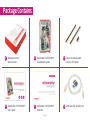
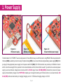
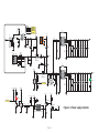
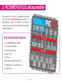
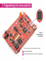
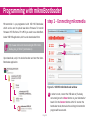
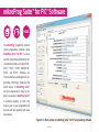
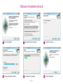
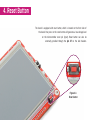
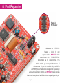
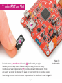
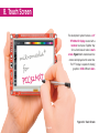
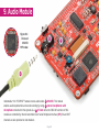
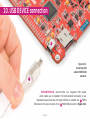
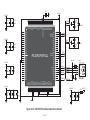
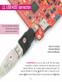
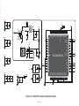
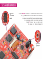
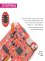
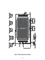
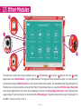
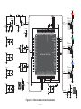
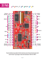
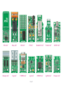
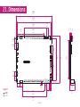
mikromedia+ for PIC32MX7® Amazingly compact, all-on-single-pcb development board carring 4.3’’ TFT Touch Screen and lots of multimedia peripherals, all driven by powerful PIC32MX795F512L microcontroller. TO OUR VALUED CUSTOMERS I want to express my thanks to you for being interested in our products and for having confidence in MikroElektronika. The primary aim of our company is to design and produce high quality electronic products and to constantly improve the performance thereof in order to better suit your needs. Nebojsa Matic General Manager The PIC32® and Windows® logos and product names are trademarks of Microchip Technology® and Microsoft® in the U.S.A. and other countries. Page 2 Table of Contents 6. Port Expander 22 System Specification 4 7. MicroSD Card Slot 24 Package Contains 5 8. Touch Screen 26 1. Power Supply 6 9. Audio Module 28 2. PIC32MX795F512L Microcontroller 8 10. USB DEVICE Connection 30 8 11. USB HOST Connection 32 3. Programming the Microcontroller 9 12. Accelerometer 34 Programming with mikroBootloader 10 13. Flash Memory 36 Introduction to mikromedia+ for PIC32MX7®4 Key Microcontroller Features step 1 – Connecting mikromedia 10 14. RF Transceiver 38 step 2 – Browsing for .HEX file 11 15. Ethernet Transceiver 40 step 3 – Selecting .HEX file 11 16. Buzzer 42 step 4 – Uploading .HEX file 12 17. Other Modules 44 step 5 – Finish upload 13 18. Pads 46 14 19. mikromedia+ for PIC32MX7® SHIELD48 mikroProg suite™ for PIC® Software 16 20. Click boards are plug and play! 50 Software Installation Wizard 17 21. Dimensions 52 4. Reset Button 18 22. What’s next 53 5. Crystal Oscillators a nd 2.048V Reference 20 Programming with mikroProg™ Programmer Page 3 Introduction to mikromedia+ for PIC32MX7® System Specification The mikromedia+ for PIC32MX7® is a compact development system which allows development of devices with multimedia contents. The central part of the system is a 32-bit 100-pin PIC32MX795F512L microcontroller. The mikromedia+ for PIC32MX7® feature lots of on board modules such as stereo power supply Via USB cable (5V DC) or via screw terminals (5 - 12V DC) MP3 codec, 4.3’’ TFT 480x272 touch screen display, port expander, accelerometer, microSD card slot, buzzer, IR receiver, RGB LED diode, PIN photodiode, temperature sensor, 2.4GHz RF transceiver, Ethernet transceiver, 8 Mbit flash memory, Li-Polimer battery charger etc. The board also contains MINI-B USB connector, power screw terminals, 2x5 mikroProg™ connector, two 1x26 connection pads, ON/OFF switch and other. It comes pre-programmed with USB HID bootloader, but can also be programmed with mikroProg™ for PIC®, dsPIC® and PIC32® external programmer. mikromedia is compact and slim, and perfectly fits in the palm of your hand, which makes it a convenient platform for mobile and other multimedia devices. We have also prepared a mikromedia+ SHIELD for PIC32MX7® extension board which enables you to easily expand the functionality of your board. power consumption 65mA with erased MCU (when on-board modules are inactive) board dimensions 119.54 x 78mm (4.71 x 3.07inch) weight ~115g (0.253lbs) Page 4 Package Contains 01 Damage resistant protective box 02 mikromedia+ for PIC32MX7® development system 03 Two 1x26 male headers and one 2x5 header 04 mikromedia+ for PIC32MX7® user’s guide 05 mikromedia+ for PIC32MX7® schematic 06 USB cable and microSD card Page 5 1. Power Supply Figure 1-1: USB power supply Figure 1-2: Battery power supply Figure 1-3: Screw terminals power supply The mikromedia+ for PIC32MX7® board can be powered in three different ways: via USB connector using MINI-B USB cable provided with the board (CN4), via battery connector using Li-Polymer battery (CN5) or via screw terminals using laboratory power supply (CN3). After you plug in the appropriate power supply turn the power switch ON (SW1). The USB connection can provide up to 500mA of current which is more than enough for the operation of all on-board modules and the microcontroller as well. If you decide to use external power supply via screw terminals, voltage levels must be within 5-12V DC range. Power LED ON (GREEN) indicates the presence of power supply. On-board battery charger circuit MCP73832 enables you to charge the battery over USB connection or via screw terminals. LED diode (RED) indicates when battery is charging. Charging current is ~250mA and charging voltage is 4.2V DC. Page 6 VCC-3.3V Q1 USB-PSW 1 4 U6 EN 3 R38 10K 5 VCC-5V R1 3 OC 2 1 2 3 4 5 1 2 3 4 5 CN3 R42 D4 E7 10uF M1 DMP2160UW E8 10uF R46 D5 B340A 10K USB-VBUS 2 3 R51 1M CN5 1 2 3 4 5 VIN PWR-EN R29 100K BAT-VSENSE BAT-VSENSE C72 C79 22uF 1uF 100nF 10nF C140 C141 100pF SW1 JS202011AQN VCC-5V VCC-3.3V Q4 BC846 R61 10K LD1 TPS63060 C73 22uF VCC-3.3V R50 100K R52 12K C77 100nF R53 4K7 C78 C74 C75 C76 C142 C143 22uF 22uF 22uF 1uF 100nF 10nF C144 1 2 3 U12 STAT PROG VSS VBAT VDD 100pF 10pF 4 V_INPUT R105 MCP73832 Charging Current approx. 250mA R104 10K M4 DMG3420U 5 R62 3K9 1K C80 2.2uF Page 7 POWER C145 VCC-5V M3 DMP2160UW R59 1K C81 10uF 10 9 8 7 6 Vbat_IN E12 10uF CHARGE L1 L2 VIN VOUT EN PGND FB PS GND PG VAUX R55 1K R58 10K LD2 R60 C68 22uF L3 1 M2 DMP2160UW R54 1M 10K C67 22uF 1.5uH VCC-3.3V Q3 BC846 C66 10pF U9 VIN BAT-STAT C70 PMEG3010ER R49 1M BAT-STAT R45 10K V_INPUT USB-D_N USB-D_P USB-ID R57 1K VCC-5V R41 100K R43 1K Vbat_IN R56 10K 10 9 8 7 6 C71 100nF C69 22uF R47 1K VCC-3.3V VCC-3.3V L1 L2 VIN VOUT EN PGND FB PS GND PG VAUX TPS63060 D2 B340A 10K FP5 USB MINIB U7 VIN PWR-EN Vusb_IN VBUS DD+ ID GND 1.5uH Vdc C136 100nF D3 PMEG3010ER CN4 L2 Vusb_OUT 1 IN OUT TPS2041B PDTC114EU USB-PSW USB-VBUS USB-D_N USB-D_P USB-ID 2 GND E9 10uF R2 USB-PSW USB-VBUS USB-D_N USB-D_P USB-ID Figure 1-4: Power supply schematic R44 470 2. PIC32MX795F512L microcontroller The mikromedia+ for PIC32MX7® development board comes with the 100-pin PIC32MX795F512L microcontroller. This high-performance 32-bit microcontroller has integrated modules, such as 512K of flash and 128K of RAM easily handling demanding applications. MIPS M4K 32 -bit core - 80MHz, 1. 56 DMIPS/M Hz - 5 Stage Pi peline, 32-b it ALU Trace 32-bit 32 Core HW Registers JTAG Mul/Div Shadow Se t Instruction Data Key microcontroller features - Up to 125 DMIPS Operation (80MHz); - 512K bytes of Flash memory; - 16-bit timers; DMA 8Ch 2-wire Debug USB OTG Bus Matrix Prefetch Buffer Cach e Flash - 128K bytes of RAM memory; - up to 85 I/O pins; PIC32 RAM Interrupt Controller Peripherial 16-bit Parallel Port - 8MHz internal oscillator, 32kHz RTCC, PLL; RTCC - 6xUART, 4xSPI, 5xI2C, 2xCAN, ADC etc., and - Ethernet, USB etc. Page 8 16 Ch 10-bit ADCs I2C (5) GPIO (85) VREG Bus Input Capture (5) UARTs (6) Output Compare PWM(5) 16-bit Timers (5) SPI Analog Comparators (4) (2) 3. Programming the microcontroller Figure 3-1: PIC32MX795F512L microcontroller The microcontroller can be programmed in two ways: 01 Using USB mikroBootloader 02 Using external mikroProg™ for PIC®, dsPIC®, PIC32® programmer Page 9 Programming with mikroBootloader Microcontroller is pre-programmed with USB HID Bootloader, which can be used to upload new device firmware. To transfer firmware .HEX file from a PC to MCU you need to use mikroBootloader USB HID application, which can be downloaded from: http://www.mikroe.com/downloads/get/2031/mikromedia_plus_pic32mx7_bootloader.zip step 1 – Connecting mikromedia 01 02 Upon download, unzip it to desired location and start the mikroBootloader application: Figure 3-2: USB HID mikroBootloader window 01 In order to start, connect the USB cable or (if already connected) press the Reset button on your mikromedia+ board. Click the Connect button within 5s to enter the bootloader mode, otherwise the existing microcontroller program will be executed. Page 10 step 2 – Browsing for .HEX file step 3 – Selecting .HEX file 01 0101 02 Figure 3-3: Browse for HEX Figure 3-4: Selecting HEX 01 Click the Browse for HEX button and from a pop-up window (Figure 3.4) choose the .HEX file that will be uploaded to MCU memory. 01 Select .HEX file from the Open dialog window. 02 Click the Open button. Page 11 step 4 – Uploading .HEX file 01 01 Figure 3-5: Begin uploading Figure 3-6: Progress bar 01 In order to upload .HEX file click the Begin uploading button. 01 .HEX file uploading can be monitored via progress bar. Page 12 step 5 – Finish Upload 01 01 Figure 3-7: Restarting MCU Figure 3-8: mikroBootloader ready to use 01 Click the OK button after uploading is finished. The board will be automatically reset and after 5 seconds your new program will be executed. Page 13 Programming with mikroProg™ Programmer Figure 3-9: mikroProg™ connector The microcontroller can be programmed with external mikroProg™ for PIC®, dsPIC® and PIC32® programmer and mikroProg Suite™ for PIC® software. The external programmer is connected to the development system via 2X5 mikroProg™ connector, Figure 3-9. mikroProg™ is a fast USB 2.0 programmer with hardware Debugger support. It supports IC10®, PIC12®, PIC16®, PIC18®, dsPIC30/33®, PIC24® and PIC32® devices from Microchip®. Outstanding performance, easy operation and elegant design are it’s key features. Page 14 E10 VCC-3.3V VCC-3.3V C113 100nF 100nF U18 VCC-3.3V C114 C115 C116 100nF 100nF 100nF MCLR# VCC-3.3V C117 C124 C125 100nF 1uF 1uF VCC-3.3V C127 C128 C129 1uF 10nF 10nF 10nF RG15 VDD RE5 RE6 RE7 RC1 RC2 RC3 RC4 RG6 RG7 RG8 MCLR RG9 VSS VDD RA0 RE8 RE9 RB5 RB4 RB3 RB2 RB1 RB0 PIC32MX795F512L VSS SOSCO/RC14 SOSCI/RC13 RD0 RD11 RD10 RD9 RD8 RA15 RA14 VSS OSC2/RC15 OSC1/RC12 VDD RA5 RA4 RA3 RA2 D+/RG2 D-/RG3 VUSB VBUS RF8 RF2 RF3 FP4 C133 C134 C135 1uF 100nF 10nF VCC-3.3V VCC-ADC VCC-ADC HDR-AN4/PGC HDR-AN5/PGD 26 27 28 29 30 31 32 33 34 35 36 37 38 39 40 41 42 43 44 45 46 47 48 49 50 C126 1 2 3 4 5 6 7 8 9 10 11 12 13 14 15 16 17 18 19 20 21 22 23 24 25 RE4 RE3 RE2 RG13 RG12 RG14 RE1 RE0 RA7 RA6 RG0 RG1 RF1 RF0 VDD VCAP/VDDCORE RD7 RD6 RD5 RD4 RD13 RD12 RD3 RD2 RD1 C112 100nF RB6 RB7 RA9 RA10 AVDD AVSS RB8 RB9 RB10 RB11 VSS VDD RA1 RF13 RF12 RB12 RB13 RB14 RB15 VSS VDD RD14 RD15 RF4 RF5 C111 100 99 98 97 96 95 94 93 92 91 90 89 88 87 86 85 84 83 82 81 80 79 78 77 76 10uF Figure 3-10: mikroProg™ connection schematic Page 15 75 74 73 72 71 70 69 68 67 66 65 64 63 62 61 60 59 58 57 56 55 54 53 52 51 C109 22pF X5 32.768KHz C110 22pF C107 22pF X4 16MHz C108 22pF VCC-3.3V HDR-AN4/PGC HDR-AN5/PGD MCLR# 1 3 5 7 9 2 4 6 8 10 CN7 mikroProg Suite™ for PIC® Software PIC32 The mikroProg™ programmer requires special programming software called mikroProg Suite™ for PIC®. It can be used for programming all Microchip® microcontroller families, including PIC10®, PIC12®, PIC16®, PIC18®, dsPIC30/33®, PIC24® and PIC32®. Software has intuitive interface and SingleClick™ programming technology. Download the latest version of mikroProg Suite™ and your programmer is ready to program new devices. mikroProg Suite™ is updated regularly, at least four times a year, so your programmer will be more and more powerful with each new release. Figure 3-11: Main window of mikroProg Suite™ for PIC® programming software Page 16 Software Installation Wizard 01 Start Installation 02 Accept EULA and continue 03 Install for all users 04 Choose destination folder 05 Installation in progress 06 Finish installation Page 17 4. Reset Button The board is equipped with reset button, which is located on the front side of the board. One press on the reset button will generate a low voltage level on the microcontroller reset pin (input). Reset button can also be externally provided through the pin 27 on the side headers. Figure 4-1: Reset button VCC-3.3V VCC-3.3V C113 100nF 100nF 100nF E10 T1 RESET C99 100nF U18 VCC-3.3V C116 100nF 100nF VCC-3.3V VCC-3.3V C117 C124 C125 100nF 1uF 1uF C126 C127 C128 C129 1uF 10nF 10nF 10nF VCC-3.3V HDR2 27 28 29 30 31 32 33 34 35 36 37 38 39 40 41 42 43 44 45 46 47 48 49 50 51 52 M1X26 MCLR# RG15 VDD RE5 RE6 RE7 RC1 RC2 RC3 RC4 RG6 RG7 RG8 MCLR RG9 VSS VDD RA0 RE8 RE9 RB5 RB4 RB3 RB2 RB1 RB0 PIC32MX795F512L VSS SOSCO/RC14 SOSCI/RC13 RD0 RD11 RD10 RD9 RD8 RA15 RA14 VSS OSC2/RC15 OSC1/RC12 VDD RA5 RA4 RA3 RA2 D+/RG2 D-/RG3 VUSB VBUS RF8 RF2 RF3 RB6 RB7 RA9 RA10 AVDD AVSS RB8 RB9 RB10 RB11 VSS VDD RA1 RF13 RF12 RB12 RB13 RB14 RB15 VSS VDD RD14 RD15 RF4 RF5 C115 100nF 1 2 3 4 5 6 7 8 9 10 11 12 13 14 15 16 17 18 19 20 21 22 23 24 25 26 27 28 29 30 31 32 33 34 35 36 37 38 39 40 41 42 43 44 45 46 47 48 49 50 C114 VCC-3.3V 10uF 100 99 98 97 96 95 94 93 92 91 90 89 88 87 86 85 84 83 82 81 80 79 78 77 76 C112 RE4 RE3 RE2 RG13 RG12 RG14 RE1 RE0 RA7 RA6 RG0 RG1 RF1 RF0 VDD VCAP/VDDCORE RD7 RD6 RD5 RD4 RD13 RD12 RD3 RD2 RD1 C111 R69 10K Vdc VCC-ADC Figure 4-2: Reset button connection schematic Page 19 75 74 73 72 71 70 69 68 67 66 65 64 63 62 61 60 59 58 57 56 55 54 53 52 51 C109 22pF C110 22pF C107 22pF C108 22pF VCC-ADC X5 32.768KHz X4 16MHz FP4 C133 C134 C135 1uF 100nF 10nF VCC-3.3V 5. Crystal Oscillators and 2.048V Reference The board is equipped with 01 16MHz crystal oscillator (X4) circuit that provides external clock waveform to the microcontroller OSC1 and OSC2 pins. This base frequency is suitable for further clock multipliers and ideal for generation of necessary USB clock, which ensures proper operation of bootloader and your custom USB-based applications. The board also contains 02 32.768kHz crystal 02 03 01 oscillator (X5) which provides external clock for internal RTCC module. Microcontroller ADC requires an accurate source of reference voltage signal. That is why we provide the external 03 voltage reference to the microcontroller VREF pin which is 2.048V. 01 02 03 Figure 5-1: Crystal oscillator and 2.048V reference Page 20 E10 VCC-3.3V VCC-3.3V C112 C113 100nF 100nF 100nF U18 1 2 3 4 5 6 7 8 9 10 11 12 13 14 15 16 17 18 19 20 21 22 23 24 25 VCC-3.3V C114 C115 C116 100nF 100nF 100nF VCC-3.3V C124 C125 100nF 1uF 1uF PIC32MX795F512L VSS SOSCO/RC14 SOSCI/RC13 RD0 RD11 RD10 RD9 RD8 RA15 RA14 VSS OSC2/RC15 OSC1/RC12 VDD RA5 RA4 RA3 RA2 D+/RG2 D-/RG3 VUSB VBUS RF8 RF2 RF3 75 74 73 72 71 70 69 68 67 66 65 64 63 62 61 60 59 58 57 56 55 54 53 52 51 C109 22pF C110 22pF C107 22pF C108 22pF C126 C127 C128 C129 1uF 10nF 10nF 10nF X4 16MHz FP4 C133 C134 C135 1uF 100nF 10nF 26 27 28 29 30 31 32 33 34 35 36 37 38 39 40 41 42 43 44 45 46 47 48 49 50 VCC-3.3V X5 32.768KHz VCC-ADC RB6 RB7 RA9 RA10 AVDD AVSS RB8 RB9 RB10 RB11 VSS VDD RA1 RF13 RF12 RB12 RB13 RB14 RB15 VSS VDD RD14 RD15 RF4 RF5 C117 RG15 VDD RE5 RE6 RE7 RC1 RC2 RC3 RC4 RG6 RG7 RG8 MCLR RG9 VSS VDD RA0 RE8 RE9 RB5 RB4 RB3 RB2 RB1 RB0 RE4 RE3 RE2 RG13 RG12 RG14 RE1 RE0 RA7 RA6 RG0 RG1 RF1 RF0 VDD VCAP/VDDCORE RD7 RD6 RD5 RD4 RD13 RD12 RD3 RD2 RD1 C111 100 99 98 97 96 95 94 93 92 91 90 89 88 87 86 85 84 83 82 81 80 79 78 77 76 10uF VCC-3.3V 1 VCC-ADC 2 C132 10nF C104 100nF C105 1uF Figure 5-2: Crystal oscillators and voltage reference connection schematic Page 21 REF1 MAX6106EUR+ IN GND OUT 3 VCC-3.3V 6. Port Expander Figure 6-1: Port Expander mikromedia+ for PIC32MX7 ® features a 16-bit I/O port expander module MCP23S17 which communicates with PIC32MX795F512L microcontroller via SPI serial interface. This module enables you to expand the number of microcontroller I/O pins with two 8-bit I/O ports (PORTA and PORTB). Each of them consists of registers for input, output and polarity selection. In addition, the MCP23S17 module contains interrupt and reset pins and has 25mA sink/source capability per I/O pin. Page 22 E10 VCC-3.3V VCC-3.3V VCC-3.3V VCC-3.3V C130 100nF VCC-3.3V 100 99 98 97 96 95 94 93 92 91 90 89 88 87 86 85 84 83 82 81 80 79 78 77 76 EXP-GPIO7 EXP-GPIO6 EXP-GPIO5 EXP-GPIO4 EXP-GPIO3 EXP-GPIO2 EXP-GPIO1 EXP-GPIO0 EXP-INT EXP-RST# SPI_MISO VCC-3.3V HDR2 27 28 29 30 31 32 33 34 35 36 37 38 39 40 41 42 43 44 45 46 47 48 49 50 51 52 M1X26 EXP-RST# EXP-PWM0 EXP-PWM1 EXP-PWM2 EXP-PWM3 EXP-GPIO6 EXP-GPIO7 EXP-INT0 EXP-INT1 EXP-INT2 EXP-INT3 EXP-INT RG15 VDD RE5 RE6 RE7 RC1 RC2 RC3 RC4 RG6 RG7 RG8 MCLR RG9 VSS VDD RA0 RE8 RE9 RB5 RB4 RB3 RB2 RB1 RB0 PIC32MX795F512L 75 74 73 72 71 70 69 68 67 66 65 64 63 62 61 60 59 58 57 56 55 54 53 52 51 VSS SOSCO/RC14 SOSCI/RC13 RD0 RD11 RD10 RD9 RD8 RA15 RA14 VSS OSC2/RC15 OSC1/RC12 VDD RA5 RA4 RA3 RA2 D+/RG2 D-/RG3 VUSB VBUS RF8 RF2 RF3 R100 27 SOSCO SOSCI SPI_MOSI R101 27 SPI_SCK C107 22pF OSC2 OSC1 C108 22pF VCC-3.3V OSC2 OSC1 C111 C112 C113 100nF 100nF 100nF C114 C115 C116 100nF 100nF 100nF C117 C124 C125 100nF 1uF 1uF VCC-3.3V RB6 RB7 RA9 RA10 AVDD AVSS RB8 RB9 RB10 RB11 VSS VDD RA1 RF13 RF12 RB12 RB13 RB14 RB15 VSS VDD RD14 RD15 RF4 RF5 HDR1 1 2 3 4 5 6 7 8 9 10 11 12 13 14 15 16 17 18 19 20 21 22 23 24 25 26 M1X26 X5 32.768KHz U18 1 2 3 4 5 6 7 8 9 10 11 12 13 14 15 16 17 18 19 20 21 22 23 24 25 RE4 RE3 RE2 RG13 RG12 RG14 RE1 RE0 RA7 RA6 RG0 RG1 RF1 RF0 VDD VCAP/VDDCORE RD7 RD6 RD5 RD4 RD13 RD12 RD3 RD2 RD1 28 27 26 25 24 23 22 21 20 19 18 17 16 15 MCP23S17 VCC-5V EXP-GPIO0 EXP-GPIO1 EXP-GPIO2 EXP-GPIO3 EXP-GPIO4 EXP-GPIO5 GPA7 GPA6 GPA5 GPA4 GPA3 GPA2 GPA1 GPA0 INTA INTB RESET A2 A1 A0 C110 22pF VCC-ADC VCC-ADC Vdc VCC-3.3V EXP-CS# R102 27 GPB0 GPB1 GPB2 GPB3 GPB4 GPB5 GPB6 GPB7 VDD VSS CS SCK SI SO R99 100K 26 27 28 29 30 31 32 33 34 35 36 37 38 39 40 41 42 43 44 45 46 47 48 49 50 EXP-CS# SPI_SCK SPI_MOSI SPI_MISO 1 2 3 4 5 6 7 8 9 10 11 12 13 14 U11 MCP23S17 EXP-PWM0 EXP-PWM1 EXP-PWM2 EXP-PWM3 EXP-INT0 EXP-INT1 EXP-INT2 EXP-INT3 R98 100K C109 22pF SOSCO SOSCI 10uF FP4 VCC-3.3V C134 C135 C126 C127 C128 C129 1uF 100nF 10nF 1uF 10nF 10nF 10nF Figure 6-2: Port Expander connection schematic Page 23 VCC-3.3V C133 X4 16MHz 7. microSD Card Slot 01 02 Figure 7-1: The board contains 01 microSD card slot for using 02 microSD cards in your projects. microSD Card Slot It enables you to store large amounts of data externally, thus saving microcontroller memory. microSD cards use Serial Peripheral Interface (SPI) for communication with the microcontroller. Ferrite and capacitor are provided to compensate the voltage and current glitch that can occur when pushingin and pushing-out microSD card into the socket. Proper insertion of the microSD card is shown in Figure 7-1. Page 24 C111 C112 C113 100nF 100nF 100nF SD-CD# SD-CS# VCC-3.3V E10 C109 22pF SOSCO SOSCI VCC-3.3V X5 32.768KHz C110 22pF 100 99 98 97 96 95 94 93 92 91 90 89 88 87 86 85 84 83 82 81 80 79 78 77 76 10uF 100nF 100nF VCC-3.3V SPI_MISO C117 C124 C125 100nF 1uF 1uF VCC-3.3V C127 C128 C129 1uF 10nF 10nF 10nF RG15 VDD RE5 RE6 RE7 RC1 RC2 RC3 RC4 RG6 RG7 RG8 MCLR RG9 VSS VDD RA0 RE8 RE9 RB5 RB4 RB3 RB2 RB1 RB0 PIC32MX795F512L VSS SOSCO/RC14 SOSCI/RC13 RD0 RD11 RD10 RD9 RD8 RA15 RA14 VSS OSC2/RC15 OSC1/RC12 VDD RA5 RA4 RA3 RA2 D+/RG2 D-/RG3 VUSB VBUS RF8 RF2 RF3 75 74 73 72 71 70 69 68 67 66 65 64 63 62 61 60 59 58 57 56 55 54 53 52 51 R100 27 SOSCO SOSCI SPI_MOSI R101 27 SPI_SCK OSC2 OSC1 RB6 RB7 RA9 RA10 AVDD AVSS RB8 RB9 RB10 RB11 VSS VDD RA1 RF13 RF12 RB12 RB13 RB14 RB15 VSS VDD RD14 RD15 RF4 RF5 C126 1 2 3 4 5 6 7 8 9 10 11 12 13 14 15 16 17 18 19 20 21 22 23 24 25 VCC-ADC C133 C134 C135 1uF 100nF 10nF VCC-MMC SD-CS# SPI_MOSI SPI_SCK SD-DOUT R81 VCC-ADC Figure 7-2: microSD Card Slot module connection schematic Page 25 CN6 1 2 4 5 6 7 27 SD-CD# CS DIN +3.3V SCK GND DOUT CD VCC-3.3V VCC-MMC FP3 FERRITE VCC-3.3V 26 27 28 29 30 31 32 33 34 35 36 37 38 39 40 41 42 43 44 45 46 47 48 49 50 FP4 X4 16MHz C108 22pF C151 22uF C106 100nF microS D CAR D S LOT 100nF C107 22pF OSC2 OSC1 GND C116 10K 10K C115 RE4 RE3 RE2 RG13 RG12 RG14 RE1 RE0 RA7 RA6 RG0 RG1 RF1 RF0 VDD VCAP/VDDCORE RD7 RD6 RD5 RD4 RD13 RD12 RD3 RD2 RD1 U18 C114 R79 R80 VCC-3.3V 8. Touch Screen The development system features a 4.3‘‘ TFT 480x272 display covered with a resistive touch panel. Together they form a functional unit called a touch screen, Figure 8-1. It enables data to be entered and displayed at the same time. The TFT display is capable of showing graphics in 256K different colors. Figure 8-1: Touch Screen Page 26 75 74 73 72 71 70 69 68 67 66 65 64 63 62 61 60 59 58 57 56 55 54 53 52 51 R95 4K7 SOSCO SOSCI C109 22pF SOSCO SOSCI C110 22pF X5 32.768KHz VCC-3.3V IN OUT 2 C41 2.2uF GND 3 EN ADJ AP7331-ADJ TP_INT# OSC2 OSC1 C107 22pF OSC2 OSC1 C108 22pF TFT-D0 TFT-D1 TFT-D2 TFT-D3 TFT-D4 VCC-1.2V U3 1 5 R10 100K 4 R11 100K E1 10uF R12 100K X4 16MHz R8 I2C_SDA I2C_SCL 22pF C39 220 X1 XTAL_OUT 10MHz C40 22pF LCD-R7 LCD-R6 LCD-R5 LCD-R4 AT043B35-15I-10 16 X15 Y+ 14 Vio 13 X+ TFT-D11 TFT-D12 TFT-D13 TFT-D14 TFT-D15 33 34 35 36 37 38 39 40 41 42 43 44 45 46 47 48 49 50 51 52 53 54 55 56 57 58 59 60 61 62 63 64 LCD-R0 LCD-G7 LCD-G6 LCD-G5 LCD-G4 LCD-PWM LCD-VSYNC LCD-HSYNC LCD-DCLK LCD-R1 VLEDVLED+ GND VDD R0 R1 R2 R3 R4 R5 R6 R7 G0 G1 G2 G3 G4 G5 G6 G7 B0 B1 B2 B3 B4 B5 B6 B7 GND DCLK DISP HSYNC VSYNC DE NC GND X_R Y_B X_L Y_T 12 11 10 9 C3 C4 C5 C6 C7 C8 C9 C10 C11 C12 C13 C14 C15 C16 C17 C18 C19 C20 1uF 1uF 1uF 1uF 1uF 1uF 1uF 1uF 1uF 1uF 1uF 1uF 1uF 1uF 1uF 1uF 1uF 1uF C21 VCC-3.3V C22 C23 C24 C25 C26 C27 C28 C29 100nF 100nF 100nF 100nF 100nF 100nF 100nF 100nF 100nF C30 C31 C32 C33 C34 C35 C36 C37 1 2 3 4 5 6 7 8 9 10 11 12 13 14 15 16 17 18 19 20 21 22 23 24 25 26 27 28 29 30 31 32 33 34 35 36 37 38 39 40 CN1 D1 10uH U1 VIN SW GND EN FB TPS61041 1 2 3 PMEG3010ER DZ1 MMSZ5246B C1 100nF R1 34 R3 0R TP-X_R TP-Y_B TP-X_L TP-Y_T LCD-PWM 4 LCD-DCLK 5 LCD-HSYN C LCD-VSYN C LCD-DE FP1 C2 10uF C111 C112 C113 C114 C115 C116 C117 C124 C125 C126 C127 C128 C129 100nF 100nF 100nF 100nF 100nF 100nF 100nF 1uF 1uF 1uF 10nF 10nF 10nF VCC-ADC VLED+ VLED- LCD-R0 LCD-R1 LCD-R2 LCD-R3 LCD-R4 LCD-R5 LCD-R6 LCD-R7 LCD-G0 LCD-G1 LCD-G2 LCD-G3 LCD-G4 LCD-G5 LCD-G6 LCD-G7 LCD-B0 LCD-B1 LCD-B2 LCD-B3 LCD-B4 LCD-B5 LCD-B6 LCD-B7 L1 Figure 8-2: Touch Screen connection schematic Page 27 FP4 C133 C134 C135 1uF 100nF 10nF C38 100nF 100nF 100nF 100nF 100nF 100nF 100nF 100nF 100nF VCC-3.3V VCC-3.3V VCC-5V C146 2.2nF IN3 STMPE IN2 GND 610 Mode YINT A0 SCLK R5 10K VCC-3.3V SDAT VCC SDI NC J2 1 2 3 4 LCD-B6 LCD-B7 LCD-G0 LCD-G1 LCD-G2 LCD-G3 5 6 7 8 1 2 3 TP-Y_T TP-INT# TP-ADR I2C-SCL LCD-B0 LCD-B1 LCD-B2 LCD-B3 LCD-B4 LCD-B5 U13 I2C-SDA VCC-3.3V R65 10K LCD-R2 LCD-R3 VCC-1.2V C147 2.2nF C149 2.2nF C148 2.2nF VCC-3.3V 96 95 94 93 92 91 90 89 88 87 86 85 84 83 82 81 80 79 78 77 76 75 74 73 72 71 70 69 68 67 66 65 VSS VDDIO VSS VDDD D20 D21 D22 D23 D18 D19 LDATA18 LDATA19 VDDLCD VSS VDDD LDATA0 LDATA1 LDATA2 LDATA3 LDATA4 LDATA5 VDDLCD VSS VDDD LDATA6 LDATA7 LDATA8 LDATA9 LDATA10 LDATA11 VDDLCD VSS SSD1963 R9 100K TFT-D/C# TP-X_R TP-X_L TP-Y_B TFT-CS# VCC-ADC 26 27 28 29 30 31 32 33 34 35 36 37 38 39 40 41 42 43 44 45 46 47 48 49 50 TFT1 XTAL_IN VDDD VSS VSS VDDIO VSS VDDD D0 D1 D2 D3 D4 VDDIO VSS VDDD CLK VDDIO VSS VDDPLL VSSPLL VSS VDDD XTAL_IN VSS XTAL_OUT VDDD VSS VDDLCD LDATA23 LDATA22 LDATA21 LDATA20 VDDD LCD-DE PIC32MX795F512L TFT-D5 TFT-D6 TFT-D7 TFT-D8 TFT-D9 TFT-D10 128 127 126 125 124 123 122 121 120 119 118 117 116 115 114 113 112 111 110 109 108 107 106 105 104 103 102 101 100 99 98 97 TFT-D8 TFT-D9 TFT-D10 TFT-D11 VCAP/VDDCORE TFT-D15 TFT-D14 TFT-RD# TFT-WR# TFT-D13 TFT-D12 VSS SOSCO/RC14 SOSCI/RC13 RD0 RD11 RD10 RD9 RD8 RA15 RA14 VSS OSC2/RC15 OSC1/RC12 VDD RA5 RA4 RA3 RA2 D+/RG2 D-/RG3 VUSB VBUS RF8 RF2 RF3 RB6 RB7 RA9 RA10 AVDD AVSS RB8 RB9 RB10 RB11 VSS VDD RA1 RF13 RF12 RB12 RB13 RB14 RB15 VSS VDD RD14 RD15 RF4 RF5 RG15 VDD RE5 RE6 RE7 RC1 RC2 RC3 RC4 RG6 RG7 RG8 MCLR RG9 VSS VDD RA0 RE8 RE9 RB5 RB4 RB3 RB2 RB1 RB0 R94 4K7 CONF RESET# VDDD VSS VDDIO CS# D/C# E (RD#) R/W# (WR#) VDDD VSS VDDIO D5 D6 D7 D8 D9 D10 VDDD VSS VDDIO D11 D12 D13 D14 D15 VDDD VSS VDDIO D16 D17 VDDIO 1 2 3 4 5 6 7 8 9 10 11 12 13 14 15 16 17 18 19 20 21 22 23 24 25 26 27 28 29 30 31 32 VSS VDDLCD LDATA17 GPIO0 GPIO1 GPIO2 GPIO3 VDDD VSS VDDLCD LFRAME LLINE LSHIFT VDDD VSS VDDLCD LDEN TE PWM GAMAS0 GAMAS1 VDDLCD VSS VDDD VSS VDDLCD LDATA16 LDATA15 LDATA14 LDATA13 LDATA12 VDDD 1 2 3 4 5 6 7 8 9 10 11 12 13 14 15 16 17 18 19 20 21 22 23 24 25 RE4 RE3 RE2 RG13 RG12 RG14 RE1 RE0 RA7 RA6 RG0 RG1 RF1 RF0 VDD VCAP/VDDCORE RD7 RD6 RD5 RD4 RD13 RD12 RD3 RD2 RD1 U18 TFT-D5 TFT-D6 TFT-D7 TFT-RST# VCC-3.3V U2 VCC-3.3V 100 99 98 97 96 95 94 93 92 91 90 89 88 87 86 85 84 83 82 81 80 79 78 77 76 TFT-D4 TFT-D3 TFT-D2 TFT-D1 TFT-D0 10uF TFT-CS# TFT-D/C# TFT-RD# TFT-WR# TFT-RST# VCC-1.2V R7 100K E10 VCC-3.3V VCC-3.3V C96 C97 100nF 100nF 9. Audio Module Figure 9-1: On-board VS1053 MP3 codec 03 01 02 mikromedia+ for PIC32MX7® features stereo audio codec 01 VS1053. This module enables audio reproduction and sound recording by using 02 stereo headphones with microphone connected to the system via a 03 3.5mm connector CN2. All functions of this module are controlled by the microcontroller over Serial Peripheral Interface (SPI). IN and OUT channels are also provided on side headers. Page 28 VCC-1.8V C56 100nF C60 100nF C61 100nF C57 100nF C62 100nF C138 100nF C63 100nF C58 100nF C64 100nF C65 100nF LINE_OUT_L R14 100K 10uF C42 3.3nF E3 R15 470 LINE_OUT_R E10 R16 100K 10uF VCC-3.3V R17 1K C44 MICP GBUF 100nF 1 4 3 RIGHT VCC-1.8V LEFT R19 10 2 48 47 46 45 44 43 42 41 40 39 38 37 R22 10 R26 10K R23 10 R24 10 R25 10 C46 C47 C48 10nF SPI_MISO E4 10uF SPI_SCK SPI_MOSI SPI_MISO MP3-CS# MP3-RST# MP3-DREQ MP3-DCS SPI_MISO SPI_MOSI SPI_SCK R30 470 LN-IN_R 1 2 3 R32 10K MICP MIC/LN-IN_L LN-IN_L J1 C50 1uF LINE_IN_R PIC32MX795F512L VSS SOSCO/RC14 SOSCI/RC13 RD0 RD11 RD10 RD9 RD8 RA15 RA14 VSS OSC2/RC15 OSC1/RC12 VDD RA5 RA4 RA3 RA2 D+/RG2 D-/RG3 VUSB VBUS RF8 RF2 RF3 75 74 73 72 71 70 69 68 67 66 65 64 63 62 61 60 59 58 57 56 55 54 53 52 51 R100 27 SOSCO SOSCI SPI_MOSI R101 27 SPI_SCK OSC0 OSC1 MP3-CS# LINE_IN_L LN-IN_L 10nF VCC-3.3V RG15 VDD RE5 RE6 RE7 RC1 RC2 RC3 RC4 RG6 RG7 RG8 MCLR RG9 VSS VDD RA0 RE8 RE9 RB5 RB4 RB3 RB2 RB1 RB0 R31 470 26 27 28 29 30 31 32 33 34 35 36 37 38 39 40 41 42 43 44 45 46 47 48 49 50 R28 27 10nF CUI_SJ-43514-SMT 10nF VS1053 R21 10 47nF 36 35 34 33 32 31 30 29 28 27 26 25 13 14 15 16 17 18 19 20 21 22 23 24 GPIO MP3-DREQ GPIO4 GND GPIO1 GPIO0 XTEST CVDD3 SO SI SCLK TX RX GPIO5 R20 10 C53 R27 10K MICP/LN1 MICN XRESET DGND0 CVDD0 IOVDD0 CVDD1 DREQ GPIO2 GPIO3 GPIO6 GPIO7 GPIO 1 2 3 4 5 6 7 8 9 10 11 12 XDCS/BSYNC IOVDD1 VC0 DGND1 XTAL0 XTAL1 IOVDD2 DGND2 DGND3 DGND4 XCS CVDD2 MIC/LN-IN_L MICN MP3-RST# C51 1uF VCC-3.3V MP3-DCS R33 10K VCC-ADC MP3-CS# C49 100nF LN2 AGND3 LEFT AVDD2 RCAP AVDD1 GBUF AGND2 AGND1 RIGHT AVDD0 AGND0 U4 1 2 3 4 5 6 7 8 9 10 11 12 13 14 15 16 17 18 19 20 21 22 23 24 25 CN2 RB6 RB7 RA9 RA10 AVDD AVSS RB8 RB9 RB10 RB11 VSS VDD RA1 RF13 RF12 RB12 RB13 RB14 RB15 VSS VDD RD14 RD15 RF4 RF5 VCC-3.3V U18 R18 1K C45 C52 RIGHT LEFT GBUF LN-IN_R 1uF VCC-3.3V VCC-3.3V 10uF 100 99 98 97 96 95 94 93 92 91 90 89 88 87 86 85 84 83 82 81 80 79 78 77 76 C43 3.3nF RE4 RE3 RE2 RG13 RG12 RG14 RE1 RE0 RA7 RA6 RG0 RG1 RF1 RF0 VDD VCAP/VDDCORE RD7 RD6 RD5 RD4 RD13 RD12 RD3 RD2 RD1 E5 10uF 470 MP3-DCS MP3-RST# MP3-DREQ E2 R13 VCC-3.3V R34 1M X2 X5 32.768KHz 12.288MHz C54 22pF VCC-3.3V C59 2.2uF C55 22pF 1 2 3 U5 IN OUT GND EN ADJ AP7331-ADJ 5 4 VCC-1.8V R35 100K R36 R37 27K4 1K E6 10uF X4 16MHz C109 22pF SOSCO SOSCI C110 22pF C107 22pF C108 22pF OSC2 OSC1 HDR2 27 28 29 30 31 32 33 34 35 36 37 38 39 40 41 42 43 44 45 46 47 48 49 50 51 52 M1X26 LINE_OUT_L LINE_OUT_R LINE_IN_L LINE_IN_R VCC-3.3V C111 C112 C113 C114 C115 C116 C117 C124 C125 C126 C127 C128 C129 100nF 100nF 100nF 100nF 100nF 100nF 100nF 1uF 1uF 1uF 10nF 10nF 10nF C133 C134 C135 1uF 100nF 10nF VCC-ADC Vdc Figure 9-2: Audio module connection schematic Page 29 FP4 VCC-3.3V 10. USB DEVICE connection 01 Figure 10-1: Connecting USB cable to MINI-B USB connector 02 PIC32MX795F512L microcontroller has integrated USB module, which enables you to implement USB communication functionality to your mikromedia board. Connection with target USB host is establish over 01 MINI-B USB connector. For proper insertion of the 02 MINI-B USB cable refer to Figure 10-1. Page 30 E10 VCC-3.3V VCC-3.3V C112 C113 100nF 100nF 100nF 1 2 3 4 5 6 7 8 9 10 11 12 13 14 15 16 17 18 19 20 21 22 23 24 25 VCC-3.3V C114 C115 C116 100nF 100nF 100nF VCC-3.3V C124 C125 100nF 1uF 1uF PIC32MX795F512L VSS SOSCO/RC14 SOSCI/RC13 RD0 RD11 RD10 RD9 RD8 RA15 RA14 VSS OSC2/RC15 OSC1/RC12 VDD RA5 RA4 RA3 RA2 D+/RG2 D-/RG3 VUSB VBUS RF8 RF2 RF3 X5 32.768KHz C110 22pF 75 74 73 72 71 70 69 68 67 66 65 64 63 62 61 60 59 58 57 56 55 54 53 52 51 SOSCO SOSCI C107 22pF OSC2 OSC1 X4 16MHz C108 22pF OSC2 OSC1 Vusb_IN CN4 FP5 USB-D_P USB-D_N USB-VBUS USB-ID USB-D_N USB-D_P USB-ID USB-VBUS 1 2 3 4 5 R47 1K VBUS DD+ ID GND USB MINI RB6 RB7 RA9 RA10 AVDD AVSS RB8 RB9 RB10 RB11 VSS VDD RA1 RF13 RF12 RB12 RB13 RB14 RB15 VSS VDD RD14 RD15 RF4 RF5 C117 RG15 VDD RE5 RE6 RE7 RC1 RC2 RC3 RC4 RG6 RG7 RG8 MCLR RG9 VSS VDD RA0 RE8 RE9 RB5 RB4 RB3 RB2 RB1 RB0 C109 22pF SOSCO SOSCI U18 RE4 RE3 RE2 RG13 RG12 RG14 RE1 RE0 RA7 RA6 RG0 RG1 RF1 RF0 VDD VCAP/VDDCORE RD7 RD6 RD5 RD4 RD13 RD12 RD3 RD2 RD1 C111 100 99 98 97 96 95 94 93 92 91 90 89 88 87 86 85 84 83 82 81 80 79 78 77 76 10uF C126 C127 C128 C129 1uF 10nF 10nF 10nF 26 27 28 29 30 31 32 33 34 35 36 37 38 39 40 41 42 43 44 45 46 47 48 49 50 VCC-3.3V VCC-ADC Figure 10-2: USB DEVICE module connection schematic Page 31 VCC-ADC FP4 C133 C134 C135 1uF 100nF 10nF VCC-3.3V 11. USB HOST connection Note: When the device is working in USB HOST mode, it must not be mounted to other USB HOST. 02 Figure 11-1: Connecting USB cable to MINI-B USB connector via USB adapter 01 PIC32MX795F512L can also be used as USB HOST which enables microcontroller to establish connection with the target device (eg. USB keyboard, USB mouse, etc). The board provides necessary power supply to the target via TPS2041B IC. To connect 01 USB HOST cable, it is necessary to use the appropriate 02 MINI-B USB to USB type A adapter. For proper insertion refer to Figure 11-1. Page 32 VCC-3.3V VCC-3.3V 100nF 100nF 4 Q1 USB-PSW 1 U6 EN 5 VCC-5V R1 OC GND IN OUT 100nF 100nF 100nF CN4 1 2 3 4 5 FP5 VCC-3.3V USB MINIB C124 C125 100nF 1uF 1uF U18 Vusb_IN VBUS DD+ ID GND C117 C136 100nF D3 PMEG3010ER 2 PDTC114EU C116 USB-D_N USB-D_P USB-ID R47 1K E7 10uF E8 10uF USB-VBUS USB-PSW VCC-3.3V VCC-ADC C126 C127 C128 C129 1uF 10nF 10nF 10nF FP4 C133 C134 C135 1uF 100nF 10nF C109 22pF SOSCO SOSCI C110 22pF 1 2 3 4 5 6 7 8 9 10 11 12 13 14 15 16 17 18 19 20 21 22 23 24 25 RG15 VDD RE5 RE6 RE7 RC1 RC2 RC3 RC4 RG6 RG7 RG8 MCLR RG9 VSS VDD RA0 RE8 RE9 RB5 RB4 RB3 RB2 RB1 RB0 PIC32MX795F512L VSS SOSCO/RC14 SOSCI/RC13 RD0 RD11 RD10 RD9 RD8 RA15 RA14 VSS OSC2/RC15 OSC1/RC12 VDD RA5 RA4 RA3 RA2 D+/RG2 D-/RG3 VUSB VBUS RF8 RF2 RF3 RB6 RB7 RA9 RA10 AVDD AVSS RB8 RB9 RB10 RB11 VSS VDD RA1 RF13 RF12 RB12 RB13 RB14 RB15 VSS VDD RD14 RD15 RF4 RF5 X5 32.768KHz VCC-3.3V 10uF 1 TPS2041B VCC-3.3V C115 Vusb_OUT 2 E9 10uF R2 C114 E10 3 100 99 98 97 96 95 94 93 92 91 90 89 88 87 86 85 84 83 82 81 80 79 78 77 76 100nF R38 10K RE4 RE3 RE2 RG13 RG12 RG14 RE1 RE0 RA7 RA6 RG0 RG1 RF1 RF0 VDD VCAP/VDDCORE RD7 RD6 RD5 RD4 RD13 RD12 RD3 RD2 RD1 C113 VCC-3.3V X4 16MHz C107 22pF OSC2 OSC1 26 27 28 29 30 31 32 33 34 35 36 37 38 39 40 41 42 43 44 45 46 47 48 49 50 C112 3 C111 C108 22pF VCC-ADC Figure 11-2: USB HOST module connection schematic Page 33 75 74 73 72 71 70 69 68 67 66 65 64 63 62 61 60 59 58 57 56 55 54 53 52 51 SOSCO SOSCI OSC2 OSC1 USB-D_P USB-D_N USB-VBUS USB-ID 12. Accelerometer Figure 12-1: Accelerometer module On board ADXL345 accelerometer is used to measure acceleration in three axis: x, y and z. Most common use is to determine the screen orientation, but there are many other fields of usage. Communication between the accelerometer and the microcontroller is performed through I2C interface. There is an option to select the alternate accel address with jumper J3. Figure 12-2: Jumper J3 VCC-3.3V E10 SCL 1 2 3 4 5 6 7 CS VCC GND Res GND GND VCC VCC-3.3V 100nF I2C_SDA ACCEL-ADR 13 12 11 10 9 8 U18 J3 ADXL345 VCC-3.3V C113 100nF 1 2 3 R66 10K ACCEL-INT# C139 100nF X5 32.768KHz C98 100nF C109 22pF SOSCO SOSCI ACCEL-INT# C110 22pF VCC-3.3V VCC-3.3V C114 C115 C116 C126 C127 C128 C129 100nF 100nF 100nF 1uF 10nF 10nF 10nF C117 C124 C125 C133 C134 C135 100nF 1uF 1uF 1uF 100nF 10nF VCC-ADC VCC-3.3V FP4 X4 16MHz C107 22pF OSC2 OSC1 C108 22pF 1 2 3 4 5 6 7 8 9 10 11 12 13 14 15 16 17 18 19 20 21 22 23 24 25 RG15 VDD RE5 RE6 RE7 RC1 RC2 RC3 RC4 RG6 RG7 RG8 MCLR RG9 VSS VDD RA0 RE8 RE9 RB5 RB4 RB3 RB2 RB1 RB0 PIC32MX795F512L VSS SOSCO/RC14 SOSCI/RC13 RD0 RD11 RD10 RD9 RD8 RA15 RA14 VSS OSC2/RC15 OSC1/RC12 VDD RA5 RA4 RA3 RA2 D+/RG2 D-/RG3 VUSB VBUS RF8 RF2 RF3 RB6 RB7 RA9 RA10 AVDD AVSS RB8 RB9 RB10 RB11 VSS VDD RA1 RF13 RF12 RB12 RB13 RB14 RB15 VSS VDD RD14 RD15 RF4 RF5 100nF VCC-3.3V C112 SDA ADD Res NC INT2 INT1 VCC-3.3V 10uF VCC-3.3V 26 27 28 29 30 31 32 33 34 35 36 37 38 39 40 41 42 43 44 45 46 47 48 49 50 C111 VCC-3.3V 100 99 98 97 96 95 94 93 92 91 90 89 88 87 86 85 84 83 82 81 80 79 78 77 76 14 I2C_SCL U14 RE4 RE3 RE2 RG13 RG12 RG14 RE1 RE0 RA7 RA6 RG0 RG1 RF1 RF0 VDD VCAP/VDDCORE RD7 RD6 RD5 RD4 RD13 RD12 RD3 RD2 RD1 VCC-3.3V VCC-ADC Figure 12-3: Accelerometer connection schematic Page 35 R94 4K7 75 74 73 72 71 70 69 68 67 66 65 64 63 62 61 60 59 58 57 56 55 54 53 52 51 R95 4K7 SOSCO SOSCI OSC2 OSC1 I2C_SDA I2C_SCL 13. Flash Memory Since multimedia applications are getting increasingly demanding, it is necessary to provide additional memory space for storing more data. The flash memory module enables the microcontroller to use additional 8Mbit flash memory. It is connected to the microcontroller via the Serial Peripheral Interface (SPI). Figure 13-1: Flash memory module Page 36Page 36 E10 VCC-3.3V VCC-3.3V U18 C123 FLASH-CS# SPI_MISO VCC-3.3V C111 C112 C113 100nF 100nF 100nF VCC-3.3V U19 1 2 3 4 R68 27 CS SDO WP GND 100nF VCC HOLD SCK SDI 8 7 6 5 SPI_SCK SPI_MOSI M25P80 SPI_MISO VCC-3.3V C115 C116 C126 C127 C128 C129 100nF 100nF 100nF 1uF 10nF 10nF 10nF C134 C135 100nF 10nF C124 C125 100nF 1uF 1uF 1uF FP4 SOSCO SOSCI C110 22pF VSS SOSCO/RC14 SOSCI/RC13 RD0 RD11 RD10 RD9 RD8 RA15 RA14 VSS OSC2/RC15 OSC1/RC12 VDD RA5 RA4 RA3 RA2 D+/RG2 D-/RG3 VUSB VBUS RF8 RF2 RF3 VCC-3.3V X4 16MHz C107 22pF OSC2 OSC1 26 27 28 29 30 31 32 33 34 35 36 37 38 39 40 41 42 43 44 45 46 47 48 49 50 C117 C133 C109 22pF PIC32MX795F512L C108 22pF FLASH-CS# VCC-ADC VCC-3.3V X5 32.768KHz RG15 VDD RE5 RE6 RE7 RC1 RC2 RC3 RC4 RG6 RG7 RG8 MCLR RG9 VSS VDD RA0 RE8 RE9 RB5 RB4 RB3 RB2 RB1 RB0 RB6 RB7 RA9 RA10 AVDD AVSS RB8 RB9 RB10 RB11 VSS VDD RA1 RF13 RF12 RB12 RB13 RB14 RB15 VSS VDD RD14 RD15 RF4 RF5 C114 1 2 3 4 5 6 7 8 9 10 11 12 13 14 15 16 17 18 19 20 21 22 23 24 25 VCC-ADC R67 10K RE4 RE3 RE2 RG13 RG12 RG14 RE1 RE0 RA7 RA6 RG0 RG1 RF1 RF0 VDD VCAP/VDDCORE RD7 RD6 RD5 RD4 RD13 RD12 RD3 RD2 RD1 VCC-3.3V 100 99 98 97 96 95 94 93 92 91 90 89 88 87 86 85 84 83 82 81 80 79 78 77 76 10uF Figure 13-2: Flash memory module connection schematic Page 37 75 74 73 72 71 70 69 68 67 66 65 64 63 62 61 60 59 58 57 56 55 54 53 52 51 R100 27 SOSCO SOSCI SPI_MOSI R101 27 SPI_SCK OSC2 OSC1 14. RF Transceiver Figure 14-1: RF transceiver antenna Figure 14-2: RF transceiver module mikromedia+ for PIC32MX7® board features RF transceiver chip with 2.4GHz chip antenna. It is suitable for wireless operation in the world wide ISM frequency band at 2.400 - 2.4835GHz with air data rate up to 2Mbps. RF transceiver module is connected to the microcontroller via the Serial Peripheral Interface (SPI). This RF transceiver module is widely used for wireless PC peripherals, remote controllers, VoIP headsets, game controllers, sensors, home and commercial automation, active RFID, toys and many more. Page 38 E10 VCC-3.3V 100 99 98 97 96 95 94 93 92 91 90 89 88 87 86 85 84 83 82 81 80 79 78 77 76 10uF 1 2 3 4 5 VDD CE VSS CSN nRF24L01P ANT2 SCK ANT1 MOSI VDD_PA MISO 15 14 13 12 11 3.9nH 1.5pF L5 8.2nH SPI_MISO C84 N.M. L6 2.7nH 6 7 8 9 10 R63 10K C92 22pF R64 1M VCC-3.3V C85 2.2nF RF-INT# VCC-RF C91 22pF FP2 FERRITE C88 100nF C89 100nF C109 22pF X5 32.768KHz C90 100nF VCC-ADC FP4 C133 C134 C135 1uF 100nF 10nF SOSCO SOSCI C110 22pF VCC-3.3V VSS SOSCO/RC14 SOSCI/RC13 RD0 RD11 RD10 RD9 RD8 RA15 RA14 VSS OSC2/RC15 OSC1/RC12 VDD RA5 RA4 RA3 RA2 D+/RG2 D-/RG3 VUSB VBUS RF8 RF2 RF3 26 27 28 29 30 31 32 33 34 35 36 37 38 39 40 41 42 43 44 45 46 47 48 49 50 C87 10uF C86 4.7pF X3 16MHz PIC32MX795F512L X4 16MHz C107 22pF OSC2 OSC1 C108 22pF VCC-ADC RF-INT# RG15 VDD RE5 RE6 RE7 RC1 RC2 RC3 RC4 RG6 RG7 RG8 MCLR RG9 VSS VDD RA0 RE8 RE9 RB5 RB4 RB3 RB2 RB1 RB0 RE4 RE3 RE2 RG13 RG12 RG14 RE1 RE0 RA7 RA6 RG0 RG1 RF1 RF0 VDD VCAP/VDDCORE RD7 RD6 RD5 RD4 RD13 RD12 RD3 RD2 RD1 C83 L4 IRQ VDD VSS XC2 XC1 R88 27 A1 Rufa_2.4GHz_LEFT 1 2 3 4 5 6 7 8 9 10 11 12 13 14 15 16 17 18 19 20 21 22 23 24 25 VCC-3.3V C111 C112 C113 C114 C115 C116 C117 C124 C125 C126 C127 C128 C129 100nF 100nF 100nF 100nF 100nF 100nF 100nF 1uF 1uF 1uF 10nF 10nF 10nF Figure 14-3: RF transceiver module connection schematic Page 39 RF-CE RF-CE RF-CS# SPI_SCK SPI_MOSI SPI_MISO U8 20 19 18 17 16 R48 10K VSS DVDD VDD VSS IREF R6 10K U18 VCC-RF R4 22K RB6 RB7 RA9 RA10 AVDD AVSS RB8 RB9 RB10 RB11 VSS VDD RA1 RF13 RF12 RB12 RB13 RB14 RB15 VSS VDD RD14 RD15 RF4 RF5 C82 33nF 75 74 73 72 71 70 69 68 67 66 65 64 63 62 61 60 59 58 57 56 55 54 53 52 51 R100 27 SOSCO SOSCI SPI_MOSI R101 27 SPI_SCK OSC2 OSC1 RF-CS# 14. Ethernet 15. Eternet Transceiver Transceiver Figure 15-1: Ethernet transceiver module The development system features an Ethernet transceiver module ideal for local area networking (LAN). Communication over Ethernet is based on data packets called frames. Each frame contains source and destination addresses and error-checking data so that damaged data can be detected and re-transmitted. If you want to establish connection with computer, router or other devices you need to use standard RJ-45 connector which is provided on mikromedia+ SHIELD for PIC32MX7®. Communication lines are also provided over side headers. Page 40 VCC-ETH LAN-RX_P LAN-RX_N LAN-TX_P LAN-TX_N R2 12K1 FP6 C153 100nF E10 10uF R89 220 C119 22pF 1M C120 C121 22pF 2.2uF C122 100nF GND U18 18 17 16 15 14 13 27 27 27 R86 10K R39 R82 R83 LAN-TXD1 LAN-TXD0 LAN-TXEN LAN-RST# LAN-CLKO LAN-MDC LAN-RXER VCC-ETH LAN-CRS_DV 27 R87 220 Rbias RXP RXN TXP TXN VDD1A 25MHz R85 ACTIVE TXD1 TXD0 TXEN nRST REFCLKO MDC LAN8720A RXD1 RXD0 VDDIO RXER CRS_DV MDIO X6 LD6 LINK U10 7 8 9 10 11 12 LD5 LAN-CLKO R91 R92 R90 1.5K FP4 VCC-3.3V LAN-RXD1 LAN-RXD0 VCC-ADC C133 C134 C135 1uF 100nF 10nF C111 C112 C113 C114 C115 C116 C117 100nF 100nF 100nF 100nF 100nF 100nF 100nF LAN-RXER LAN-CRS_DV R93 LAN-MDIO LAN-RST# LAN-RXD0 LAN-RXD1 X5 32.768KHz VCC-3.3V C124 C125 C126 C127 C128 C129 1uF 1uF 1uF 10nF 10nF 10nF X4 16MHz C109 22pF SOSCO SOSCI C110 22pF C107 22pF RG15 VDD RE5 RE6 RE7 RC1 RC2 RC3 RC4 RG6 RG7 RG8 MCLR RG9 VSS VDD RA0 RE8 RE9 RB5 RB4 RB3 RB2 RB1 RB0 PIC32MX795F512L VSS SOSCO/RC14 SOSCI/RC13 RD0 RD11 RD10 RD9 RD8 RA15 RA14 VSS OSC2/RC15 OSC1/RC12 VDD RA5 RA4 RA3 RA2 D+/RG2 D-/RG3 VUSB VBUS RF8 RF2 RF3 75 74 73 72 71 70 69 68 67 66 65 64 63 62 61 60 59 58 57 56 55 54 53 52 51 SOSCO SOSCI LAN-MDC LAN-MDIO LAN-TXEN VCC-5V OSC2 OSC1 RB6 RB7 RA9 RA10 AVDD AVSS RB8 RB9 RB10 RB11 VSS VDD RA1 RF13 RF12 RB12 RB13 RB14 RB15 VSS VDD RD14 RD15 RF4 RF5 VCC-3.3V 1 2 3 4 5 6 7 8 9 10 11 12 13 14 15 16 17 18 19 20 21 22 23 24 25 26 27 28 29 30 31 32 33 34 35 36 37 38 39 40 41 42 43 44 45 46 47 48 49 50 R84 10K VDD2A LED2 LED1 XTAL2 XTAL1 VDDCR 27 27 1 2 3 4 5 6 LAN-LED2 LAN-LED1 VCC-3.3V VCC-ETH VCC-ADC OSC2 OSC1 C108 22pF Figure 15-2: Ethernet transceiver module schematic Page 41 LAN-TXD0 LAN-TXD1 C131 100nF 100 99 98 97 96 95 94 93 92 91 90 89 88 87 86 85 84 83 82 81 80 79 78 77 76 C118 100nF 24 23 22 21 20 19 E11 10uF RE4 RE3 RE2 RG13 RG12 RG14 RE1 RE0 RA7 RA6 RG0 RG1 RF1 RF0 VDD VCAP/VDDCORE RD7 RD6 RD5 RD4 RD13 RD12 RD3 RD2 RD1 VCC-3.3V LAN-TX_N LAN-TX_P LAN-RX_N LAN-RX_P VCC-3.3V HDR1 1 2 3 4 5 6 7 8 9 10 11 12 13 14 15 16 17 18 19 20 21 22 23 24 25 26 M1X26 16. Buzzer The board is also equipped with piezo buzzer. It is an electric component which can be used to create sound when is provided with electrical signal. This is usually a PWM signal coming from a microcontroller pin. Frequency of the signal determines the pitch of the sound and duty cycle of the signal can be used to increase or decrease the volume. Figure 16-1: Buzzer module E10 VCC-3.3V VCC-3.3V C111 C112 C113 100nF 100nF 100nF 100 99 98 97 96 95 94 93 92 91 90 89 88 87 86 85 84 83 82 81 80 79 78 77 76 10uF C115 C116 100nF 100nF 100nF VCC-3.3V C117 C124 C125 100nF 1uF 1uF C127 C128 C129 1uF 10nF 10nF 10nF 26 27 28 29 30 31 32 33 34 35 36 37 38 39 40 41 42 43 44 45 46 47 48 49 50 C126 75 74 73 72 71 70 69 68 67 66 65 64 63 62 61 60 59 58 57 56 55 54 53 52 51 FP4 C133 C134 C135 1uF 100nF 10nF VCC-3.3V C110 22pF C107 22pF C118 22pF X5 32.768KHz X4 16MHz VCC-5V R74 1K Q8 PDTC114EU BUZZER PZ1 SPT-1325A R1 R2 VCC-ADC BUZZER VCC-ADC C109 22pF RB6 RB7 RA9 RA10 AVDD AVSS RB8 RB9 RB10 RB11 VSS VDD RA1 RF13 RF12 RB12 RB13 RB14 RB15 VSS VDD RD14 RD15 RF4 RF5 VCC-3.3V PIC32MX795F512L VSS SOSCO/RC14 SOSCI/RC13 RD0 RD11 RD10 RD9 RD8 RA15 RA14 VSS OSC2/RC15 OSC1/RC12 VDD RA5 RA4 RA3 RA2 D+/RG2 D-/RG3 VUSB VBUS RF8 RF2 RF3 Figure 16-2: Buzzer module connection schematic Page 43 2 C114 RG15 VDD RE5 RE6 RE7 RC1 RC2 RC3 RC4 RG6 RG7 RG8 MCLR RG9 VSS VDD RA0 RE8 RE9 RB5 RB4 RB3 RB2 RB1 RB0 3 VCC-3.3V RE4 RE3 RE2 RG13 RG12 RG14 RE1 RE0 RA7 RA6 RG0 RG1 RF1 RF0 VDD VCAP/VDDCORE RD7 RD6 RD5 RD4 RD13 RD12 RD3 RD2 RD1 U18 1 2 3 4 5 6 7 8 9 10 11 12 13 14 15 16 17 18 19 20 21 22 23 24 25 17. Other Modules 03 02 04 01 The board also contains other useful peripherals such as 01 PIN photodiode, 02 IR receiver, 03 RGB led diode and 04 analog temperature sensor. PIN photodiode is a type of photo detector. It has high sensitivity and response speed. It is connected to the microcontroller analog pin RB8. IR receiver is used in infrared remote control systems. The demodulated output signal obtained from IR module can be directly decoded by a microcontroller. Many of standard data formats are supported. RGB (Red, Green, Blue) diode can be used as a light indicator. Each color is driven separately by transistor. The analog temperature sensor converts temperature to analog voltage. It is directly connected to the microcontroller RB9 analog pin. Temperature measurement range of mikromedia+ for PIC32MX7® board is from -20° C to 70° C. Page 44 VCC-5V VCC-3.3V 6 4 R40 U17A LM358 150K 7 5 AN-PD C150 100nF U18 C113 100nF 100nF X5 32.768KHz VCC-3.3V C114 C115 C116 100nF 100nF 100nF X4 16MHz C117 C124 C125 100nF 1uF 1uF SOSCO SOSCI C110 22pF IR-RX C107 22pF OSC2 OSC1 C108 22pF RG15 VDD RE5 RE6 RE7 RC1 RC2 RC3 RC4 RG6 RG7 RG8 MCLR RG9 VSS VDD RA0 RE8 RE9 RB5 RB4 RB3 RB2 RB1 RB0 PIC32MX795F512L VCC-5V VSS SOSCO/RC14 SOSCI/RC13 RD0 RD11 RD10 RD9 RD8 RA15 RA14 VSS OSC2/RC15 OSC1/RC12 VDD RA5 RA4 RA3 RA2 D+/RG2 D-/RG3 VUSB VBUS RF8 RF2 RF3 75 74 73 72 71 70 69 68 67 66 65 64 63 62 61 60 59 58 57 56 55 54 53 52 51 SOSCO SOSCI LD3 R72 3K3 Q6 PDTC114EU 1 LED G R1 R2 OSC2 OSC1 VCC-5V LD3 R73 2K2 Q7 PDTC114EU 1 LED B RB6 RB7 RA9 RA10 AVDD AVSS RB8 RB9 RB10 RB11 VSS VDD RA1 RF13 RF12 RB12 RB13 RB14 RB15 VSS VDD RD14 RD15 RF4 RF5 VCC-3.3V C109 22pF 1 2 3 4 5 6 7 8 9 10 11 12 13 14 15 16 17 18 19 20 21 22 23 24 25 R1 R2 26 27 28 29 30 31 32 33 34 35 36 37 38 39 40 41 42 43 44 45 46 47 48 49 50 C112 R2 10uF VCC-3.3V C103 100nF 100nF R1 VCC-3.3V VCC-3.3V C111 1 LED R E10 U17B LM358 100 99 98 97 96 95 94 93 92 91 90 89 88 87 86 85 84 83 82 81 80 79 78 77 76 3 LD4 PD15 1 RE4 RE3 RE2 RG13 RG12 RG14 RE1 RE0 RA7 RA6 RG0 RG1 RF1 RF0 VDD VCAP/VDDCORE RD7 RD6 RD5 RD4 RD13 RD12 RD3 RD2 RD1 8 2 LD3 R71 2K2 Q5 PDTC114EU 3 100K 2 27K4 3 1M 2 R76 3 R77 LED-B LED-G LED-R R78 2 VCC-3.3V C127 C128 C129 1uF 10nF 10nF 10nF TSOP6238 IR-RX C100 4.7uF VCC-ADC AN-PD AN-TEMP C126 4 3 2 1 VCC-ADC U16 VCC-3.3V FP4 C133 C134 C135 1uF 100nF 10nF VCC-3.3V VCC-3.3V 1 AN-TEMP C101 100nF Figure 17-1: Other modules connection schematic Page 45 R75 100 C102 100nF 2 U15 VDD GND VOUT MCP9700A 3 18. Pads 5V power Ref. Ground Analog lines GPIO CAN lines SPI1 lines ETH-TX ETH-RX 3.3V power Ref. Ground 5V GND RB11 RB12 RB1 RB0 RB6 RB7 GPA0 GPA1 GPA2 GPA3 GPA4 GPA5 RC3 RC2 RD9 RD10 RC4 RD0 N P N P 3.3V GND PWM Interrupt I2C UART 1. 2. 3. 4. 5. 6. 7. 8. 9. 10. 11. 12. 13. 14. 15. 16. 17. 18. 19. 20. 21. 22. 23. 24. 25. 26. Analog lines SPI CAN 27. 28. 29. 30. 31. 32. 33. 34. 35. 36. 37. 38. 39. 40. 41. 42. 43. 44. 45. 46. 47. 48. 49. 50. 51. 52. RST 3.3V L R L R GPB0 GPB1 GPB2 GPB3 GPA6 GPA7 GPB4 GPB5 GPB6 GPB7 RA2 RA3 RF2 RF8 RF4 RF5 NC NC GND VDC Reset pin 3.3V pwr. Audio out Audio in PWM Lines GPIO Interrupt Lines I2C2 Lines UART1 Lines UART2 Lines Ref. Ground 5-12V Input Many microcontroller pins are available for further connectivity via two 1x26 rows of connection pads on both sides of the board. They are designed to match with the mikromedia+ SHIELD for PIC32MX7® Page 46 VCC-5V VCC-3.3V VCC-3.3V C115 C116 100nF 100nF 100nF VCC-3.3V C117 C124 C125 100nF 1uF 1uF VCC-3.3V C126 C127 C128 C129 1uF 10nF 10nF 10nF VCC-ADC FP4 C133 C134 C135 1uF 100nF 10nF VCC-3.3V U18 HDR-CAN_TX HDR-CAN_RX HDR-SPI_MISO MCLR# Vdc HDR-AN2 HDR-AN3 SOSCO SOSCI 1 2 3 4 5 6 7 8 9 10 11 12 13 14 15 16 17 18 19 20 21 22 23 24 25 RG15 VDD RE5 RE6 RE7 RC1 RC2 RC3 RC4 RG6 RG7 RG8 MCLR RG9 VSS VDD RA0 RE8 RE9 RB5 RB4 RB3 RB2 RB1 RB0 PIC32MX795F512L VSS SOSCO/RC14 SOSCI/RC13 RD0 RD11 RD10 RD9 RD8 RA15 RA14 VSS OSC2/RC15 OSC1/RC12 VDD RA5 RA4 RA3 RA2 D+/RG2 D-/RG3 VUSB VBUS RF8 RF2 RF3 R94 4K7 75 74 73 72 71 70 69 68 67 66 65 64 63 62 61 60 59 58 57 56 55 54 53 52 51 R95 4K7 R100 27 R101 27 SOSCO SOSCI HDR-SPI_MOSI HDR-SPI_SCK HDR-SPI_SS VCC-3.3V OSC2 OSC1 HDR-I2C2_SDA HDR-I2C2_SCL HDR-UART1_TX HDR-UART1_RX HDR-LN_OUT_L HDR-LN_OUT_R HDR-LN_IN_L HDR-LN_IN_R HDR-ETH_TX_N HDR-ETH_TX_P HDR-ETH_RX_N HDR-ETH_RX_P C110 22pF HDR-GPIO7 HDR-GPIO6 X4 16MHz C107 22pF OSC2 OSC1 C108 22pF Figure 18-1: Connecting pads schematic Page 47 MP3 LINE-OUT_L LINE-OUT_R LINE-IN_L LINE-IN_R ETHERNET ETH_TX_N ETH_TX_P ETH_RX_N ETH_RX_P PORT EXPANDER 26 27 28 29 30 31 32 33 34 35 36 37 38 39 40 41 42 43 44 45 46 47 48 49 50 X5 32.768KHz C109 22pF VCC-3.3V 10uF HDR-UART2_RX HDR-UART2_TX C114 E10 HDR-AN1 100nF HDR-AN0 100nF VCC-ADC 100nF MCLR# HDR-LN_OUT_L HDR-LN_OUT_R HDR-LN_IN_L HDR-LN_IN_R HDR-PWM0 HDR-PWM1 HDR-PWM2 HDR-PWM3 HDR-GPIO6 HDR-GPIO7 HDR-INT0 HDR-INT1 HDR-INT2 HDR-INT3 HDR-I2C2_SCL HDR-I2C2_SDA HDR-UART1_RX HDR-UART1_TX HDR-UART2_RX HDR-UART2_TX 100 99 98 97 96 95 94 93 92 91 90 89 88 87 86 85 84 83 82 81 80 79 78 77 76 C113 RE4 RE3 RE2 RG13 RG12 RG14 RE1 RE0 RA7 RA6 RG0 RG1 RF1 RF0 VDD VCAP/VDDCORE RD7 RD6 RD5 RD4 RD13 RD12 RD3 RD2 RD1 C112 HDR-AN4/PGC HDR-AN5/PGD C111 RB6 RB7 RA9 RA10 AVDD AVSS RB8 RB9 RB10 RB11 VSS VDD RA1 RF13 RF12 RB12 RB13 RB14 RB15 VSS VDD RD14 RD15 RF4 RF5 HDR2 27 28 29 30 31 32 33 34 35 36 37 38 39 40 41 42 43 44 45 46 47 48 49 50 51 52 M1X26 VCC-3.3V HDR1 1 2 3 4 5 6 7 8 9 10 11 12 13 14 15 16 17 18 19 20 21 22 23 24 25 26 M1X26 HDR-AN0 HDR-AN1 HDR-AN2 HDR-AN3 HDR-AN4 HDR-AN5 HDR-GPIO0 HDR-GPIO1 HDR-GPIO2 HDR-GPIO3 HDR-GPIO4 HDR-GPIO5 HDR-CAN_RX HDR-CAN_TX HDR-SPI_SS HDR-SPI_SCK HDR-SPI_MISO HDR-SPI_MOSI HDR-ETH_TX_N HDR-ETH_TX_P HDR-ETH_RX_N HDR-ETH_RX_P HDR-GPIO5 HDR-GPIO4 HDR-GPIO3 HDR-GPIO2 HDR-GPIO1 HDR-GPIO0 HDR-PWM0 HDR-PWM1 HDR-PWM2 HDR-PWM3 HDR-INT0 HDR-INT1 HDR-INT2 HDR-INT3 GPIO7 GPIO6 GPIO5 GPIO4 GPIO3 GPIO2 GPIO1 GPIO0 PWM0 PWM1 PWM2 PWM3 INT0 INT1 INT2 INT3 19. mikromedia+ SHIELD for PIC32MX7® 02 01 07 04 01 03 We have also made an extension board pin-compatible with your mikromedia+ board, which enables you to easily expand your basic board functionality. It is called mikromedia+ SHIELD for PIC32MX7®. The shield contains: 01 FTDI USB-UART chip 05 05 05 05 02 USB MINI-B connector 03 CAN transceiver 04 Screw terminals 05 mikroBUS sockets 06 Power supply screw terminals 07 Side connection pads 08 GNDs 09 08 07 08 06 Figure 19-1: mikromedia+ SHIELD for PIC32MX7® * * not provided in the package Page 48 09 Ethernet connector VCC-3.3V RB11/AN1 RB6/RST1 RB7/CS1 RD10/SPI-SCK RC4/SPI-MISO RD0/SPI-MOSI VCC-5V AN RST CS SCK MISO MOSI 3.3V GND 1 VCC-3.3V RB12/AN2 GPA0/RST2 GPA1/CS2 RD10/SPI-SCK RC4/SPI-MISO RD0/SPI-MOSI GPB0/PWM1 GPB4/INT1 RF4/UART-RX RF5/UART-TX RA2/I2C-SCL RA3/I2C-SDA PWM INT RX TX SCL SDA 5V GND VCC-5V VCC-5V AN RST CS SCK MISO MOSI 3.3V GND 2 VCC-3.3V GPB1/PWM2 GPB5/INT2 RF4/UART-RX RF5/UART-TX RA2/I2C-SCL RA3/I2C-SDA PWM INT RX TX SCL SDA 5V GND VCC-5V RB1/AN3 GPA2/RST3 RD9/CS3 RD10/SPI-SCK RC4/SPI-MISO RD0/SPI-MOSI AN RST CS SCK MISO MOSI 3.3V GND Vinput VCC-3.3V VCC-3.3V HDR2 1 2 3 4 5 6 7 8 9 10 11 12 13 14 15 16 17 18 19 20 21 22 23 24 25 26 RC3/CAN-RX RC2/CAN-TX RD9/CS3 RD10/SPI-SCK RC4/SPI-MISO RD0/SPI-MOSI LAN-TX_N LAN-TX_P LAN-RX_N LAN-RX_P RB0/AN4 GPA6/RST4 GPA7/CS4 RD10/SPI-SCK RC4/SPI-MISO RD0/SPI-MOSI GPB2/PWM3 GPB6/INT3 RF4/UART-RX RF5/UART-TX RA2/I2C-SCL RA3/I2C-SDA PWM INT RX TX SCL SDA 5V GND VCC-5V AN RST CS SCK MISO MOSI 3.3V GND 4 GPB3/PWM4 GPB7/INT4 RF4/UART-RX RF5/UART-TX RA2/I2C-SCL RA3/I2C-SDA PWM INT RX TX SCL SDA 5V GND VCC-3.3V HDR1 RB11/AN1 RB12/AN2 RB1/AN3 RB0/AN4 RB6/RST1 RB7/CS1 GPA0/RST2 GPA1/CS2 GPA2/RST3 3 VCC-3.3V 27 28 29 30 31 32 33 34 35 36 37 38 39 40 41 42 43 44 45 46 47 48 49 50 51 52 VCC-5V C9 100nF VCC-5V C10 100nF E1 10uF VCC-3.3V GPB0/PWM1 GPB1/PWM2 GPB2/PWM3 GPB3/PWM4 GPA6/RST4 GPA7/CS4 GPB4/INT1 GPB5/INT2 GPB6/INT3 GPB7/INT4 RA2/I2C-SCL RA3/I2C-SDA RF2/FTDI-RX RF8/FTDI-TX RF4/UART-RX RF5/UART-TX RF2/FTDI-RX RF8/FTDI-TX VCC-5V 1 2 3 4 5 6 7 8 9 10 11 12 13 14 U2 TXD OSCO DTR# OSCI RTS# TEST VCCIO AGND RXD NC RI# CBUS0 GND CBUS1 FT232RL NC GND DSR# VCC DCD# RESET# CTS# GND CBUS4 3V3OUT CBUS2 USBDM CBUS3 USBDP 28 27 26 25 24 23 22 21 20 19 18 17 16 15 VCC-3.3V VCC-3.3V R6 2K2 R7 4K7 RX-LED TX-LED RX TX LD1 LD2 Vinput D2 PMEG3010ER 1 2 3 4 5 R8 10K FTDI-D_N FTDI-D_P C11 100nF CN3 VBUS DD+ ID GND USB MINIB R9 10K R10 10K VCC-3.3V FP2 VCC-3.3V C12 22uF C13 22uF C14 22uF C2 100nF C3 100nF C4 22uF C5 22uF RC2/CAN-TX RC3/CAN-RX C6 22uF C1 100nF 1 2 3 4 TXD VSS VDD RXD Rs CANH CANL Vref SN65HVD230 8 7 6 5 J5B R11 CANH 100 Figure 19-2: mikromedia+ SHIELD for PIC32MX7® schematic Page 49 R4 51 A2 CT R1 10 RD- R5 51 LAN-RX_N RJ45 C7 10nF CANL LAN-RX_P RD+ CN5 CN2 R3 51 LAN-TX_N TD- CANH CANL A1 FP1 FERRITE B340A LAN-TX_P R2 51 TD+ CT K1 CN1 D1 Vinput U1 K2 CN6 VCC-3.3V CN7 C8 10nF 20. Click boards are plug and play! So far, MikroElektronika has released more than 60 mikroBUS™ compatible click Boards™. On average, one click board is released per week. Our intention is to enable you to easily expand with as many add-on boards as possible, so you will be able to easily expand the functionality of your development board.Each click board™ comes with a set of working example codes. Please, check the list of currently available boards on the following link: http://www.mikroe.com/click/ BUZZ click™ Proximity click™ Compass click™ EVE click™ Fiber Opt click™ GPS2 click™ GSM2 click™ ccRF click™ USB UART click™ Current click™ Dali click™ Page 50 RFid click™ Relay click™ 8X8 click™ BarGraph click™ 7seg click™ THERMO click™ FM click™ Gyro click™ Page 51 Bluetooth2 click™ Thunder click™ USB SPI click™ EEPROM click™ LightHz click™ Pressure click™ 21. Dimensions 119.54 4706 111.54 4391 7.77 306 72.78 2865 5 1.6 4 197 63 157 63.5 2600 9.2 362 24.2 946 7.99 314.5 67.31 2650 78 3071 44.3 1744 70 2756 14.7 579 10.16 400 6.8 268 8.38 330 Legend mm mils 8.64 340 2.54 100 9 354 8.7 362 5.59 220 7.5 295 73.56 2896 81.63 3214 Page 52 3.2 126 15 590 22. What’s next? Your journey through each and every feature of mikromedia+ for PIC32MX7® board ends here. You got to know it’s modules and organization. Now you are ready to use it. We are suggesting several steps which are probably the best way to begin with. We invite you to join the users of mikromedia™ brand. You will find very useful projects and tutorials and can get help from a large ecosystem of users. Welcome! Compiler You still don’t have an appropriate compiler? Locate PIC32® compiler that suits you best on our site: http://www.mikroe.com/pic/compilers/ Choose between mikroC™, mikroBasic™ and mikroPascal™ and download fully functional demo version, so you can begin building your first applications. Projects Once you have chosen your compiler, and since you already got the board, you are ready to start writing your first projects. Visual TFT software for rapid development of graphical user interfaces enables you to quickly create your GUI. It will automatically create necessary code which is compatible with MikroElektronika compilers. Visual TFT is rich with examples, which are an excellent starting point for your future projects. Just load the example, read well commented code, and see how it works on hardware. Visual TFT is also available on our site: http://www.mikroe.com/visualtft/ Page 53 Notes: Page 54 DISCLAIMER All the products owned by MikroElektronika are protected by copyright law and international copyright treaty. Therefore, this manual is to be treated as any other copyright material. No part of this manual, including product and software described herein, may be reproduced, stored in a retrieval system, translated or transmitted in any form or by any means, without the prior written permission of MikroElektronika. The manual PDF edition can be printed for private or local use, but not for distribution. Any modification of this manual is prohibited. MikroElektronika provides this manual ‘as is’ without warranty of any kind, either expressed or implied, including, but not limited to, the implied warranties or conditions of merchantability or fitness for a particular purpose. MikroElektronika shall assume no responsibility or liability for any errors, omissions and inaccuracies that may appear in this manual. In no event shall MikroElektronika, its directors, officers, employees or distributors be liable for any indirect, specific, incidental or consequential damages (including damages for loss of business profits and business information, business interruption or any other pecuniary loss) arising out of the use of this manual or product, even if MikroElektronika has been advised of the possibility of such damages. MikroElektronika reserves the right to change information contained in this manual at any time without prior notice, if necessary. HIGH RISK ACTIVITIES The products of MikroElektronika are not fault – tolerant nor designed, manufactured or intended for use or resale as on – line control equipment in hazardous environments requiring fail – safe performance, such as in the operation of nuclear facilities, aircraft navigation or communication systems, air traffic control, direct life support machines or weapons systems in which the failure of Software could lead directly to death, personal injury or severe physical or environmental damage (‘High Risk Activities’). MikroElektronika and its suppliers specifically disclaim any expressed or implied warranty of fitness for High Risk Activities. TRADEMARKS The MikroElektronika name and logo, the MikroElektronika logo, mikroC™, mikroBasic™, mikroPascal™, mikroProg™, mikroBUS™, click Boards™, EasyPIC™ v7 and mikromedia™ are trademarks of MikroElektronika. All other trademarks mentioned herein are property of their respective companies. All other product and corporate names appearing in this manual may or may not be registered trademarks or copyrights of their respective companies, and are only used for identification or explanation and to the owners’ benefit, with no intent to infringe. Copyright © MikroElektronika, 2013, All Rights Reserved. Page 55 PIC32 If you want to learn more about our products, please visit our website at www.mikroe.com If you are experiencing some problems with any of our products or just need additional information, please place your ticket at www.mikroe.com/support/ If you have any questions, comments or business proposals, do not hesitate to contact us at [email protected] mikromedia Plus for PIC32MX7 Manual ver. 1.01b 0 100000 025178