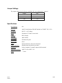
1
Synchrony
Cell Exchange
User's Guide
MC17358
October 1999
TimePlex Group Products
Americas
Europe/Middle East/Africa
Asia/Pacific
1619 North Harrison Parkway
Sunrise, Florida 33323-2802,
U.S.A.
Telephone: (800) 333-4143 or
(954) 846-1601
Fax: (954) 846-3935
Landata House, Station Road
Hook, Hampshire, RG27 9JF,
England
Telephone: 44 (0) 1256 763911
Fax: 44 (0) 1256 764717
c/o 1619 North Harrison Parkway
Sunrise, Florida 33323-2802,
U.S.A.
Telephone: (800) 333-4143 or
(954) 846-1601
Fax: (954) 846-3935
3/00
NO WARRANTIES ARE EXTENDED BY THIS DOCUMENT. The technical information in this document
is proprietary to Timeplex, Inc. and the recipient has a personal, non-exclusive and non-transferable
license to use this information solely with the use of Timeplex products. The only product warranties
made by Timeplex, Inc., if any, are set forth in the agreed terms and conditions for purchase of a
Timeplex product. Timeplex, Inc. disclaims liability for any and all damages that may result from
publication or use of this document and/or its contents except for infringement of third party copyright or
misappropriation of third party trade secrets. No part of this document may be reproduced in any manner
without the prior written consent of Timeplex, Inc.
U.S. GOVERNMENT RESTRICTED AND LIMITED RIGHTS
All software and related software documentation supplied to the United States Government are provided
with Restricted Rights. Use, duplication, or disclosure by the Government is subject to restrictions as set
forth in subparagraph (c)(1)(ii) of the Rights in Technical Data and Computer Software clause at DFARS
252.227-7013 or subparagraph (c)(2) of the Commercial Computer Software–Restricted Rights at CFR
52.227-19, as applicable.
All documentation, other than software documentation which are provided with Restricted Rights, are
provided with Limited Rights. U.S. Government rights to use, duplicate, or disclose documentation, other
than software documentation, are governed by the restrictions defined in paragraph (a)(15) of the Rights
in Technical Data and Computer Software clause at DFARS 252.227-7013 and FAR 52.227-19.
“DFARS” is the Department of Defense Supplement to the Federal Acquisition Regulation.
Manufacturer is Timeplex, Inc., 1619 North Harrison Parkway, Sunrise, Florida 33323-2802.
The information in this document is subject to change without notice. Revisions may be issued at such
time.
VT100 is a registered trademark of Digital Equipment Corporation.
Windows is a registered trademark of Microsoft Corporation.
Express Routing and LINK/100+ are trademarks of Timeplex, Inc.
ProComm is a registered trademark of Datastorm Technologies, Incorporated.
Intel is a registered trademark of Intel Corporation.
Timeplex, Synchrony, Express Switching, LINK/2+, and entréeLINK+ are registered trademarks of
Timeplex, Inc.
NOTICE
Telecommunications products must be installed and operated in compliance with the relevant National
Regulatory requirements summarized in the “REGULATORY” section of this manual. READ IN FULL,
PRIOR TO INSTALLATION, any product-specific National Regulatory requirements applicable to the
country of installation.
1998, 1999, 2000 Timeplex, Inc
ii
CXUG
3/15/00
User Manual Change Document
This change document revises information contained in the:
Synchrony Cell Exchange User's Guide (MC17358)
The information in this document supports Release 4.0.1 of the Synchrony Cell Exchange.
Insert this document directly after the title page of your manual as a record of the
change(s).
This change document addresses the following product features and other changes:
•
Dual Synchronous Legacy (DSL/DSL+) Module
•
Structured E1 Legacy (SEL) Module
•
Network Management (LANE and IP Configuration)
Front Matter
(1) Under “About This Manual,” the information should read:
This manual supports Release 4.0.1 of the Synchrony Cell Exchange system.
Chapter 1. Overview
(1) Page 1-11, in the first line of the paragraph titled, “Adaptive Timing,” change “DSL” to
“DSL/DSL+:”
MX17358-1
4/30/00
2000 Timeplex, Inc.
1 of 29
Chapter 2. Installation
(1) Page 2-5, replace the section titled, “Software Upgrade Requirements,” with the following:
Software Upgrade Requirements
Software upgrade requires:
•
IBM/compatible PC running Windows 95, Windows 98 or Windows NT
•
Terminal emulation software: HyperTerminal located in Windows 95, Windows 98 or
Windows NT Accessories
•
At least 5MB of hard disk space
CX Release 4.0.1 supports the FTP feature, which allows users to remotely update software
versions. The FTP feature allows CX users to save and restore databases and upload new software
from a remote location. The FTP feature requires use of an FTP Client application. Most simple
off-the-shelf FTP Client applications hosted on a PC or Unix workstation will work.
To upgrade a Cell Exchange device and configure a workstation to manage it:
•
Save the existing CX database, upgrade the software, and restore the CX database.
•
For detailed information on creating and restoring backups, see "Saving a Database Using
FTP" and "Restoring a Database Using FTP" in the "Operation" chapter of the Synchrony
Cell Exchange User's Guide.
•
For detailed information on upgrading Cell Exchange software, see the Synchrony Cell
Exchange 4.0.1 release notes.
However, not all off-the-shelf FTP Client applications can be used with the CX. The CX has
difficulty keeping up with FTP clients that send the FTP Server multiple segments at a time. These
sophisticated FTP Clients can be used only if configured to send one segment at a time.
The software upload feature requires use of both a telnet session and the FTP Client. Through the
Software Ver Menu screen the user selects the name of the new software version. The CX will
inform the user first, that it is erasing flash memory, and then, that it is ready to accept software.
Once the user sees the second prompt from the telnet screen the new software image can be sent to
the CX via the FTP Client. The following ftp command, FTP>put CPUROM.BIN, sends the
software image to the CX.
2 of 29
MX17358-1
4/30/00
Chapter 3. Modules
(1) Page 3-4, Table 3-1, add the following:
Structured E1 Legacy Interface
Module (SEL)
• Accepts synchronous non-cell (legacy) traffic and
converts the data to ATM CBR cells
• Places the cells on the ATM cell bus
• Monitors the physical interface
• Collects module performance statistics
(2) Page 3-51, delete the title and “Overview” paragraph and replace with the following:
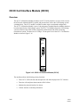
Dual Synchronous Legacy Interface Module
(DSL/DSL+)
Overview
The Dual Synchronous Legacy Interface Module (DSL/DSL+) is the gateway for synchronous non-ATM
traffic into the ATM network. The DSL/DSL+ module provides an EIA RS-530 interface, converts legacy
traffic into ATM cells, and establishes circuit emulation over the ATM network in AAL1 unstructured
mode. The DSL module supports data rates from 8 Kbps to 2.048 Mbps in 8 Kbps increments. The DSL+
module supports enhanced data rates of 1200 bps, 2400 bps, 4800 bps, 9600 bps, and 16 Kbps – 2.048
Mbps (in 8 Kbps increments). Adaptive Clock Recovery timing allows the module to be highly tolerant of
network timing ambiguities. The modules are differentiated by the addition of the “+” character on the
faceplate of the DSL+. A front panel view of the Dual Synchronous Legacy Interface Module is shown in
Figure 3-39 (DSL shown).
(3) Page 3-53, under Jumper Settings, insert the word “DSL” between “The” and “jumper” in the first
line. Add the following after the table and table note: “DSL+: There are no configurable jumper
settings.”
(4) Page 3-53, under Specifications/Data Rates, change the entry to read, “DSL: 8 Kbps – 2.048 Mbps
(in 8 Kbps increments), DSL+: 1200 bps, 2400 bps, 4800 bps, 9600 bps, and 16 Kbps – 2.048 Mbps
(in 8 Kbps increments).”
MX17358-1
4/30/00
3 of 29
(5) Page 3-53, insert the following note after Data Rates:
NOTE:
The lower port speeds will result in significantly increased
cellification delays. At 1200 bps, each cell is filled in ~313 ms.
Assuming a 3-cell delay end-to-end, there is a one-way delay of one
second, as measured from the input RS-530 port to the output of the
remote RS-530 port. If additional cell delay is introduced due to ATM
switching equipment, etc., then additional delays will be incurred.
The delays for the higher port rates are proportionately lower.
(6) Page 3-83, under Specifications/Port Speed, change to read, “8 Kbps – 4.096 Mbps (in 0.8 Kbps
increments).”
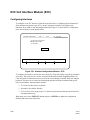
(7) After page 3-87, insert the following new information:
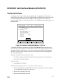
Structured E1 Legacy Module (SEL)
Overview
The Structured E1 Legacy Module (SEL) functions identically to the Structured T1 Legacy
Module except that it operates at 2.048 Mbps, and the framing format operates with 32 channels
rather than 24. The structured E1 Legacy Module terminates four (4) or eight (8) E1 interfaces,
accesses the DS0s within each E1, converts individual voice DS0s or individual/contiguous data
DS0s to individually addressable VPI/VCIs and converts them to AAL1-CBR formatted ATM
cells to be inserted into the ATM network.
The SEL Module allows voice and data contained in E1 channel groups (one or more 64KHz
channels) to be passed to and from ATM cell bearing equipment. The SEL Module supports either
four or eight E1 interfaces. Both Channel Associated Signaling (CAS) and CAS+CRC4 framing
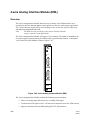
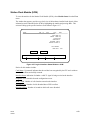
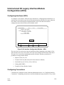
formats are supported (E1 interface configuration is discussed in the following section). Figure 368 shows the front panel of the SEL Module.
4 of 29
MX17358-1
4/30/00
SEL
SEL
OPNL
OPNL
A
C
A
C
E
G
B
D
B
D
F
H
A
A
E
B
B
F
C
C
G
D
D
H
SEL
4-Port
SEL
8-Port
Figure 3-68. Structured E1 Legacy Interface Module (SEL)
Channel groups are configured as either voice or data. For voice connections, the SEL enables
CAS (ABCD signaling bits for each channel) to be passed through the ATM network.
The user defines the various voice and data channel groupings via the SEL interface configuration
menu described in Chapter 5. Each channel group consists of one or more channels. The channels
can be either contiguous or non-contiguous.
SEL connections are established via the connection management menu (See "Configuring
Connections" in Chapter 5). The Cell Exchange allows any channel group to be connected to:
•
Any VPI/VCI of any configured cell bearing interface
•
Any “compatible” SEL channel group (any channel group that carries the same type of
traffic (voice or data) and contains the same number of channels)
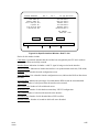
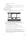
The SEL utilizes an AAL1 Segmentation And Reassembly (SAR) processor to pass data to and
from the ATM network. In Figure 3-69, two connections have been established between an E1
interface and the ATM network. In this example, E1 channels 2, 13, and 18 are mapped to one
VPI/VCI pair, and channels 3, 15, 27 are mapped to another VPI/VCI pair. Figures 3-70 and 3-71
show other possible connections.
MX17358-1
4/30/00
5 of 29
SEL
E1
SEL
E1
SEL
SAR
4 or 8 E1
Interfaces
1
.
.
.
.
.
.
E1
2
13
18
VPI/VCI
E1
channel
groups
ATM
Network
VPI/VCI
3
15
27
32
Two SEL-to-VPI/VCI connections
Figure 3-69. SEL Connection Using Two VPI/VCI Pairs
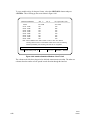
4 or 8 E1
Interfaces
SEL
SAR
1
.
.
.
.
.
.
E1
one
64K x 30
channel
group
2
3
.
.
.
.
32
VPI/VCI
ATM
Network
32
All 30 E1 (payload) timeslots mapped to one VPI/VCI pair
(non-payload timeslots 1 and 16 carry framing and signaling, respectively)
Figure 3-70. SEL Connection with Mapped Payload to One VPI/VCI Pair
4 or 8 E1
Interfaces
SEL
SAR
1
E1
.
.
.
.
.
.
32
30
64K
channel
groups
2
3
4
.
.
.
.
.
32
VPI/VCI
ATM
Network
VPI/VCI
Each E1 (payload) timeslot mapped to different VPI/VCI pairs
(non-payload timeslots 1 and 16 carry framing and signaling, respectively)
Figure 3-71. SEL Connection with Mapped Payloads to Different VPI/VCI Pairs
6 of 29
MX17358-1
4/30/00
For SEL-to-SEL connections, the actual channel numbers of each group may differ at each end as
long as each group contains the same number of channels. The ordering of channels passed from
the source channel group to the destination channel group is always preserved. In other words, the
first channel of the destination receives the data from the first channel of the source; the second
channel of the destination receives the data from the second channel of the source, and so on.
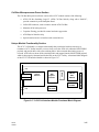
Cell Bus-Microprocessor-Power Section
The Cell Bus-Microprocessor-Power section of the SEL Interface Module consists of the
following:
•
ATM Cell Bus Switching Logic IC (ATM Cell Bus Switch), along with a RAM IC,
provides connectivity to the backplane board
•
96-Pin DIN connector, used to connect onto the ATM Cell Bus
•
Motorola 68340 microprocessor
•
Capacitor filtering, provided for control and noise suppression
Unique Functionality Section
The SEL Interface Module includes the following unique functions:
•
Module equipped with one complete independent synchronous channel
•
Connectors are RJ-45 female type
•
High-speed AAL1 segmentation and reassembly function
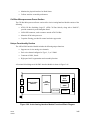
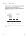
INTERFACE
DRIVERS & RECEIVERS
TYPE
FUNCTIONS
(AAL1)
ATM CELL
BUS
SWITCH
MEMORY
SRAM
CPU 68340
FILTERS
RJ45
DIN CONNECTOR
INTERFACE
DRIVERS & RECEIVERS
RJ45
RJ45
RJ45
LED
A functional block diagram of the SEL Interface Module is shown in Figure 3-72.
Figure 3-72. Structured E1 Legacy Interface Module Functional Block Diagram
MX17358-1
4/30/00
7 of 29
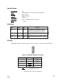
Specifications
Port Capacity:
Four or eight
Media:
Shielded Multi-twisted pair cable, low capacitance
Electrical:
EIA 530, DCE
Connector:
RJ-45
Line Format:
Balanced
Data Format:
ATM Cells
Line Build Out:
75 Norm, 120 Norm, 75 P.R., 120 P.R., 75 HRL1, 75 HRL2, and 120
HRL
Framing:
CAS+CRC4 or CAS
Port Speed:
2.048 Mbps
Granularity:
8 Kbps increments
Timing:
Synchronous Receive Timing, Adaptive Receive Timing, Internal or
External Transmit Timing Reference
Virtual Connections:
8 Port-Max. 240 AAL-1 type CBR, VPI/VCI connections
Timing:
Recovered, Internal, Reference, Onboard
Conditioning:
Trunk Conditioning Data Code (Idle (UAC) or MUX-OOS), Trunk
Conditioning Signaling (Idle (0)/Busy (1) or Busy (1)/Idle (0)), Idle
Channel Conditioning (Voice Idle or Data Idle)
Status & Statistics:
Standard status and statistics provided
Diagnostics:
Facility Loopback, Terminal Loopback
Alarm – Surveillance:
FIFO Overrun/Underrun
Translation Capacity:
256 VPIs, 10,240 VCIs
Power:
≤ 7 Watts
Standards Compliance: ITU G.703, G.804, af-vtoa-0078.000 Channel Emulation Service
8 of 29
MX17358-1
4/30/00
Indicators
Type
Label
Color
Meaning
LED
OPNL
Green
On Steady - Indicates that module is operational and has
successfully received configuration from CPU for at least
one E1 interface
On Blinking - Downloading program
Off - No power to module, no port configured, or CPU failed
LED
A thru D (4 port)
Green
Indicates that a configured port has achieved frame
synchronization with the received E1 when lit, loss of frame
synchronization when extinguished
or
A thru H (8 port)
Pinouts
Pinouts for the RJ-45 connector are shown in Figure 3-73 and the accompanying table.
12345678
1
2
4
5
Tx (to terminal equipment)
Rx (from terminal equipment)
Figure 3-73. SEL RJ-45 Pinouts
Pin
MX17358-1
4/30/00
Direction
Signal
Pin
Direction
Signal
1
To TE
Tx-R
4
To SEL
Rx-R
2
To TE
Tx-T
5
To SEL
Rx-T
9 of 29
Chapter 4. Operation
(1) Page 4-46, change “DSL” to “DSL/DSL+” wherever it appears.
(2) Page 4-46, add the following note at the bottom of the page:
NOTE:
On the module status screen, the same statistics will be displayed for
both modules. The only difference is that the DSL+ module will
display “DSL+” instead of “Sync Legacy.”
(3) Following page 4-57, insert the following new information:
Structured E1 Legacy Interface Module
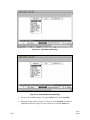
To view the statistics for the Structured E1 Legacy Interface Module (SEL), select Module Status
from the View menu.
The window that appears provides a top-level view of the hardware installed in the chassis.
Information is available for each slot, including module type and module status. More information
can be obtained for a particular module by highlighting the module and pressing <F2>. This action
will bring up the logical interface screen shown in Figure 4-60.
Intf Name
Intf Type
Slot:
Physical Intf
Middletown
SEL
7
A
Inact
Intf Status
Up
SCROLL UP LINE
SCROLL DOWN LINE
SCROLL UP PAGE
SCROLL DOWN PAGE
Press ENTER/F2 to go to the interface statistics screen
09:44
View: Intf: SEL
**ALARM**
**********
ESC-ESC = Previous
Figure 4-60. Logical Interface Status Window - SEL
The logical interface status window displays status information for each logical interface defined
for a specific module. In addition to configuration information (name, type, slot, physical interface,
active), the status of the interface is shown. This represents a snapshot of the current state of the
10 of 29
MX17358-1
4/30/00
interface – up or down. Additional information for each logical interface can be obtained by
highlighting the interface and pressing <F2>. The screen shown in Figure 4-61 will appear. This
screen contains information that is tailored to the interface.
Middletown
Name:
Framing:
Coding:
Traffic Type:
TC State:
TC Data Code:
TC Signaling:
Maj Alm Action:
CGA Status:
AIM Status:
BER Threshold:
Slot:
Type: Structured E1 Legacy
Intf: A
Card Status: Up
Port Status: Up
Loopback: No
ESF
0
SEL->ATM Cells:
HEC Error Cells:
Misrouted Cells:
Lost CLP Cells:
Lost Cell Seconds:
CLR
CLR
10-3
0
0
0
0
0
Last Statistics
Reset Hour: 13:00
REFRESH
16:25
7
CELL STATS
CLEAR
View: Intf: SEL
ESC-ESC = Previous
**********
Figure 4-61. Specific Interface Window—SEL
To view module activity for the past 8 hours, select the <CELL STATS> button and press
<ENTER>. This will bring up the screen shown in Figure 4-62.
Name:
Slot:
Middletown
Ch
Conn
Tx
Rx
Ch
0
3
6
9
12
15
18
21
24
27
30
N/A
N/A
N/A
N/A
N/A
N/A
1
4
7
10
13
16
19
22
25
28
31
REFRESH
16:28
View: Intf: SEL-CELL
7
Conn
Type: Structured E1 Legacy
Intf: A
Tx
Rx
Ch
Conn
Tx
Rx
2
5
8
11
14
17
20
23
26
29
CLEAR
**********
ESC-ESC = Previous
Figure 4-62. Interface Statistics Window—SEL
For each configured channel, a connection identifier and the number of cells transmitted and
received is displayed under the corresponding headings.
MX17358-1
4/30/00
11 of 29
Chapter 5. Configuration
(1) Page 5-28, change the Data Rate bullet to read, “Data Rate (edit field, “DSL: 8 Kbps – 2.048 Mbps
(in 8 Kbps increments), DSL+: 1200 bps, 2400 bps, 4800 bps, 9600 bps, and 16 Kbps – 2.048 Mbps
(in 8 Kbps increments)).”
(2) Page 5-28, insert the following note after the Data Rate bullet:
NOTE:
The lower port speeds will result in significantly increased
cellification delays. At 1200 bps, each cell is filled in ~313 ms.
Assuming a 3-cell delay end-to-end, there is a one-way delay of one
second, as measured from the input RS-530 port to the output of the
remote RS-530 port. If additional cell delay is introduced due to ATM
switching equipment, etc., then additional delays will be incurred.
The delays for the higher port rates are proportionately lower.
(3) Page 5-53, change the Data Rate bullet to read, “Data Rate (edit field, 8 Kbps – 4.096 Mbps in 0.8
Kbps increments)
(4) Following page 5-60, add the following new information:
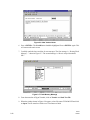
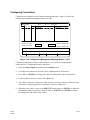
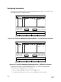
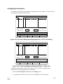
Structured E1 Legacy Interface Module Configuration
Configuring Interfaces
To configure a new Structured E1 Legacy Interface Module (SEL) interface, follow the steps
described in “Configuring Physical Interfaces” to enter the name, the interface type, the slot, the
physical interface and the active status indication. Press <F2> to enter the interface configuration
menu. Figure 5-56 shows the interface configuration menu with all fields set to the default values.
12 of 29
MX17358-1
4/30/00
Slot:
Intf Name: Middletown
Framing:
Line Build Out/Equal:
% Err Sec Threshold:
Tx Clock Out:
CAS+CRC4
75 Norm
100%
On Board
7
Intf: A
Intf Type: Structured E1
Trunk Conditioning Data Code:
Trunk Conditioning Signaling:
Idle Channel Conditioning:
ATM CES:
Idle (UAC)
Idle (0)/Busy (1)
Voice Idle
w/cas
Channel:
Conn:
0
N/ A
1
I
2
I
3
I
4
I
5
I
6
I
7
I
Channel:
Conn:
8
I
9
I
10
I
11
I
12
I
13
I
14
I
15
I
Channel:
Conn:
16
N/ A
17
I
18
I
19
I
20
I
21
I
22
I
23
I
Channel:
Conn:
24
I
25
I
26
I
27
I
28
I
29
I
30
I
31
I
Aggregate data rate for channel
grouping:
EXECUTE
Pre ss EN T E R T o up date the c onfig d ata ba se an d return to the M ain M en u
09:52
CFG: Intf: SEL
**********
ESC-ESC = Previous
Figure 5-56. Interface Configuration Window – SEL
The arrow keys are used to move between the different fields. Beginning at the "Framing" field, the
down arrow key can be used to move the cursor through each field in the following order (the space
bar is used to move through the possible selections, which are given below in parentheses starting
with the default):
•
Framing (CAS+CRC4, CAS)
•
Line Build Out/Equal (75 Norm, 120 Norm, 75 P.R., 120 P.R., 75 HRL1, 75 HRL2, 120
HRL)
•
% Err Sec Threshold (100%, 10%, 25%, 50%, 75%)
•
Tx Clock Out (On Board, Recovered, Ref Clock, Internal)
•
Trunk Conditioning Data Code (Idle {UAC}, MUX-OOS)
•
Trunk Conditioning Signaling (Idle {0}/Busy {1}, Busy {1}/Idle {0})
•
Idle Channel Conditioning (Voice Idle, Data Idle)
•
ATM CES (w/cas, basic)
When done, move to the EXECUTE button and press <ENTER> to update the configuration
database and return to the main menu.
MX17358-1
4/30/00
13 of 29
E1 Transmit Clock Configuration
For each configured SEL interface, one of four possible E1 transmit clock sources must be selected
in the interface configuration menu:
•
On Board (the default)
•
Recovered
•
Internal
•
Reference
On board means the E1 transmit clock is supplied by the SEL’s on board clock source.
Recovered means the E1 transmit clock is derived from the received E1 signal.
Internal means the E1 transmit clock is supplied by the main CPU board.
Reference means the E1 transmit clock is supplied by the currently configured reference clock
source (see Chapter 1, “System Timing”). Note that an SEL interface can be selected as the
reference clock source for the system.
It is important to note that SEL interfaces not configured to use recovered E1 transmit clock must
share the same E1 transmit clock configuration. For example, selecting Reference for one interface
automatically changes the clock configuration of all of the interfaces that are not configured for
recovered clock.
When done, move to the EXECUTE button and press <ENTER> to update the configuration
database and return to the main menu.
Configuring Channel Groups
The SEL interface configuration menu provides a channel assignment (data entry) field for each of
the 30 E1 “payload” channels. E1 timeslots 1 and 17 (channels 0 and 16) are reserved for framing
and signaling, respectively, and cannot be assigned to channel groups. These two channels are
marked N/A in the interface configuration menu. Whenever the cursor is positioned in one of the
channel assignment fields, the user is prompted as follows:
Channel assignment: Valid choices: I (idle), D1-D30
(data), V1-V30 (voice)
To configure a channel group, choose a unique channel group ID and enter it into each of the
channel assignment fields of the group. Channel group IDs for data channels begin with “D” and
channel group IDs for voice channels (signaling enabled) begin with “V.” Only one ID can be
assigned to a particular channel. An idle channel (a channel that does not belong to a group) is
configured by entering an “I” in the channel assignment field. All channels are initially idle when a
new interface is configured.
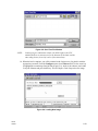
Configuring Connections
Connections are configured via the Connection Management menus. Figures 5-57 and 5-58 show
the configuration maps for SEL interfaces.
14 of 29
MX17358-1
4/30/00
Name: Middletown
Inact
Slot: 7
Intf:
A
Type: Structured E1
Chan
Dir
Interface Name
VPI VCI Chan
Connection Name Priority
V14/3
<-->
Germantown
2
German PBX200
12
SCROLL DOWN LINE
SCROLL UP LINE
EXECUTE
UPDATE
SCROLL UP PAGE
SCROLL DOWN PAGE
F1 - Execute
09:13
High
F3 - Add Connection
CFG: Con Mgmt:Map
**ALARM**
F4 - Delete Connection
******************
ESC-ESC = Previous
Figure 5-57. Connection Management Mapping Window – SEL to Cell Bearing
Name: Middleton
Inact
Slot: 7
Intf: A
Type: Structured E1
Chan
Dir
Interface Name
D5 /3
<-->
Columbia
D1/3
EXECUTE
UPDATE
VPI VCI Chan
Connection Name Priority
Columbia Three
SCROLL DOWN LINE
SCROLL UP LINE
SCROLL UP PAGE
F1 - Execute
10:51
High
CFG: Con Mgmt:Map
SCROLL DOWN PAGE
F3 - Add Connection
**ALARM**
F4 - Delete Connection
******************
ESC-ESC = Previous
Figure 5-58. Connection Management Mapping Window – SEL to SEL
Configuring connections to and from SEL interfaces is very similar to configuring other
connections (see “Configuring Interface Connections”).
1. Select the Connect Mgmt command from the Configure menu.
2. To configure the connections, move the cursor to highlight one of the interfaces.
3. Press <F2> or <ENTER> to bring up the connection management map for that interface.
MX17358-1
4/30/00
15 of 29
4. Use the Up/Down arrow key to move to the Inact field.
5. Press <F3> to add a new connection or <F4> to delete an existing connection. Follow
the steps described in “Configuring Interface Connections” to add new connections.
6. When done, press <F1> or move to the EXECUTE button and press <ENTER> to
update the configuration database and return to the main menu, or UPDATE and
<ENTER> to update the configuration and remain in this window.
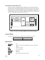
Network Management – Cell Exchange Networks
To manage Synchrony Cell Exchange devices, the devices must be configured for either LANE or
Classical IP management. For additional information, refer to "Configuring Cell Exchanges
Devices for LANE or Classical IP" below.
Configuring Cell Exchange Devices for LANE or Classical IP
The following sections provide introductory information on LANE and Classical IP and procedures
for configuring a CX network to use LANE or Classical IP.
LAN Emulation (LANE)
Many organizations are migrating networks to ATM to meet rising demands for bandwidth. The
challenge is how to support existing Ethernet and Token Ring LANs while migrating to ATM or
integrating ATM only for parts of the network. Users want applications to run transparently over
the network, whether it is an Ethernet, Token Ring, or ATM LAN.
LAN switches are an economical way to increase bandwidth without requiring expensive changes
to adapters, wiring, network software, or applications. LAN switches can deliver high-speed,
dedicated connections to individual users and combine bandwidth for better performance. LAN
switches also enable the creation of virtual LANs (VLANs), groupings of users based on logical
function rather than physical location.
In networks that incorporate both ATM and existing LAN technology, LAN-to-ATM conversion
functions become important. LAN Emulation (LANE) provides one option for this conversion.
LANE is a bridging protocol that makes a connection-oriented ATM network look and behave like
a shared, connectionless Ethernet or Token Ring LAN segment. LANE can handle both routable
protocols such as TCP/IP, IPX, and DECnet as well as non-routable protocols such as NetBIOS
and SNA.
LANE offers several advantages:
16 of 29
•
Users can take advantage of the higher speeds supported by ATM and access ATM
devices without replacing their investment in current LAN hardware, software, and
applications.
•
Ethernet, Token Ring, and ATM endstations continue to communicate as if they were on
the same LAN using standard procedures, because the ATM backbone is transparent to
the user.
MX17358-1
4/30/00
•
The LANE protocol defines how endstations communicate with each other across an ATM
network and how ATM-attached servers communicate with devices on Ethernet and Token
Ring LANs.
LANE works as a bridging protocol at layer 2 of the Open Systems Interconnection (OSI) model.
It does not emulate all of the actual media access control (MAC) protocols. The LANE protocol
focuses on emulating a single LAN segment by providing the connectionless broadcast service
required by network layer protocols, performing the necessary conversion of data between LAN
packets and ATM cells, and resolving MAC to ATM addressing.
LANE provides a translation layer between the higher-level connectionless protocols and the lowerlevel connection-oriented ATM protocols. The ATM adaptation layer (AAL) sits above the ATM
layer. The AAL formats data into the 48-byte ATM cell payload, a process known as
segmentation. Once the ATM cells reach their destination, they are reconstructed into higher-level
data and transmitted to the respective local devices, a process called reassembly. Because ATM
can carry multiple traffic types, several adaptation protocols, each operating simultaneously, can
exist at the adaptation layer. AAL Type 5 is used for LAN Emulation.
LANE sits above AAL5 in the protocol hierarchy. It masks the connection setup and handshaking
fluctuations required by the ATM network from the higher protocol layers and is independent of
upper-layer protocols, services, and applications. It maps the MAC address-based data networking
protocols into ATM virtual connections so that the higher-layer protocols think they are operating
on a connectionless LAN.
Two primary applications utilize the LANE protocol:
•
Centralizing servers and using ATM adapters to attach them directly to an ATM network.
•
Integrating existing LANs over an ATM transport backbone.
ATM switches that perform cell relay and use standard ATM signaling protocols to set up virtual
connections are not aware of the LANE protocol. LANE services can be co-located in an ATM
switch, but the switch fabric does not directly perform any of the emulation functions. The ATM
switch maintains the virtual connections and performs the cell-relay necessary for communication
over the ATM network.
LANE follows a client/server model, with multiple clients connecting to LAN Emulation
components. A LAN Emulation Client (LEC) provides data forwarding and address resolution
services. The LEC provides standard Ethernet or Token Ring LAN interfaces to any higher-layer
entity, such as the layer 3 IP and IPX protocols. Each ATM adapter, router, or LAN switch can
support multiple instances of an LEC, with a separate LEC for each connected Emulated LAN
(ELAN).
Clients are typically implemented on devices such as adapters or LAN switches, while LANE
clients and LAN Emulation Servers (LES) can be implemented together in a router, LAN or ATM
switch, or a standalone ATM equipped host. ATMARP (Address Resolution Protocol) Servers can
also be distributed on different routers, switches or hosts across the ATM network.
MX17358-1
4/30/00
17 of 29
LANE defines three different types of server components: the LAN Emulation Server (LES), the
Broadcast and Unknown Server (BUS), and the LAN Emulation Configuration Server (LECS).
These servers provide the following services:
•
Resolve MAC addresses to ATM addresses (LES)
•
Perform direct unicast data transfers and multi/broadcast data distribution among LAN
Emulation clients on the emulated LANs (ELANs) (BUS)
•
Maintain the relationship between emulated LANs and VLANs (LECS)
The LAN Emulation Server (LES) provides address resolution services (or "directory assistance")
that resolve Ethernet or Token Ring MAC addresses to ATM addresses. The LES itself is
identified by a unique ATM address. LECs can communicate directly with each other only when
they are connected to the same LES. Multiple LESs can exist on the same physical ATM LAN,
each LES supporting a different emulated LAN.
The Broadcast and Unknown Server (BUS) receives all broadcast and multicast packets and
transmits these messages to every member of the emulated LAN. A LEC is associated with only a
single BUS for each emulated LAN. Each BUS is identified by a unique ATM address, which the
LES associates with a broadcast MAC address.
The LAN Emulation Configuration Server (LECS) maintains configuration information about the
ATM network and supplies the address of the LES to a LEC when it is initialized. With this
information, LECs can perform their own configuration and join networks automatically. The
LECS also enables network administrators to control which physical LANs are combined to form
VLANs. The LECS assigns individual LANE clients to emulated LANs through the LES. One
LECS serves all emulated LANs within an administrative domain.
The LECS is responsible for dynamically assigning different LECs to different emulated LANs. It
provides the clients with the address of the most appropriate LES and maintains a database of the
resultant associations. It can assign a LEC to an emulated LAN based on either physical location,
as specified by the LEC's ATM address, or by logical association. A single LECS can manage the
configuration information for a very large ATM network, since its responsibilities are limited to
initial configuration. LECs communicate with the LAN Emulation service functions through two
different types of VCCs:
•
Control connections carry administrative messages, such as requests for initial
configuration and for addresses of other LECs.
•
Data connections handle all other communications. In particular, they link clients to each
other for data-direct unicast communications, and they link clients to the BUS for
broadcast and multicast messages.
While legacy LANs make heavy use of multipoint-to-multipoint broadcast, ATM supports only
point-to-point (unicast) and point-to-multipoint (broadcast or multicast) connections. The LES and
BUS work together to transfer unicast and broadcast traffic:
18 of 29
•
The LES handles address resolution and control information. Its primary job is to register
and resolve MAC addresses to ATM addresses.
•
The BUS is designed for carrying broadcast data, such as TCP/IP address resolution
broadcasts or Novell Service Advertising Protocol (SAP) messages. It also handles all
multicast traffic. Finally, it broadcasts the initial unicast frames sent by the LEC while the
MX17358-1
4/30/00
LES works in tandem to provide the appropriate ATM address for establishing a datadirect VCC.
Joining an ATM Network
When a LEC first powers up, it must obtain configuration information from the LECS in order to
join an emulated LAN. The LANE specification offers several options for locating the LECS:
•
The LEC can use a "well-known address" as defined by the ATM Forum. The Well
Known Address for finding the LECS is:
ICD - (Old) - 47.00.79.00.00.00.00.00.00.00.00.00.00.00.A0.3E.00.00.01.00
ICD - (New) - C5.00.79.00.00.00.00.00.00.00.00.00.00.00.A0.3E.00.00.01.00
•
The LECS can also be bypassed completely by configuring the ATM address of a LES in
the LEC.
Once the LEC locates the LECS, it sets up a connection and forwards some useful information,
such as its ATM address, its MAC address, its LAN type, and its maximum frame size. The LECS
responds with the actual LAN type, the actual maximum frame size, and the ATM address of a
LES. By providing a LES address, the LECS implicitly assigns the LEC to an emulated LAN.
Joining an Emulated LAN
Once a LEC knows the ATM address of the LES, it sets up a connection to the LES. When the
LES receives the connection setup message from the client, it learns the LEC's ATM address from
the calling party field in the message. Typically, it responds by adding the LEC as a leaf node on a
point-to-multipoint connection.
The LEC then registers its MAC address and associated ATM address with the LES, and the LES
assigns the client an LEC ID. The specification allows the LES to either discard the address or
store it for future reference. At this point, the LEC now can resolve MAC addresses to ATM
addresses.
Classical IP
Classical IP over ATM (CLIP) integrates IP and ATM technologies and minimizes the changes
required to accommodate the technology in existing routers, switches, and hosts. The end-to-end IP
routing architecture is the same as with legacy LAN technologies such as Ethernet. Classical IP
over ATM is a straightforward protocol that is easy to understand and implement for net managers
familiar with configuring IP nets. Classical IP can run over both ATM permanent virtual circuits
(PVCs) and switched virtual circuits (SVCs). It also supports logical IP subnets and allows net
managers to define ATM quality of service features on a subnet-by-subnet basis.
Perhaps the most significant virtue of Classical IP over ATM is its simplicity. In a simple PVC
network, IP addresses are mapped to virtual circuits, or virtual connections, manually. The user
configures each station with a local address table that specifies which virtual connection
corresponds to each IP address on the ATM network.
MX17358-1
4/30/00
19 of 29
Classical IP over ATM requires no changes to a conventional router-based internetwork. Classical
IP can be routed in the same way as conventional IP--packets are forwarded from the originator to
a router and from router to router until reaching the final destination. Along the way, the IP header
and upper-layer protocols and data remain essentially unchanged.
The prerequisite for two ATM stations to communicate with each other over an ATM network is
that each station knows the other station's ATM address. When a workstation starts up, it does not
know which other workstations are on the network, and, as it cannot broadcast to every station on
the network, another way of doing this is needed.
The ARP server performs the function of giving out the ATM address of stations on the ATM
network. It is a software-based process, and can reside on either a switch or a server/host. There
can only be one ARP Server per Logical IP Subnet (LIS), but one LIS can support more than one
LIS.
Hosts that are incapable of supporting Classical IP over ATM must have static entries made in the
ARP server's cache, with a mapping of IP address to an appropriate PVC. This will allow a CLIP
host to talk to a non-CLIP host. In order that communication may take place in the opposite
direction, static entries must be made in the opposite direction for every CLIP host that the nonCLIP host wishes to communicate with.
Because ATM is a connection oriented technology, the traditional Address Resolution Protocol
used on broadcast networks is no longer sufficient. To use SVCs, end-stations must have a way of
mapping IP addresses into ATM addresses and virtual connections automatically on demand. CLIP
solves this problem by specifying an ATMARP server, which performs address resolution for
network endpoints. The ATMARP server may be a software module running on a file server or
workstation, or it may be built into a router or ATM switch on the network.
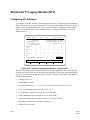
Configuring the CX Network
The following subsections provide information on:
•
Configuring the CX network to use either LANE or classical IP
•
Configuring the network for TELNET connections
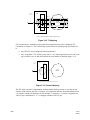
Connecting the Workstation Using LANE
SVC/LANE management support is provided by incorporating a LANE Client onto the Cell
Exchange (CX). This allows any standard SNMP manager to manage the CX. However, to take
advantage of the Cell Exchange GUI SNMP manager, it must be connected as shown in
Figure 5-59. The SNMP platform connects via the same ATM OC-3 NIC as used in previous
releases, but connects to the ATM network cloud versus directly to a CX node.
20 of 29
MX17358-1
4/30/00
Workstation
ATMARP Server
NIC
OC-3
AAL5
Pt-to-Pt
Connection
Workstation
Logical
Connections
(VPI/VCI)
NIC
OC-3
ATM Network
AAL5
Pt-to-Pt
Connection
CX-1500
CX-1500
CX-1540
Management Connection (SVP)
LANE Service Connection (Logical)
Figure 5-59. Logical Connectivity for LANE
Incorporating SVC and LANE allows management via IP addresses versus PVCs. An ATM
network with LANE must have an “ATMARP Server” in the network. The ATMARP Server
provides the function of tabling and/or converting IP and ATM addresses. ATM Gateways provide
the LES, LECS, and BUS services required for LANE operation. The ATMARP Server and ATM
Gateway can be the same ATM device. A “Lane Client” resides in both the Cell Exchange and the
ATM SNMP management platform in order to “communicate” via the ATMARP Server.
The network management workstation connection to the ATMARP Server is through an OC3
interface. This can be a CX-1500/CX-1540/CX-1580 OC3 module or an OC3 interface on a Fore
switch ATMARP Server.
Other devices can connect to the network using OC3 interfaces or non-OC3 interfaces for their
SNMP channels. For example, you could route an SNMP channel to a DS3 interface on a Fore
switch ATMARP Server.
To establish network management using LANE, you must:
1. Add an ATMARP Server to your ATM Network.
2. Configure the SNMP connection to the ATMARP Server (may be OC3 interface on CX
or on Fore switch).
3. Configure LANE connections for the network.
4. Connect the network management workstation to the OC3 interface.
5. Install and configure HP OpenView and Synchrony SNMS+ software on the network
management workstation.
MX17358-1
4/30/00
21 of 29
Adding an ATMARP Server to your ATM Network
TimePlex has qualified Fore Systems ForeRunner ATM switches for use as ATMARP Servers.
This includes the ASX-200 and the ASX-1200. For more information, contact your TimePlex sales
representative.
Configuring the SNMP Connection to the ATMARP Server
The network management workstation connection to the ATMARP Server is through an OC3
interface. This can be a CX-1500/CX-1540/CX-1580 OC3 module or an OC3 interface on a Fore
switch ATMARP Server. The sample procedure below pertains to an OC3 interface on a CX1500/CX-1540/CX-1580. For information on configuring SNMP connections for other equipment
types, see the user documentation for the ATMARP Server hardware you have chosen.
To configure the SNMP connection to the ATMARP Server:
1. From the CX-1500/CX-1540/CX-1580 craft display, select the SNMP command from
the Configuration menu.
2. Tab to Logical Intf and toggle the field until the OC3 module appears (use the space bar
for toggling).
3. Move to the Service Type field and toggle to IP.
4. Move to the Telnet Disconnect Timeout and enter a timer expiration in seconds (60 to
999).
5. Move to the IP button and press <ENTER>.
6. When the next window appears, tab to the VPI field and enter a VPI (e.g., 0).
7. Tab to the VCI field and enter a VCI (e.g., 33).
NOTE:
If the CPU is directly connected to the HRIM, the VPI/VCI values
cannot be modified.
8. Tab to Execute and press <ENTER>.
The OC3 is now configured to route SNMP data on VPI/VCI 0/33.
Configuring LANE Connections
To configure LANE connections, perform the following:
1. From the CX-1500/CX-1540/CX-1580 craft display, select the SNMP command from
the Configuration menu.
2. Tab to Logical Intf and toggle the field to select the SNMP interface (normally this is an
OC3).
3. Move to the Service Type field and toggle to LANE.
4. Move to the Telnet Disconnect Timeout and enter a timer expiration in seconds (60 to
999).
5. Move to the LANE button and press <ENTER>.
22 of 29
MX17358-1
4/30/00
6. When the LANE configuration window opens, enter the ATM Address (the CX MAC
address).
NOTE:
If the address appears as 00000000000000 (14 zeros), the user
should go back and assign a MAC address:
NOTE:
•
Go to the login screen (shift Q or remove/reinsert serial cable).
•
Enter the password: macman
•
Enter the 12 digit hex code for the MAC address (009010
followed by the CPU serial number). This only applies to the
ACTIVE CPU in a redundant CPU configuration.
The user does not have to modify this field if the MAC address is set.
It will be retained automatically.
7. Enter an IP address for this CX device.
8. Enter the subnet mask (e.g. 255.0.0.0).
NOTE:
In Step 9 below, any LANE component (LES, LECS, or BUS) you are
not required to enter must already be defined in the network.
9. Select the LECS ADDR Method (AUTO, PROG, ILMI, or NONE).
•
AUTO – user does not enter LECS, LES or ELAN (use well-known address).
•
PROG – user enters LECS only.
•
ILMI – not currently implemented
•
NONE – user enters LES address.
10. Enter the gateway IP address.
11. Enter the IP address(es) to which to send traps.
12. Enter the name of the Emulated LAN to join.
Connecting the Workstation to an OC3 Interface
Establishing a LANE connection to a network management workstation requires:
•
Fore ATM Network Interface Card (NIC) (200E/OC3SC).
•
An OC3 module on the CX-1500/CX-1540/CX-1580 device or an OC3 interface on the
ATMARP Server.
•
A multimode fiber-optic cable to connect the NIC card to the OC3 module
You must:
MX17358-1
4/30/00
•
Install the FORE ATM NIC card on the network management workstation
•
Install and configure the driver software on the network management workstation
•
Connect the NIC card to an OC3 interface using a multimode fiber-optic cable.
23 of 29
Included with the NIC card is a CD-ROM ForeRunner 200E ATM Network Adapters for UNIX
that includes ForeThought 4.1.
For information on installing the NIC card and installing and configuring the corresponding
software, see the ForeRunner SBA-200E ATM SBus Adapter User's Manual included on the CDROM.
Connecting the Workstation Using Classical IP
IP management support is provided by incorporating Classical IP into the Cell Exchange (CX).
This allows any standard SNMP manager to manage the CX. The SNMP platform connects via
10BaseT Ethernet to the HRIM module of the CX root node. To take advantage of the Cell
Exchange GUI SNMP manager, connections must be established as described below:
•
Static route between HRIM and the CPU at the root node
(Figure 5-60).
•
Remote node CPUs to the HRIM in the CX root node
(Figure 5-61).
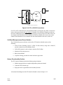
Workstation
2.0.0.2 HRIM
ATM IP
NOTE: Static routes (dashed lines) are
required to route IP HRIM to CPUs.
Ethernet
IP 1.0.0.1
HRIM
2.0.0.1 CPU ATM IP
CPU
(RIP =>)
Local LAN Segment
1.0.0.2 HRIM LAN IP
Figure 5-60. Classical IP Workstation Connectivity (Root Node)
The HRIM broadcasts RIP towards the local LAN segment and dynamically discovers the routes
for LAN devices on the local LAN segment. In order to pass IP across the network, static routes
must be configured into the HRIM for each remote LAN route. A static route must also be defined
between the HRIM and the CPU in order to pass SNMP from the workstation to the CPU module.
Static routes must be configured from HRIM to HRIM and from HRIM to CPU (within a CX
node).
The HRIM supports 32 static routes. Therefore, only 32 CX nodes can be managed using Classical
IP.
NOTE:
24 of 29
The IP address of the ATM side of the local HRIM must be on the
same IP subnet as all participating CPUs and remote HRIMs.
MX17358-1
4/30/00
In the configuration shown in Figure 5-61:
•
The SNMP platform connects via 10 base-t Ethernet to the HRIM module of the CX root
node. The ATM OC-3 NIC card is not required for this connection.
•
The originating PC/NMS system must have an IP address that is on the same IP subnet as
the HRIM.
•
The originating PC/NMS system must have a static route from the HRIM to the node(s)
being managed.
•
The HRIM supports a maximum of 32 static routes, including the HRIM to HRIM and
HRIM to CPU. This means only 32 CX nodes can be managed using Classical IP.
Workstation
2.0.0.2 HRIM
ATM IP
Ethernet
IP 1.0.0.1
HRIM
2.0.0.1 CPU ATM IP
CPU
(RIP =>)
Local LAN Segment
1.0.0.2 HRIM LAN IP
CX-1540
CPU IP 2.0.0.3
CX-1540
CPU IP 2.0.0.8
CX-1500
CPU IP 2.0.0.5
HRIM
NOTE: Static routes (dashed lines) are
required to route IP HRIM to CPUs. For
a different workstation, the SNMP must
be routed through the original (root)
HRIM.
(RIP =>)
CPU
CX-1500
CPU IP 2.0.0.4
Management Traffic
CPU
CPU
ATM IP 2.0.0.0
CX-1500
CPU IP 2.0.0.7
Local LAN Segment
Second or Other
Workstation
Figure 5-61. Classical IP Workstation Connectivity (Additional Nodes)
MX17358-1
4/30/00
25 of 29
Chapter 6. Troubleshooting
(1) Page 6-1, delete the bullets listed under “Traps” and replace with the following:
26 of 29
•
Power Supply UP
•
Standby CPU Active
•
Power Supply DOWN
•
CPU Manual Switchover
•
Board UP
•
CPU Manual Switchover Enabled
•
Board DOWN
•
CPU Manual Switchover Disabled
•
Incorrect Board Configured
•
CPU Switchover Requested
•
Interface UP
•
CPU Enable Switchover Requested
•
Interface DOWN
•
CPU Disable Switchover Requested
•
Management Validation Bad
•
AXS Failure
•
LEC UP
•
AXS Cleared
•
LEC DOWN
•
AXS Bad Location
•
Incorrect Password
•
AXS Bad Address
•
Software System FULL
•
AXS Bad Configuration
•
Software Version Removed
•
Incorrect OC3 timing
•
Download Good
•
Crypto parameters
•
Download Bad
•
Alarm Array members
•
Multicast Connection
•
CPU Not Ready
•
Validation Bad
•
CPU Ready
•
CPU ACTIVE
MX17358-1
4/30/00
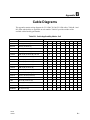
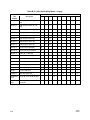
Appendix B. Cable Diagrams
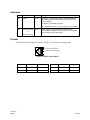
(1) Page B-2, replace Table B-2 with the following:
Table B-2. Cable Applicability Matrix – Legacy
Module Type
Part
Number
Description
STL
SEL DSL HSL HRIM LSAL UTEL HSSL UD3L UE3L
613008-X
HDB-26 (M) to DB-25 (M), RS530
X
X
613009-X
HDB-26 (M) to DB-25 (F), RS530
X
X
613004-X
HDB-26 (M) to DB-25 (M)
X
X
613005-X
HDB-26 (M) to DB-37 (M)
X
X
613006-X
HDB-26 (M) to DB-37 (F)
X
X
613003-X
HDB-26 (M) to DB-34 (M)
X
X
613007-X
HDB-26 (M) to DB-34 (F)
X
X
610127-X
RJ-45 to RJ-45 (Straight)
X
X
X
610126-X
RJ-45 to RJ-45 (Crossover)
X
X
X
612751-X
HSSI (M) to DCE (M)
X
612529-X
HSSI (M) crossover (M)
X
613013-X
RJ-45 (M) to 25-pin DTE (M)
X
613014-X
RJ-45 (M) to 25-pin DTE (F)
X
613015-X
RJ-45 (M) to 9-pin DTE (M)
X
613016-X
RJ-45 (M) to 9-pin DTE (F)
X
61359
DB-15 (M) to DB-15 (M)
X
61362
RJ-45 to DB-15 (F)
X
120405-X
BNC (M) to BNC (M)
X
COMATPX1013
RJ-45 (M) to RJ-45 (M) Straight
X
MX17358-1
4/30/00
X
X
X
27 of 29
(2) Pages B-3 and B-4, replace Table B-3 with the following:
Table B-3. Cable Index
Part No.
Cable Model
Connector
Figure
Description
650252-X
CPU-VT100/9F
9 Pin DB (F) –9 Pin DB (F)
B-1A
CPU craft interface to VT100 terminal
650074-X
CPU-VT100/25F
9 Pin DB (F) – 25 Pin DB (F)
B-1B
CPU craft interface to VT100 terminal
650075-X
CPU-VT100/25M
9 Pin DB (F) – 25 Pin DB (M)
B-1C
CPU craft interface to VT100 terminal
610133-X
ST/NCP-MDM
9 Pin DB (F) – 25 Pin DB (M)
B-2
CPU craft interface to VT100 terminal
via modem
613008-X
DSC-530M
26 Pin HDB (M) – 25 Pin DB
(M)
B-3
DSC Module (DTE) to RS-530 ATM
facility
DSL/ HSL Modules (DCE) and SCM
Module to V.11 (RS-530)
613009-X
DSC-530F
26 Pin HDB (M) – 25 Pin DB
(F)
B-3
DSC Module (DTE) to RS-530 ATM
facility
DSL/HSL Modules (DCE) and SCM
Module to V.11 (RS-530)
613004-X
DSL/HSL-ILC
26 Pin HDB (M) – 25 Pin DB
(M)
B-4
DSL/HSL Modules to LINK/2+ or
entréeLINK+ ILC Module
613005-X
DSL/HSL/SCM-449M
26 Pin HDB (M) – 37 Pin DB
(M)
B-5
DSL/HSL Modules to LINK/100+ DLI.0
Module and RS-449
SCM Module to RS-449
613006-X
DSL/HSL/SCM-449F
26 Pin HDB (M) – 37 Pin DB
(F)
B-5
DSL/HSL/SCM Modules to RS-449
613003-X
DSL/HSL/SCM-V35M
26 Pin HDB (M) – 34 Pin DB
(M)
B-6
DSC/DSL/HSL/SCM Modules to V.35
Winchester
613007-X
DSL/HSL/SCM-V35F
26 Pin HDB (M) – 34 Pin DB
(F)
B-6
DSC/DSL/HSL/SCM Modules to V.35
Winchester
61362
BADP
8 Pin Mod – 15 Pin DB (F)
B-9
STL Module to ST Dpanel-4/DSX-1 via
BIM/PBX cable (61359)
T1C Module to CSU/Smart Jack
(straight) via DSX-1/CSU cable (61385)
61359
BIM-PBX-F
15 Pin DB (M) – 15 Pin DB (M)
B-10
STL Module (via BADP cable) to ST
Dpanel-4/DSX-1
61385
DSX-1/CSU
15 Pin DB (M) – 15 Pin DB (M)
B-11
T1C Module (via BADP cable) to
CSU/Smart Jack
120405-X
TX3-DS3
Male/Male BNC
B-12
DS3 Module to DS3 (45Mbps) facility
(ANSI T1.107)
E3C Module to E3 equipment (34
Mbps)
E1C/UTEL Modules to G.703
unbalanced (via Balun)
HRIM Module to 10Base 2 Ethernet
UD3L/UE3L
28 of 29
MX17358-1
4/30/00
Table B-3. Cable Index (Cont’d)
Part No.
610126-X
Cable Model
ST/MOD-XFR
Connector
8 Pin Mod – 8 Pin Mod
Figure
B-8
Description
T1C Module to CSU/Smart Jack
(crossover)
E1C/SEL Module to E1 equipment
(crossover)
UTEL Module to non-framed E1 or T1
equipment (crossover)
610127-X
ST/MOD-MOD
8 Pin Mod – 8 Pin Mod
B-7
STL Module to LINK/2+ BFM/BIM.1,
LINK/100+ DLI.1 Module, entréeLINK+
CSU Module, or ST Dpanel-4/PRI
(T1M/E1M)
T1C Module to CSU/Smart Jack
(straight)
E1C/SEL Modules to E1 equipment
(straight)
UTEL Module to non-framed E1 or T1
equipment (straight)
612529-X
CXHSSI-XVR
HSSI (M) crossover (M)
B-22
HSSL Module crossover, HSSI 50-pin
connector
612751-X
CXHSSI-DCE
HSSI (M) to DCE (M)
B-21
HSSL Module to DCE, HSSI 50-pin
connector
613012-X
DSC – X.21
26 Pin HDB (M) – 15 Pin DB
(M)
B-15
DSC Module to V.11/X.21 (DCE)
613013-X
LSAL-RJ45-25DTE-M
RJ-45 (M) to 25-pin DTE (M)
B-17
LSAL Module to 25-pin DTE (for PCs or
workstations)
613014-X
LSAL-RJ45-25DTE-F
RJ-45 (M) to 25-pin DTE (F)
B-18
LSAL Module to 25-pin DTE (for most
non-PC DTEs)
613015-X
LSAL-RJ45-9DTE-M
RJ-45 (M) to 9-pin DTE (M)
B-19
LSAL Module to 9-pin DTE (for most
non-PC DTEs)
613016-X
LSAL-RJ45-9DTE-F
RJ-45 (M) to 9-pin DTE (F)
B-20
LSAL Module to 9-pin DTE (for PCs or
workstations)
COMATPX
1013
10 BASE T
RJ-45 (M) – RJ-45 (M)
B-16
HRIM Module to hub, 10Base-T
Ethernet (straight)
FOXN0004
OC3-SM
SC SM (M) – ST SM (M)
B-13
OC3 Module to 155 Mbps single mode
service (SONET)
FOXN0005
OC3-MM
SC MM (M) – SC MM (M)
B-14
OC3 Module to 155 Mbps multimode
service (SONET)
Appendix C. Cable Applications
(1) Page C-5, change the title of Figure C-9 to read, “E1C/SEL Module Cabling.”
MX17358-1
4/30/00
29 of 29
CXUG
10/6/99
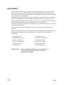
WARNING
NO OPERATOR SERVICEABLE PARTS ARE
INSIDE THIS EQUIPMENT. SERVICE MUST BE
PERFORMED BY QUALIFIED SERVICE
PERSONNEL.
VORSICHT
NICHT VOM BENUTZER REPARIERBARE TEILE IM
GEHÄUSE. BITTE WENDEN SIE SICH AN
QUALIFIZIERTES WARTUNGSPERSONAL.
ATTENTION
CET APPAREIL NE CONTIENT AUCUN ELÉMENT
QUE L'UTILISATEUR PUISSE RÉPARER. CONFIER
LA MAINTENANCE À UN PERSONNEL
TECHNIQUE QUALIFIÉ.
WARNING:
THIS EQUIPMENT MAY HAVE MORE THAN ONE
POWER SUPPLY CORD. DISCONNECT ALL
POWER SUPPLY CORDS BEFORE SERVICING TO
AVOID ELECTRICAL SHOCK.
VORSICHT:
DIESES GERÄT HAT MEHERE NETZANSCHLÜßE.
ZUR WARTUNG ALLE NETZKABEL TRENNEN UM
ELEKTRISCHEN SCHLAG ZU VERHINDERN.
ATTENTION:
CET APPAREIL COMPORT PLUS D'UN CORDON
D'ALIMENTATION AFIN DE PRÉVENIR LES CHOCS
ÉLECTRIQUES. DÉBRANCER TOUS LES
CORDONS D'ALIMENTATION AVANT LA
MAINTENANCE.
iii
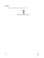
About This Manual
This manual supports Release 4.0 of the Synchrony Cell Exchange system.
The Synchrony Cell Exchange User’s Guide is part of the Synchrony library.
The primary purpose of the Synchrony Cell Exchange User’s Guide is to assist in installation,
initial configuration, and operation of a Cell Exchange system.
This manual is intended to supplement–not replace–formal training. Timeplex, Inc.
recommends that users obtain formal training prior to using this product. Contact the
Registrar at 1-954-846-6434 for information.
NOTES: Throughout this manual the term “system” and the expression “Cell
Exchange system” are used to apply to the CX family of Cell
Exchange Models, collectively.
The term “module” is used throughout this manual to represent
component cards that have specific application and have been
designed for use in the CX family of systems.
Organization of This Manual
This manual describes the Synchrony Cell Exchange system. This covers the physical design, basic
and expanded configurations, and the available modules to expand the system to meet the user’s
parameters.
The information is organized as follows:
iv
•
Chapter 1, Overview, provides a brief summary of ATM service, the family of Cell Exchange
models, common and interface modules, timing (or clocking), cooling and performance
characteristics.
•
Chapter 2, Installation, provides procedures for installing the Cell Exchange systems.
•
Chapter 3, Modules, describes each of the interface modules that can be used in the Cell
Exchange.
•
Chapter 4, Operation, describes basic procedures for operating the Cell Exchange system.
•
Chapter 5, Configuration, provides procedures for configuring individual Cell Exchange
modules.
•
Chapter 6, Troubleshooting, provides an overview of diagnostic procedures used to locate the
cause of malfunctions in Cell Exchange applications.
CXUG
3/15/00
•
Chapter 7, Replacement Procedures, provides step-by-step procedures for removing and
replacing field replaceable units.
Appendixes
•
Appendix A, Asynchronous Transfer Mode Overview, describes basic asynchronous
transfer mode (ATM) concepts.
•
Appendix B, Cable Diagrams, provides an index of Cell Exchange cables and cable wiring
diagrams.
•
Appendix C, Cable Applications, includes diagrams showing the types and applications of
cables used in a Cell Exchange system.
•
Appendix D, Field-Replaceable Units, provides an index of Cell Exchange field replaceable
items.
Index
Service
For service in the U.S. and Canada, contact Customer Support at 1-800-366-0126.
For service outside the U.S. and Canada, contact Customer Support at 44 (0) 1256 763911.
Information required for service is:
Model No. ________________________
Serial No. ______________________________
Warnings, Precautions, and Notes
Be sure that you understand all directions, warnings, and limitations before using this product. In
this manual:
CXUG
3/15/00
•
WARNINGS present information or describe conditions, which if not observed could result in
injury.
•
PRECAUTIONS reflect conditions that could cause product damage or data loss.
•
NOTES describe limitations on the use of the equipment or procedure.
v
If Product Is Received Damaged
Forward an immediate request to the delivering carrier to perform an inspection and prepare a
damage report. SAVE container and packing material until contents are verified.
Concurrently, report the nature and extent of damage to Customer Support so that action can be
initiated to repair or replace damaged items or instructions issued for returning items.
The responsibility of the manufacturer ends with delivery to the first carrier. ALL CLAIMS for
loss, damage, or nondelivery must be made against the delivering carrier WITHIN 10 DAYS OF
RECEIPT of shipment.
To Return Product
Please obtain instructions from Customer Support before returning any item(s). Report the fault or
deficiency along with the model, type, and serial number of the item(s) to Customer Support. Upon
receipt of this information, Customer Support will provide service instructions or a Return
Authorization Number and other shipping information. All items returned under this warranty must
be sent to the manufacturer with charges prepaid.
vi
CXUG
10/6/99
Contents
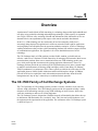
Overview ......................................................................................................1-1
THE CX-1500 FAMILY OF CELL EXCHANGE SYSTEMS .............................................. 1-1
Modules and Services.................................................................................................... 1-2
EQUIPMENT DESCRIPTION ............................................................................................. 1-4
CX-1500 ....................................................................................................................... 1-4
CX-1540 ....................................................................................................................... 1-5
CX-1580 ....................................................................................................................... 1-6
Power Distribution ........................................................................................................ 1-7
Indicators ...................................................................................................................... 1-7
CPU Module ................................................................................................................. 1-7
Power Supply Module ................................................................................................... 1-9
Station Clock Module.................................................................................................... 1-9
Interface Modules.......................................................................................................... 1-9
TIMING ..............................................................................................................................1-10
System Timing .............................................................................................................1-10
Data Bus Timing ..........................................................................................................1-10
Channel/Port Timing ....................................................................................................1-10
External Timing ...........................................................................................................1-12
SYSTEM COOLING...........................................................................................................1-16
PERFORMANCE CHARACTERISTICS ............................................................................1-17
COMPATIBILITY REQUIREMENTS................................................................................1-19
LINK Family................................................................................................................1-19
Synchrony ST ..............................................................................................................1-19
IAN-150.......................................................................................................................1-19
AD-10 ..........................................................................................................................1-19
Other Vendors’ Equipment ...........................................................................................1-19
Installation ...................................................................................................2-1
SITE PREPARATION.......................................................................................................... 2-1
EQUIPMENT INSTALLATION .......................................................................................... 2-1
Unpacking..................................................................................................................... 2-1
Required Tools and Equipment...................................................................................... 2-1
Chassis Installation Procedures...................................................................................... 2-1
Grounding Requirements............................................................................................... 2-2
Power Connections........................................................................................................ 2-2
Module Installation Procedures...................................................................................... 2-3
SOFTWARE INSTALLATION............................................................................................ 2-5
Diskette Installation....................................................................................................... 2-5
SOFTWARE UPGRADE REQUIREMENTS ....................................................................... 2-5
General Information ...................................................................................................... 2-5
Procedures for Software Upgrade .................................................................................. 2-6
Single CPU Scenario ..................................................................................................... 2-7
Flow Diagrams .............................................................................................................. 2-9
Loading New Software Using the Craft Interface..........................................................2-10
Loading New Software Using FTP ...............................................................................2-14
CXUG
10/6/99
vii
Loading New Software Using Xmodem........................................................................2-15
Software Download Process Considerations .................................................................2-20
SOFTWARE VERSIONS....................................................................................................2-22
Modules .......................................................................................................3-1
SUMMARY OF MODULES ................................................................................................ 3-1
CPU MODULE .................................................................................................................... 3-5
Overview....................................................................................................................... 3-5
Specifications ................................................................................................................ 3-7
Indicators ...................................................................................................................... 3-7
Pinouts .......................................................................................................................... 3-7
AC POWER SUPPLY MODULE ......................................................................................... 3-9
CX-1500 Chassis........................................................................................................... 3-9
Specifications ...............................................................................................................3-10
Indicators .....................................................................................................................3-11
CX-1540 Chassis..........................................................................................................3-11
Specifications ...............................................................................................................3-11
Indicators .....................................................................................................................3-11
DC POWER SUPPLY MODULE ........................................................................................3-12
Specifications ...............................................................................................................3-13
Indicators .....................................................................................................................3-13
STATION CLOCK MODULE (SCM).................................................................................3-14
Overview......................................................................................................................3-14
Specifications ...............................................................................................................3-15
Indicators .....................................................................................................................3-15
Pinouts .........................................................................................................................3-15
DUAL T1 CELL INTERFACE MODULE (T1C) ................................................................3-16
Overview......................................................................................................................3-16
Jumper Settings ............................................................................................................3-17
Specifications ...............................................................................................................3-17
Indicators .....................................................................................................................3-18
Pinouts .........................................................................................................................3-18
OC3 CELL INTERFACE MODULE (OC3) ........................................................................3-19
Overview......................................................................................................................3-19
Specifications ...............................................................................................................3-21
Indicators .....................................................................................................................3-23
Pinouts .........................................................................................................................3-23
OC3C CELL INTERFACE MODULE (OC3C) ...................................................................3-24
Overview......................................................................................................................3-24
Specifications ...............................................................................................................3-26
Indicators .....................................................................................................................3-28
Pinouts .........................................................................................................................3-28
DUAL SYNCHRONOUS CELL INTERFACE MODULE (DSC) .......................................3-29
Overview......................................................................................................................3-29
Jumper Settings ............................................................................................................3-31
Specifications ...............................................................................................................3-31
Indicators .....................................................................................................................3-32
Pinouts .........................................................................................................................3-32
DS3 CELL INTERFACE MODULE (DS3) .........................................................................3-33
Overview......................................................................................................................3-33
viii
CXUG
10/6/99
Specifications ...............................................................................................................3-35
Indicators .....................................................................................................................3-35
Pinouts .........................................................................................................................3-35
E1 CELL INTERFACE MODULE (E1C)............................................................................3-36
Overview......................................................................................................................3-36
Jumper Settings ............................................................................................................3-38
Specifications ...............................................................................................................3-38
Indicators .....................................................................................................................3-38
Pinouts .........................................................................................................................3-39
E3 CELL INTERFACE MODULE (E3C)............................................................................3-40
Overview......................................................................................................................3-40
Specifications ...............................................................................................................3-41
Indicators .....................................................................................................................3-42
Pinouts .........................................................................................................................3-42
STRUCTURED T1 LEGACY MODULE (STL)..................................................................3-43
Overview......................................................................................................................3-43
STL Operation..............................................................................................................3-46
Specifications ...............................................................................................................3-49
Indicators .....................................................................................................................3-49
Pinouts .........................................................................................................................3-50
DUAL SYNCHRONOUS LEGACY INTERFACE MODULE (DSL) .................................3-51
Overview......................................................................................................................3-51
Jumper Settings ............................................................................................................3-53
Specifications ...............................................................................................................3-53
Indicators .....................................................................................................................3-53
Pinouts .........................................................................................................................3-53
HIGH-SPEED SYNCHRONOUS LEGACY INTERFACE MODULE (HSL)......................3-55
Overview......................................................................................................................3-55
Jumper Settings ............................................................................................................3-57
Specifications ...............................................................................................................3-57
Indicators .....................................................................................................................3-57
Pinouts .........................................................................................................................3-58
HIGH-SPEED SERIAL INTERFACE LEGACY MODULE (HSSL)...................................3-59
Overview......................................................................................................................3-59
Jumper Settings ............................................................................................................3-61
Specifications ...............................................................................................................3-61
Indicators .....................................................................................................................3-61
Pinouts .........................................................................................................................3-61
HUB ROUTER LEGACY INTERFACE MODULE (HRIM)...............................................3-63
Overview......................................................................................................................3-63
Specifications ...............................................................................................................3-63
Indicators .....................................................................................................................3-64
Pinouts .........................................................................................................................3-64
LOW SPEED ASYNCHRONOUS LEGACY INTERFACE MODULE (LSAL).................3-65
Overview......................................................................................................................3-65
Specifications ...............................................................................................................3-66
Indicators .....................................................................................................................3-66
Pinouts .........................................................................................................................3-67
UNSTRUCTURED T1/E1 LEGACY INTERFACE MODULE (UTEL) ..............................3-68
Overview......................................................................................................................3-68
Jumper Settings ............................................................................................................3-70
CXUG
10/6/99
ix
Specifications ...............................................................................................................3-71
Indicators .....................................................................................................................3-71
Pinouts .........................................................................................................................3-72
UNSTRUCTURED DS3/T3 LEGACY INTERFACE MODULE (UD3L)............................3-73
Overview......................................................................................................................3-73
Jumper Settings ............................................................................................................3-75
Specifications ...............................................................................................................3-75
Indicators .....................................................................................................................3-76
Pinouts .........................................................................................................................3-76
UNSTRUCTURED E3 LEGACY INTERFACE MODULE (UE3L)....................................3-77
Overview......................................................................................................................3-77
Jumper Settings ............................................................................................................3-79
Specifications ...............................................................................................................3-79
Indicators .....................................................................................................................3-79
Pinouts .........................................................................................................................3-80
BASIC INTERFACE MODULE (BIM)...............................................................................3-81
Overview......................................................................................................................3-81
Jumper Settings ............................................................................................................3-83
Specifications ...............................................................................................................3-83
Indicators .....................................................................................................................3-83
4-WIRE ANALOG INTEFACE MODULE (EML)..............................................................3-84
Overview......................................................................................................................3-84
Jumper Settings ............................................................................................................3-86
Specifications ...............................................................................................................3-86
Indicators .....................................................................................................................3-86
Pinouts .........................................................................................................................3-87
Operation .....................................................................................................4-1
INITIAL STARTUP ............................................................................................................. 4-1
Local Management Station ............................................................................................ 4-1
Initial Logon.................................................................................................................. 4-3
MENU OPERATION ........................................................................................................... 4-5
Menu Selection.............................................................................................................. 4-6
Command Operation ..................................................................................................... 4-6
MAIN MENU....................................................................................................................... 4-7
Configure Menu ............................................................................................................ 4-8
View Menu ................................................................................................................... 4-9
Diagnostics Menu.........................................................................................................4-13
NETWORK MANAGEMENT ............................................................................................4-16
LANE Operation ..........................................................................................................4-17
IP Operation .................................................................................................................4-19
Setting the MAC Address of the CPU...........................................................................4-20
TELNET SUPPORT............................................................................................................4-20
Local Session ...............................................................................................................4-21
Remote Session ............................................................................................................4-25
FTP SUPPORT....................................................................................................................4-28
Saving a Database Using FTP.......................................................................................4-28
Restoring a Database Using FTP ..................................................................................4-29
ALARMS ............................................................................................................................4-29
MODULE STATISTICS .....................................................................................................4-30
x
CXUG
10/6/99
CPU Module (CPU) .....................................................................................................4-32
Station Clock Module (SCM) .......................................................................................4-33
Dual T1 Cell Interface Module (T1C) ...........................................................................4-34
OC3 Cell Interface Module (OC3) ................................................................................4-37
OC3c Cell Interface Module (OC3C)............................................................................4-39
Dual Synchronous Cell Interface Module (DSC)...........................................................4-40
DS3 Cell Interface Module (DS3).................................................................................4-41
E1 Cell Interface Module (E1C) ...................................................................................4-42
E3 Cell Interface Module (E3C) ...................................................................................4-43
Structured T1 Legacy Module (STL) ............................................................................4-44
Dual Synchronous Legacy Interface Module (DSL) ......................................................4-46
High-Speed Synchronous Legacy Interface Module (HSL) ...........................................4-47
High-Speed Serial Interface Legacy Module (HSSL) ....................................................4-48
Hub Router Interface Module (HRIM)..........................................................................4-49
Low Speed Asynchronous Legacy Interface Module (LSAL)........................................4-50
Unstructured T1 Legacy Interface Module (UTL) .........................................................4-52
Unstructured E1 Legacy Interface Module (UEL) .........................................................4-53
Unstructured DS3/T3 Legacy Interface Module (UD3L)...............................................4-54
Unstructured E3 Legacy Interface Module (UE3L) .......................................................4-55
Basic Interface Module (BIM) ......................................................................................4-56
4-wire Analog Interface Module (EML)........................................................................4-57
Configuration ..............................................................................................5-1
SETTING LOCATION NAME ............................................................................................ 5-1
CONFIGURING PHYSICAL INTERFACES ....................................................................... 5-2
SETTING SYSTEM TIMING .............................................................................................. 5-6
Network Clocking ......................................................................................................... 5-7
CONFIGURING INTERFACE CONNECTIONS................................................................. 5-7
STATION CLOCK MODULE (SCM).................................................................................5-10
Configuring Interfaces ..................................................................................................5-10
DUAL T1 CELL INTERFACE MODULE (T1C) ................................................................5-11
Configuring Interfaces ..................................................................................................5-11
Configuring Connections..............................................................................................5-12
OC3/OC3C CELL INTERFACE MODULE (OC3/OC3C)...................................................5-13
Configuring Interfaces ..................................................................................................5-13
Configuring Connections..............................................................................................5-14
DUAL SYNCHRONOUS CELL INTERFACE MODULE (DSC) .......................................5-15
Configuring Interfaces ..................................................................................................5-15
Configuring Connections..............................................................................................5-16
DS3 CELL INTERFACE MODULE (DS3) .........................................................................5-18
Configuring Interfaces ..................................................................................................5-18
Configuring Connections..............................................................................................5-19
E1 CELL INTERFACE MODULE (E1C)............................................................................5-20
Configuring Interfaces ..................................................................................................5-20
Configuring Connections..............................................................................................5-21
E3C CELL INTERFACE MODULE (E3C) .........................................................................5-22
Configuring Interfaces ..................................................................................................5-22
Configuring Connections..............................................................................................5-23
STRUCTURED T1 LEGACY MODULE (STL)..................................................................5-24
Configuring STL Interfaces ..........................................................................................5-24
CXUG
10/6/99
xi
Configuring STL Connections ......................................................................................5-25
DUAL SYNCHRONOUS LEGACY INTERFACE MODULE (DSL) .................................5-28
Configuring Interfaces ..................................................................................................5-28
Configuring Connections..............................................................................................5-29
HIGH-SPEED SYNCHRONOUS LEGACY INTERFACE MODULE (HSL)......................5-30
Configuring Interfaces ..................................................................................................5-30
Configuring Connections..............................................................................................5-31
HIGH-SPEED SERIAL INTERFACE LEGACY MODULE CONFIGURATION (HSSL) ..5-32
Configuring Interfaces ..................................................................................................5-32
Configuring Connections..............................................................................................5-33
HUB ROUTER INTERFACE MODULE (HRIM) ...............................................................5-34
Configuring Interfaces ..................................................................................................5-34
Channel Configuration..................................................................................................5-36
Configuring Connections..............................................................................................5-38
Verifying Network Operation .......................................................................................5-39
LOW SPEED ASYNCHRONOUS LEGACY INTERFACE MODULE (LSAL)..................5-41
Configuring Interfaces ..................................................................................................5-41
Configuring Connections..............................................................................................5-42
UNSTRUCTURED T1 LEGACY INTERFACE MODULE (UTL)......................................5-43
Configuring Interfaces ..................................................................................................5-43
Configuring Connections..............................................................................................5-44
UNSTRUCTURED E1 LEGACY INTERFACE MODULE (UEL)......................................5-46
Configuring Interfaces ..................................................................................................5-46
Configuring Connections..............................................................................................5-47
UNSTRUCTURED DS3/T3 LEGACY INTERFACE MODULE CONFIGURATION
(UD3L)...........................................................................................................................5-49
Configuring Interfaces (UD3L).....................................................................................5-49
Configuring Connections..............................................................................................5-50
UNSTRUCTURED E3 LEGACY INTERFACE MODULE CONFIGURATION (UE3L)....5-51
Configuring Interfaces (UE3L) .....................................................................................5-51
Configuring Connections..............................................................................................5-51
BASIC INTERFACE MODULE CONFIGURATION (BIM)...............................................5-53
Configuring Interfaces (BIM) .......................................................................................5-53
Configuring Connections..............................................................................................5-54
4-WIRE ANALOG INTERFACE MODULE CONFIGURATION (4-WIRE EML) .............5-55
Configuring Interfaces (4-Wire EML)...........................................................................5-55
Configuring Connections..............................................................................................5-56
MULTICAST FEATURE CONFIGURATION....................................................................5-57
Configuring Interfaces ..................................................................................................5-57
Limitations on Cell Exchange Multicast Operation Involving Legacy Interfaces ...........5-59
Troubleshooting..........................................................................................6-1
ALARMS AND TRAPS ....................................................................................................... 6-1
Traps............................................................................................................................. 6-1
Alarms - Craft Interface................................................................................................. 6-1
GENERAL TROUBLESHOOTING PROCEDURES ........................................................... 6-5
MODULE INDICATIONS ................................................................................................... 6-6
AC Power Supply Module ............................................................................................. 6-6
DC Power Supply Module ............................................................................................. 6-7
CPU Module ................................................................................................................. 6-7
xii
CXUG
10/6/99
Other Modules............................................................................................................... 6-7
USER-INITIATED TESTS................................................................................................... 6-7
Replacement Procedures...........................................................................7-1
ELECTROSTATIC DISCHARGE (ESD) ANTI-STATIC PROCEDURE............................. 7-1
REMOVING AND REPLACING CHASSIS ........................................................................ 7-1
REMOVING AND REPLACING MODULES ..................................................................... 7-2
Model CX-1500 Power Supply Module (AC or DC)...................................................... 7-2
CPU Module ................................................................................................................. 7-3
Other Modules............................................................................................................... 7-4
Appendixes
Asynchronous Transfer Mode Overview................................................. A-1
Cable Diagrams.......................................................................................... B-1
Cable Applications .................................................................................... C-1
Field-Replaceable Units ............................................................................ D-1
Index
Regulatory
CXUG
10/6/99
xiii
Figures
Figure 1-1. Cell Exchange System Architecture.................................................................................... 1-2
Figure 1-2. Cell Exchange System Interfaces........................................................................................ 1-3
Figure 1-3. CX-1500 Cell Exchange System......................................................................................... 1-5
Figure 1-4. CX-1540 Cell Exchange System......................................................................................... 1-6
Figure 1-5. CX-1580 Cell Exchange System......................................................................................... 1-6
Figure 1-6. System Timing Diagram (Page 1 of 3)...............................................................................1-13
Figure 1-6. System Timing Diagram (Page 2 of 3)...............................................................................1-14
Figure 1-6. System Timing Diagram (Page 3 of 3)...............................................................................1-15
Figure 1-7. Cell Exchange with Stacking Fan Unit ..............................................................................1-16
Figure 2-1. CX-1500 AC Power Connector Module (Rear Chassis)...................................................... 2-3
Figure 2-2. CX-1500 DC Power Connector Module (Rear Chassis)...................................................... 2-3
Figure 2-3. CX-1540 AC Power Connector Module (Rear Chassis)...................................................... 2-3
Figure 2-4. Configure Menu................................................................................................................2-10
Figure 2-5. Software Version Window ................................................................................................2-11
Figure 2-6. New Version Name...........................................................................................................2-12
Figure 2-7. Flash Memory Message.....................................................................................................2-12
Figure 2-8. Send Text File Window.....................................................................................................2-13
Figure 2-9. Loading New Image..........................................................................................................2-13
Figure 2-10. Configure Menu ..............................................................................................................2-16
Figure 2-11. Software Version Window ..............................................................................................2-16
Figure 2-12. New Version Name.........................................................................................................2-17
Figure 2-13. Flash Memory Message...................................................................................................2-18
Figure 2-14. Start Xmodem Send Message..........................................................................................2-18
Figure 2-15. Xmodem Selection Window............................................................................................2-19
Figure 2-16. Software Load Indicator Window....................................................................................2-19
Figure 2-17. Loading New Image........................................................................................................2-20
Figure 2-18. Software Version Command............................................................................................2-22
Figure 2-19. Software Version Selection Screen..................................................................................2-23
Figure 3-1. Front Panel of CPU Module (CPU) .................................................................................... 3-5
Figure 3-2. CPU Module Functional Block Diagram ............................................................................ 3-6
Figure 3-3. DB-9M Connector ............................................................................................................. 3-7
Figure 3-4. AC Power Supply Module (CX-1500)................................................................................ 3-9
Figure 3-5. AC Power Supply Module Functional Block Diagram.......................................................3-10
Figure 3-6. DC Power Supply Module (CX-1500D) ............................................................................3-12
Figure 3-7. DC Power Supply Module Functional Block Diagram.......................................................3-13
Figure 3-8. Station Clock Module (SCM)............................................................................................3-14
Figure 3-9. HDB-26F (DCE) Pin Location ..........................................................................................3-15
Figure 3-10. Dual T1 Cell Interface Module (T1C)..............................................................................3-16
Figure 3-11. Dual T1 Cell Interface Module Functional Block Diagram ..............................................3-17
Figure 3-12. Pin Location....................................................................................................................3-18
Figure 3-13. OC3 Cell Interface Module (OC3)...................................................................................3-19
Figure 3-14. OC3 Cell Interface Module Functional Block Diagram....................................................3-20
Figure 3-15. SC Duplex Connector .....................................................................................................3-23
Figure 3-16. OC3C Cell Interface Module (OC3C)..............................................................................3-24
Figure 3-17. OC3C Cell Interface Module Functional Block Diagram .................................................3-25
Figure 3-18. SC Duplex Connector .....................................................................................................3-28
Figure 3-19. Dual Synchronous Cell Interface Module (DSC) .............................................................3-29
xiv
CXUG
10/6/99
Figure 3-20. Dual Synchronous Cell Interface Module Functional Block Diagram...............................3-30
Figure 3-21. HDB-26F (DTE) Pin Location.........................................................................................3-32
Figure 3-22. DS3 Cell Interface Module (DS3)....................................................................................3-33
Figure 3-23. DS3 Cell Interface Module Functional Block Diagram ....................................................3-34
Figure 3-24. BNC Pin Location...........................................................................................................3-35
Figure 3-25. E1 Cell Interface Module (E1C) ......................................................................................3-36
Figure 3-26. E1 Cell Interface Module Functional Block Diagram.......................................................3-37
Figure 3-27. RJ-45 Pin Location..........................................................................................................3-39
Figure 3-28. E3 Cell Interface Module (E3C) ......................................................................................3-40
Figure 3-29. E3 Cell Interface Module Functional Block Diagram.......................................................3-41
Figure 3-30. BNC Pin Location...........................................................................................................3-42
Figure 3-31. Structured T1 Legacy Interface Module (STL) ................................................................3-43
Figure 3-32. T1 Mapping ....................................................................................................................3-44
Figure 3-33. Channel Mapping............................................................................................................3-44
Figure 3-34. STL to VPI/VCI Connections..........................................................................................3-45
Figure 3-35. Structured T1 Legacy Interface Module Functional Block Diagram.................................3-46
Figure 3-36. Trunk Conditioning.........................................................................................................3-47
Figure 3-37. Another Example of Trunk Conditioning.........................................................................3-48
Figure 3-38. STL RJ-45 Pinouts ..........................................................................................................3-50
Figure 3-39. Dual Synchronous Legacy Interface Module (DSL).........................................................3-51
Figure 3-40. Dual Synchronous Legacy Interface Module (DSL) Functional Block Diagram...............3-52
Figure 3-41. HDB-26F (DCE) Pin Location ........................................................................................3-54
Figure 3-42. High Speed Synchronous Legacy Interface Module (HSL) ..............................................3-55
Figure 3-43. High Speed Synchronous Legacy Interface Module Functional Block Diagram ...............3-56
Figure 3-44. HDB-26F (DCE) Pin Location ........................................................................................3-58
Figure 3-45. High Speed Serial Interface Legacy Module (HSSL) .......................................................3-59
Figure 3-46. High Speed Synchronous Legacy Interface Module Functional Block Diagram ...............3-60
Figure 3-47. HSSL Pin Location .........................................................................................................3-62
Figure 3-48. Hub Router Legacy Interface Module (HRIM) ................................................................3-63
Figure 3-49. BNC Pin Location...........................................................................................................3-64
Figure 3-50. RJ-45 Pinouts..................................................................................................................3-64
Figure 3-51. Low Speed Asynchronous Legacy Interface Module (LSAL) ..........................................3-65
Figure 3-52. LSAL RJ-45 Pinouts .......................................................................................................3-67
Figure 3-53. Unstructured T1/E1 Legacy Interface Module (UTEL) ....................................................3-68
Figure 3-54. Unstructured T1/E1 Legacy Interface Module Functional Block Diagram........................3-69
Figure 3-55. BNC Pin Location...........................................................................................................3-72
Figure 3-56. RJ-45 Pinouts..................................................................................................................3-72
Figure 3-57. Unstructured DS3/T3 Legacy Interface Module (UD3L)..................................................3-73
Figure 3-58. Unstructured DS3/T3 Legacy Interface Module Functional Block Diagram.....................3-74
Figure 3-59. BNC Pin Location...........................................................................................................3-76
Figure 3-60. Unstructured E3 Legacy Interface Module (UE3L)..........................................................3-77
Figure 3-61. Unstructured E3 Legacy Interface Module Functional Block Diagram.............................3-78
Figure 3-62. BNC Pin Location...........................................................................................................3-80
Figure 3-63. Basic Interface Module (BIM).........................................................................................3-81
Figure 3-64. Basic Interface Module Functional Block Diagram..........................................................3-82
Figure 3-65. 4-wire Analog Interface Module (EML) ..........................................................................3-84
Figure 3-66. 4-wire Analog Interface Module Functional Block Diagram ............................................3-85
Figure 3-67. DB-9 Pin Location ..........................................................................................................3-87
Figure 4-1. Local Cell Exchange—VT100 Connection......................................................................... 4-1
Figure 4-2. Typical Logon Screen ........................................................................................................ 4-3
Figure 4-3. Password Menu.................................................................................................................. 4-4
CXUG
10/6/99
xv
Figure 4-4. Main Menu Screen............................................................................................................. 4-5
Figure 4-5. Main Menu Screen............................................................................................................. 4-7
Figure 4-6. Date/Time Window from Configure Menu ......................................................................... 4-8
Figure 4-7. System Reset Window from Configure Menu..................................................................... 4-9
Figure 4-8. Alarm Log Window from View Menu................................................................................ 4-9
Figure 4-9. Module Status Window from View Menu .........................................................................4-10
Figure 4-10. Admin Info Window from View Menu............................................................................4-11
Figure 4-11. Timing Source Window from View Menu.......................................................................4-12
Figure 4-12. LEC Status Window from View Menu ............................................................................4-12
Figure 4-13. SNMP Stats Window from View Menu ...........................................................................4-13
Figure 4-14. Initialize Database Window from Diagnostics Menu .......................................................4-14
Figure 4-15. Save Database Window from Diagnostics menu ..............................................................4-14
Figure 4-16. Restore Database Window from Diagnostics Menu .........................................................4-15
Figure 4-17. Module Reset Window from Diagnostics Menu...............................................................4-16
Figure 4-18. SNMP Window...............................................................................................................4-17
Figure 4-19. LANE Configuration.......................................................................................................4-18
Figure 4-20. IP Configuration..............................................................................................................4-19
Figure 4-21. Locally Connected TELNET Session ..............................................................................4-21
Figure 4-22. Interface Configuration Window .....................................................................................4-22
Figure 4-23. HRIM Configuration Window.........................................................................................4-22
Figure 4-24. HRIM Channel Configuration Window ...........................................................................4-23
Figure 4-25. SNMP Configuration Window ........................................................................................4-23
Figure 4-26. IP over ATM Configuration Window ..............................................................................4-24
Figure 4-27. Remotely Connected TELNET Session ...........................................................................4-25
Figure 4-28. HRIM Configuration Window.........................................................................................4-25
Figure 4-29. HRIM Channel Configuration Window ...........................................................................4-26
Figure 4-30. SNMP Configuration Window ........................................................................................4-26
Figure 4-31. IP over ATM Configuration Window ..............................................................................4-27
Figure 4-32. Connection Management Window...................................................................................4-28
Figure 4-33. Module Status Window ...................................................................................................4-30
Figure 4-34. Logical Interface Status Window.....................................................................................4-30
Figure 4-35. Specific Interface Window ..............................................................................................4-31
Figure 4-36. Logical Interface Status Window—CPU .........................................................................4-32
Figure 4-37. Logical Interface Status Window—SCM.........................................................................4-33
Figure 4-38. Logical Interface Status Window—Dual T1 Cell.............................................................4-34
Figure 4-39. Specific Interface Window—Dual T1 Cell ......................................................................4-35
Figure 4-40. Interface Statistics Window—Dual T1 Cell .....................................................................4-36
Figure 4-41. Specific Interface Window—OC3 Cell............................................................................4-37
Figure 4-42. Specific Interface Window—OC3c Cell ..........................................................................4-39
Figure 4-43. Specific Interface Window—Dual Sync Cell...................................................................4-40
Figure 4-44. Specific Interface Window—DS3 ...................................................................................4-41
Figure 4-45. Specific Interface Window—E1C ...................................................................................4-42
Figure 4-46. Specific Interface Window—E3C ...................................................................................4-43
Figure 4-47. Specific Interface Window—Structured T1 .....................................................................4-44
Figure 4-48. Interface Statistics Window – Structured T1....................................................................4-45
Figure 4-49. Specific Interface Window—Dual Sync Leg ...................................................................4-46
Figure 4-50. Specific Interface Window—High-Speed Sync Leg.........................................................4-47
Figure 4-51. Specific Interface Window—High-Speed Serial Interface Legacy (HSSL).......................4-48
Figure 4-52. Specific Interface Window—HRIM ................................................................................4-49
Figure 4-53. Specific Interface Window—LSAL.................................................................................4-50
Figure 4-54. Specific Interface Window—UTL...................................................................................4-52
xvi
CXUG
10/6/99
Figure 4-55. Specific Interface Window—UEL...................................................................................4-53
Figure 4-56. Specific Interface Window—UD3L.................................................................................4-54
Figure 4-57. Specific Interface Window—UE3L .................................................................................4-55
Figure 4-58. Specific Interface Window—BIM ...................................................................................4-56
Figure 4-59. Specific Interface Window—4-Wire EML ......................................................................4-57
Figure 5-1. Configure Menu – Location Name ..................................................................................... 5-1
Figure 5-2. Location Name Screen ....................................................................................................... 5-2
Figure 5-3. Configure Menu – Interface ............................................................................................... 5-2
Figure 5-4. Interface Menu................................................................................................................... 5-3
Figure 5-5. Entering Interface Information ........................................................................................... 5-3
Figure 5-6. Detailed Interface Configuration (Dual T1 Cell Interface) .................................................. 5-5
Figure 5-7. System Timing Window..................................................................................................... 5-6
Figure 5-8. Connection Management Window...................................................................................... 5-7
Figure 5-9. Configuration Management Mapping Menu ....................................................................... 5-8
Figure 5-10. Interface Configuration Window—Station Clock Module................................................5-10
Figure 5-11. Interface Configuration Window – Dual T1 Cell .............................................................5-11
Figure 5-12. Connection Management Window...................................................................................5-12
Figure 5-13. Interface Configuration Window – OC3 Cell...................................................................5-13
Figure 5-14. Configuration Management Mapping Window – OC3 Cell..............................................5-14
Figure 5-15. Interface Configuration Window – Dual Sync Cell ..........................................................5-15
Figure 5-16. Configuration Management Mapping Window – Dual Sync Cell.....................................5-16
Figure 5-17. Interface Configuration Window – DS3 ..........................................................................5-18
Figure 5-18. Configuration Management Mapping Window – DS3 .....................................................5-19
Figure 5-19. Interface Configuration Window – E1C ..........................................................................5-20
Figure 5-20. Configuration Management Mapping Window – E1C .....................................................5-21
Figure 5-21. Interface Configuration Window – E3C ..........................................................................5-22
Figure 5-22. Configuration Management Mapping Window – E3C .....................................................5-23
Figure 5-23. Interface Configuration Window – Structured T1 ............................................................5-24
Figure 5-24. Connection Management Mapping Window – STL to Cell Bearing .................................5-26
Figure 5-25. Connection Management Mapping Window – STL to STL..............................................5-27
Figure 5-26. Interface Configuration Window – DSL ..........................................................................5-28
Figure 5-27. Connection Management Mapping Window – DSL.........................................................5-29
Figure 5-28. Interface Configuration Window – High-Speed Leg ........................................................5-30
Figure 5-29. Connection Management Mapping Window – High-Speed Leg.......................................5-31
Figure 5-30. Interface Configuration Window – HSSL........................................................................5-32
Figure 5-31. Connection Management Mapping Window – HSSL.......................................................5-33
Figure 5-32. Sample Network Topography..........................................................................................5-34
Figure 5-33. Interface Configuration Window – HRIM .......................................................................5-35
Figure 5-34. Channel Configuration Window - HRIM.........................................................................5-36
Figure 5-35. Connection Management Mapping Window – Cell-based Source Interface......................5-38
Figure 5-36. Connection Management Mapping Window – HRIM Source Interface ............................5-38
Figure 5-37. Sample Network Topography Using Variable Subnetting ................................................5-40
Figure 5-38. Interface Configuration Window – LSAL........................................................................5-41
Figure 5-39. Connection Management Mapping Window – LSAL.......................................................5-42
Figure 5-40. Interface Configuration Window – UTL..........................................................................5-43
Figure 5-41. Connection Management Mapping Window – UTL to Cell Bearing ................................5-44
Figure 5-42. Connection Management Mapping Window – UTL to UTL ............................................5-44
Figure 5-43. Interface Configuration Window – UEL ..........................................................................5-46
Figure 5-44. Connection Management Mapping Window – UEL to Cell Bearing ................................5-47
Figure 5-45. Connection Management Mapping Window – UEL to UEL ............................................5-47
Figure 5-46. Interface Configuration Window – UD3L........................................................................5-49
CXUG
10/6/99
xvii
Figure 5-47. Connection Management Mapping Window – UD3L ......................................................5-50
Figure 5-48. Interface Configuration Window – UE3L ........................................................................5-51
Figure 5-49. Connection Management Mapping Window – UE3L.......................................................5-52
Figure 5-50. Interface Configuration Window – BIM ..........................................................................5-53
Figure 5-51. Connection Management Mapping Window – BIM.........................................................5-54
Figure 5-52. Interface Configuration Window – 4-Wire EML..............................................................5-55
Figure 5-53. Connection Management Mapping Window – 4-Wire EML ............................................5-56
Figure 5-54. Multicast Configuration Window ....................................................................................5-57
Figure 5-55. Configuring Member Interfaces.......................................................................................5-58
Figure 6-1. Alarm Log Window ........................................................................................................... 6-5
Figure 6-2. Path Connectivity Check .................................................................................................... 6-6
Figure 6-3. Loopback Window from Diagnostics Menu........................................................................ 6-8
Figure 6-4. Loopback Data Flow.......................................................................................................... 6-8
Figure 7-1. Removal of a Cell Exchange System Module (Power Supply) ............................................ 7-2
Figure A-1. ATM Cell Structure...........................................................................................................A-2
Figure A-2. ATM Reference Model......................................................................................................A-3
Figure A-3. Service Classification for AAL..........................................................................................A-4
Figure B-1. CPU Craft Interface to VT100 Terminal (Non-redundant)..................................................B-5
Figure B-2. CPU Craft Interface to Modem ..........................................................................................B-6
Figure B-3. DSC/DSL/HSL/SCM Modules to RS-530 (V.11) (613008-X) (Sheet 1 of 2)......................B-7
Figure B-3. DSC/DSL/HSL/SCM Modules to RS-530 (V.11) (613009-X) (Sheet 2).............................B-8
Figure B-4. DSL/HSL Modules (DCE) to LINK/2+ or entréeLINK+ ILC Module (613004-X).............B-9
Figure B-5. DSL/HSL/SCM Modules to RS-449 (613005-X) (Sheet 1 of 2) ....................................... B-10
Figure B-5. DSL/HSL/SCM Modules to RS-449 (613006-X) (Sheet 2) .............................................. B-11
Figure B-6. DSL/HSL/SCM Module to V.35 (613003-X) (Sheet 1 of 2)............................................. B-12
Figure B-6. DSL/HSL/SCM Module to V.35 (613007-X) (Sheet 2).................................................... B-13
Figure B-7. STL Module to LINK/2+ BFM/BIM.1 Modules, LINK 100/+ DLI.1 Module,
entréeLINK+ CSU Module, or ST D Panel-4/PRI (T1M/E1M);
T1C to CSU/Smart Jack (Straight) (610127-X)........................................................................... B-14
Figure B-8. T1C to CSU/Smart Jack (Crossover) (610126-X)............................................................. B-14
Figure B-9. STL Module to ST D Panel-4/PRI (T1M/E1M) Via BIM/PBX Cable,
T1C to CSU/Smart Jack (Straight) Via DSX-1/CSU Cable (61362) ............................................ B-15
Figure B-10. STL (Via BADP Cable) to ST D Panel-4/DSX-1 (61359) .............................................. B-15
Figure B-11. T1C (Via BADP Cable) to CSU/Smart Jack (Crossover) (61385)................................... B-16
Figure B-12. DS3 Module to DS3 (45 Mbps) Service (120405-X) ...................................................... B-16
Figure B-13. OC3 Module to 155 Mbps (SONET) (Single Mode Fiber) (FOXN0004)........................ B-16
Figure B-14. OC3 Module to 155 Mbps (SONET) (Multimode Fiber) (FOXN0005) .......................... B-17
Figure B-15. DSC Module to V.11/X.21 (613012-X) ......................................................................... B-17
Figure B-16. IEEE 802.3 Ethernet II Cable Wiring............................................................................. B-18
Figure B-17. LSAL to 25-Pin DTE Male............................................................................................ B-18
Figure B-18. LSAL to 25-Pin DTE Female ........................................................................................ B-19
Figure B-19. LSAL to 9-pin DTE Male.............................................................................................. B-19
Figure B-20. LSAL to 9-pin DTE Female........................................................................................... B-19
Figure B-21. HSSL HSSI to DTE....................................................................................................... B-20
Figure B-22. HSSL HSSI Crossover................................................................................................... B-21
Figure C-1. Nonredundant CPU Module Cabling .................................................................................C-1
Figure C-2. SCM Module Cabling........................................................................................................C-1
Figure C-3. DSL and HSL Module Cabling..........................................................................................C-2
Figure C-4. T1C Module Cabling.........................................................................................................C-3
Figure C-5. STL Module Cabling.........................................................................................................C-3
Figure C-6. DS3 Module Cabling.........................................................................................................C-4
xviii
CXUG
10/6/99
Figure C-7. DSC Module Cabling ........................................................................................................C-4
Figure C-8. OC3 Module Cabling ........................................................................................................C-5
Figure C-9. E1C Module Cabling.........................................................................................................C-5
Figure C-10. E3C Module Cabling.......................................................................................................C-6
Figure C-11. HRIM Module Cabling....................................................................................................C-6
Figure C-12. LSAL Module Cabling ....................................................................................................C-7
Figure C-13. UTEL Module Cabling ....................................................................................................C-7
Figure C-14. HSSL Module Cabling ....................................................................................................C-8
Figure C-15. UD3L Module Cabling ....................................................................................................C-8
Figure C-16. UE3L Module Cabling ....................................................................................................C-8
Tables
Table 1-1. Cell Exchange System Modules........................................................................................... 1-3
Table 1-2. Physical, Electrical and Environmental Characteristics - CX-1500......................................1-17
Table 1-3. Physical, Electrical and Environmental Characteristics - CX-1540......................................1-17
Table 1-4. Physical, Electrical and Environmental Characteristics - CX-1580......................................1-18
Table 2-1. Upgrade Path - Version 3.1.1 and Subsequent...................................................................... 2-6
Table 2-2. Software Flow Diagrams ..................................................................................................... 2-9
Table 3-1. Module Summary................................................................................................................ 3-1
Table 6-1. Alarm Messages .................................................................................................................. 6-2
Table B-1. Cable Applicability Matrix - Cell........................................................................................B-1
Table B-2. Cable Applicability Matrix - Legacy ...................................................................................B-2
Table B-3. Cable Index ........................................................................................................................B-3
Table D-1. CX-1500/CX-1540/CX-1580 Field-Replaceable Units........................................................D-1
Table D-2. Modules .............................................................................................................................D-2
Table D-3. Cables ................................................................................................................................D-3
CXUG
10/6/99
xix
Chapter
1
Overview
Asynchronous Transfer Mode (ATM) networking is a technology that provides high bandwidth and
low delay, using packet-like switching and multiplexing techniques. Usable capacity is segmented
into 53-byte, fixed-size cells, consisting of header and information fields, allocated to services on
demand. Data is sent asynchronouly with respect to the network and other data channels.
In the U.S., ATM technology was first used mostly in local area networks (LANs) but is
increasingly being deployed for applications in wide area networks (WANs) and for applications
involving both private and public network operations within the enterprise. ATM is a technologyenabling infrastructure that provides a global networking platform from which to connect all forms
of communications applications. See Appendix A for a more detailed discussion of ATM
technology.
The Cell Exchange family of ATM products provides flexible, modular, scaleable and cost
effective “multi-access” solutions to WAN connectivity for emerging ATM networks. Multi-access
means that these products allow users to transition into the new ATM technology at their own
pace, while preserving their investment in the existing application infrastructure. These Cell
Exchange products provide the user with an ATM Cell platform that serves on the “network edge”
to multiplex and concentrate cell bearing (ATM) and legacy traffic (Frame Relay, IP, Ethernet,
TDM, asynchronous, bi-synchronous, SNA). These systems are ideal for the wide range of ATM
applications because of their flexible architecture and diversified interface designs. In addition,
powerful ATM service capabilities result with maximum network efficiency when full traffic
management and “Any-to-Any” connectivity are combined in their operation.
The CX-1500 Family of Cell Exchange Systems
The CX-1500 family of Cell Exchange systems provides a versatile, scaleable, secure, and cost
effective ATM cell platform. The Cell Exchange systems provide for expansion of today’s totally
ubiquitous ATM networking concept by using ATM technology at lower bit rates, while at the
same time continuing to make use of existing equipment.
The Cell Exchange system is designed on a modular hierarchy of functionality that allows the user
to add features and functionality on a “need only” basis. Thus, the user has the freedom to “size”
the equipment to the requirements of the application. The architecture of the Cell Exchange system
is shown in Figure 1-1.
CXUG
10/6/99
1-1
Cell Bus
Power
Supply
Cells
Cells
Cells
Cell Bearing
Interface Module
Cells
Non Cell Bearing
Interface Module
Data
Non Cell Bearing
Interface Module
Data
Non Cell Bearing
Interface Module
Data
Cell Bearing
Interface Module
Cell Bearing
Interface Module
Cell Bearing
Interface Module
CPU
Figure 1-1. Cell Exchange System Architecture
The Cell Exchange system is a modular and scaleable ATM cell multiplexer that operates by using
an ATM Cell Bus architecture. The system is physically constructed and integrated into a card
frame sub-chassis. The Cell Exchange system comes standard with a shelf, power supply module
and CPU module. Other modules can be integrated into the systems. The user has a variety of
modules to choose from. Once a Cell Exchange system is populated with the modules chosen by
the user for a particular application, all communications between modules is through the ATM Cell
Bus located on the backplane. The Cell Exchange uses a passive backplane design that includes the
ATM cell bus and dual power and ground tracks.
Modules and Services
The Cell Exchange system extends ATM networks to sites and applications that do not support
native ATM interfaces (non-ATM protocols are referred to as “legacy systems” in this manual).
This is accomplished through the use of various Interface Modules. A typical example is illustrated
in Figure 1-2.
1-2
CXUG
10/6/99
Protocols
C ell
Networks
or
Applications
Cell Bearing
Cell Bus
Interface
(662 Mbps)
Modules
Cell
Bearing
Cell
Bearing
ATM
Power
Supply 1
Cell
Bearing
Non-Cell
Networks
or
Applications
Power
Supply 2
Cell
Bearing
Non Cell Bearing
Interface
Modules
CPU 1
Non Cell
Bearing
CPU 2
Non Cell
Bearing
Legacy
CPE
or
Networks
Legacy
Non Cell
Bearing
Non Cell
Bearing
Figure 1-2. Cell Exchange System Interfaces
Table 1-1 shows the modules that are currently available for use with the Cell Exchange system.
Table 1-1. Cell Exchange System Modules
Type
Ports
Rate
Common System Modules
CPU Module
—
—
Station Clock Module
—
—
Power Supply Module
—
—
Cell Bearing Interface Modules
CXUG
10/6/99
T1 Cell Interface Module (T1C)
2
1.544 Mbps
OC3 Cell Interface Module (OC3)
1
155 Mbps
OC3C Cell Interface Module (OC3C)
1
155 Mbps
Dual Synchronous Cell Interface
Module (DSC)
2
32 Kbps - 20 Mbps
DS3 Cell Interface Module (DS3)
1
45 Mbps
E1 Cell Interface Module (E1C)
2
2.048 Mbps
E3 Cell Interface Module (E3C)
1
34.368 Mbps
1-3
Table 1-1. Cell Exchange System Modules (Cont'd)
Type
Ports
Rate
Non-Cell Bearing Interface Modules
Structured T1 Legacy Interface
Module (STL)
4 or 8
1.544 Mbps
Dual Synchronous Legacy Interface
Module (DSL)
2
16 Kbps - 2.048 Mbps
High Speed Synchronous Legacy
Interface Module (HSL)
1
1 Mbps - 20 Mbps
High Speed Serial Interface Module
(HSSL)
1
52 Mbps
4 or 8 RJ45 + 1 BNC
10 Mbps
Low Speed Asynchronous Legacy
Interface Module (LSAL)
8
75 bps – 38.4 Kbps
Unstructured T1/E1 Legacy
Interface Module (UTEL)
1
1.544 Mbps (T1)/2.048
Mbps (E1)
Unstructured DS3/T3 Legacy
Interface Module (UD3L)
1
44.736 Mbps
Unstructured E3 Legacy Interface
Module (UE3L)
1
34.368 Mbps
Application Specific
Application Specific
2
64 Kbps
Hub Router Interface Module
(HRIM)
Basic Interface Module (BIM)
4-Wire EML Module (EML)
Equipment Description
The Cell Exchange system is available in several physical modular designs that can integrate with
a variety of ATM interface modules to provide the versatility and scalability needed to
accommodate the rapidly growing ATM market, today and in the future. The CX-1500 system has
a 15-slot chassis, the CX-1540 system a 4-slot chassis, and the CX-1580 system an 8-slot chassis
(the CX-1580 is available only as a custom build). All chassis accommodate the same modules,
both “common functionality” modules needed to provide basic unit operation and interface
modules. The common modules are the CPU, Power Supply and Station Clock modules. The CX1500 comes standard with a chassis, passive backplane, CPU module and AC power supply
module. The CX-1540 operates from a single internal AC Power Supply Module. The CX-1540
comes standard with a chassis, passive backplane, internal AC power supply, and a CPU module.
The CX-1580 comes standard with a chassis, passive backplane, and a CPU module. The CX1580 does not have a power supply. Power is supplied from an external source.
CX-1500
The CX-1500 is based on a passive backplane design, which allows all modules to be inserted from
the front. The chassis has slots for 15 modules (including the CPU), plus two slots for power
1-4
CXUG
10/6/99
supply modules. It is designed for easy rack mounting in a standard 19-inch rack, but because it is
fully enclosed, it may also be used in a desktop environment. Figure 1-3 shows a front-panel view
of the CX-1500 system with redundant Power Supply Modules.
CX
-150
0
CX
-150
0
T1
C
T1
C
T1
C
T1
C
OC
3
OC
3
OC
3
CP
U
AC
DS
C
PO
WER
SC
M
SU
DS
3
PP
LY
AC
DS
L
PO
WER
ST
L
SU
PP
LY
HS
L
DS
C
Figure 1-3. CX-1500 Cell Exchange System
Chassis Specifications
Size:
5.25 inches high, 19 inches wide, 13 inches deep
Input Power:
90 to 230 VAC, 47 to 63 Hz, 2.0 amps
-38 to –60 VDC, 5.0 amps
The power supply slots are located in the left-most part of the chassis. The remaining slots may be
populated with any type module. The CPU Module must be installed in slot 8 for non-redundant
operation and in slots 7 and 8 for redundant operation, and the remaining slots should be
populated from the center outward.
PRECAUTION:
The CPU must not be installed in slot 1 of any Cell
Exchange. Slot 1 is an initialization slot. Installing the
CPU in this slot will erase (initialize) the database.
Except for the Power Supply module, all Cell Exchange modules are composed of two sections: the
ATM Cell Bus control section, containing the Microprocessor and memory; and the module
functionality section, which contains the components needed to perform the module’s unique
function. All interface modules (exclusive of the CPU Module) have an identical ATM Cell Bus,
Microprocessor, and memory sections. For additional information on individual modules, see
Chapter 3, “Modules.”
CX-1540
The CX-1540 is also based on a passive backplane design, which allows all modules to be inserted
from the front. It has slots for 4 modules (including the CPU). The CPU may be installed in any
slot except slot 1 (See precaution above). The AC power supply is integrated with the chassis. The
CXUG
10/6/99
1-5
1
DSL
T1X
3
2
DSC
CPU
CX-1540 may be rack mounted, used on a desktop or, with optional hardware, wall mounted. A
typical front panel view of the CX-1540 is shown in Figure 1-4.
4
Synchrony
Cell Exchange
CX-1540
POWER
Figure 1-4. CX-1540 Cell Exchange System
Chassis Specifications
Size:
1.75 inches high, 19 inches wide, 13 inches deep
Input Power:
90 to 230 VAC, 47 to 63 Hz, 0.8 amps
CX-1580
NOT GENERALLY AVAILABLE.
2
3
4
CPU HSL DSL E3C
1
DSC STL OC3 T1C
The CX-1580 is also based on a passive backplane design, which allows all modules to be inserted
from the front. It has slots for 8 modules (including the CPU). The CPU must be installed in slot 5
in a single CPU configuration and slots 5 and 6 in a redundant configuration (see precaution
above). Power (+5V DC, Ground) is supplied to the chassis from an external connector (customer
furnished). The chassis does not support an AC or –48V DC power input. The CX-1580 is
designed to be rack mounted. A typical front panel view of the CX-1580 is shown in Figure 1-5.
8
7
6
5
Figure 1-5. CX-1580 Cell Exchange System
Chassis Specifications
1-6
Size:
Designed for vertical mounting: 12 inches high, 3.5 inches
wide, 13 inches deep
Input Power:
+5.1 VDC (±5%), 14.0 amps
CXUG
10/6/99
Power Distribution
Power distribution within the Cell Exchange systems is relatively simple. Standard AC power (90
to 230 VAC, 47 to 63 Hz) is received at the backplane of the chassis and transferred via the power
connector interface to the Power Supply Module. The Power Supply Module converts the AC input
to +5 VDC, which is then sent to a voltage regulator and the backplane bus.
DC power is very similar. Standard DC power (-38 to -60 VDC) is received at the backplane of
the chassis and transferred via the power connector interface to the Power Supply Module. The
DC/DC Converter Module converts the DC input to +5 VDC, which is then sent to a voltage
regulator and the backplane bus.
NOTE:
The CX-1580 does not include a power supply, therefore power
distribution is limited to the +5 VDC and Ground supplied by an
external source. (Not generally available.)
Indicators
All indicators are located on the front panel of each module. Indicators for the various modules are
described in the appropriate subsections in Chapter 3, “Modules.”
CPU Module
The CPU Module is designed around a Motorola 68340 microprocessor, and is used to control,
configure, collect statistics, and provide all general management functionality within the unit. The
CPU module also provides master timing for the cell bus and drives the INTERNAL and
REFERENCE OUT clock lines.
The CPU Module provides all configuration, control, and management functions for the Cell
Exchange systems from a local craft interface, remote dial-up modem management feature, or a
Simple Network Management Protocol (SNMP) interface. The CPU module controls all
microprocessors/controllers on other Modules located in the same chassis, using the ATM bus
message formatting structure. The CPU module (ATM bus) is also responsible for ATM Q.2931
signaling used in communications with LAN Emulation servers.
CPU Redundancy
In order to sustain network operation in the event of a CPU failure, a redundant pair of CPU
Modules may be installed in the CX-1500 or CX-1580. When two CPU Modules are present, they
are installed in slots 7 and 8 in the CX-1500, or slots 5 and 6 in the CX-1580.
Only one of the two CPUs actively controls the CX-1500 shelf operation at any given time. The
CPU in control is referred to as the active CPU and the other is called the standby CPU. The active
CPU can be distinguished from the standby by examining the ACTV LED (located on the front
panel of the CPU Module) or by examining the alarm log entries from the craft port. The standby
CPU’s primary responsibilities are to passively monitor shelf activity and be ready to assume the
active role whenever the active CPU fails for any reason. A CPU switchover can be enabled,
disabled, and manually initiated from the craft port on either CPU (See Chapter 4, Operation).
CXUG
10/6/99
1-7
The first CPU to boot up will become the Active CPU, the second one will become the Standby.
The Standby CPU will adjust its configuration database to match that of the Active CPU. If the
Standby CPU resets, it will boot up and again become the Standby CPU, adjusting its
configuration database to match that of the Active CPU.
If the Active CPU resets, the Standby CPU will immediately become Active. When the CPU that
reset boots up, it will become the Standby CPU, adjusting its configuration database to match that
of the Active CPU. An active CPU that fails will result in the same actions as a CPU that resets.
The following is a brief explanation of the roles of the Active CPU and the Stand-by CPU.
Active CPU Operation
The active CPU controls all shelf activity, including:
•
Downloading the interface modules
•
Sending “keep alive” messages to ensure that the interface modules are operating correctly
•
Monitoring bus activity (such as keep alive responses from interface modules) to determine
which modules are present and operating properly
•
Directing interface modules to establish connections
•
Processing configuration changes entered by the user
•
Recording interface module related alarms such as module up/down and interface up/down
events
•
Processing statistics from interface modules
•
Sending database updates to the standby CPU when necessary
Standby CPU Operation
The standby CPU assumes a more passive role and is responsible for:
•
Monitoring bus activity (such as keep alive responses from interface modules) to determine
which modules are present and operating properly
•
Recording interface module related alarms such as module up/down and interface up/down
events
•
Processing statistics from interface modules
•
Polling the active CPU for any database changes that have occurred (these are the only
messages that are sent by the standby CPU, and these messages only go to the active CPU,
i.e., the standby CPU never sends messages to interface modules)
•
Detecting loss of bus communications
Following database updates from the active CPU, the standby CPU reinitializes itself. The standby
CPU also reinitializes itself whenever it detects a loss of bus communications. Whenever the
standby CPU reinitializes for any reason, CPU switchover is automatically enabled. If the CPU
switchover was previously disabled by the user, it will automatically be re-enabled when either
CPU is reinitialized.
1-8
CXUG
10/6/99
Power Supply Module
The CX-1500 chassis may be equipped with either an AC or DC Power Supply. One or two Power
Supply Modules of the same type may be installed depending upon the degree of reliability the user
is striving for. One Power Supply Module handles the full power load required for the number of
interface modules placed in the chassis. The Power Supply Modules feature a “solid state”
switcher design. If two modules are installed, the modules are coupled to supply redundant power
to the bus. The Power Supply Modules are designed to allow removal and replacement into a
working unit without affecting active operational traffic (hot swap). (See Chapter 7 for
installation/removal precautions.) Each Power Supply Module has its own power connector and
cord.
The DC Power Supply requires a different back panel than the standard CX1500 chassis to
accommodate the DC power connector. The DC Power Supply and AC Power Supply are
physically the same form and fit, but they are not compatible.
PRECAUTION:
NOTE:
The AC and DC Power Supply Modules are physically
interchangeable. Care must be taken to ensure the correct
one is installed or damage to the module may result. If a
DC Power Supply Module is inadvertently plugged into an
AC chassis, the internal fuse on the power supply will
blow. If an AC module is plugged into a DC chassis,
nothing will happen and there will be no indication of any
activity.
The only way to determine whether the CX1500 chassis is designed
for the AC or DC Power Supply Module is to look at the rear panel.
(See Figures 2-1 and 2-2.)
The CX-1540 is equipped with a single AC Power Supply Module that is integrated with the
chassis. The CX-1580 does not come equipped with a power supply.
Station Clock Module
The Station Clock (SCM) Module allows the user to input and propagate an external clock source
into the CX-1500 to be used as the internal reference clock for the unit. The SCM requires a
balanced electrical input signal. The clock rate may be selected at a rate from 8 kHz to 20 MHz in
8 kHz steps.
Interface Modules
The Interface Modules are part of a broad group of modules that have been developed for the Cell
Exchange systems. Each Interface Module provides a specific service, as described in Chapter 3,
“Modules.”
CXUG
10/6/99
1-9
Timing
The following describes the various timing systems and their functions that are resident in the
Synchrony Cell Exchange system. These timing systems are used specifically in ATM networks to
support AAL1 (CBR) circuit emulation type traffic. There are four major timing systems in the
Cell Exchange system. These are:
• System Timing
• Channel/Port Timing
• Data Bus Timing
• External Timing
System Timing
System Timing is the term that is used when selecting a “single” timing source to be used as the
Reference Timing Source by the Cell Exchange system. Only one timing source may be selected at
a time. The Cell Exchange systems have the capability to select a pre-determined timing source
that can be used by the rest of the Channel/Port Modules as a reference clock source. As shown in
Figure 1-6, the timing signal that may be chosen as the timing reference source is labeled REF/I
(note that all of the REF/I lines are tri-stated for selection purposes which are microprocessor
controlled). Located on the same Figure, the timing signal that may be used as the timing reference
is labeled REF/O.
Data Bus Timing
A high-speed 25 MHz clock resident on the CPU module provides Data Bus timing. Its function is
to transfer ATM Cell traffic to and from installed modules in the Cell Exchange system chassis.
Channel/Port Timing
Channel/Port Timing represents the various timing reference signals that may be selected on a
particular interface module residing in the Cell Exchange system. Normally the reference signal
dictates how the timing on that particular channel/port will operate. The following timing options
are available to various interface modules, although not all options are used on all modules:
• Recovered Timing
• Adaptive Timing
• On Board Timing
• Send Timing
• Reference Timing
• Receive Timing
• Internal Timing
Recovered Timing
In digital networks, the high-speed network interface circuit connected to the service provider’s
network is normally used as the “master” timing reference. This digital interface is referenced in
multiple geographic locations throughout the service provider’s network to a reference source (i.e.,
Stratum 1), which provides the network with a highly reliable and stable timing source. This timing
source can be used as a timing source for the Cell Exchange system.
1-10
CXUG
10/6/99
During initial configurations, the user can choose this timing source on most of the interface
modules by selecting the interface circuit (A-B-C-D) connected to the service provider, and setting
it as the reference timing source.
Most modules have the capability to “recover” timing originating from the carrier circuit and
phase-lock the “reference clock” to it to produce various timing rates required by the Cell
Exchange system. If the circuit chosen to provide reference should fail, the Cell Exchange system
will revert to the internal clock source as a secondary choice. All other modules may now use this
timing as the timing reference.
On-Board Timing
On Board timing is the least stable of all timing sources and should only be used if no other timing
source is available. On Board timing is provided as a source reference when testing the Cell
Exchange system in a “back-to-back” mode. This timing source may be used by all the
channel/ports on that particular module.
This timing source may also be selected as the “reference” timing source. Selecting this timing
source as the reference is accomplished in the same manner as for external timing, from the Timing
Configuration screen at the craft interface. Lower speed circuits may use this timing reference as a
primary clocking source.
Reference Timing
Reference timing may be used on some modules to select the “reference” timing to be used to
transfer data in and out of the selected interface on that module. (It is not applicable for E3C or
DS3 modules).
Internal Timing
Internal Timing is the clock that is resident on the CPU module and is presented to all the modules
as an alternative timing selection. Internal Timing is also used for the “fall-back” timing source in
case the selected timing source fails. In this case, the “fall-back” clock would then take its place
until it is restored.
Adaptive Timing
Adaptive Timing is used on the DSL, HSL, HSSL, UT3L, UE3L, and UTEL Modules. Adaptive
Timing derives timing from the clock that was inserted at the “far end” of the circuit. In Adaptive
Timing, the received cell data is buffered and continuously tracked. The tracking information is
then processed by the on-board CPU and used to control a VCXO. The output of the VCXO is
then used to shape the timing that is produced to clock the clear data out of the module to the
terminal equipment.
NOTE:
CXUG
10/6/99
When using any of the above clock sources as timing for a CBR-type
emulation circuit, it is imperative that BOTH ends of the circuit are
timed from the same source, and that they are synchronous with one
another. If this is not done, transmit and receive timing will “slip” as
the two clocks drift past one another.
1-11
External Timing
External Timing may be inserted into the Cell Exchange system by using the Station Clock Module
(SCM). External Timing is a source of timing derived from a customer who has a highly reliable
and stable timing source (such as LORAN or GPS) being used as a Master Station Clock. The
Master Station Clock timing signal can then be injected into a Cell Exchange system and be used
as the master timing source for all modules. From the craft interface, the user can select the SCM
module as the source by entering the Timing Configuration screen and choosing the appropriate
command. Lower speed circuits may use this timing reference for a primary clocking source.
Figure 1-6 shows a block diagram of the timing system.
1-12
CXUG
10/6/99
OC3
S
T
Ref/ I
On Board
Clock
CPU
S
TX
System
Timing
Internal
Clock
Ref/ I
RX
Ref/O
TT
ST
DSL
T
DIV
s
Clock
Div
Logic
Ref/ I
S
Ref/O
Clock Fail
S
PLL
Int
SD
RT
FIFO
PL L
RD
FIFO
DSC
TT
SCM
Adaptive
Adjustment
T
Ref/I
IN
DIV
Int
P
L
L
S
(DCE)
S
Ref/O
ST
SD
RT
FI FO
RD
FIFO
S
T
Ref/ I
DS3
(DTE)
HSL
ST
On Board
Clock
S
P
L
L
S
Ref/O
S
RT
TX
RX
Int
P
L
L
RD
FI FO
TT
Adaptive
Adjustment
DIV
T
Ref/ I
STL
On Board
Clock
S
Ref/O
SD
FIFO
(DCE)
T1C
TX
P
L
L
Int
On Board
Clock
P
L
L
S
Ref/ I
S
TX
RX
T
Ref/O
S
S
Int
SEL
S
RX
T
Ref/ I
On Board
Clock
Ref/O
S
P
L
L
Int
E1C
Ref/ I
TX
RX
T
Ref/O
S
S
Int
T
Ref/ I
Int
S
Ref/ I
RX
P
L
L
Ref/O
TX
On Board
Clock
S
Ref/I = In
Ref/O = Out
Int = Internal
S = Selector
T = Tri-state
Figure 1-6. System Timing Diagram (Page 1 of 3)
CXUG
10/6/99
1-13
OC3C
E3C
On Board
Clock
Ref/O
On Board
Clock
S
TX
Int
Re f/I
RX
P
L
L
HSSL
ST
S
RT
TT
T
TX
S
On Board
Clock
P
L
L
Re f/ I
Ref/I
S
FI FO
TX
RX
S
Int
DIV
SD
S
Ref/O
Int
Adaptive
Adjustment
S
UD3L
P
L
L
FI FO
T
Ref/O
S
RD
P
L
L
S
Adaptive
Adjustment
T
(DCE)
RX
UTEL
TX
Ref/O
S
S
UE3L
Int
On Board
Clock
S
Ref/O
P
L
L
Adaptive
Adjustment
S
Int
T
TX
On Board
Clock
Ref/I
P
L
L
RX
Ref/I
T
Adaptive
Adjustment
Int
Ref/O
Ref/ I
RX
Ref/I = In
Ref/O = Out
Int = Internal
S
= Selector
T
= Tri-state
Figure 1-6. System Timing Diagram (Page 2 of 3)
1-14
CXUG
10/6/99
BIM
ST/ST
T
S
PLL
4-Wire EML
Int
Mode
Ref/O
S
TT/RT
S
S
T
Ref/O
PLL
P
L
L
D/A
Adaptive
Divide
S
SD/RD
(DCE/DTE)
Ref/ I
S
F
I
F
O
Re f/O
RD/SD
F
I
F
O
A/D
Int
Ref/ I
Int
RT/TT
Ref/I = In
Ref/O = Out
Int = Internal
S
= Selector
T
= Tri-state
Figure 1-6. System Timing Diagram (Page 3 of 3)
NOTE:
CXUG
10/6/99
The HRIM and LSAL modules are asynchronous and do not require a
timing reference.
1-15
System Cooling
System cooling is accommodated through normal ventilation. No special cooling is required under
most environmental conditions when the unit is lightly populated (eight or less modules). Under
severe operating conditions, such as extremely high ambient temperatures or high concentrations of
dust, circulation aids, such as stacking fan units, may be required. A stacking fan arrangement is
shown in Figure 1-7.
PRECAUTION:
If more than half of the slots in the CX-1500 Cell
Exchange system are populated, overheating may occur if
ventilation fans are not installed.
Figure 1-7. Cell Exchange with Stacking Fan Unit
1-16
CXUG
10/6/99
Performance Characteristics
The physical, electrical, and environmental characteristics of the Cell Exchange system are shown
in Tables 1-2 to 1-4.
Table 1-2. Physical, Electrical and Environmental Characteristics – CX-1500
Category
System Capacity
Standard Characteristics
Options
Case with backplane
Up to 14 interface modules
AC power supply
DC power supply
CPU Module
Redundant power supply
15 empty slots
Redundant CPU module
Enclosure Size
5.25” high, 19” wide, and 13” deep
Same as standard
Chassis Weight
22 - 32 pounds, depending upon
configuration
Same as standard
Clearance Requirements
1.75” above and below case required
for ventilation
Same as standard
Power Input
90 - 230 VAC, 47 - 63 Hz, 2.0 amps
-38 to -60 VDC, 5.0 amps
Operating Environment
0° - 50° C
Same as standard
Up to 85% relative humidity; noncondensing at 50° C
Table 1-3. Physical, Electrical and Environmental Characteristics – CX-1540
Category
System Capacity
Standard Characteristics
Case with backplane
Options
Up to 3 interface modules
AC power supply
CPU Module
3 empty slots
Enclosure Size
1.75” high, 19” wide, and 13” deep
Same as standard
Chassis Weight
8 - 11 pounds, depending upon
configuration
Same as standard
Clearance Requirements
1.75” above case required for
ventilation
Same as standard
Power Input
90 - 230 VAC, 47 - 63 Hz, 0.8 amps
None
Operating Environment
0° - 50° C
Same as standard
Up to 85% relative humidity; noncondensing at 50° C
CXUG
10/6/99
1-17
Table 1-4. Physical, Electrical and Environmental Characteristics – CX-1580
Category
System Capacity
Standard Characteristics
Options
Case with backplane
Up to 7 interface modules
CPU Module
Redundant CPU module
7 empty slots
Enclosure Size
12” high, 3.5” wide, and 13” deep
Same as standard
Chassis Weight
10-12 pounds, depending upon
configuration
Same as standard
Clearance Requirements
1.75” above and below case required
for ventilation
Same as standard
Power Input
+5.1 VDC (±5%), 14.0 amps
None
Operating Environment
0° - 50° C
Same as standard
Up to 85% relative humidity; noncondensing at 50° C
1-18
CXUG
10/6/99
Compatibility Requirements
This section covers interoperability with other systems, both ATM and non-ATM.
LINK Family
The CX family will inter-operate with products from the LINK family via the CX legacy cards
using AAL1 to provide constant bit rate (CBR) cell streams for LINK traffic.
Synchrony ST
The CX family will inter-operate with products from the Synchrony ST family via the CX legacy
cards using AAL1 to provide constant bit rate (CBR) cell streams for Synchrony ST traffic. The
Synchrony can also interface with the CX via an OC3c UNI multi-mode link provided on the ATM
ICP module in the ST.
IAN-150
The CX family will inter-operate with the IAN-150 via the CX legacy cards using AAL1 to
provide constant bit rate (CBR) cell streams for IAN-150 traffic.
AD-10
The CX family will interoperate with the AD-10 via the CX legacy cards using AAL1 to provide
constant bit rate (CBR) cell streams for AD-10 traffic.
Other Vendors’ Equipment
Other vendors’ systems connect with the CX via ATM interfaces or via legacy interfaces (as with
TimePlex equipment). ATM interfaces are commonly used to connect to higher speed ATM
switches or ATM services based on ATM switches. The CX is capable of supporting ATM traffic
from any system that supports ATM Forum compliant interfaces that match the interface types
supported on the CX. The CX-1500 has demonstrated interoperability with ATM switches from
Fore and other vendors. For specific information, contact TimePlex.
CXUG
10/6/99
1-19
Chapter
2
Installation
Site Preparation
Minimal site preparation is required for the Cell Exchange system. They are easily mounted into a
standard 19-inch rack.
Equipment Installation
Unpacking
The Cell Exchange system is shipped in cartons with adequate packing material to protect them
from damage due to shock and vibration. Upon receipt of either system, inspect the condition of the
carton for obvious damage. After opening, inspect the equipment for signs of damage, and
inventory the equipment against the enclosed packing list. Notify the carrier and TimePlex
immediately if there is any damage or shortages.
Required Tools and Equipment
There are no special tools or equipment required for installation of the Cell Exchange system.
Chassis Installation Procedures
Installing a Cell Exchange system chassis into the rack is simply a matter of selecting a mounting
position with adequate room and ventilation for the Cell Exchange. A Cell Exchange system should
have at least one rack unit (1-3/4 inches) of space open above and below it to provide unrestricted
airflow to the venting ports in the chassis.
Once the chassis is mounted on the tray (slides), push it back into the rack until the ears on each
side of the front panel contact the rack. Secure the chassis to the rack with 4 screws.
CXUG
10/6/99
2-1
Grounding Requirements
Once the chassis is installed, ground the installation by attaching a grounding strap (not supplied)
between the common equipment rack ground and the grounding lug located on the backplane.
WARNING:
ALWAYS ENSURE THAT THE CELL EXCHANGE SYSTEM IS
PROPERLY GROUNDED BEFORE COMMENCING
OPERATIONS. INJURY TO PERSONNEL AND DAMAGE TO THE
EQUIPMENT COULD RESULT IF THIS IS NOT OBSERVED.
Power Connections
The Cell Exchange systems require AC or DC (CX-1500 only) input power. For AC, the range
must be 90 - 230 VAC, 47 - 63 Hz. For DC, the range must be –38 to –60 VDC. Ensure that the
available station power can meet these criteria.
WARNINGS: FOR DC INPUT, THE CHASSIS MUST BE CONNECTED TO AN
ISOLATED SECONDARY CIRCUIT OR SOURCE.
SECURE THE POWER CABLE TO THE CONNECTOR ON THE
REAR PANEL BEFORE CONNECTING THE CABLE TO THE
POWER SOURCE. FAILURE TO COMPLY WITH THIS
PROCEDURE MAY RESULT IN ELECTRICAL SHOCK.
PRECAUTIONS:
Observe electrostatic discharge (ESD) precautions when handling
any Cell Exchange system module. If ESD precautions are not
taken, sensitive components may be permanently damaged.
Individual external power must be turned off to the chassis prior
to removal/installation of the individual power supply. Severe
damage to components may occur if power is not turned off.
To make a power connection, plug one end of a power cord into the system receptacle on the
backplane and the other end into the power source receptacle. Figure 2-1 shows the AC module
(receptacle) mounted on the rear of the CX-1500 chassis, Figure 2-2 shows the DC module, and
Figure 2-3 shows the CX-1540.
2-2
CXUG
10/6/99
HACKENSACK,N.J.
MADE IN USA
LISTED
416F
ITE
EQUIPMENT
E69528
UL
This devicecomplieswith Part 15 of
the FCC Rules. Operation is subject to
the of llowingtwo condit
ions: (1)This
device may notcause harmfu l int
erference, and(2) this devicemustaccept
any interferencereceived, includinginterference ht at may cause undesired
operation.
POWER SUPPLY A
Complies with Part 68 FCC Rules
FCC Registration No.: 2HXUSA-33137-DD-N
Made in U.S.A.
Use Fuse Type: F 3.15A L 250V
I
Industry Canada
Industrie Canada
POWER SUPPLY B
893 6827 A
O
UL
FREQ.47-63 Hz
AMPS 2.0A
O
I
c Timeplex, Inc.
MODEL CX-1500
SERIAL NO. ******
VOLTS 100-240 V~
CLASS 1 LASER PRODUCT
!
WARNING: THIS UNIT HAS MORE THAN ONE
POWER SUPPLY CORD. DISCONNECT ALL POWER
SUPPLY CORDS BEFORE SERVICING TO AVOID
ELECTRICAL SHOCK.
Figure 2-1. CX-1500 AC Power Connector Module (Rear Chassis)
Timeplex, Inc.
c
HACKENSACK,N.J.
MADE IN USA
MODEL CX-1500
SERIAL NO. ******
VOLTS -40 to -60 VDC
UL
AMPS 8.0A
LISTED
41 6F
ITE
EQUIPMENT
E695 28
This devicecomplieswith Part 15 of
the FCC Rules. Operation is subject to
the of llowingtwo condit
ions: (1)This
device may notcause harmfu l int
erference, and(2)this devicemustaccept
anyinterferencereceived, includinginterference th atmay cause undesired
operation.
B
UL
Complies with Part 68 FCC Rules
FCC Registration No.: 2HXUSA-33137-DD-N
Made in U.S.A.
A
-48
VDC
-48
VDC
Industry Canada
Industrie Canada
893 6827A
CLASS 1 LASER PRODUCT
Figure 2-2. CX-1500 DC Power Connector Module (Rear Chassis)
CLASS 1 LASER PRODUCT
!
Use Fuse Type: F 3.15A L 250V
I
O
CAUTION: For continued pr otection
from risk of fire, replace with only
same type and r ating of fuse.
c
Industry Canada
Industrie Canada
893 6827 A
Complies with Part 68 FCC Rules
FCC Registration No.: 2HXUSA-33137-DD-N
Made in U.S.A.
Timeplex, Inc.
MODEL CX-1500
SERIAL NO. ******
VOLTS 100-240 V~
HACKENSACK,N.J.
MADE IN USA
FREQ.47-63 Hz
AMPS 2.0A
Figure 2-3. CX-1540 AC Power Connector Module (Rear Chassis)
Module Installation Procedures
The CX system is delivered with all user-specified modules installed. If additional modules are to
be subsequently installed, follow these basic procedures:
1. Select an available slot to install the new module.
CXUG
10/6/99
2-3
PRECAUTION:
The CPU Module must be installed in slot 8 of Model CX-1500
for non-redundant operation, and in slots 7 and 8 for redundant
operation.
The CPU Module may be installed in any slot except slot 1 of
Model CX-1540.
The CPU Module must be installed in slot 5 of the CX-1580 for
non-redundant operation, and in slots 5 and 6 for redundant
operation.
1. Loosen the two captive screws holding the blank front panel to the chassis.
2. Insert the module into the chassis. Use care to ensure that the DIN connector is correctly lined
up and fully seated into the backplane.
3. Tighten the two screws that attach the module front panel to the chassis.
NOTE:
Never force the screws when starting them. If they become difficult
to turn, back them off and start over.
4. Attach required cable(s) to module connector(s)
5. Some modules may have fiber optic components; carefully observe the following:
PRECAUTION:
WARNING:
2-4
Working with fiber optic cables can be hazardous to personnel
and, if mishandled, can cause permanent damage to the cables.
THE FIBER-OPTIC CONNECTORS MAY EMIT LASER LIGHT
THAT CAN INJURE YOUR EYES. NEVER LOOK INTO AN
OPTICAL FIBER CONNECTOR OR CABLE.
CXUG
10/6/99
Software Installation
Diskette Installation
Installation instructions for the CPU software file are included in the readme.txt file on the first
diskette. See the Release notes for details.
Software Upgrade Requirements
Software upgrade requires:
- IBM/compatible PC running Windows 95, Windows 98 or Windows NT
- Terminal emulation software: HyperTerminal located in Windows 95, Windows 98 or Windows
NT Accessories
- At least 5MB of hard disk space
CX Release 4.0 supports the FTP feature, which allows users to remotely update software versions
through an IP or LANE interface.
The FTP feature allows CX users to save and restore databases and upload new software from a
remote location. The FTP feature requires use of an FTP Client application. Most simple off-theshelf FTP Client applications will work hosted on a PC or Unix workstation.
However, not all off-the-shelf FTP Client applications can be used with the CX. The CX has
difficulty keeping up with FTP clients that send the FTP Server multiple segments at a time. These
sophisticated FTP Clients can be used only if configured to send one segment at a time.
The software upload feature requires use of both a telnet session and the FTP Client. Through the
Software Ver Menu screen the user selects the name of the new software version. The CX will
inform the user that it is erasing flash memory, and then that it is ready to accept software. Once
the user sees the second prompt from the telnet screen the new software image can be sent to the
CX via the FTP Client. The following ftp command, FTP>put CPUROM.BIN, sends the
software image to the CX.
General Information
CXUG
10/6/99
•
Flash contains two versions of software: the one that is currently running and one ‘other’.
•
There is only one database version held in non-volatile RAM.
•
Although either the online or standby CPU can receive a software download via FTP or
Craft Station, it is recommended that only the online CPU be used for software download.
•
Some PC-based FTP Clients display both the client and server’s directory tree. These FTP
Client applications cannot be used due to the fact that the CX does not have a disk system.
2-5
Redundant CPU Database Synchronization
The active CPU checksums blocks of its database. Any blocks that have a changed checksum are
sent to the standby CPU, in messages that includes the database version.
The standby CPU updates its database, only if the database version identifier matches. If the
database versions do not match, no update occurs.
Save and Restore
The Database Save and Restore operations are performed from the FTP client.
The FTP command, FTP>get <filename>, saves the CX’s current database configuration into the
file given as <filename>. Any filename can be used except CPUROM.HEX or CPUROM.BIN.
The FTP command, FTP>put <filename>, restores the CX database configuration with the
contents on <filename>. Any filename can be used except CPUROM.HEX or CPUROM.BIN.
Once the database restore operation is complete, the CX will reboot so that it can initialize itself
with the new database configuration.
For step-by-step instructions on saving and restoring a database, see Chapter 4 of this manual.
Boot Failsafe
There is a failsafe during the reboot from a code swap. If after 8 seconds the boot code detects the
CPU code execution has not occurred, or the CPU is not stable, the system will automatically
revert to the old flash image (by executing a code swap). This will insure a stable, executing
version of software. If the database has been converted forward, a download of the old
configuration database and a nodal reboot will be required to bring the node back to its original
state.
Procedures for Software Upgrade
Software upgrade procedures will vary depending upon the version of the old software being
upgraded. The table below summarizes the upgrade method and file type for upgrading software
versions 3.1.1 and subsequent. Refer to the Release Notes for upgrade procedures for versions
prior to 3.1.1.
Table 2-1. Upgrade Path – Version 3.1.1 and Subsequent
2-6
From Version
To Version
Method Available
File Type
3.1.1
4.0
Craft Interface “send text file”
cpurom.hex
3.2
4.0
Craft Interface “send text file”
cpurom.hex
3.2
4.0
FTP
cpurom.hex
4.0
4.0 and higher
Craft Interface “Xmodem”
cpurom.bin
4.0
4.0 and higher
FTP
cpurom.bin
CXUG
10/6/99
Single CPU Scenario
This section describes generically what happens during software upgrade in a single CPU CX
node. See the detailed procedures for using the craft station, FTP or Xmodem for software
upgrade.
STEP 1 – Log on using the Administrator password.
The NVRAM is pulled from the online CPU and stored as a file on the Craft Station PC in case the
user needs to revert to an earlier version of software.
STEP 2 - Download the new software version to the CPU.
The new version of software is loaded into the section of flash for “other” software (nonexecuting).
NOTE:
Only two images may be accommodated in flash at one time. If more
than one software image exists in flash, one must be deleted before
downloading new software. The download procedure will take
approximately 15 to 45 minutes to complete depending on the CPU
and operating system being used.
STEP 3 - Execute a Code Swap.
This will transfer the “other” flash area into the online flash area. Meanwhile the older release
software is transferred from the online flash area into the “other” flash area. A true swap occurs.
A separate section of NVRAM stores the Code Swap State. This state is updated at the start of
Code Swap, after each block is swapped, and at the end of the Code Swap. If an event occurs
during code swap which causes the CPU to stop executing, upon reboot the CPU will pick up the
Code Swap process from where it left off. The Code Swap process cannot be interrupted until it
has completed.
STEP 4 - Automatic Nodal Reset
Following the Code Swap, the CPU will automatically reboot. This will bring the CPU online
executing the new software and bring all other modules online executing the new software. Updated
configuration databases will be sent to all modules.
Redundant CPU Scenario
This section describes how software upgrade occurs for a pair of redundant CPUs in the CX node.
At the start, the primary CPU is online and the other is in standby.
STEP 1 - Logon to the Craft Station using the Administrator password.
The NVRAM is pulled from the online CPU and stored as a file on the Craft Station PC in case the
user needs to revert to an earlier version of software.
STEP 2 - Download the new software version to the online CPU.
The new version of software is loaded into the section of flash for “other” software (nonexecuting).
NOTE:
CXUG
10/6/99
Only two images may be accommodated in flash at one time. If more
than one software image exists in flash, one must be deleted before
downloading new software. The download procedure will take
2-7
approximately 15 to 45 minutes to complete depending on the CPU
and operating system being used.
STEP 3 - Execute a Code Swap
This will transfer the “other” flash area into the online flash area. Meanwhile the older release
software is transferred from the online flash area into the “other” flash area. A true swap occurs.
A separate section of NVRAM stores the Code Swap State. This state is updated at the start of
Code Swap, after each block is swapped, and at the end of the Code Swap. If an event occurs
during code swap which causes the CPU to stop executing, upon reboot the CPU will pick up the
Code Swap process from where it left off. The Code Swap process cannot be interrupted until it
has completed.
STEP 3B - Automatic Nodal Reset
Following the Code Swap, the online CPU will automatically reboot. This causes a toggle to the
standby CPU, making it the online CPU. The formerly online CPU is now the standby. The node
does not reset.
The standby CPU has new software. The online CPU has old software.
STEP 4 - Download the new software version to the online CPU
The new version of software is loaded into the section of flash for “other” software (nonexecuting).
STEP 5 - Execute a Code Swap
This will transfer the “other” flash area into the online flash area. Meanwhile the older release
software is transferred from the online flash area into the “other” flash area. A true swap occurs.
A separate section of NVRAM stores the Code Swap State. This state is updated at the start of
Code Swap, after each block is swapped, and at the end of the Code Swap. If an event occurs
during code swap which causes the CPU to stop executing, upon reboot the CPU will pick up the
Code Swap process from where it left off. The Code Swap process cannot be interrupted until it
has completed.
STEP 5B - Automatic Nodal Reset
Following the Code Swap, the online CPU will automatically reboot. This causes a toggle to the
standby CPU. Now both CPUs have new software.
STEP 6 – Manual Node Reset
The user executes a node reset. Both CPUs reboot. All modules come online executing the new
software version. All modules receive the updated configuration database. The CPU that was
online will remain the online CPU following a manual reset.
2-8
CXUG
10/6/99
Flow Diagrams
Table 2-2 illustrates the message flows for redundant CPU operation and SW upgrade. The “*”
symbol indicates the current operating version of software loaded in I/O modules.
Table 2-2. Software Flow Diagrams
Online CPU
ACTION
CXUG
10/6/99
Standby CPU
Online
SW
Other
SW
NVRAM
Online
(Y/N)
Online
SW
Other
SW
NVRAM
Online
(Y/N)
Start
3.2*
-
3.2*
Y
3.2
-
3.2
N
Load SW (Online CPU)
3.2
4.0
3.2
Y
3.2
3.1
3.2
N
Code Swap
4.0
3.2
3.2
N
3.2*
3.1
3.2*
Y
- DB Convert
4.0
3.2
4.0
N
3.2*
3.1
3.2*
Y
- CPU Toggle
4.0
3.2
4.0
N
3.2*
3.1
3.2*
Y
Load SW (New Online CPU)
4.0
3.2
4.0
N
3.2*
4.0
3.2*
Y
Code Swap
4.0*
3.2
4.0*
Y
4.0
3.2
3.2
N
- DB Convert
4.0*
3.2
4.0*
Y
4.0
3.2
4.0
N
- CPU Toggle
4.0*
3.2
4.0*
Y
4.0
3.2
4.0
N
Node Reset
4.0*
3.2
4.0*
Y
4.0
3.2
4.0
N
2-9
Loading New Software Using the Craft Interface
These procedures describe upgrading software from version 3.11 to 4.0. For upgrading versions
prior to 3.1.1, see the Release Notes. To upgrade software using the craft interface:
1. Log in with the appropriate password (default is “admin”).
2. Select Software Ver from the Configure menu (Figure 2-4).
Figure 2-4. Configure Menu
3. When the window shown in Figure 2-5 appears, ensure that there is only one software
image in Flash. If only one image appears (as shown) proceed to Step 5.
2-10
CXUG
10/6/99
Figure 2-5. Software Version Window
4. To remove a “second” copy of an image in Flash, use the arrow key to highlight the last
image listed. (The uppermost image is the current image being executed by the CPU.)
Press the F4 key. Use the arrow key to highlight the UPDATE button and press
<ENTER>.
NOTE:
This step is very important. If it is not performed, the second image
remains in Flash. Since only two images can reside in Flash, any
attempt to load a new image will fail.
5. Using the arrow key, highlight the New Version Name: field. Enter a descriptive name to
indicate the version of the software loaded and/or operating in the Flash location. In the
example pictured, the version loaded is cpurom.hex. The .hex extension indicates that this
is a hexadecimal file, used by the craft interface.
CXUG
10/6/99
2-11
Figure 2-6. New Version Name
6. Press <ENTER>. The LOAD button should be highlighted. Press <ENTER> again. This
will return to the main screen.
7. Carefully watch the lower task bar for two messages. The first message is, “Erasing Flash
Memory....” shown in Figure 2-7. The second message is “Host is ready to download
SW.”
Figure 2-7. Flash Memory Message
8. From the menu bar of HyperTerminal, click on Transfer and Send Text File.
9. When the window shown in Figure 2-8 appears, select file name CPUROM.HEX and click
on Open. The file transfer will take over 120 minutes to finish
2-12
CXUG
10/6/99
Figure 2-8. Send Text File Window
NOTE:
Load-in-progress indications include, the OPNL light on the CPU
module flashes at a constant rate for the duration of the load, and the
time stamp freezes (lower left corner of the main menu).
10. When the load is complete, you will be returned to the Login screen. Log back in with the
appropriate password. From the Configure menu, select Software Ver. Use the arrow key
to highlight the second image listed in flash (Figure 2-9), which is the software just loaded.
Verify the filename and press the F2 key. This will begin a Code Swap to the new image.
Figure 2-9. Loading New Image
CXUG
10/6/99
2-13
Loading New Software Using FTP
These procedures describe upgrading software from version 3.2 and subsequent versions to 4.0.
For upgrading versions prior to 3.2, see Table 2-1 and the Release Notes.
You can load new software versions to a remote CX device using FTP. The procedure is similar to
the procedure used from a CRAFT port. This requires that your network be configured for
management using either LANE or Classical IP.
You use a telnet window to set up the load procedure and a separate window with an FTP session
to start the load.
To load a new software version to a remote CX device using FTP:
1. Open an MS-DOS window or xterm window as appropriate and path to the directory where
the hex file for the new version resides on your PC or workstation (This file initially comes
from a diskette, and must be decompressed before loading. Instructions for decompressing and
installing software from a diskette are contained in the readme.txt file accompanying the
software.).
2. Copy the hex file to the file name CPUROM.HEX for loading:
cp cpu400.hex CPUROM.HEX
-- or -copy cpu400.hex CPUROM.HEX
3. Start a telnet session with the CX and log into the Cell Exchange system as "admin."
4. Select “Software Ver” under the Configure menu.
5. Enter the name of the new version (supplied with the diskette).
6. Select <LOAD> and press <ENTER>. Observe that the Main Menu screen is repainted. The
time of day display will freeze, which is an indication that the upload is in progress.
7. Prompts will appear indicating first that the host is "erasing FLASH memory" and then that it
is ready to accept software.
8. When the host is ready to accept software, return to the window where CPUROM.HEX is in
the current path, and start an FTP session:
•
From a DOS command prompt, enter:
ftp IPAddress (IP address of the node being upgraded)
•
From an HP-UX command prompt, enter:
ftp –B 1 IPAddress (This switch forces a single outstanding block of data.)
9. When prompted to log in, enter the level 3 password as the user name (default "admin") and
press <ENTER> when prompted for a password.
10. Enter the command: put CPUROM.HEX
NOTES:
2-14
UNIX is case sensitive. If you are performing this operation from an
HP-UX workstation, the filename you use in the put command must
CXUG
10/6/99
match the case of the file name you created from the command
prompt.
During the download, the OPNL light on the CPU will randomly
light and extinguish.
The Telnet session will timeout after 300 seconds (5 minutes).
A direct connection through the craft interface will not terminate the
FTP session. On a direct connection the clock will continue running,
unlike an upload from the craft interface.
11. Once the load operation is complete, quit the FTP session:
quit
The completion of the load operation interrupts the current telnet session.
12. Start a new telnet session with the CX and log into the Cell Exchange system as "admin."
13. Select “Software Ver” and observe that the new version is displayed on the screen.
14. If the new version is to be used, move the cursor to select the new version.
15. Press the <F2> function key. After a short delay, the new version will load into the CPU and
subsequently to all installed interface modules. Other versions of the software are selected and
made active in the same manner.
Loading New Software Using Xmodem
These procedures describe upgrading software from version 4.0 to 4.0 and subsequent versions.
For upgrading versions prior to 4.0, see Table 2-1 and the Release Notes. In Version 4.0, files may
also be transferred using Xmodem. Xmodem is used to transfer binary files. To set up for Xmodem
transfer:
1. Log in with the appropriate password (default is “admin”).
2. Select Software Ver from the Configure menu (Figure 2-10).
CXUG
10/6/99
2-15
Figure 2-10. Configure Menu
3. When the window shown in Figure 2-11 appears, ensure that there is only one software
image in Flash. If only one image appears (as shown) proceed to Step 5.
Figure 2-11. Software Version Window
4. To remove a “second” copy of an image in Flash, use the arrow key to highlight the last
image listed. (The uppermost image is the current image being executed by the CPU.)
Press the F4 key. Use the arrow key to highlight the UPDATE button and press
<ENTER>.
2-16
CXUG
10/6/99
NOTE:
This step is very important. If it is not performed, the second image
remains in Flash. Since only two images can reside in Flash, any
attempt to load a new image will fail.
5. Using the arrow key, highlight the New Version Name: field. Enter a descriptive name to
indicate the version of the software loaded and/or operating in the Flash location. In the
example pictured, the version loaded is CPU400.bin. The .bin extension indicates that this
is a binary file, required for Xmodem.
Figure 2-12. New Version Name
6. Press <ENTER>. The LOAD button should be highlighted. Press <ENTER> again. This
will return to the main screen.
7. Carefully watch the lower task bar for two messages. The first message is, “Erasing Flash
Memory....” shown in Figure 2-13. The second message (Figure 2-14) is very important.
When it appears, press <ENTER>.
CXUG
10/6/99
2-17
Figure 2-13. Flash Memory Message
Figure 2-14. Start Xmodem Send Message
8. Set up for the Xmodem transfer. From the Transfer menu, select Send File.
9. When the window shown in Figure 2-15 appears, select Xmodem and enter the
path/filename where the image .bin file is located. Click on the Send button.
2-18
CXUG
10/6/99
Figure 2-15. Xmodem Selection Window
NOTE:
After decompressing the software in accordance with the readme.txt
accompanying the software, the file will be named, CPUROM.BIN.
Do not rename this file or the load will fail.
10. When the window shown in Figure 2-16 appears, monitor the progress of the image
loading process. The load will take approximately 41 minutes.
Figure 2-16. Software Load Indicator Window
11. Load-in-progress indications include, the OPNL light on the CPU module flashes at a
constant rate for the duration of the load, and the time stamp (lower left corner of the main
menu) disappears during the load.
PRECAUTION:
CXUG
10/6/99
Do not press any key on the keyboard while the load is in
progress. Pressing a key will terminate the image transfer. If there
is a screen saver active, use a mouse movement to redisplay the
screen.
2-19
NOTE:
If the file transfer stops before completion, select Disconnect from
the Call menu, then Connect from the same menu. This will restart
the file transfer.
12. When the load is complete, you will be returned to the Login screen. Log back in with the
appropriate password. From the Configure menu, select Software Ver. Use the arrow key
to highlight the second image listed in flash (Figure 2-17), which is the software just
loaded. Verify the filename and press the F2 key. This will begin a Code Swap to the new
image.
Figure 2-17. Loading New Image
Software Download Process Considerations
This section lists frequently asked questions regarding the software download process, and
provides answers to these questions.
Incompatible Database
Prior to executing a “code swap” command, the CX will verify whether the current database is
capable of being converted. If it is, the database will be converted. If it is not the database will be
flushed.
Can the NVRAM Backup Be Forced?
No. The user must perform the backup prior to upgrading software.
2-20
CXUG
10/6/99
What Happens if the DB Conversion is Interrupted?
The DB convert takes less than one second to execute. If the conversion is interrupted, the user is
left with a corrupted DB. The DB will then have to be restored from backup, or flushed.
FTP Security
Any IP address can perform an FTP. Security is provided by using the “admin” user name and
appropriate level 3 password prior to allowing the FTP session to continue.
NVRAM Format
What if an upgrade failed and the system software is swapped back? The scenario is old software
with new database. Is the NVRAM structure such that the passwords still operate? Will the
network management channel work to remote nodes? Answer: Reverse database conversion (new to
old) is not supported. The new database will be flushed by the old software during conversion.
Code Swap Time
The code swap takes seconds to execute. The craft screen (time clock) freezes for the duration of
the code swap. Once the swap is completed, the logon screen will reappear.
Alarm events are generated to indicate progress, success, and failures during a code swap. From a
craft station or telnet the user can access the alarm logs to retrieve this information.
CXUG
10/6/99
2-21
Software Versions
When the user receives a new version of software (initially distributed on a diskette), it is normally
uploaded using terminal emulation software as described above in the craft interface procedures.
Software loads may also be accomplished using FTP and Xmodem transfers as described above.
Once uploaded, new software versions are activated by following these procedures.
1. Log into the Cell Exchange system and select “Software Ver” under the Configure menu
as shown in Figure 2-18.
Configure
Diagnostics
View
Connect Mgmt
Multicast
Interface
Data/Time
Location Name
Admin Ports
System Timing
System Reset
Passwords
Software Ver
SNMP
Press E NT ER/F2 to go to the Software Version configuration screen
10:50
Main Menu
**ALARM**
**************
'Q' to Logout
Figure 2-18. Software Version Command
This will bring up the screen shown in Figure 2-19.
2-22
CXUG
10/6/99
New Version Name: M1500 V4.0
LOAD
Versions Currently Loaded in the System
M1500 V3.0
UPDATE
E nter a na me to id entify this version of the applicatio n cod e
09:52
CFG:Software Ver
******************
ESC-ESC = Previous
Figure 2-19. Software Version Selection Screen
2. Enter the name of the new version (supplied with the diskette) as shown in Figure 2-19.
3. Select <LOAD> and press <ENTER>. Observe that the Main Menu screen is repainted.
The time of day display will freeze, which is an indication that the upload is in progress.
4. On the terminal emulation toolbar, click the “Transfer” function and select “Send Text
File” on the drop-down menu.
5. When the dialog box appears, fill in the file name installed previously from the floppy
diskette (<filename>.hex or bin) and click OK, or Open.
6. This will load the new software version. The process takes approximately 35 minutes to
and hour and 45 minutes depending on the current software version loaded. After the
upload is completed, the Main Menu is displayed again.
7. Select “Software Ver” and observe that the new version is displayed on the screen.
8. If the new version is to be used, move the cursor to select the new version.
9. Press the <F2> function key. After a short delay, the new version will load into the CPU
and subsequently to all installed interface modules.
10. Other versions of the software are selected and made active in the same manner.
CXUG
10/6/99
2-23
Chapter
3
Modules
This section provides a functional overview of installable Cell Exchange system modules.
Summary of Modules
Table 3-1 summarizes the functions performed by the various modules available for the Cell
Exchange systems.
Table 3-1. Module Summary
Common Modules and Station Clock Module
Component
Function
• Configuration, control and management functions
CPU Module (CPU)
• Controls processors on other modules
AC Power Supply Module
• Converts AC input voltage to +5 VDC and +1.2 VDC
output
DC Power Supply Module
• Converts DC input voltage to +5 VDC and +1.2 VDC
output
Station Clock Module (SCM)
• Monitors the attached clock signal for activity
• Accepts an external timing signal from a Master
Station Clock
Cell Bearing Interface Modules
Dual T1 Interface Module (T1C)
• Accepts T1 cell data
• Places the cells on the ATM cell bus
• Monitors physical interface
• Collects module performance statistics
OC3 Cell Interface Module (OC3)
• Accepts OC3 ATM cell data
• Places the cells on the ATM cell bus
• Monitors physical interface
• Collects module performance statistics
CXUG
10/6/99
3-1
Table 3-1. Module Summary (Cont’d)
Cell Bearing Interface Modules (Cont’d)
Component
OC3C Interface Module (OC3C)
Function
• Accepts OC3C ATM cell data
• Places the cells on the ATM cell bus
• Monitors physical interface
• Collects module performance statistics
• Software selectable between SONET and SDH
• Improved clocking for network operations
• Replacement for original OC3 module
Dual Synchronous Cell Interface
Module (DSC)
• Accepts synchronous cell traffic and monitors for
corrupted traffic
• Sends resynchronization signal if corrupted traffic
discovered
• Places the cells on the ATM cell bus
• Monitors physical interface
• Collects module performance statistics
DS3 Cell Interface Module (DS3)
• Accepts DS3 cell data
• Places the cells on the ATM cell bus
• Monitors the physical interface
• Collects module performance statistics
Dual E1 Cell Interface Module (E1C)
• Accepts E1 cell data
• Places the cells on the ATM cell bus
• Monitors physical interface
• Collects module performance statistics
E3 Cell Interface Module (E3C)
• Accepts E3 cell data
• Places the cells on the ATM cell bus
• Monitors physical interface
• Collects module performance statistics
3-2
CXUG
10/6/99
Table 3-1. Module Summary (Cont’d)
Non-Cell Bearing Interface Modules
Component
Structured T1 Legacy Interface
Module (STL)
Function
• Accepts voice or data from T1 channel groups and
passes it to/from ATM cell bearing equipment
• Monitors the physical interface
• Collects module performance statistics
Synchronous Legacy Interface
Module (DSL)
• Accepts synchronous non-cell (legacy) traffic and
converts the data to ATM CBR cells
• Places the cells on the ATM cell bus
• Monitors the physical interface
• Collects module performance statistics
High Speed Synchronous Legacy
Interface Module (HSL)
• Accepts synchronous non-cell (legacy) traffic and
converts the data to ATM CBR cells
• Places the cells on the ATM cell bus
• Monitors the physical interface
• Collects module performance statistics
High Speed Serial Legacy Interface
Module (HSSI Interface) (HSSL)
• Accepts synchronous non-cell (legacy) traffic and
converts the data to ATM CBR cells
• Places the cells on the ATM cell bus
• Monitors the physical interface
• Collects module performance statistics
Hub Router Legacy Interface Module
(HRIM)
• Allows IP/Ethernet traffic to be integrated into an ATM
network
• Provides 4 or 8 RJ-45 and 1 BNC physical
connectors
• As a hub, each physical connector shares a
configurable portion of the aggregate bandwidth
Low Speed Asynchronous Legacy
Interface Module (LSAL)
• Accepts asynchronous non-cell (legacy) traffic and
converts the data to ATM AAL5 cells
• Places the cells on the ATM cell bus
• Monitors the physical interface
• Collects module performance statistics
• Optionally provides reliable transport
CXUG
10/6/99
3-3
Table 3-1. Module Summary (Cont’d)
Non-Cell Bearing Interface Modules (Cont’d)
Component
Unstructured T1/E1 Legacy Interface
Module (UTEL)
Function
• Accepts synchronous non-cell (legacy) traffic and
converts the data to ATM CBR cells
• Places the cells on the ATM cell bus
• Monitors the physical interface
• Collects module performance statistics
Unstructured DS3/T3 Legacy
Interface Module (UD3L)
• Accepts synchronous non-cell (legacy) traffic and
converts the data to ATM CBR cells
• Places the cells on the ATM cell bus
• Monitors the physical interface
• Collects module performance statistics
Unstructured E3 Legacy Interface
Module (UE3L)
• Accepts synchronous non-cell (legacy) traffic and
converts the data to ATM CBR cells
• Places the cells on the ATM cell bus
• Monitors the physical interface
• Collects module performance statistics
Basic Interface Module
• Processes CBR data source and generates AAL1
cells
• Provides support for one daughterboard
• Cell rate error signal
• Monitors the physical interface for alarms
• Collects statistics on module performance
4-Wire EML Module
• Takes voice analog input and converts it to a 64 Kbps
PCM signal
• Translates the PCM signal to AAL1 cell format for
transmission across the ATM network
• Supports connections between E&M analog and T1
DS0 interfaces
• Monitors the physical interface for alarms
• Collects statistics on module performance
3-4
CXUG
10/6/99
CPU Module
Overview
The CPU Module is designed around a Motorola 68340 microprocessor, and is used to control and
configure the unit, collect statistics, and provide all general management functionality within the
unit. The CPU module also provides master timing for the cell bus. A view of the front panel of the
CPU Module is shown in Figure 3-1.
CPU
OPNL
FAIL
ACTV
ACCS
CPU
Figure 3-1. Front Panel of CPU Module (CPU)
The CPU Modules may be installed in a redundant configuration in the CX-1500 and CX-1580 to
improve network reliability. The recommended slots for single and redundant configuration are
shown below.
CXUG
10/6/99
Chassis
Primary (Single CPU) Operation
Redundant CPU Operation
CX-1500
Slot 8
Slots 7 and 8
CX-1540
Slot 2, 3, or 4
None
CX-1580
Slot 5
Slots 5 and 6
3-5
The CPU Module provides all configuration, control, and management functions for the Cell
Exchange system, either from a local craft interface, or by using the remote SNMP management
feature. The CPU module controls all microprocessors/controllers on other modules located in the
same chassis, using the ATM bus message format structure. The CPU module is also responsible
for LANE ATM Q.2931 signaling between the Cell Exchange system and LAN Emulation
Servers. A functional block diagram of the CPU Module is shown in Figure 3-2.
ATM CELL
BUS
SWITCH
MEMORY
MEMORY
MEMORY
DRIVERS
&
RECEIVERS
MEMORY
DB9
DIN CONNECTOR
FILTERS
SRAM
LEDs
CPU 68340
Figure 3-2. CPU Module Functional Block Diagram
Cell Bus-Microprocessor-Power Section
The Cell Bus-Microprocessor-Power section of the CPU Module consists of the following:
•
ATM Cell Bus Switching Logic IC (ATM Cell Bus Switch), along with a RAM IC,
provides connectivity to the backplane board
•
96-Pin DIN connector, used to connect onto the ATM Cell Bus
•
Motorola 68340 microprocessor
•
Battery-backed RAM
•
Capacitor filtering, provided for control and noise suppression
•
DB-9M connector to interface with an external VT100 type device for the craft interface
Unique Module Functionality Section
A DB-9 male connector installed on the front of the module is used for configuration and
diagnostics on the Cell Exchange system. The drivers and receivers used for this interface are
asynchronous and meet RS-232C interface standards. Four LEDs mounted on the front panel
provide indications of the functioning of the module.
3-6
CXUG
10/6/99
Specifications
Port Capacity:
Media:
Connector:
Connection Capacity:
One
Null modem
DB-9, Male
10,240 channels
VPI/VCI Translation available, VPI 0 – 39, VCI 0 – 255
VPI-only Translation, VPI 40 – 255
Power:
≤ 7 watts
Indicators
Type
Label
Color
LED
OPNL
Green
Meaning
Illuminates when operational code begins running after the boot process
is complete.
Blinks during loading of a new operational code image.
LED
FAIL
Red
LED
ACTV
Green
CPU card processor has entered a HALT condition. Normally a brief
condition, the software watchdog should reset the card within one second,
clearing the FAIL condition.
On - Module is active
Off - Module is standby
LED
ACCS
Yellow
Indicates that CPU module is being accessed from a user interface
Pinouts
Pinouts for the DB-9M (DTE) connector on the CPU module are as shown in Figure 3-3 and the
accompanying table. The mating cable should use a Female DB-9 connector
Figure 3-3. DB-9M Connector
CXUG
10/6/99
3-7
Pin
Direction
Signal
Pin
1
N/C
6
N/C
2
RxD
7
RTS
3
TxD
8
CTS
4
N/C
9
N/C
5
Gnd
To CPU Module
3-8
Direction
Signal
From CPU Module
CXUG
10/6/99
AC Power Supply Module
CX-1500 Chassis
In the CX-1500 chassis, the power supply slots are located in the left-most part of the chassis. A
single power supply module may be installed in either slot. The front panel of the AC power supply
module for the CX-1500 is shown in Figure 3-4.
CX-1500
POWER
FAIL
TimePlex
Synchrony
Cell Exchange
AC POWER SUPPLY
Figure 3-4. AC Power Supply Module (CX-1500)
One or two power supply modules may be installed. One Power Supply Module will handle the full
power load required for the number of interface modules placed in the chassis, although a second
module may be installed for enhanced reliability. The Power Supply Modules feature a “solid
state” switcher design. If two modules are installed, the modules are coupled to supply redundant
power to the bus. The Power Supply Modules are designed to allow removal and replacement into
a working unit without affecting active operational traffic (hot swap). (See Chapter 7 for
installation/removal precautions.) Each Power Supply Module has its own AC power connector
and cord.
PRECAUTION:
CXUG
10/6/99
The AC and DC Power Supply Modules are physically
interchangeable. Care must be taken to ensure the correct
one is installed or damage to the module may result. If a
DC Power Supply Module is inadvertently plugged into an
AC chassis, the internal fuse on the power supply will
3-9
blow. If an AC module is plugged into a DC chassis,
nothing will happen and there will be no indication of any
activity.
NOTE:
The only way to determine whether the CX1500 chassis is designed
for the AC or DC Power Supply Module is to look at the rear panel.
AC power distribution within the CX-1500 is relatively simple. Standard AC power is received at
the backplane of the chassis and transferred via the power connector interface to the Power Supply
Module. The Power Supply Module converts the AC input to +5 VDC for transistor-transistor
logic (TTL) use, then sends it to a voltage regulator and the backplane bus. The voltage regulator
reduces the +5 VDC input to a +1.2 VDC output for Gunning Transistor Logic (GTL) use. There
are three signal components to the DC power output: +5 VDC (TTL), +1.2 VDC (GTL), and
ground. A functional block diagram of the AC power supply module is shown in Figure 3-5.
POWER
SUPPLY
GTL
VR
DIN CONNECTOR
AC
INPUT
LEDs
Figure 3-5. AC Power Supply Module Functional Block Diagram
Specifications
Input Voltage:
90 to 230 VAC
Input Frequency:
47 to 63 Hz
Input Current
2.0 amps (CX-1500) or
0.8 amps (CX-1540)
Output Voltages:
+5 VDC (TTL)
+1.2 VDC (GTL)
3-10
CXUG
10/6/99
Indicators
Type
Label
Color
LED
POWER
Green
LED
FAIL
Red
Meaning
Indicates that +5V is being read at the bus
Illuminates when the 5 volts generated by the power
supply is below 4.75 volts or above 5.25 volts.
Indicates that the power supply module has failed or
no AC is present.
CX-1540 Chassis
In the Model 1540 chassis, the single AC power supply module is installed internally. The Power
Supply Module will handle the full power load required for the number of interface modules placed
in the chassis.
AC power distribution within the CX-1540 is relatively simple. Standard AC power is received at
the backplane of the chassis and transferred via the power connector interface to the internal Power
Supply. The Power Supply converts the AC input to +5 VDC for transistor-transistor logic (TTL)
use, then sends it to a voltage regulator and the backplane bus. The voltage regulator reduces the
+5 VDC input to a +1.2 VDC output for Gunning Transistor Logic (GTL) use. There are three
signal components to the DC power output: +5 VDC (TTL), +1.2 VDC (GTL), and ground.
Specifications
Input Voltage:
90 to 230 VAC
Input Frequency:
47 to 63 Hz
Input Current
0.8 amps
Output Voltages:
+5 VDC (TTL)
+1.2 VDC (GTL)
Indicators
CXUG
10/6/99
Type
Label
Color
LED
POWER
Green
Meaning
Indicates that +5V is being read at the bus
3-11
DC Power Supply Module
The CX-1500D is equipped with a DC Power Supply Module. The power supply slots are located
in the left-most part of the chassis. A single power supply module may be installed in either slot.
The front panel of the DC power supply module is shown in Figure 3-6.
CX-1500
POWER
FAIL
FUSE
TimePlex
Synchrony
Cell Exchange
DC POWER SUPPLY
Figure 3-6. DC Power Supply Module (CX-1500D)
One or two power supply modules may be installed. One Power Supply Module will handle the full
power load required for the number of interface modules placed in the chassis, although a second
module may be installed for enhanced reliability. The Power Supply Modules feature a “solid
state” switcher design. If two modules are installed, the modules are coupled to supply redundant
power to the bus. The Power Supply Modules are designed to allow removal and replacement into
a working unit without affecting active operational traffic (hot swap). (See Chapter 7 for
installation/removal precautions.) The rear panel of the chassis provides separate connections for –
48 VDC power sources, one connection per module.
DC power distribution within the CX-1500D is similar to AC power distribution. Standard DC
power (-38 to -60 VDC) is received at the backplane of the chassis and transferred via the power
connector interface to the DC/DC Converter. There is a separate power input to each power supply
slot (A or B). The DC/DC Converter converts the –48 VDC input to +5 VDC for transistortransistor logic (TTL) use, then sends it to a voltage regulator and the backplane bus. The voltage
regulator reduces the +5 VDC input to a +1.2 VDC output for Gunning Transistor Logic (GTL)
use. There are three signal components to the DC power output, +5 VDC (TTL), +1.2 VDC
3-12
CXUG
10/6/99
LEDs
GTL
VR
DC/DC CONVERTER
DIN CONNECTOR
(GTL), and ground. Filters are provided to reduce electromagnetic interference (EMI). A functional
block diagram of the DC power supply module is shown in Figure 3-7.
EMI
FILTER
DC
INPUT
Figure 3-7. DC Power Supply Module Functional Block Diagram
Specifications
Input Voltage:
-38 to –60 VDC
Input Current:
5.0 amps per DC feed max.
Output Voltage:
+5 VDC, +1.2 VDC
Indicators
CXUG
10/6/99
Type
Label
Color
Meaning
LED
POWER
Green
LED
FAIL
Red
Illuminates when the 5 volts generated by the power
supply is below 4.75 volts or above 5.25 volts.
Indicates that the power supply module has failed or
no DC is present.
LED
FUSE
Red
Indicates that the fuse has blown.
Indicates that +5V is being read at the bus
3-13
Station Clock Module (SCM)
Overview
The Station Clock Module (SCM) allows the user to input and propagate an external clock source
into the Cell Exchange to be used as the internal reference clock for the unit. The SCM requires a
balanced electrical input signal. The clock rate may be selected at a rate from 8 kHz to 20 MHz in
8 kHz steps. The front panel of the SCM is shown in Figure 3-8.
SCM
OPNL
CLCK
ACTV
SCM
Figure 3-8. Station Clock Module (SCM)
The Station Clock Module performs the following primary functions:
3-14
•
Accepts an external timing signal from a Master Station Clock
•
Monitors the attached clock signal for activity
CXUG
10/6/99
Specifications
Port Capacity:
Media:
Electrical:
Connector:
Line Format:
Clock Rates:
One
Shielded Multi-twisted pair cable, low capacitance
EIA-530, DCE
HDB-26, Female
Balanced
8 kHz - 20 MHz (in 8 kHz increments)
Power:
≤ 7 Watts
Indicators
Type
Label
Color
Meaning
LED
OPNL
Green
Illuminates when operational code begins
running after the boot process is complete.
Blinks during operational code download.
LED
CLCK
Green
External clock source is present at the interface
connector
LED
ACTV
Green
SCM is selected as timing reference on timing
screen
Pinouts
The high-speed DB-26 connector pinouts are shown in Figure 3-9 and the accompanying table.
Figure 3-9. HDB-26F (DCE) Pin Location
Pin
Direction
Signal
1
FG
7
SG
13
TTA
21
TTB
From Master Clock Source
All other pins are N/C (No Connection)
CXUG
10/6/99
3-15
Dual T1 Cell Interface Module (T1C)
Overview
The Dual T1 Cell Interface Module is part of a broad group of standard interface modules
designed for use in the ATM Cell Exchange systems. The Dual T1 Cell Interface Module is a
compact sub-assembly that occupies one of the slots available in the Cell Exchange system. It can
connect to other equipment as a DSX-1 interface or terminate a public T1 on its built-in T1 CSU.
A front panel view of the Dual T1 Cell Interface Module is shown in Figure 3-10.
T1C
OPNL
A
Rx Syn
Ce Syn
B
Rx Syn
Ce Syn
T1C
Figure 3-10. Dual T1 Cell Interface Module (T1C)
Cell Bus-Microprocessor-Power Section
The Cell Bus-Microprocessor-Power section of the T1C module consists of the following:
3-16
•
ATM Cell Bus Switching Logic IC (ATM Cell Bus Switch), along with a RAM IC,
provides connectivity to the backplane board
•
96-Pin DIN connector, used to connect onto the ATM Cell Bus
•
Intel 80C31 microprocessor
•
Capacitor filtering, provided for control and noise suppression
•
RJ-45 connectors to interface with external devices
CXUG
10/6/99
Unique Module Functionality Section
INTERFACE
DRIVERS & RECEIVERS
TYPE
FUNCTIONS
(AAL1)
ATM CELL
BUSS
SWITCH
MEMORY
SRAM
CPU 80C31
FILTERS
LED
DIN CONNECTOR
INTERFACE
DRIVERS & RECEIVERS
RJ-45
LED
RJ-45
LED
The Dual Cell Bearing T1 Module terminates two independent T1 facility interfaces through
drivers and receivers. The submodule labeled Type Functions (AAL1) recovers clock, accesses the
ATM cells within the T1 payload, and sends these cells to the switching fabric. In the transmit
direction the process is reversed. ATM cells are taken off the switching fabric and mapped into the
T1 framed payload, which is then formatted per ATM Forum specifications and clocked out on the
T1 facility. A functional block diagram is shown in Figure 3-11.
Figure 3-11. Dual T1 Cell Interface Module Functional Block Diagram
Jumper Settings
The jumper settings listed are factory set defaults. No user configuration is required.
Jumper
Pins
J2
2-3
Specifications
CXUG
10/6/99
Port Capacity:
Two
Interface:
DSX-1 or CSU (Software configurable in the interface configuration
window)
Media:
Shielded, Twisted pair
Connector:
RJ-45, Female (DCE)
Line Encoding:
B8ZS, AMI
Data Format:
ATM Cells
Timing:
Recovered, External, Internal, On Board
3-17
Diagnostics:
Facility and Terminal Loopback
Alarm:
LOF, LOC, AIS
Alarm/Statistics:
LCV, FER, CRC-6, OOF, HCS, Rx CELLS, Tx CELLS
Applicable Standards:
ATM Forum DS1 UNI v3.1, af-phy-0016.0000, ANSI/Bellcore DSX-1,
T1.102, T1.408, TR-TSY-000009, ITU-T G.703, G.804, AT&T 62411
Indicators
Type
Label
Color
Meaning
LED
OPNL
Green
Illuminates when operational code begins running after the boot
process is complete. Blinks during operational code download.
LED
Rx Syn
Green
Receive Synchronization
LED
Ce Syn
Green
Cell Synchronization
Pinouts
Pinouts for the RJ-45 connectors are as shown in Figure 3-12 and the accompanying table.
12345678
1
2
4
5
Rx (to T1C)
Tx (to Network)
Figure 3-12. Pin Location
3-18
Pin
Direction
Signal
Pin
Direction
Signal
1
To T1C
Rx-R
4
To Network
Tx-R
2
To T1C
Rx-T
5
To Network
Tx-T
CXUG
10/6/99
OC3 Cell Interface Module (OC3)
Overview
The OC3 Cell Interface Module is part of a broad group of standard Interface Modules that have
been developed for the Cell Exchange system. The OC3 Cell Module allows the Cell Exchange
system to interface with ATM switches, Engineering Workstations and ATM cell bearing
transmission systems. The data rate is 155 Mbps.
The OC3 Cell Interface Module terminates an OC3 facility interface, recovers clock, accesses the
ATM cells within the SONET payload, and provides these cells to the Cell Exchange system
switching fabric.
A front panel view of the OC3 Cell Interface Module is shown in Figure 3-13.
OC3
OPNL
Rx Syn
Ce Syn
OC3
Figure 3-13. OC3 Cell Interface Module (OC3)
The module performs the following primary functions:
CXUG
10/6/99
•
Takes OC3 ATM cell data and uncouples the cells from the physical OC3 interface
•
Takes the cells and places them onto the ATM Cell bus
•
Monitors the physical interface for alarms
•
Collects statistics on module performance.
3-19
Cell Bus-Microprocessor-Power Section
The Cell Bus-Microprocessor-Power section of the OC3 module consists of the following:
•
ATM Cell Bus Switching Logic IC (ATM Cell Bus Switch), along with a RAM IC,
provides connectivity to the backplane board
•
96-Pin DIN connector, used to connect onto the ATM Cell Bus
•
Motorola 68340 microprocessor
•
Capacitor filtering, provided for control and noise suppression
•
ATM Physical Interface chip
•
Optical interface device to interface with external devices
Unique Module Functionality Section
The OC3 Cell Module is a compact subassembly that provides the hardware necessary to terminate
a OC3 facility interface, recover clock, access the ATM cells within the payload, and provide these
cells to the Cell Exchange switching fabric. In the transmit direction the process is reversed. ATM
cells are taken off the switching fabric and mapped into the payload, which is then properly
formatted and clocked out on the OC3 facility. A functional block diagram of the OC3 Cell
Interface Module is shown in Figure 3-14.
ATM
Physical
Interface
ATM CELL
BUS
SWITCH
CAPACITOR
FILTERS
DIN CONNECTOR
Optical
Interface
SRAM
LED
CPU 68340
LED
Figure 3-14. OC3 Cell Interface Module Functional Block Diagram
Two types of OC3 modules are available to allow the user to select various drive distances. The
only differences are the fiber optic components, one being LED and the other MLM Laser.
Reach
3-20
Source
Fiber Type
Connector
Short (0-2 km)
LED
Multi-mode
SC-Duplex
Short/Intermediate (0-15 km)
MLM Laser
Single Mode
SC-Duplex
CXUG
10/6/99
Specifications
Port Capacity:
One
Media:
Short Reach (Multimode) Fiber, Intermediate Reach (Single mode) Fiber
Connector:
SC Duplex
Line Encoding:
Non-Return to Zero (NRZ)
Framing:
STS-3c/STM-1
Transmit Clock:
Recovered Receive OC3 rate, On Board 155.52 MHz
Diagnostics:
Facility Loopback, Terminal Loopback
Alarm Surveillance:
Section, Line, and Path
Alarms/Statistics:
LOS, LOF, LOP, FEBE, AIS, FERF, BIP, HCS
Maintenance Actions:
SONET maintenance signaling generation RDI and AIS.
Applicable Standards:
ATM Forum STS-c UNI v3.1, ANSI T1.105-1991, T1-231, T1E1.2/93020, T1S1.5/92-029R3, ITU-T G.784, ITU-TS I.432, ITU-TS I.610,
Bellcore TR-NWT-00112, TR-NWT-000253
Power:
≤ 7 Watts
Optical Transceiver Specifications
Optical Transmitter Specifications: Short reach, multimode, LED
Description
Min.
Typical
Max.
Units
1260
-
1360
nm
RMS Special Bandwidth ( ∆λrms)
-
-
75
nm
Average Transmitted Power (Pt)
-20
-17
-14
dBm
Extinction Ratio (remin)
10
-
-
dB
Wavelength
Optical Receiver Specifications: Short reach, multimode, LED
Description
Average Received Power (Pr)
Optical Path Power Penalty (Po)
CXUG
10/6/99
Min.
Typical
Max.
Units
-30
-
-14
dBm
-
-
1
dB
3-21
Optical Transmitter Specifications: Intermediate, single mode, MLM laser
Description
Min.
Typical
Max.
Units
1260
-
1360
nm
RMS Special Bandwidth ( ∆λrms)
-
-
7.7
nm
Average Transmitted Power (Pt)
-15
-11
-8
dBm
Extinction Ratio (remin)
8.2
-
-
dB
Wavelength
Optical Receiver Specifications: Intermediate, single mode, MLM laser
Description
Average Received Power (Pr)
Optical Path Power Penalty (Po)
Min.
Typical
Max.
Units
-28
-
-8
dBm
-
-
1
dB
Laser Radiation Hazards
The OC3 interface module with the single mode MLM laser emits a laser beam onto a fiber optic
connection. This is a Class 1 laser product complying with IEC 825-1 and FDA 21 CFR
1040.10/1040.11. Observe the warning and precaution listed below.
WARNING:
THE FIBER-OPTIC CONNECTORS MAY EMIT LASER
LIGHT THAT CAN INJURE YOUR EYES. NEVER LOOK
INTO AN OPTICAL FIBER CONNECTOR OR CABLE.
PRECAUTION:
Working with fiber optic cables can be hazardous to
personnel and, if mishandled, can cause injury to
personnel or permanent damage to the cables.
Jitter Specifications:
Jitter Frequency
Maximum Tolerated Jitter Amplitude (UI p-p)
500 Hz - 1.3 MHz
1.5
65 kHz - 1.3 MHz
0.15
Meets Bellcore’s requirement from TR-NWT-000253.
3-22
CXUG
10/6/99
Indicators
Type
Label
Color
Meaning
LED
OPNL
Green
Illuminates when operational code begins running after the
boot process is complete. Blinks during operational code
download.
LED
Rx Syn
Green
Indicates that the module has achieved frame
synchronization with the received OC3 when lit, loss of
frame synchronization when extinguished
LED
Ce Syn
Green
Indicates that the module has achieved synchronization
with the ATM cell HEC in the received OC3 payload when
lit, loss of cell synchronization when extinguished
Pinouts
Pinouts for the SC connector are as shown in Figure 3-15.
Rx
Tx
Figure 3-15. SC Duplex Connector
CXUG
10/6/99
3-23
OC3C Cell Interface Module (OC3C)
Overview
The OC3C Cell Interface Module terminates an OC3C facility interface, recovers clock, accesses
the ATM cells within the SONET payload, and provides these cells to the Cell Exchange system
switching fabric. The OC3C module is available in either single or multimode configuration.
The OC3C Cell Interface Module is part of a broad group of standard Interface Modules that have
been developed for the Cell Exchange system. The OC3C Cell Module allows the Cell Exchange
system to interface with ATM switches, Engineering Workstations and ATM cell bearing
transmission systems. The data rate is 155 Mbps. A front panel view of the OC3C Cell Interface
Module is shown in Figure 3-16.
OC3C
OPNL
Rx Syn
Ce Syn
OC3C
Figure 3-16. OC3C Cell Interface Module (OC3C)
The module performs the following primary functions:
3-24
•
Takes OC3C ATM cell data and uncouples the cells from the physical OC3C interface
•
Takes the cells and places them onto the ATM Cell bus
•
Monitors the physical interface for alarms
•
Collects statistics on module performance.
CXUG
10/6/99
Cell Bus-Microprocessor-Power Section
The Cell Bus-Microprocessor-Power section of the OC3C module consists of the following:
•
ATM Cell Bus Switching Logic IC (ATM Cell Bus Switch), along with a RAM IC,
provides connectivity to the backplane board
•
96-Pin DIN connector, used to connect onto the ATM Cell Bus
•
Motorola 68340 microprocessor
•
Capacitor filtering, provided for control and noise suppression
•
ATM Physical Interface chip
•
Optical interface device to interface with external devices
Unique Module Functionality Section
The OC3C Cell Module is a compact subassembly that provides the hardware necessary to
terminate a OC3C facility interface, recover clock, access the ATM cells within the SONET/SDH
payload, and provide these cells to the switching fabric. In the transmit direction the process is
reversed. ATM cells are taken off the switching fabric and mapped into the SONET/SDH payload,
which is then properly formatted and clocked out on the OC3C facility. A functional block diagram
of the OC3C Cell Interface Module is shown in Figure 3-17.
ATM
Physical
Interface
ATM CELL
BUS
SWITCH
CAPACITOR
FILTERS
LED
DIN CONNECTOR
Optical
Interface
SRAM
LED
CPU 68340
Figure 3-17. OC3C Cell Interface Module Functional Block Diagram
CXUG
10/6/99
3-25
Three types of OC3C modules are available to allow the user to select various drive distances. The
only differences are the fiber optic components, one being LED and the other two MLM lasers.
Reach
Source
Fiber Type
Connector
Short (0-2 km)
LED
Multi-mode
SC-Duplex
Short/Intermediate (0-15 km)
MLM Laser
Single Mode
SC-Duplex
Long (0-40 km)
MLM Laser
Single Mode
SC-Duplex
PRECAUTION:
Do not connect one long reach interface directly with
another OC3C card without 8-dB attenuation in between.
Specifications
Port Capacity:
One
Media:
Short Haul (Multimode) Fiber, Intermediate/Long Haul (Single mode)
Fiber
Connector:
SC Duplex
Line Encoding:
Non-Return to Zero (NRZ)
Framing:
STS-3c/STM-1
Transmit Clock:
Recovered Receive OC3C rate, Ref Clock, Internal, On Board 155.52
MHz
Diagnostics:
Facility Loopback, Terminal Loopback
Alarm Surveillance:
Section, Line, and Path
Alarms/Statistics:
LOS, LOF, LOP, FEBE, AIS, FERF, BIP, HCS
Maintenance Actions:
SONET maintenance signaling generation RDI and AIS.
Applicable Standards:
ATM Forum STS-3c UNI v3.1, ITU-T I.432, ANSI T1E1.2/93-020,
T1S1/92-158, ITU-T G.957, Bellcore TR-NWT-000253
Power:
≤ 7 Watts
Optical Transceiver Specifications
Optical Transmitter Specifications: Short reach, multimode, LED
Description
Min.
Typical
Max.
Units
1260
-
1360
nm
RMS Special Bandwidth ( ∆λrms)
-
75
-
nm
Average Transmitted Power (Pt)
-19
-16
-14
dBm
Extinction Ratio (remin)
10
-
-
dB
Wavelength
3-26
CXUG
10/6/99
Optical Receiver Specifications: Short reach, multimode, LED
Description
Min.
Typical
Max.
Units
Average Received Power (Pr)
-30
-
-14
dBm
Optical Path Power Penalty (Po)
1.5
3
-
dB
Optical Transmitter Specifications: Intermediate reach, single mode, MLM laser
Description
Min.
Typical
Max.
Units
1261
-
1360
nm
RMS Special Bandwidth ( ∆λrms)
-
-
7.7
nm
Average Transmitted Power (Pt)
-15
-11
-8
dBm
Extinction Ratio (remin)
8.2
-
-
dB
Wavelength
Optical Receiver Specifications: Intermediate reach, single mode, MLM laser
Description
Average Received Power (Pr)
Min.
Typical
Max.
Units
-48
-37
-34
dBm
-
-
-
dB
Optical Path Power Penalty (Po)
Optical Transmitter Specifications: Long reach, single mode, MLM laser
Description
Min.
Typical
Max.
Units
1280
-
1335
nm
RMS Special Bandwidth ( ∆λrms)
-
2.4
4
nm
Average Transmitted Power (Pt)
-5
-3
0
dBm
Extinction Ratio (remin)
10
--
-
dB
Wavelength
Optical Receiver Specifications: Long reach, single mode, MLM laser
Description
CXUG
10/6/99
Min.
Typical
Max.
Units
Average Received Power (Pr)
-
-38
-34
dBm
Optical Path Power Penalty (Po)
1
1.5
3
dB
3-27
Laser Radiation Hazards
The OC3C interface module with the single mode MLM laser emits a laser beam onto a fiber optic
connection. This is a Class 1 laser product complying with IEC 825-1 and FDA 21 CFR
1040.10/1040.11. Observe the warning and precaution listed below.
WARNING:
THE FIBER-OPTIC CONNECTORS MAY EMIT LASER
LIGHT THAT CAN INJURE YOUR EYES. NEVER LOOK
INTO AN OPTICAL FIBER CONNECTOR OR CABLE.
PRECAUTION:
Working with fiber optic cables can be hazardous to
personnel and, if mishandled, can cause injury to
personnel or permanent damage to the cables.
Jitter Specifications:
Jitter Frequency
Maximum Tolerated Jitter Amplitude (UI p-p)
500 Hz - 1.3 MHz
1.5
65 kHz - 1.3 MHz
0.15
Meets Bellcore’s requirement from TR-NWT-000253.
Indicators
Type
Label
Color
Meaning
LED
OPNL
Green
Illuminates when operational code begins running after the
boot process is complete. Blinks during operational code
download.
LED
Rx Syn
Green
Indicates that the module has achieved frame
synchronization with the received OC3C when lit, loss of
frame synchronization when extinguished
LED
Ce Syn
Green
Indicates that the module has achieved synchronization
with the ATM cell HEC in the received OC3C payload
when lit, loss of cell synchronization when extinguished
Pinouts
Pinouts for the SC connector are as shown in Figure 3-18.
Tx
Rx
Figure 3-18. SC Duplex Connector
3-28
CXUG
10/6/99
Dual Synchronous Cell Interface Module (DSC)
Overview
The Dual Synchronous Cell Interface Module is part of a broad group of standard Interface
Modules that have been developed to be used with the ATM Cell Exchange systems. A front panel
view of the Dual Synchronous Cell Interface Module is shown in Figure 3-19.
DSC
OPNL
DSC
Figure 3-19. Dual Synchronous Cell Interface Module (DSC)
The Dual Synchronous Cell Interface Module is a compact subassembly designed to be used as a
major system building block in the Cell Exchange system. The Dual Synchronous Cell Interface
Module provides the necessary hardware to terminate two Synchronous interfaces, recover clock,
access the ATM cells within the payload data stream, and provide these cells to the Cell Exchange
switching fabric. In the transmit direction the process is reversed. ATM cells are taken off the
switching fabric and mapped into the payload data stream, which is then properly formatted and
clocked out on the synchronous facility. Figure 3-20 shows a functional block diagram of the Dual
Synchronous Cell Interface Module.
CXUG
10/6/99
3-29
MEMORY
CPU 80C31
ATM CELL
BUS
SWITCH
ATM CELL
BUS
SWITCH
DIN CONNECTOR
CELL
DELINEATION
BLOCK
DEVICE
SRAM
INTERFACE
DRIVERS & RECEIVERS
FILTERS
SRAM
LED
HDB-26
HDB-26
INTERFACE
DRIVERS & RECEIVERS
CELL
DELINEATION
BLOCK
DEVICE
Figure 3-20. Dual Synchronous Cell Interface Module Functional Block Diagram
Cell Bus-Microprocessor-Power Section
The Cell Bus-Microprocessor-Power section of the DSC module consists of the following:
•
ATM Cell Bus Switching Logic IC (ATM Cell Bus Switch), along with a RAM IC,
provides connectivity to the backplane board
•
96-Pin DIN connector, used to connect onto the ATM Cell Bus
•
Intel 80C31 microprocessor
•
Capacitor filtering, provided for control and noise suppression
Unique Functionality Section
Unique Functionality of the Dual Synchronous Cell Interface Module includes:
3-30
•
Module is equipped with two independent channels
•
Connectors are High-Density DB-26 female type (DTE)
•
Drivers and receivers conform to EIA - 530
•
A Cell Delineation Block Device circuit provides Header Error Control (HEC) checks on
the incoming cell synchronous data stream to provide a reset signal to the encryption
device
CXUG
10/6/99
Jumper Settings
The jumper settings listed are factory set defaults. No user configuration is required.
Jumper
Pins*
J1
2-3
J4
1-2
J5
1-2
J8
1-2
J9
1-2
* All other pins are open (not connected).
Specifications
CXUG
10/6/99
Port Capacity:
Two
Media:
Shielded Multi-twisted pair cable, low capacitance
Electrical:
EIA - 530, which provides EIA-422 electrical interface; this is a DTE
interface, connecting to DCE
Connector:
HDB-26, Female
Line Format:
Balanced
Data Rates:
16 Kbps-20 Mbps (in 8 Kbps increments)
NOTE:
Maximum data rate is dependent on cable length. For exact data
rate versus cable length formula, see EIA-422.
NOTE:
When operating the DSC at data rates up to 16Mbps, any timing
option may be used. When operating at data rates above 16Mbps,
timing must be sourced from the DCE device (ST). Sourcing from
the DCE is the most common configuration.
Diagnostics:
Facility Loopback, Terminal Loopback
Alarm – Surveillance:
HEC
Crypto-Reset Signal:
Single-ended, EIA - 530 (activated on corrupted HEC)
ATM Layer:
AAL 1, CBR
Applicable Standards:
ITU-T I.432, af-phy.0043.000
3-31
Indicators
Type
Label
Color
Meaning
LED
OPNL
Green
Illuminates when operational code begins running after the boot
process is complete. Blinks during operational code download.
Pinouts
Pinouts for the high-speed DB-26F connectors are as shown in Figure 3-21 and the accompanying
table.
Figure 3-21. HDB-26F (DTE) Pin Location
Pin
Direction
Signal
Pin
1
FG
14
CSB
2
SDA
15
STA
3
RDA
16
DMB
4
RSA
17
RTA
5
CSA
18
RRB
6
DMA
19
TRB
7
SG
20
TRA
8
RRA
21
TTB
9
LL
22
RSB
10
TM
23
STB
11
SDB
24
RL
12
RDB
25
RTB
13
TTA
26
KGRST
To DSC Module
3-32
Direction
Signal
To Network
CXUG
10/6/99
DS3 Cell Interface Module (DS3)
Overview
The DS3 Cell Interface Module allows the Cell Exchange system to interface with ATM cell
bearing communications equipment. A front panel view of the DS3 Cell Interface Module is shown
in Figure 3-22.
DS3
OPNL
Rx Syn
Ce Syn
DS3
Figure 3-22. DS3 Cell Interface Module (DS3)
The DS3 Cell Interface Module performs the following primary functions:
CXUG
10/6/99
•
Takes the cells and places them onto the ATM cell bus
•
Monitors the physical synchronous interface for alarms
•
Collects statistics on module performance
3-33
Cell Bus-Microprocessor-Power Section
The Cell Bus-Microprocessor-Power section of the DS3 module consists of the following:
•
ATM Cell Bus Switching Logic IC (ATM Cell Bus Switch), along with a RAM IC,
provides connectivity to the backplane board
•
96-Pin DIN connector, used to connect onto the ATM Cell Bus
•
Motorola 68340 microprocessor
•
Capacitor filtering, provided for control and noise suppression
Unique Functionality Section
The DS3 Cell Interface Module includes the following unique functions:
•
Module equipped with one complete DS3 channel
•
Connectors are BNC type
LED
INTERFACE
DRIVERS & RECEIVERS
TYPE
FUNCTIONS
(AAL1)
ATM CELL
BUS
SWITCH
MEMORY
CPU 68340
SRAM
FILTERS
DIN CONNECTOR
BN C BNC
LED
A functional block diagram of the DS3 Cell Interface Module is shown in Figure 3-23.
Figure 3-23. DS3 Cell Interface Module Functional Block Diagram
3-34
CXUG
10/6/99
Specifications
Port Capacity:
One
Media:
Coaxial Cable
Connector:
BNC Female
Data Rate:
44.736 Mbps
Signal Format:
C-Bit Parity per ANSI T1.107a, M23 per ANSI T1.107
Transmit Clock:
Recovered Receive DS3 rate, On-Board 44.736 MHz
Diagnostics:
Signal Loopbacks, Self-Test
Alarm – Surveillance:
LOS, LOF, LOC, AIS, Sync Fail, Hardware Fail, FERM, PLCP Path
RAI, DS3 Path RFI
Alarm/Statistics:
Physical Layer, Line Layer, DS3 Path Layer, PLCP Path Layer, and
ATM Layer
Applicable Standards:
ATM UNI v3.1, ANSI T1.107-1988, ANSI T1.107a-1990, ANSI
T1.231-1993, ITU-TS Docs. I.432, I.610, G.703, G.804
Power:
≤ 7 Watts
Indicators
Type
Label
Color
Meaning
LED
OPNL
Green
Illuminates when operational code begins running after the boot
process is complete. Blinks during operational code download.
LED
Rx Syn
Green
Indicates that the module has achieved frame synchronization with
the received DS3 when lit, loss of frame synchronization when
extinguished
LED
Ce Syn
Green
Indicates that the module has achieved synchronization with the
ATM cell HEC in the received DS3 payload when lit, loss of cell
synchronization when extinguished
Pinouts
Pinouts for the BNC connectors are as shown in Figure 3-24.
Rx
Tx
Figure 3-24. BNC Pin Location
CXUG
10/6/99
3-35
E1 Cell Interface Module (E1C)
Overview
The E1 Cell Interface Module functions identically to the T1 Cell Interface Module except that it
operates at 2.048 Mbps. The E1C Module has two E1 ports and is designed to connect other native
ATM equipment operating with an E1 cell bearing interfaces into higher level ATM networks. The
E1C Module terminates two independent E1 facility interfaces, recovers clock, accesses ATM cells
within the E1 payload and sends these cells to the switching fabric. In the transmit direction it
maps ATM cells into the E1 framed payload, formats the payload per ATM forum specifications
and clocks it out on the E1 facility. A front panel view of the E1 Cell Interface Module is shown in
Figure 3-25.
E1C
OPNL
Rx Syn
Ce Syn
Rx Syn
Ce Syn
E1C
Figure 3-25. E1 Cell Interface Module (E1C)
The E1 Cell Interface Module performs the following primary functions:
3-36
•
Takes the cells and places them onto the ATM cell bus
•
Monitors the physical synchronous interface for alarms
•
Collects statistics on module performance
CXUG
10/6/99
Cell Bus-Microprocessor-Power Section
The Cell Bus-Microprocessor-Power section of the E1C Module consists of the following:
•
ATM Cell Bus Switching Logic IC (ATM Cell Bus Switch), along with a RAM IC,
provides connectivity to the backplane board
•
96-Pin DIN connector, used to connect onto the ATM Cell Bus
•
Intel 80C31 microprocessor
•
Capacitor filtering, provided for control and noise suppression
Unique Functionality Section
The E1 Cell Interface Module includes the following unique functions:
•
Module equipped with two complete E1 channels
•
Connectors are RJ-45 type
INTERFACE
DRIVERS & RECEIVERS
TYPE
FUNCTIONS
(AAL1)
ATM CELL
BUS
SWITCH
MEMORY
SRAM
CPU 68340
FILTERS
LED
DIN CONNECTOR
INTERFACE
DRIVERS & RECEIVERS
RJ-45
LED
RJ-45
LED
A functional block diagram of the E1 Cell Interface Module is shown in Figure 3-26.
Figure 3-26. E1 Cell Interface Module Functional Block Diagram
CXUG
10/6/99
3-37
Jumper Settings
The jumper settings listed are factory set defaults. No user configuration is required.
Jumper
Pins
J2
2-3
Specifications
Port Capacity:
Two
Media:
Shielded, Twisted
Connector:
RJ-45, Female
Line Build Out:
(75 Norm, 120 Norm, 75 P.R., 120 P.R., 75 HRL1, 75 HRL2, and 120
HRL)
Framing:
CAS+CRC4 or CAS
Port Speed:
2.048 Mbps
Timing:
Recovered, Internal, Reference, Onboard
Diagnostics:
Signal Loopbacks, Self-Test
Power:
≤ 7 Watts
Applicable Standards:
ITU G.703, G.804, af-vtoa-0078.000 Channel Emulation Service (CES)
v2.0/1/97, ATM Forum E1 UNI v3.1, af_phy-0016.0000
Indicators
3-38
Type
Label
Color
Meaning
LED
OPNL
Green
Illuminates when operational code begins running after the boot
process is complete. Blinks during operational code download.
LED
Rx Syn
Green
Indicates that the module has achieved frame synchronization with
the received E1 when lit, loss of frame synchronization when
extinguished
LED
Ce Syn
Green
Indicates that the module has achieved synchronization with the
ATM cell HEC in the received E1 payload when lit, loss of cell
synchronization when extinguished
CXUG
10/6/99
Pinouts
Pinouts for the RJ-45 connector are shown in Figure 3-27 and the accompanying table.
12345678
1
2
4
5
Rx (to E1C)
Tx (to Network)
Figure 3-27. RJ-45 Pin Location
CXUG
10/6/99
Pin
Direction
Signal
Pin
Direction
Signal
1
To E1C
Rx-R
4
To Network
Tx-R
2
To E1C
Rx-T
5
To Network
Tx-T
3-39
E3 Cell Interface Module (E3C)
Overview
The E3 Cell Interface Module allows the Cell Exchange to interface with ATM cell bearing
communications equipment. The E3C Module performs the following primary functions: takes the
cell from the E3C interface and places them onto the ATM cell bus; monitors the physical interface
for alarms; and collects statistics on module performance. The E3C module terminates one E3
facility, recovers clock, accesses ATM cells within the payload and sends the cells to the bus. In
the transmit direction it maps ATM cells into the payload, formats the payload and clocks it out on
the E3 facility. A front panel view of the E3 Cell Interface Module is shown in Figure 3-28.
E3C
OPNL
Rx Syn
Ce Syn
E3C
Figure 3-28. E3 Cell Interface Module (E3C)
The E3 Cell Interface Module performs the following primary functions:
3-40
•
Takes the cells and places them onto the ATM cell bus
•
Monitors the physical synchronous interface for alarms
•
Collects statistics on module performance
CXUG
10/6/99
Cell Bus-Microprocessor-Power Section
The Cell Bus-Microprocessor-Power section of the E3C Module consists of the following:
•
ATM Cell Bus Switching Logic IC (ATM Cell Bus Switch), along with a RAM IC,
provides connectivity to the backplane board
•
96-Pin DIN connector, used to connect onto the ATM Cell Bus
•
Motorola 68340 microprocessor
•
Capacitor filtering, provided for control and noise suppression
Unique Functionality Section
The E3 Cell Interface Module includes the following unique functions:
•
Module equipped with one complete E3C channel
•
Connectors are BNC type, one transmit and one receive
TYPE
FUNCTIONS
(AAL1)
LED
INTERFACE
DRIVERS & RECEIVERS
ATM CELL
BUS
SWITCH
MEMORY
SRAM
CPU 68340
FILTERS
DIN CONNECTOR
BN C BNC
LED
A functional block diagram of the E3 Cell Interface Module is shown in Figure 3-29.
Figure 3-29. E3 Cell Interface Module Functional Block Diagram
Specifications
Port Capacity:
Media:
Connector:
Framing:
Port Speed:
CXUG
10/6/99
One
Coaxial Cable
BNC Female
CAS+CRC4 or CAS
34.368 Mbps
3-41
Timing:
Diagnostics:
Alarm – Surveillance:
Alarm/Statistics:
Applicable Standards:
Recovered, Onboard
Signal Loopbacks, Self-Test
LOS, LOF, LOC, AIS, Sync Fail, Hardware Fail, FERM, PLCP Path
RAI, DS3 Path RFI
Physical Layer, Line Layer, DS3 Path Layer, PLCP Path Layer, and
ATM Layer
ITU G.703, G.804, af-vtoa-0078.000 Channel Emulation Service (CES)
v2.0/1/97, ATM Forum E3 UNI v3.1, af_phy-0016.0000
≤ 7 Watts
Power:
Indicators
Type
Label
Color
Meaning
LED
OPNL
Green
Illuminates when operational code begins running after the boot
process is complete. Blinks during operational code download.
LED
Rx Syn
Green
Indicates that the module has achieved frame synchronization with
the received E3 when lit, loss of frame synchronization when
extinguished
LED
Ce Syn
Green
Indicates that the module has achieved synchronization with the
ATM cell HEC in the received E3 payload when lit, loss of cell
synchronization when extinguished
Pinouts
Pinouts for the BNC connectors are as shown in Figure 3-30.
Rx
Tx
Figure 3-30. BNC Pin Location
3-42
CXUG
10/6/99
Structured T1 Legacy Module (STL)
Overview
The Structured T1 Legacy (STL) Interface Module allows voice and data contained in T1 channel
groups (one or more 64KHz DS0 channels) to be passed to and from ATM cell bearing
equipment. The STL card supports either 4 or 8 T1 interfaces. Both ESF and SF framing formats
are supported (T1 interface configuration is discussed in the following section). A front panel view
of the Structured T1 Legacy Interface Modules is shown in Figure 3-31.
STL
STL
OPNL
OPNL
A
C
A
C
E
G
B
D
B
D
F
H
A
A
E
B
B
F
C
C
G
D
D
H
STL
4-Port
STL
8-Port
Figure 3-31. Structured T1 Legacy Interface Module (STL)
Channel groups are configured as either voice or data. For channels configured as data, the STL
sets up “clear channel” (64KHz) connections. For voice connections, the STL enables in-band
(“robbed bit”) signaling to pass through the network (Figure 3-32).
The user defines the various voice and data channel groupings via the STL interface configuration
menu described in the configuration chapter. Each channel group consists of one or more channels.
The channels can be either contiguous or non-contiguous.
CXUG
10/6/99
3-43
4 or 8 T1
Interfaces
STL
SAR
1
.
.
.
.
.
.
T1
24
ds0 x 1
channel
groups
24
VPI/VCI
1
2
3
.
.
.
.
.
ATM
Network
24
VPI/VCI
Each T1 channel mapped to different VPI/VCI pairs
Figure 3-32. T1 Mapping
STL connections are established via the connection management menu (See Configuring STL
Connections in Chapter 5). The Cell Exchange system allows any channel group to be connected
to:
•
Any VPI/VCI of any configured cell bearing interface
•
Any “compatible” STL channel group, that is, any channel group that carries the same
type of traffic (voice or data) and contains the same number of channels (Figure 3-33)
4 or 8 T1
Interfaces
STL
SAR
1
T1
.
.
.
.
.
.
one
ds0 x 24
channel
group
1
2
.
.
.
.
24
VPI/VCI
ATM
Network
24
All 24 T1 channels mapped to one VPI/VCI pair
Figure 3-33. Channel Mapping
The STL utilizes an AAL1 Segmentation And Reassembly (SAR) processor to pass data to and
from the ATM network. In Figure 3-34 below, two connections that have been established between
a T1 interface and the ATM network. In this example, T1 channels 1, 3, and 8 are mapped to one
VPI/VCI pair, and channels 2, 5, 7 are mapped to another VPI/VCI pair.
3-44
CXUG
10/6/99
STL
T1
STL
T1
STL
SAR
4 or 8 T1
Interfaces
T1
1
.
.
.
.
.
.
1
3
8
VPI/VCI
ds0
channel
groups
24
ATM
Network
2
5
7
VPI/VCI
Two STL-to-VPI/VCI connections
Figure 3-34. STL to VPI/VCI Connections
For STL-to-STL connections, the actual channel numbers of each group may differ at each end as
long as each group contains the same number of channels. The ordering of channels passed from
the source channel group to the destination channel group is always preserved. In other words, the
first channel of the destination receives the data from the first channel of the source; the second
channel of the destination receives the data from the second channel of the source, and so on.
Cell Bus-Microprocessor-Power Section
The Cell Bus-Microprocessor-Power section of the STL Interface Module consists of the
following:
•
ATM Cell Bus Switching Logic IC (ATM Cell Bus Switch), along with a RAM IC,
provides connectivity to the backplane board
•
96-Pin DIN connector, used to connect onto the ATM Cell Bus
•
Motorola 68340 microprocessor
•
Battery backed RAM
•
Capacitor filtering, provided for control and noise suppression
Unique Functionality Section
The STL Interface Module includes the following unique functions:
•
Module equipped with one complete independent synchronous channel
•
Connectors RJ-45 female type
•
High-speed AAL1 segmentation and reassembly function
A functional block diagram of the STL Interface Module is shown in Figure 3-35.
CXUG
10/6/99
3-45
TYPE
FUNCTIONS
(AAL1)
MEMORY
SRAM
CPU 68340
FILTERS
RJ45
DIN CONNECTOR
LED
RJ45
INTERFACE
DRIVERS & RECEIVERS
ATM CELL
BUS
SWITCH
RJ45
RJ45
INTERFACE
DRIVERS & RECEIVERS
Figure 3-35. Structured T1 Legacy Interface Module Functional Block Diagram
STL Operation
Interface Loopback
Any STL interface can be looped back via the loopback option of the diagnostics menu. When
loopback is enabled, the STL configures the interface for remote loopback (to connected
equipment) as well as framer loopback (all T1 transmit data is looped back to the receiver).
STL to T1 Cell Bearing Connections
For connections between STL channel groups and a T1 cell bearing interface, the total number of
T1 channels must not exceed 20 channels. This is due to overhead required by ATM. If more than
20 channels are connected to a T1 cell bearing interface, cells will be discarded. The result of
attempting to connect more than 20 channels is a significant loss of signal quality across all
channels.
Idle Channel Data Insertion
For channels configured as idle channels (not associated with any group), the STL inserts idle data
according to the interface configuration settings.
When the idle channel conditioning is configured as “Data Idle,” the values inserted are:
•
0x7F (binary 01111111) if “Idle (UAC)” is selected as the trunk conditioning data code
•
0x1A (binary 00011010) if “MUX-OOS” is selected as the trunk conditioning data code
When the idle channel conditioning is configured as “Voice Idle” the idle values inserted are:
3-46
•
0xFF (all ones) if “Idle(0)/Busy(1)” is selected for trunk conditioning signaling
•
0x00 (all zeroes) if “Busy(1)/Idle(0)” is selected for trunk conditioning signaling
CXUG
10/6/99
Trunk Conditioning Logic
Trunk conditioning attempts to minimize the impact that link failures can have on connected
equipment by inserting data and signaling into each of the affected channels according to the
currently configured trunk conditioning parameters. Figure 3-36 shows a typical case of trunk
conditioning.
STL
STL
T1
1, 3, 8
SAR
4 or 8 T1
Interfaces
T1
1
link
failure
occurs
here
1
.
.
.
.
.
.
24
1
3
8
VPI/VCI
2
ds0
channel
groups
ATM
Network
2
5
7
cell loss detected,
conditioning applied
over affected channels
toward connected
equipment
VPI/VCI
STL
T1
2, 5, 7
Trunk Conditioning - example 1
Figure 3-36. Trunk Conditioning
The STL initiates trunk conditioning whenever 1) connections are disabled or 2) received cell loss
occurs for 3 seconds. Trunk conditioning is applied in the outbound direction (toward the
connected equipment). Trunk conditioning is applied only on the affected channels.
For data channels, trunk conditioning simply inserts idle data into the affected channels.
For voice channels, idle data insertion is applied after trunk conditioning first toggles the signaling
bits as follows:
•
All zeroes (2.5 sec) followed by all ones (2.5 sec) when “Idle (0)/Busy (1)” is selected for
trunk conditioning signaling. After one toggle cycle, idle data is inserted.
•
All ones (2.5 sec) followed by all zeroes (2.5 sec) when “Busy (1)/Idle (0)” is selected for
trunk conditioning signaling. After one toggle cycle, idle data is inserted.
The STL removes trunk conditioning following 9 seconds of error-free cell reception. Figure 3-37
shows another typical example of trunk conditioning.
CXUG
10/6/99
3-47
2
cell loss detected,
conditioning applied
over affected channels
toward connected
equipment
1
STL
link
failure
occurs
here
T1
STL
SAR
1, 3, 8
4 or 8 T1
Interfaces
T1
1
.
.
.
.
.
.
24
1
3
8
VPI/VCI
ds0
channel
groups
ATM
Network
2
5
7
VPI/VCI
STL
T1
Trunk Conditioning - example 3
Figure 3-37. Another Example of Trunk Conditioning
T1 Signaling
As mentioned previously, the STL utilizes an AAL1 Segmentation And Reassembly (SAR)
processor to pass the T1 data to and from the ATM network. For channel groups configured as
voice, the STL directs the SAR to pass T1 signaling bits to and from the ATM network as well.
In the inbound direction (from a T1 interface into the ATM network), the SAR extracts signaling
bits for each T1 channel and combines them with the user data into a single cell for transmission
through the ATM network. In the outbound direction (from the ATM network to a T1 interface),
the SAR extracts the signaling bits from these cells and inserts them into the correct T1 channels
(see af-vtoa-0078.000, Channel Emulation Services for a description of signaling bits). This
scheme allows signaling to be passed even if the T1 framing formats of the source and destination
T1 interfaces differ.
ESF provides four signaling bits (A, B, C, and D bits) while SF provides only two (A and B bits).
If a voice connection is configured between a channel group of a T1 ESF interface and a channel
group of a T1 SF interface, signaling is affected as follows:
3-48
•
ESF inbound signaling bits A and B are mapped to SF outbound bits A and B, respectively
•
ESF inbound signaling bits C and D are lost since SF defines only two signaling bits
•
SF inbound signaling bit A values are mapped to two outbound ESF signaling bits A and
C
•
SF inbound signaling bit B values are mapped to two outbound ESF signaling bits B and
D
CXUG
10/6/99
T1 Alarms
The STL sends a yellow alarm toward the connected equipment whenever a red alarm (loss of
signal) is present for a period of 3 seconds. The STL removes the yellow alarm when a signal is
present for at least 9 seconds.
Specifications
Port Capacity:
Four or Eight
Electrical:
DSX-1 or CSU
Media:
T1, Twisted Pair Cable
Connector:
RJ-45, Female (DCE)
Line Encoding:
AMI, B8ZS
Framing:
SF (D4), ESF
Timing:
On Board, Ref Clock, Recovered, Internal
Diagnostics:
Remote and Framer Loopback
Alarm - Surveillance:
LOF, LOS, BPV, AIS
Alarm/Statistics:
Physical Layer, Line Layer, T1 Path Layer, and ATM Layer
Applicable Standards:
ATM Forum DS1 UNI v3.1, af-vtoa-0078.000 Channel Emulation
Service (CES) v2.0, 1/97, ANSI/Bellcore DSX-1, T1.102, T1.107,
T1.408, T1.403-1989, TR-TSY-000009, ITU-T G.703, G.804, AT&T
62411
Power:
≤ 7 Watts
Indicators
CXUG
10/6/99
Type
Label
Color
Meaning
LED
OPNL
Green
Illuminates when operational code begins running after the
boot process is complete. Blinks during operational code
download. Illuminated whenever the STL card is working
properly and at least one T1 interface has been configured
LED (One
per I/F)
A-D (4 port)
A-H (8 port)
Green
STL has detected T1 frame synchronization on a
configured interface. Extinguishes if channel dead or loss
of frame (LOF) detected
3-49
Pinouts
All of the RJ-45 connectors on the STL 4 and 8 have the following pin-outs. Pins 1 and 2 are
Transmit out to the terminal equipment (PBX in most cases.) Pins 4 and 5 are Receive in from the
terminal equipment (PBX in most cases.) Pinouts for the RJ-45 connector are shown in Figure
3-38.
12345678
1
2
4
5
Tx (to terminal equipment)
Rx (from terminal equipment)
Figure 3-38. STL RJ-45 Pinouts
3-50
Pin
Direction
Signal
Pin
Direction
Signal
1
To TE
Tx-R
4
To STL
Rx-R
2
To TE
Tx-T
5
To STL
Rx-T
CXUG
10/6/99
Dual Synchronous Legacy Interface Module (DSL)
Overview
The Dual Synchronous Legacy Interface Module (DSL) is the gateway for synchronous non-ATM
traffic into the ATM network. The DSL module provides an EIA RS-530 interface, converts
legacy traffic into ATM cells, and establishes circuit emulation over the ATM network in AAL1
unstructured mode. The DSL module supports data rates from 8 Kbps to 2.048 Mbps in 8 Kbps
increments. Adaptive Clock Recovery timing allows the module to be highly tolerant of network
timing ambiguities. A front panel view of the Dual Synchronous Legacy Interface Module is shown
in Figure 3-39.
DSL
OPNL
DSL
Figure 3-39. Dual Synchronous Legacy Interface Module (DSL)
The Dual Synchronous Legacy Interface Module performs the following primary functions:
CXUG
10/6/99
•
Takes synchronous non-cell bearing traffic (Legacy traffic) and converts the data stream to
ATM CBR cells, adding the appropriate cell overhead
•
Takes the cells and places them onto the ATM cell bus
•
Monitors the physical synchronous interface for alarms
•
Collects statistics on module performance
3-51
Cell Bus-Microprocessor-Power Section
The Cell Bus-Microprocessor-Power section of the Dual Synchronous Legacy Interface Module
consists of the following:
•
ATM Cell Bus Switching Logic IC (ATM Cell Bus Switch), along with a RAM IC,
provides connectivity to the backplane board
•
96-Pin DIN connector, used to connect onto the ATM Cell Bus
•
Intel 80C31 microprocessor
•
Capacitor filtering, provided for control and noise suppression
Unique Functionality Section
•
Module equipped with two complete independent synchronous channels
•
Connectors are High Density DB-26 female type
•
Configured as a DCE device using DB-26 (Female) high density connectors
INTERFACE
DRIVERS & RECEIVERS
INTERFACE
DRIVERS & RECEIVERS
TYPE
FUNCTIONS
(AAL1)
ATM CELL
BUSS
SWITCH
MEMORY
CPU 80C31
SRAM
FILTERS
DIN CONNECTOR
HDB-26
HDB-26
LED
A functional block diagram of the Dual Synchronous Legacy Interface Module is shown in Figure
3-40.
Figure 3-40. Dual Synchronous Legacy Interface Module (DSL) Functional Block
Diagram
3-52
CXUG
10/6/99
Jumper Settings
The jumper settings listed are factory set defaults. No user configuration is required.
Jumper
Pins*
J5
1-2
J3
2-3
* All other pins are open (not connected).
Specifications
Port Capacity:
Two
Media:
Shielded Multi-twisted pair cable, low capacitance
Electrical:
EIA - 530, which provides EIA-422 electrical interface; this is a DCE
interface, connecting to DTE
Connector:
HDB-26, Female
Line Format:
Balanced
Data Format:
Serial Synchronous
Data Rates:
16 Kbps-2.048 Mbps (in 8 Kbps increments)
Timing:
Internal, Ref Clock
Diagnostics:
Facility Loopback, Terminal Loopback
Alarm – Surveillance:
HEC
Applicable Standards:
ITU-T I.432, af-phy.0043.000
Indicators
Type
Label
Color
LED
OPNL
Green
Meaning
Illuminates when operational code begins running after the boot
process is complete. Blinks during operational code download.
Pinouts
Pinouts for the high-speed DB-26 connectors are as shown in Figure 3-41 and the accompanying
table.
CXUG
10/6/99
3-53
Figure 3-41. HDB-26F (DCE) Pin Location
Pin
Direction
Signal
Pin
1
FG
14
CSB
2
SDA
15
STA
3
RDA
16
DMB
4
RSA
17
RTA
5
CSA
18
RRB
6
DMA
19
TRB
7
SG
20
TRA
8
RRA
21
TTB
9
LL
22
RSB
10
TM
23
STB
11
SDB
24
RL
12
RDB
25
RTB
13
TTA
26
N/A
To DSL Module
3-54
Direction
Signal
To Terminal
CXUG
10/6/99
High-Speed Synchronous Legacy Interface
Module (HSL)
Overview
The High Speed Synchronous Legacy Interface Module (HSL) allows the Cell Exchange to
interface with non-ATM cell bearing equipment at speeds up to 20 Mbps. The synchronous
channels operate in steps of 8 Kbps. A front panel view of the High Speed Synchronous Legacy
Interface Module is shown in Figure 3-42.
HSL
OPNL
SYNC
BUFF
HSL
Figure 3-42. High Speed Synchronous Legacy Interface Module (HSL)
The High Speed Synchronous Legacy Interface Module performs the following primary functions:
CXUG
10/6/99
•
Takes synchronous non-cell bearing traffic (Legacy traffic) and converts the data stream to
ATM CBR cells, adding the appropriate cell overhead
•
Takes the cells and places them onto the ATM cell bus
•
Monitors the physical synchronous interface for alarms
•
Collects statistics on module performance
3-55
Cell Bus-Microprocessor-Power Section
The Cell Bus-Microprocessor-Power section of the High Speed Synchronous Legacy Interface
Module consists of the following:
•
ATM Cell Bus Switching Logic IC (ATM Cell Bus Switch), along with a RAM IC,
provides connectivity to the backplane board
•
96-Pin DIN connector, used to connect onto the ATM Cell Bus
•
Intel 80C31 microprocessor
•
Capacitor filtering, provided for control and noise suppression
Unique Functionality Section
Unique functionality of the High Speed Legacy Interface Module includes:
•
Module equipped with one complete independent synchronous channel
•
Connector is a High Density DB-26 female type
•
Configured as a DCE device using a DB-26 (Female) high density connector
INTERFACE
DRIVERS & RECEIVERS
HDB-26
INTERFACE
DRIVERS & RECEIVERS
TYPE
FUNCTIONS
(AAL1)
ATM CELL
BUSS
SWITCH
MEMORY
SRAM
CPU 80C31
FILTERS
DIN CONNECTOR
LED
A functional block diagram of the Synchronous Legacy Interface Module is shown in Figure 3-43.
Figure 3-43. High Speed Synchronous Legacy Interface Module Functional Block
Diagram
3-56
CXUG
10/6/99
Jumper Settings
The jumper settings listed are factory set defaults. No user configuration is required.
Jumper
Pins
J3
1-2
* All other pins are open (not connected).
Specifications
Port Capacity:
One
Media:
Shielded Multi-twisted pair cable, low capacitance
Electrical:
EIA - 530, which provides EIA-422 electrical interface; this is a DCE
interface, connecting to DTE
Connector:
HDB-26, Female
Line Format:
Balanced
Data Format:
Serial Synchronous
Data Rates:
128 Kbps - 20 Mbps (in 8 Kbps increments)
NOTE:
Maximum data rate is dependent on cable length. For estimated
data rates versus cable lengths, see the description in EIA-422.
Timing:
Internal, External, Ref Clock
Diagnostics:
Facility Loopback, Terminal Loopback
Alarm – Surveillance:
HEC
Applicable Standards:
ITU-T I.432, af-phy.0043.000
Indicators
CXUG
10/6/99
Type
Label
Color
Meaning
LED
OPNL
Green
Illuminates when operational code begins running after the boot process
is complete. Blinks during operational code download.
LED
SYNC
Red
Off (normal) indicates synchronization with source; On indicates
synchronization lost (i.e. not receiving cells)
LED
BUFF
Red
Off (normal); On indicates data output buffer is completely full or
completely empty due to a mismatch in data rates between the HSL and
the far end source, or due to loss of cells.
3-57
Pinouts
Pinouts for the high density DB-26 connector are shown in Figure 3-44 and the accompanying
table.
Figure 3-44. HDB-26F (DCE) Pin Location
Pin
Direction
Signal
Pin
1
FG
14
CSB
2
SDA
15
STA
3
RDA
16
DMB
4
RSA
17
RTA
5
CSA
18
RRB
6
DMA
19
TRB
7
SG
20
TRA
8
RRA
21
TTB
9
LL
22
RSB
10
TM
23
STB
11
SDB
24
RL
12
RDB
25
RTB
13
TTA
26
N/A
To HSL Module
3-58
Direction
Signal
To Terminal
CXUG
10/6/99
High-Speed Serial Interface Legacy Module (HSSL)
Overview
The High Speed Serial Interface Legacy Module (HSSL) allows the Cell Exchange to interface
with non-ATM cell bearing equipment at speeds up to and including 52 Mbps. The synchronous
channels operate in steps of 8 Kbps. A front panel view of the High Speed Synchronous Legacy
Interface Module is shown in Figure 3-45.
HSSL
OPNL
SYNC
BUFF
HSSL
Figure 3-45. High Speed Serial Interface Legacy Module (HSSL)
The High Speed Synchronous Legacy Interface Module performs the following primary functions:
CXUG
10/6/99
•
Takes synchronous non-cell bearing traffic (Legacy traffic) and converts the data stream to
ATM CBR cells, adding the appropriate cell overhead
•
Takes the cells and places them onto the ATM cell bus
•
Monitors the physical synchronous interface for alarms
•
Collects statistics on module performance
3-59
Cell Bus-Microprocessor-Power Section
The Cell Bus-Microprocessor-Power section of the High Speed Synchronous Legacy Interface
Module consists of the following:
•
ATM Cell Bus Switching Logic IC (ATM Cell Bus Switch), along with a RAM IC,
provides connectivity to the backplane board
•
96-Pin DIN connector, used to connect onto the ATM Cell Bus
•
Intel 80C31 microprocessor
•
Capacitor filtering, provided for control and noise suppression
Unique Functionality Section
Unique functionality of the High Speed Legacy Interface Module includes:
•
Module equipped with one complete independent synchronous channel
•
Connector is a HSSI type
•
Configured as a DCE device using a HSSI connector
•
High-speed AAL1 segmentation and reassembly function process data speeds up to and
including 52 Mbps at the user interface (CBR type)
INTERFACE
DRIVERS & RECEIVERS
TYPE
FUNCTIONS
(AAL1)
MEMORY
SRAM
CPU 80C31
FILTERS
HSSI
INTERFACE
DRIVERS & RECEIVERS
ATM CELL
BUSS
SWITCH
DIN CONNECTOR
LED
A functional block diagram of the High Speed Synchronous Legacy Interface Module is shown in
Figure 3-46.
Figure 3-46. High Speed Synchronous Legacy Interface Module Functional Block
Diagram
3-60
CXUG
10/6/99
Jumper Settings
The jumper settings listed are factory set defaults. No user configuration is required.
Jumper
Pins
J3
1-2
Specifications
Port Capacity:
One
Media:
Shielded Multi-twisted pair cable, low capacitance
Electrical:
EIA - 530, which provides EIA-422 electrical interface; this is a DCE
interface, connecting to DTE
Connector:
HSSI
Line Format:
Balanced
Data Format:
Serial Synchronous
Data Rates:
128 Kbps - 52 Mbps (in 8 Kbps increments)
NOTE:
Maximum data rate is dependent on cable length. For estimated
data rates versus cable lengths, see the description in EIA-422.
Timing:
Ref Clock, External, Internal
Diagnostics:
Facility Loopback, Terminal Loopback
Alarm – Surveillance:
HEC
Applicable Standards:
ITU-T I.432, af-phy.0043.000
Indicators
Type
Label
Color
Meaning
LED
OPNL
Green
Illuminates when operational code begins running after the boot process
is complete. Blinks during operational code download.
LED
SYNC
Red
Off (normal) indicates synchronization with source; On indicates
synchronization lost
LED
BUFF
Red
Off (normal); On indicates clock synthesis buffer completely full or
completely empty
Pinouts
Pinouts for the high speed HSSI connector are shown in Figure 3-47 and the accompanying table.
CXUG
10/6/99
3-61
Figure 3-47. HSSL Pin Location
Pin
Direction
Signal
Pin
1
GND
26
GND
2
RTA
27
RTA
3
CAA
28
CAB
4
RDA
29
RDA
5
Signal
30
6
STA
31
STB
7
GND
32
GND
8
TAA
33
TAB
9
TTA
34
TTB
10
LAA
35
LAB
11
SDA
36
SDB
12
LBA
37
LBB
13
GND
38
GND
14
39
15
40
16
41
17
42
18
43
19
GND
44
20
45
21
46
22
47
23
48
24
49
25
GND
To HSSL Module
3-62
Direction
50
GND
GND
To Terminal
CXUG
10/6/99
Hub Router Legacy Interface Module (HRIM)
Overview
The Hub Router Legacy Interface Module (HRIM) is a legacy module that allows IP/Ethernet
traffic to be integrated into an ATM network. The HRIM is configured for an IP address on the
LAN/Ethernet side and an IP address on the ATM WAN side. The HRIM Module has four or
eight RJ-45 connectors and one BNC connector forming an Ethernet hub. Each of the RJ-45
connected systems is on the same LAN segment. One 10Base2 and 4 or 8 10BaseT connectors
share an aggregate 10BaseT hub. A front panel view of the HRIM Module is shown in Figure 348.
HRIM
HRIM
OPNL
OPNL
A
A
E
B
B
F
C
C
G
D
D
H
HRIM
HRIM
Figure 3-48. Hub Router Legacy Interface Module (HRIM)
Specifications
CXUG
10/6/99
Ports:
Four 10BT, One 10B2 or Eight 10BT, One 10B2
Media:
Twisted Pair, Coax
Connector:
RJ-45 Female, BNC
Virtual Connections:
32 IP hosts or subnets mapped to 32 ATM channels
Status & Statistics:
Standard status and statistics provided
Diagnostics:
Network/Physical Loopback
3-63
Alarm Surveillance:
ILMI, SNMP Agent
Applicable Standards:
IEEE 802.3, RFC 1577
Routed Protocol:
TCP/IP
Power:
≤ 7 Watts
Indicators
Type
Label
Color
Meaning
LED
OPNL
Green
Illuminates when operational code begins running after the boot
process is complete. Blinks during operational code download.
Pinouts
Pinouts for the BNC are shown in Figure 3-49. Pinouts for the RJ-45 connectors are shown in
Figure 3-50 and its accompanying table.
Figure 3-49. BNC Pin Location
12345678
1}
2
3
XMT (to terminal equipment/hub)
} RCV (from terminal equipment/hub)
6
Figure 3-50. RJ-45 Pinouts
3-64
Pin
Direction
Signal
Pin
Direction
Signal
1
To TE/Hub
UXMTB
3
To HRIM
URCVB
2
To TE/Hub
UXMTA
6
To HRIM
URCVA
CXUG
10/6/99
Low Speed Asynchronous Legacy Interface
Module (LSAL)
Overview
The Low Speed Asynchronous Legacy Interface Module (LSAL) is an asynchronous interface
module that allows for the transmission of up to eight (8) low-speed asynchronous data channels
over an ATM network using AAL-5 type PVCs. Channels are individually addressable by
assigning a VPI/VCI to each channel.
The LSAL Module allows users to transport asynchronous traffic, point-to-point, through an ATM
network, provides the capability to control lead mapping (RTS-CTS), and provides reliable
transport. An Automatic Repeat Request (ARQ) feature has been incorporated into the LSAL
module to provide for retransmission of cells dropped due to a timeout or indication of non-receipt
(negative acknowledgement) by the receiving entity. The LSAL Module does not provide statistical
multiplexing or any form of terminal-server type functionality. A front panel view of the LSAL
Module is shown in Figure 3-51.
LSAL
OPNL
A
E
B
F
C
G
D
H
LSAL
Figure 3-51. Low Speed Asynchronous Legacy Interface Module (LSAL)
CXUG
10/6/99
3-65
Specifications
Ports:
Eight Asynchronous
Media:
Shielded
Electrical:
EIA-561
Connector:
RJ-45, Female
Virtual Connections:
Eight individual AAL-5 type connections
Line Format:
Single Ended, Asynchronous
Port Speed:
75 bps - 38.4 Kbps
NOTE:
Sum of all port speeds must not exceed 153.6 Kbps.
Timing:
Internal Timing Reference
Control Lead Mapping: RTS-CTS
Port Settings:
Data, Stop, Parity, and control lead mapping
Status & Statistics:
Standard status and statistics provided
Diagnostics:
Facility and Terminal Loopback
Alarm Surveillance:
None
Applicable Standards:
ATM/AAL5 type VBR
Power:
≤ 7 Watts
Indicators
Type
Label
Color
Meaning
LED
OPNL
Green
On Steady - Indicates that at least one port is configured and
operational
On Blinking - Downloading program
Off - No power to module, no port configured, or CPU failed
3-66
CXUG
10/6/99
Pinouts
Pinouts for the RJ-45 connectors are shown in Figure 3-52 and the accompanying table.
1 2 3 4 5 67 8
1
2
3
4
5
6
7
8
N/C
N/C
N/C
GND
RXD
TXD
CTS
RTS
Figure 3-52. LSAL RJ-45 Pinouts
Pin
Signal
Pin
Direction
Signal
1
N/C
5
→
RXD
2
N/C
6
←
TXD
3
N/C
7
→
CTS
GND
8
←
RTS
4
CXUG
10/6/99
Direction
↔
3-67
Unstructured T1/E1 Legacy Interface Module (UTEL)
Overview
The Unstructured T1/E1 Legacy (UTEL) Interface Module is the gateway for synchronous nonATM T1 or E1 traffic into the ATM network. The UTEL Module provides either a T1 (1.544
Mbps) or E1 (2.048 Mbps) interface channel per module. The module may be configured as either
a T1 or E1 by a strap selection (jumper setting) on the module.
The UTEL Module converts legacy traffic into ATM cells. The Module does not require any
particular framing format; the entire 1.544/2.048 Mbit/s data rate is carried as cell payload. Data
entering the module is "unstructured," meaning that NO framing format is used. The data is strictly
clear-channel (non-channelized). In other words the entire “payload” is used for data transport.
Legacy data is placed in AAL1 or CBR type format, given a VPI/VCI address and transmitted
over the ATM network. This module is non-channelized and is intended to be used in a point-topoint configuration. A front panel view of the UTEL Module is shown in Figure 3-53.
UTEL
OPNL
S
T1
B
E1
Rx
Tx
UTEL
Figure 3-53. Unstructured T1/E1 Legacy Interface Module (UTEL)
3-68
CXUG
10/6/99
Cell Bus-Microprocessor-Power Section
The Cell Bus-Microprocessor-Power section of the UTEL Interface Module consists of the
following:
•
ATM Cell Bus Switching Logic IC (ATM Cell Bus Switch), along with a RAM IC,
provides connectivity to the backplane board
•
96-Pin DIN connector, used to connect onto the ATM Cell Bus
•
Motorola 68340 microprocessor
•
Capacitor filtering, provided for control and noise suppression
Unique Functionality Section
The UTEL Interface Module includes the following unique functions:
•
Module equipped with one complete independent synchronous channel
•
Connectors are two BNC (Tx, Rx) (E1) and one RJ-45 (E1 or T1)
•
High-speed AAL1 segmentation and reassembly function
INTERFACE
DRIVERS & RECEIVERS
BNC
RJ45
BNC
INTERFACE
DRIVERS & RECEIVERS
TYPE
FUNCTIONS
(AAL1)
ATM CELL
BUS
SWITCH
MEMORY
CPU 68340
SRAM
FILTERS
DIN CONNECTOR
A functional block diagram of the UEL Interface Module is shown in Figure 3-54.
Figure 3-54. Unstructured T1/E1 Legacy Interface Module Functional Block
Diagram
CXUG
10/6/99
3-69
Jumper Settings
The jumper settings listed are factory set defaults. No user configuration is required.
Jumper
Pins
J3
1-2
The following settings are user configurable for the noted card types:
E1 75 Ohms:
Jumper
Pins
J5
1-2
J8
1-2
J11
1-2
J15
1-2
J17
1-2*
* For shield to be grounded
E1 120 Ohms:
Jumper
Pins
J6
1-2
J9
1-2
J12
1-2
J15
None
Jumper
Pins
J7
1-2
J10
1-2
J13
1-2
J15
None
T1:
3-70
CXUG
10/6/99
Specifications
Port Capacity:
One
Electrical:
T1, E1 @ 120 ohms, E1 @ 75 ohms
Port Speed:
T1 - 1.544 Mbps, E1 - 2.048 Mbps
Media:
Shielded Multi-twisted pair (low capacitance) or Co-axial cable
Connector:
RJ-45 - Female (DCE), BNC (TX-RX)
Line Coding:
T1-AMI or B8ZS, E1- HDB3 or AMI
Line Format:
Unframed
Data Format:
Serial
Timing:
Internal, External, Ref. Clock, On Board
Status & Statistics:
Standard status and statistics provided
Diagnostics:
Facility Loopback, Terminal Loopback (Bi-directional)
Virtual Connections:
One VPI/VCI
Applicable Standards:
ITU G.703, ETSI DTRBR/BT-02036, AAL1, CBR Unstructured Mode
Power:
≤ 7 watts
Indicators
Type
Label
Color
LED
OPNL
Green
Meaning
Illuminates when operational code begins running after the boot
process is complete. Blinks during operational code download.
Off - No power to module, UTEL failed, CPU failed
CXUG
10/6/99
LED
S
Red
When the S (SYNC) LED is ON, it indicates that synchronization
with the source has been lost. OFF is the Normal indication.
LED
B
Red
When the B (Buffer) LED is ON, it indicates that the clock
synthesis buffer is completely full or completely empty. OFF is
the Normal indication.
LED
T1
Green
When the T1 LED is ON, it indicates that the T1 Mode of
operation has been selected.
LED
E1
Green
When the E1 LED is ON, it indicates that the E1 120 ohm or E1
75-ohm mode of operation has been selected.
3-71
Pinouts
Pinouts for the BNC connectors are as shown in Figure 3-55.
Rx
Tx
Figure 3-55. BNC Pin Location
The RJ-45 connector on the UTEL Module has the following pinouts. Pins 1 and 2 are Transmit
out to the terminal equipment (PBX in most cases.) Pins 4 and 5 are Receive in from the terminal
equipment (PBX in most cases.) Pinouts for the RJ-45 connector are shown in Figure 3-56.
12345678
1
2
4
5
Tx (to terminal equipment)
Rx (from terminal equipment)
Figure 3-56. RJ-45 Pinouts
3-72
Pin
Direction
Signal
Pin
Direction
Signal
1
To TE
Tx-R
4
To UTEL
Rx-R
2
To TE
Tx-T
5
To UTEL
Rx-T
CXUG
10/6/99
Unstructured DS3/T3 Legacy Interface Module (UD3L)
Overview
The Unstructured DS3/T3 Legacy (UD3L) Interface Module is the gateway for synchronous nonATM DS3/T3 traffic into the ATM network. The UD3L Module provides a DS3/T3 (unframed
44.736 Mbps) interface channel per module.
The UD3L Module converts legacy traffic into ATM cells. The Module does not require any
particular framing format; the entire 44.736 Mbit/s data rate is carried as cell payload. Data
entering the module is "unstructured," meaning that NO framing format is used. The data is strictly
clear-channel (non-channelized). In other words the entire “payload” is used for data transport.
Legacy data is placed in AAL1, CBR type format, given a VPI/VCI address and transmitted over
the ATM network. This module is non-channelized and is intended to be used in a point-to-point
configuration. A front panel view of the UD3L Module is shown in Figure 3-57.
UD3L
OPNL
S
L
B
V
Rx
Tx
UD3L
Figure 3-57. Unstructured DS3/T3 Legacy Interface Module (UD3L)
The UD3L Legacy Interface Module performs the following primary functions:
CXUG
10/6/99
•
Takes non-cell bearing traffic (Legacy traffic) and converts the data stream to ATM CBR
cells, adding the appropriate cell overhead
•
Takes the cells and places them onto the ATM cell bus
•
Monitors the physical interface for alarms
•
Collects statistics on module performance
3-73
Cell Bus-Microprocessor-Power Section
The Cell Bus-Microprocessor-Power section of the UD3L Interface Module consists of the
following:
•
ATM Cell Bus Switching Logic IC (ATM Cell Bus Switch), along with a RAM IC,
provides connectivity to the backplane board
•
96-Pin DIN connector, used to connect onto the ATM Cell Bus
•
Motorola 68340 microprocessor
•
Capacitor filtering, provided for control and noise suppression
Unique Functionality Section
The UD3L Interface Module includes the following unique functions:
•
Module equipped with one complete independent synchronous channel
•
Connectors are two BNC (Tx, Rx)
•
High-speed AAL1 segmentation and reassembly function
DS3 LINE
INTERFACE
BNC
TYPE
FUNCTIONS
(AAL1)
ATM CELL
BUS
SWITCH
MEMORY
SRAM
BNC
CPU 68340
FILTERS
DIN CONNECTOR
A functional block diagram of the UD3L Interface Module is shown in Figure 3-58.
Figure 3-58. Unstructured DS3/T3 Legacy Interface Module Functional Block
Diagram
3-74
CXUG
10/6/99
Jumper Settings
The jumper settings listed are factory set defaults. No user configuration is required.
Jumper
Pins
J1
2-3
J3
1-2
J10
1-2
Specifications
CXUG
10/6/99
Port Capacity:
One
Electrical:
ANSI T1.404, Bellcore TR-NWT-000499, ACCUNET T45, G.703.
Port Speed:
DS3/T3 – 44.736 Mbps
Media:
Unbalanced, 75-Ohm Co-axial cable
Connector:
BNC (Female)
Line Coding:
AMI or B3ZS
Line Format:
Unbalanced bi-polar
Data Format:
Serial
Timing:
Internal, Reference, Recovered, On Board
Status & Statistics:
Standard status and statistics provided
Diagnostics:
Facility Loopback, Terminal Loopback (Bi-directional)
Applicable Standards:
ANSI T1.109, ANSI T1.107
Power:
≤ 7 watts
3-75
Indicators
Type
Label
Color
LED
OPNL
Green
Meaning
Illuminates when operational code begins running after the boot
process is complete. Blinks during operational code download.
Off - No power to module, UD3L failed, CPU failed
LED
S
Red
When the S (SYNC) LED is ON, it indicates that synchronization
with the source has been lost. OFF is the Normal indication.
LED
B
Red
When the B (Buffer) LED is ON, it indicates that the clock
synthesis buffer is completely full or completely empty. OFF is
the Normal indication.
LED
L
Red
Indicates loss of signal to the module.
LED
V
Red
Indicates Bi-polar Violation
Pinouts
Pinouts for the BNC connectors are as shown in Figure 3-59.
Rx
Tx
Figure 3-59. BNC Pin Location
3-76
CXUG
10/6/99
Unstructured E3 Legacy Interface Module (UE3L)
Overview
The Unstructured E3 Legacy (UE3L) Interface Module is the gateway for synchronous non-ATM
E3 traffic into the ATM network. The UE3L Module provides an E3 (34.368 Mbps) interface
channel per module.
The UE3L Module converts legacy traffic into ATM cells. The Module does not require any
particular framing format; the entire 1.544/2.048 Mbit/s data rate is carried as cell payload. Data
entering the module is "unstructured," meaning that NO framing format is used. The data is strictly
clear-channel (non-channelized). In other words the entire “payload” is used for data transport.
Legacy data is placed in AAL1, CBR type format, given a VPI/VCI address and transmitted over
the ATM network. This module is non-channelized and is intended to be used in a point-to-point
configuration. A front panel view of the UE3L Module is shown in Figure 3-60.
UE3L
OPNL
S
L
B
V
Rx
Tx
UE3L
Figure 3-60. Unstructured E3 Legacy Interface Module (UE3L)
The UE3L Legacy Interface Module performs the following primary functions:
CXUG
10/6/99
•
Takes non-cell bearing traffic (Legacy traffic) and converts the data stream to ATM CBR
cells, adding the appropriate cell overhead
•
Takes the cells and places them onto the ATM cell bus
•
Monitors the physical interface for alarms
•
Collects statistics on module performance
3-77
Cell Bus-Microprocessor-Power Section
The Cell Bus-Microprocessor-Power section of the UE3L Interface Module consists of the
following:
•
ATM Cell Bus Switching Logic IC (ATM Cell Bus Switch), along with a RAM IC,
provides connectivity to the backplane board
•
96-Pin DIN connector, used to connect onto the ATM Cell Bus
•
Motorola 68340 microprocessor
•
Capacitor filtering, provided for control and noise suppression
Unique Functionality Section
The UE3L Interface Module includes the following unique functions:
•
Module equipped with one complete independent synchronous channel
•
Connectors are two BNC (Tx, Rx)
•
High-speed AAL1 segmentation and reassembly function
E3 LINE
INTERFACE
BNC
TYPE
FUNCTIONS
(AAL1)
ATM CELL
BUS
SWITCH
MEMORY
SRAM
BNC
CPU 68340
FILTERS
DIN CONNECTOR
A functional block diagram of the UE3L Interface Module is shown in Figure 3-61.
Figure 3-61. Unstructured E3 Legacy Interface Module Functional Block Diagram
3-78
CXUG
10/6/99
Jumper Settings
The jumper settings listed are factory set defaults. No user configuration is required.
Jumper
Pins
J2
Open
J4
Open
Specifications
Port Capacity:
One
Electrical:
ANSI T1.404, Bellcore TR-NWT-000499, ACCUNET T45, G.703.
Port Speed:
34.368 Mbps
Media:
Unbalanced, 75-Ohm Co-axial cable
Connector:
BNC (Female)
Line Coding:
HDB3 or AMI
Line Format:
Unbalanced bi-polar
Data Format:
ATM Cells
Timing:
Reference, Recovered
Status & Statistics:
Standard status and statistics provided
Diagnostics:
Facility Loopback, Terminal Loopback (Bi-directional)
Applicable Standards:
ANSI T1.109, ANSI T1.107
Power:
≤ 7 watts
Indicators
Type
Label
Color
LED
OPNL
Green
Meaning
Illuminates when operational code begins running after the boot
process is complete. Blinks during operational code download.
Off - No power to module, UE3L failed, CPU failed
CXUG
10/6/99
LED
S
Red
When the S (SYNC) LED is ON, it indicates that synchronization
with the source has been lost. OFF is the Normal indication.
LED
B
Red
When the B (Buffer) LED is ON, it indicates that the clock
synthesis buffer is completely full or completely empty. OFF is
the Normal indication.
LED
L
Red
Indicates loss of signal to the module.
LED
V
Red
Indicates Code Violation (UE3L)
3-79
Pinouts
Pinouts for the BNC connectors are as shown in Figure 3-62.
Rx
Tx
Figure 3-62. BNC Pin Location
3-80
CXUG
10/6/99
Basic Interface Module (BIM)
Overview
NOT GENERALLY AVAILABLE
The Basic Interface Module (BIM) provides an ATM gateway for additional legacy interface
functionality. The BIM provides a general platform for accommodating two DCE/DTE type
interfaces into the CX system. The BIM module is only available for selected applications.
The BIM is comprised of a motherboard and a daughterboard (customer furnished). The BIM
motherboard provides AAL1 processing and interfacing onto the ATM cell bus backplane. The
daughterboard provides the external interfaces (i.e., DTE/DCE, connector, electrical signal
definition, etc.) A front panel view of the Basic Interface Module is shown in Figure 3-63.
BIM
OPNL
BIM
Figure 3-63. Basic Interface Module (BIM)
The Basic Interface Module performs the following primary functions:
CXUG
10/6/99
•
Processes CBR data source and generates AAL1 cells
•
Provides support for a daughterboard providing two physical interfaces
•
Cell rate error signal
•
Monitors the physical interface for alarms (“daughtercard available” indication that is
interpreted as an interface up/down for both interface ports)
•
Collects statistics on module performance
3-81
Cell Bus-Microprocessor-Power Section
The Cell Bus-Microprocessor-Power section of the Basic Interface Module consists of the
following:
•
ATM Cell Bus Switching Logic IC (ATM Cell Bus Switch), along with a RAM IC,
provides connectivity to the backplane board
•
96-Pin DIN connector, used to connect onto the ATM Cell Bus
•
Motorola 80C31 microprocessor
•
Capacitor filtering, provided for control and noise suppression
Unique Functionality Section
The Basic Interface Module includes the following unique functions:
•
Module supports two complete independent synchronous channels
•
High-speed AAL1 segmentation and reassembly function
Daughterboard
ATM CELL
BUS
SWITCH
TYPE
FUNCTIONS
(AAL1)
SRAM
CPU 80C31
FILTERS
DIN CONNECTOR
A functional block diagram of the Basic Interface Module is shown in Figure 3-64.
Figure 3-64. Basic Interface Module Functional Block Diagram
3-82
CXUG
10/6/99
Jumper Settings
The jumper settings listed are factory set defaults. No user configuration is required.
Jumper
Pins
P7
1-2
Specifications
Port Capacity:
Supports two synchronous channels
Electrical:
Provided by daughterboard
Port Speed:
Programmable at 9.6, 12.8, 19.2, 25.6 or 38.4 Kbps and n*8 Kbps with a
range from 8 Kbps to 4.096 Mbps
Connector:
Provided by daughterboard
Data Format:
ATM Cells
Timing:
Reference, Internal, External
Status & Statistics:
Standard status and statistics provided
Diagnostics:
Terminal Loopback (Bi-directional)
Power:
≤ 7 watts
Indicators
Type
Label
Color
LED
OPNL
Green
Meaning
Illuminates when operational code begins running after the boot
process is complete. Blinks during operational code download.
Off - No power to module, BIM failed, CPU failed
CXUG
10/6/99
3-83
4-wire Analog Interface Module (EML)
Overview
The 4-wire Analog Interface Module allows the user to connect 4-wire E&M interfaces to colocated lines, data lines through modems, and switched voice lines for small capacity applications.
The CX itself does not support call-by-call switching of voice circuits, but will pass supervisory
and addressing information end to end.
Note:
The EML does not provide any echo control. External solutions
may be required in some applications.
The 4-wire Analog Interface Module will support 2 voice channels. The module is intended for use
in a point-to-point environment using an ATM network to provide WAN transport. A front panel
view of the 4-Wire EML Module is shown in Figure 3-65.
EML
OPNL
M E LOD
M E LOD
EML
Figure 3-65. 4-wire Analog Interface Module (EML)
The 4-wire Analog Interface Module performs the following primary functions:
3-84
•
Takes voice analog input and converts it to a 64 Kbps PCM signal
•
Translates the PCM signal to AAL1 cell format for transmission across the ATM network
•
Supports connections between E&M analog and T1/E1 DS0 interfaces
CXUG
10/6/99
•
Monitors the physical interface for Hook Status
•
Collects statistics on module performance
Cell Bus-Microprocessor-Power Section
The Cell Bus-Microprocessor-Power section of the 4-wire Analog Interface Module consists of the
following:
•
ATM Cell Bus Switching Logic IC (ATM Cell Bus Switch), along with a RAM IC,
provides connectivity to the backplane board
•
96-Pin DIN connector, used to connect onto the ATM Cell Bus
•
Motorola 68340 microprocessor
•
Capacitor filtering, provided for control and noise suppression
Unique Functionality Section
The 4-Wire EML Interface Module includes the following unique functions:
•
Supports two 4-wire analog voice channels
•
Each voice channel configured as Type 1, 2, or 5 E&M
•
Connector is DB-9, female
•
High-speed AAL1 segmentation and reassembly function
DB9
ANALOG VOICE
CIRCUITS
ATM CELL
BUS
SWITCH
TYPE
FUNCTIONS
(AAL1)
SRAM
DB9
CPU 68340
FILTERS
DIN CONNECTOR
A functional block diagram of the EML Interface Module is shown in Figure 3-66.
Figure 3-66. 4-wire Analog Interface Module Functional Block Diagram
CXUG
10/6/99
3-85
Jumper Settings
No jumper settings are required on the 4-Wire EML Module.
Specifications
Port Capacity:
Two
Connector:
DB-9 (Female)
Timing:
Internal, Ref Clock
Status & Statistics:
Standard status and statistics provided
Diagnostics:
Terminal Loopback (Bi-directional)
Applicable Standards:
ITU G.712 – G.714
Power:
≤ 7.5 watts
Indicators
Type
Label
Color
LED
OPNL
Green
Meaning
Illuminates when operational code begins running after the boot
process is complete. Blinks during operational code download.
Off - No power to module, EML failed, CPU failed
3-86
LED
M
Green
Illuminates when the “M” lead is in active mode (off hook).
LED
E
Green
Illuminates when the “E” lead is in active mode (off hook).
LED
LOD
Red
Loss Of Data (Controlled by Software) Illuminates when a
connection has been lost. During normal operation if a user
removes the cable connected to the EML, it does not necessarily
illuminate the LED. The LED will illuminate for a short time when
the connection is reestablished and the EML is receiving valid
cells from the bus.
CXUG
10/6/99
Pinouts
Pinouts for the DB-9 connectors are as shown in Figure 3-67 and the accompanying table.
Figure 3-67. DB-9 Pin Location
CXUG
10/6/99
Pin
Signal
Pin
Signal
1
N/C
6
T
2
T1
7
SG
3
R1
8
M
4
E
9
SB
5
R
3-87
Chapter
4
Operation
Initial Startup
On startup, the Cell Exchange will run through a short set of diagnostics, check for range errors in
the current system configuration settings, and install the current system configuration (or the
default configuration if range errors were detected).
Local Management Station
The Cell Exchange can be configured via a local VT100 emulation device (PC) connected via a
null modem cable (see Appendix B for a description of the null modem cable). Plug one end of the
null modem cable into the PC serial port and the other into the port on the front of the active CPU
Module as shown in Figure 4-1.
Active CPU
Module
Null
Modem
Cable
Figure 4-1. Local Cell Exchange—VT100 Connection
It is important that the emulation package used is VT100 compatible, such as ProComm or
Windows terminal emulation software. The configuration environment makes use of attributes that
are not always correctly emulated by non-compatible packages. The Cell Exchange will not be
affected by missing reverse video in the display, but it can be tiring for the operator. Setup
instructions for two terminal emulation packages – Windows Terminal and Windows Hyper
Terminal are described in the following paragraphs.
CXUG
10/6/99
4-1
Windows Hyper Terminal Software
If using the Hyper Terminal application, open the program (Program Files/Accessories/ Hyper
Terminal). When the New Connection window opens, name it and select an icon (if desired), then
click OK. On the next (Phone Number) screen, in the Connect using: box select Direct to Com 1
(or 2); click OK. When the COM 1 Properties window opens, choose the following settings:
• Bits per second = 9600
• Data Bits = 8
• Parity = None
• Stop Bits = 1
• Flow Control = Xon/Xoff
Click OK. When the Hyper Terminal window opens, select View/Font. In that window, choose the
following:
• Font = Terminal
• Font Style = Regular
• Size = 10
• Script = OEM/DOS
The management system application runs within the Cell Exchange, using the terminal keyboard
for input and the terminal screen for display. Pull down menus provide an easy to use environment.
Simply open the connection from the terminal screen and the window shown in Figure 4-2 will
appear.
LOGIN
Password: admin
TimePlex
Cell Exchange Model 1500
Version 4.0 09/30/99
Enter password
10:50
Login
**ALARM**
*************
Figure 4-2. Typical Logon Screen
4-2
CXUG
10/6/99
Initial Logon
To access the Cell Exchange for configuration or software setup, the operator must first complete
the logon procedures. The management system requires operators to logon with a password for the
level of access desired. There is one password assigned to each access level. Passwords are
assigned and controlled by the local system administrator.
To logon:
•
Power up the Local Management Station.
•
Once the LMS has completed its internal startup procedures, call up the logon screen. If
the logon screen is not displayed, or only partially displayed, refresh the screen by pressing
<ENTER> at the password entry prompt or removing and reinserting the null modem
cable. Once the logon screen has repainted, the normal logon process can continue.
•
Follow the prompts on the screen.
•
The default password is “admin.”
NOTE:
Once logged on, it is strongly recommended that the password be
changed as described in the section entitled, "Changing Passwords.”
Logon Access Levels
Since various personnel will use the Cell Exchange, the management system allows three different
levels of access. The following paragraphs describe the levels and the degree of access associated
with each level.
Level 1 – Maintenance User - Able to login to view status and alarm conditions.
Level 2 – Management User - Able to login to modify the configuration of the system in addition to
maintenance user functions.
Level 3 – System Administrator - Able to login to set or change passwords in addition to all
management and maintenance user functions.
CXUG
10/6/99
4-3
Changing Passwords
Occasionally the system administrator or other authorized person may have to change passwords,
due to the departure of personnel, compromise of the existing passwords, or some other reason. To
change a password, select the Passwords command from the Configure menu. This will bring up
the screen shown in Figure 4-3. Default passwords for each access level are shown (passwords are
not case sensitive).
Administrator Level Password: admin
Management Level Password: manage
Maintenance Level Password: maintain
EXECUTE
09:57
CFG: Password
**ALARM**
******* ****** ESC-ESC = Previous
Figure 4-3. Password Menu
NOTE:
Only the administrator level can change passwords
1. Highlight the password to be changed.
2. Make the change.
3. Select execute.
4-4
CXUG
10/6/99
Menu Operation
Once logged on, the operator is automatically presented with the Main menu screen shown in
Figure 4-4. The Cell Exchange management system uses this menu-driven user interface for both
operations and maintenance. The screen is divided into four sections: menu name, menu-specific
selections, prompt line, and status line.
Configure
Menu Name
Diagnostics
View
Connect Mgmt
Multicast
Interface
Data/Time
Location Name
Menu-Specific
Selections
Admin Ports
System Timing
System Reset
Passwords
Software Ver
SNMP
Prompt Line
Status Line
P r e s s E N T ER/F2 to go to the C onnections Managem ent screen
10:50
Main Menu
**ALARM**
**************
'Q' to Logout
Figure 4-4. Main Menu Screen
The menu name section is self-explanatory. The menu-specific section provides information or
command selections relative to the menu that has been selected.
The prompt line is a user help function, containing information about the commands available for
selection and the outcome of the selection. A prompt message will appear to show the user what
information should be entered, or which key should be pressed, depending on the location of the
cursor or the command selected.
The prompt line will also display alarm messages. When an alarm condition occurs or goes away,
a brief message will be displayed. If multiple alarms occur, they will be queued and each message
will be displayed for a very short time. When the last alarm message has timed out, the prompt line
will revert to the help function.
The status line displays the current local time, the screen or menu name, alarm status, location
name, and menu escape instructions where:
CXUG
10/6/99
•
Time is displayed in 24-hour clock format (i.e., 2:30 PM is displayed as 14:30).
•
The screen/menu name area gives an indication of the path taken from the Main menu to
the currently displayed screen. A colon is used to separate each element of the path.
•
The alarm status area tells the user if any alarms currently exist. If an alarm exists, the
string “**ALARM**” will be displayed. If no alarm exists, this area will be blank.
•
The location name area displays the user-assigned location name for each system.
4-5
•
The menu escape area displays the command required to exit the current screen. At the
Main menu, the string “Q to Logout” is displayed. At any other menu or screen, the string
“ESC-ESC = Previous” is displayed.
Menu Selection
Within the Menu screen, the operator can move between menus by using the arrow keys or by
“quick key.” To use the arrows, simply press one of the left or right arrow keys. The menu
selection will move left or right, and the new selection will be highlighted by displaying the menu
name in reverse video and opening its command selections (drop down menu). If the current menu
is the left-most menu and the left arrow is pressed, the display will “wrap” to the right-most
selection. The reverse is also true.
To use the “quick key” approach, press the key of the highlighted letter in each menu name.
Command Operation
From the Menu screen, the operator must perform the following steps to execute a command:
1. Select the desired menu as the current menu.
2. Use the arrow key or “quick key” to select the desired command. Once a command is selected,
it will be displayed in reverse video.
3. Select the command for execution by pressing <ENTER> or <F2> as shown on the prompt
line. The Command screen will now be displayed.
Moving around between commands is very similar to the menus, using the up and down arrow keys
or a “quick key.” Using the arrow keys works exactly the same as for the menus, including the
capability to wrap from top to bottom or vice versa. To use the “quick key,” press the key of the
highlighted character in the command name.
Command Parameter Entry
Once a command is selected for execution, the operator will be prompted for all parameters
associated with that command. For each required parameter, an entry area will be provided along
with a prompt on the prompt line explaining the type of data required. As each parameter field is
displayed, a default is provided. To select the default parameter, press the <ENTER> key before
pressing any other key. Whenever possible, parameter selections will be made by toggle selections
using the space key. This provides the operator with a consistent, user-friendly interface, and helps
to limit out of range parameters. If numeric or ASCII text is required, the prompt line will show the
valid range or number of ASCII characters allowed.
Regardless of the type of parameter, the entry process is ended by pressing the <ENTER> key. As
each parameter is entered, validation checks are performed. If the entry is invalid, an error
indication will be displayed on the status line. When the operator acknowledges the error by
pressing the <ENTER> key, he/she will be prompted to enter a valid response before advancing to
the next field. After a valid parameter has been entered, it will remain on the screen (if possible)
until all parameters have been entered.
4-6
CXUG
10/6/99
Keystroke Correction
To correct keystroke errors during command parameter entry, use the backspace key to erase the
error, then reenter the correct information.
Abort Command Key
The command parameter entry process can be ended at any time by pressing the <ESC> key twice
(<ESC><ESC>). This action will cancel command execution and return to the Menu screen.
Command Response
Commands executed by the Cell Exchange generally fall into two categories: commands that
perform some process and commands that return status information. Commands that perform a
process will usually return a completion code. This code is mapped into a completion status string
that will be displayed on the status line. If an error is encountered during execution, the completion
status string will be displayed in reverse video on the status line. If the command is executed
successfully, the status string will be displayed in normal video.
Commands returning status information will only display a status string on the status line if an
error occurred during execution. If execution is successful, the retrieved status information will be
displayed in the command parameter window.
Main Menu
Menus are provided for Configure, View, and Diagnostics. Figure 4-5 shows the Main Menu with
all submenus displayed for reference.
Configure
Diagnostics
View
Connect Mgmt
Alarm Log
Module Status
Admin Info
Multicast
Interface
Data/Time
Location Name
Timing Source
LEC Status
Admin Ports
SNMP Stats
System Timing
System Reset
Loopback
Init Database
Save DB
Restore DB
Switch CPU
Switch Disable
Switch Enable
Start Stats
Stop Stats
Module Reset
Passwords
Software Ver
SNMP
Press ENTER/F2 to go to the C onnections Managem ent screen
10:50
Main Menu
**ALARM**
**************
'Q' to Logout
Figure 4-5. Main Menu Screen
CXUG
10/6/99
4-7
Configure Menu
The Configure menu allows the operator to specify and update configuration parameters, and to set
or display certain administrative information. This menu also allows the system administrator to
assign or change passwords and access levels. Submenus include:
Connection Management - This menu is described in the section entitled, "Configuring Interface
Connections.”
Multicast – This menu is described in the section entitled, “Multicast Feature.”
Interface - This menu is described in the section entitled, "Configuring Physical Interfaces.”
Date/Time - The Date/Time menu provides a means for setting or modifying the system parameters
for date and time. When selected, the screen shown in Figure 4-6 will be displayed:
Year: 99
Month: 5
Da y: 22
Hour: 7
Minute: 52
Second: 2
EXECUTE
E nter the Y ear
07:52
CFG: Date/Time **ALARM**
**************
ESC-ESC = Previous
Figure 4-6. Date/Time Window from Configure Menu
Location Name - This menu is described in the section entitled, "Setting Location Name.”
Admin Ports - This menu item is not yet implemented.
System Timing - This menu is described in the section entitled, “Setting System Timing.”
System Reset - The System Reset menu provides a means to reboot the Cell Exchange system.
Selecting this menu item will bring up the window shown in Figure 4-7.
4-8
CXUG
10/6/99
RESET
R e b o o t the s y s t e m
CFG: System Reset
9:32
**ALARM**
**************
ESC-ESC = Previous
Figure 4-7. System Reset Window from Configure Menu
Passwords - This menu is described in the section entitled, "Changing Passwords.”
Software Ver - This menu is described in the section entitled, "Software Versions.”
SNMP - This menu is described in the section entitled, "Network Management/Simple Network
Management Protocol.”
View Menu
The View menu allows the operator to display system parameters. Submenus include:
Alarm Log - This menu provides a description of the alarms and provides a timestamp. When this
menu item is selected, a screen similar to Figure 4-8 is displayed. A complete listing of alarms is
shown in Chapter 6.
Slot Number
Module Type
Module Status
1
2
3
4
5
6
7
8
9
10
11
12
13
14
15
---
Dual Sync Cell
OC3 Cell
Dual Sync Leg
LSAL
Dual T1 Cell
DS3
SEL
CPU
Hub-Router
OC3 Cell
High Speed Leg
Undefined
Undefined
STL
Undefined
Power A
Power B
Active
Idle
Active
Active
Inactive
Invalid
Down
Active
Active
Active
Active
N/A
N/A
Inactive
N/A
Active
Inactive
P r e s s F 2 t o s h o w the intf status for the highlighted sel ection
9:32
View: Module Status
**ALARM**
**************
ESC-ESC = Previous
Figure 4-8. Alarm Log Window from View Menu
CXUG
10/6/99
4-9
Module Status - This menu provides a top-level view of what modules are installed in the Cell
Exchange system and defines their status. When you select this menu item, the screen shown in
Figure 4-9 is displayed.
Slot Number
Module Type
Module Status
1
2
3
4
5
6
7
8
9
10
11
12
13
14
15
---
Dual Sync Cell
OC3 Cell
Dual Sync Leg
LSAL
Dual T1 Cell
DS3
SEL
CPU
Hub-Router
OC3 Cell
High Speed Leg
Undefined
Undefined
STL
Undefined
Power A
Power B
Ac tive
Idle
Ac tive
Ac tive
Inac tive
Invalid
Down
Ac tive
Ac tive
Ac tive
Ac tive
N/A
N/A
Inac tive
N/A
Ac tive
Inac tive
Press F2 to show the intf status for the highlighted selection
View: Module Status
9:32
**ALARM**
**************
ESC-ESC = Previous
Figure 4-9. Module Status Window from View Menu
Entries in this window include:
Entry (Column)
Meaning
Undefined (Module Type)
No card in slot or interface not configured
N/A (Module Status)
No card in slot or interface not configured
Invalid (Module Status)
Mismatch between the card installed and the interface configuration
for the slot
Active (Module Status)
For redundant modules (CPU, Power Supply) indicates the on-line
module; for interface cards indicates the card is up and has a
connection
Inactive (Module Status)
For redundant modules (CPU, Power Supply) indicates the standby
module
Idle (Module Status)
Indicates the interface card is up but does not have a connection
The Module Status menu and associated windows are further described in the section entitled,
“Module Statistics.”
Admin Info - This menu provides a summary of administrative information that has been
previously entered in other screens. Selecting this menu item brings up the window shown in Figure
4-10.
4-10
CXUG
10/6/99
Software Version: m1500 4.0 09/30/99
Database Version: Ver 3.6
Location: **************
Admin Phone Number: **************
Management Interface: Craft Port
SNMP Read Community: public
SNMP Write Community: private
SNMP Trap Community: public
Power Supply A: Active
Power Supply B: Inac tive
9:53
View: Admin Info
**ALARM**
**************
ESC-ESC = Previous
Figure 4-10. Admin Info Window from View Menu
The entries on this screen include:
Software Version
The version of the software that is currently in use by the CX device
Database Version
The version of the database currently installed
Location
Optional entry for the physical location of the switch
Admin Phone Number
Optional entry for the contact phone number
Management Interface
Interface being used to connect to the CX-1500/CX-1540
SNMP Read Community
Access level for “reading” the network
SNMP Write Community
Access level for writing to the network
SNMP Trap Community
Access level for receiving traps from the network
Power Supply A and B
Status of installed power supplies
Timing Source - This menu provides information on the source of the timing that is presently being
used. Selecting this menu item brings up the window shown in Figure 4-11.
CXUG
10/6/99
4-11
System Timing Source
Timing Source Configured:
Timing Source in Service:
Interface
Status
Rx/Tx Clock
2OC3
down
Rx
Internal
REFRESH
Refresh this screen
14:17
View: SysTiming
**ALARM**
**************
ESC-ESC = Previous
Figure 4-11. Timing Source Window from View Menu
LEC Status - This menu provides information on LAN Emulation Client (LEC) status. The LEC
Status window displays the statistics accumulated by the LANE client in the CPU. Selecting this
menu item brings up the window shown in Figure 4-12.
LEC Status:
Config Req Sent:
Config Req Rcv:
Config Resp Sent:
Config Resp Rcv:
Register Req Sent:
Register Req Rcv:
Register Resp Sent:
Register Resp Rcv:
ARP Req Sent:
ARP Req Rcv:
ARP Resp Sent:
ARP Resp Rcv:
NARP Req Sent:
NARP Req Rcv:
Up
16843009
16843009
16843009
16843009
16843009
16843009
16843009
16843009
16843009
16843009
16843009
16843009
16843009
16843009
REFRESH
16:25
View: LEC Status
**ALARM**
Ready Ind Sent:
Ready Ind Rcv:
Ready Queries Sent:
Ready Queries Rcv:
Tx Data Frames Discarded:
Rx Data Frames Discarded:
16843009
16843009
16843009
16843009
16843009
16843009
CLEAR
**********
ESC-ESC = Previous
Figure 4-12. LEC Status Window from View Menu
To clear the statistics use the arrow key(s) to highlight the CLEAR button and press the
<ENTER> key. This action resets all the SNMP statistics to zero. To refresh the screen use the
arrow key(s) to highlight the REFRESH button and press the <ENTER> key - this will display
the current accumulated values.
4-12
CXUG
10/6/99
SNMP Stats - This menu allows the user to view statistical information collected from the network
management system. Selecting this menu item brings up the window shown in Figure 4-13.
In Pkts:
Stats Packets:
Out Pkts:
In Bad Versions:
In Bad Community Names:
In Bad Community Uses
In ASN Parse Errs:
In Too Bigs:
In No Such Names:
In Bad Values:
In Read Onlys:
In Gen Errs:
In Total Req Vars:
In Total Set Vars:
In Get Requests:
REFRESH
0
0
0
0
0
0
0
0
0
0
0
0
0
0
0
In Get Nexts:
In Set Requests:
In Get Responses:
In Traps:
Out Too Bigs:
Out No Such Names:
Out Bad Values:
Out Gen Errs:
Out Get Requests:
Out Get Nexts:
Out Set Requests:
Out Get Responses:
Out Traps:
0
0
0
0
0
0
0
0
0
0
0
0
0
CLEAR
Refresh this screen
View: SNMP Stats
07:52
************** ESC-ESC = Previous
Figure 4-13. SNMP Stats Window from View Menu
To clear the statistics use the arrow key(s) to highlight the CLEAR button and press the
<ENTER> key. This action resets all the SNMP statistics to zero. To refresh the screen use the
arrow key(s) to highlight the REFRESH button and press the <ENTER> key - this will display
the current accumulated values.
Diagnostics Menu
The Diagnostics menu allows the operator to access Cell Exchange diagnostic routines and
database functions.
Loopback: - This menu is described in Chapter 6, under the section entitled, “User-initiated Tests.”
Init Database - This menu provides the user with a means to clear the contents of the current
database. Selecting this menu item brings up the screen shown in Figure 4-14.
CXUG
10/6/99
4-13
EXECUTE
WARNING! Pressing F1/ENTER will clear all information out of the database.
11:13
DIAG: Clear Dbase
**ALARM**
**************
ESC-ESC = Previous
Figure 4-14. Initialize Database Window from Diagnostics Menu
Save DB - This menu allows the user to save the contents of the current database to a new file on
the local management station.
NOTE:
The Save DB and Restore DB functions can only be executed in
Hyper Terminal. See the section on “Windows Hyper Terminal
Software” for information on setting up a Hyper Terminal
connection. See the section on “Telnet Support” for information on
remote access to these menus.
Selecting this menu item brings up the window shown in Figure 4-15.
EXECUTE
Select 'Transfer: Capture Text', enter a NEW filename, then press F1/ENTER
11:18
DIAG: Save DB
**ALARM**
**************
ESC-ESC = Previous
Figure 4-15. Save Database Window from Diagnostics menu
From the Hyper Terminal menu, select Transfer, then Capture Text. Hyper Terminal will prompt
for the name of the file in which the text will be stored.
4-14
CXUG
10/6/99
NOTE:
It is very important to enter a NEW filename each time the database
is saved. If an old filename is used, the capture text operation will
append the text to the file instead of overwriting its contents, and
subsequent database restore operations will fail.
Once the new filename is entered, click Start and hit the <ENTER> key or F1 to send the contents
of the database to the local management station. When the transfer is complete, the screen is
cleared and the following prompt is displayed in the prompt line.
Select Transfer: Capture text: Stop then press ESC-ESC to
exit
After the Capture Text is stopped, the save operation is complete and pressing ESC-ESC returns
to the Main Menu.
Restore DB - This menu allows the user to restore the database from a previously saved file.
Selecting this menu item brings up the screen shown in Figure 4-16.
EXECUTE
Press F1/ENTER to restore the database from a file
11:24
DIAG: Restore DB
**ALARM**
**************
ESC-ESC = Previous
Figure 4-16. Restore Database Window from Diagnostics Menu
Pressing the <F1> or <ENTER> key will begin the operation. The prompt line will change to:
Select Transfer: Send Text File, enter the file name, and
click Open
Select the Transfer/Send Text File (ASCII) in the HyperTerminal window and the restore
operation will begin.
NOTE:
The Send File menu option, which uses FTP, cannot be used for the
Database Restore function. FTP is not used by the CX in the Restore
Database function.
Database restoration may take up to 2 minutes, depending on the contents of the file. During this
operation, no feedback is provided to the user.
When the transfer is completed, the Cell Exchange will be rebooted to ensure that any needed
database conversion will be performed.
If an error is detected during the Database Restore operation, the database will be completely
cleared. Errors can arise from any of the following conditions:
CXUG
10/6/99
4-15
•
Checksum error (each database file contains a checksum over the data).
•
Invalid database file format detected.
•
Database version not supported.
Switch CPU - This menu item allows the user to force a changeover of CPUs when redundant CPU
Modules are installed.
Switch Disable - This menu item disables automatic CPU switchover capability when redundant
CPU Modules are installed.
NOTE:
If new configuration data is loaded onto the active CPU, this will
automatically reset to the “Enable” mode.
Switch Enable - This menu item enables automatic CPU switchover capability when redundant
CPU Modules are installed.
Start Stats - Selecting this menu item will start or resume the collection of statistics.
Stop Stats - This menu item stops the collection of statistics.
Module reset - This menu item allows the user to reset a selected module that was defined in the
CX-1500/1540 via the configure/interface menu item. . The Interface Name field is a tumbler field.
Select the module to be reset by pressing the <SPACE> bar until the desired module name
appears. To cancel this command, press the <ESC> key. Selecting this menu item brings up the
window shown in Figure 4-17. The Interface Name field is a tumbler field. Pressing the <SPACE>
bar will move through the installed modules.
Interface Name: - - - - - - - - -
RESET
Select an interface
15:45
DIAG: Module Reset
**ALARM**
************
ESC-ESC = Previous
Figure 4-17. Module Reset Window from Diagnostics Menu
Network Management
The Cell Exchange software provides the capability to review the configuration information and
addressing for the Cell Exchange system on which it is installed. The management system software
will also determine the specific model of Cell Exchange by identifying the position of the CPU
4-16
CXUG
10/6/99
module (i.e., if the CPU module located in a slot numbered above 4, it is a CX-1500 or CX-1580;
if the slot is 4 or less, it is a CX-1540). Selecting Configure/SNMP will bring up the window
shown in Figure 4-18.
Community strings:
Read: public
Write:
LANE/IP Interface:
Service Type:
private
Trap: public
-----LANE
Telnet Disconnect Timeout: 300
LANE
IP
EXECUTE
Enter rea d community string
07:52
CFG: SNMP:Config
**ALARM** **************
ESC-ESC = Previous
Figure 4-18. SNMP Window
The entries on this screen include:
Read Community String
Access level for “reading” the network. Must match craft display.
Default is “public.”
Write Community String
Access level for writing to the network. Must Match craft display.
Default is “private.”
Trap Community String
Access level for receiving traps from the network. Must match craft
display. Default is “public.”
LANE/IP Interface
Tumbler field to select the SNMP interface for LANE or IP access.
Only one type of service can be selected (LANE or IP).
Service Type
Toggle field to select the type of service – LANE or IP.
Telnet Disconnect Timeout
Edit field for entering a timer value in seconds (60-999)
NOTE:
This window has one or more secondary windows associated with it.
Care must be taken that the configuration shown in the “primary”
window is the one desired. Moving to the secondary window
automatically accepts or “executes” the configuration displayed in
the primary window.
LANE Operation
The following is a short list of features that the LANE NMS Operation provides:
CXUG
10/6/99
4-17
•
Allows Operations the capabilities so that a remote management system can operate and
maintain the ATM network.
•
Allows OA&M functions for SVCs provided in accordance with sections 13, 14, and 15 of
Bellcore GR-1248-CORE, Issue 3
•
Provides sufficient ATM operational capabilities so that an electronically bonded remote
Management System can operate and maintain the CX-1500's
•
Supports the following network management standards for interface to management
systems:
* Simple Network Management Protocol (SNMP) v2.0, RFC1577
* Interim Local Management Interface (ILMI) v4.0, af-ilmi-0065.000
* MIBs as an integral part of the CX-1500 specifications
* LANE, Emulation (LEC)(version 1.0, 2.0)
* UNI Signaling (UNI 3.1)
•
Supports LANE over a single ATM interface.
•
Management of the CX-1500 is directly interoperable with, and manageable by ATM
Network Management Systems, (system based on HP OpenView)
To configure for LANE operation, select the appropriate interface (Figure 4-19) and
service type. Enter a timeout value. Using the arrow keys, select the <LANE> button,
then press <ENTER>. This will bring up the window shown in Figure 4-19.
LAN Emulatio n Clien t Confi guration Parame ters
ATM Address:
IP Address:
Subnet Mask:
LECS Address Method:
LECS ATM Addr:
LES ATM Addr
ELAN Name:
Def. Gateway IP:
00901000000100
Trap IP Addr 1:
1.1.1.20
Trap IP Addr 2:
255.0.0.0
Trap IP Addr 3:
NONE
****************************************
47000580ffe1000000f20f2a4b0020480f2a4b0a
1.1.1.8
1.1.1.8
0.0.0.0
0.0.0.0
EXECUTE
Press ENTER T o update the conf ig databa se and r eturn to the Main Menu
07:52
CFG:LANE:Config
************** ESC-ESC = Previous
Figure 4-19. LANE Configuration
All fields except the LECS Address Method are edit fields. Use the arrow keys to move around the
screen. Enter information using the keyboard. The LECS Address Method field is a tumbler field.
4-18
CXUG
10/6/99
Use the space bar to toggle through the allowable entries. Parameters that define a LANE Client
are:
•
ATM Address (Edit field)
•
IP Address (Edit field)
•
Subnet Mask (Edit field)
•
LECS Address Method: (NONE, AUTO, ILMI, PROG)
•
LECS ATM Addr (Edit field)
•
LES ATM Addr (Edit field)
•
ELAN Name (Edit field)
IP Operation
NOTE:
For IP, an HRIM module is required.
To configure for IP operation, select the appropriate interface (Figure 4-19) and service type. Enter
a timeout value. Using the arrow keys, select the <IP> button, then press <ENTER>. This will
bring up the window shown in Figure 4-20.
IP ove r ATM Conf iguration Parameters
VPI:
VCI:
HRIM Channel:
CPU IP Address:
CPU Subnet Mask:
CPU ATM Address:
Gateway IP Address:
Trap IP Addr 1:
Trap IP Addr 2:
Trap IP Addr 3:
0
33
3.0.0.5
255.0.0.0
4700000000000000000000000000000000000000
3.0.0.3
3.0.0.9
3.0.0.9
3.0.0.9
EXECUTE
Press E N T E R T o update the conf ig databa se and r eturn to the Main Menu
09:32
CFG:IP:Config
**************
ESC-ESC = Previous
Figure 4-20. IP Configuration
All fields are edit fields. Use the arrow keys to move around the screen. Enter information using the
keyboard. Parameters that define an IP configuration are:
CXUG
10/6/99
•
VPI (Edit field)
•
VCI (Edit field)
•
HRIM Channel (Tumbler field, pressing the <SPACE> bar will show the configured
channels)
4-19
•
CPU IP Address (Edit field)
•
CPU Subnet Mask (Edit field)
•
CPU ATM Address (Edit field)
•
Gateway IP Address (Edit field)
•
Trap IP Addr 1 (Edit field)
•
Trap IP Addr 2 (Edit field)
•
Trap IP Addr 3 (Edit field)
For information on configuring local and remote nodes using IP, see also Chapter 5, Configuring
for IP Operation.
For information on configuring a network consisting of one or more Cell Exchange nodes, refer to
the Synchrony Cell Exchange Management Application User's Guide (MC17358).
Setting the MAC Address of the CPU
Each CPU can be uniquely identified by its MAC Address - a 12-digit numeric identifier. The first
6 digits are the TIMEPLEX/CX company ID. The next 6 digits are the CPU's serial number
(located on the CPU board).
On initialization of the database, this value is:
009010000001
To change this value go the login screen, then remove and re-insert the cable from the CPU's serial
port or type a 'Q'. Enter 'MACMAN' as the password and press <ENTER>. On the next screen,
enter the new MAC address, use the arrow keys to move to the EXECUTE button, and press
<ENTER>.
NOTE:
The MAC address MUST BE unique when operating with LANE since
it becomes part of the CX-1500/1540 unique ATM address in an ATM
network using LANE. If two or more CPUs on different nodes have
the same MAC address the first CPU to establish connectivity with
the LAN Emulation Server becomes an active LANE client. All others
(with the same MAC address) will cause the CPU to constantly
reboot.
Telnet Support
CX software provides the capability to launch a TELNET session directly to any CX node. The
TELNET protocol is used to log in to the remote CX and monitor or control the unit as if locally
connected. TELNET sessions may be established locally or remotely. TELNET can be launched
from one of three interfaces:
•
4-20
Craft Interface (Telnet to a remote node)
CXUG
10/6/99
•
LANE (Telnet from NMS station)
•
HRIM IP Connection (Telnet from NMS station)
TELNET has session security. This is identical to the user login and three levels of security
supported by the Craft Station interface. There can only be one TELNET session active to a CX
node.
From the NMS workstation, TELNET is invoked by selecting the Node Icon from the HPOV map
then using the HP OpenView menu:
MISC >> Terminal Connect >> TELNET (xterm)
-orMISC >> Terminal Connect >> TELNET (cmdtool)
Function Key mapping for different terminal types is provided using an external utility
Map_F1_F4key. The function key mapping is active for the current Unix user session. Upon
logout or reboot the function key mapping is lost. The utility Map_F1_F4key should be placed in
the .cshrc file so that it will be invoked automatically on user login.
Local Session
The procedures to establish a local TELNET session (a locally connected PC and HRIM and CPU
on same chassis as shown in Figure 4-21) are described below:
CX Node
H R IM
ATM IP Addr: 134.196.15.1
ATM IP Mask: 255.255.255.0
Ethernet IP Addr: 134.196.14.1
Ethernet IP Mask: 255.255.255.0
HRIM IP Broadcast Addr: 134.196.14.255
Default G/W: 0.0.0.0
Ethernet MAC Addr: 009010c00001
CPU
CPU IP Addr: 134.196.15.2
CPU IP Mask: 255.255.255.0
CPU Default G/W: 134.196.15.1
LAN: 134.196.14.0
PC
PC IP Addr: 134.196.14.2
PC IP Mask: 255.255.255.0
PC IP G/W: 136.196.14.1
Figure 4-21. Locally Connected TELNET Session
1. Select the Interface command from the Configure menu. This will bring up the screen
shown in Figure 4-22.
CXUG
10/6/99
4-21
Figure 4-22. Interface Configuration Window
2. Using the ARROW keys, select the HRIM module. Press F2 to go to the configuration
screen (Figure 4-23).
Figure 4-23. HRIM Configuration Window
3. Using the ARROW keys, move to the CHANNEL CONFIG button and press
<ENTER>. This will bring up the window shown in Figure 4-24.
4-22
CXUG
10/6/99
Figure 4-24. HRIM Channel Configuration Window
4. Use the ARROW keys to move the cursor into the channel configuration field. Press F3 to
add a new record. Enter the identification and address information for the local CPU.
5. When finished, move to the EXECUTE button, to update the database and return to the
main menu, or UPDATE, to update the database and remain in this window.
6. Press <ENTER> to execute the selected command.
7. Return to the main menu and select SNMP from the Configure menu. The screen shown
in Figure 4-25 will appear.
Figure 4-25. SNMP Configuration Window
CXUG
10/6/99
4-23
8. Use the ARROW keys to move to the LANE/IP Interface field.
9. With the <SPACE> bar, toggle through the interfaces until the HRIM appears.
10. Move to the Service Type field and toggle to IP.
11. Move to the Telnet Disconnect Timeout and enter a timer expiration in seconds (60 to
999).
12. Move to the IP button and press <ENTER>. This will bring up the screen shown in
Figure 4-26.
Figure 4-26. IP over ATM Configuration Window
13. The VPI and VCI fields will show the default values 0 and 33, respectively.
NOTE:
When the CPU and HRIM are co-located, modification of these
values will not be recognized. The system will revert to the default
values.
14. Move to the HRIM Channel and toggle to the channel previously configured (Figure 422).
15. Assign the CPU IP Address, Subnet Mask, and Gateway IP Address.
16. If using an SNMP management station, assign appropriate Trap IP Address(es).
17. Move to the EXECUTE button and press <ENTER> to update the database and return to
the main menu.
4-24
CXUG
10/6/99
Remote Session
The procedures to establish a remote TELNET session (a locally connected PC and HRIM and
CPU on same chassis as shown in Figure 4-27) are described below:
Local CX Node
ATM IP Addr: 134.196.15.1
ATM IP Mask: 255.255.255.0
Ethernet IP Addr: 134.196.14.1
Ethernet IP Mask: 255.255.255.0
HRIM IP Broadcast Addr: 134.196.14.255
Default G/W: 0.0.0.0
Ethernet MAC Addr: 009010c00001
ATM
LAN: 134.196.14.0
PC
Remote CX Node
PC IP Addr: 134.196.14.2
PC IP Mask: 255.255.255.0
PC IP G/W: 134.196.14.1
Remote IP Addr: 134.196.15.3
Figure 4-27. Remotely Connected TELNET Session
1. Select the Interface command from the Configure menu. This will bring up the screen
shown previously in Figure 4-21.
2. Using the ARROW keys, select the HRIM module. Press F2 to go to the configuration
screen (Figure 4-28).
Figure 4-28. HRIM Configuration Window
3. Using the ARROW keys, move to the CHANNEL CONFIG button and press
<ENTER>. This will bring up the window shown in Figure 4-29.
CXUG
10/6/99
4-25
Figure 4-29. HRIM Channel Configuration Window
4. Use the ARROW keys to move the cursor into the channel configuration field. Press F3 to
add a new record. Enter the identification and address information for the remote CPU.
5. When finished, move to the EXECUTE button, to update the database and return to the
main menu, or UPDATE, to update the database and remain in this window.
6. Press <ENTER> to execute the selected command.
7. Select Connection Mgmt from the Configure menu. When the window appears, move to
select the HRIM card and press F2. The window shown in Figure 4-30 will appear.
Figure 4-30. Connection Management Window
4-26
CXUG
10/6/99
8. Use the ARROW keys to move into the connection mapping area. Move to Chan and
toggle until 2 appears. In a similar fashion, set the Dir and Interface fields. Enter the VPI
and VCI values for incoming ATM access to the CPU.
9. Move to EXECUTE and press <ENTER> to update the database and return to the main
menu.
From the remote node, execute the following steps:
1. Return to the main menu and select SNMP from the Configure menu. The screen shown
in Figure 4-31 will appear.
Figure 4-31. SNMP Configuration Window
2. Use the ARROW keys to move to the LANE/IP Interface field.
3. With the <SPACE> bar, toggle through the interfaces to select the remote CPU interface
(in this case via a DS3 cell VPI/VCI connection across the ATM cloud).
4. Move to the Service Type field and toggle to IP.
5. Move to the Telnet Disconnect Timeout and enter a timer expiration in seconds (60 to
999).
6. Move to the IP button and press <ENTER>. This will bring up the screen shown in
Figure 4-32.
CXUG
10/6/99
4-27
Figure 4-32. IP over ATM Configuration Window
7. Move to the VPI and VCI fields and configure them for the incoming ATM access to the
CPU.
8. Move to the HRIM Channel and toggle to the channel previously configured (Figure 431).
9. The CPU IP Address should reflect the remote CPU and the Gateway IP Address should
show the local HRIM address.
10. Move to the EXECUTE button and press <ENTER> to update the database and return to
the main menu.
FTP Support
The user can establish an FTP session onto any CX node in the network by initiating an FTP
session to the CPU IP address within the node. At the password prompt, the user must enter the
Administrator level password on the craft interface in order to establish an FTP session. An
incorrect password entry will result in termination of the FTP session.
From the FTP session a user may GET the NVRAM file, PUT an NVRAM file, or PUT a
software flash image. The file name for the software flash image is “cpurom.hex.” The status of
file transmissions is monitored by the FTP session itself. No SNMP support is available in CX to
configure, monitor or control the FTP session.
The procedure for software upgrade using FTP or Craft interface is described in Chapter 2.
Saving a Database Using FTP
You can save (back up) the configuration database that resides on the CPU of a CX-1500 or
CX-1540 device remotely, using FTP. The following instructions assume you are using Windows
95, Windows NT, or an HP-UX workstation.
To save a CX database to a file using FTP:
4-28
CXUG
10/6/99
1. Open an MS-DOS window or xterm window as appropriate and path to the directory
where you want the backed up file to reside on your PC.
2. Start an FTP session:
•
From a DOS command prompt, enter: ftp IPAddress (of the CX node being accessed)
•
From an HP-UX command prompt, enter: ftp –B 1 IPAddress
3. When prompted to log in, enter the level 3 password as the user name (default “admin”)
and press <ENTER> when prompted for a password.
4. Enter the command: get filename
where filename is the name of the file you are saving the database to. This can be any name
except CPUROM.HEX or CPUROM.BIN.
5. Once the save operation is complete, quit the FTP session by entering: quit
Restoring a Database Using FTP
You can restore the database from a previously saved file for a remote CX device, using FTP. To
restore a database to a CX device using FTP:
1. Open an MS-DOS window or xterm window as appropriate and path to the directory
where you want the backed up file to reside on your PC.
2. Start an FTP session:
•
From a DOS command prompt, enter: ftp IPAddress
•
From an HP-UX command prompt, enter: ftp –B 1 IPAddress
3. When prompted to log in, enter the level 3 password for the user name (default “admin”)
and press <ENTER> when prompted for a password.
4. Enter the command: put filename
where filename is the name of the file you restoring. This can be any name except
CPUROM.HEX or CPUROM.BIN.
5. Once the restore operation is complete, quit the FTP session by entering: quit
Alarms
Alarm messages are displayed on the prompt line. When an alarm condition occurs or clears, a
brief message appears, lasting about 5 seconds. At the same time, the string “**ALARM**”
appears in the status line. This string will remain until all alarms are cleared. If multiple alarms
occur simultaneously, the alarms will be queued up, and each alarm message will only be displayed
for about 1/2 second. The last message in the queue will be displayed for the full 5 seconds,
assuming no new alarms occur. When the last alarm message has been displayed and has timed
out, the prompt line will revert to its user help display.
An alarm message has priority over other prompt line messages. Therefore, if an alarm message is
being displayed, and the user moves the cursor, the alarm message will remain for the full 5
CXUG
10/6/99
4-29
seconds before displaying the help prompt for the new cursor position. See Chapter 6 for a list of
alarm codes.
Module Statistics
The Cell Exchange system collects and displays performance statistics for each of its installed
modules. To view the statistics for a given interface module, select Module Status from the View
menu. The window shown in Figure 4-33 will appear.
Slot Number
Module Type
Module Status
1
2
3
4
5
6
7
8
9
10
11
12
13
14
15
---
Dual Sync Cell
OC3 Cell
Dual Sync Leg
LSAL
Dual T1 Cell
DS3
SEL
CPU
Hub-Router
OC3 Cell
High Speed Leg
Undefined
Undefined
STL
Undefined
Power A
Power B
Active
Idle
Active
Active
Inactive
Invalid
Down
Active
Active
Active
Active
N/A
N/A
Inactive
N/A
Active
Inactive
Press F2 to show the intf status for the highlighted selection
View: Module Status
9:32
**ALARM**
******* *******
ESC-ESC = Previous
Figure 4-33. Module Status Window
This window provides a top-level view of the hardware installed in the chassis. Information is
available for each slot, including module type and module status. More information can be
obtained for a particular module by highlighting the module and pressing <F2>. This action will
bring up a logical interface screen like that shown in Figure 4-34.
Intf Name
Walkersville
Intf Type
Dual T1 Cell
Slot
5
Physical Intf
A
Inact
Intf Status
Up
SCROLL UP LINE
SCROLL DOWN LINE
SCROLL UP PAGE
SCROLL DOWN PAGE
Press F2 to go to the specific interface screen
09:52
View: Intf Status
**ALARM**
******************
ESC-ESC = Previous
Figure 4-34. Logical Interface Status Window
4-30
CXUG
10/6/99
The logical interface status window displays status information for each logical interface defined
for a specific module. In addition to configuration information (name, type, slot, physical interface,
active), the status of the interface is shown. This represents a snapshot of the current state of the
interface – up or down. Additional information for each logical interface can be obtained by
highlighting the interface and pressing <F2>. The screen shown in Figure 4-35 will appear.
Intf Name: Walkersville
Card Status:
Interface Status:
Loss of Cell Sync:
Loopback:
% Err Sec Thres:
% Errored Secs:
Slot:
5
Up
Up
CLR
No
None
87%
Intf: A
Intf Type: Dual T1 Cell
T1C->ATM Cells:
HEC Error Cells:
Misrouted Cells:
T1C<-ATM Cells:
Discarded Cells:
Discard Cell Secs:
0
0
0
0
0
0
Last Statistics
Reset Hour: 13:00
REFRESH
14:52
View: Intf: Dual T1
CLEAR
**ALARM**
HISTORY
***** *****
ESC-ESC = Previous
Figure 4-35. Specific Interface Window
The specific interface screen contains information that is tailored to the interface. The sample
above represents a T1 Cell interface module. Entries for this screen are described in each module
section.
CXUG
10/6/99
4-31
CPU Module (CPU)
To view the statistics for the CPU Module, select Module Status from the View menu. The
window that appears provides a top-level view of the hardware installed in the chassis. More
information can be obtained for the CPU module by highlighting the module and pressing <F2>.
This action will bring up the specific interface screen shown in Figure 4-36.
Slot: 8
Name:
Card Status: Active
Type:
Rx Control Cells:
Bus Frame CRC Errors:
UDP Buffer CRC Errors:
Lost Control Cells:
Tx Control Cells:
CPU
0
0
0
0
0
Last Statistics
Reset Hour: 11:00
REFRESH
14:52
View: Intf: CPU
CLEAR
**********
ESC-ESC = Previous
Figure 4-36. Logical Interface Status Window—CPU
Entries for this window include:
Card Status: Active (normal) indicates that the card is up and, in a redundant configuration, that it
is the active CPU.
Rx Control Cells: Indicates the number of control cells received from interface cards.
Bus Frame CRC Errors: Indicates the number of CRC errors received from the bus.
UDP Buffer CRC Errors: Indicates the of data packet CRC errors received.
Lost Control Cells: Indicates the number of instances that a control cell was generated but not
received.
Tx Control Cells: Indicates the number of control cells transmitted to interface cards.
4-32
CXUG
10/6/99
Station Clock Module (SCM)
To view the statistics for the Station Clock Module (SCM), select Module Status from the View
menu.
The window that appears provides a top-level view of the hardware installed in the chassis. More
information can be obtained for the SCM by highlighting the module and pressing <F2>. This
action will bring up the specific interface screen shown in Figure 4-37.
Slot: 12
Name:
Intf: A
Type:
Card Status:
Interface Status:
Loopback:
SCM<-ATM:
Discarded Cells:
Discard Cell Secs:
SCM
Up
Up
No
0
0
0
Last Statistics
Reset Hour: 11:00
REFRESH
14:52
View: Intf: SCM
CLEAR
**********
ESC-ESC = Previous
Figure 4-37. Logical Interface Status Window—SCM
Entries for this window include:
Card Status: Up (normal) indicates that the card has been recognized by the CPU and a software
download has been successfully executed.
Interface Status: Indication of whether a valid T1 signal is being received at the interface.
Loopback: User selectable from the configuration screen.
SCM<-ATM: Number of cells from the network to the interface.
Discarded Cells: Number of cells discarded due to FIFO overflow.
Discard Cell Secs: Number of seconds in which cells were discarded.
CXUG
10/6/99
4-33
Dual T1 Cell Interface Module (T1C)
To view the statistics for the Dual T1 Cell Interface Module, select Module Status from the View
menu. The window that appears provides a top-level view of the hardware installed in the chassis.
Information is available for each slot, including module type and module status. More information
can be obtained for a particular module by highlighting the module and pressing <F2>. This action
will bring up the logical interface screen shown in Figure 4-38).
Intf Name
Intf Type
Slot:
Physical Intf
Walkersville
Dual T1 Cell
5
A
Inact
Intf Status
Up
SCROLL UP LINE
SCROLL DOWN LINE
SCROLL UP PAGE
SCROLL DOWN PAGE
Press ENTER/F2 to go to the interface statistics screen
15:17
View: Intf: Dual T1
**ALARM**
**********
ESC-ESC = Previous
Figure 4-38. Logical Interface Status Window—Dual T1 Cell
The logical interface status window displays status information for each logical interface defined
for a specific module. In addition to configuration information (name, type, slot, physical interface,
active), the status of the interface is shown. This represents a snapshot of the current state of the
interface – up or down. Additional information for each logical interface can be obtained by
highlighting the interface and pressing <F2>. The screen shown in Figure 4-39 will appear. This
screen contains information that is tailored to the interface.
4-34
CXUG
10/6/99
Intf Name: Walkersville
Card Status:
Interface Status:
Loss of Cell Sync:
Loopback:
% Err Sec Thres:
% Errored Secs:
Slot:
5
Intf: A
Up
Up
CLR
No
No ne
87%
Intf Type: Dual T1 Cell
T1C->ATM Cells:
HEC Error Cells:
Misrouted Cells:
T1C<-ATM Cells:
Discarded Cells:
Discard Cell Secs:
0
0
0
0
0
0
Last Statistics
Reset Hour: 13:00
REFRESH
14:52
View: Intf: Dual T1
HISTORY
CLEAR
**ALARM**
**********
ESC-ESC = Previous
Figure 4-39. Specific Interface Window—Dual T1 Cell
Entries for this window include:
Card Status: Up (normal) indicates that the card has been recognized by the CPU and a software
download has been successfully executed.
Interface Status: Indication of whether a valid T1 signal is being received at the interface.
Loss of Cell Sync: Indication of whether the interface is in synchronization with cells (CLR/ALM).
Loopback: User selectable from the configuration screen.
% Err Sec Thres: User selectable from the configuration screen; indicates the Bit Error Rate alarm
threshold.
% Errored Secs: Indicates the percentage of seconds that the BER exceeds the alarm threshold.
T1C->ATM: Number of cells passed from the interface to the network.
HEC Error Cells: Number of cells with header errors.
Misrouted Cells: Number of cells that do not match any VPI/VCI configuration.
T1C<-ATM: Number of cells from the network to the interface.
Discarded Cells: Number of cells discarded due to FIFO overflow.
Discard Cell Secs: Number of seconds in which cells were discarded.
CXUG
10/6/99
4-35
To view module activity for the past 8 hours, select the <HISTORY> button and press
<ENTER>. This will bring up the screen shown in Figure 4-40.
Intf Name: Walkersville
Period
01:00
02:00
03:00
04:00
05:00
06:00
07:00
08:00
-
Slot:
5
Intf: A
T1C<-ATM
T1C->ATM
02:00
03:00
04:00
05:00
06:00
07:00
08:00
09:00
Intf Type: Dual T1 Cell
910
908
912
912
910
912
908
910
910
908
912
912
910
912
908
910
Note: Above statistics show total number of cells in each hour interval
including cells lost due to uncorrectable header errors and non-matching
VPI/VCI (misrouted), but excluding cells lost due to congestion.
14:52
View: History: Dual T1
**********
ESC-ESC = Previous
Figure 4-40. Interface Statistics Window—Dual T1 Cell
The column on the left shows the period in which the measurement was taken. The other two
columns show the number of cells passed in each direction through the interface.
4-36
CXUG
10/6/99
OC3 Cell Interface Module (OC3)
To view the statistics for the OC3 Cell Interface Module, select Module Status from the View
menu. More information can be obtained for a particular module by highlighting the module and
pressing <F2>. This will bring up the logical interface screen for this module (similar to Figure 438).
Additional information for each logical interface can be obtained by highlighting the interface and
pressing <F2>, which will bring up the screen shown in Figure 4-41. This screen contains
information that is tailored to the interface.
Name:
Slot:
Germantown
Loss of Signal:
Loss of Frame:
Hardware Failure:
Loss of Cell Sync:
Loss of Cell Delineation:
Loss of Pointer:
Signal Label Mismatch:
Line AIS:
Path AIS:
Line RFI:
Path RFI:
Path Trace Mismatch:
View: Intf: OC3
Type:
Intf: A
CLR
CLR
CLR
CLR
CLR
CLR
CLR
CLR
CLR
CLR
CLR
CLR
OC3 Cell
OC3->ATM Cells:
HEC Error Cells:
Misrouted Cells:
OC3<-ATM Cells:
Discarded Cells:
Discard Cell Secs:
0
0
0
0
0
0
Last Statistics
Reset Hour: 11:00
Card Status: Up
Port Status: Up
Loopback: No
REFRESH
12:25
2
HISTORY
CLEAR
**ALARM**
**********
ESC-ESC = Previous
Figure 4-41. Specific Interface Window—OC3 Cell
Entries for this window include:
Loss of Signal: Indicates presence or absence of a valid optical signal at the interface.
Loss of Frame: Presence or absence of a SONET frame.
Hardware Failure: Self-explanatory.
Loss of Cell Sync: Indication of whether the interface is in synchronization with cells.
Loss of Cell Delineation: Indication of whether the interface is in synchronization with cells on the
bus side.
Loss of Pointer: Presence or absence of a valid STS-3c pointer.
Signal Label Mismatch: Presence or absence of a valid path signal label.
Line AIS: Presence or absence of an Alarm Indication Signal at the interface.
CXUG
10/6/99
4-37
Path AIS: Presence or absence of a valid STS-3c pointer from the network side.
Line RFI: Presence or absence of a Remote Failure Indication at the interface.
Path RFI: Presence or absence of an RFI from the network side.
Path Trace Mismatch: Indicates whether the Path Trace text matches the actual path trace
reported.
O3C->ATM: Number of cells passed from the interface to the network.
HEC Error Cells: Number of cells with header errors.
Misrouted Cells: Number of cells that do not match any VPI/VCI configuration.
O3C<-ATM: Number of cells from the network to the interface.
Discarded Cells: Number of cells discarded due to FIFO overflow.
Discard Cell Secs: Number of seconds in which cells were discarded.
Card Status: Up (normal) indicates that the card has been recognized by the CPU and a software
download has been successfully executed.
Port Status: Indication of whether a valid signal is being received at the interface.
Selecting the <HISTORY> button provides statistics for this module similar to those shown in
Figure 4-40.
4-38
CXUG
10/6/99
OC3c Cell Interface Module (OC3C)
To view the statistics for the OC3c Cell Interface Module, select Module Status from the View
menu. The window that appears provides a top-level view of the hardware installed in the chassis.
Information is available for each slot, including module type and module status. More information
can be obtained for a particular module by highlighting the module and pressing <F2>. This will
bring up the logical interface screen for this module (similar to Figure 4-38).
Additional information for each logical interface can be obtained by highlighting the interface and
pressing <F2>, which will bring up the screen shown in Figure 4-42. This screen contains
information that is tailored to the interface.
Name:
Frederick
Loss of Signal:
Loss of Frame:
Hardware Failure:
Loss of Cell Sync:
Loss of Cell Delineation:
Loss of Pointer:
Signal Label Mismatch:
Line AIS:
Path AIS:
Line RFI:
Path RFI:
Path Trace Mismatch:
Slot:
Intf: A
View: Intf: OC3c
Type:
OC3c Cell
OC3->ATM Cells:
HEC Error Cells:
Misrouted Cells:
OC3<-ATM Cells:
Discarded Cells:
Discard Cell Secs:
CLR
CLR
CLR
CLR
CLR
CLR
CLR
CLR
CLR
CLR
CLR
CLR
REFRESH
12:25
4
0
0
0
0
0
0
Last Statistics
Reset Hour: 11:00
Card Status: Up
Port Status: Up
Loopback: No
HISTORY
CLEAR
**ALARM**
**********
ESC-ESC = Previous
Figure 4-42. Specific Interface Window—OC3c Cell
The entries in this window are the same as the OC3.
Selecting the <HISTORY> button provides statistics for this module similar to those shown in
Figure 4-40.
CXUG
10/6/99
4-39
Dual Synchronous Cell Interface Module (DSC)
To view the statistics for the Dual Synchronous Cell Interface Module, select Module Status from
the View menu. The window that appears provides a top-level view of the hardware installed in the
chassis. Information is available for each slot, including module type and module status. More
information can be obtained for a particular module by highlighting the module and pressing <F2>.
This will bring up the logical interface screen for this module (similar to Figure 4-38).
Additional information for each logical interface can be obtained by highlighting the interface and
pressing <F2>, which will bring up the screen shown in Figure 4-43. This screen contains
information that is tailored to the interface.
Intf Name: Frederick
Card Status:
Interface Status:
Loss of Cell Sync:
Loopback:
% Err Sec Thres:
% Errored Secs:
Slot:
1
Up
Up
CLR
Ye s
No ne
0%
Intf: A
Intf Type: Dual Sync Cell
DSC->ATM
HEC Error
Misrouted
DSC<-ATM
Discarded
Discard Cell Secs
Cells:
Cells:
Cells:
Cells:
Cells:
Cells:
0
0
0
0
0
0
Last Statistics
Reset Hour: 10:00
REFRESH
12:25
View: Intf: DSC
HISTORY
CLEAR
**ALARM**
**********
ESC-ESC = Previous
Figure 4-43. Specific Interface Window—Dual Sync Cell
The entries in this window are the same as the T1C.
Selecting the <HISTORY> button provides statistics for this module similar to those shown in
Figure 4-40.
4-40
CXUG
10/6/99
DS3 Cell Interface Module (DS3)
To view the statistics for the DS3 Cell Interface Module, select Module Status from the View
menu. More information can be obtained for a particular module by highlighting the module and
pressing <F2>. This will bring up the logical interface screen for this module (similar to Figure 438). Additional information for each logical interface can be obtained by highlighting the interface
and pressing <F2>, which will bring up the screen shown in Figure 4-44. This screen contains
information that is tailored to the interface.
Intf Name: Urbana
Loss of Signal:
Loss of Frame:
Hardware Failure:
Loss of Cell Sync:
Loss of Cell Delineation:
DS3 AIS:
DS3 RAI:
PLCP LOF:
PLCP RAI:
Tx Format:
Slot:
6
Intf: A
Intf Type: DS3
DS3->ATM Cells:
HEC Error Cells:
Misrouted Cells:
DS3<-ATM Cells:
Discarded Cells:
Discard Cell Secs:
Card Status:
Port Status:
Loopback:
ALM
CLR
CLR
CLR
ALM
CLR
CLR
CLR
CLR
C-bit forced
0
0
0
0
0
0
Idle
Down
No
Last Statistics
Reset Hour: 10:00
REFRESH
12:25
View: Intf: DS3
HISTORY
CLEAR
**ALARM**
**********
ESC-ESC = Previous
Figure 4-44. Specific Interface Window—DS3
Entries in this window include:
Loss of Signal: Indicates presence or absence of a valid DS3 signal at the interface.
Loss of Frame: Presence or absence of a DS3 frame.
Hardware Failure: Self-explanatory.
Loss of Cell Sync: Indication of whether the interface is in synchronization with cells.
Loss of Cell Delineation: Indication of whether the interface is in synchronization with cells on the
bus side.
DS3 AIS: Presence or absence of an Alarm Indication Signal at the interface.
DS3 RAI: Presence or absence of a Remote Alarm Indication from the far end equipment.
PLCP LOF: Presence or absence of a PLCP frame.
PLCP RAI: Presence or absence of an RAI from the far end equipment.
Tx Format: User selectable at the configuration screen for transmit framing.
The remaining entries are the same as previously defined.
Selecting the <HISTORY> button provides statistics for this module similar to those shown in
Figure 4-40.
CXUG
10/6/99
4-41
E1 Cell Interface Module (E1C)
To view the statistics for the E1 Cell Interface Module, select Module Status from the View menu.
More information can be obtained for a particular module by highlighting the module and pressing
<F2>. This will bring up the logical interface screen for this module (similar to Figure 4-38).
Additional information for each logical interface can be obtained by highlighting the interface and
pressing <F2>, which will bring up the screen shown in Figure 4-45. This screen contains
information that is tailored to the interface.
Intf Name: Crisfield
Card Status:
Interface Status:
Loss of Cell Sync:
Loopback:
% Err Sec thres:
% Errored Secs:
Slot:
5
Intf: A
Up
Up
No
No
100%
100%
Intf Type: E1 Cell
E1C->ATM Cells:
HEC Error Cells:
Misrouted Cells:
E1C<-ATM Cells:
Discarded Cells:
Discard Cell Secs:
0
0
0
0
0
0
Last Statistics
Reset Hour: 13:00
REFRESH
14:52
View: Intf: E1C
HISTORY
CLEAR
**ALARM**
**********
ESC-ESC = Previous
Figure 4-45. Specific Interface Window—E1C
The entries in this window are the same as the T1C.
Selecting the <HISTORY> button provides statistics for this module similar to those shown in
Figure 4-40.
4-42
CXUG
10/6/99
E3 Cell Interface Module (E3C)
To view the statistics for the E3 Cell Interface Module, select Module Status from the View menu.
More information can be obtained for a particular module by highlighting the module and pressing
<F2>. This will bring up the logical interface screen for this module (similar to Figure 4-38).
Information for each logical interface can be obtained by highlighting the interface and pressing
<F2>, which will bring up the screen shown in Figure 4-46.
Name:
Slot:
Elk Grove
Loss of Signal:
Loss of Frame:
Hardware Failure:
Loss of Cell Sync:
Loss of Cell Delineation:
E3 AIS:
E3 RFI:
Payload Type Mismatch:
Trail Trace Mismatch:
11
Type:
Intf: A
E3 Cell
E3C->ATM Cells:
HEC Error Cells:
Misrouted Cells:
E3C<-ATM Cells:
Discarded Cells:
Discard Cell Secs:
CLR
CLR
CLR
CLR
ALM
CLR
CLR
CLR
CLR
0
0
0
0
0
0
Last Statistics
Reset Hour: 13:00
Card Status: Up
Interface Status: Up
Loopback: No
REFRESH
14:52
HISTORY
CLEAR
View: Intf: E3C
**********
ESC-ESC = Previous
Figure 4-46. Specific Interface Window—E3C
Entries in this window include:
Loss of Signal: Indicates presence or absence of a valid E3 signal at the interface.
Loss of Frame: Presence or absence of an E3 frame.
Hardware Failure: Self-explanatory.
Loss of Cell Sync: Indication of whether the interface is in synchronization with cells.
Loss of Cell Delineation: Indication of whether the interface is in synchronization with cells on the
bus side.
E3 AIS: Presence or absence of an Alarm Indication Signal at the interface.
E3 RAI: Presence or absence of a Remote Alarm Indication from the far end equipment.
Payload Type Mismatch: Presence or absence of the expected payload type.
Trail Trace Mismatch: Indicates whether the Path Trace text matches the actual path trace
reported.
The remaining entries are as previously defined.
Selecting the <HISTORY> button provides statistics for this module similar to those shown in
Figure 4-40.
CXUG
10/6/99
4-43
Structured T1 Legacy Module (STL)
To view the statistics for the Structured T1 Legacy Module (STL), select Module Status from the
View menu. More information can be obtained for a particular module by highlighting the module
and pressing <F2>. This will bring up the logical interface screen for this module (similar to Figure
4-38). Information for each logical interface can be obtained by highlighting the interface and
pressing <F2>, which will bring up the screen shown in Figure 4-47.
Name:
Hyattsburg
Fram ing:
Co ding:
Line Build Out:
Traffic Type:
TC State:
TC Data Code:
TC Signaling:
Maj Alm Action:
CGA Status:
ALM Status:
% Err Sec Thres:
% Errored Secs:
ESF
B8ZS
0
Voice
14
Intf: A
OOF Count:
Slip Count:
Sig Freeze Cnt:
1's Density Cnt:
Eight 0's Cnt:
B8ZS Sig Cnt:
Applied
Idle
Idle(0)/Busy(1)
Trunk Condition
No CGA's
None
100%
69%
REFRESH
16:25
Slot:
Type:
Structured T1
Card Status: Ac tive
Port Status: Up
Loopback: No
1
0
0
0
1
1
STL->ATM Cells: 165700
ATM -> STL Cells: 0
Discarded Cells: 0
Discard Cell Secs: 0
Last Statistics
Reset Hour: 13:00
CELL STATS
CLEAR
View: Intf: STL-T1
**********
ESC-ESC = Previous
Figure 4-47. Specific Interface Window—Structured T1
Entries in this window include:
Framing: Reflects the user selection from the configuration window.
Coding: Reflects the user selection from the configuration window.
Line Build Out: Reflects the user selection from the configuration window.
Traffic Type: Indicates the type of traffic received.
TC State: Indicates whether Trunk Conditioning is being applied.
TC Data Code: Reflects the user selection from the configuration window.
TC Signaling: Reflects the user selection from the configuration window.
Maj Alarm Action: Indicates whether alarm action is set to “No Action” or “Trunk Condition.”
CGA Status: Presence or absence of a Carrier Group Alarm.
ALM Status: Presence or absence of alarms.
% Err Sec Thres: User selectable from the configuration screen; indicates the Bit Error Rate alarm
threshold.
4-44
CXUG
10/6/99
% Errored Secs: Indicates the percentage of seconds that the BER exceeds the alarm threshold.
OOF Count: Number of instances when there is no valid T1 framing.
Slip Count: Number of instances when the framing has slipped.
Sig Freeze Cnt: Number of instances of signal freeze.
1’s Density Cnt: Number of instances when “1” appears in less than three bits out of twenty-four.
Eight 0’s Cnt: Number of instances when eight “0’s” appear (only valid when B8ZS coding
selected).
B8ZS Sig Cnt: Number of instances B8ZS signal received when B8ZS coding is NOT selected.
The remaining entries are the same as previously defined.
Selecting the <CELL STATS> button provides statistics for this module as shown in Figure 4-48.
Name:
Hyattsburg
Ch Conn TxC
1
4
7
10
13
16
19
22
D1
D2
I
I
I
I
I
I
4659
0
0
0
0
0
0
0
14
Ch Conn TxC
4658
0
0
0
0
0
0
0
2
5
8
11
14
17
20
23
View: Intf: STL-CELL
D1
I
I
I
I
I
I
I
Type:
Intf: A
R xC
REFRESH
16:28
Slot:
0
0
0
0
0
0
0
0
Structured T1
RxC
Ch Conn TxC
0
0
0
0
0
0
0
0
3
6
9
12
15
18
21
24
D2
I
I
I
I
I
I
I
4658
0
0
0
0
0
0
0
RxC
4658
0
0
0
0
0
0
0
CLEAR
**********
ESC-ESC = Previous
Figure 4-48. Interface Statistics Window – Structured T1
For each configured Channel, a connection identifier and the number of cells transmitted and
received is displayed under the corresponding headings.
CXUG
10/6/99
4-45
Dual Synchronous Legacy Interface Module (DSL)
To view the statistics for the Dual Synchronous Legacy Interface Module (DSL), select Module
Status from the View menu. More information can be obtained for a particular module by
highlighting the module and pressing <F2>. This will bring up the logical interface screen for this
module (similar to Figure 4-38).
Additional information for each logical interface can be obtained by highlighting the interface and
pressing <F2>, which will bring up the screen shown in Figure 4-49. This screen contains
information that is tailored to the interface.
Intf Name: Gaithersburg
Slot:
3
Card Status: Up
Interface Status: Up
Loopback: No
Intf: A
Intf Type: Dual Sync Leg
DSL->ATM Cells:
DSL<-ATM Cells:
Discarded Cells:
Discard Cell Secs:
0
0
0
0
Last Statistics
Reset Hour: 11:00
REFRESH
13:40
View: Intf: DSL
CLEAR
**ALARM**
HISTORY
**********
ESC-ESC = Previous
Figure 4-49. Specific Interface Window—Dual Sync Leg
The entries for this window are the same as previously described.
Selecting the <HISTORY> button provides statistics for this module similar to those shown in
Figure 4-40.
4-46
CXUG
10/6/99
High-Speed Synchronous Legacy Interface Module (HSL)
To view the statistics for the High-Speed Synchronous Legacy Interface Module (HSL), select
Module Status from the View menu. More information can be obtained for a particular module by
highlighting the module and pressing <F2>. This will bring up the logical interface screen for this
module (similar to Figure 4-38).
Additional information for each logical interface can be obtained by highlighting the interface and
pressing <F2>, which will bring up the screen shown in Figure 4-50. This screen contains
information that is tailored to the interface.
Name:
Rockville
Slot:
11
Intf: A
Type:
High Speed Sync Leg
HSL->ATM Cells: 0
Card Status: Up
Interface Status: Up
Loopback: No
HSL<-ATM Cells: 0
Discarded Cells: 0
Discard Cell Secs: 0
Out of Sync Events:
Out of Seq Cells:
Invalid Cells:
Corrected Cells:
Last Statistics
Reset Hour: 23:00
0
0
0
0
Buffer Events: 1
REFRESH
08:01
View: Intf: HSL
HISTORY
CLEAR
**ALARM**
**********
ESC-ESC = Previous
Figure 4-50. Specific Interface Window—High-Speed Sync Leg
Out of Sync Events: Number of instances when invalid cells were received.
Out of Seq Cells: Number of cells received where the internal sequence was out of order.
Invalid Cells: Number of cells received containing uncorrectable errors.
Corrected Cells: Number of errored cells that were corrected.
Buffer Events: Number of instances of buffer overrun/underrun.
The remaining entries are as previously described.
Selecting the <HISTORY> button provides statistics for this module similar to those shown in
Figure 4-40.
CXUG
10/6/99
4-47
High-Speed Serial Interface Legacy Module (HSSL)
To view the statistics for the High-Speed Serial Interface Legacy Module (HSSI Interface)
(HSSL), select Module Status from the View menu. More information can be obtained for a
particular module by highlighting the module and pressing <F2>. This will bring up the logical
interface screen for this module (similar to Figure 4-38).
Additional information for each logical interface can be obtained by highlighting the interface and
pressing <F2>, which will bring up the screen shown in Figure 4-51. This screen contains
information that is tailored to the interface.
Name:
Annapolis
Slot:
11
Intf: A
Type:
HSSL
HSSL->ATM Cells: 0
Card Status: Up
Interface Status: Up
Loopback: No
HSSL<-ATM Cells: 0
Discarded Cells: 0
Discard Cell Secs: 0
Out of Sync Events:
Out of Seq Cells:
Invalid Cells:
Corrected Cells:
Last Statistics
Reset Hour: 23:00
0
0
0
0
Buffer Events: 1
REFRESH
08:01
View: Intf: HSSL
HISTORY
CLEAR
**ALARM**
***** *****
ESC-ESC = Previous
Figure 4-51. Specific Interface Window—High-Speed Serial Interface Legacy (HSSL)
The entries for this window are the same as the HSL.
Selecting the <HISTORY> button provides statistics for this module similar to those shown in
Figure 4-40.
4-48
CXUG
10/6/99
Hub Router Interface Module (HRIM)
To view the statistics for the Hub Router Interface Module (HRIM), select Module Status from
the View menu. More information can be obtained for a particular module by highlighting the
module and pressing <F2>. This will bring up the logical interface screen for this module (similar
to Figure 4-38).
Additional information for each logical interface can be obtained by highlighting the interface and
pressing <F2>, which will bring up the screen shown in Figure 4-52. This screen contains
information that is tailored to the interface.
Name:
Slot:
Bethesda
Card Status:
Interface Status:
Tx AAL5 Frames:
Rx AAL5 Frames:
Rx Abort Errors:
Rx Length Errors:
Rx CRC Errors:
View: Intf: HRIM
Type:
Intf: A
Up
Up
0
0
0
0
0
REFRESH
12:25
9
Hub-Router
HRIM -> ATM Cells: 0
HRIM<-ATM Cells: 0
Discarded Cells: 0
Discard Cell Secs: 0
Last Statistics
Reset Hour: 10:00
HISTORY
CLEAR
**ALARM**
**********
ESC-ESC = Previous
Figure 4-52. Specific Interface Window—HRIM
Tx AAL5 Frames: Number of AAL5 frames transmitted.
Tx AAL5 Frames: Number of AAL5 frames received.
Rx Abort Errors: Number of aborted frames received.
Rx Length Errors: Number of times there is a mismatch between the declared packet length and the
actual packet length received.
Rx CRC Errors: Number of instances when the Cyclic Redundancy Check does not match.
The remaining entries are as previously described.
Selecting the <HISTORY> button provides statistics for this module similar to those shown in
Figure 4-40.
CXUG
10/6/99
4-49
Low Speed Asynchronous Legacy Interface Module (LSAL)
To view the statistics for the Low Speed Asynchronous Legacy Interface Module (LSAL), select
Module Status from the View menu. More information can be obtained for a particular module by
highlighting the module and pressing <F2>. This will bring up the logical interface screen for this
module (similar to Figure 4-38).
Additional information for each logical interface can be obtained by highlighting the interface and
pressing <F2>, which will bring up the screen shown in Figure 4-53. This screen contains
information that is tailored to the interface.
Name:
Darnestown
Slot:
4
Intf: A
Type:
Card Status: Idle
Interface Status: Up
Loopback: No
LSAL->ATM Cells: 181
LSAL<-ATM Cells: 0
Discarded Cells: 0
Discard Cell Secs: 0
Last Statistics
Reset Hour: 15
Async Interface
Tx Chars:
Rx Chars:
Errors:
Overruns:
RTS:
CTS:
ARQ/AAL5 Interface
Tx Frames:
Rx Frames:
SDU Discards:
Retry Events:
Link Resets:
Link State:
0
0
0
0
Off
Off
REFRESH
10:40
View: Intf: LSAL
LSAL
HISTORY
CLEAR
**ALARM**
181
181
18
0
0
Setup
**********
ESC-ESC = Previous
Figure 4-53. Specific Interface Window—LSAL
Tx Chars: Number of asynchronous characters transmitted.
Rx Chars: Number of asynchronous characters received.
Errors: Number of errors detected.
Overruns: Number of buffer overruns.
RTS: Status of control signaling.
CTS: Status of control signaling.
Tx Frames: Number of AAL5 frames transmitted.
Rx Frames: Number of AAL5 frames received.
SDU Discards: Number of SDU discards due to buffer overrun.
Retry Events: Number of attempts to retransmit SDU.
4-50
CXUG
10/6/99
Link Resets: Number of times the ARQ link is reinitialized.
Link State: Indicates the current state of the ARQ link. “Setup” indicates the link is initializing.
“Open” indicates the link is established. “Retry” indicates the link is reinitializing. “Closed”
indicates ARQ is off.
The remaining entries are the same as previously described.
Selecting the <HISTORY> button provides statistics for this module similar to those shown in
Figure 4-40.
CXUG
10/6/99
4-51
Unstructured T1 Legacy Interface Module (UTL)
To view the statistics for the Unstructured T1 Legacy Interface Module (UTL), select Module
Status from the View menu. More information can be obtained for a particular module by
highlighting the module and pressing <F2>. This will bring up the logical interface screen for this
module (similar to Figure 4-38).
Additional information for each logical interface can be obtained by highlighting the interface and
pressing <F2>, which will bring up the screen shown in Figure 4-54. This screen contains
information that is tailored to the interface.
Intf Name: Damascus
Slot:
9
Card Status: Up
Interface Status: Up
Loopback: No
16:25
View: Intf: UTL
Intf Type: Unstructured T1
UTL->ATM Cells: 0
Last Statistics
Reset Hour: 13:00
REFRESH
Intf: A
CLEAR
**ALARM**
UTL<-ATM Cells:
Discarded Cells:
Discard Cell Secs:
BPV Errored Seconds:
0
0
0
0
Out of Sync Events:
Out of Seq Cells:
Invalid Cells:
Corrected Cells:
Buffer Events:
0
0
0
0
0
HISTORY
**********
ESC-ESC = Previous
Figure 4-54. Specific Interface Window—UTL
BPV Errored Seconds: Number of seconds when a Bi-Polar Violation occurred.
The remaining entries are the same as previously described.
Selecting the <HISTORY> button provides statistics for this module similar to those shown in
Figure 4-40.
4-52
CXUG
10/6/99
Unstructured E1 Legacy Interface Module (UEL)
To view the statistics for the Unstructured E1 Legacy Interface Module (UEL), select Module
Status from the View menu. More information can be obtained for a particular module by
highlighting the module and pressing <F2>. This will bring up the logical interface screen for this
module (similar to Figure 4-38).
Additional information for each logical interface can be obtained by highlighting the interface and
pressing <F2>, which will bring up the screen shown in Figure 4-55. This screen contains
information that is tailored to the interface.
Name:
Middletown
Slot:
7
Intf: A
UEL->ATM Cells: 0
Card Status: Up
Interface Status: Up
Loopback: No
Last Statistics
Reset Hour: 23:00
REFRESH
09:47
View: Intf: UEL
Unstructured E1 Leg
Type:
CLEAR
**ALARM**
UEL<-ATM Cells:
Discarded Cells:
Discard Cell Secs:
BPV Errored Seconds:
0
0
0
0
Out of Sync Events:
Out of Seq Cells:
Invalid Cells:
Corrected Cells:
Buffer Events:
0
0
0
0
0
HISTORY
**********
ESC-ESC = Previous
Figure 4-55. Specific Interface Window—UEL
Entries in this window are the same as the UTL.
Selecting the <HISTORY> button provides statistics for this module similar to those shown in
Figure 4-40.
CXUG
10/6/99
4-53
Unstructured DS3/T3 Legacy Interface Module (UD3L)
To view the statistics for the Unstructured DS3/T3 Legacy Interface Module (UD3L), select
Module Status from the View menu. More information can be obtained for a particular module by
highlighting the module and pressing <F2>. This will bring up the logical interface screen for this
module (similar to Figure 4-38).
Additional information for each logical interface can be obtained by highlighting the interface and
pressing <F2>, which will bring up the screen shown in Figure 4-56.
Name:
Dunkirk
Slot: 9
Card Status: Up
Interface Status: Up
Loopback: No
Intf: A
Unstructure T3
Type:
UD3L->ATM Cells: 0
UD3L<-ATM Cells: 0
Discarded Cells: 0
Discard Cell Secs: 0
BPV Errored Seconds: 0
Out of Sync Events:
Out of Seq Cells:
Invalid Cells:
Corrected Cells:
Last Statistics
Reset Hour: 23:00
0
0
0
0
Buffer Events: 0
REFRESH
10:01
View: Intf: UD3L
CLEAR
HISTORY
**********
ESC-ESC = Previous
Figure 4-56. Specific Interface Window—UD3L
The entries for this window are the same as previously described.
Selecting the <HISTORY> button provides statistics for this module similar to those shown in
Figure 4-40.
4-54
CXUG
10/6/99
Unstructured E3 Legacy Interface Module (UE3L)
To view the statistics for the Unstructured E3 Legacy Interface Module (UE3L), select Module
Status from the View menu. More information can be obtained for a particular module by
highlighting the module and pressing <F2>. This will bring up the logical interface screen for this
module (similar to Figure 4-38).
Additional information for each logical interface can be obtained by highlighting the interface and
pressing <F2>, which will bring up the screen shown in Figure 4-57.
Name:
Dunkirk
Slot:
9
Intf: A
Type:
Unstructure E3
UE3L->ATM Cells: 0
Card Status: Up
Interface Status: Up
Loopback: No
UE3L<-ATM Cells: 0
Discarded Cells: 0
Discard Cell Secs: 0
BPV Errored Seconds: 0
Out of Sync Events:
Out of Seq Cells:
Invalid Cells:
Corrected Cells:
Last Statistics
Reset Hour: 23:00
0
0
0
0
Buffer Events: 0
REFRESH
10:01
CLEAR
View: Intf: UE3L
HISTORY
**********
ESC-ESC = Previous
Figure 4-57. Specific Interface Window—UE3L
These entries are the same as the UD3L.
Selecting the <HISTORY> button provides statistics for this module similar to those shown in
Figure 4-40.
CXUG
10/6/99
4-55
Basic Interface Module (BIM)
To view the statistics for the Basic Interface Module (BIM), select Module Status from the View
menu. More information can be obtained for a particular module by highlighting the module and
pressing <F2>. This will bring up the logical interface screen for this module (similar to Figure 438).
Additional information for each logical interface can be obtained by highlighting the interface and
pressing <F2>, which will bring up the screen shown in Figure 4-58.
Name:
Slot:
BIM-9
Card Status:
Interface Status:
Loopback:
Interface Mode:
Status
Status
Status
Status
Bit
Bit
Bit
Bit
9
Type:
Intf: A
Up
Up
No
DCE
BIM->ATM Cells: 0
BIM<-ATM Cells: 0
Discarded Cells: 0
Discard Cell Secs: 0
0:
1:
2:
3:
Out of Sync Events:
Out of Seq Cells;
Invalid Cells:
Corrected Cells:
Last Statistics
Reset Hour: 23:00
REFRESH
10:01
View: Intf: BIM
Basic Int Module
0
0
0
0
Buffer Events: 0
HISTORY
CLEAR
**********
ESC-ESC = Previous
Figure 4-58. Specific Interface Window—BIM
Interface Mode: Reflects the configuration of the daughter card (DCE/DTE).
Status Bit 0-3: Reports signals from the daughter card.
All other entries are the same as previously described.
Selecting the <HISTORY> button provides statistics for this module similar to those shown in
Figure 4-40.
4-56
CXUG
10/6/99
4-wire Analog Interface Module (EML)
To view the statistics for the 4-wire Analog Interface Module (EML), select Module Status from
the View menu. More information can be obtained for a particular module by highlighting the
module and pressing <F2>. This will bring up the logical interface screen for this module (similar
to Figure 4-38). Additional information for each logical interface can be obtained by highlighting
the interface and pressing <F2>, which will bring up the screen shown in Figure 4-59.
Name:
EML-5
Slot:
5
Type:
Intf: A
Interface Type: SF
Receive Gain: AMI
Transmit Gain: 0.0
Mode: Network
PCM Samples: 0
Law: mu
Local Hook Status: On Hook
Remote Signaling: 00
CD Signaling: 00
Card Status: Up
Port Status: Up
Loopback: NO
4 Wire->ATM Cells: 0
4 Wire<-ATM Cells: 0
Discarded Cells: 0
Discard Cell Secs: 0
Last Statistics
Reset Hour: 23:00
TxC: 0
RxC: 0
REFRESH
10:01
View: Intf: 4 Wire
4 Wire EML
CELL STATS
CLEAR
**ALARM**
**********
ESC-ESC = Previous
Figure 4-59. Specific Interface Window—4-Wire EML
Interface Type: Reflects user selection from the configuration window.
Receive Gain: Reflects user selection from the configuration window.
Transmit Gain: Reflects user selection from the configuration window.
Mode: Reflects user selection from the configuration window.
PCM Samples: Number of samples of Pulse Code Modulation in each ATM cell.
Law: Reflects user selection from the configuration window.
Local Hook Status: Reflects status of the local circuit.
Remote Signaling: Indicates the signaling from the far end (00, 01, 10, 11).
CD Signaling: Indicates far end ABCD signaling state.
TxC: Number of cells transmitted.
RxC: Number of cells received.
All other entries are the same as previously described.
Selecting the <CELL STATS> button provides statistics for this module similar to those shown in
Figure 4-48.
CXUG
10/6/99
4-57
Chapter
5
Configuration
The configuration parameters for the Cell Exchange systems are stored on each module in batterybacked memory. This means that the configuration will remain unchanged even if power is
removed from the unit. When power is restored, all configuration parameters previously set still
reside in memory and the system will return to that configuration.
Initial configuration is normally accomplished in four steps:
1. Set location name.
2. Configure physical interfaces.
3. Select system timing source.
4. Configure connections.
These steps are further explained in the following paragraphs.
Setting Location Name
To set the location name, select the appropriate command from the Configure menu, Figure 5-1.
Configure
Diagnostics
View
Connect Mgmt
Multicast
Interface
Data/Time
Location Name
Admin Ports
System Timing
System Reset
Passwords
Software Ver
SNMP
Press ENTER/F2 to go to the Location Name screen
10:50
Main Menu
**ALARM**
**************
'Q' to Logout
Figure 5-1. Configure Menu – Location Name
This action will bring up the screen shown in Figure 5-2.
CXUG
10/6/99
5-1
Location Name: Frederick
Admin Phone Number:
EXECUTE
Pre ss E N TE R T o up date the c onfig d ata ba se an d retur n to the M ain M en u
09:57 CFG: Location Name
**ALARM**
************** ESC-ESC = Previous
Figure 5-2. Location Name Screen
Using the <TAB> or <ARROW> keys, move to the Location Name field and enter the location. If
desired, move to the Admin Phone Number field and enter the phone number of the point of contact
for that location. When done, move to the <EXECUTE> button and press <ENTER> to save the
entries and return to the main menu.
Configuring Physical Interfaces
To configure the interfaces for the Cell Exchange system, select the Interface command from the
Configure menu, Figure 5-3.
Configure
Diagnostics
View
Connect Mgmt
Multicast
Interface
Data/Time
Location Name
Admin Ports
System Timing
System Reset
Passwords
Software Ver
SNMP
Press E N T E R / F 2 to go to the Interface screen
10:50
Main Menu
**ALARM**
**************
'Q' to Logout
Figure 5-3. Configure Menu – Interface
5-2
CXUG
10/6/99
This will bring up the screen shown in Figure 5-4.
Text
Tumbler
Tumbler
Tumbler
Toggle
Intf Name
Intf Type
Slot
Physical Intf
Walkersville
Emmitsburg
Germantown
Frederick
Gaithersburg
Rockville
Urbana
Hyattsburg
Middletown
Bethesda
Darnestown
Annapolis
Dual T1 Cell
OC3 Cell
OC3c Cell
Dual Sync Cell
Dual Sync Leg
High Speed Leg
DS3
STL
SEL
Hub-Router
LSAL
HSSI
5
10
2
1
3
11
6
14
7
9
4
12
A
B
A
A
B
A
B
A
A
A
A
A
Inact
*
*
*
*
SCROLL DOWN LINE
SCROLL UP LINE
EXECUTE
SCROLL UP PAGE
UPDATE
SCROLL DOWN PAGE
Pre ss E N TE R T o up date the c onfig d ata ba se an d return to the M ain M en u
09:52
CFG: Interface
**ALARM**
ESC-ESC = Previous
******************
Figure 5-4. Interface Menu
A tumbler field contains three or more possible selections. A toggle field is normally an “on/off”
field, providing a choice between two alternative selections. In both kinds of fields, the <SPACE>
bar allows movement through the available choices.
For initial configuration, this screen will be blank; each interface will need to be entered. See
Figure 5-5.
Intf Name
Intf Type
Slot
Physical Intf
Inact
Walkersville
SCROLL DOWN LINE
SCROLL UP LINE
EXECUTE
SCROLL UP PAGE
F1— Execute
F2 — G oto Configure
UPDATE
F3 — Add Interface
SCROLL DOWN PAGE
F4 — D elete Interface
Enter an alphanumeric string with a max of 14 characters
09:52
CFG: Interface
**ALARM**
******************
ESC-ESC = Previous
Figure 5-5. Entering Interface Information
NOTE: For all menus, selecting the <UPDATE> button and pressing
<ENTER> will update the active configuration and remain in the
submenu. Selecting <EXECUTE> and pressing <ENTER> will update
the configuration information and return to the main menu.
CXUG
10/6/99
5-3
To configure a specific interface, perform the following:
1. Using the up <ARROW> key, move the cursor to the Intf Name field, press <F3> to add
an interface, and enter the name of the interface. The interface name can be up to 14
characters in length and is used as the interface reference name throughout the
management system.
2. Tab to the Intf Type field and select the type of interface module installed. This is a
tumbler field; pressing the <SPACE> bar will move through the choices available.
3. Tab to the Slot field and select the physical slot in which the module is installed. This is a
tumbler field; pressing the <SPACE> bar will move through the slot numbers sequentially.
4. Tab to the Physical Intf field and, using the <SPACE> bar, toggle to the interface port for
this connection.
5. Tab to the Inact field and, using the <SPACE> bar, toggle to select active or inactive
status for this interface. Active status is blank, inactive status is marked with an asterisk
(*).
6. Press <F1> to enter the interface information. After a short delay, the OPNL LED on the
front of the affected module should illuminate, indicating that the module has successfully
received configuration information from the CPU and has booted up.
NOTE:
If configuring from a remote location, check the alarm log to ensure
that the module has been configured successfully and is online.
7. Enter as many interfaces as needed by using the <F3> key to add interfaces.
8. To enter configuration details for the interface, press <F2>. This will bring up the screen
shown in Figure 5-6.
NOTE: The information required on each screen will differ depending upon the
type of interface module selected.
5-4
CXUG
10/6/99
Intf Name: Walkersville
Framing:
Coding:
Line Build Out/Equal:
% Err Sec Threshold:
Scramble Cells:
Tx Clock Out:
Slot:
5
Intf: A
Intf Type: Dual T1 Cell
ESF
B8ZS
0
100%
Enable
Recovered
EXECUTE
P ress E N T E R T o update the config database and return to the M a in M enu
09:52 CFG: Intf: T1
**********
ESC-ESC = Previous
Figure 5-6. Detailed Interface Configuration (Dual T1 Cell Interface)
9. Enter appropriate information. (This screen shows the information required for a T1 cell
interface).
a. Using the <TAB> or <ARROW> key, move to the Framing field. This is a
tumbler field; press the <SPACE> bar to move through the available choices.
b. Using the <TAB> or <ARROW> key, move to the Coding field. This is
also a tumbler field; press the <SPACE> bar to move through the selections.
c. Using the <TAB> or <ARROW> key, move to the Line Build Out/Equal
field, and toggle through the available choices.
d. Using the <TAB> or <ARROW> key, move to the % Err Sec Threshold
field and select the appropriate percentage. This is a tumbler field. When an
error rate in excess of the threshold occurs, it is considered a “Major Alarm.”
e. Using the <TAB> or <ARROW> key, move to the Scramble Cells field and
select the ATM cell scrambler. This is a two-position toggle field: Enable or
Disable.
f.
Using the <TAB> or <ARROW> key, move to the Tx Clock Out field. This
is a tumbler field, press the <SPACE> bar to move through the selections.
g. To enter all the selected parameters on the screen, move to the
<EXECUTE> block and press <ENTER >. This will enter the parameters
in the database and return to the Main Menu.
10. To delete an interface (Figure 5-5), move the cursor to the appropriate line and press <F4>.
Deleting an interface will delete the interface parameter settings. VPI/VCI connection settings
associated with the deleted interfaces will also be deleted.
11. When all entries are complete, move to the <UPDATE> button and press <ENTER> to
update the active configuration information, or use the <EXECUTE> button to update and
return to the Main Menu. Changes take effect immediately upon execution.
CXUG
10/6/99
5-5
Transmit Clock Configuration
For most modules, one of the possible transmit clock sources must be selected in the interface
configuration menu:
•
Recovered
•
Internal
•
Ref Clock
•
On Board
Recovered means the transmit clock is derived from the received signal.
Internal means the transmit clock is supplied by the main CPU board.
Ref Clock means the transmit clock is supplied by the currently configured reference clock source,
see “Setting System Timing.”
On Board means the transmit clock is supplied by the module’s on board clock source.
Setting System Timing
To select the timing reference for the Cell Exchange systems, select the System Timing command
from the Main Menu. This will bring up the screen shown in Figure 5-7.
Reference
Interface:
------
Reference Clock on Interface: Rx CLock
EXECUTE
S ele ct interfa ce for sy stem timing referen ce
09:57 CFG: Sys Timing
************** ESC-ESC = Previous
Figure 5-7. System Timing Window
1. Move the cursor to the Reference Interface field. This is a tumbler field. Pressing the
<SPACE> bar will move between the available selections.
NOTE: The entry “--------“ indicates that the REFERENCE OUT is by the CPU
and is the same as INTERNAL.
5-6
CXUG
10/6/99
2. Tab to Reference Clock on Interface field. This is also a tumbler field. Pressing the
<SPACE> bar will move between selections (Rx Clock, TX Clock).
3. When done, tab or arrow to the <EXECUTE> button and press <ENTER> to save and
execute the system timing references.
Network Clocking
When configuring the Cell Exchange to handle synchronous legacy traffic special attention needs to
be paid to timing. The OC3, E3C and DS3 modules cannot accept timing from the system timing
on the node. As a result, the Cell Exchange cannot propagate timing across the network. This will
limit some of the applications for which the product can be configured.
NOTE:
The OC3C module can accept system timing.
NOTE:
The way the Cell Exchange handles timing must be understood before
designing a network. Please refer to the timing section in Chapter 1
for the full clocking descriptions.
Synchrony ST-1000 and LINK/2 may be connected through the CX using the UTEL module. The
UTEL module allows timing to propagate from one end of the network to the other, keeping the
Synchrony ST-1000 and LINK/2 in synchronization.
Configuring Interface Connections
The final step in the configuration process is to set up the connections for each interface. Select the
Connect Mgmt command from the Configure menu. This will bring up the screen shown in
Figure 5-8.
Intf Name
Walkersville
Emmitsburg
Intf Type
Dual T1 Cell
Structured T1
Slot
Physical Intf
5
10
A
A
Inact
*
SCROLL UP LINE
SCROLL DOWN LINE
SCROLL UP PAGE
SCROLL DOWN PAGE
Press F2 to go to the connection map for the highlighted selection
09:52
CFG: Con Mgmt
**ALARM**
******************
ESC-ESC = Previous
Figure 5-8. Connection Management Window
To configure the connections, move the cursor to highlight one of the interfaces. Press <F2> or
<ENTER> to bring up the connection management map for that interface (Figure 5-9).
CXUG
10/6/99
5-7
Name: Walkersville
Inact
VPI VCI
Slot: 5
Dir
Interface Name
Intf: A
Type: Dual T1 Cell
VPI VCI Chan
Connection Name Priority
SCROLL DOWN LINE
SCROLL UP LINE
EXECUTE
UPDATE
SCROLL UP PAGE
SCROLL DOWN PAGE
Pre ss EN TE R to up date the c onfig d ata ba se an d return to the M ain M en u
09:52
CFG: Con Mgmt:Map
**ALARM**
********* *********
ESC-ESC = Previous
Figure 5-9. Configuration Management Mapping Menu
This screen shows the connection mapping for the selected interface (Dual T1 Cell Interface).
Moving the cursor to the affected line enters connection data for each interface.
1. Position cursor in the Inact field. This is a toggle field, press the <SPACE> bar to toggle
between active (blank) or inactive (*) modes.
2. Tab to the VPI field for the input interface and enter the appropriate value. VPI values are in
the range 0-255.
3. Tab to the VCI field and enter a value. If the VPI value is 0-39, the VCI may be 0-255, or the
special character “*” indicating a VPI only translation. In the latter case, the VCI is passed
through unchanged. If the VPI value is greater than 39, the VCI passes the VPI without
translation.
4. Tab to the Direction field and select the connection’s traffic direction. This is a tumbler field,
press the <SPACE> bar to move between the three possible directions: to, from, or bidirectional.
5. Tab to the Interface Name field and select the connection’s interface. This is a tumbler field,
press the <SPACE> bar to move through the available entries.
6. Tab to the VPI field for the output interface and enter the VPI then to the VCI field and enter
the VCI in the same manner as described in paragraph 3.
7. Tab to the Connection Name field. A unique connection name of up to 14 characters may be
entered if desired.
8. Tab to the Priority field and select the queuing priority for the destination interface. This is a
tumbler field, pressing the <SPACE> bar will move between the selections: high, medium, or
low priority for each VPI/VCI. The queuing priority setting may be used to minimize cell delay
variation of CBR traffic, or to prioritize traffic on “over subscribed” circuits.
As traffic enters the Cell Exchange, each cell is assigned a priority based on the setting
selected for the VPI/VCI. Any type traffic (CBR, VBR, or ABR) may be assigned any
priority. Although normally CBR traffic would be assigned high priority, other types of traffic
5-8
CXUG
10/6/99
could be set to higher priority and CBR to lower, as desired. As traffic exits the CELL
EXCHANGE, it does so via the assigned priority queue for that traffic. Queuing takes place
on the output port.
9. When done, press <F1> to update the configuration. Configuration changes take place
immediately upon execution.
10. Press <F3> to add more connections or <F4> to delete.
11. When done with all connections for this interface, highlight the <EXECUTE> button and
press <ENTER> to update the configuration database and return to the Main Menu, or
highlight the <UPDATE> button and press <ENTER> to update the database and remain in
this screen.
NOTE 1: Pressing the escape key twice (<ESC><ESC>) will exit the screen
without saving any changes. The configuration will revert to the data
last saved through <EXECUTE> or <UPDATE>.
NOTE 2: Traffic originating on a structured legacy port type should terminate
on another structured legacy port. The same holds true for
unstructured legacy ports; they should terminate on another
unstructured legacy port. The only exception is that a single
structured DS0 may be terminated on an unstructured legacy port
provided that the structured legacy port is configured in “basic”
mode.
CXUG
10/6/99
5-9
Station Clock Module (SCM)
Configuring Interfaces
To configure a new SCM interface, follow the steps described in “Configuring Physical Interfaces”
to enter the name, the interface type (Station Clock Module), the slot, and the physical interface.
Press <F2> to enter the interface configuration menu. Figure 5-10 shows the configuration menu.
Name:
Ref Clock Source
Slot:
12
Intf: A
Type:
System Clock Mod
Clock Rate: ___________
EXECUTE
Clock rate: enter a number bet ween 1 and 6250 representing multiples of 8 K Hz
11.36 CFG: Intf:SCM
***** *****
ESC-ESC = Previous
Figure 5-10. Interface Configuration Window—Station Clock Module
To configure the Station Clock Module:
1. Enter the desired clock rate in the Clock Rate field. This will be a number between 1 and 6250
representing a multiple of 8 kHz.
2. Using the Up/Down arrows, move to the EXECUTE button and press <ENTER> to update
the configuration database and return to the main menu.
5-10
CXUG
10/6/99
Dual T1 Cell Interface Module (T1C)
Configuring Interfaces
To configure a new T1 interface, follow the steps described in “Configuring Physical Interfaces” to
enter the name, the interface type (Dual T1 Cell), the slot, the physical interface and the active
status. Press <F2> to enter the interface configuration menu. Figure 5-11 shows the configuration
menu with all fields set to the default values.
Intf Name: Walkersville
Framing:
Coding:
Line Build Out/Equal:
% Err Sec Threshold:
Scramble Cells:
Tx Clock Out:
Slot:
5
Intf: A
Intf Type: Dual T1 Cell
ESF
B8ZS
0
100%
Enable
Recovered
EXECUTE
Pre ss EN TE R T o up date the c onfig d ata ba se an d return to the M ain M en u
09:52 CFG: Intf: T1
**********
ESC-ESC = Previous
Figure 5-11. Interface Configuration Window – Dual T1 Cell
The arrow keys are used to move between the different fields. Beginning from the Framing field,
the down arrow key can be used to move the cursor through each field in the following order (the
space bar is used to move through the possible selections, which are given below in parentheses
starting with the default):
•
Framing (ESF, SF)
•
Coding (B8ZS, AMI)
•
Line Build Out/Equal (0, -7.5, -15.0, -22.5, 133-266, 266-399, 399-533, 533-655)
NOTE: Selecting a dB value (-7.5, -15.0, -22.5) configures the interface for
CSU; selecting a distance value configures the interface for DSX-1. The
“0” value may represent either dB or distance. When representing
distance, it means 0-133 feet.
CXUG
10/6/99
•
% Err Sec Threshold (100%, 10%, 25%, 50%, 75%)
•
Scramble Cells (Enable, Disable)
•
Tx Clock Out (Recovered, Ref Clock, Internal, On Board)
5-11
When done, move to the EXECUTE button and press <ENTER> to update the configuration
database and return to the main menu.
Configuring Connections
T1C connections are configured via the Connection Management menus. Figure 5-12 shows the
connection management window.
Name: Walkersville
Inact
VPI VCI
*
Slot: 5
Dir
Interface Name
<-->
<-->
Walkersville
Germantown
Intf: A
VPI VCI
Type: Dual T1 Cell
Chan
Connection Name Priority
Walker One
German two
High
Med
SCROLL DOWN LINE
SCROLL UP LINE
EXECUTE
UPDATE
SCROLL UP PAGE
SCROLL DOWN PAGE
Press ENTER to update the config database and return to the Main Menu
09:52
CFG: Con Mgmt:Map
**ALARM**
******************
ESC-ESC = Previous
Figure 5-12. Connection Management Window
Configuring connections to and from T1 interfaces is very similar to configuring other connections
(see “Configuring Interface Connections”).
1. Select the Connect Mgmt command from the Configure menu.
2. To configure the connections, move the cursor to highlight one of the interfaces.
3. Press <F2> or <ENTER> to bring up the connection management map for that interface.
4. Use the Up/Down arrow key to move to the Inact field.
5. Press <F3> to add a new connection or <F4> to delete an existing connection. Follow the steps
described in “Configuring Interface Connections” to add new connections.
6. When done, press <F1> or move to the EXECUTE button and press <ENTER> to update the
configuration database and return to the main menu, or UPDATE and <ENTER> to update
the configuration and remain in this window.
5-12
CXUG
10/6/99
OC3/OC3C Cell Interface Module (OC3/OC3C)
Configuring Interfaces
To configure a new interface, follow the steps described in “Configuring Physical Interfaces.”
Enter the name, the interface type, the slot, the physical interface and the active status. Press <F2>
to enter the configuration menu. The same window is used to configure the OC3 and OC3C
interface modules. Figure 5-13 shows the OC3/OC3C Cell configuration menu with all fields set to
the default values.
Intf Name: Germantown
Slot:
2
Intf: A
Intf Type: OC3 Cell
Parameters common to both OC3 and OC3C cards:
Tx Clock Out: Recovered
Scramble Cells: Enable
OC3C Parameters:
LOW
Resync Signal Idle State:
Resync Delay (Seconds): 0
Resync Period (Seconds): 10
Resync Duration (Seconds): 0
Sonet/SDH:
OC3C
OC3 Parameters:
Tx Path Trace:
EXECUTE
P ress E N T E R T o update the config database and return to the M a in M e nu
09:52 CFG: Intf: OC3
**********
ESC-ESC = Previous
Figure 5-13. Interface Configuration Window – OC3 Cell
To configure this interface, position the cursor on the Tx Clock Out field by using the up and
down arrow keys. Then configure the interface for the desired clock, using the space bar to move
through the selections. The arrow keys are used to move between the different fields. Beginning
with the TX Clock Out field, the down arrow key can be used to move the cursor through each
field in the following order:
Parameters common to both OC3 and OC3C cards:
•
Tx Clock Out (Recovered, Ref Clock [OC3C only], Internal [OC3C only], On Board)
•
Scramble Cells (Enable, Disable)
OC3C Parameters:
•
Sonet/SDH (OC3C, STM1)
NOTE: The following parameters are currently not available to the user.
CXUG
10/6/99
•
Resync Signal Idle State (LOW, HIGH). The “Resync” parameters control the operation
of a resynchronization signal to a crypto device.
•
Resync Delay (Seconds) (edit field)
•
Resync Period (Seconds) (edit field)
5-13
•
Resync Duration (Seconds) (edit field)
OC3 Parameters:
•
Tx Path Trace (Text string of up to 15 characters placed in the transmit path and used for
checking connectivity)
When done, move to the EXECUTE button and press <ENTER> to update the configuration
database and return to the main menu.
Configuring Connections
Connections are configured via the Connection Management menus. Figure 5-14 shows the
connection management mapping window.
Name: Germantown
Inact
VPI VCI
*
Slot: 2
Dir
Interface Name
Intf: A
Type: OC3 Cell
VPI VCI Chan
Emmitsburg
Walkersville
Connection Name Priority
Emmit One
Walkers Two
Low
High
SCROLL DOWN LINE
SCROLL UP LINE
EXECUTE
UPDATE
SCROLL UP PAGE
SCROLL DOWN PAGE
Press EN TER to update the config database and return to the Main M enu
11:22
CFG: Con Mgmt:Map
**ALARM**
******************
ESC-ESC = Previous
Figure 5-14. Configuration Management Mapping Window – OC3 Cell
Configuring connections to and from OC3/OC3C interfaces is very similar to configuring other
connections (see “Configuring Interface Connections”).
1. Select the Connect Mgmt command from the Configure menu.
2. To configure the connections, move the cursor to highlight one of the interfaces.
3. Press <F2> or <ENTER> to bring up the connection management map for that interface.
4. Use the Up/Down arrow key to move to the Inact field.
5. Press <F3> to add a new connection or <F4> to delete an existing connection. Follow the steps
described in “Configuring Interface Connections” to add new connections.
6. When done, press <F1> or move to the EXECUTE button and press <ENTER> to update the
configuration database and return to the main menu, or UPDATE and <ENTER> to update
the configuration and remain in this window.
5-14
CXUG
10/6/99
Dual Synchronous Cell Interface Module (DSC)
Configuring Interfaces
To configure a new interface, follow the steps described in “Configuring Physical Interfaces.”
Enter the name, the interface type (Dual Sync Cell), the slot, the physical interface (A or B) and the
active status. Press <F2> to enter the configuration menu. Figure 5-15 shows the Synchronous Cell
configuration menu with all fields set to the default values.
Intf Name: Frederick
Slot: 1
Intf: A
Intf Type: Dual Sync Cell
Data Rate (in Kbps): 8000
Scramble Cells: Enable
TT Clock Source: ST
Queue Mode: Split
Disable
For Secured Networks
Transmit Zero Blocks: Disable
Resync Signal Idle State: Low
Resync Delay <Seconds>: 10
Resync Period <Seconds>: 30
Resync Duration <Seconds>:
EXECUTE
Press ENT E R To up date the config d ata base an d return to the Main Men u
09:52 CFG: Intf: Sync
**ALARM**
**********
ESC-ESC = Previous
Figure 5-15. Interface Configuration Window – Dual Sync Cell
To configure this interface, position the cursor on the Data Rate field by using the up and down
arrow keys. The arrow keys are used to move between the different fields. Beginning with the Data
Rate field, use the down arrow key to move the cursor through each field. Enter text using the
keyboard. The space bar is used to move through the possible selections in tumbler fields (given
below in parentheses, starting with the default):
•
Data Rate (in Kbps) (Text string, 16 – 20,000 kbps in 8kbps intervals)
•
Scramble Cells (Enable, Disable)
•
TT Clock Source (ST, RT, Ref Clock, Internal)
•
Queue Mode (Split, Single)
For Secured Networks:
CXUG
10/6/99
•
Transmit Zero Blocks (Disable, Enable)
•
Resync Signal Idle State (Low, High)
•
Resync Delay <Seconds> (Text string)
•
Resync Period <Seconds> (Text string)
•
Resync Duration <Seconds> (Text string)
5-15
When done, move to the EXECUTE button and press <ENTER> to update the configuration
database and return to the main menu.
Configuring Connections
Connections are configured via the Connection Management menus. Figure 5-16 shows the
configuration management mapping window for the DSC.
Name: Frederick
Inact
VPI VCI
*
Slot: 1
Dir
Interface Name
<-->
<-->
Emmitsburg
Walkersvillen
Intf:
A
Type:
VPI VCI Chan
Dual Sync Cell
Connection Name Priority
Emmit One
Walkers Two
Low
High
SCROLL DOWN LINE
SCROLL UP LINE
EXECUTE
UPDATE
SCROLL UP PAGE
SCROLL DOWN PAGE
Pre ss EN TE R to up date the c onfig d ata ba se an d return to the M ain M en u
11:22
CFG: Con Mgmt:Map
**ALARM**
******************
ESC-ESC = Previous
Figure 5-16. Configuration Management Mapping Window – Dual Sync Cell
Configuring connections to and from DSC interfaces is very similar to configuring other
connections (see “Configuring Interface Connections”).
1. Select the Connect Mgmt command from the Configure menu.
2. To configure the connections, move the cursor to highlight one of the interfaces.
3. Press <F2> or <ENTER> to bring up the connection management map for that interface.
4. Use the Up/Down arrow key to move to the Inact field.
5. Press <F3> to add a new connection or <F4> to delete an existing connection. Follow the steps
described in “Configuring Interface Connections” to add new connections.
6. When done, press <F1> or move to the EXECUTE button and press <ENTER> to update the
configuration database and return to the main menu, or UPDATE and <ENTER> to update
the configuration and remain in this window.
5-16
CXUG
10/6/99
A "Queue Mode" selection on the Dual Sync Cell card allows the normal Split Queue mode of
operation to be changed to Single Queue mode. Split Queue operation permits prioritization of cell
traffic into High, Medium and Low priorities, settable on the Connection Map screens. The lengths
of the queues in split queue mode are as follows:
High priority
57 cells
Medium priority
32 cells
Low priority
32 cells
In single queue mode, all cells pass through a single 123-cell queue. When operating in this mode,
connection prioritization is disabled.
In most applications, the default, split queue operation, is the preferred mode since this supports
the prioritized queues. There are, however, certain applications where the 57-cell High priority
queue is not large enough to handle traffic involving large bursts of cells. In these applications,
single queue mode will accommodate larger bursts at the expense of disabling the traffic
prioritization for that particular interface.
NOTE:
CXUG
10/6/99
This queuing (single queue or split queue) only occurs in the
outbound direction (ATM backplane to EIA-530).
5-17
DS3 Cell Interface Module (DS3)
Configuring Interfaces
To configure a new interface, follow the steps described in “Configuring Physical Interfaces.”
Enter the name, the interface type (DS3), the slot, the physical interface (A) and the status
indicator. Press <F2> to enter the configuration menu. Figure 5-17 shows the DS3 configuration
menu with all fields set to the default values.
Intf Name: Urbana
PLCP:
Line Build Out:
Scramble Cells:
Tx Clock Out:
Tx Format:
Slot:
5
Intf: A
Intf Type: DS3
Enable
0 To 225 Feet
Enable
Recovered
C-bit parity forced
EXECUTE
Press EN TE R To update the config database and return to the Main Menu
09:52 CFG: Intf: DS3
**********
ESC-ESC = Previous
Figure 5-17. Interface Configuration Window – DS3
To configure this interface, position the cursor on the PLCP field by using the up and down arrow
keys. The arrow keys are used to move between the different fields. Beginning with the PLCP
(Physical Layer Convergence Protocol) field, use the down arrow key to move the cursor through
each field. The space bar is used to move through the possible selections (given below in
parentheses, starting with the default):
•
PLCP (Enable, Disable)
•
Line Build Out (0 To 225 Feet, 225 To 450 Feet)
•
Scramble Cells (Enable, Disable)
•
Tx Clock Out (Recovered, On Board)
•
Tx Format (C-bit parity forced, C-bit parity preferred, M23 Forced)
When done, move to the EXECUTE button and press <ENTER> to update the configuration
database and return to the main menu.
5-18
CXUG
10/6/99
Configuring Connections
Connections are configured via the Connection Management menus. Figure 5-18 shows the
configuration management mapping window for the DS3.
Name: Urbana
Inact
VPI VCI
Slot: 6
Dir
Interface Name
<-->
Emmitsburg
Intf:
A
Type: DS3
VPI VCI Chan
Connection Name Priority
Emmit One
Low
SCROLL DOWN LINE
SCROLL UP LINE
EXECUTE
UPDATE
SCROLL UP PAGE
SCROLL DOWN PAGE
Pre ss EN TE R to up date the c onfig d ata ba se an d retur n to the M ain M en u
11:22
CFG: Con Mgmt:Map
**ALARM**
******************
ESC-ESC = Previous
Figure 5-18. Configuration Management Mapping Window – DS3
Configuring connections to and from DS3 interfaces is very similar to configuring other
connections (see “Configuring Interface Connections”).
1. Select the Connect Mgmt command from the Configure menu.
2. To configure the connections, move the cursor to highlight one of the interfaces.
3. Press <F2> or <ENTER> to bring up the connection management map for that interface.
4. Use the Up/Down arrow key to move to the Inact field.
5. Press <F3> to add a new connection or <F4> to delete an existing connection. Follow the steps
described in “Configuring Interface Connections” to add new connections.
6. When done, press <F1> or move to the EXECUTE button and press <ENTER> to update the
configuration database and return to the main menu, or UPDATE and <ENTER> to update
the configuration and remain in this window.
CXUG
10/6/99
5-19
E1 Cell Interface Module (E1C)
Configuring Interfaces
To configure a new E1C interface, follow the steps described in “Configuring Physical Interfaces.”
Enter the name, the interface type (E1C), the slot, the physical interface (A) and the status
indicator. Press <F2> to enter the configuration menu. Figure 5-19 shows the E1C configuration
menu with all fields set to the default values.
Intf Name: Crisfield
Fram ing:
Line Build Out/Equal:
% Err Sec Threshold:
Scramble Cells:
Tx Clock Out:
Slot:
5
Intf: A
Intf Type: E1C
CAS+CRC4
75 Norm
100%
Disa ble
Recovered
EXECUTE
Pre ss EN TE R T o up date the c onfig d ata ba se an d retur n to the M ain M en u
09:52 CFG: Intf: EiC
**********
ESC-ESC = Previous
Figure 5-19. Interface Configuration Window – E1C
To configure this interface, position the cursor on the Framing field by using the up and down
arrow keys. The arrow keys are used to move between the different fields. Use the down arrow key
to move the cursor through each field. The space bar is used to move through the possible
selections (given below in parentheses, starting with the default):
•
Framing (CAS+CRC4, CAS)
•
Line Build Out/Equal (75 Norm, 120 Norm, 75 P.R., 120 P.R., 75 HRL1, 75 HRL2, 120
HRL)
•
% Err Sec Threshold (100%, 10%, 25%, 50%, 75%)
•
Scramble Cells (Disable, Enable)
•
Tx Clock Out (Recovered, Ref Clock, Internal, On Board)
When done, move to the EXECUTE button and press <ENTER> to update the configuration
database and return to the main menu.
5-20
CXUG
10/6/99
Configuring Connections
Connections are configured via the Connection Management menus, see “Configuring Interface
Connections.” Configuring connections to and from synchronous cell interfaces is very similar to
configuring other connections. Figure 5-20 shows the configuration management mapping window
for the E1C.
Name: Crisfield
Inact
Slot: 5
Dir
VPI VCI
<-->
Interface Name
Intf: A
Type: E1C
VPI VCI Chan
Walkersville
Connection Name Priority
Walkers Two
High
SCROLL DOWN LINE
SCROLL UP LINE
EXECUTE
UPDATE
SCROLL UP PAGE
SCROLL DOWN PAGE
P re ss E N TE R to update the c onfig databa se and return to the M a in M e nu
11:22
CFG: Con Mgmt:Map
**ALARM**
******************
ESC-ESC = Previous
Figure 5-20. Configuration Management Mapping Window – E1C
Configuring connections to and from E1C interfaces is very similar to configuring other
connections (see “Configuring Interface Connections”).
1. Select the Connect Mgmt command from the Configure menu.
2. To configure the connections, move the cursor to highlight one of the interfaces.
3. Press <F2> or <ENTER> to bring up the connection management map for that interface.
4. Use the Up/Down arrow key to move to the Inact field.
5. Press <F3> to add a new connection or <F4> to delete an existing connection. Follow the steps
described in “Configuring Interface Connections” to add new connections.
6. When done, press <F1> or move to the EXECUTE button and press <ENTER> to update the
configuration database and return to the main menu, or UPDATE and <ENTER> to update
the configuration and remain in this window.
CXUG
10/6/99
5-21
E3C Cell Interface Module (E3C)
Configuring Interfaces
To configure a new E3C interface, follow the steps described in “Configuring Physical Interfaces.”
Enter the name, the interface type (E3C), the slot, the physical interface (A) and the status
indication. Press <F2> to enter the configuration menu. Figure 5-21 shows the E3C configuration
menu with all fields set to the default values.
Intf Name: Silver Spring
Slot:
2
Intf: A
Intf Type: E3C
Tx Clock Out: Recovered
Scramble Cells: Enable
Tx Trail Trace:
EXECUTE
Pre ss EN TE R T o up date the c onfig d ata ba se an d retur n to the M ain M en u
09:52 CFG: Intf: E3C
**********
ESC-ESC = Previous
Figure 5-21. Interface Configuration Window – E3C
To configure this interface, position the cursor on the Tx Clock Out field by using the up and down
arrow keys. The arrow keys are used to move between the different fields. Beginning with the Tx
Clock Out field, use the down arrow key to move the cursor through each field. Enter text using the
keyboard. The space bar is used to move through the possible selections in tumbler fields (given
below in parentheses, starting with the default):
•
Tx Clock Out (Recovered, On Board)
•
Scramble Cells (Enable, Disable)
•
Tx Trail Trace (Text string of up to 15 characters placed in the transmit path and used for
checking connectivity)
When done, move to the EXECUTE button and press <ENTER> to update the configuration
database and return to the main menu.
5-22
CXUG
10/6/99
Configuring Connections
Connections are configured via the Connection Management menus. Figure 5-22 shows the
configuration management mapping window for the E3C.
Name: Silver Spring
Inact
VPI VCI
Slot: 2
Dir
Interface Name
<-->
Germantown
Intf:
A
Type: E3C
VPI VCI Chan
Connection Name Priority
German One
High
SCROLL DOWN LINE
SCROLL UP LINE
EXECUTE
UPDATE
SCROLL UP PAGE
SCROLL DOWN PAGE
Pre ss EN TE R to up date the c onfig d ata ba se an d retur n to the M ain M en u
11:22
CFG: Con Mgmt:Map
**ALARM**
******************
ESC-ESC = Previous
Figure 5-22. Configuration Management Mapping Window – E3C
Configuring connections to and from E3C interfaces is very similar to configuring other
connections (see “Configuring Interface Connections”).
1. Select the Connect Mgmt command from the Configure menu.
2. To configure the connections, move the cursor to highlight one of the interfaces.
3. Press <F2> or <ENTER> to bring up the connection management map for that interface.
4. Use the Up/Down arrow key to move to the Inact field.
5. Press <F3> to add a new connection or <F4> to delete an existing connection. Follow the steps
described in “Configuring Interface Connections” to add new connections.
6. When done, press <F1> or move to the EXECUTE button and press <ENTER> to update the
configuration database and return to the main menu, or UPDATE and <ENTER> to update
the configuration and remain in this window.
CXUG
10/6/99
5-23
Structured T1 Legacy Module (STL)
Configuring STL Interfaces
To configure a new STL interface, follow the steps described in “Configuring Physical Interfaces.”
Enter the name, the interface type (Structured T1), the slot, and the physical interface (A-H). Press
<F2> to enter the configuration menu. Figure 5-23 shows the STL configuration menu with all
fields set to the default values. In the example, the user is configuring interface A of the STL
Module in slot 14.
Intf Name: Hyattsburg
Fram ing:
Coding:
Line Build Out/Equal:
% Err Sec Threshold:
Tx Clock Out:
Slot:
ES F
B8ZS
0
100%
On Board
14
Intf: A
Intf Type: Structured T1
Trunk Conditioning Data Code:
Trunk Conditioning Signaling:
Idle Channel Conditioning:
ATM CES:
Idle (UAC)
Idle (0)/Busy (1)
Voice Idle
w/cas
Channel:
Conn:
1
I
2
I
3
I
4
I
5
I
6
I
7
I
8
I
Channel:
Conn:
9
I
10
I
11
I
12
I
13
I
14
I
15
I
16
I
Channel:
Conn:
17
I
18
I
19
I
20
I
21
I
22
I
23
I
24
I
EXECUTE
Aggregate data rate for channel grouping:
Pre ss E N TE R T o up date the c onfig d ata ba se an d return to the M ain M en u
09:52
CFG: Intf: STL
**********
ESC-ESC = Previous
Figure 5-23. Interface Configuration Window – Structured T1
The arrow keys are used to move between the different fields. Beginning from the Framing field,
the down arrow key can be used to move the cursor through each field in the following order (the
space bar is used to move through the possible selections, which are given below in parentheses
starting with the default):
5-24
•
Framing (ESF or SF)
•
Coding (B8ZS or AMI)
•
Line Build Out/Equal (0, -7.5, -15.0, -22.5, 133-266, 266-399, 399-533, 533-655)
•
% Err Sec Threshold (100%, 10%, 25%, 50%, 75%)
•
Tx Clock Out (On Board, Recovered, Ref Clock, Internal)
•
Trunk Conditioning Data Code (Idle (UAC) or MUX-OOS)
•
Trunk Conditioning Signaling (Idle (0)/Busy (1) or Busy (1)/Idle (0))
•
Idle Channel Conditioning (Voice Idle or Data Idle)
•
ATM CES (w/cas, basic)
CXUG
10/6/99
When done, move to the EXECUTE button and press <ENTER> to update the configuration
database and return to the main menu.
Configuring Channel Groups
The STL interface configuration menu provides a channel assignment (data entry) field for each of
the 24 T1 channels. Whenever the cursor is positioned in one of the channel assignment fields, the
user is prompted as follows:
Channel assignment: Valid choices: I (idle), D1-D24 (data), V1V24 (voice)
To configure a channel group, choose a unique channel group ID and enter it into each of the
channel assignment fields of the group. Channel group IDs for data channels (64 kHz clear
channel) always begin with “D” and channel group IDs for voice channels (signaling enabled)
begin with “V.” Only one ID can be assigned to a particular channel. An idle channel (a channel
that does not belong to a group) is configured by entering an “I” in the channel assignment field.
As shown in Figure 5-27, all channels are initially idle when a new interface is configured. The
channels comprising a group may be contiguous or noncontiguous.
NOTE:
All channels established in the local management screens are
referenced by the names assigned by the system operator. The
operator should exercise caution when assigning logical channel
names and making entrees on the configuration screens. When
changes are made on a management screen, they are implemented on
the system database and will immediately affect the channels where
the change or name assignments are made. These changes can be
implemented on active channels, so any changes should be made
intentionally by the system operator.
Configuring STL Connections
STL connections are configured via the Connection Management menus, see “Configuring
Interfaces.” Configuring connections to and from STL interfaces is very similar to configuring
other connections. For STL connections, however, the user selects one of the channel groups
instead of entering a VPI/VCI pair.
1. Select the Connect Mgmt command from the Configure menu.
2. To configure the connections, move the cursor to highlight one of the interfaces.
3. Press <F2> or <ENTER> to bring up the connection management map for that interface.
4. Use the Up/Down arrow key to move to the Inact field.
5. Press <F3> to add a new connection or <F4> to delete an existing connection. Follow the steps
described in “Configuring Interface Connections” to add new connections.
CXUG
10/6/99
5-25
6. When done, press <F1> or move to the EXECUTE button and press <ENTER> to update the
configuration database and return to the main menu, or UPDATE and <ENTER> to update
the configuration and remain in this window.
STL to Cell Bearing Interface Connections
An STL-to-Cell-Bearing connection configuration is illustrated in Figure 5-24, below. Here, a bidirectional connection is about to be enabled between a STL interface (channel group V14) and a
cell-bearing interface such as an OC3 (VPI 2 and VCI 12). The channel group selection “V14/3”
means that the channel group ID is V14 and is comprised of 3 channels. To select the desired
channel group, the user positions the cursor in the channel group selection column (under the
“Chan” column) and presses the space bar to move through the configured channel groups. In this
example, the name associated with the connection is “German PBX200.”
Name: Hyattsburg
Slot: 14
Intf: A
Inact
Chan
Dir
Interface Name
VPI VCI
*
V14/3
<-->
Germantown
2
Type: Structured T1
Chan
Connection Name Priority
12
German PBX200
SCROLL DOWN LINE
SCROLL UP LINE
EXECUTE
UPDATE
SCROLL UP PAGE
F1 - Execute
13:47
High
CFG: Con Mgmt:Map
SCROLL DOWN PAGE
F3 - Add Connection
**ALARM**
F4 - Delete Connection
******************
ESC-ESC = Previous
Figure 5-24. Connection Management Mapping Window – STL to Cell Bearing
STL to STL Connections
An STL-to-STL connection configuration is shown in Figure 5-25. Here a connection is
configured between channel group D1 on one STL card and channel group D5 on another. Note
that both of the channel groups must contain the same number of (but not necessarily the same)
channels.
5-26
CXUG
10/6/99
Name: Hyattsburg
Inact
Slot: 14
Chan
Dir
Interface Name
D1 /3
<-->
Walkersville
Intf: A
VPI VCI
Type: Structured T1
Chan
Connection Name Priority
D5 /3
Walker XC3
SCROLL DOWN LINE
SCROLL UP LINE
EXECUTE
UPDATE
SCROLL UPPAGE
F1 - Execute
15:11
High
CFG: Con Mgmt:Map
SCROLL DOWN PAGE
F3 - Add Connection
**ALARM**
F4 - Delete Connection
******************
ESC-ESC = Previous
Figure 5-25. Connection Management Mapping Window – STL to STL
CXUG
10/6/99
5-27
Dual Synchronous Legacy Interface Module (DSL)
Configuring Interfaces
To configure a new interface, follow the steps described in “Configuring Physical Interfaces” to
enter the name, the interface type, the slot, the physical interface (A or B) and the status indication.
Press <F2> to enter the interface configuration menu. Figure 5-26 shows the interface
configuration menu with all fields set to the default values.
Intf Name: Gaithersburg
Data Rate:
Adaptive Clock:
Use TT:
Invert ST:
ST and RT Clock Source:
Slot:
3
Intf: A
Intf Type: Sync Leg
1000
No
No
No
Internal
EXECUTE
Press EN TE R To update the config database and return to the Main Menu
16.32 CFG: Intf: Sync Leg
**********
ESC-ESC = Previous
Figure 5-26. Interface Configuration Window – DSL
The arrow keys are used to move between the different fields. Beginning at the Data Rate field, the
down arrow key can be used to move the cursor through each field in order. Enter text using the
keyboard. The space bar is used to move through the possible selections in tumbler fields (given
below in parentheses starting with the default):
•
Data Rate (edit field)
•
Adaptive Clock (No, Yes)
•
Use TT (No, Yes)
•
Invert ST (No, Yes)
•
ST and RT Clock Source (Internal, Ref Clock)
When done, move to the EXECUTE button and press <ENTER> to update the configuration
database and return to the main menu.
5-28
CXUG
10/6/99
Configuring Connections
Connections are configured via the Connection Management menus. Figure 5-27 shows the
configuration map for the Dual Synchronous Legacy interface.
Name: Gaithersburg
Inact
VPI
VCI
Slot: 3
Intf:
A
Dir
Interface Name
VPI VC I Chan
Connection Name Priority
<-->
Germantown
2
German PBX200
12
EXECUTE
F1 - Execute
14:42
Type: Dual Sync Leg
CFG: Con Mgmt:Map
--
High
UPDATE
F3 - Add Connection
**ALARM**
F4 - Delete Connection
******************
ESC-ESC = Previous
Figure 5-27. Connection Management Mapping Window – DSL
Configuring connections to and from DSL interfaces is very similar to configuring other
connections (see “Configuring Interface Connections”).
1. Select the Connect Mgmt command from the Configure menu.
2. To configure the connections, move the cursor to highlight one of the interfaces.
3. Press <F2> or <ENTER> to bring up the connection management map for that interface.
4. Use the Up/Down arrow key to move to the Inact field.
5. Press <F3> to add a new connection or <F4> to delete an existing connection. Follow the steps
described in “Configuring Interface Connections” to add new connections.
6. When done, press <F1> or move to the EXECUTE button and press <ENTER> to update the
configuration database and return to the main menu, or UPDATE and <ENTER> to update
the configuration and remain in this window.
CXUG
10/6/99
5-29
High-Speed Synchronous Legacy Interface Module
(HSL)
Configuring Interfaces
To configure a new interface, follow the steps described in “Configuring Physical Interfaces” to
enter the name, the interface type, the slot, and the physical interface. Press <F2> to enter the
interface configuration menu. Figure 5-28 shows the interface configuration menu with all fields
set to the default values.
Intf Name: Rockville
Data Rate:
Adaptive Clock:
Use TT:
Invert ST:
ST and RT Clock Source:
ST Source:
Slot:
11
Intf: A
Intf Type: High Speed Leg
8000
No
No
No
Internal
Normal
EXECUTE
Pre ss EN T E R T o up date the c onfig d ata ba se an d return to th e M a in M e n u
11:44 CFG: Intf: HSL
**ALARM**
**********
ESC-ESC = Previous
Figure 5-28. Interface Configuration Window – High-Speed Leg
The arrow keys are used to move between the different fields. Beginning at the Data Rate field, the
down arrow key can be used to move the cursor through each field in order. Enter text using the
keyboard. The space bar is used to move through the possible selections in tumbler fields (given
below in parentheses starting with the default):
•
Data Rate (edit field)
•
Adaptive Clock (No, Yes)
•
Use TT (No, Yes)
•
Invert ST (No, Yes)
•
ST and RT Clock Source (Internal, Ref Clock, External)
•
ST Source (Normal, From RT)
When done, move to the EXECUTE button and press <ENTER> to update the configuration
database and return to the main menu.
5-30
CXUG
10/6/99
Configuring Connections
Connections are configured via the Connection Management menus. Figure 5-29 shows the
configuration map for a High Speed Synchronous Legacy interface.
Name: Rockville
Inact
VPI
VCI
Slot: 11
Intf: A
Dir
Interface Name
VPI VCI Chan
Connection Name Priority
<-->
Urbana
7
Urbana One
14
EXECUTE
F1 - Execute
07:36
Type: High Speed Leg
CFG: Con Mgmt:Map
--
High
UPDATE
F3 - Add Connection
**ALARM**
F4 - Delete Connection
******************
ESC-ESC = Previous
Figure 5-29. Connection Management Mapping Window – High-Speed Leg
Configuring connections to and from HSL interfaces is very similar to configuring other
connections (see “Configuring Interface Connections”).
1. Select the Connect Mgmt command from the Configure menu.
2. To configure the connections, move the cursor to highlight one of the interfaces.
3. Press <F2> or <ENTER> to bring up the connection management map for that interface.
4. Use the Up/Down arrow key to move to the Inact field.
5. Press <F3> to add a new connection or <F4> to delete an existing connection. Follow the steps
described in “Configuring Interface Connections” to add new connections.
6. When done, press <F1> or move to the EXECUTE button and press <ENTER> to update the
configuration database and return to the main menu, or UPDATE and <ENTER> to update
the configuration and remain in this window.
CXUG
10/6/99
5-31
High-Speed Serial Interface Legacy Module
Configuration (HSSL)
Configuring Interfaces
To configure a new interface, follow the steps described in “Configuring Physical Interfaces” to
enter the name, the interface type, the slot, the physical interface and the active status indication.
Press <F2> to enter the interface configuration menu. Figure 5-30 shows the interface
configuration menu with all fields set to the default values.
Intf Name: Rockville
Data Rate:
Adaptive Clock:
Use TT:
Invert ST:
ST and RT Clock Source:
ST Source:
Slot:
11
Intf: A
Intf Type: HSSL
8000
No
No
No
Internal
Normal
EXECUTE
Pre ss EN TE R T o up date the c onfig d ata ba se an d retur n to the M ain M en u
11:44 CFG: Intf: HSSL
**ALARM**
**********
ESC-ESC = Previous
Figure 5-30. Interface Configuration Window – HSSL
The arrow keys are used to move between the different fields. Beginning at the Data Rate field, the
down arrow key can be used to move the cursor through each field in the order shown. Enter text in
the edit field using the keyboard. The space bar is used to move through the possible selections,
which are given below in parentheses starting with the default:
5-32
•
Data Rate (edit field)
•
Adaptive Clock (No, Yes)
•
Use TT (No, Yes)
•
Invert ST (No, Yes)
•
ST and RT Clock Source (Internal, Ref Clock, External)
•
ST Source (Normal, From RT)
CXUG
10/6/99
Configuring Connections
Connections are configured via the Connection Management menus, see “Configuring Interface
Connections.” Configuring connections to and from synchronous legacy interfaces is very similar
to configuring other connections. Figure 5-31 shows the configuration map for a HSSL interface.
Name: Rockville
Inact
VPI
VCI
Slot: 11
Intf:
A
Dir
Interface Name
VPI VCI Chan
Connection Name Priority
<-->
Germantown
2
German PBX200
12
EXECUTE
F1 - Execute
07:36
Type: HSSL
CFG: Con Mgmt:Map
--
High
UPDATE
F3 - Add Connection
**ALARM**
F4 - Delete Connection
******************
ESC-ESC = Previous
Figure 5-31. Connection Management Mapping Window – HSSL
Configuring connections to and from HSSL interfaces is very similar to configuring other
connections (see “Configuring Interface Connections”).
1. Select the Connect Mgmt command from the Configure menu.
2. To configure the connections, move the cursor to highlight one of the interfaces.
3. Press <F2> or <ENTER> to bring up the connection management map for that interface.
4. Use the Up/Down arrow key to move to the Inact field.
5. Press <F3> to add a new connection or <F4> to delete an existing connection. Follow the steps
described in “Configuring Interface Connections” to add new connections.
6. When done, press <F1> or move to the EXECUTE button and press <ENTER> to update the
configuration database and return to the main menu, or UPDATE and <ENTER> to update
the configuration and remain in this window.
CXUG
10/6/99
5-33
Hub Router Interface Module (HRIM)
A sample network topology using the HRIM is shown in Figure 5-32.
DAL
Configuration
IP/Enet = 172.16.103.53
IP/Enet Mask = 255.255.255.0
IP/ATM = 172.16.101.53
IP Gateway = 172.16.103.100
DAL Channel Configuration
ID
Remote ATM/IP
NY C 172.16.101.52
W DC 172.16.101.54
Remote Enet/IP
172.16.102.0
172.16.104.0
Remote Enet/IP Mask
255.255.255.0
255.255.255.0
BW
10
10
NY C
Configuration
IP/Enet = 172.16.102.52
IP/Enet Mask = 255.255.255.0
IP/ATM = 172.16.101.52
IP Gateway = 172.16.101.53
Dallas
172.16.103.0
NYC Channel Configuration
ID
Remote ATM/IP
DAL
172.16.101.53
W DC 172.16.101.54
Remote Enet/IP
172.16.103.0
172.16.104.0
Remote Enet/IP Mask
255.255.255.0
255.255.255.0
VPI/VCI 0. 91
Gateway
172.16.103.100
VPI/VCI 0, 93
BW
10
10
ATM Network
172.16.101.0
Washington
172.16.104.0
VPI/VCI 0, 92
W DC
Configuration
NYC
172.16.102.0
IP/Enet = 172.16.104.54
IP/Enet Mask = 255.255.255.0
IP/ATM = 172.16.101.54
IP Gateway = 172.16.101.53
lan pc
172.16.102.20
WDC Channel Configuration
ID
NY C
DAL
Remote ATM/IP
172.16.101.52
172.16.101.53
Remote Enet/IP
172.16.102.0
172.16.103.0
Remote Enet/IP Mask
255.255.255.0
255.255.255.0
BW
10
10
Figure 5-32. Sample Network Topography
Configuring Interfaces
To configure a new Hub Router Interface Module (HRIM) interface, follow the steps described in
“Configuring Physical Interfaces” to enter the name, the interface type, the slot, the physical
interface and the status indication. Press <F2> to enter the interface configuration menu. Figure 533 shows the HRIM interface configuration menu with all fields set to the default values.
5-34
CXUG
10/6/99
Intf Name: Dallas
Slot: 9
IP address of router interface:
IP mask of router interface:
IP broadcast address:
IP address of default gateway:
Ethernet MAC address:
Intf: A
Type:
Hub-Router
172.16.103.53
255.255.255.0
172.16.103.255
172.16.103.100
009010000001
IP address of ATM interface: 172.16.101.53
IP mask of ATM interface: 255.255.255.0
CHANNEL CONFIG
EXECUTE
UPDATE
Enter IP a ddres s of HR IM 's Eth ernet P ort (eg. 1 92.10 0.102.1 03)
09:52
CFG: Intf:
HRIM
**ALARM**
**********
ESC-ESC = Previous
Figure 5-33. Interface Configuration Window – HRIM
The arrow keys are used to move between the different fields. Beginning at the IP address of router
interface field, the down arrow key can be used to move the cursor through each field in the order
shown. Enter text using the keyboard.
•
IP address of router interface (edit field)
•
IP mask of router interface (edit field)
•
IP broadcast address (edit field)
•
IP address of the default gateway (edit field)
•
Ethernet MAC address (edit field)
•
IP address of ATM interface (edit field)
•
IP mask of ATM interface (edit field)
When done, move to the EXECUTE button and press <ENTER> to update the configuration
database and return to the main menu.
The “IP address of router interface” field is an edit field. Any valid IP address may be entered
into this field. This field represents the IP address of the HRIM interface on the local Ethernet
LAN.
The “IP mask of router interface” field is an edit field. Any valid IP subnet mask may be entered
into this field. This field represents the IP subnet mask of the local Ethernet LAN.
The “IP broadcast address” field is an edit field. Any valid IP address may be entered into this
field. This field represents the IP broadcast address of the local Ethernet LAN.
The “IP address of the default gateway” field is an edit field. Any valid IP address may be
entered into this field. This entry adds a default route via the entered gateway address.
The “Ethernet MAC address” field is an edit field. Any valid 12 hex character MAC address may
be entered here. The default value will be 009010000000 (hex). The 009010 represents the IEEEassigned OUI for the SLI/TimePlex joint venture. The last three bytes can be any value between
000000 and FFFFFF (hex).
CXUG
10/6/99
5-35
The “IP address of ATM interface” field is an edit field. Any valid IP address may be entered
into this field. This field represents the IP address of the ATM interface for this HRIM.
The “IP mask of ATM interface” field is an edit field. Any valid IP subnet mask may be entered
into this field. This field represents the subnet mask of the ATM interface for this HRIM.
NOTE: This window has a secondary window associated with it. Care must be
taken that the configuration shown in the “primary” window is the one
desired; moving to the secondary window automatically accepts or
“executes” the configuration displayed in the primary window.
Channel Configuration
Selecting the Channel Config button will bring up the channel configuration screen shown in
Figure 5-34. The channel configuration screen will allow the user to define an IP channel on the
HRIM ATM interface. There may be a total of up to 32 IP interfaces. These IP channels define
how LAN traffic is routed to a remote Ethernet LAN (HRIM), a remote CX CPU, or another IP
router supporting classical IP. This IP channel will be coupled to a VPI/VCI pair of the HRIM
ATM interface and navigated through the ATM network via standard VPI/VCI connection
(connection screen). The HRIM supports RFC 1463, Multiprotocol over IP (IP routed only), and
RFC 1577, Classical IP.
NOTE:
All channels established in the management screens are referenced
by the names assigned by the system operator. The operator should
exercise caution. When changes are made on the management
screen, they are implemented on the system database and will
immediately reset the module. Since these changes can be
implemented on active channels any changes should be made
carefully by the system operator.
Name: Dallas
Slot: 9
Ch Remote ATM/IP# Rem Enet/IP Net#
ny c 172.16.101.52
172.16.102.0
wdc 172.16.101.54
172.16.104.0
Type:
Intf: A
Rem Enet/IP Mask
255.255.255.0
255.255.255.0
10
10
SCROLL DOWN LINE
SCROLL UP LINE
EXECUTE
UPDATE
SCROLL UP PAGE
F1 - Execute F2 - Go to Configure
15:11
Hub-Router
BW
CFG:Intf:HRIM:Chan
SCROLL DOWN PAGE
F3 - Add Connection
F4 - Delete Connection
******************
ESC-ESC = Previous
Figure 5-34. Channel Configuration Window - HRIM
5-36
CXUG
10/6/99
Parameters that define an IP channel are:
The “Ch” field is an edit field. Any alphanumeric identifier up to 3 characters may be entered into
this field. This field represents the identifier for this IP channel. This identifier will be used on
other screens in the CX-1500 to associate the IP channel with some set of information (i.e.
connections).
The “Remote ATM/IP #” field is an edit field. Any valid IP address may be entered into this field.
This field represents the ATM/ IP address for the remote node.
The “Remote Enet/IP Net#” field is an edit field which represents the remote Ethernet/IP address
for the remote LAN. For applications where no remote LAN exists (i.e., where connected to a
remote CPU) enter all zeros.
The “Remote Enet/IP Mask” field is an edit field. Enter the IP address of the remote
Ethernet/LAN subnet mask. This field represents the mask of the subnet supported by the node and
permits association of different masks to different remote LANs to allow for variable length subnet
masks (VLSM).
NOTE:
HRIM modules with release dates prior to 2/99 will not support the
use of a variable length subnet mask. This variable (Remote Enet/IP
Mask) should be left at the default.
The “BW” field is an edit field. Any number from 1 to 99 may be entered into this field. This field
represents the maximum bandwidth allocated for the ATM encapsulated IP channel measured in
blocks of 280kbps (10=2.8Mbps dedicated to this channel). Once the BW value is entered the
HRIM ATM components are optimized with regard to internal buffering and system resources to
accommodate the physical throughput conditions of the actual ATM links through which the
classical IP data travels.
For example, if a T1 cell-bearing interface existed between HRIM site A and HRIM site B, you
would set the B/W parameter for Connection A B to 5 (280 Kbps x 5 = 1.4 Mbps). Setting this
parameter to a value greater than 5 may oversubscribe the ATM connection and possibly cause
dropped packets.
Æ
The channel configuration screen is implemented like the connection map screens in that IP
channels can be dynamically added and/or removed using the <F3> and <F4> function keys. The
maximum number of IP channels that may be added is 32.
When done, move to the EXECUTE button and press <ENTER> to update the configuration
database and return to the main menu.
CXUG
10/6/99
5-37
Configuring Connections
Connections are configured via the Connection Management menus. Figures 5-35 and 5-36 show
the configuration maps for HRIM interfaces.
Name: New York
Inact
Slot: 6
Dir
Interface Name
<-->
<-->
ds3-2
ds3-7
VPI VCI
0
0
91
92
Intf: A
Type: DS3
VPI VCI Chan
Connection Name Priority
dal
wdc
Dallas
Washington
Low
Low
SCROLL DOWN LINE
SCROLL UP LINE
EXECUTE
UPDATE
SCROLL UP PAGE
SCROLL DOWN PAGE
Pre ss EN TE R to up date the c onfig d ata ba se an d return to the M ain M en u
19.44
CFG: Con Mgmt:Map
**ALARM**
********* *********
ESC-ESC = Previous
Figure 5-35. Connection Management Mapping Window – Cell-based Source Interface
Name: Dallas
Inact
Slot: 9
Intf:
A
Type:
Hub-Router
Chan
Dir
Interface Name
VPI VCI Chan
Connection Name Priority
NY C
WDC
<-->
<-->
ds3-12
ds3-7
0
0
New York
Washington
91
93
---
SCROLL DOWN LINE
SCROLL UP LINE
EXECUTE
UPDATE
SCROLL UP PAGE
F1 - Execute
13:47
High
Low
CFG: Con Mgmt:Map
SCROLL DOWN PAGE
F3 - Add Connection
**ALARM**
F4 - Delete Connection
******************
ESC-ESC = Previous
Figure 5-36. Connection Management Mapping Window – HRIM Source Interface
Configuring connections to and from HRIM interfaces is very similar to configuring other
connections (see “Configuring Interface Connections”).
1. Select the Connect Mgmt command from the Configure menu.
2. To configure the connections, move the cursor to highlight one of the interfaces.
5-38
CXUG
10/6/99
3. Press <F2> or <ENTER> to bring up the connection management map for that interface.
4. Use the Up/Down arrow key to move to the Inact field.
5. Press <F3> to add a new connection or <F4> to delete an existing connection. Follow the steps
described in “Configuring Interface Connections” to add new connections.
NOTE:
It is recommended that the priority of HRIM connections be set to
Low (ABR). Setting to a higher priority will cause data throughput to
degrade.
6. When done, press <F1> or move to the EXECUTE button and press <ENTER> to update the
configuration database and return to the main menu, or UPDATE and <ENTER> to update
the configuration and remain in this window.
Verifying Network Operation
Once the network connections are established, both the Ethernet and ATM IP addresses should
respond to PING. It is recommended that a PING be sent to each network element of the IP
network to verify connectivity and some level of throughput.
NOTE:
Throughput will be a function of ATM line rates and the Bandwidth
number assigned to each HRIM channel entered above.
If the PING originates from a Windows PC, configure the Ethernet network to have an IP address
on the assigned LAN segment. In this example a valid IP address for a PC in NYC might be
192.100.102.60. Also ensure that the PC’s gateway address is the IP address of the HRIM
Ethernet side (e.g. 192.100.102.52). Once the PC is configured, enter PING commands for each
network element starting with the closest IP interface.
C:\windows> ping 192.100.102.52
(NYC HRIM Ethernet)
ping 192.100.101.52
(NYC HRIM ATM)
ping 192.100.101.53
(Dallas HRIM ATM)
ping 192.100.103.53
(Dallas HRIM Ethernet)
ping 192.100.101.54
(WDC HRIM ATM)
ping 192.100.104.54
(WDC HRIM Ethernet)
ping 192.100.103.100
(Dallas Gateway)
Ping (ICMP) blocksizes directed to an HRIM card’s own IP address that exceed the fixed MTU
setting of 1500 (including framing bytes) will likely TIMEOUT. Use of pings of blocksize ≤ 1472
is recommended.
A sample network using a variable length subnet mask is shown in Figure 5-37.
NOTE:
CXUG
10/6/99
HRIM modules with release dates prior to 2/99 (indicated by a
sticker on the module) will not support the use of a variable length
subnet mask. This variable (Remote Enet/IP Mask) should be left at
the default.
5-39
DAL
Configuration
IP/Enet = 172.16.103.53
IP/Enet Mask = 255.255.255.128
IP/ATM = 172.16.101.53
IP Gateway = 172.16.101.52
DAL Channel Configuration
ID
N YC
W DC
Remote ATM/IP
172.16.101.52
172.16.101.54
Remote Enet/IP
172.16.102.0
172.16.104.0
Remote Enet/IP Mask
255.255.255.0
255.255.255.0
BW
5
5
N YC
Configuration
IP/Enet = 172.16.102.52
IP/Enet Mask = 255.255.255.0
IP/ATM = 172.16.101.52
IP Gateway = 172.16.102.100
Dallas
172.16.103.0
NYC Channel Configuration
ID
DAL
W DC
Remote ATM/IP
172.16.101.53
172.16.101.54
Remote Enet/IP
172.16.103.0
172.16.103.128
Remote Enet/IP Mask
255.255.255.128
255.255.255.128
VPI/VCI 0. 91
VPI/VCI 0, 93
BW
5
5
ATM Network
172.16.101.0
Wa shington
172.16.104.0
VPI/VCI 0, 92
WDC
Configuration
N YC
172.16.102.0
Gateway
172.16.102.100
IP/Enet = 172.16.103.129
IP/Enet Mask = 255.255.255.128
IP/ATM = 172.16.101.54
IP Gateway = 172.16.101.52
lan pc
172.16.102.20
WDC Channel Configuration
ID
NY C
DAL
Remote ATM/IP
172.16.101.52
172.16.101.53
Remote Enet/IP
172.16.102.0
172.16.103.0
Remote Enet/IP Mask
255.255.255.0
255.255.255.128
BW
5
5
Figure 5-37. Sample Network Topography Using Variable Length Subnet Mask
5-40
CXUG
10/6/99
Low Speed Asynchronous Legacy Interface Module
(LSAL)
Configuring Interfaces
To configure a new Low Speed Asynchronous Legacy Interface Module (LSAL) interface, follow
the steps described in “Configuring Physical Interfaces” to enter the name, the interface type, the
slot, the physical interface and the active status indication. Press <F2> to enter the interface
configuration menu. Figure 5-38 shows the interface configuration menu with all fields set to the
default values.
Intf Name: Darnestown
Baud rate:
Data bits:
Parity:
Stop bits:
CTS Control:
User Mode:
ARQ Mode:
Slot:
4
Intf: A
Intf Type: LSAL
9600
8
None
1
Ye s
No
Ye s
EXECUTE
Pre ss EN TE R T o up date the c onfig d ata ba se an d return to the M ain M en u
09:52 CFG: Intf: LSAL
***** *****
ESC-ESC = Previous
Figure 5-38. Interface Configuration Window – LSAL
The arrow keys are used to move between the different fields. Beginning at the "Baud rate" field,
the down arrow key can be used to move the cursor through each field in the following order. The
space bar is used to move through the possible selections, which are given below in parentheses
starting with the default:
CXUG
10/6/99
•
Baud Rate (9600, 14400, 19200, 38400, 75,110, 300, 1200, 2400, 4800)
•
Data bits (8, 5, 6, 7)
•
Parity (None, Odd, Even)
•
Stop bits, (1, 2)
•
CTS Control (Yes, No)
•
User Mode (No = maximum throughput, Yes = minimize latency)
•
ARQ Mode (Yes = reliable LSAL-to-LSAL transfer enabled, No = cells dropped by ATM
network are not retransmitted)
5-41
When done, move to the EXECUTE button and press <ENTER> to update the configuration
database and return to the main menu.
NOTE:
Each of the eight interfaces is configured separately, as necessary.
Configuring Connections
Connections are configured via the Connection Management menus. Figure 5-39 shows the
configuration map for the LSAL interface.
Name: Darnestown
Inact
VPI VCI
Slot: 4
Dir
Interface Name
<-->
ud3l-7
Intf:
A
Type: LSAL
VPI VCI Chan
Connection Name Priority
Emmit One
High
SCROLL DOWN LINE
SCROLL UP LINE
EXECUTE
UPDATE
SCROLL UP PAGE
SCROLL DOWN PAGE
Pre ss EN TE R to up date the c onfig d ata ba se an d return to the M ain M en u
11:22
CFG: Con Mgmt:Map
**ALARM**
******************
ESC-ESC = Previous
Figure 5-39. Connection Management Mapping Window – LSAL
Configuring connections to and from LSAL interfaces is very similar to configuring other
connections (see “Configuring Interface Connections”).
1. Select the Connect Mgmt command from the Configure menu.
2. To configure the connections, move the cursor to highlight one of the interfaces.
3. Press <F2> or <ENTER> to bring up the connection management map for that interface.
4. Use the Up/Down arrow key to move to the Inact field.
5. Press <F3> to add a new connection or <F4> to delete an existing connection. Follow the steps
described in “Configuring Interface Connections” to add new connections.
6. When done, press <F1> or move to the EXECUTE button and press <ENTER> to update the
configuration database and return to the main menu, or UPDATE and <ENTER> to update
the configuration and remain in this window.
5-42
CXUG
10/6/99
Unstructured T1 Legacy Interface Module (UTL)
Configuring Interfaces
To configure a new Unstructured T1 Legacy Interface Module (UTL) interface, follow the steps
described in “Configuring Physical Interfaces” to enter the name, the interface type, the slot, the
physical interface and active status indication. Press <F2> to enter the interface configuration
menu. Figure 5-40 shows the interface configuration menu with all fields set to the default values.
Intf Name: Middletown
Adaptive Clock:
Transmit Clock Source:
Line Build Out:
Coding:
Slot:
7
Intf: A
Intf Type: Unstructure T1
No
Internal
T1 Short Haul, 0-133 ft/0.6dB, 12dB Gain
B8ZS
EXECUTE
Pre ss E N TE R T o up date the c onfig d ata ba se an d return to the M ain M en u
09:52
CFG: Intf: UTL
**********
ESC-ESC = Previous
Figure 5-40. Interface Configuration Window – UTL
The arrow keys are used to move between the different fields. Beginning at the Adaptive Clock
field, the down arrow key can be used to move the cursor through each field in the order shown.
The space bar is used to move through the possible selections, which are given below in
parentheses starting with the default):
•
Adaptive Clock (No, Yes)
•
Transmit Clock Source (Internal, Ref Clock, External, On Board)
•
Line Build Out (T1 Short Haul, 0-133 ft/0.6dB, 12dB Gain; T1 Short Haul, 133-266
ft/1.2dB, 12 dB Gain; T1 Short Haul, 266-399 ft/1.8dB, 12dB Gain; T1 Short Haul, 399533 ft/2.4dB, 12dB Gain; T1 Short Haul, 533-655 ft/3.0dB, 12dB Gain; T1 Long Haul,
0.0dB Pulse, 36dB Gain; T1 Long Haul, -7.5dB Pulse, 36dB Gain; T1 Long Haul, 15.0dB Pulse, 36 dB Gain; T1 Long Haul, -22.5dB Pulse, 36dB Gain; T1 Long Haul,
0.0dB Pulse, 24dB Gain; T1 Long Haul, -7.5dB Pulse, 24dB Gain; T1 Long Haul, 15.0dB Pulse, 24dB Gain; T1 Long Haul, -22.5dB Pulse, 24dB Gain)
•
Coding (B8ZS, AMI)
When done, move to the EXECUTE button and press <ENTER> to update the configuration
database and return to the main menu.
CXUG
10/6/99
5-43
Configuring Connections
Connections are configured via the Connection Management menus. Figures 5-41 and 5-42 show
the configuration maps for UTL interfaces.
Name: Middletown
Inact
VPI VCI
Slot: 4
Dir
Interface Name
<-->
dsc-1
Intf:
A
Type:
VPI VC I Chan
2
Unstructured T1
Connection Name Priority
Germantown
12
High
SCROLL DOWN LINE
SCROLL UP LINE
EXECUTE
UPDATE
SCROLL UP PAGE
SCROLL DOWN PAGE
Pre ss EN T E R to up date the c onfig d ata ba se an d return to the M ain M en u
11:22
CFG: Con Mgmt:Map
**ALARM**
******************
ESC-ESC = Previous
Figure 5-41. Connection Management Mapping Window – UTL to Cell Bearing
Name: Middletown
Inact
VPI VCI
Slot: 4
Dir
Interface Name
<-->
utl-5
Intf:
A
Type:
VPI VCI Chan
3
Unstructured T1
Connection Name Priority
Walker XC3
15
High
SCROLL DOWN LINE
SCROLL UP LINE
EXECUTE
UPDATE
SCROLL UP PAGE
SCROLL DOWN PAGE
Pre ss EN T E R to up date the c onfig d ata ba se an d return to the M ain M en u
11:22
CFG: Con Mgmt:Map
**ALARM**
******************
ESC-ESC = Previous
Figure 5-42. Connection Management Mapping Window – UTL to UTL
Configuring connections to and from UTL interfaces is very similar to configuring other
connections (see “Configuring Interface Connections”).
1. Select the Connect Mgmt command from the Configure menu.
5-44
CXUG
10/6/99
2. To configure the connections, move the cursor to highlight one of the interfaces.
3. Press <F2> or <ENTER> to bring up the connection management map for that interface.
4. Use the Up/Down arrow key to move to the Inact field.
5. Press <F3> to add a new connection or <F4> to delete an existing connection. Follow the steps
described in “Configuring Interface Connections” to add new connections.
6. When done, press <F1> or move to the EXECUTE button and press <ENTER> to update the
configuration database and return to the main menu, or UPDATE and <ENTER> to update
the configuration and remain in this window.
CXUG
10/6/99
5-45
Unstructured E1 Legacy Interface Module (UEL)
Configuring Interfaces
To configure a new Unstructured E1Legacy Interface Module (UEL) interface, follow the steps
described in “Configuring Physical Interfaces” to enter the name, the interface type, the slot, the
physical interface and the active status indication. Press <F2> to enter the interface configuration
menu. Figure 5-43 shows the interface configuration menu with all fields set to the default values.
Intf Name: Baltimore
Adaptive Clock:
Transmit Clock Source:
Line Build Out:
Coding:
Slot:
7
Intf: A
Intf Type: Unstructure E1
No
Internal
E1 Short Haul, 12dB Gain
HDB3
EXECUTE
Pre ss EN TE R T o up date the c onfig d ata ba se an d return to the M ain M en u
09:52
CFG: Intf: UEL
**********
ESC-ESC = Previous
Figure 5-43. Interface Configuration Window – UEL
The arrow keys are used to move between the different fields. Beginning at the Adaptive Clock
field, the down arrow key can be used to move the cursor through each field in the following order
(the space bar is used to move through the possible selections, which are given below in
parentheses starting with the default):
•
Adaptive Clock (No, Yes)
•
Transmit Clock Source (Internal, Ref Clock, External, On-Board)
•
Line Build Out (E1 Short Haul, 12dB Gain; E1 Short Haul, 43dB Gain; E1 Short Haul,
(Coax) 43dB Gain)
•
Coding (HDB3, AMI)
When done, move to the EXECUTE button and press <ENTER> to update the configuration
database and return to the main menu.
5-46
CXUG
10/6/99
Configuring Connections
Connections are configured via the Connection Management menus. Figures 5-44 and 5-45 show
the configuration maps for UEL interfaces.
Name: Baltimore
Inact
Slot: 4
Dir
Interface Name
<-->
ds3-9
VPI VCI
Intf:
A
Type:
VPI VCI Chan
0
Unstructured E1
Connection Name Priority
German PBX
93
High
SCROLL DOWN LINE
SCROLL UP LINE
EXECUTE
UPDATE
SCROLL UP PAGE
SCROLL DOWN PAGE
Pre ss EN TE R to up date the c onfig d ata ba se an d return to the M ain M en u
14:27
CFG: Con Mgmt:Map
**ALARM**
******************
ESC-ESC = Previous
Figure 5-44. Connection Management Mapping Window – UEL to Cell Bearing
Name: Baltimore
Inact
VPI VCI
Slot: 4
Dir
Interface Name
<-->
uel-12
Intf:
A
Type:
VPI VCI Chan
0
Unstructured E1
Connection Name Priority
Columbia
93
High
SCROLL DOWN LINE
SCROLL UP LINE
EXECUTE
UPDATE
SCROLL UP PAGE
SCROLL DOWN PAGE
Pre ss EN TE R to up date the c onfig d ata ba se an d return to the M ain M en u
14:27
CFG: Con Mgmt:Map
**ALARM**
******************
ESC-ESC = Previous
Figure 5-45. Connection Management Mapping Window – UEL to UEL
Configuring connections to and from UEL interfaces is very similar to configuring other
connections (see “Configuring Interface Connections”).
1. Select the Connect Mgmt command from the Configure menu.
2. To configure the connections, move the cursor to highlight one of the interfaces.
CXUG
10/6/99
5-47
3. Press <F2> or <ENTER> to bring up the connection management map for that interface.
4. Use the Up/Down arrow key to move to the Inact field.
5. Press <F3> to add a new connection or <F4> to delete an existing connection. Follow the steps
described in “Configuring Interface Connections” to add new connections.
6. When done, press <F1> or move to the EXECUTE button and press <ENTER> to update the
configuration database and return to the main menu, or UPDATE and <ENTER> to update
the configuration and remain in this window.
5-48
CXUG
10/6/99
Unstructured DS3/T3 Legacy Interface Module
Configuration (UD3L)
Configuring Interfaces (UD3L)
To configure a new interface, follow the steps described in “Configuring Physical Interfaces” to
enter the name, the interface type, the slot, the physical interface and the active status indication.
Press <F2> to enter the interface configuration menu. Figure 5-46 shows the interface
configuration menu with all fields set to the default values.
Intf Name: Dunkirk
Adaptive Clock:
Transmit Clock Source:
Coding:
Transmit All Ones:
Slot:
9
Intf: A
Intf Type: UD3L
Disable
Internal
B8ZS
Disable
EXECUTE
Pre ss EN T E R T o up date the c onfig d ata ba se an d return to the M ain M en u
12:48 CFG: Intf: UD3L
**********
ESC-ESC = Previous
Figure 5-46. Interface Configuration Window – UD3L
The arrow keys are used to move between the different fields. Beginning at the Adaptive Clock
field, the down arrow key can be used to move the cursor through each field in the order shown.
The space bar is used to move through the possible selections, which are given below in
parentheses starting with the default:
CXUG
10/6/99
•
Adaptive Clock (Disable/Enable)
•
Transmit Clock Source (Internal, On Board, Recovered, Ref Clock)
•
Coding (B8ZS, AMI)
•
Transmit All Ones (Disable/Enable)
5-49
Configuring Connections
Connections are configured via the Connection Management menus, see “Configuring Interface
Connections.” Configuring connections to and from synchronous legacy interfaces is very similar
to configuring other connections. Figure 5-47 shows the configuration map for an Unstructured
DS3/T3 interface.
Name: Dunkirk
Inact
VPI VCI
2
12
Slot: 9
Dir
<-->
Interface Name
Intf:
A
Type: UD3L
VPI VCI Chan
Catonsville
3
25
Connection Name Priority
CatonOne
High
SCROLL DOWN LINE
SCROLL UP LINE
EXECUTE
UPDATE
SCROLL UP PAGE
SCROLL DOWN PAGE
Pre ss EN T E R to up date the c onfig d ata ba se an d return to the M ain M en u
12:43
CFG: Con Mgmt:Map
**ALARM**
******************
ESC-ESC = Previous
Figure 5-47. Connection Management Mapping Window – UD3L
Configuring connections to and from UD3L interfaces is very similar to configuring other
connections (see “Configuring Interface Connections”).
1. Select the Connect Mgmt command from the Configure menu.
2. To configure the connections, move the cursor to highlight one of the interfaces.
3. Press <F2> or <ENTER> to bring up the connection management map for that interface.
4. Use the Up/Down arrow key to move to the Inact field.
5. Press <F3> to add a new connection or <F4> to delete an existing connection. Follow the steps
described in “Configuring Interface Connections” to add new connections.
6. When done, press <F1> or move to the EXECUTE button and press <ENTER> to update the
configuration database and return to the main menu, or UPDATE and <ENTER> to update
the configuration and remain in this window.
5-50
CXUG
10/6/99
Unstructured E3 Legacy Interface Module
Configuration (UE3L)
Configuring Interfaces (UE3L)
To configure a new interface, follow the steps described in “Configuring Physical Interfaces” to
enter the name, the interface type, the slot, the physical interface and the active status indication.
Press <F2> to enter the interface configuration menu. Figure 5-48 shows the interface
configuration menu with all fields set to the default values.
Slot:
Intf Name: Salisbury
Adaptive Clock:
Transmit Clock Source:
Line Build Out:
Coding:
Transmit All Ones
5
Intf: A
Intf Type: UE3L
Disable
Recovered
0 to 225 Feet
HDB3
Disable
EXECUTE
Pre ss EN T E R T o up date the c onfig d ata ba se an d return to the M ain M en u
12:48 CFG: Intf: UE3L
**********
ESC-ESC = Previous
Figure 5-48. Interface Configuration Window – UE3L
The arrow keys are used to move between the different fields. Beginning at the Adaptive Clock
field, the down arrow key can be used to move the cursor through each field in the order shown.
The space bar is used to move through the possible selections, which are given below in
parentheses starting with the default:
•
Adaptive Clock (Yes, No)
•
Transmit Clock Out (Recovered, Ref Clock, Internal, On Board)
•
Line Build Out (0 to 225 Feet, 225 to 450 Feet)
•
Coding (AMI, HDB3)
•
Transmit All Ones (Disable, Enable)
Configuring Connections
Connections are configured via the Connection Management menus, see “Configuring Interface
Connections.” Configuring connections to and from synchronous legacy interfaces is very similar
CXUG
10/6/99
5-51
to configuring other connections. Figure 5-49 shows the configuration map for an Unstructured E3
interface.
Name: Salisbury
Inact
VPI VCI
3
32
Slot: 5
Dir
Interface Name
<-->
Walkersville
Intf:
A
Type: UE3L
VPI VCI Chan
2
23
Connection Name Priority
WalkerOne
Med
SCROLL DOWN LINE
SCROLL UP LINE
EXECUTE
UPDATE
SCROLL UP PAGE
SCROLL DOWN PAGE
Pre ss EN T E R to up date the c onfig d ata ba se an d return to the M ain M en u
11:15
CFG: Con Mgmt:Map
**ALARM**
******************
ESC-ESC = Previous
Figure 5-49. Connection Management Mapping Window – UE3L
Configuring connections to and from UE3L interfaces is very similar to configuring other
connections (see “Configuring Interface Connections”).
1. Select the Connect Mgmt command from the Configure menu.
2. To configure the connections, move the cursor to highlight one of the interfaces.
3. Press <F2> or <ENTER> to bring up the connection management map for that interface.
4. Use the Up/Down arrow key to move to the Inact field.
5. Press <F3> to add a new connection or <F4> to delete an existing connection. Follow the steps
described in “Configuring Interface Connections” to add new connections.
6. When done, press <F1> or move to the EXECUTE button and press <ENTER> to update the
configuration database and return to the main menu, or UPDATE and <ENTER> to update
the configuration and remain in this window.
5-52
CXUG
10/6/99
Basic Interface Module Configuration (BIM)
Configuring Interfaces (BIM)
To configure a new interface, follow the steps described in “Configuring Physical Interfaces” to
enter the name, the interface type, the slot, the physical interface and the active status indication.
Press <F2> to enter the interface configuration menu. Figure 5-50 shows the interface
configuration menu with all fields set to the default values.
Intf Name: BIM-5
Slot:
Data Rate:
Adaptive Clock:
Use TT:
Invert ST:
ST and RT Clock Source:
Control
Control
Control
Control
Bit
Bit
Bit
Bit
0:
1:
2:
3:
5
Intf: A
Intf Type: BIM
1024
Ye s
No
No
Internal
Off
Off
Off
Off
EXECUTE
Pre ss EN TE R T o up date the c onfig d ata ba se an d retur n to the M ain M en u
12:48 CFG: Intf: BIM
**********
ESC-ESC = Previous
Figure 5-50. Interface Configuration Window – BIM
The arrow keys are used to move between the different fields. Beginning at the Data Rate field, the
down arrow key can be used to move the cursor through each field in the order shown. Enter text
using the keyboard. The space bar is used to move through the possible selections, which are given
below in parentheses starting with the default:
CXUG
10/6/99
•
Data Rate (edit field, 8 to 2048 Kbps in 8 Kbps intervals)
•
Adaptive Clock (Yes, No)
•
Use TT (No, Yes)
•
Invert ST (No, Yes)
•
ST and RT Clock Source (Internal, Reference, External)
•
Control Bit 0 through 3 (Off, On)
5-53
Configuring Connections
Connections are configured via the Connection Management menus, see “Configuring Interface
Connections.” Configuring connections to and from synchronous legacy interfaces is very similar
to configuring other connections. Figure 5-51 shows the configuration map for BIM interface.
Name: BIM-9
Inact
VPI VCI
Slot: 9
Dir
Interface Name
<-->
Catonsville
Intf:
A
Type: BIM
VPI VCI Chan
Connection Name Priority
CatonOne
High
SCROLL DOWN LINE
SCROLL UP LINE
EXECUTE
UPDATE
SCROLL UP PAGE
SCROLL DOWN PAGE
Pre ss EN T E R to up date the c onfig d ata ba se an d return to the M ain M en u
12:43
CFG: Con Mgmt:Map
**ALARM**
******************
ESC-ESC = Previous
Figure 5-51. Connection Management Mapping Window – BIM
Configuring connections to and from BIM interfaces is very similar to configuring other
connections (see “Configuring Interface Connections”).
1. Select the Connect Mgmt command from the Configure menu.
2. To configure the connections, move the cursor to highlight one of the interfaces.
3. Press <F2> or <ENTER> to bring up the connection management map for that interface.
4. Use the Up/Down arrow key to move to the Inact field.
5. Press <F3> to add a new connection or <F4> to delete an existing connection. Follow the steps
described in “Configuring Interface Connections” to add new connections.
6. When done, press <F1> or move to the EXECUTE button and press <ENTER> to update the
configuration database and return to the main menu, or UPDATE and <ENTER> to update
the configuration and remain in this window.
5-54
CXUG
10/6/99
4-wire Analog Interface Module Configuration (EML)
Configuring Interfaces (4-Wire EML)
To configure a new interface, follow the steps described in “Configuring Physical Interfaces” to
enter the name, the interface type, the slot, the physical interface and the active status indication.
Press <F2> to enter the interface configuration menu. Figure 5-52 shows the interface
configuration menu with all fields set to the default values.
Intf Name: EML-5
PCM Samples:
Mode:
Receive Gain:
Transmit Gain:
Interface Type:
Law:
Reference Select:
Slot:
5
Intf: A
Intf Type: 4-Wire EML
47
Network
-3.5 dB
1.2 dB
V
mu
Internal
EXECUTE
Press ENTE R To up date the config d ata base an d return to the Main Men u
12:48 CFG: Intf: 4-Wire
**********
ESC-ESC = Previous
Figure 5-52. Interface Configuration Window – 4-Wire EML
The arrow keys are used to move between the different fields. Beginning at the PCM Samples field,
the down arrow key can be used to move the cursor through each field in the order shown. The
space bar is used to move through the possible selections, which are given below in parentheses
starting with the default:
•
PCM Samples (1 to 47)
•
Mode (Network, PBX)
•
Receive Gain (edit field, any value between –17.3 to 2.1 dBm in 0.1 dBm increments)
•
Transmit Gain (edit field, any value between –0.4 to +19 dBm in 0.1 dBm increments)
•
Interface Type (V, I, II)
•
Law (mu, A) (See note)
•
Reference Select (Internal, Ref Clock)
NOTE:
Configuration requirements for the law parameter are as follows:
EML ⇔ EML: The law parameter must be the same for each end.
If one end has the CD signaling parameter set to AB, the other end
must also be set to AB. All combinations of fixed patterns are
interchangeable.
CXUG
10/6/99
5-55
EML ⇔ STL: The law parameter must be set to mu-law. The CD
signaling parameter must be set to AB.
EML ⇔ SEL: The law parameter must be set to A-law. The CD
signaling parameter must be set to one of the fixed patterns.
Configuring Connections
Connections are configured via the Connection Management menus, see “Configuring Interface
Connections.” Configuring connections to and from synchronous legacy interfaces is very similar
to configuring other connections. Figure 5-53 shows the configuration map for a 4-Wire EML
interface.
Name: EML-5
Inact
VPI VCI
1
255
Slot: 5
Intf: A
Type: 4-Wire EML
Dir
Interface Name
VPI VCI Chan
Connection Name Priority
<-->
Catonsville
20
CatonOne
21
-----
High
SCROLL DOWN LINE
SCROLL UP LINE
EXECUTE
UPDATE
SCROLL UP PAGE
SCROLL DOWN PAGE
Pre ss EN TE R to up date the c onfig d ata ba se an d return to the M ain M en u
12:43
CFG: Con Mgmt:Map
**ALARM**
******************
ESC-ESC = Previous
Figure 5-53. Connection Management Mapping Window – 4-Wire EML
Configuring connections to and from 4-Wire EML interfaces is very similar to configuring other
connections (see “Configuring Interface Connections”).
1. Select the Connect Mgmt command from the Configure menu.
2. To configure the connections, move the cursor to highlight one of the interfaces.
3. Press <F2> or <ENTER> to bring up the connection management map for that interface.
4. Use the Up/Down arrow key to move to the Inact field.
5. Press <F3> to add a new connection or <F4> to delete an existing connection. Follow the steps
described in “Configuring Interface Connections” to add new connections.
6. When done, press <F1> or move to the EXECUTE button and press <ENTER> to update the
configuration database and return to the main menu, or UPDATE and <ENTER> to update
the configuration and remain in this window.
5-56
CXUG
10/6/99
Multicast Feature Configuration
Multicast allows a single interface to deliver information to multiple destinations simultaneously.
The Cell Exchange supports up to 16 different interfaces to act as the source of the multicast data
traffic. Each of the 16 multicast interfaces is able to deliver data to 16 different destination
interfaces, which are pre-selected during configuration of the multicast feature. The multicast
feature supports only uni-directional data traffic from a single source to multiple destinations.
Multicast utilizes multicast cell receive capability to support up to 256 VCIs. A source interface of
a multicast group will be allowed to become a destination member of the same or any other
multicast group.
Software to support the Multicast feature consists of:
•
User interface support to enter, modify or delete configuration of up to sixteen multicast
groups; up to sixteen multicast group “members” for each of the multicast groups and
connections between all combinations of a multicast source port and members of a
multicast group. User interface will include operator’s local access with a terminal via CX
craft interface or remote access via Telnet.
•
Database support to store configuration information about multicast groups, multicast
group members and connections in non-volatile memory.
Configuring Interfaces
To configure the Multicast feature, select the Multicast command from the Configure menu. This
will bring the screen shown in Figure 5-54.
Multicast group configurations
1: Multicast1
MEMBERS
9:
MEMBERS
2: Multicast3
MEMBERS
10:
MEMBERS
3: Multicast3
MEMBERS
11:
MEMBERS
4;
MEMBERS
12:
MEMBERS
5:
MEMBERS
13:
MEMBERS
6:
MEMBERS
14:
MEMBERS
7:
MEMBERS
15:
MEMBERS
8:
MEMBERS
16:
MEMBERS
EXECUTE
E nter m ulticast grou p n am e < u p to 14 c h aracters, n o s paces>
12:48 CFG: Multicast
**********
ESC-ESC = Previous
Figure 5-54. Multicast Configuration Window
This first screen is used to enter, modify or delete configuration of multicast group names for up to
sixteen multicast groups. For each multicast group name configured, the user may select up to
sixteen interfaces to join the multicast group membership. Interfaces may be joined to or removed
from existing multicast groups dynamically without a need to reboot CX1500. If the multicast
group is used in a connection, modifications to this group membership will not be permitted.
CXUG
10/6/99
5-57
If a group name is not entered on this screen, the user will be prevented from opening the
corresponding second screen. The screen alarm will come on and inform the operator that no group
name was entered.
To configure the multicast group name with members, use the <TAB> key to move to the
MEMBERS button for that group. Pressing <ENTER> will bring up the screen shown in Figure
5-55.
Members configuration for multicast group Multicast1
1: HSL-Slot-6
9:
2: E1C-Slot-11-A
10: -----------------
3: DSC-Slot-12-B
11: -----------------
4: -------------------
12: -----------------
5: -------------------
13: -----------------
6: -------------------
14: -----------------
7: -------------------
15: -----------------
8: -------------------
16: -----------------
EXECUTE
-----------------
UPDATE
Sele ct a n interfa ce
12:48 CFG: Mcast:Members
***** *****
ESC-ESC = Previous
Figure 5-55. Configuring Member Interfaces
Enter up to 16 interfaces for the multicast group. When done, select EXECUTE and press
<ENTER> to update the database and return to the previous screen, or UPDATE and <ENTER>
to update the database and remain in this screen.
Multicast group names can only be configured as the destination for a uni-directional connection
(connection source to the multicast group). The user will be prevented from configuring a bidirectional or uni-directional connection in the opposite direction (multicast group to the source).
The appropriate screen alarm will come on.
NOTE: All multicast group members must use the same destination VPI/VCI for
a particular ATM connection.
5-58
CXUG
10/6/99
Limitations on Cell Exchange Multicast Operation Involving Legacy
Interfaces
Legacy interfaces used in non-multicast (point-to-point) are assigned fixed VPIs and VCIs for use
internal to the Cell Exchange. These are as follows:
Interface Type
VPI
VCI
LSAL port A
1
32
LSAL port B
2
32
LSAL port C
3
32
LSAL port D
4
32
LSAL port E
5
32
LSAL port F
6
32
LSAL port G
7
32
LSAL port H
8
32
4W-EM port A
1
32
4W-EM port B
2
33
STL, SEL, channel group (toward STL/SEL)
Intf #+1
32*(Intf #)+(first channel in group)+256
STL, SEL, channel group (from STL/SEL)
Intf #+1
32*(Intf #)+(first channel in group)
NOTE: When used as a multicast group member, the VPI and VCI used by the
HSL, HSSL, UTL, UEL, UD3L, UE3L, DSL and BIM are unrestricted
(except that the two ports on a single DSL card must use different
VPI/VCIs, port a uses 1/32, port B uses 2/32).
This architectural feature of the Cell Exchange must be taken into account when including legacy
interfaces in a multicast group. Since all members of the group must receive the multicast on the
same VPI/VCI when one of the multicast group members is a legacy port, the VPI/VCI used must
be that dictated by the legacy port. This presents two limitations, described below.
Limitations on Multicast Groups Containing Multiple Legacy Ports
Since all members of the multicast will receive the same VPI/VCI, combinations of legacy card
ports that require differing VPIs or VCIs are prohibited from being present in the same multicast
group. For example, a group containing ports A and B from a single DSL card would not be
permitted.
Limitations on Cell-bearing Interfaces Participating in Multiple Multicasts, with
each Multicast Containing a Legacy Port
Again, since all members of the multicast will receive the same VPI/VCI, two different multicasts
will require the use of the same VPI/VCI if each multicast group contains legacy ports that require
the use of the same VPI/VCI. This precludes having both multicasts appear on the same cellCXUG
10/6/99
5-59
bearing interface. For example, consider two multicasts, A and B. Multicast A includes an LSAL
port A as a group member. Multicast B includes a different LSAL port A (on a different LSAL
card) as a member. Since both of these legacy ports force the use of VPI 1, VCI 32, it would not be
permitted to include a particular cell bearing port in both multicast groups A and B. Since both
have the same VPI and VCI, having them both present on the same cell-bearing interface would
effectively combine the two cell streams into a single composite stream of meaningless data.
5-60
NOTE:
The rules for determining the VPI and VCI used on STL channel
groups are complex, requiring calculations that involve both the port
(interface) number and the number representing the first channel in
the channel group. As such, great care is required when including an
STL channel group in a multicast. All of the limitations described
above apply. Effectively, two STL channel groups belonging to the
same multicast group must consist of the same port (interface) and
the same starting channel on two different STL cards.
NOTE:
HRIM channels must be configured as bi-directional. This precludes
the use of HRIM channels in a multicast since a multicast is
inherently unidirectional.
CXUG
10/6/99
Chapter
6
Troubleshooting
Alarms and Traps
Traps
SNMP traps are issued for alarm events and can be sent to up to three IP addresses programmed
within the node. Traps include:
•
Power Supply Up
•
Power Supply Down
•
Interface Up
•
Interface Down
•
Board Up
•
Board Down
•
Incorrect Board Configuration
Alarms - Craft Interface
Normally, the first indication of a malfunction will be an alarm display. An alarm is any out of
parameter condition detected during Cell Exchange operation. If such a condition is detected, an
alarm message is generated and placed in the alarm queue, and an alarm indicator is displayed on
the status line. The alarm indicator provides the operator with an indication that an alarm has been
generated since the last time the current list of alarms was viewed. This serves as an alarm
acknowledgment mechanism for the operator.
The operator can view the current list of alarms held in the alarm queue by selecting the View
menu and Alarm Log command. Upon execution, the alarm indicator being displayed is removed
from the status line and the list of alarm messages is displayed in the alarm window. The current
alarm is displayed in reverse video.
Alarms and their meaning are described in Table 6-1.
CXUG
10/6/99
6-1
Table 6-1. Alarm Messages
Alarm Message
Meaning
General
The CPU is now active, slot #
Indicates which slot has the active CPU.
Last reboot: file Unknown, line 0
[0](00/00/00,00:00:00)
Provides time stamp for las t reboot of system.
Incorrect card configuration slot #
<slot>
A module was detected in a slot different than the way the
system is configured.
Card is alive in slot # <slot>
A module has been detected and successfully booted up, or
has subsequently failed.
Card has died in slot # <slot>
Interface is up in slot # <slot>
Interface is down in slot # <slot>
A configured interface/port has detected a valid signal or lost a
valid signal.
Incorrect password
The user has attempted to log in using an invalid password.
Attempt to remove current operating
software
User has attempted to remove the currently executing version
of software.
Software load successful
Software download succeeded or failed.
Software load failed
Attempt to configure connection for
multicast interface
User has attempted to configure connection mappings for a
Station Clock Module (SCM) or a multicast interface (not
implemented yet). No connection mappings are allowed for
SCM Modules.
Power supply is up: <A/B>
Power Supply Module has been detected as available or failed.
Power supply is down: <A/B>
LAN Emulation Client is active
LAN Emulation Client is down
The LAN Emulation Client has successfully connected to a
LAN Emulation Server, or has subsequently been disconnected
from the server.
Screen validation failed! <additional
failure reason>
User has entered invalid configuration information. Where
appropriate, the cursor is placed on the invalid item and the
"failure reason" is given. Some of the additional failure reasons
are: Connection Mapping Validation
Check destination interface (destination
field is bogus)
VPI only must be consistent (one half of a connection was
specified as VPI only, but the other half was not)
Source VCI exceeds max (connection
vci was >65535)
Too many connections for interface (legacy interfaces are only
allowed one connection in each direction)
Destination VCI exceeds max
(connection vci was >65535)
Source VPI exceeds max (connection
vpi was >255)
Destination VPI exceeds max
(connection vpi was >255)
6-2
Invalid STL source channel group
A connection to an STL interface did not specify a valid
channel group id for that interface.
Invalid STL destination channel group
A connection to an STL interface did not specify a valid
channel group id for that interface.
CXUG
10/6/99
Table 6-1. Alarm Messages (Cont’d)
Alarm Message
Meaning
General (Cont’d)
Duplicate source VPI/VCI pair
A source vpi/vci pair is used more than once for an interface
Duplicate source channel group
A source channel group of an STL, SEL, or HRIM interface is
used more than once.
VPI/VCI pair used by SVC
The source vpi/vci pair for the interface is already being used
by the system's LAN Emulation Client.
Destination VPI/VCI pair in use
The destination vpi/vci pair is used more than once for an
interface.
Destination channel group in use
The destination channel group of an STL, SEL, or HRIM
interface is used more than once.
Destination VPI/VCI used by SNMP
SVC
The destination vpi/vci pair for the interface is already being
used by the system's LAN Emulation Client.
Destination VPI/VCI used by SNMP
PVC
The destination vpi/vci pair for the interface is already being
used for an SNMP PVC connection.
Not Ready for Redundant CPU Switch
This message is only seen with a redundant CPU
configuration. There is danger of unsuccessful Redundant CPU
switch when this message is displayed.
Ready for Redundant CPU Switch
This message is only seen with a redundant CPU
configuration. The CPU is prepared to perform a Redundant
CPU switch after this message is displayed.
Logical Interfaces
CXUG
10/6/99
Cannot remove current system timer
User is trying to delete a logical interface that is being used as
the source of system timing. User must first change the source
of system timing before deleting this interface.
Can't remove/deactivate SNMP
connections!
User is trying to delete a logical interface that is being used for
SNMP connections. User must first change the interface used
for SNMP before deleting this interface.
Can't change card type! Do
REMOVE+ADD
To change the card type of an existing interface, the user
should delete the old interface (F4) and add the new interface
(F3).
Empty interface name slot# <slot >
User did not fill in the interface name field for a logical interface
Duplicate interface name slot# <slot>
Duplicate interface names exist.
Duplicate definition slot# <slot>
User has entered more than one logical interface for the same
slot. For example, user may have tried to define one module
type for port A and a different module type for port B.
Exceeded max interfaces slot# <slot>
User has defined more logical interfaces than are allowed for
the type of interface module. For example, three logical
interface for a Dual Sync Cell Module.
6-3
Table 6-1. Alarm Messages (Cont’d)
Alarm Message
Meaning
Interface Physical Connection
Empty channel Id field
No channel ID field filled in for HRIM configuration.
Duplicate channel Id
Duplicate channel id field for HRIM configuration.
Channel bandwidth over limit
User has defined aggregate bandwidth that exceeds the
bandwidth limit for HRIM configuration.
Can't modify group in use, chan#
<channel>
For STL or SEL configuration.
READ COMMUNITY string < 5 chars
Community string must be at least five characters.
WRITE COMMUNITY string < 5 chars
Community string must be at least five characters.
TRAP COMMUNITY string < 5 chars
Community string must be at least five characters.
Connection <PVC connection #>:
VPI/VCI pair in use
VPI/VCI pair is already in use for the selected interface.
Connection <PVC connection #>:
invalid VPI/VCI choice
Invalid vpi/vci numbers were entered (e.g. 0-0).
Connection <PVC connection #>:
VPI/VCI used by SVC
The pvc vpi/vci is already being used for a LAN Emulation
Client connection.
Invalid CPU IP Add
Invalid IP address entered.
Invalid CPU Subnet Mask
Invalid IP subnet mask entered.
Invalid Gateway IP Addr
Invalid IP address entered.
No valid Trap IP Addr
Invalid IP address entered, or no address entered.
Management validation failed:
<additional failure reason>
Configuration request from SNMP management failed. Failure
reasons are similar to those for "Screen validation failed."
A typical alarm screen is shown in Figure 6-1.
6-4
CXUG
10/6/99
Description
Time Stamp
10/01/98
10/01/98
10/01/98
10/01/98
10/01/98
10/01/98
Power Supply is up: A
Incorrect password
Card is alive in slot #6
Card is alive in slot #11
Card has died in slot #6
Software load successful
09:42
09:42
09:43
09:43
10:14
13:35
SCROLL DOWN LINE
SCROLL UP LINE
DELETE ALL
ACTIVE ALARMS
ALL ALARMS
SCROLL UP PAGE
SCROLL DOWN PAGE
Press ENTER to scroll records up one line
15:45
ESC-ESC = Previous
View: Alarm Log
Figure 6-1. Alarm Log Window
The operator can delete all alarms from the alarm log:
•
Using the <TAB> or <ARROW> key, move to the DELETE ALL button.
•
Press the <ENTER> key.
Clearing alarms is at the operator’s discretion, but it is recommended that alarms be cleared as
soon as the condition is resolved or properly isolated. The alarm log will only store up to 54 alarms
(3 pages). If the alarm log is full and a new alarm is detected, the system will automatically delete
the oldest alarm and record the newest.
General Troubleshooting Procedures
If the Cell Exchange system that is not working properly is local, connect a VT100 terminal to the
CPU module and enter the local management system (See Chapter 4).
If the Cell Exchange is remote, attempt to discover where the problem is by checking the
communication paths.
1. Verify the path by building out from the local node to the node that is not responding.
2. Ping from the local node to the first node in the net (Node CX-1 in Figure 6-2).
CXUG
10/6/99
6-5
CX-1
CX-2
CX-n
Local
Management
Station
Figure 6-2. Path Connectivity Check
3. Ping the next node (CX-2, etc.) in succession until the problem is isolated.
4. If the ping was successful, open a Telnet session and verify cell interface to failed node.
5. If there are no errors, contact the service provider for the communications link or network.
6. If errors are noted, attempt to determine the problem by looking at alarms and module
status.
7. If the interface is out of service, contact the service provider.
Module Indications
AC Power Supply Module
If the red “FAIL” LED illuminates on a Power Supply module, there is a possibility the module
has failed. Here are a few quick checks to verify the status of the module.
1. If there is only one Power Supply Module installed, a failed module will shut down the Cell
Exchange system.
a. If the “FAIL” LED is illuminated and the Cell Exchange system is still operational, the
power supply is OK, but there is a malfunction in the LED circuitry. The module should
be replaced as soon as possible.
b. If the Cell Exchange system is not operational, and the front panel of the power supply
module is blank, AC input to the module has been lost or the fuse is blown.
2. If there is a redundant power supply installation, the backup power supply will automatically
assume the load. Check the front panel LEDs for one of the following indications:
a. If the red “FAIL” LED is illuminated, the power supply module has failed. (Since the
green “POWER” LED only indicates that +5 VDC is being read at the bus, the LED may
be illuminated even though the power supply has failed.)
b. If the front panel of the power supply module is blank, AC input to the module has been
lost or the fuse is blown.
6-6
CXUG
10/6/99
DC Power Supply Module
If the red “FAIL” LED illuminates on a Power Supply module, there is a possibility the module
has failed. Here are a few quick checks to verify the status of the module.
1. If there is only one Power Supply Module installed, a failed module will shut down the Cell
Exchange system.
a. If the “FAIL” LED is illuminated and the Cell Exchange system is still operational, the
power supply is OK, but there is a malfunction in the LED circuitry. The module should
be replaced as soon as is practicable.
b. If the Cell Exchange system is not operational, and the front panel of the power supply
module is blank, DC input to the module has been lost or the fuse is blown.
2. If there is a redundant power supply installation, the backup power supply will automatically
assume the load. Check the front panel LEDs for one of the following indications:
a. If the red “FAIL” LED is illuminated, the power supply module has failed. (Since the
green “POWER” LED only indicates that +5 VDC is being read at the bus, the LED may
be illuminated even though the power supply has failed.)
b. If the front panel of the power supply module is blank, DC input to the module has been
lost.
3. If the “FUSE” LED is illuminated, the internal fuse has blown.
CPU Module
If the red “FAIL” LED illuminates on a CPU module, the module has possibly failed.
1. In a single CPU installation, a failed CPU module may not be immediately evident because it
only affects cell bus timing and configuration. Over a short period of time, however,
performance of the Cell Exchange system will degrade.
2. In a dual CPU configuration, if one module fails, the other will automatically take over. This
will be indicated by the illumination of the “ACTIVE” LED. If the primary CPU module has in
fact failed, its “ACTIVE” LED should extinguish, and the secondary module’s “ACTIVE”
LED should illuminate.
Other Modules
Information on the front panel indicators for other Cell Exchange system modules is provided in
Chapter 3, Modules. If any module indicator is not indicating normal operation for that module, the
module may be defective.
User-initiated Tests
The user can diagnose a range of system components, from a single interface module to network
connectivity. The operator can control each data port’s role in the diagnostic procedure. Each port
has the capability to loop the data traffic in either direction: back to the external connecting
equipment; or back into the Cell Exchange system. The loopbacks are unique to the port used. The
CXUG
10/6/99
6-7
configuration screen for conducting loopback testing is shown in Figure 6-3. The loopback data
flow is shown in Figure 6-4.
Associated Logical Interface:
Loopback Status:
---------------Enable
EXECUTE
Select interface for configuring loopback state
DIAG: Loopback
18:46
**ALARM**
**************
ESC-ESC = Previous
Cell Bus
Figure 6-3. Loopback Window from Diagnostics Menu
Equipment
Network
Interface Card
Figure 6-4. Loopback Data Flow
To execute a loopback test:
1. Select Loopback from the Diagnostics menu.
2. Use the <SPACE> bar to move through the logical interface selections until the desired
interface is reached.
3. Use the arrow keys to move to Loopback Status and the <SPACE> bar to select ENABLE.
4. Use the arrow keys to move to the EXECUTE button and press <ENTER>.
NOTE:
6-8
Loopback tests on all modules will remain active indefinitely after
they have been initiated. Loopback tests must be deactivated through
operator intervention.
CXUG
10/6/99
Chapter
7
Replacement Procedures
This section provides information for replacement of failed modules on the Cell Exchange system.
The basic maintenance concept for the Cell Exchange system is limited to on-equipment repair.
Electrostatic Discharge (ESD) Anti-Static Procedure
When performing any maintenance action on the Cell Exchange system, observe the following
procedures:
1. Ensure that the Cell Exchange system is properly grounded.
2. Connect an ESD wrist strap to the same ground as the Cell Exchange system.
3. Put the wrist strap on before handling any module or the chassis of the Cell Exchange system.
4. Use protective ESD bags to handle, store, or ship Cell Exchange system components.
5. If the maintenance or replacement action requires removing a module, do the following:
• Remove the replacement module from its protective ESD bag and lay it on the bag.
• Remove the defective module and lay it on another ESD bag or on the same bag.
6. When maintenance or replacement is complete, remove the wrist strap and disconnect it from
ground.
Removing and Replacing Chassis
To remove the Cell Exchange system from the rack:
1. Turn the power switch(es) to the OFF (0) position if the chassis is an AC version or deenergize power feed cable(s) if the chassis is a DC version..
2. Unplug the power cord(s) from the power source receptacle and rear panel connector for AC
version or disconnect DC power feed cable(s) if DC version.
3. Remove the grounding strap from the grounding lug on the rear panel (backplane).
4. Remove the screws attaching the chassis to the equipment rack.
5. Slide the chassis out of the rack.
To replace the chassis:
1. Slide the new chassis into the rack.
2. Replace the screws attaching the chassis to the equipment rack.
CXUG
10/6/99
7-1
3. Attach the grounding strap to the grounding lug on the rear panel.
4. Plug the power cord(s) into the rear panel connector and power source receptacle if AC version
or if DC version attach DC power feed cable(s).
5. Turn the power switch(es) to the ON (I) position for AC version or energize power feed
cable(s) if DC version.
PRECAUTION:
Secure the power cable to the connector on the rear panel before
connecting the cable to the power source. Failure to comply with
this procedure may result in electrical shock.
Removing and Replacing Modules
All modules in the Cell Exchange system may be removed and replaced without removing electrical
power from the chassis (hot swap). Figure 7-1 represents the removal of a Power Supply Module,
but the removal process for all Cell Exchange system modules is similar.
C X -1
500
Plex
Time rony
h
ge
Sync Exchan
Cell
C X -1
500
Plex
Time rony
h
ge
Sync Exchan
Cell
Figure 7-1. Removal of a Cell Exchange System Module (Power Supply)
Model CX-1500 Power Supply Module (AC or DC)
PRECAUTIONS:
Observe electrostatic discharge (ESD) precautions when handling
any Cell Exchange system module. If ESD precautions are not
taken, sensitive components may be permanently damaged.
Individual external DC power must be turned off to the chassis
prior to removal/installation of the individual power supply.
Severe damage to components may occur if power is not turned
off.
7-2
CXUG
10/6/99
Note that Power Supply A is the left hand supply and Power
Supply B is the right hand supply when looking at the front of the
CX-1500.
To remove the Power Supply Module:
1. Turn off the power for the power supply you wish to replace. Use the rear AC switch for
the AC chassis or the external DC breaker for the DC chassis. The Power Supply FAIL
LED will illuminate on the face plate and system will provide an alarm that the power
supply is down. The POWER LED will remain illuminated indicating that +5VDC
backplane power is still present.
2. Loosen the four captive screws securing the power supply to the chassis.
3. Remove the power supply by pulling it straight out. Be careful not to twist or bend the
module.
To replace the Power Supply Module:
1. Confirm that the power is turned off for the power supply slot. Use the rear AC switch for
the AC chassis or the external DC breaker for the DC chassis.
2. Slide the replacement module straight back into the chassis, aligning the power connector
and DIN connector with the backplane slot. Make sure the connector is fully seated. The
POWER LED will illuminate indicating that +5VDC backplane voltage is present.
3. Tighten the four screws in the module front panel securely.
NOTE:
Never force the screws when starting them. If they become difficult to
turn, back them off and start over
4. Turn on power on the power supply. Use the rear AC switch for the AC chassis or the
external DC breaker for the DC chassis. The Power Supply FAIL LED will go off on the
face plate and system will provide an alarm that the power supply is up.
CPU Module
CXUG
10/6/99
PRECAUTION:
Observe electrostatic discharge (ESD) precautions when handling
any Cell Exchange system module. If ESD precautions are not
taken, sensitive components may be permanently damaged.
PRECAUTION:
The CPU Module must be installed in slot 8 of Model CX-1500
(slots 7 and 8 for redundant CPUs) and in any slot except slot 1 of
Model CX-1540.
PRECAUTION:
Slot 1 of the CX-1500/1540 is used for initialization. Installing the
CPU module in Slot 1 will cause the database to be erased
(initialized).
7-3
To remove the CPU Module:
1. Loosen the two captive screws securing the module to the chassis.
2. Remove the module by pulling it straight out. Be careful not to twist or bend the module.
To replace the CPU Module:
1. Slide the replacement module straight back into the chassis, aligning the DIN connector with
the backplane slot. Make sure the connector is fully seated.
2. Tighten the two screws in the module front panel securely.
NOTE:
Never force the screws when starting them. If they become difficult to
turn, back them off and start over.
Other Modules
PRECAUTION:
Observe electrostatic discharge (ESD) precautions when handling
any Cell Exchange system module. If ESD precautions are not
taken, sensitive components may be permanently damaged.
To remove the modules:
1. Remove any cables from the connectors on the front panel.
NOTE:
Observe the following precautions when removing the OC3/OC3C
Interface Module:
a. Remove the fiber optic cable connectors individually and cap with protective plastic caps.
b. Stow any removed fiber optic cables in a protected spot where they will not be pulled or
bent tighter than a 6-inch radius.
PRECAUTION:
WARNING:
Working with fiber optic cables can be hazardous to personnel
and, if mishandled, can cause permanent damage to the cables.
THE FIBER-OPTIC CONNECTORS MAY EMIT LASER LIGHT
THAT CAN INJURE YOUR EYES. NEVER LOOK INTO AN
OPTICAL FIBER CONNECTOR OR CABLE.
PRECAUTION:
Fiber optic cables require special handling. They must not be bent
to a radius of less than six inches. When exposed, optical fibers
(contained within the fiber-optic cable) are extremely brittle and
fragments from the fiber can easily penetrate the skin or eyes.
Wear protective goggles and clothing when working with the
optical fibers.
2. Loosen the two captive screws securing the module to the chassis.
3. Remove the module by pulling it straight out. Be careful not to twist or bend the module.
7-4
CXUG
10/6/99
To replace the module:
1. Slide the replacement module straight back into the chassis, aligning the DIN connector with
the backplane slot. Make sure the connector is fully seated.
2. Tighten the two screws in the module front panel securely.
NOTE:
Never force the screws when starting them. If they become difficult to
turn, back them off and start over.
3. Reattach any cables to the front panel connectors.
CXUG
10/6/99
7-5
Appendix
A
Asynchronous Transfer Mode Overview
Asynchronous Transfer Mode (ATM) technology was developed for the high-speed transfer of
voice, video, and data through private networks and across public networks. ATM technology
provides a way of linking a wide range of devices (from telephones to computers) using one
seamless network. It removes the distinction between local area and wide area networks,
integrating them into one network. ATM can integrate all traffic types, eliminating parallel
networks supporting different applications (like voice and data) and multiple links to the same
location. It supports both bursty data and delay sensitive traffic.
ATM is a cell-switching and multiplexing technology that combines the benefits of circuit
switching (constant transmission delay and guaranteed capacity) with those of packet switching
(flexibility and efficiency for intermittent traffic). ATM uses an unchannelized bandwidth approach
for traffic transport. Like X.25 and Frame Relay, ATM defines the interface between the user
equipment (such as workstations and routers) and the network. This interface is referred to as the
User-Network Interface (UNI).
The asynchronous in ATM refers to the way in which ATM achieves its unchannelized bandwidth
allocation. ATM differs from synchronous transfer mode methods, where time-division
multiplexing (TDM) techniques are employed to pre-assign users to time slots. ATM time slots are
made available on demand, with information identifying the source of the transmission contained in
the header of each ATM cell. Relative to ATM, TDM is inefficient because a time slot is wasted
when a station has nothing to transmit. Also, when a station has more information to transmit that
can fit into its allotted time slots, only part of the information can be sent at that time even though
other time slots may be empty. With ATM, a station can send cells whenever necessary.
ATM networks allow for strict quality-of-service guarantees because network resources are
allocated on a per connection basis. Cell sequence integrity is maintained because routing decisions
are made only at connection establishment time.
ATM Networks
ATM networks are connection-oriented, where virtual connections are established between endsystems, and cells are switched according to connection identifiers. The network architecture uses
unchannelized network transports. Since there are no physical channels to distinguish the traffic in
an ATM network, logical connections are established. Instead of voice and video channels, ATM
has voice and video connections. These logical connections are established and maintained by
means of a two-part identifier structure: the virtual path and the virtual channel.
A virtual path (VP) is a concept used to describe the transport of cells belonging to a set of virtual
channels. Each VP is assigned a unique identification value, called the virtual path identifier (VPI).
A virtual channel (VC) is a concept used to describe the transport of ATM cells associated by a
unique identification value, called the virtual channel identifier (VCI). A VP is a logical grouping
CXUG
10/6/99
A-1
of VCs that allows an ATM switch to perform operations on groups of virtual circuits. ATM
switches use the VPI and VCI fields located in the cell header to identify the next network segment
that a cell needs to transit on its way to its final destination. A virtual channel is equivalent to a
virtual circuit; both terms describe a logical connection between the two ends of a communications
connection. As a result, ATM offers a private switched connection for each user.
The concept of virtual circuit simplifies routing once a path is established, and allows components
within the network to simply distinguish among different traffic flows for purposes of admission,
congestion control, and security. Multiplexing and switching in ATM are always done on VPs first
and then on VCs.
ATM Cell
ATM uses very large-scale integration (VLSI) technology to segment data at high speeds into units
called cells. Cells transit ATM networks by passing through switches, which analyze information
in the header to switch the cell to the appropriate output port. The cell moves from switch to switch
as it works its way to its destination.
ATM technology is based entirely on cell structure. The ATM cell is a 53-byte fixed length cell
consisting of a 48-byte information field (cell payload) to carry user or network information, and a
5-byte header that contains information used to route the cell to its destination (Figure A-1). The
header and cell payload remain constant at both the user-network interface (UNI) and networknetwork interface (NNI). Cells are assigned on demand, depending upon the source activity and
available resources. Unlike earlier LAN or WAN techniques, ATM cells can be sent over a wider
variety of media types (e.g., copper wire or fiber optic cable) and a wider range of transmission
speeds (e.g., up to 622 Mbps).
BIT
8
7
6
5
4
3
2
1
GFC
VPI
1
VPI
VCI
2
3
VCI
VCI
GFC: Generic Flow Control
VCI: Virtual Channel Identifier
CLP: Cell Loss Priority
PTI
CLP
O
C
4 T
E
T
HEC
5
Cell Payload
(48 octets)
6
•
•
•
53
VPI: Virtual Path Identifier
PTI: Payload Type Indicator
HEC: Header Error Check
Figure A-1. ATM Cell Structure
The main function of an ATM switch is to receive cells on one port and switch those cells to the
proper output port based on the VPI and VCI values of the cell. This switching is dictated by a
A-2
CXUG
10/6/99
switching table that maps input ports to output ports based on the values of the VPI and VCI
fields.
ATM Reference Model
The ATM transport network common to all services is structured into an ATM layer and a
physical layer. Figure A-2 is a reference model that illustrates the organization of ATM
functionality and the interrelationships between the layers of functionality.
In the ATM reference model, the ATM layer and the ATM adaptation layers are roughly
analogous parts of the data link layer of the Open System Interconnection (OSI) reference model,
and the ATM physical layer is analogous to the physical layer of the OSI reference model. The
control plane is responsible for generating and managing signaling requests. The user plane is
responsible for managing the transfer of data. Above the ATM adaptation layer are higher-layer
protocols representing traditional transports and applications.
Management Plane
Control Plane
User Plane
Higher Layers
Higher Layers
ATM Adaptation Layer
L
a
y
e
r
M
a
n
a
g
e
m
e
n
t
P
l
a
n
e
M
a
n
a
g
e
m
e
n
t
ATM Layer
Physical Layer
Figure A-2. ATM Reference Model
Physical Layer
The ATM physical layer controls the transmission and receipt of bits on the physical medium. It
also keeps track of ATM cell boundaries and packages cells into the appropriate type of frame for
the physical medium being used. ATM can use any physical medium capable of carrying ATM
cells. Some existing standards that can carry ATM cells are SONET (Synchronous Optical
Network)/SDH, DS-3/E3, 100-Mbps local fiber (Fiber Distributed Data Interface [FDDI] physical
layer), and 155-Mbps local fiber (Fiber Channel physical layer).
CXUG
10/6/99
A-3
ATM Layer
The ATM layer is fully independent of the physical medium (physical layer) used to transport the
ATM cells and applications it supports above the ATM layer. This allows a wide range of upperlayer services to be supported by a single transfer mode over multiple physical media. The result is
not only an integrated data transfer but also the ability to support novel integrated applications.
The ATM layer is responsible for establishing connections and passing cells through the ATM
network. To do this, it uses the information contained in the header of each ATM cell. The ATM
layer maps network layer addresses to ATM addresses.
The primary function of the cell header is to identify cells that belong to a virtual channel (VC).
The ATM layer also supports a virtual path (VP), identified by the virtual path identifier (VPI).
The information field of a cell is transported transparently by the ATM layer. In addition, the
ATM layer preserves the cell sequence integrity on a virtual channel connection. The ATM layer
provides single bit error correction on the ATM header.
ATM Adaptation Layer
The ATM adaptation layer (AAL) translates between the larger service data units (SDUs) (for
example, video streams and data packets) of upper-layer processes and ATM cells. Specifically,
the ATM adaptation layer (AAL) receives packets from upper-level protocols (such as AppleTalk,
Internet Protocols [IP], and NetWare) and breaks them into the 48-byte segments that form the
payload field of an ATM cell.
The primary function of the ATM adaptation layer (AAL) is to segment user data into ATM cells
and to reassemble the ATM cells into user data at the destination end system. This layer can
provide end-to-end error control, buffering, flow control, and multiplexing based on the
applications requirements. The AAL is divided into 4 classes of service, as shown in Figure A-3.
Class A
Timing Relationship Between
Source and Destination
Bit Rate
Class B
Required
Constant
Connection Mode
Class C
Class D
Not Required
Variable
Connection Oriented
Connectionless
Figure A-3. Service Classification for AAL
Some examples of different service classifications include:
Class A: Circuit Emulation, Video
Class B: Variable Bit Rate Video and Audio
Class C: Connection-oriented Data Transfer
A-4
CXUG
10/6/99
Class D: Connectionless Data Transfer
Quality of Service
When an ATM end station connects to the ATM network, it is essentially making a contract with
the network based on quality of service (QoS) parameters. This contract specifies an envelope that
describes the intended traffic flow. This envelope specifies values for peak bandwidth, average
sustained bandwidth, and burst size.
It is the responsibility of the ATM device to adhere to the contract by means of traffic shaping.
Traffic shaping is the use of queues to constrain data bursts, limit peak data rate, and smooth jitter
so that the traffic will fit within the promised envelope.
ATM switches have the option of using traffic policing to enforce the contract. The switch can
measure the actual traffic flow and compare it against the agreed upon traffic envelope. If it finds
that traffic is outside of the agreed upon parameters, the switch can set the Cell Loss Priority
(CLP) bit of the offending cells. Setting the CLP bit makes the cell eligible for discard, which
means that the switch, or any other switch handling the cell, is allowed to drop the cell during
periods of congestion.
Congestion control is a primary concern of ATM designers. For example, dropping just one cell
that is part of a FDDI frame can result in the retransmission of 93 cells. Retransmission can lead to
an exponential increase in congestion. As ATM switches drop individual cells from different
packets, more packets are retransmitted, causing even more cells to be dropped.
ATM References
There are a number of commercial books available that will provide a good primer or additional
information regarding ATM networks. Two are cited here.
Black, Uyless; ATM: Foundation for Broadband Networks; Prentice-Hall; 1995
Goralski, Walter J.; Introduction to ATM Networking; McGraw-Hill, Inc.; 1995
CXUG
10/6/99
A-5
Appendix
B
Cable Diagrams
This appendix contains wiring diagrams for CX-1500/CX-1540/CX-1580 cables. Tables B-1 and
B-2 define which cables are applicable to each module. Table B-3 provides an index of the
available cables listed by part number.
Table B-1. Cable Applicability Matrix -Cell
Module Type
Part Number
Description
CPU SCM
T1C
OC3 OC3C DSC DS3
E1C
650252-X
DB-9 (F) to DB-9 (F)
X
650074-X
DB-9 (F) to DB-25 (F)
X
650075-X
DB-9 (F) to DB-25 (M)
X
610133-X
DB-9 (F) to DB-25 (M)
X
613008-X
HDB-26 (M) to DB-25 (M), RS-530
X
X
613009-X
HDB-26 (M) to DB-25 (F), RS-530
X
X
613012-X
HDB-26 (M) to DB-15 (M)
613005-X
HDB-26 (M) to DB-37 (M)
X
613006-X
HDB-26 (M) to DB-37 (F)
X
613003-X
HDB-26 (M) to DB-34 (M)
X
X
613007-X
HDB-26 (M) to DB-34 (F)
X
X
610127-X
RJ-45 to RJ-45 (Straight)
X
X
610126-X
RJ-45 to RJ-45 (Crossover)
X
X
61362
RJ-45 to DB-15 (F)
X
61385
DB-15 (M) to DB-15 (M)
X
120405-X
BNC (M) to BNC (M)
FOXN0004
SC (M) to ST (M)
X
FOXN0005
SC (M) to SC (M)
X
CXUG
10/6/99
E3C
X
X
X
X
B-1
Table B-2. Cable Applicability Matrix - Legacy
Module Type
Part
Number
Description
STL
DSL HSL HRIM LSAL UTEL HSSL UD3L UE3L
613008-X
HDB-26 (M) to DB-25 (M), RS530
X
X
613009-X
HDB-26 (M) to DB-25 (F), RS530
X
X
613012-X
HDB-26 (M) to DB-15 (M)
613004-X
HDB-26 (M) to DB-25 (M)
X
X
613005-X
HDB-26 (M) to DB-37 (M)
X
X
613006-X
HDB-26 (M) to DB-37 (F)
X
X
613003-X
HDB-26 (M) to DB-34 (M)
X
X
613007-X
HDB-26 (M) to DB-34 (F)
X
X
610127-X
RJ-45 to RJ-45 (Straight)
X
X
610126-X
RJ-45 to RJ-45 (Crossover)
X
X
612751-X
HSSI (M) to DCE (M)
X
612529-X
HSSI (M) crossover (M)
X
613013-X
RJ-45 (M) to 25-pin DTE (M)
X
613014-X
RJ-45 (M) to 25-pin DTE (F)
X
613015-X
RJ-45 (M) to 9-pin DTE (M)
X
613016-X
RJ-45 (M) to 9-pin DTE (F)
X
61362
RJ-45 to DB-15 (F)
120405-X
BNC (M) to BNC (M)
X
COMATPX1013
RJ-45 (M) to RJ-45 (M) Straight
X
COMATPX1162
RJ-45 (M) to RJ-45 (M)
Crossover
B-2
X
X
X
X
CXUG
10/6/99
Table B-3. Cable Index
Part No.
Cable Model
Connector
Figure
Description
650252-X
CPU-VT100/9F
9 Pin DB (F) –9 Pin DB (F)
B-1A
CPU craft interface to VT100 terminal
650074-X
CPU-VT100/25F
9 Pin DB (F) – 25 Pin DB (F)
B-1B
CPU craft interface to VT100 terminal
650075-X
CPU-VT100/25M
9 Pin DB (F) – 25 Pin DB (M)
B-1C
CPU craft interface to VT100 terminal
610133-X
ST/NCP-MDM
9 Pin DB (F) – 25 Pin DB (M)
B-3A
CPU craft interface to VT100 terminal
via modem
613008-X
DSC-530M
26 Pin HDB (M) – 25 Pin DB
(M)
B-4
DSC Module (DTE) to RS-530 ATM
facility
DSL/ HSL Modules (DCE) and SCM
Module to V.11 (RS-530)
613009-X
DSC-530F
26 Pin HDB (M) – 25 Pin DB
(F)
B-4
DSC Module (DTE) to RS-530 ATM
facility
DSL/HSL Modules (DCE) and SCM
Module to V.11 (RS-530)
613004-X
DSL/HSL-ILC
26 Pin HDB (M) – 25 Pin DB
(M)
B-5
DSL/HSL Modules to LINK/2+ or
entréeLINK+ ILC Module
613005-X
DSL/HSL/SCM-449M
26 Pin HDB (M) – 37 Pin DB
(M)
B-6
DSL/HSL Modules to LINK/100+ DLI.0
Module and RS-449
SCM Module to RS-449
613006-X
DSL/HSL/SCM-449F
26 Pin HDB (M) – 37 Pin DB
(F)
B-6
DSL/HSL/SCM Modules to RS-449
613003-X
DSL/HSL/SCM-V35M
26 Pin HDB (M) – 34 Pin DB
(M)
B-7
DSC/DSL/HSL/SCM Modules to V.35
Winchester
613007-X
DSL/HSL/SCM-V35F
26 Pin HDB (M) – 34 Pin DB
(F)
B-7
DSC/DSL/HSL/SCM Modules to V.35
Winchester
61362
BADP
8 Pin Mod – 15 Pin DB (F)
B-10
STL Module to ST Dpanel-4/DSX-1 via
BIM/PBX cable (61359)
T1C Module to CSU/Smart Jack
(straight) via DSX-1/CSU cable (61385)
61359
BIM-PBX-F
15 Pin DB (M) – 15 Pin DB (M)
B-11
STL Module (via BADP cable) to ST
Dpanel-4/DSX-1
61385
DSX-1/CSU
15 Pin DB (M) – 15 Pin DB (M)
B-12
T1C Module (via BADP cable) to
CSU/Smart Jack
120405-X
TX3-DS3
Male/Male BNC
B-13
DS3 Module to DS3 (45Mbps) facility
(ANSI T1.107)
E3C Module to E3 equipment (34
Mbps)
E1C/UTEL Modules to G.703
unbalanced (via Balun)
HRIM Module to 10Base 2 Ethernet
CXUG
10/6/99
B-3
Table B-3. Cable Index (Cont’d)
Part No.
610126-X
Cable Model
ST/MOD-XFR
Connector
8 Pin Mod – 8 Pin Mod
Figure
B-9
Description
T1C Module to CSU/Smart Jack
(crossover)
E1C Module to E1 equipment
(crossover)
UTEL Module to non-framed E1 or T1
equipment (crossover)
610127-X
ST/MOD-MOD
8 Pin Mod – 8 Pin Mod
B-8
STL Module to LINK/2+ BFM/BIM.1,
LINK/100+ DLI.1 Module, entréeLINK+
CSU Module, or ST Dpanel-4/PRI
(T1M/E1M)
T1C Module to CSU/Smart Jack
(straight)
E1C Modules to E1 equipment
(straight)
UTEL Module to non-framed E1 or T1
equipment (straight)
612529-X
CXHSSI-XVR
HSSI (M) crossover (M)
B-23
HSSL Module crossover, HSSI 50-pin
connector
612751-X
CXHSSI-DCE
HSSI (M) to DCE (M)
B-22
HSSL Module to DCE, HSSI 50-pin
connector
613012-X
DSC – X.21
26 Pin HDB (M) – 15 Pin DB
(M)
B-16
DSC Module to V.11/X.21 (DCE)
613013-X
LSAL-RJ45-25DTE-M
RJ-45 (M) to 25-pin DTE (M)
B-18
LSAL Module to 25-pin DTE (for PCs or
workstations)
613014-X
LSAL-RJ45-25DTE-F
RJ-45 (M) to 25-pin DTE (F)
B-19
LSAL Module to 25-pin DTE (for most
non-PC DTEs)
613015-X
LSAL-RJ45-9DTE-M
RJ-45 (M) to 9-pin DTE (M)
B-20
LSAL Module to 9-pin DTE (for most
non-PC DTEs)
613016-X
LSAL-RJ45-9DTE-F
RJ-45 (M) to 9-pin DTE (F)
B-21
LSAL Module to 9-pin DTE (for PCs or
workstations)
COMATPX
1013
10 BASE T
RJ-45 (M) – RJ-45 (M)
B-17
HRIM Module to hub, 10Base-T
Ethernet (straight)
FOXN0004
OC3-SM
SC SM (M) – ST SM (M)
B-14
OC3 Module to 155 Mbps single mode
service (SONET)
FOXN0005
OC3-MM
SC MM (M) – SC MM (M)
B-15
OC3 Module to 155 Mbps multimode
service (SONET)
B-4
CXUG
10/6/99
CPU
TERMINAL
N/C
1
1
N/C
RD
2
3
SD
SD
3
2
RD
N/C
4
6
N/C
SIG GND
5
5
SIG GND
N/C
6
4
N/C
RTS
7
8
CTS
CTS
8
7
RTS
N/C
9
9
N/C
9-PIN
FEMALE
9-PIN
FEMALE
A. 9-PIN FEMALE TO 9-PIN FEMALE (650252-X)
CPU
TERMINAL
N/C
1
RD
2
2
SD
SD
3
3
RD
N/C
4
6
DSR
SIG GND
5
7
SIG GND
N/C
6
20
DTR
RTS
7
5
CTS
CTS
8
4
RTS
N/C
9
1
FRAME GND
9-PIN
FEMALE
25-PIN
FEMALE
B. 9-PIN FEMALE TO 25-PIN FEMALE (650074-X)
CPU
TERMINAL
N/C
1
RD
2
2
SD
SD
3
3
RD
N/C
4
6
DSR
SIG GND
5
7
SIG GND
N/C
6
20
DTR
RTS
7
5
CTS
CTS
8
4
RTS
N/C
9
1
FRAME GND
9-PIN
FEMALE
25-PIN
MALE
C. 9-PIN FEMALE TO 25-PIN MALE (650075-X)
Figure B-1. CPU Craft Interface to VT100 Terminal (Non-redundant)
CXUG
10/6/99
B-5
CPU
MODEM
N/C
1
8
DCD
RD
2
3
RD
SD
3
2
SD
N/C
4
20
DTR
SIG GND
5
7
SIG GND
N/C
6
6
DSR
RTS
7
4
RTS
CTS
8
5
CTS
N/C
9
22
RI
9-PIN
FEMALE
25-PIN
MALE
NON-REDUNDANT (610133-X)
Figure B-2. CPU Craft Interface to Modem
B-6
CXUG
10/6/99
DSC, DSL
HSL, SCM
FG 1
RS-530
1 FRM GND
SDA 2
SDB 11
2 SDA
14 SDB
RDA 3
RDB 12
3 RDA
16 RDB
STA 15
15 STA
12 STB
STB 23
RTA 17
RTB 25
17 RTA
9 RTB
4 RSA
RSA 4
RSB 22
19 RSB
CSA 5
CSB 14
5 CSA
13 CSB
DMA 6
DMB 16
RRA 8
6 DMA
22 DMB
RRB 18
TTA 13
TTB 21
TRA 20
TRB 19
LL 9
RL 24
SG 7
KG RST 26
26-PIN
MALE
8 RRA
10 RRB
24 TTA
11 TTB
20 TRA
23 TRB
18 LL
21 RL
7 SIG GND
25 KG RST
25-PIN
MALE
Figure B-3. DSC/DSL/HSL/SCM Modules to RS-530 (V.11) (613008-X) (Sheet 1 of 2)
CXUG
10/6/99
B-7
DSC, DSL
HSL, SCM
FG 1
RS-530
1 FRM GND
SDA 2
SDB 11
2 SDA
14 SDB
RDA 3
RDB 12
STA 15
3 RDA
16 RDB
15 STA
STB 23
RTA 17
RTB 25
12 STB
17 RTA
9 RTB
RSA 4
RSB 22
19 RSB
CSA 5
CSB 14
DMA 6
DMB 16
RRA 8
RRB 18
TTA 13
TTB 21
TRA 20
TRB 19
LL 9
RL 24
SG 7
KG RST 26
26-PIN
MALE
4 RSA
5 CSA
13 CSB
6 DMA
22 DMB
8 RRA
10 RRB
24 TTA
11 TTB
20 TRA
23 TRB
18 LL
21 RL
7 SIG GND
25 KG RST
25-PIN
FEMALE
Figure B-3. DSC/DSL/HSL/SCM Modules to RS-530 (V.11) (613009-X) (Sheet 2)
B-8
CXUG
10/6/99
DSL, HSL
LINK/2 OR
entreeLINK+ ILD
1 SHIELD
2 SDA
SDA 2
SDB 11
13 SDB
RDA 3
3 RD A
RDB 12
DMA 6
23 RDB
DMB 16
SIG GND 7
5 DMB
STA 15
STB 23
15 STA
LL 9
RL 24
6 DMA
7 SIG GND
19 STB
16 LL
25 RL
RTA 17
RTB 25
17 RTA
TM 10
TTA 13
18 TM
TTB 21
TRA 20
14 TTB
RRA 8
RRA 19
20 DTR
12 RTB
24 TTA
8 RR
RRB 18
26-PIN
MALE
25-PIN
MALE
Figure B-4. DSL/HSL Modules (DCE) to LINK/2+ or entréeLINK+ ILC Module (613004-X)
CXUG
10/6/99
B-9
DSL, HSL, SCM
RS-449
SDA
1 SHIELD
4 SDA
RDA
22 SDB
6 RDA
DMA
24 RDB
11 DMA
2
SDB 11
3
RDB 12
6
16
DMB
SIG GND
7
STA 15
STB 23
LL 9
RL 24
RTA 17
RTB 25
TM 10
TTA 13
TTB 21
RRA
8
RRB 18
TRA 20
TRB 19
4
22
RSB
CSA 5
RSA
CSB 14
26-PIN
MALE
29 DMB
19 SIG GND
5 STA
23 STB
10 LL
14 RL
8 RTA
26 RTB
18 TM
17 TTA
35 TTB
13 RRA
31 RRB
12 TRA
30 TRB
7 RSA
25 RSB
9 CSA
27 CSB
37-PIN
MALE
Figure B-5. DSL/HSL/SCM Modules to RS-449 (613005-X) (Sheet 1 of 2)
B-10
CXUG
10/6/99
DSL, HSL, SCM
RS-449
SDA
1 SHIELD
4 SDA
RDA
22 SDB
6 RDA
DMA
24 RDB
11 DMA
2
SDB 11
3
RDB 12
6
16
DMB
SIG GND
7
STA 15
STB 23
LL 9
RL 24
RTA 17
RTB 25
TM 10
TTA 13
TTB 21
RRA
8
RRB 18
TRA 20
TRB 19
4
22
RSB
CSA 5
RSA
CSB 14
26-PIN
MALE
29 DMB
19 SIG GND
5 STA
23 STB
10 LL
14 RL
8 RTA
26 RTB
18 TM
17 TTA
35 TTB
13 RRA
31 RRB
12 TRA
30 TRB
7 RSA
25 RSB
9 CSA
27 CSB
37-PIN
FEMALE
Figure B-5. DSL/HSL/SCM Modules to RS-449 (613006-X) (Sheet 2)
CXUG
10/6/99
B-11
DSC, DSL
HSL, SCM
V.35
A SHIELD
SDA 2
SDB 11
RDA 3
RDB 12
RTA 17
RTB 25
SIG GND 7
STA 15
STB 23
TTA 13
TTB 21
RSA 4
CSA 5
DMA 6
RRA 8
TRA 20
LL 9
RL 24
TM 10
22
P TX DATA A
S TX DATA B
R RX DATA A
T RX DATA B
V RX CLK A
X RX CLK B
B SIG GND
Y TX CLK A
AA TX CLK B
U TTA
W TB
C RTS
D CTS
E DSR
F RLSD
H DTR
L LOCAL LOOP
N LOOP MAINT
NN TEST IND
14
16
18
19
26-PIN
MALE
34-PIN
MALE
Figure B-6. DSL/HSL/SCM Module to V.35 (613003-X) (Sheet 1 of 2)
B-12
CXUG
10/6/99
DSC, DSL
HSL, SCM
V.35
A SHIELD
SDA 2
SDB 11
RDA 3
RDB 12
RTA 17
RTB 25
SIG GND 7
STA 15
STB 23
TTA 13
TTB 21
RSA 4
CSA 5
DMA 6
RRA 8
TRA 20
LL 9
RL 24
TM 10
22
P TX DATA A
S TX DATA B
R RX DATA A
T RX DATA B
V RX CLK A
X RX CLK B
B SIG GND
Y TX CLK A
AA TX CLK B
U TTA
W TB
C RTS
D CTS
E DSR
F RLSD
H DTR
L LOCAL LOOP
N LOOP MAINT
NN TEST IND
14
16
18
19
26-PIN
MALE
34-PIN
FEMALE
Figure B-6. DSL/HSL/SCM Module to V.35 (613007-X) (Sheet 2)
CXUG
10/6/99
B-13
STL
LINK/2+ BFM/BIM.1,
LINK/100+ DLI.1,
entréeLINK+ CSU,
ST-1000/ST-20 Dpanel-4/PRI
T1C
CSU/Smart Jack
5
5
T
4
4
R
2
2
T
1
1
R
8-PIN
MODULAR
8-PIN
MODULAR
TX
RX
Figure B-7. STL Module to LINK/2+ BFM/BIM.1 Modules, LINK 100/+ DLI.1
Module, entréeLINK+ CSU Module, or ST D Panel-4/PRI
(T1M/E1M); T1C to CSU/Smart Jack (Straight) (610127-X)
CSU/Smart Jack
T1C
(CROSS OVER)
5
5
T
4
4
R
2
2
T
1
1
R
8-PIN
MODULAR
8-PIN
MODULAR
TX
RX
Figure B-8. T1C to CSU/Smart Jack (Crossover) (610126-X)
B-14
CXUG
10/6/99
STL
ST-1000/ST-20
DPanel-4/DSX-1
VIA BIM/PBX CABLE
T1C
CSU/Smart Jack VIA
DSX-1/CSU CABLE
7
2
5
3
4
11 R
2
1
T
1
9
R
8-PIN
MODULAR
15-PIN
FEMALE
T
TX
RX
Figure B-9. STL Module to ST D Panel-4/PRI (T1M/E1M) Via BIM/PBX Cable,
T1C to CSU/Smart Jack (Straight) Via DSX-1/CSU Cable (61362)
STL VIA
BADP CABLE
ST-1000/ST-20
DPanel-4/DSX-1
3
3
11
11 R
2
2
1
1
T
9
9
R
15-PIN
MALE
15-PIN
MALE
T
TX
RX
Figure B-10. STL (Via BADP Cable) to ST D Panel-4/DSX-1 (61359)
CXUG
10/6/99
B-15
T1C VIA
BADP CABLE
CSU/Smart Jack
3
1
T
11
9
R
2
2
1
3
9
11 R
T
RX
TX
15-PIN
MALE
15-PIN
MALE
Figure B-11. T1C (Via BADP Cable) to CSU/Smart Jack (Crossover) (61385)
DS-3
TO DS3
SERVICE
BNC
MALE
BNC
MALE
Figure B-12. DS3 Module to DS3 (45 Mbps) Service (120405-X)
TO FIBER SPLICE
PANEL WITH ST
CONNECTOR COUPLINGS
OC-3
SINGLE-MODE FIBER
SC FIBER
CONNECTOR
ST FIBER
CONNECTOR
Figure B-13. OC3 Module to 155 Mbps (SONET) (Single Mode Fiber) (FOXN0004)
B-16
CXUG
10/6/99
TO FIBER SPLICE
PANEL WITH SC
CONNECTOR COUPLINGS
OC-3
MULTIMODE FIBER
SC FIBER
CONNECTOR
SC FIBER
CONNECTOR
Figure B-14. OC3 Module to 155 Mbps (SONET) (Multimode Fiber) (FOXN0005)
DSC
X.21
FG
1
1 FG
SDA
2
2 TA
SDB 11
9 TB
3
4 RA
RDB 12
11 RB
RDA
RTA 17
6 SA
RTB 25
13 SB
4
3 CA
RSB 22
10 CB
RSA
8
5 IA
RRB 18
12 IB
TTA 13
7 XA
TTB 21
14 XB
7
8 SG
RRA
SG
26-PIN
MALE
15-PIN
MALE
Figure B-15. DSC Module to V.11/X.21 (613012-X)
CXUG
10/6/99
B-17
RJ45: TO PORT
UXMTB
UXMTA
URCVB
URCVA
N/C
N/C
N/C
N/C
RJ45: TO HUB
1
2
3
6
4
5
7
8
1
2
3
6
4
5
7
8
8
8
UXMTB
UXMTA
URCVB
URCVA
N/C
N/C
N/C
N/C
10BASE-T CABLE
COMATPX1013
Figure B-16. IEEE 802.3 Ethernet II Cable Wiring
DCE
LSAL
GND 4
RXD 5
7
GND
3
RXD
TXD 6
CTS 7
2
TXD
5
CTS
RTS 8
4
RTS
RJ-45
MALE
LSAL-RJ45-25DTE-M
613013-X
25-PIN
MALE
Figure B-17. LSAL to 25-Pin DTE Male
B-18
CXUG
10/6/99
DCE
LSAL
GND 4
RXD 5
7
GND
3
RXD
TXD 6
CTS 7
2
TXD
5
CTS
RTS 8
4
RTS
RJ-45
MALE
LSAL-RJ45-25DTE-M
613014-X
25-PIN
FEMALE
Figure B-18. LSAL to 25-Pin DTE Female
DCE
LSAL
GND 4
RXD 5
5
GND
2
RXD
TXD 6
CTS 7
3
TXD
8
CTS
RTS 8
7
RTS
RJ-45
MALE
LSAL-RJ45-25DTE-M
613015-X
9-PIN
MALE
Figure B-19. LSAL to 9-pin DTE Male
DCE
LSAL
GND 4
RXD 5
5
GND
2
RXD
TXD 6
CTS 7
3
TXD
8
CTS
RTS 8
7
RTS
RJ-45
MALE
LSAL-RJ45-9DTE-F
613016-X
9-PIN
FEMALE
Figure B-20. LSAL to 9-pin DTE Female
CXUG
10/6/99
B-19
CONNECTOR A:
TO HSSL (DTE)
CONNECTOR B:
TO DCE
2
27
3
28
4
29
5
30
6
31
8
33
9
34
10
35
11
36
12
37
14
39
15
40
16
41
17
42
18
43
20
45
21
46
22
47
23
48
24
49
1
25
7
32
13
38
19
44
26
50
2
27
3
28
4
29
5
30
6
31
8
33
9
34
10
35
11
36
12
37
14
39
15
40
16
41
17
42
18
43
20
45
21
46
22
47
23
48
24
49
1
25
7
32
13
38
19
44
26
50
50
RECEIVER SIGNAL ELEMENT
TIMING (DCE SOURCE)
DCE READY
RECEIVED DATA FROM DCE
NOT USED
TRANSMITTER SIGNAL ELEMENT
TIMING (DCE SOURCE)
DTE READY
TRANSMITTER SIGNAL ELEMENT
TIMING (DCE SOURCE)
LOOPBACK A
TRANSMITTED DATA TO DCE
LOOPBACK B
NOT USED
NOT USED
NOT USED
NOT USED
NOT USED
NON-STANDARD SEND TIMING
FROM HSSI IN DCE MODE
NOT USED
NOT USED
NOT USED
TEST MODE
SIGNAL GROUND
SIGNAL GROUND
SIGNAL GROUND
SIGNAL GROUND
SIGNAL GROUND
50
CXHSSI (612751) CABLE
Figure B-21. HSSL HSSI to DTE
B-20
CXUG
10/6/99
CONNECTOR A:
TO HSSL (DCE)
CONNECTOR B:
TO DTE
2
27
3
28
4
29
5
30
6
31
8
33
9
34
10
35
11
36
12
37
14
39
15
40
16
41
17
42
18
43
20
45
21
46
22
47
23
48
24
49
1
25
7
32
13
38
19
44
26
50
9
34
8
33
11
36
5
30
20
45
3
28
2
27
24
49
4
29
12
37
14
39
15
40
16
41
17
42
18
43
6
31
21
46
22
47
23
48
10
35
1
26
7
32
13
38
19
44
25
50
50
TRANSMITTER SIGNAL ELEMENT
TIMING (DTE SOURCE)
DTE READY
TRANSMITTED DATA TO DCE
NOT USED
NON-STANDARD SEND TIMING
FROM HSSI IN DCE MODE
DCE READY
RECEIVER SIGNAL ELEMENT
TIMING (DCE SOURCE)
TEST MODE
RECEIVED DATA FROM DCE
LOOPBACK B
NOT USED
NOT USED
NOT USED
NOT USED
NOT USED
TRANSMITTER SIGNAL ELEMENT
TIMING (DCE SOURCE)
NOT USED
NOT USED
NOT USED
LOOPBACK A
SIGNAL GROUND
SIGNAL GROUND
SIGNAL GROUND
SIGNAL GROUND
SIGNAL GROUND
50
CXHSSI-XVR (612529) CABLE
Figure B-22. HSSL HSSI Crossover
CXUG
10/6/99
B-21
Appendix
C
Cable Applications
This appendix provides functional application diagrams for all available CX device cables.
CPU MODULE
650252-X
VT100
TERMINAL
650074-X
650075-X
CRAFT
INTERFACE
PORT
MODEM
610133-X
Figure C-1. Nonredundant CPU Module Cabling
SCM MODULE
613005-X
613006-X
DCE
PORT
613003-X
613007-X
613008-X
613009-X
RS-449 (DTE)
V.35 (DTE)
RS-530 (DTE)
Figure C-2. SCM Module Cabling
CXUG
10/6/99
C-1
DSL, HSL
MODULES
DCE
DCE
DCE
DCE
DCE
613004-X
613005-X
613006-X
613003-X
613007-X
613008-X
613009-X
LINK/2+
OR
entreeLINK+
ILC MODULE
LINK/100+
DLI.0 MODULE
OR
RS-449 (DTE)
RS-449 (DTE)
V.35 (DTE)
RS-530 (DTE)
Figure C-3. DSL and HSL Module Cabling
C-2
CXUG
10/6/99
T1C MODULE
610127-X
CSU/SMART JACK
(STRAIGHT)
610126-X
CSU/SMART JACK
(CROSSOVER)
61362
61385
CSU/SMART JACK
(STRAIGHT)
Figure C-4. T1C Module Cabling
STL MODULE
LINK/2+ BFM/BIM.1,
LINK/100+ DLI.1,
entréeLINK+ CSU,
ST D-PANEL-4/PRI
610127-X
61362
61359
ST D-PANEL-4/DSX-1
Figure C-5. STL Module Cabling
CXUG
10/6/99
C-3
DS-3 MODULE
120405-X
DS3 (45 Mbps)
FACILITY
Figure C-6. DS3 Module Cabling
DSC MODULE
DTE
DTE
DTE
613012-X
613008-X
613009-X
613003-X
V.11/X.21 (DCE)
RS-530 (DCE)
V.11/X.35 (DCE)
Figure C-7. DSC Module Cabling
C-4
CXUG
10/6/99
OC3 MODULE
155 Mbps
SINGLE MODE
SERVICE
(SONET)
FOXN0004
155 Mbps
MULTIMODE
SERVICE
(SONET)
FOXN0005
Figure C-8. OC3 Module Cabling
E1C MODULE
DCE
DCE
DCE
610127-X
E1 ATM CELL
BEARING EQUIPMENT
(STRAIGHT)
610126-X
E1 ATM CELL
BEARING EQUIPMENT
(CROSSOVER)
610127-X
TX
120405-X
G.703
RJ48C
120405-X
RX
AW00722-3
OR
AW00722-1/AW00722-2
UNBALANCED
Figure C-9. E1C Module Cabling
CXUG
10/6/99
C-5
E3C MODULE
120405-X
E3 ATM CELL
BEARING
EQUIPMENT
DCE
120405-X
Figure C-10. E3C Module Cabling
HRIM MODULE
COMATPX-1013
120405-X
IP ETHERNET 10 BASE-T
ROUTER OR WORKSTATION
(STRAIGHT)
BNC TO BNC DEVICE
Figure C-11. HRIM Module Cabling
C-6
CXUG
10/6/99
LSAL MODULE
25-PIN DTE
WORKSTATION
613013-X (MALE)
613014-X (FEMALE)
25-PIN DTE
NON-WORKSTATION DEVICE
613015-X (MALE)
9-PIN DTE
NON-WORKSTATION DEVICE
9-PIN DTE
WORKSTATION
613016-X (FEMALE)
Figure C-12. LSAL Module Cabling
UTEL MODULE
DCE
DCE
RX
TX
610127-X
NON-FRAMED
E1 OR T1 EQUIPMENT
(STRAIGHT)
610126-X
NON-FRAMED
E1 OR T1 EQUIPMENT
(CROSSOVER)
120405-X
120405-X
NON-FRAMED
E1 EQUIPMENT
(UNBALANCED)
Figure C-13. UTEL Module Cabling
CXUG
10/6/99
C-7
HSSL MODULE
612751-X
DTE HSSI DEVICE
(STRAIGHT)
612529-X
DCE HSSI DEVICE
(CROSSOVER)
Figure C-14. HSSL Module Cabling
UD3L MODULE
120405-X
T3
DEVICE
Figure C-15. UD3L Module Cabling
UE3L MODULE
120405-X
E3
DEVICE
Figure C-16. UE3L Module Cabling
C-8
CXUG
10/6/99
Appendix
D
Field-Replaceable Units
The tables in this appendix list the replacement parts that are available. Please note that part
numbers sometimes change. Each part number should be verified with customer support (or a sales
representative) before ordering.
Table D-1. CX-1500/CX-1540/CX-1580 Field-Replaceable Units
Part Number
Unit Description
CX-1500, 15-Slot Base System
160402-1
CX-1500, Basic Unit, 15-Slot Chassis with Backplane
160400-1
CX-1500 Chassis, 15 Slot
160218-1
CX-1500 Backplane, 15-Slot
AC Power Supply Unit (included with the base CX-1500/CX-1540 system)
160401-1
160224-1
AC Power Supply Unit—Redundant Unit for CX-1500
DC Power Supply Unit
CX-1540, 4-Slot Base System
170401-1
CX-1540 Basic Unit, 4-Slot Chassis with Backplane
170400-1
CX-1540 Chassis, 4-Slot
170200-1
CX-1540 Backplane, 4-Slot
CX-1580, 8-Slot Base System
171401-1
CX-1580 Basic Unit, 8-Slot Chassis with Backplane
SM171402-1
CX-1580 Chassis, 8-Slot
171201-1
CX-1580 Backplane, 8-Slot
AW00705-2
230 VAC, 19” CE Marked Fan Fan Tray
AW00722-1
19” Rack Panel (for Multi-Port E1 Balun)
AW00722-2
120 to 75 Ohm, Multi-Port E1 Balun
AW00722-3
120 to 75 Ohm, Single-Port E1 Balun
CXUG
10/6/99
D-1
Table D-2. Modules
Part Number
D-2
Module
Description
160228-1
CXBIM
Basic Interface Module
160201-1
CXCPU
CPU Module (included with basic CX-1500 system)
160204-1
CXDS3
DS-3 Cell Interface Module
160208-1
CXDSC
Dual Synchronous Cell Interface Module
160210-1
CXDSL
Synchronous Legacy Interface Module, Dual Port
160206-2
CXE1C
E1 Cell Interface Module
160205-1
CXE3C
E3 Cell Interface Module
171200-1
CXEML
4-Wire Analog Interface Module
160217-1
CXHRIM-4
Hub Router Interface Module, 4-Port
160217-2
CXHRIM-8
Hub Router Interface Module, 8-Port
160209-1
CXHSL
High Speed Synchronous Legacy Interface Module
160223-1
CXHSSL
High Speed Serial Interface Legacy Module
160216-1
CXLSAL
Low Speed Asynchronous Legacy Interface Module
160200-1
CXOC3
OC3 Interface Module, Multimode, STS
160200-2
CXOC3
OC3 Interface Module, Single Mode, STS
160200-3
CXOC3
OC3 Interface Module, Multimode, STM
160200-4
CXOC3
OC3 Interface Module, Single Mode, STM
160225-1
CXOC3C MM
OC3C Interface Module, Multimode
160225-2
CXOC3C SM-15KM
OC3C Interface Module, Single Mode, 15 Km
160225-3
CXOC3C SM-40KM
OC3C Interface Module, Single Mode, 40 Km
160203-1
CXSCM
Station Clock Module
160212-3
CXSEL-4
Structured E1 Legacy Interface Module, 4-Port
160212-4
CXSEL-8
Structured E1 Legacy Interface Module, 8-Port
160212-1
CXSTL-4
Structured T1 Legacy Interface Module, 4-Port
160212-2
CXSTL-8
Structured T1 Legacy Interface Module, 8-Port
160206-1
CXT1C
T1 Cell Interface Module
160227-1
CXUD3L
Unstructured DS3 Legacy Interface Module
160227-2
CXUE3L
Unstructured E3 Legacy Interface Module
160220-1
CXUTEL
Unstructured T1/E1 Legacy Interface Module
CXUG
10/6/99
Table D-3. Cables
Part No.
Cable Model
Description
650252-X
CPU-VT100/9F
CPU craft interface to VT100 terminal
650074-X
CPU-VT100/25F
CPU craft interface to VT100 terminal
650075-X
CPU-VT100/25M
CPU craft interface to VT100 terminal
613001-X
RCPU-232F
Redundant CPU craft interface to VT100 terminal
613002-X
RCPU-232M
Redundant CPU craft interface to VT100 terminal
610133-X
ST/NCP-MDM
CPU craft interface to VT100 terminal via modem
610131-X
ST/NCP-RMDM
Redundant CPU craft interface to VT100 terminal via modem
613008-X
DSC-530M
DSC Module (DTE) to RS-530 ATM facility
DSL/ HSL Modules (DCE) and SCM Module to V.11 (RS-530)
613009-X
DSC-530F
DSC Module (DTE) to RS-530 ATM facility
DSL/HSL Modules (DCE) and SCM Module to V.11 (RS-530)
613004-X
DSL/HSL-ILC
DSL/HSL Modules to LINK/2+ or entréeLINK+ ILC Module
613005-X
DSL/HSL/SCM449M
DSL/HSL Modules to LINK/100+ DLI.0 Module and RS-449
613006-X
DSL/HSL/SCM449F
DSL/HSL/SCM Modules to RS-449
613003-X
DSL/HSL/SCMV35M
DSC/DSL/HSL/SCM Modules to V.35 Winchester
613007-X
DSL/HSL/SCMV35F
DSC/DSL/HSL/SCM Modules to V.35 Winchester
610127-X
ST/MOD-MOD
STL Module to LINK/2+ BFM/BIM.1, LINK/100+ DLI.1 Module,
entréeLINK+ CSU Module, or ST Dpanel-4/PRI (T1M/E1M)
SCM Module to RS-449
T1C Module to CSU/Smart Jack (straight)
E1C/SEL Modules to E1 equipment (straight)
HRIM Module to 10Base-T Ethernet (straight)
LSAL Module to asynchronous equipment (straight)
UTEL Module to non-framed E1 or T1 equipment (straight)
610126-X
ST/MOD-XFR
T1C Module to CSU/Smart Jack (crossover)
E1C/SEL Modules to E1 equipment (crossover)
LSAL Module to asynchronous equipment (crossover)
UTEL Module to non-framed E1 or T1 equipment (crossover)
61362
BADP
STL Module to ST Dpanel-4/DSX-1 via BIM/PBX cable (61359)
T1C Module to CSU/Smart Jack (straight) via DSX-1/CSU cable
(61385)
LSAL Module to data terminal equipment
61359
CXUG
10/6/99
BIM-PBX-F
STL Module (via BADP cable) to ST Dpanel-4/DSX-1
D-3
Table D-3. Cables (Cont’d)
Part No.
Cable Model
Description
61385
DSX-1/CSU
T1C Module (via BADP cable) to CSU/Smart Jack
120405-X
TX3-DS3
DS3 Module to DS3 (45Mbps) facility (ANSI T1.107)
E3C Module to E3 equipment (34 Mbps)
E1C/SEL/UTEL Modules to G.703 unbalanced (via Balun)
HRIM Module to 10Base 2 Ethernet
613012-X
DSC – X.21
COMATPX-1160
D-4
DSC Module to V.11/X.21 (DCE)
LSAL module to asynchronous equipment
FOXN0004
OC3-SM
OC3 Module to 155 Mbps single mode service (SONET)
FOXN0005
OC3-MM
OC3 Module to 155 Mbps multimode service (SONET)
CXUG
10/6/99
Index
4-Wire Analog Interface Module, 3-84
4-Wire EML Module
cell bus, 3-85
configuring, 5-55
indicators, 3-86
jumper settings, 3-86
overview, 3-84
pinouts, 3-87
specifications, 3-86
statistics, 4-57
unique functionality, 3-85
Abort Command Key, 4-7
Access Level
maintenance user, 4-3
management user, 4-3
system administrator, 4-3
Access Levels, 4-3
AC Power Supply Module, 3-9
indicators, 3-11
specifications, 3-10
Alarms
STL Module, 3-49
Alarm Messages, 4-29
Alarms, 4-29, 6-1, 6-5
troubleshooting
craft interface, 6-1
Anti-Static Procedures, 7-1
ATM Cell, 1-5, 3-1, 3-6, 3-16, 3-20, 3-25, 3-30,
3-34, 3-37, 3-41, 3-45, 3-52, 3-56, 3-60, 3-69,
3-74, 3-78, 3-82, 3-85
overview, 1-2
Basic Interface Module, 3-81
BIM Module
cell bus, 3-82
configuring, 5-53
indicators, 3-83
jumper settings, 3-83
overview, 3-81
specifications, 3-83
statistics, 4-56
unique functionality, 3-82
Bus Timing
overview, 1-10
CXUG
10/6/99
Cell Bearing Connections
STL Module, 3-46
Cell Bus, 1-5, 3-6, 3-16, 3-20, 3-25, 3-30, 3-34,
3-37, 3-41, 3-45, 3-56, 3-60, 3-69, 3-74, 3-78,
3-82, 3-85
4-Wire EML Module, 3-85
BIM Module, 3-85
CPU Module, 3-6
DS3 Module, 3-34
DSL Module, 3-53
E1C Module, 3-37
E3C Module, 3-41
HSL Module, 3-56
HSSL Module, 3-60
OC3 Module, 3-20
OC3C Module, 3-25
overview, 1-2
STL Module, 3-45
T1C Module, 3-16
UD3L Module, 3-74
UE3L Module, 3-78
UTEL Module, 3-69
Cell Exchange Systems, 1-1
Changing Passwords, 4-4
Channel Timing
dynamic timing, 1-11
internal timing, 1-11
on-board timing, 1-11
recovered timing, 1-10
reference timing, 1-11
Channel/Port Timing
overview, 1-10
Chassis, 1-17, 1-18, 2-1, 2-3
CX-1500, 1-4
CX-1540, 1-5
CX-1580, 1-6
installation, 2-1
removing, 7-1
replacing, 7-1
Compatibility, 1-19
Command Operation, 4-6
Command Parameter Entry, 4-6
Command Response, 4-7
IN-1
Configuration, 5-5, 5-8, 5-9
Network
Interfaces
FTP, 4-28
Telnet, 4-20
Configure Menu, 4-8
Configuring Channel
HRIM Module, 5-36
Configuring Channel Groups
STL Module, 5-25
Configuring Connections
4-Wire EML Module, 5-56
BIM Module, 5-54
DS3 Module, 5-19
DSC Module, 5-16
DSL Module, 5-29
E1C Module, 5-21
E3C Module, 5-23
HRIM Module, 5-38
HSL Module, 5-31
HSSL Module, 5-33
OC3/OC3C Module, 5-14
STL Module, 5-25
T1C Module, 5-12
UE3L Module, 5-51
UD3L Module, 5-50
UTEL Module (E1), 5-47
UTEL Module (T1), 5-44
Configuring Interface Connections, 5-7
Configuring Interfaces
4-Wire EML Module, 5-55
BIM Module, 5-53
DS3 Module, 5-18
DSC Module, 5-15
DSL Module, 5-28
E1C Module, 5-20
E3C Module, 5-22
HRIM Module, 5-34
HSL Module, 5-30
HSSL Module, 5-32
LSAL Module, 5-41
Multicast, 5-57
OC3/OC3C Module, 5-13
SCM Module, 5-10
STL Module, 5-24
T1C Module, 5-11
UE3L Module, 5-51
UD3L Module, 5-49
UTEL Module (E1), 5-46
UTEL Module (T1), 5-43
Configuring Physical Interfaces, 5-2
IN-2
Configuring STL to Cell Bearing Interface
Connections
STL Module, 5-26
Configuring STL to STL Connections
STL Module, 5-26
Configuring T1 Transmit Clock
STL Module, 5-25
Connection Management, 5-7
CPU Module, 1-5, 1-7, 3-5, 3-6, 7-3
active operation, 1-8
cell bus, 3-6
indicators, 3-7
overview, 3-5
pinouts, 3-7
removing, 7-3
standby operation, 1-8
statistics, 4-32
troubleshooting, 6-7
unique functionality, 3-6
CPU Redundancy, 1-7
active CPU operation, 1-8
standby CPU operation, 1-8
CX-1500 Chassis, 1-4
CX-1500
removing Power Supply Module, 7-2
CX-1500 Power Supply Module
removing, 7-2
CX-1540 Chassis, 1-5
CX-1580 Chassis, 1-6
Data Bus Timing
overview, 1-10
DC Power Supply Module, 3-12
Diagnostic Menu, 4-13
DS-3 Cell Interface Module, 3-33
DS3 Module
cell bus, 3-34
configuring, 5-18
indicators, 3-35
overview, 3-33
pinouts, 3-35
specifications, 3-35
statistics, 4-41
unique functionality, 3-34
DSC Module
configuring, 5-15
indicators, 3-32
jumper settings, 3-31
overview, 3-29
pinouts, 3-32
specifications, 3-31
statistics, 4-40
CXUG
10/6/99
unique functionality, 3-30
DSL Module
configuring, 5-28
indicators, 3-53
jumper settings, 3-53
overview, 3-51
pinouts, 3-53
specifications, 3-53
statistics, 4-46
unique functionality, 3-52
Dual E-1 Cell Interface Module, 3-36
Dual Synchronous Cell Interface Module, 3-29
Dual Synchronous Legacy Interface Module, 351
Dual T-1 Cell Interface Module, 3-16
Dynamic Timing
channel timing, 1-11
E1C Module
cell bus, 3-37
configuring, 5-20
indicators, 3-38
jumper settings, 3-38
overview, 3-36
pinouts, 3-39
specifications, 3-38
statistics, 4-42
unique functionality, 3-37
E3C Cell Interface Module, 3-40
E3C Module
cell bus, 3-41
configuring, 5-22
indicators, 3-42
overview, 3-40
pinouts, 3-42
specifications, 3-41
statistics, 4-43
unique functionality, 3-41
Electronic Radiation Hazards and Precautions
OC3 Module, 3-22
OC3C, 3-28
Electrostatic Discharge, 2-2, 7-1, 7-2, 7-3
Equipment Description
overview, 1-4
Equipment Installation, 2-1
External Timing
overview, 1-12
Front Panel Indicators, 1-7
FTP
loading system software, 2-14
General Troubleshooting, 6-5
Grounding, 2-2
CXUG
10/6/99
High-Speed Serial Interface Legacy Module,
3-59
High Speed Synchronous Legacy Interface
Module, 3-55
HRIM Module
configuring, 5-34
indicators, 3-64
overview, 3-63
pinouts, 3-64
specifications, 3-63
statistics, 4-49
HSL Module
cell bus, 3-56
configuring, 5-30
indicators, 3-57
jumper settings, 3-57
overview, 3-55
pinouts, 3-58
specifications, 3-57
statistics, 4-48
unique functionality, 3-56
HSSL Module
cell bus, 3-60
configuring, 5-32
Indicators, 3-61
Jumper Settings, 3-61
overview, 3-59
pinouts, 3-61
Specifications, 3-61
statistics, 4-49
Unique Functionality, 3-60
Hub Router Legacy Interface Module, 3-63
Idle Channel Data Insertion
STL Module, 3-46
Indicators
4-Wire EML Module, 3-86
AC Power Supply Module, 3-11
BIM Module, 3-83
CPU Module, 3-7
DS3 Module, 3-35
DSC Module, 3-32
E1C Module, 3-38
E3C Module, 3-42
HRIM Module, 3-64
HSL Module, 3-57
HSSL Module, 3-61
LSAL Module, 3-66
OC3 Module, 3-23
OC3C Module, 3-28
SCM Module, 3-13, 3-15
STL Module, 3-49
IN-3
T1C Module, 3-18
UD3L Module, 3-76
UE3L Module, 3-79
UTEL Module, 3-71
Initial Logon, 4-3
Initial Startup, 4-1
Installation, 2-1
connecting power, 2-2
grounding requirements, 2-2
installing chassis, 2-1
installing modules, 2-3
required tools and equipment, 2-1
Software, 2-5
Upgrade, 2-5
unpacking, 2-1
Interface Connections
configuring, 5-7
Interface Loopback
STL Module, 3-46
Interface Modules, 1-4, 1-9
overview, 1-2
Internal Timing
channel timing, 1-11
Jumper Settings
4-Wire EML Module, 3-86
AC Power Supply Module, 3-11
BIM Module, 3-83
CPU Module, 3-7
DS3 Module, 3-35
DSC Module, 3-31
DSL Module, 3-53
E1C Module, 3-38
HRIM Module, 3-64
HSL Module, 3-57
HSSL Module, 3-61
OC3 Module, 3-23
OC3C Module, 3-28
SCM Module, 3-13
STL Module, 3-46
T1C Module, 3-17
UD3L Module, 3-75
UE3L Module, 3-79
UTEL Module, 3-70
Keystroke Correction, 4-7
Laser Radiation Hazards, 3-22, 3-28
Loading System Software, 2-14, 2-22, 2-24
Local Management Station, 4-1, 4-3
Location Name, 5-2
setting, 5-1
Logon, 4-2
Logon Access Levels, 4-3
IN-4
Low Speed Asynchronous Legacy Interface
Module, 3-65
LSAL Module
configuring, 5-41
indicators, 3-66
overview, 3-65
pinouts, 3-67
specifications, 3-66
statistics, 4-59
Main Menu, 4-7
Configure, 4-7
Diagnostics, 4-7
View, 4-7
Main Menu Screen, 4-5
Maintenance User, 4-3
Management User, 4-3
Menu Operation, 4-5
Menu Selection, 4-6
Microprocessor, 1-5
Module Installation, 2-3
Modules
4-Wire Analog Interface, 3-84
AC Power Supply, 3-9
Basic Interface, 3-81
CPU, 3-5
DC Power Supply, 3-12
DS-3 Cell Interface, 3-33
Dual E-1 Cell Interface, 3-36
Dual Synchronous Cell Interface, 3-29
Dual T-1 Cell Interface, 3-16
E3C Cell Interface, 3-40
High-Speed Serial Interface Legacy, 3-59
High-Speed Synchronous Legacy Interface,
3-55
Hub Router Legacy Interface, 3-63
Low Speed Asynchronous Legacy Interface,
3-65
OC-3 Cell Interface, 3-19
OC-3C Cell Interface, 3-24
Station Clock Interface, 3-14
Structured T1 Legacy, 3-43
Unstructured DS3/T3 Legacy, 3-73
Unstructured E3 Legacy, 3-77
Unstructured T1/E1 Legacy, 3-68
Overview
4-Wire EML Module, 3-84
BIM Module, 3-81
CPU Module, 3-5
DS3 Module, 3-33
DSC Module, 3-29
E1C Module, 3-36
CXUG
10/6/99
E3C Module, 3-40
HRIM Module, 3-63
HSL Module, 3-55
HSSL Module, 3-59
LSAL Module, 3-65
OC3 Module, 3-19
OC3C Module, 3-24
SCM Module, 3-14
STL Module, 3-43
T1C Module, 3-16
UD3L Module, 3-73
UE3L Module, 3-77
UTEL Module, 3-68
removing, 7-2
replacing, 7-2
Modules and Services, 1-2
Module Statistics, 4-30
4-Wire EML Module, 4-57
BIM Module, 4-56
CPU Module, 4-32
DS3 Module, 4-41
DSC Module, 4-40
DSL Module, 4-46
E1C Module, 4-42
E3C Module, 4-43
HRIM Module, 4-49
HSL Module, 4-47
HSSL Module, 4-48
LSAL Module, 4-50
OC3 Module, 4-37
OC3C Module, 4-39
SCM Module, 4-33
STL Module, 4-44
T1C Module, 4-34
UD3L Module, 4-54
UE3L Module, 4-55
UTEL Module (E1), 4-52
UTEL Module (T1), 4-53
Module Summary, 3-1
Multicast Feature
configuring, 5-57
Network Loopback, 6-8
Network Management, 4-16
OC-3 Cell Interface Module, 3-19
OC3 Module
cell bus, 3-20
configuring, 5-13
indicators, 3-23
laser radiation hazards, 3-22
optical transceiver options, 3-21
overview, 3-19
CXUG
10/6/99
pinouts, 3-23
specifications, 3-21
statistics, 4-37
unique functionality, 3-20
OC-3C Cell Interface Module, 3-24
OC3C Module
Cell Bus, 3-25
configuring, 5-13
Indicators, 3-28
Optical Transceiver Options, 3-26
Overview, 3-24
Pinouts, 3-28
Specifications, 3-26
statistics, 4-39
Unique Module Functionality, 3-25
On-board Timing
channel timing, 1-11
Operation
initial logon, 4-3
initial startup, 4-1
local management station, 4-1
logon access levels, 4-3
main menu, 4-7
menu operation, 4-5
menu selection, 4-6
module statistics, 4-30
network management, 4-16
STL Module, 3-46
windows hyper terminal software, 4-2
Optical Transceiver Options
OC3 Module, 3-21
OC3C Module, 3-26
Overview
ATM cell, 1-2
bus timing, 1-10
Cell bus, 1-2
channel/port timing, 1-10
CX-1500 chassis, 1-4
CX-1540 chassis, 1-5
CX-1580 Chassis, 1-6
data bus timing, 1-10
equipment description, 1-4
external timing, 1-12
interface modules, 1-2
performance characteristics, 1-17
Power Supply Module, 1-9
Station Clock Module, 1-9
system cooling, 1-16
system timing, 1-10
Passwords, 4-3
changing, 4-4
IN-5
Performance Characteristics
electrical, 1-17
environmental, 1-17
overview, 1-17
physical, 1-17
Physical Interfaces
configuring, 5-2
Pinouts
4-Wire EML Module, 3-87
CPU Module, 3-7
DS3 Module, 3-35
DSC Module, 3-32
E1C Module, 3-39
E3C Module, 3-42
HRIM Module, 3-64
HSL Module, 3-58
HSSL Module, 3-61
LSAL Module, 3-67
OC3 Module, 3-23
OC3C Module, 3-28
SCM Module, 3-15
STL Module, 3-50
T1C Module, 3-18
UD3L Module, 3-76
UE3L Module, 3-80
UTEL Module, 3-72
Power Connections, 2-2
Power Distribution, 1-7
Power Supply Module, 1-7, 1-9, 3-9, 3-12, 7-3
Overview, 1-9
CX-1500, 7-2
removing, 7-2
troubleshooting, 6-6
Recovered Timing
channel timing, 1-10
Reference Timing
channel timing, 1-11
Removing Chassis, 7-1
Removing Modules, 7-2
Repair and Replacement, 7-1
Replacement Procedures, 7-1
Replacing Chassis, 7-1
Replacing Modules, 7-2
SCM, 3-14
SCM Module
configuring, 5-10
indicators, 3-15
Indicators, 3-13
overview, 3-14
pinouts, 3-15
specifications, 3-13
IN-6
statistics, 4-33
Segmentation and Reassembly
STL Module, 3-48
Setting Location Name, 5-1
Setting System Timing, 5-6
Site Preparation, 2-1
Software
loading, 2-22
loading with FTP, 2-14, 2-24
version, 2-22
Specifications
4-Wire EML Module, 3-86
AC Power Supply Module, 3-10
BIM Module, 3-83
DS3 Module, 3-35
DSC Module, 3-31
E3C Module, 3-41
HRIM Module, 3-63
HSL Module, 3-57
HSSL Module, 3-61
LSAL Module, 3-66
OC3 Module, 3-21
OC3C Module, 3-26
SCM Module, 3-13, 3-15
STL Module, 3-49
T1C Module, 3-17
UD3L Module, 3-75
UE3L Module, 3-79
UTEL Module, 3-71
Station Clock Module, 3-14
overview, 1-9
STL Module
alarms, 3-49
cell bearing connections, 3-46
configuring, 5-24
idle channel data insertion, 3-46
indicators, 3-49
interface loopback, 3-46
overview, 3-43
pinouts, 3-50
specifications, 3-49
statistics, 4-44
T1 signaling, 3-48
trunk conditioning logic, 3-47
unique functionality, 3-45
Structured T-1 Legacy Module, 3-43
operation, 3-46
System Administrator, 4-3
System Cooling
overview, 1-16
System Reset Window, 4-9
CXUG
10/6/99
System Timing, 1-10, 1-11, 1-12, 1-13, 1-14,
5-6
overview, 1-10
setting, 5-6
Telnet Support, 4-20
Local Session, 4-21
Remote Session, 4-24
T1 Signaling
STL Module, 3-48
T1C Module
cell bus, 3-16
configuring, 5-11
indicators, 3-18
jumper settings, 3-17
overview, 3-16
pinouts, 3-18
specifications, 3-17
statistics, 4-34
unique functionality, 3-17
Telnet
Local Session, 4-21
Remote Session, 4-25
Telnet Support, 4-20
Troubleshooting, 6-1
alarm messages, 6-2
alarms, 6-1
CPU Module, 6-7
module indications, 6-6
other modules, 6-7
Power Supply Module, 6-6
traps, 6-1
user initiated tests, 6-7
Trunk Conditioning Logic
STL Module, 3-47
UD3L Module
cell bus, 3-74
configuring, 5-49
indicators, 3-76
jumper settings, 3-75
overview, 3-73
pinouts, 3-76
specifications, 3-75
statistics, 4-54
unique functionality, 3-74
CXUG
10/6/99
UE3L Module
cell bus, 3-78
configuring, 5-51
indicators, 3-79
jumper settings, 3-79
overview, 3-77
pinouts, 3-80
specifications, 3-79
statistics, 4-55
unique functionality, 3-78
Unpacking, 2-1
Unstructured DS3/T3 Legacy Interface Module,
3-73
Unstructured E3 Legacy Interface Module, 3-77
Unstructured T1/E1 Legacy Interface Module,
3-68
User Initiated Tests
troubleshooting, 6-7
UTEL Module
cell bus, 3-69
configuring, 5-43, 5-46
indicators, 3-71
jumper settings, 3-70
overview, 3-68
pinouts, 3-72
specifications, 3-71
statistics, 4-52
unique functionality, 3-69
UTEL Module (E1)
configuring, 5-46
statistics, 4-53
Verifying Network Topology
HRIM Module, 5-39
View Menu, 4-9
Virtual Channel Identifier, 5-5, 5-8, 5-9
Virtual Path Identifier, 5-5, 5-8, 5-9
Windows Hyper Terminal Software, 4-2
IN-7
Regulatory Requirements
This section contains regulatory information for geographical areas that require specific text to
appear in the manual documentation. This equipment has been approved for use in areas other than
those listed in this section. For areas not listed below, regulatory requirements and approvals
information can be obtained from your local Timeplex office.
The information in this section includes mandatory or recommended requirements of certification
authorities for the following areas:
•
Canada
•
Europe
•
United States
NOTE:
All ports on this equipment are Safe Extra Low Voltage (SELV)
unless otherwise noted and should only be connected to SELV ports
on other equipment.
Canada
Telephone Line Connection Information
The Canadian Department of Communications label identifies certified equipment. This
certification means that the equipment meets certain telecommunications network protective,
operational, and safety requirements as prescribed in the appropriate Terminal Equipment
Technical Requirements documents. The department does not guarantee the equipment will operate
to the user’s satisfaction.
Before installing this equipment, users should ensure that it is permissible to be connected to the
facilities of the local telecommunications company. The equipment also must be installed using an
acceptable method of connection. The customer should be aware that compliance with the above
conditions may not prevent degradation of service in some situations.
Repairs to certified equipment should be coordinated by a representative designated by the
supplier. Any repairs or alterations made by the user to this equipment, or equipment malfunctions,
may give the telecommunications company cause to request the user to disconnect the equipment.
Users should ensure for their own protection that the electrical ground connections of the power
utility, telephone lines, and internal metallic water pipe systems, if present, are connected together.
This precaution may be particularly important in rural areas.
CAUTION:
Users should not attempt to make such connections themselves,
but should contact the appropriate electric inspection authority,
or electrician, as appropriate.
The required connection arrangement (telephone jack) for this product is CB1D.
Canadian Compliance Statement
This digital apparatus does not exceed the Class A limits for radio noise emissions from digital
apparatus set out in the Radio Interference Regulations of the Canadian Department of
Communications.
Le présent appareil numérique n’émat pas de bruits radioélectriques dépassant les limites
applicables aux appareils numériques de la classe A prescrites dans le Réglement sur le brouillage
radioélectrique édicté par le ministère des Communications du Canada.
CXUG
10/6/99
CAN-1
Europe
General pan-European requirements
With the harmonization of Telecommunications in Europe, the connection of Terminal Equipment
to the Public Telecommunications Networks, is regulated by Directives issued by the European
Commission. Public Telecommunication Network Services provided to Terminal Equipment users
may be supplied as a National Service, with interface standards specific to the country in which it
is provided, or as a Pan-European Service, with a common interface standard throughout all
European countries.
In this section, it is stated which product interfaces are compatible with the National and which
with the Pan-European standards. In principle, products with the CE markings are intended for use
in any European country. But, in practice, products with multiple interfaces require a clearer
definition of their compatibility with the public network.
CE Marked Equipment
Certain Timeplex equipment is marked with one of the following:
The equipment, when correctly installed in accordance with the user
manual instructions, meets the requirements of the European
Electromagnetic and Low Voltage Directives.
The equipment, when correctly installed in accordance with the user
manual instructions, meets the requirements of the European
Electromagnetic, Low Voltage, and Telecommunications Terminal
Directive, and may be connected to the Public Telecommunications
Networks of the European Union Countries.
The equipment, when correctly installed in accordance with the user
manual instructions, meets the requirements of the European
Electromagnetic, Low Voltage, and Telecommunications Terminal
Directive, but cannot be connected to the pan-European Public
Telecommunications Networks of the European Union Countries.
Where CE ❒ is a National Approval Label, implies the equipment, when
correctly installed in accordance with the user manual instructions, meets
the requirements of the European Electromagnetic, and Low Voltage
Directives, and in addition has been granted Public Network Attachment
Approval in those countries whose labels are affixed.
NOTE:
Refer to the country specific sections of this regulatory section to
determine the National Attachment Approvals granted to the
equipment.
Timeplex, Inc. has endeavored to undertake the mandatory "TYPE APPROVAL TESTING" of
Public Network Interfaces on their products to both Pan-European and selected country specific
requirements. Certificates and reports permitting the CE marking of the products "Placed On The
European Market" and the Public Network Attachment Approval Certificates associated with
National Interfaces are held on file by the company. Please contact Timeplex, Inc. for further
information.
CXUG
10/6/99
EUR-1
NOTICE
PUBLIC NETWORK ATTACHMENT APPROVAL HAS BEEN GRANTED ON THE
BASIS THAT THE EQUIPMENT IS IDENTICAL TO THAT CERTIFIED DURING
"TYPE APPROVAL TESTING". USERS MUST ENSURE CONFIGURATION, AND
INSTALLATION IS PERFORMED IN ACCORDANCE WITH THE USER MANUAL
INSTRUCTIONS, AND USING THE SPECIFIED APPROVED CABLES.
Declaration of Conformity
In association with the CE marking of the product, Timeplex, Inc. declares under its sole
responsibility that the product known as the Synchrony ST-1000 and the Synchrony ST-20 are in
conformity with the following Directives and standards. An official copy of the Declaration of
Conformity is available upon request.
European Low Voltage Directive
Telecommunications Terminal Equipment Directive
Electromagnetic Compatibility Directive
CE Marking Directive
EN 60950:1992
EN 55022:1987
EN 50082-1
IEC 1000-4-2:
IEC 1000-4-3:
IEC 1000-4-4:
NET.2 / CTR 2
CTR 12
CTR 13
NTR4
CTR 24
EUR-2
(LVD)
(TTE)
(EMC)
(CEM)
73/ 23/EEC
91/263/EEC
89/336/EEC
93/ 68/EEC
Safety of information technology equipment, & electrical business equipment
Limits of radio disturbance characteristics of IT equipment, Class A
Immunity characteristics: Residential, Commercial, & Light Industry
Electrostatic Discharge
Radiated Electromagnetic Field
Electrical Fast Transients / burst requirements
V.11 Point to Point Digital Leased Lines (V.35, X.21)
2.048M/s G.703 120Ω Digital Lease Line - Unstructured
2.048M/s G.703 120Ω Digital Lease Line - Structured
2.048M/s G.703 75Ω Digital Lease Line (U.K.)
34M/s Digital Unstructured and Structured Lease Line
CXUG
10/6/99
Regulatory Guidance
It is considered a criminal offence to install Telecommunications Terminal Equipment
which is not approved, or to install it in a non-compliant manner. Advice should be
obtained from a competent Engineer BEFORE making Public Network Connections.
European Telecommunications Regulatory legislation is concerned mainly with the following
aspects of connection to Public Telecommunications Networks:
1.
That all equipment in a Network connected directly or indirectly to a public network is
approved, and appropriately marked to show this.
2.
That all equipment connected directly to a Public Network is approved for connection to the
service concerned.
3.
That any equipment connected directly to the Public Network does not present hazardous
conditions to the network or place the user at risk from hazards present on the Public
Network.
4.
That the equipment used as a direct or indirect attachment to the Public Network does not
affect the integrity of that Public Network.
5.
That networks installed in one country, but linked to international circuits, comply with
international agreements.
6.
That the equipment, approved for operation under certain conditions, and connected in an
acceptable manner to the Public Network, is used in accordance with suitable user
installation and operating instructions supplied with the equipment.
Principles of Product Attachment Approval Requirements
The Public Network Attachment Approval of this equipment shall be invalidated in
the event of the connection of any apparatus or cabling which does not comply with
the following:
CXUG
10/6/99
1.
Digital attachments to PTO Services shall be equipment approved for the purpose in which
they are being used.
2.
Attachments shall not materially affect the electrical performance characteristics of the
interface to the PTO service.
3.
All cables and wiring shall be compliant with appropriate codes of practice and relevant
standards.
4.
Apparatus approved for connection to PTO services must be connected to the Network
Termination Point (NTP) using the approved listed cable or an alternate cable meeting the
electrical characteristics of the Timeplex specified cable.
5.
National requirements may restrict the carrying or interfacing of speech derived from, or
destined for the PSTN.
EUR-3
Safety Information and Warnings
This equipment is only approved for use when operated in the following environment:
• Temperature Range
0° to 45°C
• Humidity
To 95% (noncondensing)
• Atmospheric Pressure
13,000 feet (4000 meters)
• Power Input Range
90 to 240Va.c., 50/60 Hz
WARNING:
THIS EQUIPMENT HAS BEEN CERTIFIED COMPLIANT
WITH EN55022 CLASS A ELECTROMAGNETIC
EMISSIONS STANDARDS AND IS SUITABLE FOR USE
IN COMMERCIAL AND LIGHT INDUSTRIAL
ENVIRONMENTS WHEN INSTALLED IN ACCORDANCE
WITH THE USER INSTRUCTIONS.
WARNING:
THIS EQUIPMENT IS NOT APPROVED FOR USE IN
PARTICULARLY DAMP ENVIRONMENTS WHERE
WATER OR MOISTURE IS PREVALENT.
WARNING:
THIS EQUIPMENT MUST BE CONNECTED TO A
PROTECTIVE EARTH IN ACCORDANCE WITH THE
INSTRUCTIONS IN THE INSTALLATION AND
MAINTENANCE MANUAL. IMPROPER EARTHING MAY
RESULT IN AN ELECTRICAL SHOCK HAZARD.
WARNING
This is a Class A product. In a domestic environment this product may
cause radio interference in which case the user may be required to take
adequate measures.
EUR-4
CXUG
10/6/99
EUROCABLES
With the advent of Pan-European Public Network Interface Standards, Timeplex Equipment is
approved for connection to European Public Networks using standard cables applicable to the
European Marketplace. These cables form part of the Attachment Approval and should be ordered
using their associated Part Numbers.
To maintain full compliance with the Interface specifications, attention is drawn to the maximum
and minimum lengths, and baud rates specified on some interfaces which are known to be fully
compliant. Reference should be made to ITU-T (formerly CCITT) documents which recommend
the expected relationship between length and baud rate for reliable operation.
The "CX" modules present their network interfaces either on module card connector or at the end
cable connecting to the card.
Specified below are the cables used to interconnect the CX modules to the Public Network
Interfaces.
Timeplex has taken into account the following aspects of cable design to ensure compliance with
European legislation applicable to equipment used in "Commercial and Light Industrial"
environments:
•
•
•
•
•
•
Impedance/meter
EMC Earthing practices
Interface connections
Immunity to interference
Capacitance/meter
Connector type
PRECAUTION:
CXUG
10/6/99
•
•
•
•
•
•
Transition rise times
Emissions characteristics
Screen coverage/type
Connector screening
Balance about earth
Safety earthing aspects
Before installing the equipment in other environments, or
using alternative cabling, the advise of a competent
Engineer should be taken.
EUR-5
E1C Module
E1 G.703 120• Balanced
Cable Type
8 conductor with modular RJ45 connectors
Cable Part Number
Timeplex 610127-X
Minimum Cable Length
2 meters
Maximum Cable Length
5 meters
Maximum Baud Rate
2.048Mb/s
E1 G.703 75• Unbalanced
Uses 120 to 75• balun: single port part number
AW00722-3
Uses 120 to 75• balun: multi-port part number
Up to 16 AW00722-2 balun installed in AW00722-1
panel
Cable Type
Coaxial with two BNC connectors
Cable Part Number
Timeplex 120405-X
Cable Length
See ITU-T Rec. G.703
Maximum Baud Rate
2.048Mb/s
E3C Module
E3 G.703 75• Unbalanced
Cable Type
Coaxial with two BNC connectors
Cable Part Number
Timeplex 120405-X
Cable Length
See ITU-T Rec. G.703
Maximum Baud Rate
34Mb/s
UTEL Module
E1 G.703 120• Balanced
Cable Type
8 conductor with modular RJ45 connectors
Cable Part Number
Timeplex 610127-X
Minimum Cable Length
2 meters
Maximum Cable Length
5 meters
Maximum Baud Rate
2.048Mb/s
E1 G.703 75• Unbalanced
Uses 120 to 75• balun: single port part number
AW00722-3
Uses 120 to 75• balun: multi-port part number
Up to 16 AW00722-2 balun installed in AW00722-1
panel
Cable Type
Coaxial with two BNC connectors
Cable Part Number
Timeplex 120405-X
Cable Length
See ITU-T Rec. G.703
Maximum Baud Rate
2.048Mb/s
EUR-6
CXUG
10/6/99
DSC
V.11/X.21
Cable Type
26M pin High Density DSUB to 15Mpin DSUB
Cable Part Number
Timeplex 613012-X
Minimum Cable Length
2 meters
Maximum Cable Length
5 meters
Maximum Baud Rate
2.048Mb/s
V.11/V.35
Cable Type
26M pin High Density DSUB to 34M pin MRAC
Cable Part Number
Timeplex 613003-X
Minimum Cable Length
2 meters
Maximum Cable Length
5 meters
Maximum Baud Rate
2.048Mb/s
CXUG
10/6/99
EUR-7
PAN-EUROPEAN PUBLIC NETWORK CERTIFICATION
The following table lists Timeplex equipment that has received pan-European public network
.
certification and is marked
Pan-European Public Network Certification
PUBLIC NETWORK INTERFACE
STANDARD
TIMEPLEX CERTIFIED
MODULES
PUBLIC NETWORK INTERFACE
CABLE
CTR 2
X.21 / V.11
Digital Leased Lines
DSC
Cable Part No.
613012-X
CTR 2
V.35 / V.11
Digital Leased Lines
DSC
Cable Part No.
610121-X
CTR 12
G.703 / 2.048Mb/s / 120Ω /
unstructured
SEL-4, SEL-8
UTEL
E1C
Cable Part No.
610127-X
CTR 13
G.703 / 2.048Mb/s / 120Ω
structured
SEL-4
SEL-8
Cable Part No.
610127-X
CTR 24
G.703 / 34Mb/s / 75Ω
unstructured / structured
E3C
Cable Part No.
120405-X
UK National Attachment Approvals
The following table lists Timeplex equipment that has been granted UK national attachment
approvals.
PUBLIC NETWORK INTERFACE
STANDARD
NTR 4
G.703 / 2.048Mb/s
75Ω unstructured
EUR-8
TIMEPLEX CERTIFIED
MODULES
UTEL
PUBLIC NETWORK INTERFACE
CABLE
Cable Part No.
120405-X with either AW00722-2
or AW00722-3 balun’s.
CXUG
10/6/99
United States
Federal Communication Commission Part-68 Registration Information
WARNING
This device complies with Part 15 of the FCC Rules. Operation is subject to the following two
conditions: (1) This device may not cause harmful interference, and (2) this device must accept
any interference received, including interference that may cause undesirable operation. In
accordance with FCC Part 15 Subpart B requirements, changes or modifications made to this
equipment not expressly approved by Timeplex, Inc. could void user’s authority to operate this
equipment.
General Information Regarding the Use of Customer-Provided
Telephone Equipment
FCC regulations and telephone company procedures prohibit connection of customer-provided
equipment to telephone company-provided coin service (central office implemented systems).
Connection to party lines service is subject to State tariffs.
The goal of the telephone company is to provide you with the best service it can. To do this, it may
occasionally be necessary for them to make changes in their equipment, operation, or procedures. If
these changes might affect your service or the operation of your equipment, the telephone company
will give you notice, in writing, to allow you to make any changes necessary to maintain
uninterrupted service.
If you have any questions about your telephone line, such as how many pieces of equipment you
can connect to it, the telephone company will provide this information upon request.
In certain circumstances, it may be necessary for the telephone company to request information
from you concerning the equipment that you have connected to your telephone line. Upon request
of the telephone company, you must provide the FCC registration number of the equipment that is
connected to your line. The FCC registration number is listed on the equipment label.
If this equipment causes harm to the telephone network, the telephone company will notify you in
advance that temporary discontinuance of service may be required. If advance notice is not
practical, the telephone company will notify the customer as soon as possible. Also, you will be
advised of your right to file a complaint with the FCC if you believe it is necessary.
TELECOM INTERFACE PORT CODES
Facility Interface
Codes
04DU9-BN
Manufacturer's Port
Identifier
Service Order Code
Network Jacks
T1C, STL-4, STL-8
6.0F
RJ48C
04DU9-DN
T1C, STL-4, STL-8
6.0F
RJ48C
04DU9-1KN
T1C, STL-4, STL-8
6.0F
RJ48C
04DU9-1SN
T1C, STL-4, STL-8
6.0F
RJ48C
CXUG
10/6/99
US-1
Radio Frequency Interference
This equipment has been tested and found to comply with the limits for a Class A digital device,
pursuant to Part 15 of the FCC Rules. These limits are designed to provide reasonable protection
against harmful interference when the equipment is operated in a commercial environment. This
equipment generates, uses, and can radiate radio frequency energy and, if not installed and used in
accordance with the instruction manual, may cause harmful interference to radio communications.
Operation of this equipment in a residential area is likely to cause harmful interference in which
case the user will be required to correct the interference at the user’s own expense.
If Problems Arise
If trouble is experienced with this equipment, please contact Timeplex Customer Support at (800)
366-0126 for repair and/or warranty information. If the trouble is causing harm to the telephone
network, the telephone company may request that you remove the equipment from the network until
the problem is resolved.
The following repairs may be done by the customer: None.
This equipment cannot be used on telephone company-provided coin service. Connection to Party
Line Service is subject to state tariffs.
In the event repairs are ever needed on this equipment, they should be performed by Timeplex, Inc.,
or an authorized representative of Timeplex, Inc. For information contact:
Timeplex, Inc.
1619 North Harrison Parkway
Sunrise, Florida 33323-2802
1-800-366-0126
US-2
CXUG
3/15/00