1
To our customers,
Old Company Name in Catalogs and Other Documents
On April 1st, 2010, NEC Electronics Corporation merged with Renesas Technology
Corporation, and Renesas Electronics Corporation took over all the business of both
companies. Therefore, although the old company name remains in this document, it is a valid
Renesas Electronics document. We appreciate your understanding.
Renesas Electronics website: http://www.renesas.com
April 1st, 2010
Renesas Electronics Corporation
Issued by: Renesas Electronics Corporation (http://www.renesas.com)
Send any inquiries to http://www.renesas.com/inquiry.
Notice
1.
2.
3.
4.
5.
6.
7.
All information included in this document is current as of the date this document is issued. Such information, however, is
subject to change without any prior notice. Before purchasing or using any Renesas Electronics products listed herein, please
confirm the latest product information with a Renesas Electronics sales office. Also, please pay regular and careful attention to
additional and different information to be disclosed by Renesas Electronics such as that disclosed through our website.
Renesas Electronics does not assume any liability for infringement of patents, copyrights, or other intellectual property rights
of third parties by or arising from the use of Renesas Electronics products or technical information described in this document.
No license, express, implied or otherwise, is granted hereby under any patents, copyrights or other intellectual property rights
of Renesas Electronics or others.
You should not alter, modify, copy, or otherwise misappropriate any Renesas Electronics product, whether in whole or in part.
Descriptions of circuits, software and other related information in this document are provided only to illustrate the operation of
semiconductor products and application examples. You are fully responsible for the incorporation of these circuits, software,
and information in the design of your equipment. Renesas Electronics assumes no responsibility for any losses incurred by
you or third parties arising from the use of these circuits, software, or information.
When exporting the products or technology described in this document, you should comply with the applicable export control
laws and regulations and follow the procedures required by such laws and regulations. You should not use Renesas
Electronics products or the technology described in this document for any purpose relating to military applications or use by
the military, including but not limited to the development of weapons of mass destruction. Renesas Electronics products and
technology may not be used for or incorporated into any products or systems whose manufacture, use, or sale is prohibited
under any applicable domestic or foreign laws or regulations.
Renesas Electronics has used reasonable care in preparing the information included in this document, but Renesas Electronics
does not warrant that such information is error free. Renesas Electronics assumes no liability whatsoever for any damages
incurred by you resulting from errors in or omissions from the information included herein.
Renesas Electronics products are classified according to the following three quality grades: “Standard”, “High Quality”, and
“Specific”. The recommended applications for each Renesas Electronics product depends on the product’s quality grade, as
indicated below. You must check the quality grade of each Renesas Electronics product before using it in a particular
application. You may not use any Renesas Electronics product for any application categorized as “Specific” without the prior
written consent of Renesas Electronics. Further, you may not use any Renesas Electronics product for any application for
which it is not intended without the prior written consent of Renesas Electronics. Renesas Electronics shall not be in any way
liable for any damages or losses incurred by you or third parties arising from the use of any Renesas Electronics product for an
application categorized as “Specific” or for which the product is not intended where you have failed to obtain the prior written
consent of Renesas Electronics. The quality grade of each Renesas Electronics product is “Standard” unless otherwise
expressly specified in a Renesas Electronics data sheets or data books, etc.
“Standard”:
8.
9.
10.
11.
12.
Computers; office equipment; communications equipment; test and measurement equipment; audio and visual
equipment; home electronic appliances; machine tools; personal electronic equipment; and industrial robots.
“High Quality”: Transportation equipment (automobiles, trains, ships, etc.); traffic control systems; anti-disaster systems; anticrime systems; safety equipment; and medical equipment not specifically designed for life support.
“Specific”:
Aircraft; aerospace equipment; submersible repeaters; nuclear reactor control systems; medical equipment or
systems for life support (e.g. artificial life support devices or systems), surgical implantations, or healthcare
intervention (e.g. excision, etc.), and any other applications or purposes that pose a direct threat to human life.
You should use the Renesas Electronics products described in this document within the range specified by Renesas Electronics,
especially with respect to the maximum rating, operating supply voltage range, movement power voltage range, heat radiation
characteristics, installation and other product characteristics. Renesas Electronics shall have no liability for malfunctions or
damages arising out of the use of Renesas Electronics products beyond such specified ranges.
Although Renesas Electronics endeavors to improve the quality and reliability of its products, semiconductor products have
specific characteristics such as the occurrence of failure at a certain rate and malfunctions under certain use conditions. Further,
Renesas Electronics products are not subject to radiation resistance design. Please be sure to implement safety measures to
guard them against the possibility of physical injury, and injury or damage caused by fire in the event of the failure of a
Renesas Electronics product, such as safety design for hardware and software including but not limited to redundancy, fire
control and malfunction prevention, appropriate treatment for aging degradation or any other appropriate measures. Because
the evaluation of microcomputer software alone is very difficult, please evaluate the safety of the final products or system
manufactured by you.
Please contact a Renesas Electronics sales office for details as to environmental matters such as the environmental
compatibility of each Renesas Electronics product. Please use Renesas Electronics products in compliance with all applicable
laws and regulations that regulate the inclusion or use of controlled substances, including without limitation, the EU RoHS
Directive. Renesas Electronics assumes no liability for damages or losses occurring as a result of your noncompliance with
applicable laws and regulations.
This document may not be reproduced or duplicated, in any form, in whole or in part, without prior written consent of Renesas
Electronics.
Please contact a Renesas Electronics sales office if you have any questions regarding the information contained in this
document or Renesas Electronics products, or if you have any other inquiries.
(Note 1) “Renesas Electronics” as used in this document means Renesas Electronics Corporation and also includes its majorityowned subsidiaries.
(Note 2) “Renesas Electronics product(s)” means any product developed or manufactured by or for Renesas Electronics.
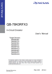
User’s Manual
QB-78K0SKX1
In-Circuit Emulator
Target Devices
78K0S/KU1+
78K0S/KY1+
78K0S/KA1+
78K0S/KB1+
Document No. U18219EJ3V0UM00 (3rd edition)
Date Published June 2007 NS
© NEC Electronics Corporation 2006
Printed in Japan
[MEMO]
2
User’s Manual U18219EJ3V0UM
Windows is either a registered trademark or a trademark of Microsoft Corporation in the United States and/or
other countries.
IECUBE is a registered trademark of NEC Electronics Corporation in Japan and Germany.
PC/AT is a trademark of International Business Machines Corporation.
• The information in this document is current as of June, 2007. The information is subject to change
without notice. For actual design-in, refer to the latest publications of NEC Electronics data sheets or
data books, etc., for the most up-to-date specifications of NEC Electronics products. Not all
products and/or types are available in every country. Please check with an NEC Electronics sales
representative for availability and additional information.
• No part of this document may be copied or reproduced in any form or by any means without the prior
written consent of NEC Electronics. NEC Electronics assumes no responsibility for any errors that may
appear in this document.
• NEC Electronics does not assume any liability for infringement of patents, copyrights or other intellectual
property rights of third parties by or arising from the use of NEC Electronics products listed in this document
or any other liability arising from the use of such products. No license, express, implied or otherwise, is
granted under any patents, copyrights or other intellectual property rights of NEC Electronics or others.
• Descriptions of circuits, software and other related information in this document are provided for illustrative
purposes in semiconductor product operation and application examples. The incorporation of these
circuits, software and information in the design of a customer's equipment shall be done under the full
responsibility of the customer. NEC Electronics assumes no responsibility for any losses incurred by
customers or third parties arising from the use of these circuits, software and information.
• While NEC Electronics endeavors to enhance the quality, reliability and safety of NEC Electronics products,
customers agree and acknowledge that the possibility of defects thereof cannot be eliminated entirely. To
minimize risks of damage to property or injury (including death) to persons arising from defects in NEC
Electronics products, customers must incorporate sufficient safety measures in their design, such as
redundancy, fire-containment and anti-failure features.
• NEC Electronics products are classified into the following three quality grades: "Standard", "Special" and
"Specific".
The "Specific" quality grade applies only to NEC Electronics products developed based on a customerdesignated "quality assurance program" for a specific application. The recommended applications of an NEC
Electronics product depend on its quality grade, as indicated below. Customers must check the quality grade of
each NEC Electronics product before using it in a particular application.
"Standard": Computers, office equipment, communications equipment, test and measurement equipment, audio
and visual equipment, home electronic appliances, machine tools, personal electronic equipment
and industrial robots.
"Special": Transportation equipment (automobiles, trains, ships, etc.), traffic control systems, anti-disaster
systems, anti-crime systems, safety equipment and medical equipment (not specifically designed
for life support).
"Specific": Aircraft, aerospace equipment, submersible repeaters, nuclear reactor control systems, life
support systems and medical equipment for life support, etc.
The quality grade of NEC Electronics products is "Standard" unless otherwise expressly specified in NEC
Electronics data sheets or data books, etc. If customers wish to use NEC Electronics products in applications
not intended by NEC Electronics, they must contact an NEC Electronics sales representative in advance to
determine NEC Electronics' willingness to support a given application.
(Note)
(1) "NEC Electronics" as used in this statement means NEC Electronics Corporation and also includes its
majority-owned subsidiaries.
(2) "NEC Electronics products" means any product developed or manufactured by or for NEC Electronics (as
defined above).
M8E 02. 11-1
User’s Manual U18219EJ3V0UM
3
General Precautions for Handling This Product
1. Circumstances not covered by product guarantee
• If the product was disassembled, altered, or repaired by the customer
• If it was dropped, broken, or given another strong shock
• Use at overvoltage, use outside guaranteed temperature range, storing outside guaranteed
temperature range
• If power was turned on while connection to the AC adapter, USB interface cable, or target system
was in an unsatisfactory state
• If the cable of the AC adapter, the USB interface cable, the target cable, the emulation probe, or the
like was bent or pulled excessively
• If an AC adapter other than the supplied product was used
• If the product got wet
• If this product is connected to the target system when there is a potential difference between the
GND of this product and GND of the target system.
• If the connectors or cables are plugged/unplugged while this product is in the power-on state.
• If excessive load is applied to the connectors or sockets (As for handling, please see 2.6 Mounting
and Connecting Connectors).
• If a metal part of the power switch, cooling fan, or another such part comes in contact with an
electrostatic charge.
2. Safety precautions
• If used for a long time, the product may become hot (50°C to 60°C). Be careful of low temperature
burns and other dangers due to the product becoming hot.
• Be careful of electrical shock. There is a danger of electrical shock if the product is used as
described above in 1. Circumstances not covered by product guarantee.
• The AC adapter supplied with the product is exclusively for this product, so do not use it with other
products.
4
User’s Manual U18219EJ3V0UM
INTRODUCTION
Readers
This manual is intended for users who wish to perform debugging using the QB78K0SKX1. The readers of this manual are assumed to be familiar with the device
functions and usage, and to have knowledge of debuggers.
Purpose
This manual is intended to give users an understanding of the basic specifications and
correct usage of the QB-78K0SKX1.
Organization
This manual is divided into the following sections.
• General
• Setup procedure
• Settings at product shipment
• Ristrictions
How to Read This Manual
It is assumed that the readers of this manual have general knowledge in the fields of
electrical engineering, logic circuits, and microcontrollers.
This manual describes the basic setup procedures and how to set switches.
To understand the overall functions and usages of the QB-78K0SKX1
→ Read this manual in the order of the CONTENTS. The mark “<R>” shows major
revised points. The revised points can be easily searched by copying an “<R>” in
the PDF file and specifying it in the “Find what:” field.
To know the manipulations, command functions, and other software-related settings
of the QB-78K0SKX1
→ See the user’s manual of the debugger (supplied with the QB-78K0SKX1) to be
used.
Conventions
Note:
Footnote for item marked with Note in the text
Caution:
Information requiring particular attention
Remark:
Supplementary information
Numeric representation:
Binary ... xxxx or xxxxB
Decimal ... xxxx
Hexadecimal ... xxxxH
Prefix indicating power of 2
(address space, memory
capacity):
K (kilo): 210 = 1,024
M (mega): 220 = 1,0242
User’s Manual U18219EJ3V0UM
5
Terminology
The meanings of the terms used in this manual are described in the table below.
Term
Meaning
Target device
This is the device to be emulated.
Target system
This is the system to be debugged.
This includes the target program and the hardware provided by the user.
78K0S/Kx1+
Generic name indicating 78K0S/KU1+, 78K0S/KY1+, 78K0S/KA1+, and
78K0S/KB1+.
IECUBE
TM
Generic name for NEC Electronics’ high-performance/compact in-circuit
emulator.
Related Documents
Please use the following documents in conjunction with this manual.
The related documents listed below may include preliminary versions. However,
preliminary versions are not marked as such.
Documents Related to Development Tools (User’s Manuals)
Document Name
QB-78K0SKX1 In-Circuit Emulator
RA78K0S Ver. 2.00 Assembler Package
CC78K0S Ver. 2.00 C Compiler
ID78K0S-QB Ver. 3.00 Integrated Debugger
This manual
Operation
U17391E
Language
U17390E
Structured Assembler Language
U17389E
Operation
U17416E
Language
U17415E
Operation
U18493E
PM plus Ver. 6.30
Caution
U18416E
The related documents listed above are subject to change without notice. Be sure to use the latest
version of each document for designing, etc.
6
Document Number
User’s Manual U18219EJ3V0UM
CONTENTS
CHAPTER 1 GENERAL .............................................................................................................................8
1.1
Hardware Specifications..................................................................................................................................9
1.2
System Specifications ...................................................................................................................................10
1.3
System Configuration ....................................................................................................................................11
1.4
System Configuration for Each Target Device ............................................................................................12
1.5
Package Contents ..........................................................................................................................................13
CHAPTER 2 SETUP PROCEDURE........................................................................................................14
2. 1 Names and Functions of Hardware ...............................................................................................................15
2. 2 Removal of Acrylic Board..............................................................................................................................17
2. 3 Clock Settings ................................................................................................................................................17
2.3.1 Overview of clock settings ..................................................................................................................17
2.3.2 How to set system clock......................................................................................................................18
2.3.3 How to set internal high-speed oscillation clock ..............................................................................20
2.3.4 Internal low-speed oscillation clock ...................................................................................................20
2. 4 Target Device Settings...................................................................................................................................21
2. 5 Software Settings ...........................................................................................................................................21
2. 6 Mounting and Connecting Connectors ........................................................................................................22
2.6.1 Mounting TC to target system.............................................................................................................22
2.6.2 Plugging EA into TC.............................................................................................................................22
2.6.3 Precautions for handling TC ...............................................................................................................23
2. 7 Connecting QB-78K0SKX1 to Target System ..............................................................................................23
2.7.1 When using the emulation probe........................................................................................................23
2.7.2 When using the single-wire target cables ..........................................................................................25
2. 8 Notes on Power Supply and GND Pin Connection......................................................................................28
2. 9 Connecting USB Interface Cable and AC Adapter ......................................................................................28
2. 10 Switching Power On and Off .........................................................................................................................28
CHAPTER 3 SETTINGS AT PRODUCT SHIPMENT ..............................................................................29
CHAPTER 4 RESTRICTIONS ..................................................................................................................30
APPENDIX A CHARACTERISTICS OF TARGET INTERFACE .............................................................32
APPENDIX B REVISION HISTORY .........................................................................................................34
B.1 Major Revisions in This Edition......................................................................................................................34
User’s Manual U18219EJ3V0UM
7
CHAPTER 1
GENERAL
The QB-78K0SKX1 is an in-circuit emulator for emulating the 78K0S/Kx1+.
Hardware and software can be debugged efficiently in the development of systems in which the 78K0S/Kx1+ is
used.
This manual descries basic setup procedures, hardware specifications, system specifications, and how to set
switches.
8
User’s Manual U18219EJ3V0UM
CHAPTER 1
1.1
GENERAL
Hardware Specifications
Table 1-1. QB-78K0SKX1 Hardware Specifications
Parameter
Specification
Target device
78K0S/KU1+, 78K0S/KY1+, 78K0S/KA1+, 78K0S/KB1+
Operating voltage
2.0 to 5.5 V
Operating frequency
system clock
2.7 V ≤ VDD ≤ 5.5 V: 1 to 10 MHz
2.0 V ≤ VDD < 2.7 V: 1 to 5 MHz
Internal high-speed
oscillation clock
An 8 MHz clock (fixed) is supplied from the oscillation circuit in the
QB-78K0SKX1
Internal low-speed
oscillation clock
A 250 kHz clock (fixed) is supplied from the oscillation circuit in the
QB-78K0SKX1
Operating temperature range
0 to 40°C (No condensation)
Storage temperature range
−15 to +60°C (No condensation)
External dimensions
See figure below
Power
consumption
AC adapter for QB-78K0SKX1 Output: DC15 V, 1 A
Input: AC100 to 240 V
Target system power supply
Voltage: 2.0 to 5.5 V
Current: approx. 17 mA MAX.
Weight
Approx. 300 g
Host interface
USB interface
(1.1, 2.0)
108.2 mmNote 2
112.7 mmNote 1
58 mm
Rear spacerNote 3
Front spacerNote 4
Notes 1. Does not include projection of power switch
2. Includes projection of screw that fixes rear spacer
3. Rear spacer can adjust the height from 30 mm (longest) to 0 mm (shortest)
4. Front spacer can adjust the height from 20 mm (longest) to 5 mm (shortest)
User’s Manual U18219EJ3V0UM
9
CHAPTER 1
1.2
GENERAL
System Specifications
This section shows the QB-78K0SKX1 system specifications.
Table 1-2. QB-78K0SKX1 System Specifications
Parameter
Emulation memory capacity
Program execution
functions
Specification
Internal ROM
8 KB (MAX.)
Internal RAM
256 KB (MAX.)
Real-time execution function
Go, Start from Here, Come Here, Restart, Return Out,
Ignore break points and Go
Non-real-time execution function
Step In, Next Over, Slowmotion, Go & Go
Memory manipulation
Available (initialize, copy, compare)
Register manipulation
Available (general-purpose registers, control registers, SFRs)
Disassemble function
Available
Local variable view
Local variables
Watch data view
Local variables, global variables, or else
Stack trace view
Available
Break functions
Trace functions
Event break
Access: 1 point
Software break
2000 points
Other
Forcible break
Trace data types
Program address, program data
Trace modes
Unconditional instruction branch trace
Trace functions
Non-stop
Memory capacity
1 K frames
Pseudo-real-time RAM monitoring function
All internal RAM spaces (16 bytes)
Time measurement
functions
Measurement clock
8 MHz
Measurement objects
Start through end of program execution
Maximum measurement time
Approx. 1 hour and 12 minutes (Resolution: 125 ns)
Number of timers for
measurement
Start through end of program execution: 1
Measurement results
Execution time (start through end of execution)
Other functions
Command functions set in the console
Event function, power-off emulation function, pin mask function,
flash self programming emulation function
Table 1-3.
List of QB-78K0SKX1 Peripheral Break Functions
Parameter
Peripheral Break: Peripheral function which
stops when Break is set
Target Peripheral Function Name
16-bit timer/event counter 00
8-bit timer 80
8-bit timer H1
10
User’s Manual U18219EJ3V0UM
CHAPTER 1
1.3
GENERAL
System Configuration
This section shows the system configuration when using the QB-78K0SKX1 connected to a PC (Windows
TM
(Windows 98 SE or later), PC/AT
compatible).
TM
PC
Connection is possible even without optional products.
Figure 1-1. System Configuration
<1> Host machine
<2> ID78K0S-QB Disk/Accessory Disk
<3> USB interface cable
<4> AC adapter
<5> QB-78K0SKX1
<6> Emulation probe
<7> Exchange adapter
<8> Target connector
<9> Target cables (30 single-wire cables)
<10> Target system (device foot pattern)
<11> Target system (pin header)
: Windows PC (Windows 98 SE or later), IBM PC/AT compatible can be
used
: Debugger, USB drivers, manual, etc.
: Cable connecting QB-78K0SKX1 to host machine
: Support input AC100 to 240 V
: This product
: Flexible type emulation probe
: Adapter that performs pin conversion
flexible type for 10-pin and 16-pin
board type for 20-pin and 30-pin
: Connector soldered to target system
: Recommended specification
vertical 0.635 mm, horizontal 0.635 mm, height 6 mm
Remarks 1. Obtain device files from the NEC Electronics Microcontrollers and Microprocessors website.
http://www.necel.com/micro/ods/eng/index.html
2. Refer to 1.5 Package Contents for the purchase forms of the above products.
3. As for handling of connectors, refer to 2.6 Mounting and Connecting Connectors.
User’s Manual U18219EJ3V0UM
11
CHAPTER 1
1.4
GENERAL
System Configuration for Each Target Device
The following table lists the system configuration for each target device of the QB-78K0SKX1.
Table 1-4. Adapters and Connectors for Each Target Device
Target Device
78K0S/KU1+
Exchange Adaptor
Target Connector
QB-10MA-EA-01T
Note 2
(sold separately)
QB-10MA-NQ-01T
Note 2
(sold separately)
Note 1
16-pin GR
QB-16GR-EA-01T
Note 2
(sold separately)
QB-16GR-NQ-01T
Note 2
(sold separately)
78K0S/KA1+
Note 1
20-pin MC
QB-20MC-EA-01T
Note 2
(sold separately)
QB-20MC-NQ-01T
Note 2
(sold separately)
78K0S/KB1+
Note 1
30-pin MC
QB-30MC-EA-04T
Note 2
(sold separately)
QB-30MC-NQ-02T
Note 2
(sold separately)
78K0S/KY1+
<R>
Package
10-pin MA
Table 1-5. Common Probe
Name
Part Number
Note 2
Emulation probe
QB-50-EP-01T (sold separately)
<R> Notes 1. To develop WLBGA or SDIP, use the attached target cable (single-wire). Refer to 2.7.2 When using the
single-wire target cables.
2.
These items are included with the QB-78K0SKX1, depending on the ordering code.
• If QB-78K0SKX1-ZZZ is ordered
The emulation probe, exchange adapter, and target connector are not included.
• If QB-78K0SKX1-T10MA is ordered
The QB-50-EP-01T, QB-10MA-EA-01T, and QB-10MA-NQ-01T are included.
• If QB-78K0SKX1-T16GR is ordered
The QB-50-EP-01T, QB-16GR-EA-01T, and QB-16GR-NQ-01T are included.
• If QB-78K0SKX1-T20MC is ordered
The QB-50-EP-01T, QB-20MC-EA-01T, and QB-20MC-NQ-01T are included.
• If QB-78K0SKX1-T30MC is ordered
The QB-50-EP-01T, QB-30MC-EA-04T, and QB-30MC-NQ-02T are included.
Remark For notes on target system design and package drawings, refer to [Related Information] on the following
URL.
http://www.necel.com/micro/english/iecube/index.html
12
User’s Manual U18219EJ3V0UM
CHAPTER 1
1.5
GENERAL
Package Contents
The following items have been placed in the QB-78K0SKX1 packing box.
Please check the contents.
Products supplied with QB-78K0SKX1-ZZZ
1:
QB-78K0SKX1
2:
AC adapter
3:
USB interface cable (2 meters)
4:
Target cable (30 single-wire cables)
5:
Online user registration card (warranty card and software contract in one)
6:
ID78K0S-QB Disk (CD-ROM)
7:
Accessory Disk (CD-ROM)
8:
IECUBE Setup Manual (Japanese/English)
9:
Pin header cover for QB-78K0SKX1 (Japanese/English)
10:
Packing list
11:
Simple programmer (QB-MINI2)
Products supplied with QB-78K0SKX1-T10MA
1 to 11
12:
Emulation probe
13:
Exchange adapter
14:
Target connector
QB-50-EP-01T
QB-10MA-EA-01T
QB-10MA-NQ-01T
Products supplied with QB-78K0SKX1-T16GR
1 to 11
12:
Emulation probe
13:
Exchange adapter
14:
Target connector
QB-50-EP-01T
QB-16GR-EA-01T
QB-16GR-NQ-01T
Products supplied with QB-78K0SKX1-T20MC
1 to 11
12:
Emulation probe
13:
Exchange adapter
14:
Target connector
QB-50-EP-01T
QB-20MC-EA-01T
QB-20MC-NQ-01T
Products supplied with QB-78K0SKX1-T30MC
1 to 11
12:
Emulation probe
13:
Exchange adapter
14:
Target connector
QB-50-EP-01T
QB-30MC-EA-04T
QB-30MC-NQ-02T
User’s Manual U18219EJ3V0UM
13
CHAPTER
2
SETUP
PROCEDURE
This chapter explains the QB-78K0SKX1 setup procedure.
Setup can be completed by performing installation setup in the order in which it appears in this chapter.
Perform setup along the lines of the following procedure.
See 2.1 Names and Functions of Hardware for clock positions.
Clock settings
Hardware settings are not required if the clock internally generated from the QB-78K0SKX1 is used.
If an oscillator must be mounted, see 2.2
Removal of Acrylic Board and 2.3
Clock Settings.
Target device settings
At shipment, the QB-78K0SKX1 is set to perform as the 78K0S/KA1+ or 78K0S/KB1+.
To emulate the performance of the 78K0S/KU1+ or 78K0S/KY1+, See 2.4
Power switch
See 2.5
Software settings.
Mounting and connecting connectors
See 2.6
Mounting and Connecting Connectors.
Connecting QB-78K0SKX1 to target system
See 2.7
Connecting QB-78K0SKX1 to Target System.
Connecting USB interface cable and AC adapter
See 2.9
Connecting USB Interface Cable and AC Adapter.
Switching power on and off
See 2.10
14
Switching Power On and Off.
User’s Manual
U18219EJ3V0UM
Target Device Settings.
CHAPTER
2. 1
2
SETUP
PROCEDURE
Names and Functions of Hardware
Figure 2-1. Names of Parts of QB-78K0SKX1
Top View
Bottom View
CN7
SW1
Power switch
JP1
CN5
POWER
Power switch
OSC1
TARGET
Power supply connector
Side View
USB connector
Note
40-pin 2.54 mm pitch connector
Note
Pin 20 (N.C.) is a disconnected pin by default (at shipment).
User’s Manual
U18219EJ3V0UM
15
CHAPTER
2
SETUP
PROCEDURE
(1) CN7
This is a connector for connecting an emulation probe.
(2) 40-pin 2.54 mm pitch connecter
This is a connector for connecting target cables (30 single-wire cables).
(3) SW1
This is a target device selection switch. The switch is set to use the 78K0S/KA1+ or 78K0S/KB1+ at
shipment.
(4) OSC1
This is a socket for mounting the oscillator.
(5) CN5
This is a connector for the shipment inspection. It is not intended for users to use.
(6) POWER (Red LED)
This is an LED that shows whether the power supply of the QB-78K0SKX1 is switched on.
LED State
QB-78K0SKX1 State
Lit
Power switch ON
Not lit
Power switch OFF or AC adapter not connected to QB-78K0SKX1
Blinking
Internal error occurred (Contact an NEC Electronics sales representative or distributor)
(7) TARGET (Green LED)
This is an LED that shows whether the power supply of the target system is switched on.
LED State
Target System State
Lit
Target system power supply ON
Not lit
Target system power supply OFF or target system not connected
(8) Power switch
This is the power switch of the QB-78K0SKX1.
It is OFF at shipment.
(9) JP1
This is a jumper for the shipment inspection.
At shipment, it is set as 1-2, 3-4 and 5-6 short. The settings other than this are prohibited.
16
User’s Manual
U18219EJ3V0UM
CHAPTER
2
SETUP
PROCEDURE
2. 2 Removal of Acrylic Board
To modify the clock setting, the acrylic board on the bottom of the QB-78K0SKX1 must be removed.
The acrylic board can be removed by lifting it up.
Figure 2-2. Acrylic Board Removal Method
2. 3 Clock Settings
2.3.1
Overview of clock settings
The following four types of clock settings are available.
Each clock setting is listed below.
Table 2-1. Clock Settings
<R>
Clock Used
System clock
Internal high-speed oscillation clock
Clock Supply
Debugger Setting
(in Configuration
Dialog Box)
Uses the clock internally generated from the QB-78K0SKX1
System (5.00, 8.00,
10.00 [MHz])
Uses the clock generated from the oscillator (OSC1) mounted
on the QB-78K0SKX1
Clock Socket
Uses the clock internally generated from the QB-78K0SKX1
System (None)
Internal low-speed oscillation clock
–
The clock to be used is selected depending on the setting of the option byte.
To select crystal/ceramic oscillation circuit or external clock input circuit, see 2.3.2 How to set system clock.
<R>
When the internal high-speed oscillation clock is selected, see 2.3.3 How to set internal high-speed oscillation
clock.
Oscillation with the resonator on the target system and an external input clock are not supported.
<R>
Remark
If an oscillation circuit having an oscillator or resonator is mounted in OSC1, “Clock Socket” is
automatically selected, thus “System” is not available.
User’s Manual
U18219EJ3V0UM
17
CHAPTER
2.3.2
2
SETUP
PROCEDURE
How to set system clock
The clock settings are listed below.
Table 2-2. Settings for System Clock
Type of Clock to Be Used
<R>
OSC1
(1) Using the clock internally generated from the QB-78K0SKX1
Nothing is mounted
Debugger Setting
System (5.00, 8.00, 10.00
[MHz])
(2) Using the oscillation circuit (OSC1), having an oscillator or
resonator, mounted on the QB-78K0SKX1
The oscillation circuit having an
Clock Socket
oscillator or resonator is mounted
<R>
Remarks 1. If “None” is selected without the internal high-speed oscillation clock being selected by the
<R>
2. If an oscillation circuit having an oscillator or resonator is mounted in OSC1, “Clock Socket”
option byte setting, the CPU operates at 8.00 MHz.
is automatically selected.
(1) Using the clock internally generated from the QB-78K0SKX1
Select the “System” in the debugger and select the desired frequency from the drop-down list.
The following frequencies are selectable.
5.00, 8.00, 10.00 [MHz]
(2) Using the oscillation circuit (OSC1), having an oscillator or resonator, mounted on the QB-78K0SKX1
OSC1 of the QB-78K0SMINI does not mount an oscillator or an oscillation circuit at shipment.
OSC1
specifications are shown in (a) to (d) of Figure 2-3.
Note that an oscillation circuit can also be configured by mounting a parts board such as the
160-90-314 (product of PRECI-DIP) in OSC1.
The capacitors and resistors mounted on the parts
board should be used at the constants recommended by the resonator manufacturer.
A diagram of the
parts board mounted in OSC1 is shown in (e) of Figure 2-3.
Caution
Be sure to mount the clock on and remove it from OSC1 with the power supply of the
QB-78K0SKX1 switched off.
18
User’s Manual
U18219EJ3V0UM
CHAPTER
2
SETUP
Figure 2-3.
PROCEDURE
Using Oscillator
(a) Equivalent circuit
(b) Mounted parts
1 MΩ
HCU04
5
Rx
10
4
3
CA
12
Pin Number
HCU04
98
CLOCK OUT
11
13
CB
2
(c) Example of mounting parts board (oscillator
Connected Part
2-13
Capacitor CB
3-12
Capacitor CA
4-11
Ceramic resonator/crystal resonator
5-10
Resistor RX
8-9
Shorted
(d) Supported oscillator pin assignment
circuit parts)
1
14
2
13
3
12
4
11
5
10
6
9
7
8
14 VCC
NC 1
8 CLOCK OUT
GND 7
Top view
Top view
(e) Parts board mounted in OSC1
Mount an oscillator in OSC1 in the QB-78K0SKX1 and then select the “Clock socket” in the debugger.
The clock generated from the oscillator mounted on the QB-78K0SKX1 is used.
The selectable frequencies are same as those of the target device.
User’s Manual
U18219EJ3V0UM
19
CHAPTER
2
SETUP
PROCEDURE
As an oscillator to be mounted in OSC1 in the QB-78K0SKX1, use the one that satisfies the following
specifications.
- Supply voltage: 5 V
- Output level: CMOS
Figure 2-4. Mapping of Oscillator to OSC1
Oscillator
Top view
Socket
VCC
NC
GND
CLOCK OUT
Oscillator Pin
OSC1 Pin Number
NC
1
12
GND
7
4
11
CLOCK OUT
8
5
10
VCC
14
6
9
7
8
1
14
2
13
3
Remark Watch out for the pin 1 position and insert the oscillator into the socket.
<R> 2.3.3 How to set internal high-speed oscillation clock
Select “System” in the debugger and select “None” from the drop-down list.
By the setting of the option byte, 8 MHz from the oscillation circuit in the QB-78K0SKX1 is used.
Figure 2-5.
Debugger Configuration Dialog Box Setting
RemarkIf the internal high-speed oscillation clock is selected by the option byte setting without selecting “None”, the
CPU operates at 8.00 MHz after reset.
2.3.4
Internal low-speed oscillation clock
The debugger setting is not necessary.
250 MHz from the oscillation circuit in the QB-78K0SKX1 is used.
20
User’s Manual
U18219EJ3V0UM
CHAPTER
2
SETUP
PROCEDURE
2. 4 Target Device Settings
The target device is set by using SW1 on the QB-78K0SKX1.
When emulating the 78K0S/KA1+ or 78K0S/KB1+: Set to KA1+/KB1+ side
When emulating the 78K0S/KU1+ or 78K0S/KY1+: Set to KU1+/KY1+ side
Figure 2-6. SW1 Setting
Caution
When using the 78K0S/KA1+
When using the 78K0S/KU1+
or 78K0S/KB1+
or 78K0S/KY1+
KA1+/KB1+
KA1+/KB1+
KU1+/KY1+
KU1+/KY1+
Be sure to switch off the power supply of the QB-78K0SKX1 before changing the setting.
2. 5 Software Settings
For details, see the ID78K0S-QB Ver. 3.00 Integrated Debugger Operation User's Manual (U18493E).
User’s Manual
U18219EJ3V0UM
21
CHAPTER
2
SETUP
PROCEDURE
2. 6 Mounting and Connecting Connectors
This section describes the methods of connecting the target connector and exchange adapter to target system.
Make connections with both the power supplies of the QB-78K0SKX1 and target system switched off.
The following abbreviations are used in this section:
- TC: Target connector
- EA: Exchange adapter
2.6.1
Mounting TC to target system
(1) Thinly apply an adhesive to the back of the TC and adhere the TC to the target system.
In addition, be sure
to clean the back of the TC as well as the surface of the target system using alcohol or the like.
Align the TC
leads along the target system pads .
(2) Preserve the soldering conditions (use Sn-3.5Ag-0.5Cu) and solder carefully to prevent troubles such as flux
or solder splashing and adhering to the contact pins.
Solder reflow:
Preheating: 150 to 170°C
120 seconds or less
Heating: 220°C
60 seconds or less
Maximum temperature: 240°C or below
The above profile represents the temperature around the
soldering pins.
Manual soldering:
350°C × 5 seconds or less (1 pin)
2.6.2
Plugging EA into TC
Check the pin 1 position of the EA and the pin 1 mark (silk) of the pin 1 position of the TC and plug in.
22
User’s Manual
U18219EJ3V0UM
CHAPTER
2.6.3
2
SETUP
PROCEDURE
Precautions for handling TC
(1) Do not perform cleaning by flux immersion or vapor.
(2) Prying at insertion/removal might break the connector, therefore be sure to insert/remove vertically.
(3) This system cannot be used in an environment of vibrations or shocks.
(4) It is assumed that this product will be used in system development and evaluation. Moreover, when used in
Japan, Electrical Appliance and Material Control Law and electromagnetic disturbance countermeasures
have not been applied.
(5) Since there are cases of shape change if the packing case is left for a long time in a place where it is 50°C
or higher, for safekeeping, store it in a place where it is no higher than 40°C and direct sunlight does not hit
it.
2. 7 Connecting QB-78K0SKX1 to Target System
2.7.1
When using the emulation probe
If connecting the emulation probe (QB-50-EP-01T), connect it to the QB-78K0SKX1 and the target system by the
following procedure.
(a) Connecting the emulation probe
Connect the emulation probe to the QB-78K0SKX1.
Figure 2-7. Using the Emulation Probe
Insert matching CN7 of the QB-78K0SKX1
and CN1 of the probe
User’s Manual
U18219EJ3V0UM
23
CHAPTER
2
SETUP
PROCEDURE
(b) Ensuring isolation
When connecting the target system to the QB-78K0SKX1 using the emulation probe, perform height
regulation using the front spacer or rear spacer of the QB-78K0SKX1 and ensure isolation from the
target system.
Figure 2-8. Connection Using the Emulation Probe
Rear spacer
(height-adjustable)
Emulation probe
Front spacer
(height-adjustable)
Exchange adapter
Target connector
(c) Precautions related to emulation probe
Be careful that stress of the emulation probe is not placed on the target connector.
Moreover, when
removing the emulation probe, remove it slowly while pressing down on the exchange adapter with a
finger so that there is no stress on the target connector.
24
User’s Manual
U18219EJ3V0UM
CHAPTER
2.7.2
2
SETUP
PROCEDURE
When using the single-wire target cables
Connect the QB-78K0SKX1 to the target system using the target cable (supplied), etc.
The 40-pin 2.54 mm pitch connecter of the QB-78K0SKX1 incorporates a male pin header, so be sure to mount a
male pin header on the target system connector.
Connect corresponding pins to each other using a target cable with
female connectors on each end.
• Specifications of target cables (single-wire cables)
Red: 250 mm cable for power supply line (connected to VDD and AVREF pins) × 2
Black: 250 mm cable for GND line (connected to VSS and AVSS pins) × 2
Yellow: 250 mm cable for general signals × 26
• Specifications of target system pin header:
0.635 mm × 0.635 mm (height: 6 mm)
When mounting the pin header, ensure that the pin pitch is at least 2.54 mm.
The 40-pin 2.54 mm pitch connecter of the QB-78K0SKX1 incorporates a 40-pin pin header, so by mounting an
IDE connector on the target system, the QB-78K0SKX1 can also be connected to the target system using a
commercial IDE cable (ATA33 standard).
The pins in the 40-pin 2.54 mm pitch connecter correspond functionally to the pins of the target device (pins 10, 16,
20, and 30).
The functions of the target device pins can be switched using the target device selection switch (SW1).
The attached product “Pin header cover for QB-78K0SKX1” that indicates the signal name of the target device pins is
provided.
Use the appropriate cover by cutting it off from the product along the lines with scissors or a cutter, and cover the
side of the QB-78K0SKX1 with it.
Cautions 1. Be careful not to hurt yourself with scissors or a cutter when cutting off the “Pin header
cover for QB-78K0SKX1”.
2. When emulating products other than the 78K0S/KB1+, do not connect anything to the target
I/F (pin header) pins that have not been assigned any pin functions (unused pins).
User’s Manual
U18219EJ3V0UM
25
CHAPTER
2
SETUP
PROCEDURE
Figure 2-9. Connection of QB-78K0SKX1 (40-pin 2.54 mm pitch connecter) to Target System
Connect the 40-pin 2.54 mm pitch connecter on the QB-78K0SKX1 to the target board connector using the target
cables in accordance with the pin assignment of the target device.
Be sure that both the power supplies of the target
system and QB-78K0SKX1 are switched off.
26
User’s Manual
U18219EJ3V0UM
CHAPTER
2
SETUP
PROCEDURE
Table 2-3. Pin Correspondence
Pin No.
Target Device Setting
KU1+/KY1+ Mode
KA1+/KB1+ Mode
78K0S/KU1+ (10 Pins)
78K0S/KY1+ (16 Pins)
1
−
−
2
−
−
78K0S/KA1+ (20 Pins)
AVREF(20)
78K0S/KB1+ (30 Pins)
AVREF(28)
−
AVSS(29)
3
P20/ANI0/TI000/TOH1(1)
P20/ANI0/TI000/TOH1(1)
P20/ANI0(19)
P20/ANI0(27)
4
GND
GND
GND
GND
5
P21/ANI1/TI010/TO/INTP0(10) P21/ANI1/TI010/TO/INTP0(16) P21/ANI1(18)
P21/ANI1(26)
6
GND
GND
GND
GND
7
P22/X2/ANI2(6)
P22/X2/ANI2(9)
P22/ANI2(17)
P22/ANI2(25)
8
GND
GND
GND
GND
9
P23/X1/ANI3(5)
P23/X1/ANI3(8)
P23/ANI3(16)
P23/ANI3(24)
10
GND
GND
GND
GND
11
VDD(4)
VDD(5)
VDD(5)
VDD(7)
12
VSS(3)
VSS(4)
VSS(1)
VSS(6)
−
13
14
GND
GND
−
15
16
GND
GND
GND
−
N.C.
−
P40(2)
−
24
−
25
−
26
−
P43(9)
GND
P121/X1(2)
P121/X1(8)
GND
GND
P122/X2(3)
P122/X2(9)
GND
GND
P123(4)
P123(5)
N.C.
N.C.
−
P00(4)
−
P01(3)
P40(9)
P41(2)
P40(15)
P41/INTP3(10)
−
P42(15)
−
P42/TOH1(11)
−
P43(14)
P41/INTP3(16)
P02(2)
P42/TOH1(17)
−
P03(1)
P43/TxD6/INTP1(12)
P43/TxD6/INTP1(18)
P130(15)
P130(23)
29
−
30
−
31
−
32
−
33
−
34
−
P46(7)
P32/INTP1(13)
−
P32(12)
36
−
P47(6)
−
P47(22)
37
−
−
P33(11)
35
P32/INTP1(8)
−
P120(30)
GND
−
−
27
−
−
P40(3)
23
28
−
N.C.
21
22
−
GND
19
20
−
−
17
18
−
P44(11)
P44/RxD6(13)
P44/RxD6(19)
−
P30/TI000/INTP0(8)
P30/TI000/INTP0(14)
P45(14)
P45(20)
−
P31/TI010/TO00/INTP2(7)
P31/TI010/TO00/INTP2(13)
P45(10)
−
−
P46(21)
38
GND
GND
GND
GND
39
P34/RESET(7)
P34/ RESET(12)
P34/RESET(6)
P34/RESET(10)
40
GND
GND
GND
GND
Remark
−: Pins not required in target device
(
GND:
Connected to VSS (pin 12) on the QB-78K0SKX1
): The number in the parentheses indicates the pin number in the target device.
User’s Manual
U18219EJ3V0UM
27
CHAPTER
2
SETUP
PROCEDURE
2. 8 Notes on Power Supply and GND Pin Connection
Be sure to connect all the power supplies and GND pins of the target device to each power supply or GND of the
QB-78K0SKX1.
2. 9 Connecting USB Interface Cable and AC Adapter
Plug the USB interface cable supplied with the QB-78K0SKX1 into the USB connector of the host machine, and
plug the other side into the USB connector on the rear of the QB-78K0SKX1.
Plug the AC adapter supplied with the QB-78K0SKX1 into a receptacle and plug the other side into the power
supply connector on the rear of the QB-78K0SKX1.
For QB-78K0SKX1 connector positions, see Figure 2-10.
Figure 2-10. Connector Positions
Power supply connector
(Connect AC adapter)
USB connector
(Connect USB interface cable)
2. 10 Switching Power On and Off
Be sure to switch the power on and off according to the following procedures.
- Switching power on
- Switching power off
<1> QB-78K0SKX1 power switch ON
<2> Target system power switch ON
<3> Debugger startup
<1> Debugger termination
Note
Note
<2> Target system power switch OFF
<3> QB-78K0SKX1 power switch OFF
Note <2> is unnecessary if the target system is not connected.
Caution
If the wrong sequence was used for the operation, the target system or the QB-78K0SKX1 may
fail.
28
User’s Manual
U18219EJ3V0UM
CHAPTER 3
SETTINGS AT PRODUCT SHIPMENT
Table 3-1. Settings at Shipment
Item
JP1
Setting
2
Remarks
6
Set as 1-2, 3-4 and 5-6 short.
Do not change the settings.
1
OSC1
5
Oscillation
Not mounted
circuit
using
an
oscillator
or
resonator can be mounted.
SW1
KA1+/KB1+
Target device selection switch.
Set to use the 78K0S/KA1+ or 78K0S/KB1+ at
shipment.
KU1+/KY1+
Power switch
Set to OFF at shipment.
User’s Manual
U18219EJ3V0UM
29
CHAPTER 4 RESTRICTIONS
The following restrictions apply to the QB-78K0SKX1.
{ Clock oscillation or clock input via a resonator on the target system is not supported. The clock differs between
the device and the tool (QB-78K0SKX1) according to the option byte (OSCSEL1, OSCSEL0) setting as follows.
When the target device is other than the µPD78F950x
Device
Option Byte
Tool
OSCSEL1
OSCSEL0
0
0
Crystal/ceramic oscillation clock
System clock on QB-78K0SKX1
0
1
External clock input
System clock on QB-78K0SKX1
1
x
Internal high-speed oscillation clock
Internal high-speed oscillation clock of QB-78K0SKX1
When the target device is the µPD78F950x
Device
Option Byte
Tool
OSCSEL1
OSCSEL0
0
0
Internal high-speed oscillation clock
System clock on QB-78K0SKX1
0
1
External clock input
System clock on QB-78K0SKX1
1
x
Internal high-speed oscillation clock
Internal high-speed oscillation clock of QB-78K0SKX1
Note
Note If OSCSEL1 and 0 are set to 0 and 0, set the setting in the Configuration dialog box of the debugger to
“None” or “8 MHz”.
{ The oscillation circuit on the QB-78K0SKX1 generates a 250 kHz clock as the internal low-speed oscillation
clock, and an 8 MHz clock as the internal high-speed oscillation clock. Note that the clock characteristics differ
from those of the target device.
{ The QB-78K0SKX1 has 256 KB of RAM. However, unfortunately the 256 KB RAM area can be accessed
normally from the user program even when a 128 KB device is being emulated, so be aware that problems
such as stack overflow may occur unnoticed.
{ The characteristics of the A/D converter, LVI, and ports are not fully equivalent to those of the device.
Moreover, pull-down resistors have also been inserted at the port signals to protect the target interface. See
APPENDIX A CHARACTERISTICS OF TARGET INTERFACE for details.
{ AVSS and VSS are equivalent on the QB-78K0SKX1.
{ When using the QB-78K0SKX1, a correct A/D conversion result can be obtained even without waiting for 1 µs
to elapse after setting bit 0 (ADCE) of the A/D converter mode register (ADM) to 1. When using the actual
device, however, be sure to execute processing such as reading and discarding this result.
{ The internal functions (registers, peripheral macro, multiplier, etc.) of the QB-78K0SKX1 always operate for the
78K0S/KB1+. Therefore, while the emulation is performed for the 78K0S/KA1+, KU1+, or KY1+, if the bit of the
register which exists only in the 78K0S/KB1+ is accessed from the program, it can be read or written even if
access to the bit is disabled under normal conditions. In addition, the multiplication instruction execution can
also be enabled while the emulation is performed for the 78K0S/KA1+, KU1+, or KY1+.
30
User’s Manual U18219EJ3V0UM
CHAPTER 4 RESTRICTIONS
{ Device file versions
Use the combinations that satisfy the table below.
The device files can be downloaded from the following page on NEC Electronics Microcontrollers and
Microprocessors website.
URL: http://www.necel.com/micro/ods/eng/index.html → Version-up Service
Target Device
Control Code
Usable Device File
78K0S/KA1+: µPD78F9221, 78F9222
A or later
DF789222 V2.00 or DF789234 V2.00 or later
78K0S/KU1+: µPD78F9200, 78F9201, 78F9202
A or later
DF789234 V2.11 or later
User’s Manual U18219EJ3V0UM
31
APPENDIX A
CHARACTERISTICS OF TARGET INTERFACE
This chapter explains the differences between the signal lines of the target interface circuit of the QB-78K0SKX1
and the signal lines of the target device.
Although the target device is a CMOS circuit, the target interface circuit of the QB-78K0SKX1 consists of an
emulation circuit that depends on the emulation CPU, TTL, CMOS-IC, etc.
When the target system is debugged by connecting it to the QB-78K0SKX1, the QB-78K0SKX1 emulates just as if
the actual target device were operating on the target system.
However, small differences arise because the QB-78K0SKX1 actually is emulating.
The target interface equivalent circuit of the QB-78K0SKX1 is shown in Figure A-1.
Figure A-1. Equivalent Circuit (1/2)
Target system side
QB-78K0SKX1 side
Same voltage as VDD
µPD7886
(Voltage level shifter)
VDDB
33 kΩ
P00 to 03
P30 to 33
P40 to 47
P120, 123
(Pull-up
B resistor
option)
A
(Port functions,
B
A
etc)
1 MΩ
µPD7886
(Voltage level shifter)
VDDB
32
XC3S1000
(FPGA)
VDDA
Same voltage as VDD
P34
P121, 122
P130
3.3 V
3.3 V
VDDA
XC3S1000
(FPGA)
(Port functions,
B
A
etc)
1 MΩ
User’s Manual
U18219EJ3V0UM
APPENDIX A
CHARACTERISTICS OF TARGET INTERFACE
Figure A-1. Equivalent Circuit (2/2)
Target system side
QB-78K0SKX1 side
Same voltage as AVREF
µPD7886
(Voltage level shifter)
74HCT
4066
(PORT)
P20 to 23
33 kΩ
3.3 V
VDDB
VDDA
(Port functions,
B
A
etc)
XC3S1000
(FPGA)
1 MΩ
74HCT
4066
(Pull up)
B
(Pull-up
resistor
option)
A
Same voltage as AVREF
74HCT
4066
(AN In)
AD7813YR
(A/D converter)
33 pF
Same voltage as VDD
VDD
NFE31PT222Z1E9L
(Filter)
4.3 kΩ
Target power
supply detection
10 kΩ
Same voltage as VDD
Same voltage as AVREF
SW1
AVREF
NFE31PT222Z1E9L
(Filter)
100 kΩ
SW1
KU1+/KY1+
KA1+/KB1+
VSS
AVSS
User’s Manual
U18219EJ3V0UM
33
APPENDIX B REVISION HISTORY
B.1 Major Revisions in This Edition
Page
Description
CHAPTER 1 GENERAL
p.12
Change of Table 1-4. Adapters and Connectors for Each Target Device
B.2 Revision History of Preceding Editions
Edition
2nd
Description
Addition of Note 1 to “78K0S/KA1+” in Table 1-4. Adapters and Connectors for
Each Target Device
Chapter
CHAPTER 1 GENERAL
Change of Remark of 1.4 System Configuration for Each Target Device
Change of Table 2-1. Clock Settings
Change of description of and addition of Remark to 2.3.1 Overview of clock
settings
CHAPTER 2 SETUP
PROCEDURE
Change of Table 2-2. Settings for System Clock, figure, and Remarks 1 and 2
Change of description of and addition of Figure 2-5 and Remark to 2.3.3 How to set
internal high-speed oscillation clock
34
Change and addition of description
CHAPTER 4
RESTRICTIONS
Deletion of chapter
APPENDIX B
PACKAGE DRAWINGS
in 1st edition
Addition of APPENDIX B REVISION HISTORY
APPENDIX B
REVISION HISTORY
User’s Manual U18219EJ3V0UM
For further information,
please contact:
NEC Electronics Corporation
1753, Shimonumabe, Nakahara-ku,
Kawasaki, Kanagawa 211-8668,
Japan
Tel: 044-435-5111
http://www.necel.com/
[America]
[Europe]
[Asia & Oceania]
NEC Electronics America, Inc.
2880 Scott Blvd.
Santa Clara, CA 95050-2554, U.S.A.
Tel: 408-588-6000
800-366-9782
http://www.am.necel.com/
NEC Electronics (Europe) GmbH
Arcadiastrasse 10
40472 Düsseldorf, Germany
Tel: 0211-65030
http://www.eu.necel.com/
NEC Electronics (China) Co., Ltd
7th Floor, Quantum Plaza, No. 27 ZhiChunLu Haidian
District, Beijing 100083, P.R.China
Tel: 010-8235-1155
http://www.cn.necel.com/
Hanover Office
Podbielskistrasse 166 B
30177 Hannover
Tel: 0 511 33 40 2-0
Munich Office
Werner-Eckert-Strasse 9
81829 München
Tel: 0 89 92 10 03-0
Stuttgart Office
Industriestrasse 3
70565 Stuttgart
Tel: 0 711 99 01 0-0
United Kingdom Branch
Cygnus House, Sunrise Parkway
Linford Wood, Milton Keynes
MK14 6NP, U.K.
Tel: 01908-691-133
Succursale Française
9, rue Paul Dautier, B.P. 52
78142 Velizy-Villacoublay Cédex
France
Tel: 01-3067-5800
Sucursal en España
Juan Esplandiu, 15
28007 Madrid, Spain
Tel: 091-504-2787
Tyskland Filial
Täby Centrum
Entrance S (7th floor)
18322 Täby, Sweden
Tel: 08 638 72 00
Filiale Italiana
Via Fabio Filzi, 25/A
20124 Milano, Italy
Tel: 02-667541
Shanghai Branch
Room 2509-2510, Bank of China Tower,
200 Yincheng Road Central,
Pudong New Area, Shanghai, P.R.China P.C:200120
Tel:021-5888-5400
http://www.cn.necel.com/
Shenzhen Branch
Unit 01, 39/F, Excellence Times Square Building,
No. 4068 Yi Tian Road, Futian District, Shenzhen,
P.R.China P.C:518048
Tel:0755-8282-9800
http://www.cn.necel.com/
NEC Electronics Hong Kong Ltd.
Unit 1601-1613, 16/F., Tower 2, Grand Century Place,
193 Prince Edward Road West, Mongkok, Kowloon, Hong Kong
Tel: 2886-9318
http://www.hk.necel.com/
NEC Electronics Taiwan Ltd.
7F, No. 363 Fu Shing North Road
Taipei, Taiwan, R. O. C.
Tel: 02-8175-9600
http://www.tw.necel.com/
NEC Electronics Singapore Pte. Ltd.
238A Thomson Road,
#12-08 Novena Square,
Singapore 307684
Tel: 6253-8311
http://www.sg.necel.com/
NEC Electronics Korea Ltd.
11F., Samik Lavied’or Bldg., 720-2,
Yeoksam-Dong, Kangnam-Ku,
Seoul, 135-080, Korea
Tel: 02-558-3737
http://www.kr.necel.com/
Branch The Netherlands
Steijgerweg 6
5616 HS Eindhoven
The Netherlands
Tel: 040 265 40 10
G0706