1
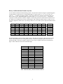
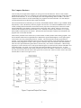
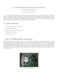
Appendix F The Simon Board Getting Started Use the web browser to open up the web page http://eceweb.mst.edu/courses/Intro/. This page has several links, which we will use later on. Embedded Computers Embedded computers are all around you. They are different from the usual desktop computers in that they don’t look like computers; don’t usually have a keyboard or display like a PC; are usually quite small and inexpensive (cost a few dollars or less and can run on a watch battery); are usually custom made for a specific application; and are essentially invisible (unless you look closely). Table 1 given below shows some differences between the typical PC and the typical embedded computer. Input Output Memory Storage Cost Desktop Computer (PC) Embedded Computer Keyboard, Mouse Switches, Keypad, Sensors Monitor, Printer Control Signals, LED’s, Display, Beeper Megabytes SRAM, BIOS in ROM Kilobytes of ROM (Flash), small amount of RAM Floppy Disk, Hard Disk, CDROM None $1000 <$100 Table 1 Desktop vs. Embedded The control signals are what make embedded computers important. In fact a lot of the time you will find the word controller used instead of computer when referring to them (i.e. embedded controller or microcontroller). You will find many examples of these controllers such as in automotive (engine control module, Automatic Braking System), industry (robots, CNC machines) and consumer electronics (VCR, Television, DVD). The number of embedded computers is many times greater than PC’s. Computer engineers, who can design the hardware and write the software for embedded computers, are very valuable to companies. This afternoon we will look at reading the inputs and controlling the outputs of an embedded computer. We will program the embedded computer to read the switches, light the LED’s and make a sound in much the same way the Simon game that you will see in the next section does. Simon Simon is an electronic game based on the game Simon Says. Simon will light a sequence of LED’s and you repeat the sequence by pressing the associated switches. The sequence keeps getting longer until you win the game or make a mistake. The game is started by pressing one of the switches labeled 8, 16, 24 or 32. The number of each switch corresponds with the length of the sequence required to win the game. Experiment 1: In this experiment we will learn how to download a program into our embedded computer board. Step 1: Make sure the power switch on the board is turned off. Step 2: Remove the jumper from the RUN connector and place on the ISP connector (ISP stands for In-System Programming). Step 3: Connect the serial cable to the 9-pin connector. Step 4: Turn the power on. Step 5: Start the Flash Magic program. Step 6: Select the program to download (In this case it is Simon5.hex located in the Intro folder on the desktop). Step 7: Click on the start button and wait for the program to finish downloading. Step 8: Turn the power switch off and disconnect the serial cable. Step 9: Remove the jumper from the ISP connector and place it on the RUN connector. Step 10: Turn power on to start the game. Play the Simon game until you win a game. Since we will be trying to copy some of the actions of the Simon game, take note of how the switches, LED’s and speaker are acting during this time. Binary and Hexadecimal Number Systems You are familiar with the decimal numbering system. The prefix deci means ten; therefore each numeral place or digit can have a value from 0 to 9. Each numeral place is a power of ten (i.e. 1=100, 10=101, 100=102, 1000=103 …). Computers use Binary numbers. The bi prefix means two; therefore each numeral place can have a value of 0 or 1. Each numeral place is a power of two (i.e. 1=2 0, 2=21, 4=22, 8=23 …). The reason computers use binary numbers is that the computer is created using electronic switches that can either be on or off. When we are looking at one switch, or numeral place, that is called a bit and it can have a value of 1 or 0. A group of eight bits is called a byte. By looking at table 2 we can see that a byte can represent numbers from 0 to 255. 27=128 0 0 0 0 0 0 1 1 26=64 0 0 0 0 0 0 0 1 25=32 0 0 0 0 0 1 1 1 24=16 23=8 22=4 21=2 0 0 0 0 0 0 0 0 0 0 0 1 0 0 0 1 0 1 1 1 0 0 1 0 0 1 0 1 1 1 1 1 Table 2 Examples of Binary numbers 20=1 0 1 0 1 1 0 0 1 = = = = = = = = Decimal 0 1 2 3 15 36 170 255 Hexadecimal numbers are based on the number sixteen. Each digit can represent a value from 0 to 15 and is used as a short hand notation for writing binary numbers. Four bits are grouped together and written as a hexadecimal digit. This allows computer engineers to write a byte or eight bits with just two hexadecimal digits. Table 3 shows the values for hexadecimal digits. Decimal 0 1 2 3 4 5 6 7 8 9 10 11 12 13 14 15 Binary 0000 0001 0010 0011 0100 0101 0110 0111 1000 1001 1010 1011 1100 1101 1110 1111 Hexadecimal 0 1 2 3 4 5 6 7 8 9 A B C D E F Table 3 Decimal, Binary and Hexadecimal Numbers 2 The Computer Hardware Look carefully at the single board computer you were given to use this afternoon. There are four essential ingredients: the power source (a 9 volt battery), the microcontroller (square black 28 pin chip), inputs (four push button switches labeled 8, 16, 24, 32), and outputs (four colored light emitting diodes or LED’s). The other components on the board are used for downloading new programs to the microcontroller. We will mainly be concerned about the microcontroller and its inputs and outputs. The microcontroller has two different types of memory called RAM and Flash. Flash is a type of ROM or Read Only Memory. This is the memory where the program code is stored. It is classified as ROM because it is nonvolatile, meaning that the information stored in this memory stays there when the power is turned off. RAM stands for Random Access Memory. RAM is used for data storage and is volatile. When ever the power is turned off, the information stored in this memory is lost. Each byte of memory has an address (i.e. a specific binary number) which specifies its location. This allows the microcontroller to find the next instruction in the program code or locate data in RAM. Some memory locations can be referred to by a name instead of a binary number when writing programs. This microcontroller defines the first eight addresses in RAM as the registers R0 through R7. These eight registers can be used to store any general purpose data or variables. The microcontroller also has special function registers. A list of the special function registers for the 8051 microcontroller can be found starting on page 3 in the 8051 Family Programmer’s Guide. These registers control the many of the actions in this microcontroller. There are a few special function registers that we will use today. One of these is called Port 2. When writing programs, it can be referred to as P2. This special function register is connected to the switches and LED’s used in the Simon game. See figure 1 to see how each switch and each LED are connected to port 2. A useful feature of this microcontroller is that each bit of all the ports has its own address. Therefore if we want to read the value from switch 8, then the value of P2.0 (port 2, bit 0) can be read. And if we want to write a value to the red LED, then we write to P2.4 (port 2, bit 4). 3 In all of the experiments today, port 2 is set to be bi-directional, meaning you can read and write to the all the bits of the port. The four switches on port 2 are connected to ground and are open when not pressed. This means that when P2.0 is read and switch 8 is not pressed, the microcontroller will read this bit as a ‘1’. If the switch is pressed, it connects the pin to ground and P2.0 will read as a ‘0’. The LED’s are connected to resistors that are connected to the power supply. Current flowing through an LED to ground will cause the LED to light. The voltage level of a ‘1’ is about the same as voltage level of the power supply and will not allow current to flow through the LED turning it off. The voltage level of a ‘0’ is close to the ground voltage level and will allow current to flow through the LED turning it on. Therefore, writing a ‘0’ to P2.4 will light the red LED. You can also cause the computer to make sound by controlling the speaker, which is connected to P1.7. If you change the output pin P1.7 from a ‘1’ to a ‘0’ and back to a ‘1’ at an audible rate (for example 440 cycles per second), you will hear the speaker make a sound. If the rate is too slow (less than about 20 cycles per second) or too fast (more than 20,000 cycles per second) you probably won’t hear anything The Software The Simon game was written in a programming language called C and for those who are curious you can view the source code (program) on the website mentioned at the beginning of this handout. The programming languages C, Java and Basic, among many others, are called high level languages. This means they are less microprocessor dependent (i.e. moving the program to a different microprocessor doesn’t mean needing to completely rewrite the source code). These high level languages need to be compiled into machine code, which is what the microprocessor actually runs. For a PC, these would be the .exe files. For embedded microprocessors the machine code is stored in a .hex file that the downloader program reads and downloads to the microcontroller. Machine code is made up of bits (‘1’s and ‘0’s). The bits are grouped into bytes and usually viewed as hexadecimal numbers. Today we are going to program our embedded computer using Assembly language. Assembly language is a low level language. It is about as close to machine code as you can get and still be readable. Each assembly language instruction corresponds to one or two machine code instructions. If we change microprocessors, then the assembly language instruction set will be different and we have to rewrite the assembly language source code. We will use assembly language today to program the single board computer, so that we can see how the microprocessor works step by step. All computers, including the 8051, work by executing simple instructions. These instructions do things like move data from one address or memory location to another (P2.0 to P2.4 for example). The assembly language instruction set is a list of all those simple instructions. Assembly Language Programming In this section we are going to write a very simple assembly language program that can check to see if a switch is pressed or not and then light an LED if it is pressed. We will also look at how the instructions are encoded into machine code. Go to the Family Programmer’s Guide for the 8051 by clicking on the link on the web site given at the beginning of this handout. Table 7 in this guide (page 13ff) shows the 8051 instruction set. The mnemonic shows what the instruction looks like in assembly language. The description column tells what the instruction does and the byte column tells how many memory locations (or addresses) the instruction takes. After Table 7, the guide has a longer description of each instruction. The lower half of page 40, for example, shows the MOV instruction. This instruction is written as MOV destination bit, source bit. When executed, it will move the bit value in the source address to the destination address. After the description of the instruction there are some examples of how it used, such as the mov c,bit instruction. This instruction moves a single bit from a bit address to the c (carry) flag. The c flag is used as temporary storage for a single bit. The description shows that this instruction requires two bytes of memory. The first byte is the instruction’s machine code shown on the line labeled encoding. The instruction’s machine code in binary is 1010_0010. What is this machine code when written in hexadecimal? (Answer: A2) 4 The second byte of this instruction is the address of the source bit. The switch labeled 8 on the Simon board is connected to port 2 bit 0. If we wanted to read the bit value of that switch, then we would write the instruction as mov c,P2.0 The value that ends up in the c flag will allow us to determine if the switch is pressed or not. Now we will determine how the address is encoded in the instruction. Table 1 starting on page 3 in the programmer’s guide shows all the registers (special function memory locations) for the 8051. Ports 0, 1 and 2 are some of the registers in the 8051. Table 1 in the programmer’s guide shows the bit addresses for each of the bits of port 2. They are numbered from right to left starting at A0 for bit 0 and go to A7 for bit 7. What is the bit address in hex of P2.0 which is connected to switch 8? (Answer: A0) What is the machine code encoding for the instruction mov c,P2.0? (Answer: A2 A0) After this instruction is executed the c flag will contain a bit value. If it is a ‘1’, then the switch was not pressed. If it is a ‘0’, then it was pressed. A similar instruction can be used to write a bit value out to port 2 bit 4 (P2.4) where the red LED is connected. It is the mov bit,c instruction. This time the c flag is the source address and the programmer determines the destination address. Use P2.4 as the bit address to control the red LED. How would this instruction be written? (Answer: mov P2.4,c) What is the machine code encoding for this instruction? (Hint: Look on page 40 of the 8051 family programmer’s guide for the instruction encoding and page 3 for the address of P2.4) (Answer: 92 A4) After the instruction is executed, if the c flag was a ‘1’, then the red LED would be off. If it was a ‘0’, then it would be on. These two instructions can be put together to create our program. The first instruction (mov c,P2.0) reads a bit value into the c flag. It will be a ‘0’ if the switch was pressed and ‘1’ if it was not pressed. The second instruction (mov P2.4,c) takes the value in the c flag and writes it to the pin connected to the red LED. If the c flag was ‘0’, then the red LED turns on. If the c flag was ‘1’, then the red LED turns off. Therefore, when the switch is pressed, the c flag is set to ‘0’ which causes the red LED to turn on. Table 4 shows how the program would look in memory. The address starts at ‘0000’ because that is where this microprocessor will look to find the first instruction to execute. Assembly Instruction mov c,p2.0 mov p2.4,c Program Memory Address 0000 0001 0002 0003 Machine Code A2 A0 92 A4 Table 4 Program Memory Addresses So far, our program requires four bytes. The 8051 that we are using for our single board computer has a total of 8,192 bytes of program storage. You can see that although each instruction doesn’t do very much, we have room for a lot of them and they don’t take long to execute. How long does this program take to run? (Answer: 1cycle + 2 cycles = 3 cycles) This microprocessor is running on an internal clock at a frequency of 7.373 MHz and it takes 0.3 microseconds for one clock cycle. How many times can we run our program in one second? (Answer: 1,111,111 times) Most programming instruction books for the PC warn you of writing an endless loop which will cause you to lock up the computer. The embedded computer almost always runs in an endless loop to constantly monitor inputs and change the outputs. The sjmp (short jump) instruction, given on page 51 of the programmer’s guide, allows us to create that endless loop. It would take a long time to program a computer and you would most likely make a lot of errors if you had to look up all of the machine code encodings for each instruction. Fortunately computers are good at looking up things like instruction codes. The program that tells a computer how to do that is called an assembler. An assembler reads a program written in assembly language and translates it to the computer’s machine codes and stores the result in a .hex file. 5 Here is what our complete program will look like in assembly language: cseg at 0 mov 0xA4,#0 loop: mov c,p2.0 mov p2.4,c sjmp loop ; ; ; ; ; ; tells the assembler to place the first instruction at address 0 set Port 2 to bi-directional label for the sjmp instruction move button 8 to red LED through the c flag end The first line tells the assembler to start putting instruction codes at address 0. That is because address 0 is where the 8051 starts running its program when you first turn on the power. Line 2 makes sure we can use port 2 bits as inputs and outputs by writing 0’s to a register that controls port 2’s bits. Line 3 (loop:) is a label that tells the assembler to where the sjmp instruction will jump. That way we won’t have to figure out what address that is, the assembler figures it out for us. We already know what lines 4 and 5 do. Line 6 is a short jump instruction. Those tell the computer to jump to a new location to execute the next instruction. In this case, the computer jumps to location ‘loop’ (line 3) so the program continues with the instruction on line 4. As a result, when you turn the power on, the computer will do the instruction at line 2 followed by the instructions on lines 4, 5 and 6, then back to the instructions on lines 4, 5 and 6 in an endless loop. The loop only ends when the power is turned off. The end statement on line 7 tells the assembler that this is the end of the source file. Exercise 2: Start the assembler called µvision2 (pronounced microvision). It is found in the electrical engineering applications under the directory keil. Click on Project>Close Project to close any projects that were left open by a previous user. Click on Project>Open Project. Choose the Intro folder on the desktop and choose switch.uv2. If you can’t see the assembly language instructions given above in a text window, then ask a student assistant to help you. Click on Project>Rebuild All Target Files and if all goes well you will have created a HEX file. You should see a report of no errors in a status window in the lower left hand corner. A listing file is also created. If you want to, you can view the machine code generated by this source code. Click on File>Open, change the file types displayed to listing files and open the file switch.LST. Locate the assembly language instructions from the source code and to the left of the instructions you will see the machine code that was generated from those instructions. You should be able to locate the machine code discussed in the previous section. Close the listing file by clicking on File>Close. Click on Debug>Start/Stop debug session. Click on Peripherals>I/O-ports>port 2 to open the port 2 input and output display. In this display the bottom row represents the pins (the connections to the outside world) and the top row is a register to which the computer writes. A check mark represents a ‘1’ and no check mark is a ‘0’. Remember a ‘0’ means a switch is pressed for an input or that an LED is lit for an output. On the left side of the screen, you should see a window that displays the values of several internal registers. The R0 through R7 registers are displayed at the top of the window and we will use those in exercise 4. At the bottom of the window, find the register called PSW (program status word) and click on the plus sign next to it. The CY bit at the bottom of the window is the c (carry) flag that this program uses. Click on Debug>Step or find the step icon and click on it to advance one instruction. Keep clicking and follow the loop. Figure out which box on the bottom row of the port 2 window represents p2.0 and click on it to remove the check mark (This is the same as pressing switch 8). Click on the step icon and watch what happens to the CY flag and the port 2 display. Click on the box that represents p2.0 and the check mark reappears (This is the same as releasing the switch). Keep stepping through the program and watch what happens. Stop the debug session and return to the assembly code. Whenever you make a change, you must make the change in the assembly code and rebuild all the target files in the project for the change to be made in the .hex file. 6 Exercise 3: Use the mov c,bit instruction and the mov bit,c instruction along with the diagram in figure 1 of this handout to add to the program so that it will read all four switches and light the LED that is located right above it on the board. Rebuild all target files under the project menu to update the .hex file with your changes. Use the debugger to make sure your program works and then download the .hex file into the hardware. Nested Delay Loops Remember how the Simon game acted when you pressed a switch. The corresponding LED would light for a short while and the speaker produced a sound. A delay loop is used to create a pause to keep the LED lit for a short while after the switch is pressed. A delay loop is a loop that does nothing except loop around for a certain amount of time. The delay loop given below was created using the following steps. A register (R0) is used to store a loop variable. An instruction is needed before the loop begins to set that variable to a known value to control the delay time. A label (such as loop0) like we used before is placed at the start of the loop. Since the loop does nothing a nop (no operation) instruction is the only instruction in the loop. The instruction djnz R0, loop0 finishes the loop. This instruction decrements (decreases) the variable in register R0 by one and then checks to see if the variable is zero. If it is not zero, the microcontroller jumps back to the loop0 label. If it is zero, then the microcontroller continues with the next instruction. Since the variable is one byte, the longest delay loop we can have is 256 loops. This would be a delay of about 300 microseconds. We need a longer delay. A longer delay loop can be created by nesting the delay loops (i.e. putting one loop inside of another). By following the steps given above, another delay can be created. The only difference for this loop is that instead of having a nop instruction in the loop, it would have another loop. By putting one loop inside of another, now the maximum number of loops is 256x256=65,536 loops. The delay is still only about 79 milliseconds, but we can nest more loops to create a longer delay. Look at the example given below and work through exercise 4 using the debugger to follow the operation of a nested delay loop. The assembly code is given to you in a project called delay.uv2. You do not need to download this program to your Simon board, just use the debugger to see how this program works. Delay.asm #include <reg932.inc> ; defines the special function registers cseg at 0 loop: cpl p2.4 ; ; ; ; ; ; ; ; ; ; ; ; ; ; ; ; mov R1,#5 loop1: mov R0,#10 cpl p2.5 loop0: nop cpl p2.6 djnz R0,loop0 djnz R1,loop1 sjmp loop starting address for machine code endless loop label changes value of red LED each time it is executed, on to off or off to on initialize loop1 variable, R1 label marking beginning of loop1 initialize loop0 variable, R0 changes value of yellow LED label marking beginning of loop0 no operation changes value of amber LED decrement R0, if not zero jump to loop0 this marks the end of loop0 decrement R1, if not zero jump to loop1 this marks the end of loop1 creates the endless loop end 7 Exercise 4: Close the project used in Exercise 3. Open the project delay.uv2 located in the Intro folder on the desktop. Rebuild all target files under the project menu and start the debugger. Open port 2 under the peripheral menu. Use the register window to view the registers R0 and R1 as they are initialized and count down to zero. Step through the program. Watch the first two registers R0 and R1 in the register window as you continue to step through the code. You will see that R0 in loop0 must count down to 0 before R1 in loop1 is decremented once. Then R0 is reloaded to 0A and must be decremented back to 0 before R1 is decremented again. Any instruction in loop0 would be executed ten times more often than an instruction in loop1. The cpl instructions change the value of the bit they address each time they are executed. You can view port 2 under the peripherals menu to see how this instruction works with the nested loops. More loops and longer delays can also be added as you will see in the next section. You do not have to download this program into the board. Creating sound using the speaker The speaker is connected to port 1, bit 7 (P1.7). If you change this bit from a ‘1’ to a ‘0’ and back to a ‘1’ at a rate that is in the audible range, you will hear a sound from the speaker. The instruction introduced in the previous section called cpl works great for this application. It is called the compliment instruction. Each time it is executed it changes the bit value from a ‘1’ to a ‘0’ or from a ‘0’ to a ‘1’. The delay loops also work great for this application since they can execute the cpl p1.7 instruction several times. The trick is to place the instruction in the correct place so that it is executed often enough to produce more than just clicks in the speaker and not so often that the sound produced is out of our range of hearing. If you have too much delay in between each time the cpl p1.7 instruction is executed you will hear only a few clicks in the speaker. If you have too little delay in between each time the cpl p1.7 instruction is executed then the sound will be above the audible range. Exercise 5: Close the project used in Exercise 4. Open the project called speaker.uv2 located in the Intro folder on the desktop. Given the assembly code shown on the following page in the project speaker.uv2, experiment to find the right location in the delay loops to place the cpl p1.7 instruction so that a sound is produced from the speaker. Download the .hex file that is produced into the embedded computer and see if it works. If it doesn’t work, then try and figure out if the delay is too short or too long and move the cpl p1.7 instruction to a different loop. The debugger is not much help in determining if a sound will come out of the speaker since the program must run at full speed on the Simon board with the speaker. The debugger can be used to show you how the program jumps to either the start label or the red label. 8 speaker.asm #include <reg932.inc> ; defines the special function registers cseg at 0 ; this goes in code space at address 0 mov p2m1,#0 anl p1m1,#0x7f ; set port 2 to bi-directional ; set port 1, bit 7 to bidirectional mov c,p2.0 jnc red jc start ; ; ; ; clr p2.4 ; turn red LED on by clearing its bit value mov R3,#64 ; ; ; ; ; ; ; ; ; ; ; initialize loop3 variable label marking beginning of loop3 initialize loop2 variable label marking beginning of loop2 initialize loop1 variable label marking beginning of loop1 initialize loop0 variable label marking beginning of loop0 no operation decrement R0, if not zero jump to loop0 this marks the end of loop0 ; ; ; ; ; ; ; ; decrement R1, if not zero jump to loop1 this marks the end of loop1 decrement R2, if not zero jump to loop2 this marks the end of loop2 decrement R3, if not zero jump to loop3 this marks the end of loop3 turns red LED off creates the endless loop start: endless loop label read switch 8 and jump to label red if pressed or jump to label start if not pressed red: loop3: mov R2,#32 loop2: mov R1,#32 loop1: mov R0,#32 loop0: nop djnz R0,loop0 djnz R1,loop1 djnz R2,loop2 djnz R3,loop3 setb p2.4 ljmp start end Exercise 6: Now try making some changes on your own. You can change the length of time the LED is on and change which switch or LED is used as input or output. You can try changing the pitch of the sound produced. You can try to duplicate the Simon game’s input and output of each switch lit a different LED and produced a different sound. You can make different patterns of lights and sounds. The following page has some helpful hints for finding errors and expanding this program. If you have any questions about how to write a portion of code or get any errors you don’t know how to fix, please ask one of the teaching assistants. 9 How Do I ….? This section will hopefully answer a few questions about how to modify the program given above to do what you want it to do. If you have any questions, please ask one of the teaching assistants. How do I read other switches? Switch 8 is read using the instructions mov c,p2.0 and jnc red. The first instruction reads the value of switch 8 into the c (carry) flag. The jnc red instruction causes the program to jump to the label red: if the c flag is a ‘0’. If the c flag is a ‘1’, then the jc start instruction will cause the program to jump to the label start:. If you want to read switch 16, then after the jnc red instruction add the two instructions mov c,p2.1 and jnc yellow. This reads the value of switch 16 and jumps to the label yellow: if it is pressed. The instruction jc start should be the last instruction so that if no switches are pressed, then the program jumps to start and reads the switches again. You have to create the label yellow: and whatever instructions you want to be executed when switch 16 is pressed. Make sure to have the instruction ljmp start at the end of those instructions to jump back to the beginning of the program. How do I light other LED’s? The instruction clr p2.4 is used to light the red LED by writing a ‘0’ to that address. The instruction setb p2.4 turns the red LED off by writing a ‘1’ to that address. If you want to turn on the yellow LED, then the clr p2.5 instruction would be used and the setb p2.5 instruction would turn it off. How do I create new delay loops? You can simply copy the delay loop and paste it where you want the new delay loop. However, each label must be unique. You cannot have two labels called loop0:, so change the label names in the copied delay loop to unique names. Do not copy the end statement. There should only be one end statement in the program and it should be the very last statement. How do I change the pitch and/or duration of the sound? The pitch of the sound is controlled by the loop0 variable and the loop1 variable. Make the numbers smaller to shorten the delay loop and create a higher pitch sound or longer to lengthen the delay loop and create a lower pitch sound. The combination of all four loop variables controls the duration of the sound. Changing the loop0 and loop1 variables control both pitch and duration and the loop2 and loop3 variables control only the duration. If you wanted to increase the pitch, but not shorten the duration; then decrease the loop0 and/or loop1 variables and increase the loop2 and/or loop3 variables by the same amount. Common Error Messages: Many errors are caused by typos and can be located quickly. Double click on the error message and the compiler should point to the instruction causing the error. Here are some common typos: movc,p2.0 will cause an error because movc is a different instruction than mov. mov c,2.0 will also cause an error because of the missing p. A couple of non-typo errors are given below: Attempt to define an already defined label! Each label name must be unique and this error occurs when two labels have the same name. Change one of the label names to a unique name. Target Out of Range! The sjmp, jnc and jc instructions can only jump forward and backward a certain number of instructions. The sjmp or short jump instruction can be replaced with an ljmp or long jump. If a jnc or jc instruction is causing this error, then have it jump to an intermediate location which has an ljmp to the final destination. 10 Advanced Topics: At some point you may want to create more complex programs. The best source for information is the user manuals for the compiler and the microprocessor that you are using. The 8051 Family Programmer’s Guide gives a detailed description of all the assembly language instructions that are included in the instruction set. Sometimes short examples are given on how to use the instruction. The user manual for the microprocessor gives information on all the parts of the microprocessor. A link to the user manual is given on the web site mentioned at the beginning of this handout. The user manuals for the Keil uvision 2 compiler can be accessed by clicking on the books tab at the bottom of the project window. A couple of simple topics that may be useful today are discussed in this section. Declaring a variable There are eight registers, R0 – R7, that are used for general purpose storage. Four of these were used to create the delay loops. If you need more variables, they can be created using the following code at the beginning of your program: #include <reg932.inc> ; defines the special function registers dseg at 0x30 var1: ds 1 bob: ds 1 ; data segment begins at address 30 hexadecimal ; creates a variable called var1 that is one byte ; creates a variable called bob that is one byte cseg at 0 ; denotes the start of your program The reserved word dseg stands for data segment and tells the compiler where to place the variables in memory. In this case at address 30 hexadecimal, which is the start of the scratch pad area of RAM. Two variables, var1 and bob, are created and have one byte of storage reserved. The reserved word cseg tells the compiler that statements following it will be placed in program memory beginning at address 0. Creating a subroutine A subroutine is useful if you have a section of code that is used over and over again. The start of the subroutine is a label. The subroutine is called using the acall statement and the name of the label that begins the subroutine. The last instruction in a subroutine is the return instruction (ret). This tells the microprocessor to return to where the subroutine was called from. The following code gives an example. acall other acall other acall other subone instructions subtwo instructions subone instructions ; ; ; ; ; ; calls subroutine one more program instructions calls subroutine two more program instructions calls subroutine one again more program instructions subone: instructions ret ; subroutine one label ; instructions for subroutine one ; return instruction subtwo: instructions ret ; subroutine two label ; instructions for subroutine two ; return instruction 11 Further Experimenting: You are encouraged to take this board home and experiment further with it. The Keil software that we used in this class is available as a demo only and a link is found on the web site given at the beginning of this handout. The compiler and debugger are fully functional, but are limited to 2 kilobytes. To create a project in Keil: 1) Click on PROJECT>NEW PROJECT 2) Give it a name and save 3) Select the microprocessor (Philips P89LPC932A1) 4) It is recommended to not include the start up code until you are more familiar with the compiler. 5) Click on PROJECT>OPTIONS FOR TARGET 6) Click on the OUTPUT tab and make sure the CREATE HEX FILE box is checked. 7) Click on the A51 tab and make sure the Define 8051 SFR’s box is not checked. You will need the line #include <reg932.inc> in your program to define the SFR’s. Place the file reg932.inc in the same directory as your source file. 8) Add your source file to the newly created project. As an alternative, a link is given to a web site that allows you to download a program called READS51. This is a free Assembler for the 8051 family of microprocessors including the P89LPC932. The syntax for the Assembler is slightly different than what was used for this class, but a manual can be downloaded and several example files are included to help you get started. I have used it to write some of the example files given on the website. The example files given on the website were compiled as single files, not as projects. Look on the website given at the beginning of this handout for the example files. The include file called reg932.inc which defines all of the special function registers and their addresses is also on the website. Use the #include <reg932.inc> instruction to define the special function registers in your programs. If you are using the READS51 program, then the reg932.inc file should be located in the include folder of the READS51 folder. The website 8052.com (a link is on the website) is a good resource for 8051 programming information. It has several links to example code, downloadable assemblers, debuggers and compilers. Remember to follow safe computing practices when downloading any software off the internet. For more information on the P89LPC932 microcontroller, look at the datasheet and user’s guide. Links to these pdf files are given on the website. The program Flash Magic is also free and available for download. The cable connections for the serial download cable are given below in Table 5. A serial cable with a ‘null modem’ will work. PC COM Port Embedded Comp. Pin 2 Pin 3 Pin 3 Pin 2 Pin 4 Pin 4 or 6 Pin 5 Pin 5 Pin 7 Pin 7 or 8 Table 5 Serial Cable The board was designed to be experimented with and sometimes the board may not respond to Flash Magic anymore. If you are not able to download anymore, then check the basics: Is the battery OK?, power switch on?, Is the jumper on ISP?, Is the download cable connected? If all else fails try cycling power to both the board and the PC. It is possible to change settings on the microprocessor so that it will no longer accept downloads from Flash Magic. Do not overwrite the code in sector 7, which is the in-system programming code. Do not set any security bits, these may prevent reprogramming. These problems can sometimes be repaired if you have access to a parallel programmer. Any of the IC’s can be damaged if too high of a voltage is applied to them and this includes a static discharge. If your board stops working, you can replace some of the parts without too much trouble. All three of the IC’s that are in sockets can be purchased from www.digikey.com. These are the part numbers: Part Name Part Value Function Digikey part number IC4 P89LPC932A1 Microprocessor 568-1285-5-ND IC2 LTC1385CN RS232 Converter LTC1385CN-ND IC1 74HCT02 Quad NOR gate 296-2082-5-ND 12 13