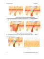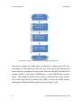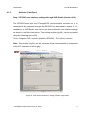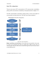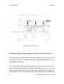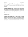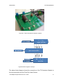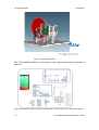
1
Technical Note PR-TN 2009/00597
Issued: 11/2009
Track-and-Flash for
Photoepilation Using Optical
Displacement Sensing
Dipen Parikh; B. Ackermann
Philips Research Europe
Unclassified
©
Koninklijke Philips Electronics N.V. 2009
PR-TN 2009/00597
Authors’ address
Unclassified
Dipen Parikh
[email protected]
B. Ackermann
[email protected]
© KONINKLIJKE PHILIPS ELECTRONICS NV 2009
All rights reserved. Reproduction or dissemination in whole or in part is prohibited
without the prior written consent of the copyright holder .
ii
©
Koninklijke Philips Electronics N.V. 2009
Unclassified
PR-TN 2009/00597
Title:
Track-and-Flash for Photoepilation Using Optical Displacement
Sensing
Author(s):
Dipen Parikh; B. Ackermann
Reviewer(s):
IPS Facilities
Technical
Note:
PR-TN 2009/00597
Additional
Numbers:
-
Subcategory:
-
Project:
Male Body Grooming (2008-041)
Photonic Therapy (2004-347)
Customer:
CL – Shaving & Beauty
Keywords:
photoepilation, Step-and-Flash, Track-and-Flash, displacement measurement, optical tracking, optical sensors, self-mixing interference, image processing
©
Koninklijke Philips Electronics N.V. 2009
iii
PR-TN 2009/00597
Unclassified
Abstract:
Light-based hair removal (photoepilation) has been applied by dermatologists and in beauty
parlours since more than a decade. A few photoepilation devices for at-home use have been
commercialized quite recently or will be available soon. For these it is a major challenge to
reduce the time needed for treating large areas of the body like the legs.
Operating these devices in Track-and-Flash mode instead of Step-and-Flash mode can
contribute significantly to achieving this goal. (In Track-and-Flash mode the device is tracked
across the skin and flashes are released automatically at equal intervals. In Step-and-Flash
mode the device is placed on the skin, a flash is released, and these steps are repeated on
adjacent spots on the skin.)
Whilst the Track-and-Flash concept is well known, hitherto no attempt has been made to
actually implement it. This report (master thesis of Dipen Parikh) describes the first steps
taken towards implementing the Track-and-Flash concept: A Philips Twin Eye Laser Sensor
measures the motion of a rotating disk and this information is used to trigger commercially
available flash lamp modules at equal intervals.
Conclusions:
The Philips Twin Eye Laser Sensor has been used successfully to realise a tracking system.
The functionality of the tracking system was tested and proven on the experimental setup and
also on different surfaces.
The Track-and-Flash concept has been successfully introduced on the experimental setup.
Flashes are being triggered on predefined safe conditions and at fixed intervals based on the
displacement being monitored by the sensor. Although from observations it can be stated that
flashes are being generated at equal distances travelled by the sensor, due to the limited energy generated by the flash modules available the overlapping of flashes could not be validated
with the means of a thermal camera.
iv
©
Koninklijke Philips Electronics N.V. 2009
Unclassified
©
Koninklijke Philips Electronics N.V. 2009
PR-TN 2009/00597
5
PR-TN 2009/00597
Unclassified
Contents Track-and-Flash for Photoepilation Using Optical Displacement Sensing ... i 1. Introduction .......................................................................................................................... 8 2. Hair Removal ...................................................................................................................... 10 2.1. Anatomy of Hair ......................................................................................................... 10 2.1.1. Melanin ......................................................................................................... 11 2.1.2. Hair Growth Cycle ........................................................................................ 13 2.2. Methods to Remove Hair........................................................................................... 14 2.2.1. Depilation ...................................................................................................... 14 2.2.2. Epilation ........................................................................................................ 14 3. Photoepilation .................................................................................................................... 16 3.1. Photochemical Damage ............................................................................................ 17 3.2. Photomechanical Damage ........................................................................................ 17 3.3. Photothermal Damage .............................................................................................. 17 3.3.1. Selective Photothermolysis .......................................................................... 18 3.4. Melanin and Light Interaction .................................................................................... 19 3.5. Light Sources............................................................................................................. 23 3.5.1. Light Sources for Hair Removal ................................................................... 26 3.6. Limitations and Side Effects of Photoepilation .......................................................... 29 4. Consumer Device Concepts ............................................................................................. 30 4.1. Point of Care and Home Applications, Usability, Safety ........................................... 30 4.2. Step-and-Flash .......................................................................................................... 33 4.2.1. Concept ........................................................................................................ 33 4.2.2. Discussion .................................................................................................... 35 4.3. Track-and-Flash ........................................................................................................ 36 4.3.1. Concept ........................................................................................................ 36 4.3.2. How to Implement the Track-and-Flash Concept ......................................... 36 5. Key Components for Track-and-Flash ............................................................................ 42 5.1. Displacement Sensor ................................................................................................ 42 5.1.1. Twin Eye Laser Sensor ................................................................................ 43 5.1.2. Serial Peripheral Interface (SPI) ................................................................... 47 5.2. Microcontroller ........................................................................................................... 55 5.2.1. STK500 Evaluation Board ............................................................................ 57 5.3. Test Bench ................................................................................................................ 58 6. 6
Implementation of Track-and-Flash ................................................................................. 60 ©
Koninklijke Philips Electronics N.V. 2009
Unclassified
PR-TN 2009/00597
6.1. Displacement Sensing (Implementation 1) ............................................................... 60 6.1.1. Hardware ...................................................................................................... 60 6.1.2. Software (TwinEye.c) ................................................................................... 71 6.1.3. Results .......................................................................................................... 85 6.2 6.3 6.4 7 Displacement Sensing in the Mechanical Setup (Implementation 2) ........................ 88 6.2.1 Hardware ...................................................................................................... 88 6.2.2 Software (TwinEye.c) ................................................................................... 90 6.2.3 Results .......................................................................................................... 90 Displacement Triggering Flashes (Implementation 3)............................................... 91 6.3.1 Hardware ...................................................................................................... 91 6.3.2 Software (TwinEye_Hamamastuflashmodule.c) .......................................... 95 6.3.3 Results .......................................................................................................... 97 Trigger Flash and Control Charging (Implementation 4) ........................................... 98 6.4.1 Hardware ...................................................................................................... 98 6.4.2 Software (TwinEye_TIflashmodule.c)......................................................... 102 6.4.3 Results ........................................................................................................ 104 Conclusions and Outlook ............................................................................................... 105 References ............................................................................................................................... 106 Figures...................................................................................................................................... 108 Tables ....................................................................................................................................... 110 Flow Charts .............................................................................................................................. 111 A C-Code .............................................................................................................................. 112 A.1 TwinEye.c ................................................................................................................ 112 A.2 TwinEye_Hamamatsuflashmodule.c ....................................................................... 114 A.3 TwinEye_TIflashmodule.c ....................................................................................... 116 ©
Koninklijke Philips Electronics N.V. 2009
7
PR-TN 2009/00597
1.
Unclassified
Introduction
Every individual, irrespective of gender and social status, strives to have perfect
looks and beautiful skin. Removal of unwanted hair has been an integral part of
the cosmetic field for a long time. Many methods have been developed for removal of unwanted hair: shaving, waxing, mechanical method (plucking) and
quite recently light-based hair removal.
Especially light-based hair removal depends on the anatomical features of hair
and the hair growth cycle. These are revieved and an overview of methods to
remove hair is given in chapter 2.
In the modern world, where time and comfort are of essence, light-based hair
removal (photoepilation) not only offers several distinct advantages over its less
sophisticated and sometimes painful mechanical counterparts, but also offers a
long term solution to the user. The working principle and some other aspects of
photoepilation are described in chapter 3.
Presently, these light-based technologies are used mainly in professional cosmetic instruments. These instruments are usually complicated to use, mostly
because their operation depends on various conditions and parameters such as
skin colour, energy intensity used in the treatment, duration of treatment, etc.
These instruments are only allowed to be operated by qualified individuals. In
contrast, consumer devices are made for dedicated use and are suitable for a
particular group of people. They have limited parameters to adjust. All existing
light-based hair removal devices are operated based on the Step-and-Flash
principle which is time consuming because the entire area of the skin under
treatment has to be covered with flashes which can be generated one at a time.
On the other hand the Track-and-Flash concept involves automatic generation
8
©
Koninklijke Philips Electronics N.V. 2009
Unclassified
PR-TN 2009/00597
of flashes at fixed displacement intervals during the treatment. Both Step-andFlash and Track-and-Flash techniques are discussed in chapter 4.
Chapter 5 deals with the technical requirements of the system, and based on
these requirements selection of the key components for implementing the
Track-and-Flash concept. This chapter deals also with the interfacing protocols
between the selected components and provides an overview of the mechanical
experimental setup.
The hardware and software of four different implementations used to validate
the Track-and-Flash concept are explained in detail in chapter 6 and results
obtained are discussed.
©
Koninklijke Philips Electronics N.V. 2009
9
PR-TN 2009/00597
2.
Hair Removal
2.1.
Anatomy of Hair
Unclassified
We have two types of hair on our body: the vellus hair and the terminal hair.
Vellus hair is soft, fine and short. It is nearly unnoticeable but in some men or
women it can be darker and noticeable. This hair helps the body to maintain
the body temperature by providing insulation. The terminal hair grows on the
head, the armpits and the pubic region. It is coarse, longer and darker than the
vellus hair. Men have terminal hair on chest and back. Terminal hair is for protection and acts as anti-friction layer between two skin surfaces or skin and any
other surface e.g. a moving arm rubbing against the body [1] [2].
The hair can be divided into two parts, the root and the shaft. The hair part
outside of the skin is called shaft. The root part of the hair is in the skin (dermis)
as shown in fig.1. A pouch like structure called follicle surrounds the hair root.
The base of the hair root is in the shape of a bulb. The centre of the bulb is
Figure 1 Anatomy of hair [24]
10
©
Koninklijke Philips Electronics N.V. 2009
Unclassified
PR-TN 2009/00597
called papilla. The papilla is surrounded by the matrix. The papilla is fed by very
small blood vessels, which bring food and oxygen to it and take wastes away.
The papilla is highly sensitive to hormones. New hair material is formed out of
specialized skin cells of the hair matrix. The cells in the matrix divide. The newly
divided hair cells push the previous cells up. The cells, which move upwards,
die slowly forming the hard hair shaft. The sebaceous glands shown in fig.1 are
usually attached to the hair follicles and secrete an oily matter (sebum) in the
hair follicles to lubricate the skin and the hair [1][2].
2.1.1.
Melanin
The colour of our hair and the skin are determined by pigments produced in
cells, which are called melanocytes. Melanocytes produce a chemical pigment
called melanin. This chemical compound that reflects certain wavelengths of
visible light determines the colour of the hair and the skin. Fig.2 shows a microscopic view of the melanocytes in the skin, which are responsible for the skin
colour. These melanocytes are present only in the epidermis layer of the skin.
The skin layer below the epidermis is called dermis. It has no melanocytes cells
except in the hair in the matrix close to the dermal papilla which is responsible
for the hair colour [1][2].
Figure 2 Pigmented cells in skin [26]
©
Koninklijke Philips Electronics N.V. 2009
11
PR-TN 2009/00597
Unclassified
The melanin produced in the matrix is also present in the hair shaft. There are
two main pigments found in the human hair: Eumelanin
and Pheomelanin.
Eumelanin has an oval or an elliptical shape. It gives colour to brown or black
hair and is the dark pigment. A higher concentration of Eumelanin causes
darker hair. Pheomelanin produces the colour in blonde or red hair. The higher
the concentration of Pheomelanin, the lighter the hair. Unlike Eumelanin,
Pheomelanin is smaller, partly oval and has a rod shape. White hair contains no
melanin at all and gray hair contains only a few melanin granules. The amount
and density of the melanin in the shaft determines the exact colour of the hair.
The colour, shape and thickness are determined by genetics [1] [2].
There are also cells in the hair follicle which are not pigmented called stem
cells (no melanin in these cells) shown in fig.3. These cells lie at the outer root
area called bulge near the attachment of the arrector pili muscle, some distance
from the pigmented area. These cells are essential for the hair growth cycle
[27].
Figure 3 Stem cells [27]
12
©
Koninklijke Philips Electronics N.V. 2009
Unclassified
2.1.2.
PR-TN 2009/00597
Hair Growth Cycle
Traditionally, there are mainly three phases of the hair growth cycle recognized:
Anagen phase: It is an actively growing phase. The papilla is connected with
the blood vessels. Cells in the matrix are divided and grow upward to form the
hair shaft. Depending on the location this phase may last for several years [2].
Catagen phase: Once a hair reaches its full length, cell division and pigmentation stops. The hair becomes fully keratinised with a swollen “club” end and
moves up towards the outer layer of the skin and rests there. This phase is
called the catagen phase [2].
Telogen phase: After a short rest period, the dermal papilla cells and keratinocyte stem cells become active again and a new hair grows from the new follicle.
The old hair gradually gets lost from the surface. This phase is called the telogen phase [2].
Recent research suggests that shedding of the hair fibre is an active process
and introduce the new term exogen for this phase. After shedding of the hair
fibre, the hair follicle remains empty. This phase has been named kenogen [2].
Figure 4 Hair growth cycle [25]
©
Koninklijke Philips Electronics N.V. 2009
13
PR-TN 2009/00597
Unclassified
Fig.4 represents the hair growth cycle starting with the anagen phase which is
the growing phase to the telogen phase which is the end of the old hair and
starting of the new hair [2].
2.2.
Methods to Remove Hair
Hair styles or preference for hairless skin are influenced by the culture, society
or from the entertainment world. From ancient time to now different methods
have been used to remove unwanted hair from the body. As technology developed, more advanced and sophisticated methods and related devices became
available. Each method has its own advantages and drawbacks. Parameters to
be considered for the different methods are the time needed for the treatment,
its efficiency in terms of whether hair removal is temporary or permanent and
side effects like skin irritation.
Hair removal methods can be categorised in terms of removing hair from above
the skin or below the skin.
2.2.1.
Depilation
Depilation removes only that part of the hair that is outside of the skin surface.
Since the depilation method removes only part of the hair, one has to repeat it
frequently [1].
Shaving is the most common example of depilation. With a sharp blade it cuts
the
hair just above the uppermost skin layer.
Chemical Cream applied to the skin dissolves the hair.
2.2.2.
Epilation
Epilation removes also (part of) the hair below the skin surface. It can further be
categorised as temporary or permanent [1].
14
©
Koninklijke Philips Electronics N.V. 2009
Unclassified
PR-TN 2009/00597
Electrolysis is the method in which a fine needle is inserted into the skin. A
small current is applied to the hair follicle root which is burned out. Each hair
follicle must be treated individually and it may take several treatments to destroy
the follicle. It is a permanent hair removal method in most patients [4].
Plucking is a temporary method, a person stretches the skin and pulls out the
hair using tweezers. It is painful and time consuming because one can work on
one hair at a time [4].
Waxing is similar to plucking, the only difference is that it removes many hairs
at a time. A wax is applied to the skin surface. A cloth strip is then applied over
the wax and quickly pulled off. It is painful but less time consuming.
Epilator is a temporary hair removing method which removes the hair using a
mechanical device. Instead of pulling a single hair using tweezers as in the
plucking method, an electrically rotating roller is used which pulls out many
hairs simultaneously but not as many as waxing does. It is a painful method
because multiple hairs are pulled out at a time from deep into the skin.
Photoepilation is the method of removing hair using a light source. Light penetrates into the skin. Light energy is absorbed by melanin present in the hair
follicle which generates heat which damages the hair follicle. It is not removing
hair at the time of treatment but disturbing the hair cycle or destroying the hair
follicle. Lasers and IPL (Intense Pulse Light) are used as light sources [2]. Removing hair using photoepilation is temporary or permanent, depending on its
fluence rate. If the fluence rate is less than 10 J/cm² then it removes the hair
temporary but if the fluence rate is greater than 20 J/cm² then it damages the
hair follicle strongly and results in long term hair removal [28].
©
Koninklijke Philips Electronics N.V. 2009
15
PR-TN 2009/00597
3.
Unclassified
Photoepilation
Light has been used widely and effectively in medical science and cosmetics. It
is playing an important role for diagnosis and treatment. Different parts of the
spectrum interact in different ways with the body because they have different
energies and that way different interactions with the human body are created.
Examples for the applications of light for medical purposes are the infrared light
used for pulse oximetry,
thermograpy and near infrared spectroscopy. Visible
light is used for endoscopy, ophthalmoscopy and photodynamic therapy. Blue
light is used for the treatment of jaundice. X-rays are used for radiotherapy.
Light is also used for a range of cosmetic treatments like for removal of unwanted hair, skin rejuvenation, wrinkles, cellulite reduction and acne treatment.
The concept of hair removal using light is based upon the principle of selective
photothermolysis [2]. It damages hair follicles in such a way that it slows down
or stops re-growth. It has shown effective and long term results. This damage
can happen because of the absorption of light in melanin. Melanin is a natural
chromophore in the hair follicle which absorbs light and radiates heat into the
surrounding area. Other chromophores in the skin i.e. hemaglobine, oxyhaemaglobin and water also absorb light. Hair removal using light sources is
getting increasingly popular. Lasers with different wavelengths and IPL (Intense
Pulse Light) are used for hair removal [2]. It is effective but knowledge about
appropriate treatment is necessary since otherwise it can cause side effects.
There are three mechanisms by which light can damage hair follicles [2].
Photochemical damage
Photomechanical damage
Photothermal damage
16
©
Koninklijke Philips Electronics N.V. 2009
Unclassified
3.1.
PR-TN 2009/00597
Photochemical Damage
Photochemical interaction of light with tissue is of great interest for cosmetic
treatments like skin aging process, tissue repairing, rejuvenation, hair removal
treatment. Photochemical damage is the use of light to produce a targeted
photochemical reaction and therapeutic effect. This chemical reaction damages
cell membranes and the protein. This reaction and effect depends on the type of
the targeted chromophore [1].
3.2.
Photomechanical Damage
When light travels into the skin, it is getting absorbed and generates heat. This
heat increases the temperature of the tissue and results in reversible or irreversible alterations in the tissue. Multiple short pulses cause extremely rapid
heating of the target. A temperature greater than 100°C is causing photomechanical destruction of tissue. Due to the high temperature, pressure is generated in the tissue which can stimulate shock wave formation and mechanical
damage of the tissue [1]. Photomechanical destruction of hair has been attempted with very short nanosecond pulses by Q-switched 1064-nm Nd:YAG
lasers, both with or without carbon suspension as an additional chromophore
[2]. Hair follicles targeted with very short pulses cause extremely rapid heating
of the chromophore. This generates photo acoustic shock wave which leads to
photomechanical destruction.
3.3.
Photothermal Damage
Photothermal damage is related to the method of use of light as used in photomechanical damage, the major difference is that instead of shockwave generation this works by thermal transfer. In photothermal damage, the tissue temperature does not rise above 100°C [1]. Photothermal damage is based on the
principal of selective photothermolysis [2].
We consider devices using the
photothermal damage method.
©
Koninklijke Philips Electronics N.V. 2009
17
PR-TN 2009/00597
3.3.1.
Unclassified
Selective Photothermolysis
The principle of selective photothermolysis comprises that “by choosing appropriate wavelength, pulse duration and fluence, thermal injury can be confined to
a target chromophore” [2]. Selective photothermolysis provides a thermal damage to the target with minimum disturbance of the surrounding tissue.
Wavelength: The wavelength of the electromagnetic radiation has to be selected to provide maximum contrast of absorption of the target vs. the surrounding tissue and other competitive targets [1].
In the human body natural chromophores are present. The most important
chromophores in the skin are melanin, haemoglobin and water.
Melanin is
present in the epidermis layer of the skin, in the hair root and in the hair shaft.
Haemoglobin and water are distributed in all the tissue mostly at every layer.
These chromophores have different bands of absorption as shown in fig.5.
Figure 5 Relative absorption of melanin, blood and water [24]
18
©
Koninklijke Philips Electronics N.V. 2009
Unclassified
PR-TN 2009/00597
Oxyhaemoglobin absorbs light mainly at shorter wavelengths between 300nm
and 650nm with peak absorption between 400nm to 450nm. Water absorbs
light mainly at longer wavelengths above about 1000nm with peak absorption
around 2000nm. Melanin has a decreasing graph of absorption. It absorbs more
light at shorter wavelength and absorption is decreasing as the wavelength is
getting longer. An interesting property of melanin is that starting around 600nm
to 1200nm, melanin has higher absorbing region than other chromophores i.e.
water and haemoglobin. In this region of its absorption band, melanin becomes
a useful tool for cosmetic applications [1].
Pulse duration: The pulse width of the electromagnetic radiation has to provide
maximum contrast of heating of the target versus surrounding tissue [1]. The
pulse duration is related to the generation of heat in the tissue. Long pulse
duration transfers more energy into the tissue than short pulses. Because of the
greater amount of energy, long pulse duration generates more heat into the
tissue. The pulse duration that confines most of the heat generated to the target
tissue is called thermal relaxation time. The thermal relaxation time for hair
removal is estimated to be between 10ms to 100ms. Pulse duration greater
than the thermal relaxation time is called thermal damage time (TDM). Pulse
duration with thermal damage time damages also tissue surrounding the targeted tissue [1].
Fluence rate: The fluence rate is the amount of energy striking on the targeted
area at a time resulting in the generation of heat. Fluence of the pulse has to be
sufficient to provide the desired effect [1].
3.4.
Melanin and Light Interaction
The interaction of light with the skin is a complicated process. Skin is a tissue
that has reflecting, scattering and absorbing optical properties. It has a higher
reflective index than the air which causes partial reflection of the light when
hitting the skin surface, while the remaining part penetrates into the skin. Light
propagation within the skin depends on the scattering and the absorbing proper©
Koninklijke Philips Electronics N.V. 2009
19
PR-TN 2009/00597
Unclassified
ties of the various compartments like cells, organelles etc. Multiple scattering
and absorption decreases the intensity of the light propagating deep into the
skin. This absorption transforms light energy into other forms of energy, mostly
heat. A chromophore is a molecule which absorbs light. There are many kinds
of chromophores in the human body e.g. haemoglobin, bilirubin, carotenoids,
porphyrins and melanin. These chromophores have particular absorbing bands
in the electromagnetic spectrum where they react while interacting with the light
[1].
Melanin in the hair causes the colour of hair like melanin in the epidermis layer
of the skin causes the colour of the skin. For the hair removing concept using
the selective photothermolysis principle, melanin in the hair follicle is the main
target. This can be done by targeting the absorbing region of melanin and
avoiding the absorbing regions of other chromophores. Damaging the target
tissue with or without disturbing surrounding tissue depends on the pulse duration. Temporary or permanent removal of hair depends on the fluence rate [1]
[2].
Selection of wavelength
Melanin is a natural chromophore present in the hair shaft and the hair matrix.
As shown in fig.5, melanin has a wide waveband of absorption from visible light
to the near-infrared region. Major competitor chromophores to the hair melanin
are blood, water and epidermal melanin. Using the absorption spectrum shown
in fig.5 one can estimate the optimum absorption band of the targeted hair
melanin taking into account competitive chromophore absorption bands. Additional parameters taken into consideration while selecting the wavelength is the
location of the targeted melanin with respect to competitive targets and the
concentration of the melanin [1][2].
Melanin in the hair lies between 2 mm to 5 mm depth in the skin [3]. So the
penetration length of light source for targeting hair melanin should be selected
between these depths. Deep, selective heating of the hair shaft and the heavily
20
©
Koninklijke Philips Electronics N.V. 2009
Unclassified
PR-TN 2009/00597
pigmented matrix are possible in the region of 600-1100nm [2]. Most lasers
successfully utilised for hair removal emit radiation with wavelengths avoiding
the major absorption peaks of haemoglobin and water. As shown in fig.5 the
ruby laser can be most suitable for hair removing concept because it has a
wavelength of a 694nm where the absorption of haemoglobin and water are
low. However other lasers have also shown effective results e.g. alexandrite
laser, diode laser and Nd:YAG laser. Lasers generate a single wavelength
whereas an Intense Pulsed Light source generates a complete spectrum of
light. Using appropriate filter wavelengths between 600nm to 1200nm can be
filtered out from the flash lamp spectrum and can be used for the whole absorbing region of the melanin [1][2].
Not all of the light is absorbed by the hair melanin, some energy is absorbed by
the skin melanin also which may result in burning effect on the skin. Dark skin
has a high amount of melanin in the epidermis layer of the skin which gives
highest burning effect. The photoepilation method is facing a conflict between
these two melanines. Some cooling methods like cold air flow, gel, ice can
minimize thermal injury of the epidermis layer [2].
Selection of pulse duration
Thermal transfer theory suggests that pulse duration of light targeted to melanin
also plays an important role. The follicular structures will get heated because of
the thermal conduction from the melanin-rich shaft and matrix. Long pulse duration will generate more heat which also damages the surrounding tissue. For
damaging of just the hair follicle, the pulse duration should be shorter or equal
to the thermal relaxation time of the hair follicle. For permanent hair destruction
another type of cells is playing an important role which are called the follicular
stem cells (discussed before in chapter 2.1. Anatomy of Hair). To damage these
stem cells the pulse duration should be greater than the thermal relaxation time
i.e. in the region of thermal damage times. The light absorbed by the melanin
present in the hair root, generates also heat. This heat will propagate through
the entire volume of the hair to better damage the stem cells [2].
©
Koninklijke Philips Electronics N.V. 2009
21
PR-TN 2009/00597
Unclassified
Selection of Fluence
Fluence is playing an important role for long term hair removal. As discussed
previously (in chapter 2.1. Anatomy of Hair), a fluence less than 10J/cm² cannot
create enough heat to damage the hair follicle strongly. Fluences above 20
J/cm² damage the hair follicle strongly resulting in permanent hair loss. Careful
studies with computerized hair counts have demonstrated that greater hair loss
is achieved at the higher fluences tested [2]. However, the skin type and the
colour of the hair are major factors in determining a suitable fluence. A higher
fluence will give more burning effect on the skin surface. Dark black skin has a
large amount of melanin present in the skin. This will give more burning effect
on the skin surface than with the fair skin.
22
©
Koninklijke Philips Electronics N.V. 2009
Unclassified
3.5.
PR-TN 2009/00597
Light Sources
Light is electromagnetic radiation in the UV, visible and NIR region of the electromagnetic spectrum. Visible light ranges between 400nm to 800nm starting
from violet to the red. Light that is more violet than violet called ultraviolet light
(UV) ranges from 10nm to 400nm and light redder than red is called infrared
light (IR) in the range between 800nm to 3000nm [23].
Figure 6 Visible light spectrum [23]
Generation of light can be natural or men made. Light sources can be categorised as incandescent, gas discharge and solid state. An incandescent
source is an object heated so much that it gives off light. It can be described
theoretically as a black body which emits different radiation as its temperature
increases. A gas discharge source uses electrodes and gas to generate light.
Intensity and colour of the light emitted by the source depend on the type of gas
used and the pressure of the gas in the tube. A solid state source is built entirely from solid materials and generates light electronically. These solid materials are semiconductors, and the colour of the light emitted from solid state depends on the type of semiconductor used.
©
Koninklijke Philips Electronics N.V. 2009
23
PR-TN 2009/00597
Unclassified
Incandescent means giving off light as a result of being heated. The sun is a
natural source of incandescent light. The sun emits light because of a very slow
reaction in which hydrogen burns to helium. Man made incandescent light
sources are candles, incandescent light bulbs etc. Candles consist of fuel material mostly wax or fat. When it comes into contact with fire, using oxygen, a
reaction starts and gives output in form of visible light and carbon vapour. In an
incandescent light bulb, the electricity goes through the connecting wires into
the bulb. The electricity then gets forced to go through a very tiny and thin wire
called the filament. The electrons have a tiny amount of space to go through, so
the filament heats up. The filament then gets heated up until it finally glows.
Incandescent light bulbs are not very efficient, because a large portion of the
electricity is converted to heat instead of useful light. It also takes a long time to
get heated up.
A gas discharge tube uses a low-pressure gas or high pressure gas to create
light. Gases used are mercury, neon, argon, xenon and krypton. A gas discharge tube with low pressure has no electrode inside. Light is generated by an
electrical discharge, the gas gets ionized and forms a plasma. A high pressure
filled gas discharge tube called arc lamp has electrodes inside. The gas between two electrodes between which a high potential difference exists, gets
ionized and forms a plasma. The free electrons in this plasma allow current to
flow between the electrodes. The plasma either generates light directly, or by
causing another material to create light. The mercury lamp and Intense Pulsed
Light (xenon flash lamp) are the most common examples of gas discharge
lamps.
Solid state light sources are light emitting diodes (LEDs), organic LEDs
(OLEDs) and diodes lasers etc. LEDs are basically semiconductor material
diodes. When the diode comes into forward bias electrons and holes are recombined and generate light. The colour of the light depends on the energy gap
of the semiconductor. OLEDs are composed of organic material and emit light
similar to LEDs. In a laser radiation of light occurs through a stimulation proc24
©
Koninklijke Philips Electronics N.V. 2009
Unclassified
PR-TN 2009/00597
ess. The wavelength of the light generated by the laser depends on the active
medium used such as gas, solid state, liquid and semiconductor (diode) lasers
[1].
For medical use, lasers and IPL (xenon flash lamp) are used in many applications.
Lasers are devices that generate a beam of light that is collimated, monochromatic and coherent. The radiation of a laser can be characterized by its wavelength, power, and the mode of light generation either continuous mode or pulse
mode. A continuous mode laser can work in pulse mode but most pulse mode
lasers cannot work in continuous mode. The lasing material used can be a gas,
liquid or a solid [1].
From the gas lasers in which a gas is used as the lasing medium, the carbon
dioxide laser is mostly used in medical application for tissue ablation because of
the high absorption by tissues. It can generate wavelengths in the infrared
range from 9.2 to 11.1 µm. These lasers are tuneable within this range [1].
From the liquid lasers in which a liquid is used as the lasing medium, the dye
laser is used in spectroscopy, photochemistry of biological molecules and for
blood vessels coagulation. It can emit wavelengths from 340-960nm, 217380nm and 1060-3100nm [1].
A solid state laser has as its active medium a matrix of crystal, glass or ceramic
doped by active ions. As crystal matrices sapphire, yttrium aluminium garnet(YAG), alexandrite and other materials are used in lasers. Active ions can
be Nd(neodymium), Cr(chromium), Er(erbium), Ho(holmium), Tm(thulium) and
others [1]. Active ions generate different wavelengths depending on the matrices used. The combination of Nd:YAG is the one of the most efficient laser in
photomedicine which generates light in the near infrared region e.g. 1064nm.
The Er:YAG combination generates wavelengths in the mid-infrared region i.e.
©
Koninklijke Philips Electronics N.V. 2009
25
PR-TN 2009/00597
Unclassified
2.79-2.94µm. It is used in tissue ablation [1]. From the diode lasers one of the
most used lasers is the GaAs laser using gallium arsenide (GaAs) as a semiconductor material. It emits in the near infrared range (NIR) at about 830nm. It
can produce many wavelengths depending on the semiconductor material used
[1].
An Intense Pulsed Light source (IPL) is a xenon flash lamp that uses light emission of a plasma bridge formed in a gap between two conductors [1]. Intense
Pulse Light Sources (IPL) is used in spectroscopy and dermatology. They are
filled with xenon and krypton gas known as xenon lamp or krypton lamp respectively. They are emitting the entire wavelength of visible light (including UV and
IR) present in the electromagnetic spectrum.
3.5.1.
Light Sources for Hair Removal
For hair removal we need a light source which has a controlled flash, operates
in pulse mode and should not generate much heat while producing light. Controlled flash means that it can be flashed within millisecond just after triggering.
In pulse mode, the duration of a pulse can be controlled and as described previously (selective photothermolysis principle), the pulse duration plays an important role for the hair removing concept. The generation of extensive heat with
light will create a burning effect on the outer layer of the skin which has to be
avoided for the removal of hair.
An incandescent lamp generates a significant amount of heat while generating
light. It needs start up time and shut down time. It first gets heated up and then
radiates light. So it is hard to control the radiation of light. It cannot be operated
in pulse mode which is very important for hair removal application. Because of
this incandescent light sources are not used for hair removing application. Gas
discharge lamps have the advantage that they can radiate all wavelengths of
visible light, UV and IR. They convert major energy into light instead of heat and
they can be operated in pulse mode. This is suitable for hair removing application. Solid state light sources, LEDs cannot generate enough intensity needed
26
©
Koninklijke Philips Electronics N.V. 2009
Unclassified
PR-TN 2009/00597
for hair removal application but lasers can be used for hair removal application.
Lasers generate parallel light which has a focused beam and which can also be
generated in pulse form. Laser produces a single wavelength. Lasers with
wavelength between 600nm to 1100nm are suitable for hair removal application.
The major light sources (Lasers and IPL) used for hair removal are shown in the
Table (1). Skin type Table (2), hair colour and hair diameter are mainly taken
into consideration for the selection of the light source.
According to Table 2. The Q-switched Nd:YAG and the Intense Pulsed Light
source are suitable for all skin types and dark to light brown hair colour. Ruby,
Alexandrite, pulsed diode, Nd:YAG lasers and intense pulsed light sources can
provide hair removal.
We consider Intense Pulsed Light sources for hair removing device. All light
sources suited for photoepilation emit a single wavelength except Intense
Pulsed Light source which is producing visible light, UV and IR wavelength of
electromagnetic spectrum. It is an advantage of Intense Pulsed Light sources
that using filters they can cover the optimum absorption band of the hair melanin.
Table 1 Indications and expected efficacy for different hair-removal devices [2]
Laser or Light source
Skin
type
Hair colour
Hair diameter
Expected efficacy
(Table 2)
Normal-mode Ruby
I-III
Dark to light brown
Fine and Coarse
Long-term hair removal
Normal-mode Alexandrite
I-IV
Dark to light brown
Fine and coarse
Long-term hair removal
Pulsed diode
I-V
Dark to light brown
Coarse
Long-term Hair removal
Normal-mode Nd:YAG
I-VI
Dark
Coarse
Long-term hair removal
Q-switched Nd:YAG
I-VI
Dark to light brown
Fine and Coarse
Temporary hair removal
Intense pulse light
I-VI
Dark to light brown
Coarse
Long-term hair removal
©
Koninklijke Philips Electronics N.V. 2009
27
PR-TN 2009/00597
Unclassified
Table 2 Skin type and colour [2]
Skin Type
Colour
I
very light
II
light
III
light intermediate
IV
dark intermediate
V
dark (Brown)
VI
very dark (Black)
Intense Pulsed Light sources are non-coherent, multi-wavelength light sources.
By using appropriate filters, the wavelength range from 600-1200nm can be
emitted. As mentioned in fig.5 (Graph of absorption of melanin) melanin has a
wide range of absorption and in the range between 600 to 1200nm there is no
major peak absorption of any other chromophore. So using an intense pulsed
light source deeply penetrating wavelengths which are most suitable for melanin
of the hair can be obtained. It can be used with single or multiple pulses with
different durations and delay intervals. The wide choice of wavelengths, pulse
durations and delay intervals makes IPL devices potentially effective for a wide
range of skin types [2].
28
©
Koninklijke Philips Electronics N.V. 2009
Unclassified
3.6.
PR-TN 2009/00597
Limitations and Side Effects of Photoepilation
Laser hair removal was FDA cleared in 1996 and has an excellent safety and
efficacy profile. Complications are rare if treatments are done carefully and with
the patient’s skin type in mind [2].
Limitations:
(1) Multiple treatment sessions are required to achieve the maximal level of
hair reduction.
(2) Some patients with light skin colour and finer hair can have re-growth of
hair.
(3) It is not suitable for patient with skin disease.
Side Effects:
Some temporary or permanent side effects can occur using any light source
based hair removal treatment.
(1) Laser hair removal is not a painless procedure. This depends on the fluence rate and skin type.
(2) Epidermal damage occurs if excessive fluencies are used.
(3) The most common side-effects are transient pigmentary changes such as
hypopigmentation or hyperpigmentation. It can be prevented if the appropriate treatment fluencies are chosen for a certain skin type.
(4) Retinal injury can happen if proper eye protection is not provided.
©
Koninklijke Philips Electronics N.V. 2009
29
PR-TN 2009/00597
Unclassified
4.
Consumer Device Concepts
4.1.
Point of Care and Home Applications, Usability, Safety
Nowadays, medical and cosmetic consumer devices are becoming part of the
daily life of people. New technologies aim at satisfying requirements with respect to comfort and safety. These technologies make use of scientific results
obtained with and research aiming at professional systems. The challenge is to
develop small, affordable devices that are powerful enough to be effective, but
safe enough to be used by consumers [5].
Skin care and hair care products attract a lot of attention both by people and by
companies. Many people spend countless hours per week in the shower, shaving and cutting themselves in a relentless pursuit of hairless skin that is smooth
to touch or spend series of sessions at clinics or spas to treat a particular area
of the skin even though it costs huge professional fees [5].
Professional cosmetic instruments are usually complicated to use, mostly because they are designed to operate in various conditions with selection of various parameters. They are only allowed to be operated by qualified persons.
Before the treatment the treatment area is examined and then possible benefits
and the side effects are considered. These treatments last over longer periods.
Various sessions are necessary to obtain the expected result. This is not affordable in terms of cost and time for all people. In contrast, home use devices
are made for dedicated use and suitable for a particular range of people. They
have limited parameters to adjust. One can do the treatment as described in the
user manual on a convenient time. Treatment effects, safety features, warnings
and side effects are described in the user manual. It is only one time cost expenditure, except that some accessories may need to be changed.
Since recently several companies are releasing light based hair removing consumer devices that offer many of the advantages of professional treatment and
30
©
Koninklijke Philips Electronics N.V. 2009
Unclassified
PR-TN 2009/00597
put them right within customers’ hands at their own home. Home hair removing
devices are expected to become increasingly popular in the near future. The
key benefits are privacy, convenience, affordability and no committed appointments at a clinic. TriaBeauty [7], Silk’n [8], Philips SatinLux [9] are some examples of the devices that are in the market.
Hence innovative devices provide individuals with the ability to remove unwanted hair safely and effectively in the comfort of their own home, while this
method can save users plenty of time and money.
Philips SatinLux fig.7 is one of the at-home hair removing devices. The procedure is non-invasive, requiring no needles or chemical applications. Compared
to electrolysis, large areas of skin can be treated in a shorter period of time.
This device removes hair using the IPL technology. (The IPL technology is
discussed in chapter 3.5 Light Sources.)
4
1
5
6
3
2
Figure 7 Philips SatinLux photoepilation device [22]
Fig.7 shows the key parts of the SatinLux device, No.(1) is the device on/off
switch, No.(2) is the light exit window with a filter glass in it. No.(3) is the safety
©
Koninklijke Philips Electronics N.V. 2009
31
PR-TN 2009/00597
Unclassified
system, comprising several contact switches. Only when all of these switches
are fully pressed then a flash can be released. No.(4) is the safety indication, a
light indicates when the safety switches are pressed and the device is ready to
flash. No.(5) is the button for adjusting the flash intensity from level 1 to 5. The
required intensity level depends on the skin and the hair type. No.(6) is the flash
trigger button. Use of this device is easy. The user has to adjust the intensity
level of the light according to the skin and the hair type as described in the
manual. The operation of this device uses a concept called Step-and-Flash.
Figure 8 Block diagram of SatinLux device
Fig.8. shows a block diagram of the SatinLux device. The flash is operated by
the user through the control unit. User inputs represent the trigger button and
the flash intensity adjust button. User feedback is representing the status of the
safety system and the intensity level. All modules are connected to internal
control unit.
32
©
Koninklijke Philips Electronics N.V. 2009
Unclassified
4.2.
Step-and-Flash
4.2.1.
Concept
PR-TN 2009/00597
The device’s light emitting surface is pressed on the skin and then a flash is
triggered. Then the device is moved to an adjacent part of the skin area. The
light emitting surface is pressed on the skin again and then a flash is triggered
again. This procedure is repeated step by step until the entire body part with
unwanted hair is covered with flashes. This procedure is called Step-and-Flash.
The SatinLux device has a fixed size of the light emitting window (3cmx1cm), so
at a time it can cover 3cm² areas on the body. Fig.9 shows the Step-and-Flash
concept and how it targets the hair follicles.
Figure 9 Step-and-Flash
As shown in fig.9, step 1 is to press the light emitting surface on the targeted
skin area and trigger the flash. Light penetrates into the skin. Fig.10 shows a
detailed view of the hair follicle before the flash and just after triggering the
flash.
©
Koninklijke Philips Electronics N.V. 2009
33
PR-TN 2009/00597
Unclassified
Figure 10 Hair in skin, before flash and just after flash [21]
The light selectively targets the melanin in the hair fig.11, The melanin absorbs
the light and generates heat elevating the temperature of the hair follicle.
Figure 11 Melanin in hair, heated hair bulb [21]
As a consequence of this the hair goes into resting phase, fig.12. A natural
process sheds the hair.
Figure 12 Damaged hair, area without hair [21]
34
©
Koninklijke Philips Electronics N.V. 2009
Unclassified
PR-TN 2009/00597
Now back to fig. 9, after step 1 the device is lifted up and moved to an adjacent
area shown as step 2. There is some area in between where subsequent
flashes overlap and there may be an area where there is no light penetrating
into the skin. Overlap between two adjacent steps is necessary because there
is less intensity at the border area. Hair follicles in the area left out between two
steps will remain unaffected. To avoid that the user must stay concentrated
during the treatment.
Optimal results cannot be obtained with a single session, The anagen phase of
the hair growth cycle is the only phase for the effective treatment, but during
treatment, hairs in the treatment area are usually in different stages of the cycle
of hair growth. To treat all hairs successfully one has to repeat this treatment.
Clinical trials have shown that repetition of treatment every 2 weeks gives optimal results.
4.2.2.
Discussion
In the following some characteristics of SatinLux with Step-and-Flash concept
are discussed that indicate potential areas for product improvements.
Number of flashes and treatment time: One of the flashes can cover 3cm²
area of the body. As stated in the manual it takes 25 flashes per armpit and it
takes approximately 3 minutes of treatment time. The entire bikini area needs
approximately 90 flashes and takes 10 minutes. This time is appropriate for a
small area and it will not be difficult for the user to spend 10 minutes time every
two weeks. But as to larger areas like one full leg it needs 320-380 flashes and
approximately 30 minutes of treatment time. This points to an opportunity for
improving system performance to reduce the time of treatment on larger body
areas.
Keep track on steps: Light penetrates into the skin in the shape of a cone.
There is less intensity of light at the border part which is not sufficient to gener©
Koninklijke Philips Electronics N.V. 2009
35
PR-TN 2009/00597
Unclassified
ate enough heat for hair follicles (see fig.9). If no overlap at the border area is
achieved then in the area left out in between hair follicles are unaffected. For
larger body parts it may be difficult to keep track on each step. User support
may be desirable.
Power for flashes: SatinLux works using rechargeable batteries, these batteries must be charged before using the device. As mentioned earlier a single leg
needs 320-380 flashes and approximately 30 minutes of time. A fully charged
battery offers 160 flashes at maximum intensity level (level 5) which means
approximately 15 minutes. Improved power handling is desirable.
The above points indicate opportunities for a new concept for a faster and more
sophisticated device, which should keep track on treatment, consume less time
and give the user feedback in a more sophisticated way. Such a Track-andFlash concept is described in the following.
4.3.
Track-and-Flash
4.3.1.
Concept
“The device is tracked across the skin and at fixed intervals of displacement
flashes are released automatically without lifting the device”. This concept has
the vision to make a device which works like shaving razor which removes hair
but here it stops hair growth for a longer time, without any shaving cream or
chemical. The principle behind the temporary hair removal is exactly the same
as in SatinLux. The difference is that this device will be more sophisticated, less
time consuming to use.
4.3.2.
How to Implement the Track-and-Flash Concept
The Track-and-Flash concept implies a device comprising a tracking module
and a flash module. Both communicate with each other in order to perform
flashes at predefined intervals, guide the treatment speed in a way to give optimum results of treatment, and make the treatment fast and safe for at-home
use.
36
©
Koninklijke Philips Electronics N.V. 2009
Unclassified
PR-TN 2009/00597
Figure 13 Track-and-Flash concept
Fig.13 shows the Track-and-Flash concept. Compared to Step-and-Flash
shown in fig.9, where flashes are released in a sequence of steps, here the
device is tracked across the skin. Flashes are released in a continuous manner
within predefined intervals of distance and overlap at the border area.
Figure 14 Track-and-Flash device concept
©
Koninklijke Philips Electronics N.V. 2009
37
PR-TN 2009/00597
Unclassified
Fig.14 represents the block diagram of a device that would implement the
Track-and-Flash concept.
Compared to the SatinLux device block diagram
shown in fig.8 one module is added that is “Displacement Sensing”. This is a
key module of the Track-and-Flash concept. This module affects the device’s
safety module, feedback module and the functionality of the flash. All together it
increases the complexity of the control.
The Displacement Sensing module is introduced to measure displacement of
the device while moving on the skin. Displacement Sensing can be done by
I)
Mechanical technology
II)
Optical image processing technology
III)
Laser self mixing technology
Mechanical technology can sense movements using moving parts. Tracking
can be achieved in many ways for example using a computer mouse with a
roller ball. The mechanism with roller ball rotates x and y axis gears in x and y
direction respectively and gives displacement with reference to a previous
place.
This simple roller ball mechanism can be selected as Displacement
Sensing module on the skin which gradually moves along on the skin and attach to it an encoder used in motors for counting the number of rotations. This
way one can give user feedback in terms of distance or area treated until now.
In principle mechanical way of tracking should work but this would make the
Figure 15 Mechanical technology
38
©
Koninklijke Philips Electronics N.V. 2009
Unclassified
PR-TN 2009/00597
device bulky and may be less accurate. In the case of a roller ball used as a
tracking device, the roller ball needs some projected area which comes in surface contact and in that way the roller ball moves across the surface. A mechanical or optical device can count the rotation. The flashes also need to come
into contact with the surface. In that case, flash and roller ball are located on the
front part of the device and conflict the function of each other. Secondly a roller
will be less accurate and can make trouble on smaller area e.g. bikini areas
because the surface is not flat enough.
Optical image processing technology is combination of electronic light source,
camera and image processor.
Figure 16 Electronic + Optical sensing [10]
Fig.16 [11] shows the mechanism of electronic optical sensing. A LED is used
as a light source. Light is projected on the surface, reflected light is collected by
optical lens and the camera takes a picture (frame). Several frames are captured fast enough so that sequential pictures overlap. These frames are proc-
©
Koninklijke Philips Electronics N.V. 2009
39
PR-TN 2009/00597
Unclassified
essed by the image processor resulting in giving information about the movement. Avago “Navigation Interface Devices” [10] use this technology.
This technology is used in optical mice and it seems that it should work as a
tracking module in the Track-and-Flash concept.
Laser self mixing technology uses a combination of laser and detector. This
technology works on the interference and phase shift principles. Fig.17 [12]
shows laser, reflecting object, lens and detector. Laser light is projected on the
surface and reflected light is detected. Interference between laser light and
reflected light is evaluated. In result it gives movement with respect to previous
position. Philips Lighting, Laser Sensors is offering sensing devices using this
technology named Twin Eye Laser Sensor [12].
Figure 17 Laser self mixing technology [16]
One of the major applications of this technology is in gaming mice. This technology can also be one of the options for the displacement module for Trackand-Flash.
40
©
Koninklijke Philips Electronics N.V. 2009
Unclassified
PR-TN 2009/00597
The operating function of both laser technology and image processing is the
same. If we compare only light illuminating source laser diode and LED are
used for sensing. A laser emits coherent light. It creates higher contrast on the
reflected surface compared to LEDs. If we use an image processor for calculating displacement for both laser and LED then, a laser creates contrast providing
20 times improvement in result [11].
Optical image processing and Laser self mixing technology are preferred for the
Track-and-Flash application since they have no mechanical moving parts, a flat
surface, are easy to clean, accurate, work on skin surface and are small in size.
©
Koninklijke Philips Electronics N.V. 2009
41
PR-TN 2009/00597
5.
Unclassified
Key Components for Track-and-Flash
Going from the Step-and-Flash concept to the Track-and-Flash concept, a new
and important module added is Displacement Sensing. This also affects other
modules, the flash mechanism, feedback system and safety system. In the
flash mechanism, as the device moves continuously across the skin, flashes
have to be released automatically. As to this, it is a related challenge to increase the frequency of flashes. The safety and feedback system have to be
adapted to the higher flash rate. The safety system has to be adapted to the
automatic flashing and continuous movement of the device. An algorithm has to
be implemented in the feedback system to control the automatic flashing.
To implement the Track-and-Flash concept, the major new components not
used in Step-and-Flash are a displacement sensor and a microcontroller.
5.1.
Displacement Sensor
Optical displacement sensors are used in computer mice. When one moves the
mouse on a surface it gives a fast response on the monitor. These sensors are
flat, there are no mechanical moving parts and they work on opaque, partly
reflecting surfaces.
Avago and Philips manufacture optical displacement sensors. As to their working principle, Avago sensors are based on image processing (see chapter 4.3.2)
and Philips sensors are based on self-mixing interference (see chapter 4.3.2). A
Philips sensor was used because internal technical help and sample pieces
could easily be obtained.
The Philips Twin Eye Laser Sensor provides results in terms of displacement of
an object. It can detect displacement of an object with high resolution and can
detect the velocity of an object moving with a speed of upto 1m/sec [14].
42
©
Koninklijke Philips Electronics N.V. 2009
Unclassified
5.1.1.
PR-TN 2009/00597
Twin Eye Laser Sensor
Figure 18 Twin Eye Laser Sensor [13]
The Twin Eye Laser Sensor works as follows: A diode laser emitting light at
830nm is focused on the targeted object using an optical lens. Light is scattered
when striking the object except for an object that has perfect transparency or
mirror reflection. Part of this scattered light enters back into the sensor where it
is optically mixed with light originating directly from the laser. Constructive and
destructive interference patterns are created. If the object is moving toward or
away from the light source, the wavelength of the scattered light is shifted due
to the Doppler effect. The shift in the wavelength is proportional to the velocity
of the object. As a consequence of this the power of the mixed light fluctuates.
This fluctuation is detected by a photo-detector. The velocity of the moving
object is derived therefrom [13].
©
Koninklijke Philips Electronics N.V. 2009
43
PR-TN 2009/00597
Unclassified
Figure 19 Constructive and destructive interference [13]
This provides information about the speed of the moving object, but not about
its direction.
To find the direction, the laser wave is modulated with a low frequency triangular wave which in turns changes the laser temperature (fig.20). The change in
the laser temperature in turn causes a change in laser frequency. This change
in laser frequency simulates small backward and forward movements of the
object in the system on the rising and falling edges of the modulated laser
power wave, respectively [13].
Due to this simulated motion there will be a Doppler shift observed even if the
object is stationary. But this Doppler shift will decrease if the source and sensor
move in the same direction and vice versa when the movement is in the opposite directions [13].
A comparison of the Doppler shift on the rising and falling slopes of the resultant
triangular modulated waveform yields the directional information of the motion
[13].
44
©
Koninklijke Philips Electronics N.V. 2009
Unclassified
PR-TN 2009/00597
Figure 20 Twin Eye Laser Sensor technology [13]
Figure 21 Block diagram of Twin Eye Laser Sensor modules [13]
©
Koninklijke Philips Electronics N.V. 2009
45
PR-TN 2009/00597
Unclassified
The Philips Twin Eye Laser Sensor uses two lasers that are placed in orthogonal directions. This way it can provide both x- and y- coordinate information.
Each laser has its own individual photo detector which detects power fluctuations in the mixed light (fig.21). This is further processed in an ApplicationSpecific Integrated Circuit (ASIC) which uses signal processing and filters to
determine the Doppler shift. This ASIC controls the laser power to maintain in
Class 1M eye-safety limits [13].
The Twin Eye Laser Sensor has 11 pins (fig.21), 4 for SPI communication
(MOSI, MISO, CLK, CSn), 2 is for external clock supply, 1 is for ground, 1 is for
3.3V power supply, 1 is for interrupt control, 1 is for decoupling, and 1 is reserved [13]. (Connections and functions of these pins are described in the next
chapter in section implementation 1.)
The Twin Eye Laser Sensor has three major advantages 1) the laser source is
optically connected with the photo-detector as a single module. So the optical
paths from the source to the surface and vice versa are identical. This eliminates alignment problems of reference length with respect to object length.
Because of the single path there is no need of extra optics for focusing scattered light on the photo-detector. 2) It reduces system cost. 3) It can even work
with highly reflecting mirror like surfaces because usually some dust particles
are there on the surface and this sensor is sensitive enough to work with this
condition [13].
This sensor is made compact (6.8mm x 6.8mm x 3.85mm) in size by the use of
System-in-Package (SiP) technologies in its construction. An ApplicationSpecific Integrated Circuit (ASIC) is mounted on a lead frame. It contains digital
processor, filters, modulators, communication ports. The laser sources and
photo-detectors are also mounted directly on the lead frame. It has a cover
which has pre-mounted beam-forming lenses which reduce all other extra optics
necessary for focusing the beam on the surface [13].
46
©
Koninklijke Philips Electronics N.V. 2009
Unclassified
PR-TN 2009/00597
Figure 22 Twin Eye Laser Sensor without lens [16]
Before the Twin Eye Laser Sensor can start sampling data certain initialisation
steps need to be performed using the microcontroller in order to define initial
operating parameters for the sensor.
5.1.2.
Serial Peripheral Interface (SPI)
SPI communication uses 4 wires for communication.
MOSI - Master Out Slave In, the master puts data on this line that goes as an
input to the slave.
MISO - Master In Slave Out, the slave puts data on this line that data goes as
input to the master device.
SCLK
SS
- Shift Clock, using this line the master provides a clock to the slave.
- Slave Select, the master uses this for selecting the slave device.
Fig.23 shows a master device connected with multiple slave devices. The three
lines MOSI, MISO and SCLK are common for all devices, only the SS (Slave
Select) line is connected individually to each slave device.
©
Koninklijke Philips Electronics N.V. 2009
47
PR-TN 2009/00597
Unclassified
Figure 23 Master and slave connection
Fig.24 shows a block diagram of the shift register in the master and the slave.
The system is single buffered in the transmit direction and double buffered in
the receive direction. Master and slave devices put data on the data register
(SPDR). Now with each clock cycle, the MSB bit of each register enters into the
LSB bit of the other device’s register. With each clock cycle a new bit comes
into each LSB bit and the previous bit shifts to the left direction. At the end of 8
clock cycles 1 byte has been exchanged. The SPI can also be configured to
start communication with the LSB instead of the MSB. After the end of the
communication the SPI Interrupt Flag (SPIF) gets set in the SPI Status Register
(SPSR). These bytes are copied into the receive buffer. These bytes must be
read before the end of the next transmission otherwise new data will overwrite
the previous data and the previous data will be lost [17] [18].
48
©
Koninklijke Philips Electronics N.V. 2009
Unclassified
PR-TN 2009/00597
Figure 24 SPI shift registers
Using the SPI interface the master can read data from the slave in two ways
[19].
I) SPI communication controlled by polling
II) SPI communication controlled by interrupts
The microcontroller ports are designed to serve more than one function. They
have to be enabled and configured via programming. The SPI function is activated by enabling the SPE (SPI Enable) bit in the SPCR register [17] [19]. The
SPI Control Register (SPCR) and SPI Status Register (SPSR) play a major role.
Flow charts shows master and slave device configuration. For SPI communication control by polling and interrupts are discussed in the following.
SPI Communication Controlled by Polling
This is mainly used for communicating with a slave device which is updating
frequently. The master device reads data from a device or multiple devices at
fixed intervals.
©
Koninklijke Philips Electronics N.V. 2009
49
PR-TN 2009/00597
Unclassified
Master
Initialization
Configure SS,
MOSI and SCK as
output pins
Set bit SPE and
MSTR of the
SPCR register
Clear SPI Interrupt
Flag by reading
SPSR and SPDR
Return
Flow Chart 1 Polling mode, Master device configuration flow chart
Flow chart (1) shows the master device configuration in polling mode SPI communication. The SS, MOSI and SCK pins are set as output pins otherwise the
device would be configured in slave mode. After this step SPE and MSTR are
enabled. MSTR is the master (MSTR=high) or slave (MSTR=low) selection
option. This configures master device ready for communication. After completion of each cycle the SPI Interrupt Flag (SPIF) is set in the SPSR register.
Reading the SPSR and SPDR registers clears this flag [17] [19].
50
©
Koninklijke Philips Electronics N.V. 2009
Unclassified
PR-TN 2009/00597
Slave
Initialization
Configure
MISO as output
pin
Set bit SPE of
the SPCR
register
Clear SPI Interrupt Flag by
reading SPSR
and SPDR
Return
Flow Chart 2 Slave device configuration flow chart
The slave receives input from the master of the clock, data and slave select/deselect pin. So these pins should be set as input. Only the MISO pin is set
as output so it can shift data to the master device. The second step is to set SPI
enable mode. The third step is same as for the master device, i.e. the SPIF is
cleared by reading the SPSR and SPDR registers [19].
After each cycle the master must deselect the slave device via disabling SS pin
(SS= low) so that the slave device can get ready with new data for transmission.
This cycle is repeated. Between two cycles the microcontroller does other tasks
[19].
©
Koninklijke Philips Electronics N.V. 2009
51
PR-TN 2009/00597
Unclassified
SPI Communication Controlled by Interrupts
The master device reads data from slave device when interrupt occurs. [19].
Flow chart (3) shows the master device SPI configuration in interrupt mode. In
interrupt controlled SPI communication there is not priority to set first SS, MOSI
and SCK bits as output before SPE bit as it is mandatory in polling mode SPI
communication. The third step is different compared to polling mode. Here the
master has to configure speed of SPI communication and enable SPI interrupt.
Speed of SPI communication is set by dividing the system clock with a factor of
64 or 128. This is because interrupt consumes many cycles (for storing address, recall, flag generation etc.). In interrupt routine it consumes nearly half of
system clock. SPI division helps to make it faster. Interrupt can be set by enabling SPI Interrupt Flag (SPIF) in SPCR register. After transmitting/ receiving
data clear the interrupt flag by reading the SPSR and SPCR registers. If Global
Interrupt is set then this will perform the tasks defined to perform on the SPIF
interrupt flag set [19].
52
©
Koninklijke Philips Electronics N.V. 2009
Unclassified
PR-TN 2009/00597
Master
Initialization
Configure SS,
MOSI and SCK
as output pins
Set bit SPE and
MSTR of the
SPCR register
Select SPI
speed and
enable SPI
Interrupt
Clear SPI Interrupt Flag by
reading SPSR
and SPDR
Enable global
Interrupts
Return
Flow Chart 3 Interrupt controlled: Master device flow chart
©
Koninklijke Philips Electronics N.V. 2009
53
PR-TN 2009/00597
Unclassified
The slave device configuration is similar to the master device configuration. it
differs only in the first step, the MISO pin is selected as output, and in the third
step it is not necessary to set the clock.
Slave
Initialization
Configure
MISO as output
pin
Set bit SPE of
the SPCR register
Enable SPI
Interrupt
Clear SPI Interrupt Flag by
reading SPSR
and SPDR
Enable global
Interrupts
Return
Flow Chart 4 Interrupt controlled : Slave device flow chart
54
©
Koninklijke Philips Electronics N.V. 2009
Unclassified
5.2.
PR-TN 2009/00597
Microcontroller
An AVR microcontroller was used for implementing the Track-and-Flash concept since software available for communicating with and controlling the Twin
Eye Laser Sensor could be built upon.
The Twin Eye Laser Sensor communicates with the microcontroller using the
SPI interface. Furthermore the microcontroller has to be connected via digital
I/O Ports with the flash module, a display for indicating displacement and
switches for various controls.
An RS232 interface module is used for downloading a program to the microcontroller’s memory.
Figure 25 Microcontroller architecture and Interface devices [18]
©
Koninklijke Philips Electronics N.V. 2009
55
PR-TN 2009/00597
Unclassified
The basic architecture of a microcontroller and its interfaces with other
devices are shown in fig.25.
The Processor core is the central processing unit (CPU) of the microcontroller.
It contains the arithmetic logic unit (ALU), registers and the control unit. The
ALU performs different operations e.g. addition, subtraction, incrementing and
gives output or stores data into the registers [18].
There are two types of memory, program memory and data memory. It can be
temporary use memory (RAM) or permanent store memory (ROM).
Digital I/O Ports (input-output Ports) interface with other sources or systems.
Most microcontrollers have Analog /Digital (A/D) converters connected to the
Ports which increases the microcontroller’s functionality [18].
A Timer/Counter is used for timestamp events, to measure intervals or count
events. Many microcontrollers have PWM generators (Pulse Width Modulation)
which can be used for the applications which are controlled by pulses. A typical
use of PWM is, to drive PWM motors [18].
Interface modules are used for interfacing with external device. Any microcontroller has at least one interface module, mainly SPI interface, which can be
connected to a computer and programs can be downloaded into the memory of
the microcontroller [18].
Interrupts are used to pause the running program and react on external or
internal events [18].
Microcontroller software can be written in the assembly language or in a high
level language, e.g. C, BASIC. There are a couple of programs available in
which one can write a program and then load it into the microcontroller.
56
©
Koninklijke Philips Electronics N.V. 2009
Unclassified
PR-TN 2009/00597
AVR Studio is used for this project. This software is also used for debugging,
for simulating the program in the PC and for downloading programs into the
microcontroller’s memory. This is described in detail in chapter 6.
The Atmel ATmega8515L 8-bit RISC microcontroller mounted on the STK500
Evaluation Board was used for this project.
5.2.1.
STK500 Evaluation Board
Figure 26 the STK500 Evaluation Board [20]
The STK500 Evaluation Board has 8 LEDs, 8 push buttons, two RS232 Ports
for programming and control and an on board frequency generator. It provides
easy access to the Atmel microcontrollers including the Atmega8515L. It has
extended microcontroller’s I/O Ports.
©
Koninklijke Philips Electronics N.V. 2009
57
PR-TN 2009/00597
Unclassified
In-System Programming is used for programming the microcontroller. ISP requires 6 wires i.e. Vcc, GND, Reset and three signal lines for programming [20].
Configuration of the board, connections and operations are described in chapter
6.
5.3.
Test Bench
A mechanical setup was designed and built for testing the displacement sensor’s functionality. Fig.27 shows the mechanical setup comprising motor, rotor,
sensor housing and position adjuster, flash housing and position adjuster.
Figure 27 Test bench
The rotating disk is made of plastic material. The rotating speed of the motor is
controlled by LabVeiw software through the PC connected to it. Sensor and
flash positions can be adjusted.
58
©
Koninklijke Philips Electronics N.V. 2009
Unclassified
PR-TN 2009/00597
A LabView program shown in fig. 28 controls the motor parameters acceleration, time (duration of rotation), deceleration, set-point (plate rotation in mm /
second). The actual speed is obtained as feedback from the motor.
Figure 28 LabView program for mechanical setup
©
Koninklijke Philips Electronics N.V. 2009
59
PR-TN 2009/00597
Unclassified
6.
Implementation of Track-and-Flash
6.1.
Displacement Sensing (Implementation 1)
The first task to be solved is to implement Displacement Sensing and to check
its functionality and compatibility with the Track-and-Flash concept. For this
purpose functions are implemented in the control module to read out displacement values reported by the Displacement Sensing module (fig.29).
Figure 29 Implementation of Displacement Sensing
6.1.1.
Hardware
The hardware used (fig.30) comprises a PC, a STK500 Evaluation Board
(fig.31, 32 see also chapter 5.2.1), and a Twin Eye Laser Sensor (fig.37), see
also chapter 5.1.1). The PC is used to develop software using AVR Studio
(chapter 6.1.2, step 1) and download it to the ATmega8515L microcontroller
(see chapter 5.2) mounted on the STK500 Evaluation Board.
60
©
Koninklijke Philips Electronics N.V. 2009
Unclassified
PR-TN 2009/00597
Figure 30 Block diagram of hardware used to implement Displacement
Sensing.
Figure 31 STK500 Evaluation Board
Fig.32 shows the overview of the STK500.
©
Koninklijke Philips Electronics N.V. 2009
61
PR-TN 2009/00597
Unclassified
Figure 32 STK500 overview [20]
The power supply, power connector, power LEDs and RS-232 Port are located
on the upper right side of the board. A 12V (STK500 voltage range 10 to 15V),
500mA power supply is used [20] and the RS-232 Port is connected to the
computer as shown in fig.33.
Figure 33 Power supply and RS-232 connection between STK500 and computer [20]
62
©
Koninklijke Philips Electronics N.V. 2009
Unclassified
PR-TN 2009/00597
There are 8 jumpers (fig.34) set for configuring the board [20]. These jumpers
are set as follows:
Figure 34 STK500 jumper settings [20]
VTARGET has to be short. This means that the on-board supply voltage is
connected. The voltage level can be adjusted between 0-6 V by software (chapter 5.1.2, step 1). The voltage has to be set to 3.3V to agree with the voltage
used by the Twin Eye Laser Sensor. If an external power supply is used then
this jumper has to be open [20].
AREF has to be short. This will connect the reference voltage to the on board
supply voltage. This voltage can be controlled by software (chapter 5.1.2, step
1). It should be less than VTARGET. If an external reference is used then this
jumper has to be open.
RESET has to be short. While programming the selected microcontroller, if this
jumper is short then the reset pin is controlled by the master programming device (here the STK500 internal microcontroller is a master programming device). If it is open then external RESET should be connected.
©
Koninklijke Philips Electronics N.V. 2009
63
PR-TN 2009/00597
Unclassified
Figure 35 XTAL1 and OSCSEL jumper setting
XTAL1 has to be short. This means that the on-board clock system is connected to the target microcontroller. The source of the clock is determined by
the OSCSEL jumper. When the XTAL1 jumper is not mounted, then an external
clock source or crystal can be connected to the Port E header (see datasheet).
OSCSEL on-board oscillator selected. There are two possibilities to supply a
clock signal to the XTAL1 and so to the target microcontroller i.e. either controlled by software or from an on board crystal clock. The software controlled
clock range is 0 - 3.68MHz and the crystal clock range is 2 - 20MHz.
In order to select the internal software clock signal, the OSCSEL has to be
mounted on pins 1 and 2 as shown in fig.35.
BSEL2 has to be open. It is used for High-Voltage Programming. In our setup
programming is done using In-System Programming.
PJUMP has to be open. It is used for High-Voltage Programming.
64
©
Koninklijke Philips Electronics N.V. 2009
Unclassified
PR-TN 2009/00597
The STK500 is delivered with a 6 wire cable that is used for In-System Programming of the target microcontroller.
Figure 36 STK500: 6 wire cable In-System programming and Port B alternate functions
The ATmega8515L microcontroller is mounted on the 40pin socket as shown in
fig.36, it has 4 I/O Ports. Most ports have alternate functions in addition to general I/O. In the ATmega8515L, Port B has Serial Peripheral Interface (SPI) (see
chapter 5.1.2) as alternate function [21].
©
Koninklijke Philips Electronics N.V. 2009
65
PR-TN 2009/00597
Unclassified
Table 3 ATmega8515L Port B pin alternate functions [21].
Port B Pins
Function
Remark
PB7
SCK
(SPI Bus Serial Clock)
PB6
MISO
(SPI Bus Master Input/Slave Output)
PB5
MOSI
(SPI Bus Master Output/Slave Input)
PB4
SS
(SPI Slave Select Input)
PB3
AIN1
(Analog Comparator Negative Input)
PB2
AIN0
(Analog Comparator Positive Input)
PB1
T1
(Timer/Counter1 External Counter
Input)
PB0
T0
OC0
(Timer/Counter0 External Counter
Input)
(Timer/Counter0 Output Compare
Match Output)
Configurations of these pins are discussed in the software part.
Twin Eye Laser Sensor pin information and its connection with the
microcontroller:
This sensor has 11 leads. Their functions are described below (Table. 2). The
pin CSn (Pin5) in the sensor and the SS pin (PB4) in the microcontroller have
the same function but are named differently.
66
©
Koninklijke Philips Electronics N.V. 2009
Unclassified
PR-TN 2009/00597
Table 4 Twin Eye Laser Sensor pin functions [15].
Pins
Functions
Remarks
Pin1
Reserved
Not in Use
Pin2
VDD
3.3V Supply voltage
Pin3
GND
Ground
Internally
Pin4
Decoupling
connected
with capacitor mounted
on PCB
SPI
Pin5
CSn
Chip
Select
pin
(Slave device selection
pin)
SPI Clock
(Supply by
Pin6
CLK
Master)
Pin7
MISO
SPI master in slave out
Pin8
MOSI
SPI master out slave in
Pin9
Interrupt
Interrupt output
Pin10
XTAl_P
Oscillator input
Pin11
XTAL_N
Oscillator output
©
Koninklijke Philips Electronics N.V. 2009
67
PR-TN 2009/00597
Unclassified
Philips Lighting, Laser Sensors has provided a PCB for mounting the Twin Eye
Laser Sensor. Crystal clock generator components were mounted on the PCB.
Output of that becomes input for the sensor at Pin10 and Pin11 (see table 2).
The sensor is mounted on the PCB as shown in fig.37.
Figure 37 Twin Eye Laser Sensor mounted on PCB
This PCB has 8-pins, out of these 4 pins (SPI pins) are connected to the microcontroller, and the other two are connected to the power supply and the ground.
The remaining 2 pins have no function for this project.
As discussed before the Twin Eye Laser Sensor has to maintain typically 2.3
mm distance from the surface for its proper performance. So the sensor was
mounted in a specially fabricated housing shown below which maintains this
distance.
68
©
Koninklijke Philips Electronics N.V. 2009
Unclassified
PR-TN 2009/00597
Figure 38 Back view of PCB - connecting port details
A bridge circuit was made to connect the sensor with the microcontroller board
and the power supply (refer fig.39).
©
Koninklijke Philips Electronics N.V. 2009
69
PR-TN 2009/00597
Unclassified
Figure 39 Connection between sensor, microcontroller and power supply
70
©
Koninklijke Philips Electronics N.V. 2009
Unclassified
6.1.2.
PR-TN 2009/00597
Software (TwinEye.c)
Step 1 STK500 user interface settings through AVR Studio (Version 4.16)
The STK500 board with the ATmega8515L microcontroller mounted on it, is
connected to the computer through the RS-232 Port (described in chapter 5.1.1,
hardware). In AVR Studio one has to set device selection and related settings
as shown in the flow chart below. This setting window (fig.40) can be accessed
using the following menu [20]:
Tools / Program AVR / connect /platform (STK500) – Port (Auto) /connect
Note: This window (fig.40) can be accessed if the microcontroller is connected
to the PC, otherwise it will be grey.
Figure 40 AVR Studio interface for setting STK500 configuration
©
Koninklijke Philips Electronics N.V. 2009
71
PR-TN 2009/00597
Unclassified
Flow Chart 5 STK500 user interface settings using AVR Studio
Flow Chart 5 AVR configuration
72
©
Koninklijke Philips Electronics N.V. 2009
Unclassified
PR-TN 2009/00597
Main configuration (refer fig.40): in the device section the ATmega8515 is selected. The microcontroller can be programmed using In System Programming
and High Level Programming. In System Programming (ISP) is selected.
The Program configuration is used to load the HEX code of the program to the
flash memory of the microcontroller.
Figure 41 Program configuration in AVR Studio
Fuses settings: The SPI Enable fuse (SPIEN) is selected automatically when
selecting the ISP mode.
Figure 42 Fuses settings in AVR Studio
©
Koninklijke Philips Electronics N.V. 2009
73
PR-TN 2009/00597
Unclassified
HW settings: In SPI communication the microcontroller is the master device and
the Twin Eye Laser Sensor is the slave device. As described in its datasheets
this slave device accepts input low-voltage between -0.5 to 0.3*VDD and input
high-voltage between 0.7*VDD to VDD+0.5 where VDD is 3.3V [20]. The microcontroller has to communicate using this voltage level.
The microcontroller output voltage for communication with the Twin Eye Laser
Sensor can be set in this HW settings section. 3.5 V target voltage and 3.3V
reference voltage is set. The reference voltage should be less than the target
voltage and it is used as reference in ADC (see STK500 user guide for details).
Figure 43 HW settings in AVR Studio
74
©
Koninklijke Philips Electronics N.V. 2009
Unclassified
PR-TN 2009/00597
Step 2 SPI configurations:
There are two ways of SPI communication i) SPI communication controlled by
polling ii) SPI communication controlled by interrupts described in chapter 5.1.2.
The SPI communication controlled by polling mode is used in this project as
recommended and described in the Twin Eye Laser Sensor datasheet.
Flow chart 2 shows SPI configuration.
Flow Chart 6 SPI configuration
Master and Slave pin directions, In this setup the microcontroller is the master device and generating the SPI bus signals SCK, MOSI and the CSn for
communication with the slave device and receiving data from the slave device
on the MISO pin [21].
©
Koninklijke Philips Electronics N.V. 2009
75
PR-TN 2009/00597
Unclassified
Table 5 Master and Slave pin configuration [21] [15]
Pin
Microcontroller, Master device
Twin Eye Sensor Slave device
MOSI
Output
Input (default configuration)
MISO
Input
Output (default configuration)
SCK
Output
Input (default configuration)
CSn
Output
Input (default configuration)
SPCR register configuration, SPCR is the SPI control register. It has 8 different bits that affect the performance of the SPI communication. These 8 bits and
their configuration for this project are as follows [21].
Table 6 SPI Control Register –SPCR [21]
Bit 7
Bit 6
Bit 5
Bit 4
Bit 3
Bit 2
Bit 1
Bit 0
SPIE
SPE
DORD
MSTR
CPOL
CPHA
SPR1
SPR0
SPIE is set to zero (low), it stands for SPI Interrupt Enable. When this is set as
high SPI communication will trigger an interrupt. In this project polling mode
communication (described in the previous chapter) is used so this flag is set as
low [21].
SPE (SPI Enable) is set to one (high to enable for SPI communication [21].
DORD controls the structure of the data bytes. Either the LSB of the data word
is transmitted first or the MSB. This bit is set to zero so the MSB will be transmitted first [21].
MSTR is set to one. This selects the microcontroller as master device. Setting
MSTR to zero will select the microcontroller as the slave device [21].
76
©
Koninklijke Philips Electronics N.V. 2009
Unclassified
PR-TN 2009/00597
CPOL is set to zero. This is the clock polarity configuration [21].
CPHA (high) is the phase selection bit used to determine the data transfer
sequence on the SPI Bus. Setting this bit to one enables data transmission on
the trailing edge of the clock signal. Combining of CPOL and CPHA four different modes of operation (see data sheet) [21] are defined.
SPR1 and SPR0 set the clock frequency. These two bits together with SPI2X
(described in SPSR register configuration) configure the clock frequency for SPI
operated slave devices [21].
SPR0 and SPI2X are set to one and SPR1 is set to zero. This setting makes the
SPI Bus to run at a frequency 8 times slower than the oscillator frequency which
is 3.86 MHz [21].
SPSR is the SPI status register.
Table 7 SPI status register – SPSR [21]
Bit 7
Bit 6
Bit 5
Bit 4
Bit 3
Bit 2
Bit 1
Bit 0
SPIF
WCOL
-
-
-
-
-
SPI2X
SPIF is the SPI interrupt flag. It is set high when the serial transfer is completed.
This means when data transfer is finished this flag will become high and this will
run the interrupt routine if the SPIE flag is set in the SPCR register. This flag is
also cleared on reading transferred data. In our case the SPIE flag is not set in
the SPCR register.
WCOL is the write collision flag, which will be set high if the data is written during transferring of data [21].
SPI2X is double the SPI speed bit. If this bit is set to one then it will double the
clock frequency. This is set to one [21].
©
Koninklijke Philips Electronics N.V. 2009
77
PR-TN 2009/00597
Unclassified
NOTE: In actual program this settings are done in the “main() routine”, namely
“sensor_configuration()”
Step 3 Sensor Initialisation
A program written for USB gaming mouse application and a confidential product
specification was received from Philips Lighting, Laser Sensors.
After power on or in case of an error the program initializes the sensor. This
information is confidential and not described in this report.
Step 4 Displacement reporting, The displacement reporting is reading the
sensor registers. The microcontroller reads sensor registers at every 2ms.
These registers contains information of displacement. Flow chart no.7 shows
detailed information of the displacement report event.
NOTE:
In
program
it
is
in
“main()”
in
“TwinEye_init()”
namely
“TwinEye_report()”
78
©
Koninklijke Philips Electronics N.V. 2009
Unclassified
PR-TN 2009/00597
Flow Chart 7 Displacement report and store
Select Sensor (CSn low) : To start SPI communication the microcontroller sets
the
SS pin to the active low state this will select the slave and start the SPI
clock as shown in the fig.44.
©
Koninklijke Philips Electronics N.V. 2009
79
PR-TN 2009/00597
Unclassified
Figure 44 Slave select SPI clock
Read Status register, deltaX-register and deltaY-register of the sensor:
The Status register, deltaX-register and deltaY-register are 16bit registers in the
Twin Eye Laser Sensor. The deltaX and deltaY registers hold data for X and Y
displacement respectively.
In one read cycle, 7bytes are being transferred and received in serial mode. In
the first byte the microcontroller transmits an address to the slave. So in the
microcontroller data received by the first byte is neglected. The remaining 6
bytes received by the microcontroller are Status register, deltaX-register and
80
©
Koninklijke Philips Electronics N.V. 2009
Unclassified
PR-TN 2009/00597
deltaY-register, respectively. The figure.45 shows the transfer of 7 bytes in a
typical read cycle. It shows clock cycle in slave select condition. Fig.46 shows
data transfer on the MISO line on slave selection.
Figure 45 SPI data bytes
©
Koninklijke Philips Electronics N.V. 2009
81
PR-TN 2009/00597
Unclassified
Figure 46 Data trasmittion on the MISO line
Is valid bit high and motion bit high : The Status register contains bits that
indicate (1) whether the sensor has moved since it has been read last and (2)
whether there are valid data in the deltaX and deltaY registers. When the valid
bit and the motion bit are both high the data in the deltaX and deltaY registers
are considered as valid data.
Store deltaX and deltaY registers : After receiving valid data from deltaX and
deltaY from the sensor registers, these data are stored in the 16bit register
defined in the microcontroller to contain total displacement. On every reading,
new data coming from the sensor register are added to this register.
82
©
Koninklijke Philips Electronics N.V. 2009
Unclassified
PR-TN 2009/00597
De-Select Sensor (CSn high) : This will disconnect the sensor from the microcontroller. The SPI clock will stop as shown in the fig.44. On the deselecting
edge of the clock the sensor will erase Status register, deltaX-register and deltaY-register.
X-directional displacements LEDs : The sensor is tracking in the X-direction
which is stored in the memory register of the microcontroller. These stored data
is displayed on the 16 LEDs of the STK500 board. On every increment of the
register the LEDs are updated on the board. As the sensor measures displacement this count is incremented and the result is interpreted based on the
LED pattern on the board.
Polling mode (2ms):
The sensor is read at intervals of 2.0ms. The reason for reading the sensor at
intervals of 2.0ms is to give it time to update new data into the deltaX- and deltaY-registers. A delay count has been implemented so that the sensor data is
read every 2.0ms. As shown in the oscilloscope printout fig.47, every 2.0ms the
valid bit is getting high for 0.2ms and data are read from the sensor.
©
Koninklijke Philips Electronics N.V. 2009
83
PR-TN 2009/00597
Unclassified
Figure 47 valid bit high_data are valid
The output from the sensor is displayed in terms of counts on the LEDs of the
microcontroller board.
84
©
Koninklijke Philips Electronics N.V. 2009
Unclassified
6.1.3.
PR-TN 2009/00597
Results
This setup was used to validate that the sensor works on a range of surfaces.
The Twin Eye Laser Sensor was powered up and its initialisation routines were
executed successfully. The SPI bus settings were validated by establishing
successful communication between sensor and microcontroller. Data transfer
routines were also tested and validated by reading data sampled by the sensor.
This data was interpreted with the help of blinking LED patterns.
Laminate surface : This laminate surface has a slightly rough surface. The
functionality of the sensor on the laminated surface was validated by the results
of the test conducted on the surface. This hand moving sensor experiment
shows that if the sensor is moving in one direction the LED pattern is increasing
counts. If the speed of the motion of the sensor is increased the LEDs are
updating fast. If the sensor is moved in the reverse direction of the before
movement the LEDs counts are decreasing.
Figure 48 Sensor tested on laminate surface
©
Koninklijke Philips Electronics N.V. 2009
85
PR-TN 2009/00597
Unclassified
Smooth glossy white surface : Even when tested on surfaces with high
smoothness the sensor delivered functionality and LED patterns as shown before for the laminate surface.
Figure 49 Sensor tested on smooth glossy white surface
Translucent surface : The material shown in the fig.50 is transparent but a
coated layer creates a translucent effect to the material properties. While moving the sensor on this partially reflective surface it was not able to detect displacement.
Figure 50 Sensor tested on translucent suface
86
©
Koninklijke Philips Electronics N.V. 2009
Unclassified
PR-TN 2009/00597
Mirror surface : As discussed before (in chapter 5.1.1), for the sensor to deliver
a signal it is imperative to receive a partially reflected light beam. This phenomenon ideally should not occur when tested on the perfect mirror like surface
because the light received in this case would be perfectly reflected instead of
being scattered. But due to the deposition of dust particles a portion of the light
is always scattered, therefore the sensor operates with the desired effect on a
mirror like surface.
Figure 51 Sensor tested on the mirror
Skin : Skin has absorbing, reflecting and scattering properties. Therefore, the
sensor works on skin.
©
Figure 52 Sensor tested on the skin
Koninklijke Philips Electronics N.V. 2009
87
PR-TN 2009/00597
6.2 Displacement Sensing
(Implementation 2)
Unclassified
in
the
Mechanical
Setup
The aim of these experiments is to check quantitatively the functionality of the
Twin Eye Laser Sensor.
6.2.1 Hardware
The mechanical setup (described in chapter 5.3) is used in this implementation.
Figure 53 Block diagram of experimental setup
The Twin Eye Laser Sensor has been mounted on the mechanical setup (depicted in fig.54). The sensor is placed at a radius of 65mm from the centre of
the disk.
88
©
Koninklijke Philips Electronics N.V. 2009
Unclassified
PR-TN 2009/00597
Figure 54 Experimental setup
©
Koninklijke Philips Electronics N.V. 2009
89
PR-TN 2009/00597
Unclassified
6.2.2 Software (TwinEye.c)
The motor in the mechanical setup and the LabView program used for controlling the motor parameters (refer chapter 5.3) was developed by the E&T department of Philips Research Aachen. The program for the Twin Eye Laser
Sensor is remaining the same as described in the chapter 6.1.
6.2.3 Results
The sensor is operated at different speeds and the resulting total counts are
determined every 10 seconds upto 60 seconds. Results obtained are shown in
the following graph. As expected the graphs are linear and their slope is proportional to speed.
Figure 55 Sensor counts at different velocity
90
©
Koninklijke Philips Electronics N.V. 2009
Unclassified
6.3
PR-TN 2009/00597
Displacement Triggering Flashes (Implementation 3)
A flash lamp module is added to the mechanical setup in order to mimic Trackand-Flash.
The aim is to trigger the flash when the sensor has travelled a fixed distance on
the mechanical setup. The distance travelled is set by calculating the circumference of the circular path followed by the sensor on the rotating disc. Based on
this distance travelled flashes are generated . The energy radiated with every
flash heats up the disc. The hot spots on the disk can be viewed by using a
thermal camera. The expected result is that by suitably triggering the flashes,
they will overlap on the disc.
Figure 56 Implementation of Track-and-Flash with Hamamatsu flash lamp module
6.3.1 Hardware
A commercially available Hamamatsu xenon flash lamp module, model no.
L9455 ( fig. 57) has been attached to the mechanical test bench as shown in
fig.61.
©
Koninklijke Philips Electronics N.V. 2009
91
PR-TN 2009/00597
Unclassified
Figure 57 Hamamatsu xenon flash lamp module
It has a flash rate upto 530Hz and emits light with wavelengths between 185nm
and 2000nm.
Figure 58 Pin diagram of the Hamamatsu xenon flash lamp module
The flash lamp module connector has 9 pins. The descriptions of these pins are
shown in the following table.
Table 8 Hamamatsu flash lamp module Pin functionality
Pin No.
Function
Remark
1
+Vin (11V to 28V)
Supply voltage
2
+Vin (11V to 28V)
Supply voltage
3
+Vref (3.2V to4.8V)
Optional supply voltage for discharge
(Not used in this project)
92
4
TRIG RTN
Return of Trigger
5
+TRIG (5V)
Positive Trigger signal
6
Vin RTN
Return of Pin1
7
Vin RTN
Return of Pin 2
8
Vref RTN
Return of Pin 3
9
N.C
Not connected
©
Koninklijke Philips Electronics N.V. 2009
Unclassified
PR-TN 2009/00597
Pin 3 can be used for the external adjustment of the main discharge voltage. If
the switch shown in fig. 59 is at EXT then this pin is connected. But an internal
discharge circuit is used for this project (see fig.60).
Figure 59 Internal charging
This flash lamp is triggered by a pulse width modulation signal from the microcontroller generated by software.
Figure 60 Block diagram of implementation 2
©
Koninklijke Philips Electronics N.V. 2009
93
PR-TN 2009/00597
Unclassified
Figure 61 Mechanical setup with Hamamatsu flash lamp module
Figure 62 Connection between sensor, microcontroller, power supply and
Hamamatsu flash lamp module
94
©
Koninklijke Philips Electronics N.V. 2009
Unclassified
PR-TN 2009/00597
6.3.2 Software (TwinEye_Hamamastuflashmodule.c)
The Hamamastu flash lamp module needs trigger pulses from the microcontroller for generating flashes. The software generated trigger pulses from the pin
D1 of the microcontroller are supplied to the pin 5 of the flash lamp module at
fixed distances travelled by the sensor.
Flow Chart 8 Twin Eye Laser Sensor with Hamamastu flash lamp module
©
Koninklijke Philips Electronics N.V. 2009
95
PR-TN 2009/00597
Unclassified
SPI configuration
see Step 2 of the implementation 1.
Active sensor
see Step 3 of the Implementation 1
Read and Store displacement report
See Step 4 of the Implementation 1
Count: An actual device using the Track-and-Flash concept has to flash e.g. at
every 8mm travelled by the sensor but here in the prototype model a predefined
number of counts between flashes has been selected such that overlapping
flashes are expected on the rotating disc.
Figure 63 Pulse Width Modulation
Trigger flash: The trigger signal is sent by the microcontroller when the counter
reachs the predefined number of counts.
The software controlled PWM signal from the Port D (Pin 1) of the microcontroller has been given as input to the xenon flash lamp to trigger the flash. The turn
on pulse is given for 0.6ms.
96
©
Koninklijke Philips Electronics N.V. 2009
Unclassified
PR-TN 2009/00597
Reset counter: The counter is reset by the microcontroller just after triggering a
flash.
6.3.3
Results
The flash has been generated at every 0x007F counts travelled by the sensor.
The trigger rate is fast enough but the intensity of the flash was not enough to
heat up the disk and so the hot spots could not be observed by the thermal
camera on the rotating disc.
©
Koninklijke Philips Electronics N.V. 2009
97
PR-TN 2009/00597
6.4
Unclassified
Trigger Flash and Control Charging (Implementation 4)
The Hamamatsu flash lamp module is replaced by a higher intensity lamp. The
aim of the experiment is to heat up the disc to higher temperature in order to
check whether flashes are overlapping. Basic safety features are also implemented.
Figure 64 Implementation of Track-and-Flash using TI Evaluation Module
6.4.1
Hardware
The Texas Instruments TPs6555xEVM-097 Evaluation Module (TI Evaluation
Module) can emit larger amounts of energy than the Hamamatsu flash module.
A flyback converter charges the photo-flash capacitor up to 300V. Capacitor
charging and trigger signal can be controlled externally. The capacitor storage
capacity is 5.3 J. The energy emitted by the flash should be in the order of 10%
of the energy stored in the capacitor.
98
©
Koninklijke Philips Electronics N.V. 2009
Unclassified
PR-TN 2009/00597
Figure 65 Texas Instruments evaluation module
Figure 66 Blcok diagram of setup 2
The above block diagram shows the connection of the TI Evaluation Module to
the microcontroller and the Twin Eye Laser Sensor.
©
Koninklijke Philips Electronics N.V. 2009
99
PR-TN 2009/00597
Unclassified
Figure 67 Experimental setup
The TI Evaluation Module is mounted on the experimental setup as shown in
figure 67.
,
Figure 68 connection between sensor, microcontroller, power supply and TI Evaluation Module
100
©
Koninklijke Philips Electronics N.V. 2009
Unclassified
PR-TN 2009/00597
As shown in the above connection diagram, the capacitor charging and flash
triggering signal is provided by the Port D of the microcontroller. The negative
edge from the pin D1 will start charging of the capacitor of the flash. The microcontroller will acknowledge the completion of the capacitor charging by detecting active low indication from the flash on the pin D2. The trigger signal is given
by the microcontroller to the flash from the pin D4.
Safety module: Saftey means that flashes are only released when the photoepilation device is in contact with the skin.
1) The Twin Eye Laser Sensor works only if it is at a particular distance (range
of 2.3 +/- 0.3mm) from the surface. If the distance from the surface is not within
this limit the sensor will not function. Therefore, receiving valid data from the
sensor indicates that the sensor is in contact with the skin.
2) A separate switch can be used to determine contact between the photoepilation device and the skin. one of the switches of the STK500 module is connected to the microcontroller as input is used to mimic this. The safety condition
is indicated by one of the LEDs of the STK500 board. The idea is, that the
safety switch will be mounted on the front of the device next to the flash emitting
window. In the implementation, the sensor gives displacement reading only if
the safety switch is pressed and the flash is only triggered if both safety conditions are satisfied.
Pin D5 is an input signal to the microcontroller from the switch (one of the
switches of the STK500) here referred to as the safety switch. Whenever this
switch is pressed the LED connected to the pin D6 will glow, indicating that the
safety switch is pressed. The role of this switch is described in the software
part.
Pin D7 is connected with the LED, the function of it is described in the software
part.
©
Koninklijke Philips Electronics N.V. 2009
101
PR-TN 2009/00597
6.4.2
Unclassified
Software (TwinEye_TIflashmodule.c)
Below is the flow chart of Track-and-Flash mode program with safety features:
Flow Chart 9 Twin Eye Laser Sensor with TI Evaluation Module
SPI configuration
See Step 2 of the Implementation 1.
102
©
Koninklijke Philips Electronics N.V. 2009
Unclassified
PR-TN 2009/00597
Active sensor
See Step 3 of the Implementation 1.
Read and Store displacement report
See Step 4 of the Implementation 1.
Explanation of the flow chart
As shown in the flowchart no.9, the system performs a safety check by confirming the continuous pushed down status of the safety button. This safe state is
displayed by illuminating the system safety LED. As a feedback to the user the
safety LED must be in illuminated state for the sensor to work. In the safe state
the system begins by checking whether a defined value of counts is reached to
indicate Motion. After acknowledging Motion the capacitor charging is started by
sending an active low signal to the capacitor charging pin (pin D1). The microcontroller gets acknowledgement that the capacitor has been charged by reading the status of the pin D2 while reading sensor displacement register at the
same time. When the counts reach a preset value which determines the definite
distance travelled by the sensor, the microcontroller checks the capacitor
charge condition and safety condition before triggering the flash. The system
uses System Check LED to indicate whether the user is moving too fast or not.
The System Check LED (pin D7) will glow only if the system is not ready. The
flash is triggered only if the sensor has travelled a defined distance. But if the
sensor reaches this count before the capacitor has been charged the LED connected to pin D7 will glow and indicate that sensor is moving faster than the
charging rate of the capacitor.
The Track-and-Flash mode is designed for treating larger areas on the body. If
the user wants to use the device in a smaller area of the body the Step-andFlash concept can be used by neglecting the data from the displacement sensor
and just waiting for the capacitor to be fully charged and a flash can be generated by pressing the Step-and-Flash mode switch as shown in the flow chart 9.
©
Koninklijke Philips Electronics N.V. 2009
103
PR-TN 2009/00597
6.4.3
Unclassified
Results
The implementation of the Track-and-Flash concept with the safety conditions
shows the desired functionality only on receiving the feedback from the safety
switch and the flash is triggered only after verifying safety conditions and when
the preset distance was travelled by the sensor.
However, the energy emitted by the flash is still not enough to heat up the rotating disk of the mechanical setup such that it can be seen by the thermal camera.
104
©
Koninklijke Philips Electronics N.V. 2009
Unclassified
7
PR-TN 2009/00597
Conclusions and Outlook
The Philips Twin Eye Laser Sensor has been used successfully to realise a
tracking system. The functionality of the tracking system was tested and proven
on the experimental setup and also on different surfaces.
The Track-and-Flash concept has been successfully introduced on the experimental setup, flashes are being triggered on predefined safe conditions and at
fixed intervals based on the displacements being monitored by the sensor.
Although from observations it can be stated that flashes are being generated at
equal distances travelled by the sensor, due to the limited energy generated by
the flash modules available the overlapping of flashes could not be validated
with the means of a thermal camera.
Therefore, the most important next step would be to make available a powerful
flash module providing anticipated Track-and-Flash re quirements, e.g. flashes
with 20J optical energy at a flash rate of 1 flash per second.
Basic safety features have been demonstrated in the existing system. In a next
step these would have to be integrated next to the exit window of the light
source.
Furthermore, a user interface system is needed which can provide a feedback
to the user about the speed of treatment, for example too fast or too slow, next
to displaying the status of the device like battery status, system failure etc.
©
Koninklijke Philips Electronics N.V. 2009
105
PR-TN 2009/00597
Unclassified
References
References
[1] Ahluwalia S (Editor) (2009) Cosmetic applications of laser and light-based systems, William
Andrew, Norwich, NY, USA.
[2] Blume-Peytavi U, Tosti A, Whiting D, Trüeb R (2008) Hair growth and disorder, Springer,
Berlin, Germany.
[3] Dickinson B (2002) Photoepilation using a broad-band intense pulsed light source Luminette
and Lumina, paper downloaded from the webpage http://www.forgoodhealth.co.uk/depilite.php,
Skin laser review group, Department of Physics, University of Manchester, UK.
[4] Regan L (2007) Winning the battle against unwanted hair growth, Divine Books, Ramsey, NJ,
USA.
[5]Are we at the Start of an At-Home Device Revolution,
http://www.skinandaging.com/article/6270.
[7] Product, TriaBeauty, http://www.triabeauty.com/.
[8] Product, Silk’n, http://www.silkn.com/.
[9] Product, SatinLux, http://www.consumer.philips.com/c/photo-epilator-satinlux/32844/cat/gb/.
[10] paper downloaded from the Avago’s webpage
http://www.avagotech.com/pages/resources/white_papers/#NID, Optical Mice and How They
Work. The Optical Mouse is a complete imaging system in a tiny package.
[11] paper downloaded from the Avago’s webpage
http://www.avagotech.com/pages/resources/white_papers/#NID, Understanding Optical Mice.
[12] Paper downloaded from the PHILIPS’ webpage
http://ww6.business-sites.philips.com/lasersensors/technology/index.html , Principles of the laser
self-mixing technology.
[13] White paper downloaded from the PHILIPS’ webpage, http://ww6.business‐
sites.philips.com/lasersensors/technology/whitepapers/Index.html, Technology White Paper: Philips Laser Sensors’ twin‐eye laser technology and applications. [14] Reference page and downloaded from the PHILIPS’ webpage, http://ww6.businesssites.philips.com/lasersensors/technology/Index.html, Technology.
[15] PHILIPS’ Confidential product information, Twin Eye Laser Sensor product specification.
[16] Images downloaded from the PHILIPS’ webpage http://ww6.businesssites.philips.com/lasersensors/news/downloads/Index.html.
[17] Steven F. Barrett and Daniel J. Pack (2009), Atmel AVR Microcontroller Primer: Programming and Interfacing, Morgan & Claypool, San Rafael, CA, USA.
106
©
Koninklijke Philips Electronics N.V. 2009
Unclassified
PR-TN 2009/00597
[18] Gunther Gridling and Bettina Weiss, PDF downloaded from,
http://ti.tuwien.ac.at/ecs/teaching/courses/mclu/theory-material/Microcontroller.pdf, Introduction
to Microcontrollers, Version 1.4. [19] PDF downloaded from the Atmel’s webpage,
http://www.atmel.com/dyn/resources/prod_documents/doc2585.pdf, Setup And Use of The SPI.
[20] PDF downloaded from the Atmel’s webpage,
http://www.atmel.com/dyn/resources/prod_documents/doc1925.pdf, AVR STK 500 User guide.
[21]Photos downloaded from the webpage,
http://www.aestheticmd.com/images/clip_image002_002.jpg
[22] Photos downloaded from the PHILIPS’ webpage,
http://www.philips.es/shared/assets/es/PromoImages/N_SC2000.jpg
[23] Photos downloaded from the webpage, http://www.uvabcs.com/images/ultra-visible.jpg
[24] Photo downloaded from the webpage,
http://www.aesthetic.lumenis.com/pdf/laser_principles_aspects.pdf
[25] Photo downloaded from the webpage, http://thornhillskinclinic.com/blog/wpcontent/uploads/2009/06/laser-hair-removal.jpg
[26] Photo downloaded from the webpage,
http://4.bp.blogspot.com/_0xi6GXx4sdE/SHNfDvnYcrI/AAAAAAAAABc/8vK9KXBVDLA/s400/350
px-Illu_skin02.jpg
[27] Photo downloaded from the webpage,
http://virtuallaboratory.colorado.edu/Biofundamentals/lectureNotes/AllGraphics/epidermal%20Ste
m%20cells.gif
[28] Discussion with B. Ackermann, 2009.
©
Koninklijke Philips Electronics N.V. 2009
107
PR-TN 2009/00597
Unclassified
Figures
Figure 1 Anatomy of hair [24] ........................................................................................................ 10 Figure 2 Pigmented cells in skin [26] ........................................................................................... 11 Figure 3 Stem cells [27]................................................................................................................. 12 Figure 4 Hair growth cycle [25]...................................................................................................... 13 Figure 5 Relative absorption of melanin, blood and water [24] ..................................................... 18 Figure 6 Visible light spectrum [23] ............................................................................................... 23 Figure 7 Philips SatinLux photoepilation device [22] .................................................................... 31 Figure 8 Block diagram of SatinLux device ................................................................................... 32 Figure 9 Step-and-Flash................................................................................................................ 33 Figure 10 Hair in skin, before flash and just after flash [21] .......................................................... 34 Figure 11 Melanin in hair, heated hair bulb [21] ............................................................................ 34 Figure 12 Damaged hair, area without hair [21] ............................................................................ 34 Figure 13 Track-and-Flash concept .............................................................................................. 37 Figure 14 Track-and-Flash device concept ................................................................................... 37 Figure 15 Mechanical technology ................................................................................................. 38 Figure 16 Electronic + Optical sensing [10]................................................................................... 39 Figure 17 Laser self mixing technology [16].................................................................................. 40 Figure 18 Twin Eye Laser Sensor [13] .......................................................................................... 43 Figure 19 Constructive and destructive interference [13] ............................................................. 44 Figure 20 Twin Eye Laser Sensor technology [13] ....................................................................... 45 Figure 21 Block diagram of Twin Eye Laser Sensor modules [13] ............................................... 45 Figure 22 Twin Eye Laser Sensor without lens [16] ...................................................................... 47 Figure 23 Master and slave connection ........................................................................................ 48 Figure 24 SPI shift registers .......................................................................................................... 49 Figure 25 Microcontroller architecture and Interface devices [18] ................................................ 55 Figure 26 the STK500 Evaluation Board [20]................................................................................ 57 Figure 27 Test bench .................................................................................................................... 58 Figure 28 LabView program for mechanical setup........................................................................ 59 Figure 29 Implementation of Displacement Sensing .................................................................... 60 Figure 31 STK500 Evaluation Board ............................................................................................. 61 Figure 30 Block diagram of hardware used to implement Displacement Sensing........................ 61 Figure 32 STK500 overview [20] ................................................................................................... 62 Figure 33 Power supply and RS-232 connection between STK500 and computer [20] ............... 62 Figure 34 STK500 jumper settings [20] ......................................................................................... 63 Figure 35 XTAL1 and OSCSEL jumper setting ............................................................................. 64 Figure 36 STK500: 6 wire cable In-System programming and Port B alternate functions........... 65 Figure 37 Twin Eye Laser Sensor mounted on PCB .................................................................... 68 Figure 38 Back view of PCB - connecting port details .................................................................. 69 Figure 39 Connection between sensor, microcontroller and power supply .................................. 70 Figure 40 AVR Studio interface for setting STK500 configuration ............................................... 71 Figure 41 Program configuration in AVR Studio ........................................................................... 73 Figure 42 Fuses settings in AVR Studio ....................................................................................... 73 Figure 43 HW settings in AVR Studio ........................................................................................... 74 Figure 44 Slave select SPI clock ................................................................................................... 80 Figure 45 SPI data bytes ............................................................................................................... 81 Figure 46 Data trasmittion on the MISO line ................................................................................. 82 Figure 47 valid bit high_data are valid .......................................................................................... 84 Figure 48 Sensor tested on laminate surface .............................................................................. 85 Figure 49 Sensor tested on smooth glossy white surface ............................................................ 86 Figure 50 Sensor tested on translucent suface............................................................................. 86 Figure 51 Sensor tested on the mirror .......................................................................................... 87 Figure 52 Sensor tested on the skin ............................................................................................. 87 108
©
Koninklijke Philips Electronics N.V. 2009
Unclassified
PR-TN 2009/00597
Figure 53 Block diagram of experimental setup ............................................................................ 88 Figure 54 Experimental setup ....................................................................................................... 89 Figure 55 Sensor counts at different velocity ................................................................................ 90 Figure 56 Implementation of Track-and-Flash with Hamamatsu flash lamp module .................... 91 Figure 58 Pin diagram of the Hamamatsu xenon flash lamp module ........................................... 92 Figure 57 Hamamatsu xenon flash lamp module.......................................................................... 92 Figure 60 Block diagram of implementation 2 ............................................................................... 93 Figure 59 Internal charging ........................................................................................................... 93 Figure 61 Mechanical setup with Hamamatsu flash lamp module ................................................ 94 Figure 62 Connection between sensor, microcontroller, power supply and Hamamatsu flash lamp
module ........................................................................................................................................... 94 Figure 63 Pulse Width Modulation ................................................................................................ 96 Figure 64 Implementation of Track-and-Flash using TI Evaluation Module ................................. 98 Figure 66 Blcok diagram of setup 2 .............................................................................................. 99 Figure 65 Texas Instruments evaluation module ......................................................................... 99 Figure 67 Experimental setup ..................................................................................................... 100 Figure 68 connection between sensor, microcontroller, power supply and TI Evaluation Module
..................................................................................................................................................... 100 ©
Koninklijke Philips Electronics N.V. 2009
109
PR-TN 2009/00597
Unclassified
Tables
Table 1 Indications and expected efficacy for different hair-removal devices [2] ........................ 27 Table 2 Skin type and colour[2] ..................................................................................................... 28 Table 3 ATmega8515L Port B pin alternate functions [21]. .......................................................... 66 Table 4 Twin Eye Laser Sensor pin functions [15]. ....................................................................... 67 Table 5 Master and Slave pin configuration [21][15] ..................................................................... 76 Table 6 SPI Control Register –SPCR [21] .................................................................................... 76 Table 7 SPI status register – SPSR [21] ....................................................................................... 77 Table 8 Pin functionality ................................................................................................................ 92 110
©
Koninklijke Philips Electronics N.V. 2009
Unclassified
PR-TN 2009/00597
Flow Charts
Flow Chart 1 Polling mode, Master device configuration flow chart ............................................. 50 Flow Chart 2 Slave device configuration flow chart ...................................................................... 51 Flow Chart 3 Interrupt controlled: Master device flow chart .......................................................... 53 Flow Chart 4 Interrupt controlled : Slave device flow chart ........................................................... 54 Flow Chart 5 AVR configuration .................................................................................................... 72 Flow Chart 6 SPI configuration...................................................................................................... 75 Flow Chart 7 Displacement report and store................................................................................. 79 Flow Chart 8 Twin Eye Laser Sensor with Hamamastu flash lamp module ................................. 95 Flow Chart 9 Twin Eye Laser Sensor with TI Evaluation Module .............................................. 102 ©
Koninklijke Philips Electronics N.V. 2009
111
PR-TN 2009/00597
Unclassified
A C-Code
A.1
TwinEye.c
-----------------------------------------------main.c--------------------------------------------------///Master Thesis : Track-and-Flash///
///Master Thesis chapter 6.1 : Displacement Sensing (Implementation 1 )///
///Master Thesis chapter 6.2 : Displacement Sensing in the Mechanical Setup
///(Implementation 2 )///
///This program makes use of confidential header files and functions///
#include <string.h>
#define AVRGCC
//#include <avr/io.h>
#include "C:\sensorprogram6\config.h"
#include "C:\sensorprogram6\mouse_wired_philips_drv.h"
#include "C:\sensorprogram6/TwinEye_api.h"
#define Sensor_report_reset()
(Sensor_report[0]=0,Sensor_report[1]=0,Sensor_report[2]=0,Sensor_report[3]=0,
Sensor_report[4]=0,Sensor_report[5]=0)
unsigned int DisplacementX_LEDs, deltaX_stored, DisplacementY_LEDs, deltaY_stored;
volatile U8 Sensor_report[6];
//#define SPI_INT (1<<PORTD2) //use only if SPI interrupt mode
#define SPI_CS (1<<PORTB4) //Cheap Select
#define SPI_SCK (1<<PORTB7) //Clock
#define SPI_MISO (0<<PORTB6) //MISO
#define SPI_MOSI (1<<PORTB5) //MOSI
///Master Controller Configuration///
void sensor_configuration()
{
///Master SPI Configuration////Master Thesis 6.1.2, Step 2///
SPI_DDR = SPI_CS|SPI_SCK|SPI_MISO|SPI_MOSI;
SPI_PORT |= SPI_CS;
//DDRD |= SPI_INT;
SPCR
= (1<<SPE) | (1<<MSTR) | (1<<CPHA) | (1<<SPR0);
SPSR |= (1<<SPI2X);
///Master output Configuration///
DDRC = 0xFF; // Display (LEDs)
DDRA = 0xFF; // Display (LEDs)
}
//////// Sensor ////////////////
bit Sensor_event()
{
Sensor_report_reset(); //reset
///(refer Master Thesis 6.1.2, Step 4)///
TwinEye_report();
//read the sensor
if (g_fTwinEyeReport == 1) //TwinEye_report read cycle finished
{
112
©
Koninklijke Philips Electronics N.V. 2009
Unclassified
PR-TN 2009/00597
g_fTwinEyeReport = 0; // TwinEye_report can be read in next read cycle
deltaX_stored=g_ssTwinEyeDeltaX; // deltaX report stored
deltaY_stored=g_ssTwinEyeDeltaY; // deltaY report stored
DisplacementX_LEDs=DisplacementX_LEDs+deltaX_stored; //display on LEDs
DisplacementY_LEDs=DisplacementY_LEDs+deltaY_stored; //display on LEDs
PORTC=LSB(DisplacementX_LEDs); // LSB display
PORTA=MSB(DisplacementX_LEDs); // MSB display
}
}
int main(void)
{
sensor_configuration();
//SPI configuration (Refer Master Thesis 6.1.2 step 3)
//(flow chart no. 6)
///Sensor Initialisation configuration (Master Thesis 6.1.2, Step 3 with PLN2031 sensor product
specification)///
TwinEye_init();
TwinEye_cpi();
for(;;)
///Refer Master Thesis 6.1.2 step 2 to 4/// (flow chart no.7)
{
Sensor_event(); /// read, store and display///
}
}
©
Koninklijke Philips Electronics N.V. 2009
113
PR-TN 2009/00597
A.2
Unclassified
TwinEye_Hamamatsuflashmodule.c
----------------------------------------------main.c-----------------------------------------------//////Master Thesis : Track-and-Flash///
//////Master Thesis chapter 6.3 : Displacement Triggering Flashes (Implementation 3) ////
///This program makes use of confidential header files and functions
#include <string.h>
#define AVRGCC
#include "C:\sensorprogram6\config.h"
#include "C:\sensorprogram6\mouse_wired_philips_drv.h"
#include "C:\sensorprogram6/TwinEye_api.h"
#define Sensor_report_reset() (Sensor_report[0]=0,Sensor_report[1]=0,Sensor_report[2]=0,
Sensor_report[3]=0,Sensor_report[4]=0,Sensor_report[5]=0)
unsigned int DisplacementX_LEDs, deltaX_stored, DisplacementY_LEDs, deltaY_stored;
volatile U8 Sensor_report[6];
//#define SPI_INT (1<<PORTD2) //use only if SPI interrupt mode
#define SPI_CS (1<<PORTB4)
#define SPI_SCK (1<<PORTB7)
#define SPI_MISO (0<<PORTB6)
#define SPI_MOSI (1<<PORTB5)
//define for Pulse Signal //////////////
#define on (1<<PORTD5)
#define off (0<<PORTD5)
///////Master Controller Configuration////////////
void sensor_configuration()
{
///Master SPI Configuration////Master Thesis 6.1.2, Step 2///
SPI_DDR = SPI_CS|SPI_SCK|SPI_MISO|SPI_MOSI;
SPI_PORT |= SPI_CS;
//DDRD |= SPI_INT;
SPCR
= (1<<SPE) | (1<<MSTR) | (1<<CPHA) | (1<<SPR0);
SPSR |= (1<<SPI2X);
////Master ouput Configuration
DDRC = 0xFF; // Display (LEDs)
DDRA = 0xFF; // Display (LEDs)
DDRD = 0xDB; // Connect TI Flash to this port
}
//////// Sensor ////////////////
bit Sensor_event()
{
Sensor_report_reset(); //reset
///(refer Master Thesis 6.1.2, Step 4)///
TwinEye_report(); //read the sensor
if (g_fTwinEyeReport == 1) //TwinEye_report read cycle finished
{
g_fTwinEyeReport = 0; // TwinEye_report can be read in next read cycle
114
©
Koninklijke Philips Electronics N.V. 2009
Unclassified
PR-TN 2009/00597
deltaX_stored=g_ssTwinEyeDeltaX; /// deltaX report stored
deltaY_stored=g_ssTwinEyeDeltaY; /// deltaY report stored
DisplacementX_LEDs=DisplacementX_LEDs+deltaX_stored; ///display on LEDs
DisplacementY_LEDs=DisplacementY_LEDs+deltaY_stored; ///display on LEDs
PORTC=LSB(DisplacementX_LEDs); /// LSB display
PORTA=MSB(DisplacementX_LEDs); /// MSB display
///trigger signal for Hamamastu Flash /// (refer flow chart no.8)
if(DisplacementX_LEDs==0x007F) // predefine count(distance travelled by sensor)
{
unsigned int time1, time2,time3;
DDRD = 0xFF;
///Delay for Turn on and Turn off time of PWM trigger signal///
///Master Thesis 6.3.2 trigger signal///
{
for(time1=0;time1<0xFFFF;time1++)
{
if(time1<0x07FF)
{
for(time2=0;time2<0xFF;time2++)
{
PORTD=on; ///On time of trigger signal
}
}
else
for(time3=0;time3<0x0F;time3++)
{
PORTD=off; ///Off time of trigger signal
}
}
DisplacementX_LEDs=0x0000; //Reset X-counter
}
}
}
int main(void)
{
sensor_configuration();
//SPI configuration (Master Thesis 6.1.2, Step 2) ( flow chart no. 6)
///Sensor Initialisation configuration (Master Thesis 6.1.2, Step 3 with PLN2031 sensor
specification)
TwinEye_init();
TwinEye_cpi();
for(;;)
product
///Refer Master Thesis 6.1.2 step 2 to 4/// (flow chart no.7)
{
Sensor_event(); ///read, store and display///
}
}
©
Koninklijke Philips Electronics N.V. 2009
115
PR-TN 2009/00597
A.3
Unclassified
TwinEye_TIflashmodule.c
----------------------------------------------main.c--------------------------------------------------///Master Thesis : Track-and-Flash///
///chapter 6.4 : Trigger flash and control charging (Implementation 4)///
///This program makes use of confidential header files and functions
#include <string.h>
#define AVRGCC
//#include <avr/io.h>
#include "C:\sensorprogram6\config.h"
#include "C:\sensorprogram6\mouse_wired_philips_drv.h"
#include "C:\sensorprogram6/TwinEye_api.h"
#define Sensor_report_reset() (Sensor_report[0]=0,Sensor_report[1]=0,Sensor_report[2]=0,
Sensor_report[3]=0,Sensor_report[4]=0,Sensor_report[5]=0)
unsigned int DisplacementX_LEDs, deltaX_stored, DisplacementY_LEDs, deltaY_stored;
volatile U8 Sensor_report[6];
//#define SPI_INT (1<<PORTD2) //use only if SPI interrupt mode
///´///////////Define SPI ////////////////////////
#define SPI_CS (1<<PORTB4) //cheap Select
#define SPI_SCK (1<<PORTB7) //CLOCK
#define SPI_MISO (0<<PORTB6) //MISO
#define SPI_MOSI (1<<PORTB5) //MPOSI
///////Master Controller Configuration////////////
void sensor_configuration()
{
/////Master SPI Configuration///(Master Thesis 6.1.2, Step 2)///
SPI_DDR = SPI_CS|SPI_SCK|SPI_MISO|SPI_MOSI;
SPI_PORT |= SPI_CS;
//DDRD |= SPI_INT;
SPCR
= (1<<SPE) | (1<<MSTR) | (1<<CPHA) | (1<<SPR0);
SPSR |= (1<<SPI2X);
////Master ouput Configuration
DDRC = 0xFF; // Display (LEDs)
DDRA = 0xFF; // Display (LEDs)
//DDRD = 0xDB; // Connect TI Flash to this port
////For Texas Instruments Flash_Microcontroller PORT Settings////////////////
DDRD|=_BV(1);
PORTD|=_BV(1);//Use; For Charging Capacitor
DDRD&=~_BV(2);
116
©
Koninklijke Philips Electronics N.V. 2009
Unclassified
PR-TN 2009/00597
PORTD|=_BV(2);//Use: Indication from TI :capacitor is fully charged
DDRD&=~_BV(3);
PORTD|=_BV(3);//Use: Step-and-Flash mode Switch
DDRD|=_BV(4);
PORTD|=_BV(4);//Use: Trigger Flash
DDRD&=~_BV(5);
PORTD|=_BV(5);//Use: Safety Switch
DDRD|=_BV(6);
PORTD|=_BV(6);//Use: Safety Indication
DDRD|=_BV(7);
PORTD|=_BV(7);//Use: Device is not ready Indication.
}
//////// Sensor ////////////////
bit Sensor_event()
{
unsigned int time1, time2;
Sensor_report_reset(); //reset all
///(refer Master Thesis 6.1.2, Step 4) (flow chart no.7)///
TwinEye_report(); //read the sensor
////(refer Master Thesis 6.4 (flow chart no. 9)///
if (g_fTwinEyeReport == 1) //TwinEye_report read cycle finished
{
g_fTwinEyeReport = 0; // TwinEye_report can be read in next read cycle
deltaX_stored=g_ssTwinEyeDeltaX; //deltaX report stored (Master Thesis 6.1.2, Step 4)
deltaY_stored=g_ssTwinEyeDeltaY; //deltaY report stored (Master Thesis 6.1.2, Step 4)
DisplacementX_LEDs=DisplacementX_LEDs+deltaX_stored; //deltaX added to the
present value of X-displacement (Master Thesis 6.1.2, Step 4)
DisplacementY_LEDs=DisplacementY_LEDs+deltaY_stored; //deltaY added to the
present value of Y-displacement (Master Thesis 6.1.2, Step 4)
PORTC=LSB(DisplacementX_LEDs); /// LSB display
PORTA=MSB(DisplacementX_LEDs); /// MSB display
/////////////////Refer Master Thesis 6.4 /// (flow chart no. 9)///
if(DisplacementX_LEDs==0x007F) // // predefine count(distance travelled by sensor)
{
while(!(bit_is_clear(PIND,2))) // Microcontroller Acknowledge : capacitor is fully charged
{
PORTD&=~_BV(1); // Capacitor starts charging
PORTD&=~_BV(7); // LED On Indication : "Device is not ready"
If(!(bit_is_clear(PIND,5)))// Safety Switch
{
PORTD|=_BV(6); //LED On Indication: "Safety is On"
}
else
PORTD&=~_BV(6);//LED Off Indication :" Safety is Off", "Safety switch is not pressed"
}
PORTD|=_BV(1); // Capacitor stops Charging
PORTD|=_BV(7); // LED Off Indication : " Device is ready to use", "Capacitor is Charged"
while(!(bit_is_clear(PIND,5)))//Safety Check
{
©
Koninklijke Philips Electronics N.V. 2009
117
PR-TN 2009/00597
Unclassified
//wait until main safety button pressed
}
for(time1=0;time1<0x017F;time1++) //Trigger On time
{
PORTD&=~_BV(4);// Trigger Pulse
}
for(time2=0;time2<0x000F;time2++) //This is only delay before capacitor starts charging again
{
PORTD|=_BV(4);//Trigger OFF ,
}
DisplacementX_LEDs=0x0000; //Reset Counter
}
}
}
int main(void)
{
sensor_configuration();
// //SPI configuration (Master Thesis 6.1.2, Step 2) ( flow chart no. 6)
///Sensor Initialisation configuration (Master Thesis 6.1.2, Step 3 with PLN2031 sensor product
specification)///
TwinEye_init();
TwinEye_cpi();
for(;;)
///Refer Master Thesis 6.4.2 /// (flow chart no. 9)
if((bit_is_clear(PIND,5))) // Safety Switch
{
PORTD&=~_BV(6);//Main Safety is on
if(DisplacementX_LEDs==0x0005) // Use: If movement occurs on sensor
{
PORTD&=~_BV(1); // Capacitor starts charging
}
if (bit_is_clear(PIND, 2)) // Microcontroller Acknowledged : capacitor is fully charged
{
PORTD|=_BV(1); //Capacitor stops Charging
PORTD|=_BV(4); //Trigger OFF
}
///Refer Master Thesis 6.1.2 step 2 to 4/// (flow chart no.7)
Sensor_event(); //read, store and display //
///Refer Master Thesis 6.4.2 /// (flow chart no. 9)
if((bit_is_clear(PIND,3))) // Step-and-Flash mode switch
{
unsigned int time1, time2;
while(!(bit_is_clear(PIND,2))) //Microcontroller Acknowledged: capacitor charged
{
PORTD&=~_BV(1); // Capacitor starts charging
PORTD&=~_BV(7); // LED On indication : "Device is not ready"
if(!(bit_is_clear(PIND,5)))//Safety Switch
{
PORTD|=_BV(6); //Main Safety Off
}
else
PORTD&=~_BV(6);//Main Safety is on
}
118
©
Koninklijke Philips Electronics N.V. 2009
Unclassified
PR-TN 2009/00597
PORTD|=_BV(1); //Capacitor stops Charging
PORTD|=_BV(7); // LED Off Indication : " Device is ready to use", "Capacitor is Charged"
while(!(bit_is_clear(PIND,5)))//Safety check
{
PORTD|=_BV(6); // Safety Off
}
For(time1=0;time1<0x017F;time1++)
{
PORTD&=~_BV(4);//Trigger ON
}
for(time2=0;time2<0x000F;time2++)
{
PORTD|=_BV(4);//Trigger OFF
}
}
}
else
{
PORTD|=_BV(6); //Main Safety Off
if (bit_is_clear(PIND, 2)) //Microcontroller Acknowledged : capacitor is fully charged
{
PORTD|=_BV(1); //Capacitor stops Charging
PORTD&=~_BV(7); //LED On indication : "Device is not ready"
}
PORTD|=_BV(7); // LED Off Indication : " Device is ready to use", "Capacitor is Charged"
}
}
©
Koninklijke Philips Electronics N.V. 2009
119