1
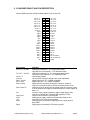
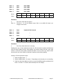
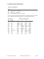
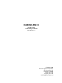
DIAMOND-MM-16 PC/104 Format 16-Bit Analog I/O Module User Manual V1.1 Copyright 1998 Diamond Systems Corporation 450 San Antonio Rd. Palo Alto, CA 94306 Tel (650) 813-1100 Fax (650) 813-1130 [email protected] TABLE OF CONTENTS 1. DESCRIPTION................................................................................................................................ 3 2. I/O HEADER PINOUT AND PIN DESCRIPTION........................................................................ 4 3. BOARD CONFIGURATION .......................................................................................................... 5 4. DIAMOND-MM-16 BOARD DRAWING ...................................................................................... 7 5. I/O MAP........................................................................................................................................... 8 6. REGISTER DEFINITIONS ............................................................................................................ 9 7. ANALOG INPUT RANGES AND RESOLUTION ...................................................................... 15 8. PERFORMING AN A/D CONVERSION ..................................................................................... 19 9. ANALOG OUTPUT RANGES AND RESOLUTION .................................................................. 21 10. GENERATING AN ANALOG OUTPUT ..................................................................................... 22 11. DIGITAL I/O OPERATION ......................................................................................................... 24 12. CALIBRATION PROCEDURE.................................................................................................... 25 13. PROGRAMMING ......................................................................................................................... 27 14. USING THE DRIVER SOFTWARE ............................................................................................ 27 15. DRIVER FUNCTION LIST .......................................................................................................... 28 16. ERROR CODE LIST..................................................................................................................... 28 17. DRIVER FUNCTION DESCRIPTIONS....................................................................................... 29 18. MISCELLANEOUS FUNCTIONS ............................................................................................... 40 19. TECHNICAL SUPPORT .............................................................................................................. 40 20. SPECIFICATIONS ........................................................................................................................ 41 1998 Diamond Systems Corp. Diamond-MM-16 User Manual V1.1 Page 2 DIAMOND-MM-16 PC/104 16-Bit Analog I/O Module 1. DESCRIPTION Diamond-MM-16 is a PC/104-format multifunction data acquisition board. It offers 16 singleended or 8 differential analog inputs with 16-bit resolution and programmable input range; 100,000 samples per second maximum sampling rate with DMA operation; 4 analog outputs with 12-bit resolution; user-adjustable analog output range; 8 bits of digital input; 8 bits of digital output; one 32-bit counter/timer for A/D conversion timing; and one 16-bit counter/timer for general purpose use. 1.1 Features Analog Inputs 16 single-ended / 8 differential analog input channels with 16-bit resolution Programmable gain, range, and polarity on inputs 100,000 samples per second maximum sampling rate on A/D Software, interrupt, and DMA A/D sampling control Analog Outputs 4 analog output channels with 12-bit resolution, 5mA max output current +/-15V @ +/-10mA output power for user circuitry +5V up to +10V @ up to 10mA precision reference output for sensors or user circuitry Note: total output current limited to 30mA Digital I/O 8 digital outputs 8 digital inputs Counter/Timers 1 32-bit counter/timer for A/D pacer clock 1 16-bit general purpose counter/timer 1998 Diamond Systems Corp. Diamond-MM-16 User Manual V1.1 Page 3 2. I/O HEADER PINOUT AND PIN DESCRIPTION Diamond-MM-6 provides a 50-pin header labeled J3 for all user I/O. Vin 15 / 7Vin 14 / 6Vin 13 / 5Vin 12 / 4Vin 11 / 3Vin 10 / 2Vin 9 / 1Vin 8 / 0Agnd Agnd Agnd Agnd -15V Agnd In 0Out 0 Dout 7 Dout 5 Dout 3 Dout 1 Din 7 Din 5 Din 3 Din 1 +5V Signal Name Vin 7/7+ ~ Vin 0/0+ Vin 15/7- ~ Vin 8/0Vout 0 - 3 Vref Out Dout7 - Dout0 Din7 - Din0 Din2 / Gate 0 Din0 / Gate 1/2 In0Out0, Out2 ±15V +5V Agnd Dgnd 1 3 5 7 9 11 13 15 17 19 21 23 25 27 29 31 33 35 37 39 41 43 45 47 49 2 4 6 8 10 12 14 16 18 20 22 24 26 28 30 32 34 36 38 40 42 44 46 48 50 Vin 7 / 7+ Vin 6 / 6+ Vin 5 / 5+ Vin 4 / 4+ Vin 3 / 3+ Vin 2 / 2+ Vin 1 / 1+ Vin 0 / 0+ Vref Out Vout 0 Vout 1 +15V Vout 2 Vout 3 Dgnd Out 2 Dout 6 Dout 4 Dout 2 Dout 0 Din 6 Din 4 Din 2 / Gate 0 Din 0 / Gate 1/2 Dgnd Definition Analog input channels 7 - 0 in single-ended mode; High side of input channels 7 - 0 in differential mode Analog input channels 15 - 8 in both single-ended mode; Low side of input channels 7 - 0 in differential mode 12-bit analog outputs +5V precision reference voltage output (user adjustable) Digital output port, TTL / CMOS compatible Digital input port, TTL / CMOS compatible Digital input line 2 doubles as the gate control for counter 0; Counter 0 counts when this line is high and holds when it is low Digital input line 0 can be used as a gate signal for counters 1 and 2 or as an external A/D trigger as determined by the control register at base + 11 Counter 0 input, negative polarity (negative edge trigger), also used as an external gate if external A/D triggering is used Counter 0 and Counter 2 output signals Analog power supply; maximum current draw 10mA per line Connected to PC/104 bus power supply Analog ground; connected to digital ground at a single point at device PS1 Digital ground; connected to PC/104 bus ground 1998 Diamond Systems Corp. Diamond-MM-16 User Manual V1.1 Page 4 3. BOARD CONFIGURATION Refer to the Drawing of Diamond-MM-16 in chapter 4 for locations of the configuration items mentioned here. 3.1 J8: Base Address Each board in the system must have a different base address. Diamond-MM-16's base address is set with pin header J8, located at the lower left corner of the board. Each of the four pairs of pins on J8 corresponds to a different address bit, as indicated underneath the header. An open location is equal to a 1, and an installed location is equal to a 0. The dipswitch is used to select address bits 9 - 6, resulting in an address decode on 64-byte boundaries. However, the board only occupies the lowermost 16 bytes of the selected address block. The table below lists the possible base address settings. The default setting is 300 Hex. Note that addresses below 100 Hex are not available for I/O devices. Base Address Hex 100 140 180 1C0 200 240 280 2C0 300 340 380 3C0 Decimal 256 320 384 448 512 576 640 704 768 (Default) 832 896 960 Pin Header J8 Configuration 9 Installed Installed Installed Installed Open Open Open Open Open Open Open Open 8 Open Open Open Open Installed Installed Installed Installed Open Open Open Open 7 Installed Installed Open Open Installed Installed Open Open Installed Installed Open Open 6 Installed Open Installed Open Installed Open Installed Open Installed Open Installed Open 3.2 J4: Single-Ended / Differential A/D Mode Single-ended mode: Both jumpers VERTICAL in upper position (over top & middle pins) Differential mode: Both jumpers VERTICAL in lower position (over middle & bottom pins) In Single-ended mode, Diamond-MM-16 has 16 input channels numbered 0 - 15. In Differential mode, Diamond-MM-16 has 8 input channels numbered 0 - 7. The high sides of the inputs are on pins 2 through 16 even, and the low sides of the inputs are on pins 1 through 15 odd. The default setting is Single-ended mode. 1998 Diamond Systems Corp. Diamond-MM-16 User Manual V1.1 Page 5 3.3 J5: Output Reference Voltage +5.000V: -5.000V: Jumper in left position Jumper in right position The default setting is +5.000V. 3.4 J6: Counter/Timer Input Clock Frequency 10MHz: 1MHz: Jumper in lower position Jumper in upper position The default is 1MHz. The selected frequency feeds the inputs of 82C54 counters 1 and 2. 3.5 J7: DMA Level Level 1: Level 3: Both jumpers installed HORIZONTALLY in RIGHT position Both jumpers installed HORIZONTALLY in LEFT position These jumpers are horizontal with respect to the board (parallel to the PC/104 connector). The default setting is Level 3. ⇒ NOTE: The circuit board markings are incorrect on V2 of this board. The left position is marked 1 but is actually level 3, and the right position is marked 3 but is actually level 1. 1998 Diamond Systems Corp. Diamond-MM-16 User Manual V1.1 Page 6 4. DIAMOND-MM-16 BOARD DRAWING 1998 Diamond Systems Corp. Diamond-MM-16 User Manual V1.1 Page 7 5. I/O MAP Diamond-MM-16 occupies 16 bytes in I/O space. These registers are described in detail in the next chapter. Base + 0 1 2 3 4 5 6 7 8 9 10 11 12 13 14 15 Write Function Start A/D conversion D/A LSB (all channels) A/D channel register Digital output port D/A 0 MSB D/A 1 MSB D/A 2 MSB D/A 3 MSB Clear interrupt flip flop Control register Counter/timer enable/select Analog range configuration Counter/timer 0 data register Counter/timer 1 data register Counter/timer 2 data register Counter/timer control register 1998 Diamond Systems Corp. Read Function A/D LSB (bits 7 - 0) A/D MSB (bits 15 - 8) A/D channel register Digital input port Update all D/A channels Update all D/A channels Update all D/A channels Update all D/A channels Status register Control register readback Not used Analog range readback Counter/timer 0 data register Counter/timer 1 data register Counter/timer 2 data register Counter/timer control register Diamond-MM-16 User Manual V1.1 Page 8 6. REGISTER DEFINITIONS Base + 0 Read A/D LSB + Channel Tag Bit No. 7 6 5 4 3 2 1 0 Name AD7 AD6 AD5 AD4 AD3 AD2 AD1 AD0 Definitions: AD7 - 0 Base + 1 A/D data bits 7 - 0; AD0 is the LSB Read A/D MSB Bit No. 7 6 5 4 3 2 1 0 Name AD11 AD10 AD9 AD8 AD7 AD6 AD5 AD4 Definitions: AD15 - 8 A/D data bits 15 - 8; AD15 is the MSB The A/D value is a twos complement 16-bit signed integer ranging from -32768 to +32767. The value is constructed from the two bytes at Base + 0 and Base + 1 by using the formula A/D value = (Base + 1) * 256 + (Base + 0) A reading of -32768 represents a negative full scale input (or below), and a reading of 32767 represents an input of positive full scale minus 1 LSB (or above). See Chapter 7 for formulas to convert the 16-bit A/D reading into the corresponding voltage. Base + 0 Write Start A/D Conversion Writing to Base + 0 starts an A/D conversion, unless a conversion is already in progress. The value written does not matter. Writing to Base + 0 will start an A/D conversion even if the board is set up for interrupt, DMA, or external trigger mode. 1998 Diamond Systems Corp. Diamond-MM-16 User Manual V1.1 Page 9 Base + 1 Write D/A LSB (All Channels) Bit No. 7 6 5 4 3 2 1 0 Name DA7 DA6 DA5 DA4 DA3 DA2 DA1 DA0 Definitions: DA7 - 0 Base + 2 D/A data bits 7 - 0 for the channel currently being accessed. This register is a holding register. Writing to it does not affect any D/A channel until the MSB is written. When the MSB is written (see below, Base + 4 through Base + 7), the value written to that register, along with the value written to this register, are simultaneously written to the D/A chip’s load register for the selected channel. A final read operation from Base + 7 is required to update the D/A with the new 12bit value. This final read operation is provided in order to enable simultaneous update of all 4 channels at once. Read/Write A/D Channel Register Bit No. 7 6 5 4 3 2 1 0 Name HIGH3 HIGH2 HIGH1 HIGH0 LOW3 LOW2 LOW1 LOW0 Definitions: HIGH3 - 0 High channel of channel scan range; ranges from 0 to 15 in single-ended mode, 0 - 7 in differential mode. LOW3 - 0 Low channel of channel scan range; ranges from 0 to 15 in single-ended mode, 0 - 7 in differential mode. Note: the high channel does not need to be higher than the low channel; for example, LOW = 8 and HIGH = 2 are valid settings. Base + 3 Write Digital Output Port Bit No. 7 6 5 4 3 2 1 0 Name DO7 DO6 DO5 DO4 DO3 DO2 DO1 DO0 These pins correspond directly to the same-named pins on I/O connector J3 (pins 33 - 40). On power-up or system reset, the digital output port is set to all zeroes. Base + 3 Read Digital Input Port Bit No. 7 6 5 4 3 2 1 0 Name DI7 DI6 DI5 DI4 DI3 DI2 DI1 DI0 These pins correspond directly to the same-named pins on I/O connector J3 (pins 41 - 48). 1998 Diamond Systems Corp. Diamond-MM-16 User Manual V1.1 Page 10 Base + 4 Write DAC 0 MSB Base + 5 Write DAC 1 MSB Base + 6 Write DAC 2 MSB Base + 7 Write DAC 3 MSB Bit No. 7 6 5 4 3 2 1 0 Name X X X X DA11 DA10 DA9 DA8 Definitions: X Don't Care; these bits are ignored DA11 - 8 D/A bits 11 - 8 for the selected output; DA11 is the MSB; D/A data is an unsigned 12-bit value. Base + 4 Read Update All D/A Channels Base + 5 Read “ Base + 6 Read “ Base + 7 Read “ Bit No. 7 6 5 4 3 2 1 0 Name X X X X X X X X Definitions: X Don't Care; these bits have no meaning Reading from any of these addresses causes all 4 D/A channels to update simultaneously with the values loaded into their load registers. Any channel which has had a new value written to it since the last update command will settle on its new value. Any channel which has not had a new value written will maintain its present value without glitching. Writing to a D/A requires three steps: 1. Write the LSB to base + 1. 2. Write the MSB to base + 4 to base + 7 depending on the channel you are controlling. 3. Read from the same address to which you wrote the MSB (actually any address from base + 4 to base + 7 will work, but this technique is a bit simpler). 1998 Diamond Systems Corp. Diamond-MM-16 User Manual V1.1 Page 11 Base + 8 Write Clear Interrupt Flip Flop Writing to this register clears the on-board interrupt flip flop. The value written does not matter. The interrupt flip flop is set whenever an interrupt is generated on Diamond-MM-16 (i.e. during A/D conversions), and it must be cleared by software before another interrupt can be generated. Diamond-MM-16's software driver includes an interrupt handler that performs this task automatically. Base + 8 Read Status Register Bit No. 7 6 5 4 3 2 1 0 Name STS U/B S/D INT ADCH3 ADCH2 ADCH1 ADCH0 STS A/D chip status: 1 A/D conversion in progress 0 A/D idle U/B Unipolar / Bipolar A/D input mode setting: 1 unipolar: A/D can measure only positive input voltages. 0 bipolar (default): A/D can measure both negative and positive input voltages. S/D Single-ended / Differential A/D input mode setting: 1 Single-ended (default) 0 Differential INT Interrupt request status: 1 Interrupt is pending; A/D has generated a new value 0 No interrupt is pending Note: A/D conversions continue to occur on schedule regardless of whether this bit is cleared. If a new conversion occurs before this bit is cleared, an overrun condition will occur, and the unread A/D value will be lost. There is no way to tell if an overrun condition has occurred. Therefore the programmer must ensure that the interrupt rate is not faster than the capability of the system and program to respond. ADCH3 - 0 Current A/D channel; this is the channel currently selected on board and is the channel that will be used for the next A/D conversion (unless a new value is written to the channel register). 1998 Diamond Systems Corp. Diamond-MM-16 User Manual V1.1 Page 12 Base + 9 Read/Write Control Register Bit No. 7 6 5 4 3 2 Name INTE INT2 INT1 INT0 X DMAEN 1 0 TRIGE INTTRIG INTE Interrupt enable: 1 Enable interrupts 0 Disable interrupts INT2 - 0 Interrupt level select: 011 = level 3, 100 = level 4, etc. INT2 is the MSB. Only levels 2 - 7 are valid; levels 0 and 1 are not connected on the board. X Don’t Care; the value of this bit is ignored. DMAEN DMA enable (DMA operation is explained later in this manual): 1 Enable DMA operation 0 Disable DMA operation TRIGE Enable hardware A/D trigger: 1 Enable hardware trigger (source is selected with INTTRIG bit) 0 Disable hardware trigger INTTRIG A/D trigger select: 1 Internal trigger: Rising edges on the output of counter/timer 2 (82C54) generate A/D conversions 0 External trigger: Falling edges on DI0 / Trigger, pin 48 on I/O connector J3, generate A/D conversions. Base + 10 Write Counter/Timer Control Register Bit No. 7 6 5 4 3 2 1 0 Name X X X X X C2 C1 C0 C2 External gate enable: 1 IN0- (pin 29 on the I/O header) acts as a gate for A/D sample control when external A/D clock is enabled (INTTRIG = 0 above). When IN0- is high, falling edges on DI0 (pin 48 on the I/O header) will initiate A/D conversions. When IN0- is low, the DI0 signal is inhibited. IN0- is connected to a 10KΩ pullup resistor. 0 IN0- does not act as a gate for external A/D clocking. C1 Counter 0 input source: 1 Input to Counter 0 is a 100kHz on-board reference frequency derived from the 10MHz oscillator. IN0- (pin 29 on the I/O header) gates this signal. When it is high (default), the 100kHz signal runs. When it is low, the 100kHz signal is stopped. 0 Input to Counter 0 is an inverted polarity copy of IN0-. IN0- is connected to a 10KΩ pull-up resistor. C0 Counters 1 and 2 gate control: 1 Counters 1 and 2 are gated by DI0 (pin 48 on the I/O header). When DI0 is low PRIOR TO THE START OF DMA CONVERSIONS, A/D conversions will not occur until it is brought high. DI0 is connected to a 10KΩ pullup resistor. 0 Counters 1 and 2 run freely with no gating. 1998 Diamond Systems Corp. Diamond-MM-16 User Manual V1.1 Page 13 Base + 11 Write Analog Configuration Register Bit No. 7 6 5 4 3 2 1 0 Name X X X DABU RANGE ADBU G1 G0 DABU D/A bipolar / unipolar setting; 0 = bipolar, 1 = unipolar RANGE 5V or 10V A/D positive full-scale voltage ADBU A/D bipolar / unipolar setting; 0 = bipolar, 1 = unipolar The table below lists the effects of the various combinations of ADBU and RANGE: RANGE 0 0 1 1 G1 - 0 ADBU 0 1 0 1 A/D full-scale range ±5V Invalid setting ±10V 0 - 10V A/D gain setting: G1 0 0 1 1 G0 0 1 0 1 Gain 1 2 4 8 The gain setting is the ratio between the A/D full-scale range and the effective input signal range. For example, if the A/D full-scale range is 0 - 10V, a gain setting of 2 creates an input signal range of 0 - 5V, and a gain setting of 4 creates an input signal range of 0 - 2.5V. ⇒: On power up or system reset, the board is configured for D/A bipolar mode, A/D bipolar mode, input range ±5V, gain of 1. Base + 11 Read Test Readback Register Bit No. 7 6 5 4 3 2 1 0 Name EQUAL C1 C0 DABU RANGE ADBU G1 G0 This address provides a means of reading back the values written to the registers at Base + 10 and Base + 11. Base + 12 ~ Base + 15 Read/Write 82C54 Counter/Timer Registers These registers map directly to the 82C54. The definitions of these registers can be found in the 82C54 datasheet appended to the back of this manual. 1998 Diamond Systems Corp. Diamond-MM-16 User Manual V1.1 Page 14 7. ANALOG INPUT RANGES AND RESOLUTION 7.1 Resolution Diamond-MM-16 uses a 16-bit A/D converter. This means that the analog input voltage can be measured to the precision of a 16-bit binary number. The maximum value of a 16-bit binary number is 216 - 1, or 65535, so the full range of numerical values that you can get from a Diamond-MM-16 analog input channel is 0 - 65535. The smallest change in input voltage that can be detected is 1/(216), or 1/65536, of the fullscale input range. This smallest change results in an increase or decrease of 1 in the A/D code, and so this change is referred to as 1 LSB, or 1 least significant bit. 7.2 Unipolar and Bipolar Inputs Diamond-MM-16 can measure both unipolar (positive only) and bipolar (positive and negative) analog voltages. The full-scale input voltage range depends on the Gain, Range, and Polarity bit settings in the Analog Configuration Register at base + 11. In front of the A/D converter is a programmable gain amplifier that multiplies the input signal before it reaches the A/D. This gain circuit has the effect of scaling the input voltage range to match the A/D converter for better resolution. In general you should select the highest gain you can that will allow the A/D converter to read the full range of voltages over which your input signals will vary. However, if you pick too high a gain, then the A/D converter will clip at either the high end or low end, and you will not be able to read the full range of voltages on your input signals. 7.3 Single Ended and Differential Inputs Diamond-MM-16 can handle both single-ended and differential inputs. A single-ended input is a single-wire input that is referenced to analog ground on the board. This means that the input voltage will be measured with respect to the board’s analog ground. A differential input is a two-wire input, and the board will measure the difference between the voltages of the two inputs. Polarity is important for a differential input. Diamond-MM-16 will subtract the voltage on the low (-) input from the voltage of the high (+) input. Differential inputs are frequently used when the grounds of the input device and the measurement device (Diamond-MM-16) are at different voltages, or when a low-level signal is being measured that has its own ground wire. A 16-bit A/D converter is extremely sensitive to noise and ground currents, so differential measurements are recommended whenever possible. Jumper block J4 is used to select single-ended or differential mode.To select single-ended more, insert the two jumpers vertically over the top and middle pins, and to select differential mode, insert the two jumpers vertically over the bottom and middle pins. 1998 Diamond Systems Corp. Diamond-MM-16 User Manual V1.1 Page 15 7.4 Input Ranges and Resolution Here is a table describing the full-scale input range for each possible analog input configuration. The parameters Polarity, Range, and Gain are combined to create the value “Code”, which is the value that you must write to the analog configuration register at Base + 11 to get the input range shown. A total of 9 different input ranges are possible. Note that the range programming codes 4, 5, 6, and 7 are invalid. Table 7.1 Polarity Bipolar Bipolar Bipolar Bipolar Unipolar Unipolar Unipolar Unipolar Bipolar Bipolar Bipolar Bipolar Unipolar Unipolar Unipolar Unipolar Range 5V 5V 5V 5V 5V 5V 5V 5V 10V 10V 10V 10V 10V 10V 10V 10V 1998 Diamond Systems Corp. Gain 1 2 4 8 1 2 4 8 1 2 4 8 1 2 4 8 Code 0 1 2 3 4 5 6 7 8 9 10 11 12 13 14 15 Full-Scale Range Resolution (1 LSB) ±5V 153 µV ±2.5V 76 µV ±1.25V 38 µV ±0.625V 19 µV Invalid setting Invalid setting Invalid setting Invalid setting ±10V 305 µV ±5V 153 µV ±2.5V 76 µV ±1.25V 38 µV 0 - 10V 153 µV 0 - 5V 76 µV 0 - 2.5V 38 µV 0 - 1.25V 19 µV Diamond-MM-16 User Manual V1.1 Page 16 7.5 A/D Conversion Formulas The 16-bit value returned by the A/D converter is always a twos complement number ranging from -32768 to 32767, regardless of the input range. This is because the input range of the A/D is fixed at ±10V. The input signal is actually magnified and shifted to match this range before it reaches the A/D. For example, for an input range of 0-10V, the signal is first shifted down by 5V to ±5V and then amplified by 2 to become ±10V. Therefore, two different formulas are needed to convert the A/D value back to a voltage, one for bipolar ranges, and one for unipolar ranges. Tables showing the correlation between A/D code and input voltage are shown on the following page. For bipolar input ranges: FS = full-scale voltage (e.g. 5V for ±5V range) If using a 16-bit signed integer in C: Input voltage = (A/D code / 32768) x FS Example: ±5V range selected, A/D code = 17762 (Hex 4560) Input voltage = (17762 / 32768) x 5V = +2.7103V Example: ±5V range selected, A/D code = -15008 (Hex C560) Input voltage = (-15008 / 32768) x 5V = -2.2900V If using a 32-bit signed integer in C, or unsigned or floating value in C or Basic: Input voltage = (A/D code / 32768) x FS If input voltage >= FS then input voltage = input voltage - 2 x FS Example: ±5V range selected, A/D code = 17762 (Hex 4560) Input voltage = (17762 / 32768) x 5V = +2.7103V Example: ±5V range selected, A/D code = 50528 (Hex C560) Input voltage = (50528 / 32768) x 5V = +7.7100V Since 7.7100V >= 5V, we must subtract: Input voltage = 7.7100V - 2 x 5V = -2.2900V For unipolar input ranges: FS = full-scale voltage (e.g. 10 for 0 - 10V range) Input voltage = (A/D code + 32768 / 65536) x FS Example: 0 - 10V range selected, A/D code = 17762 (Hex 4560) Input voltage = ((17762 + 32768) / 65536) x 10V = +7.7103V Note that this is simply the result for the ±5V range shifted up by 5V. 1998 Diamond Systems Corp. Diamond-MM-16 User Manual V1.1 Page 17 7.6 Correlation between A/D Code and Input Voltage The two tables below illustrate the correlation between the A/D code and the corresponding input voltage. Use these tables as guides to help think about how to convert between the voltage domain and the A/D code domain. Bipolar Input Ranges: A/D Code -32768 -32767 -1 0 1 32767 Input voltage formula -VFS -VFS + 1 LSB -1 LSB 0V +1 LSB VFS - 1 LSB Input voltage (± ± 5V range) -5.0000V -4.9998V -0.153mV 0.0000V 0.153mV 4.9998V Unipolar Input Ranges: A/D Code -32768 -32767 -1 0 1 32767 Input voltage formula 0V 1 LSB (VFS / 65536) VFS / 2 - 1 LSB VFS / 2 VFS / 2 + 1 LSB VFS - 1 LSB 1998 Diamond Systems Corp. Input voltage (0 - 10V range) 0.0000V 0.153mV 4.99985V 5.0000V 5.00015V 9.9998V Diamond-MM-16 User Manual V1.1 Page 18 8. PERFORMING AN A/D CONVERSION This chapter describes the steps involved in performing an A/D conversion on a selected input channel using direct programming (not with the driver software). There are six steps involved in performing an A/D conversion: 1. Select the input channel 2. Select the input range (Range, Polarity, and Gain codes) 3. Start an A/D conversion on the current channel 4. Wait for the conversion to finish 5. Read the data 6. Convert the numerical data to a meaningful value 8.1 Select the input channel To select the input channel to read, write a low-channel/high-channel pair to the channel register at base + 2. (See Chapter 7). The low 4 bits select the low channel, and the high 4 bits select the high channel. When you write to this register, the current channel is set to the low channel. ⇒ Note: When you perform an A/D conversion, the current channel register on the board is automatically incremented to the next channel in the selected range. Therefore, to perform A/D conversions on a group of consecutively-numbered channels, you do not need to write the input channel prior to each conversion. For example, to read from channels 0 - 2, write Hex 20 to base + 2. The first conversion is on channel 0, the second will be on channel 1, and the third will be on channel 2. Then the channel counter wraps around to the beginning again, so the fourth conversion will be on channel 0 again, and so on. This happens automatically without any further channel setting required. 8.2 Select the input range Select the code from Table 7.1 corresponding to the desired input range and write it to the analog I/O control register at Base + 11. You only need to write to this register if you want to select a different input range from the one used for the previous conversion. ⇒ Note: You can read the current value of this register by reading from Base + 11. There is one more bit in this register that corresponds to the D/A mode, so you should be careful not to erase this bit accidentally if it has been previously set. 8.3 Start an A/D conversion on the current channel After selecting the channel register and/or the input range, about 10 microseconds is required as a settling time for the analog front end circuitry. You can implement this delay as a short software loop. After waiting for the analog circuitry to settle, you can perform an A/D conversion on the selected channel. To do this, simply write to base + 0 to start the conversion. The value you write does not matter and is ignored. 1998 Diamond Systems Corp. Diamond-MM-16 User Manual V1.1 Page 19 8.4 Wait for the conversion to finish The A/D converter takes up to 10 microseconds to complete a conversion. Most processors and software can operate fast enough so that if you try to read the A/D converter immediately after writing to base + 0, you will beat the A/D converter and get invalid data. Therefore the A/D converter provides a status signal to indicate whether it is busy or idle. This bit can be read back as bit 7 in the status register at base + 8. When the A/D converter is busy (performing an A/D conversion), this bit is 1, and when the A/D converter is idle (conversion is done and data is available), this bit is 0. Here is a pseudocode explanation: Status = read(base+8) AND 128 ;or Status = read(base+8) AND 80 Hex If Status = 0 then conversion is complete, else A/D converter is busy Keep repeating this procedure until Status = 0. 8.5 Read the data Once the conversion is complete, you can read the data back from the A/D converter. The data is 16 bits wide and is read back in two 8-bit bytes. Refer to the register definitions on p. 8 for the format of the A/D data. The following pseudocode illustrates how to construct the 16-bit A/D value from these two bytes: LSB = read(base) MSB = read(base+1) Data = MSB * 256 + LSB ;Get low 8 bits ;Get high 8 bits ;Combine the 2 bytes into a 16-bit value The final data ranges from 0 to 65535 (0 to 216 - 1) as an unsigned integer. This value must be interpreted as a signed integer ranging from -32768 to +32767. 8.6 Convert the numerical data to a meaningful value Once you have the A/D value, you need to convert it to a meaningful value. The first step is to convert it back to the actual measured voltage. Afterwards you may need to convert the voltage to some other engineering units (for example, the voltage may come from a temperature sensor, and then you would need to convert the voltage to the corresponding temperature according to the temperature sensor’s characteristics). Both of these conversions can be done simultaneously by combining them into a single conversion formula. See Section 7.5 on Page 17 for an explanation on converting A/D codes to input voltage and the required formulas. Although the A/D data range always includes both negative and positive values, the input voltage may be unipolar, requiring an offset to be added in during the conversion calculation. 1998 Diamond Systems Corp. Diamond-MM-16 User Manual V1.1 Page 20 9. ANALOG OUTPUT RANGES AND RESOLUTION 9.1 Description Diamond-MM-16 uses a four-channel 12-bit D/A converter (DAC) to provide four analog outputs. A 12-bit DAC can generate output voltages with the precision of a 12-bit binary number. The maximum value of a 12-bit binary number is 212 - 1, or 4095, so the full range of numerical values that you can write to the analog outputs on Diamond-MM-16 is 0 - 4095. ⇒ Note: In this manual, the terms analog output, D/A, and DAC are all used interchangeably to mean the same thing. 9.2 Resolution The resolution is the smallest possible change in output voltage. For a 12-bit DAC the resolution is 1/(212), or 1/4096, of the full-scale output range. This smallest change results from an increase or decrease of 1 in the D/A code, and so this change is referred to as 1 LSB, or 1 least significant bit. The value of this LSB is calculated as follows: 1 LSB = Full-scale output voltage / 4096 Example: Full-scale output voltage = 5V 1 LSB = 5V / 4096 = 1.22mV 9.3 Full-ScaleRange Selection The D/A converter chip on Diamond-MM-16 requires two references, one for the low end and one for the high end of the range. The high end can be set to any value between 5V and 10V, and the low end can be either 0V (for unipolar output ranges) or minus the high end voltage. Potentiometer R8 is used to select the high end reference voltage. It is preset to 5V. To select a different value, first move the jumper in J5 (above the D/A converter IC and near the I/O header) so that it is over the middle and right pins. Then connect a voltmeter to pin 18 on the I/O header and adjust R8 until the desired full-scale voltage is achieved. The low end voltage is selected in software with bit 4 in the analog configuration register at base + 11. When this bit is 0, the D/A is set for bipolar mode (low reference = - high reference), and when this bit is 1, the D/A is set for unipolar mode (low reference = 0V). On power up, this entire register is cleared, so the power-up mode is always bipolar mode. In addition, on power up, the D/A automatically resets to mid-scale, which is 0V in bipolar mode, so on power up all D/A channels are set to 0V. 1998 Diamond Systems Corp. Diamond-MM-16 User Manual V1.1 Page 21 10. GENERATING AN ANALOG OUTPUT This chapter describes the steps involved in generating an analog output (also called performing a D/A conversion) on a selected output channel using direct programming (not with the driver software). There are two steps involved in performing a D/A conversion: 1. Compute the D/A output value for the desired output voltage 2. Compute the LSB and MSB values 3. Write the value to the selected output channel 10.1 Compute the D/A code for the desired output voltage A different formula is required for bipolar and unipolar output ranges. Use the following formula to compute the D/A code in unipolar mode: Output value = Output voltage / Full-scale voltage * 4096 Example: Desired output voltage = 2.168V, full-scale voltage = 5V, unipolar mode (0-5V) Output code = 2.168V / 5V * 4096 = 1776 Use the following formula to compute the D/A code in bipolar mode: Output value = Output voltage / Full-scale voltage * 2048 + 2048 Example: Desired output voltage = -2.168V, full-scale voltage = 5V, bipolar mode (±5V) Output code = -2.168V / 5V * 2048 + 2048 = 1160 ⇒ Note: The DAC cannot generate the actual full-scale reference voltage; to do so would require an output code of 4096, which is not possible with a 12-bit number. The maximum output value is 4095. Therefore the maximum possible output voltage is 1 LSB less than the full-scale reference voltage. 10.2 Compute the LSB and MSB values Use the following formulas to compute the LSB and MSB values: LSB = D/A Code AND 255 ;keep only the low 8 bits MSB = int(D/A code / 256) ;strip off low 8 bits, keep 4 high bits Example: Output code = 1776 LSB = 1776 AND 255 = 240 (F0 Hex) MSB = int(1776 / 256) = int(6.9375) = 6 (In other words, 1776 = 6*256 + 240) 1998 Diamond Systems Corp. Diamond-MM-16 User Manual V1.1 Page 22 10.3 Write the value to the selected output channel The LSB for all channels is written to base + 1, while the MSB is written to address base + 4 through base + 7 for channel 0 through 3, respectively. Here are the relevant portions of the I/O map: Base + ... 1 ... 4 5 6 7 ... Write Function ... D/A LSB (all channels) ... D/A 0 MSB D/A 1 MSB D/A 2 MSB D/A 3 MSB ... Read Function ... A/D MSB (bits 15 - 8) ... Update all D/A channels Update all D/A channels Update all D/A channels Update all D/A channels ... The register at base + 1 is actually a holding register, and the value in it does not reach the DAC until the MSB is written. When the MSB is written, all 12 bits are loaded simultaneously into the selected DAC channel. Therefore, you must write the LSB first. At this point the DAC will still remain at its current output voltage. To update the DAC to its new output voltage, you must perform a read operation from any address in the range base + 4 through base + 7. The value read is not meaningful. This read operation actually updates all 4 channels simultaneously, allowing synchronization of the update time for multiple channels. Any channel that does not have a new value loaded into it will remain stable at its current value, and any channel that has new data loaded into it will update to its new value. Example: Write a value of 1776 to channel 1 From above, LSB = 240, MSB = 6 1. Write 240 to base + 1 2. Then write 6 to base + 5 3. Then read from base + 5 to update the DAC 1998 Diamond Systems Corp. Diamond-MM-16 User Manual V1.1 Page 23 11. DIGITAL I/O OPERATION Diamond-MM-16 contains an 8-bit digital output port and an 8-bit digital input port. Both ports are located at base + 3. To access the output lines, simply write an 8-bit value to base + 3. Similarly, to read the input lines, read from base + 3. The output lines are located at pins 33 through 40 on the I/O header J3 (see Chapter 2, p. 4). They are CMOS/TTL compatible and can drive up to ±6mA max per line. They do not have a readback feature, so your program must keep track of the latest output value. The inputs are located at pins 41 through 48 on the I/O header J3. They are also CMOS/TTL compatible. There is no latch signal provided. However, the values are latched when being read to prevent transitions during the CPU read operation. Input line 2 doubles as the gate control for counter 0. When it is high, counter 0 can count, and when it is low, counter 0 holds its present value. This line has a 10KΩ pull-up resistor on board to force it to a default high state to enable counter 0 when there is no input signal connected. Input line 0 doubles as a programmable gate control for counters 1 and 2. These counters are combined together and used as the A/D pacer clock. Bit 0 of the counter/timer control register at base + 10 determines whether these counters run freely or whether Input line 0 is the gate (see Chapter 6, page 13). This line also has a 10KΩ pull-up resistor. 1998 Diamond Systems Corp. Diamond-MM-16 User Manual V1.1 Page 24 12. CALIBRATION PROCEDURE All boards are calibrated at the factory prior to shipment for ±10V input range with a gain of 1 and +/-5V output range. Minor offsets and gain errors will occur when using different ranges. However these errors may not be significant enough to require recalibration, since most adjustments can be performed in software. Recalibration is needed primarily if you want to change the D/A range or if you want to achieve higher precision for a different A/D range. To calibrate the board, you will need a voltmeter with a precision of at least 5 1/2 digits and a precision voltage source. In place of the voltage source you can use the analog outputs on Diamond-MM-16 after they have been calibrated, but you may have to make adjustments to the target A/D readings since the D/A only has 12 bits of resolution. Note that there are three test points on the board near the top edge. These are marked with squares on the silkscreen and are labeled 1, 2, 3. These test points are used in the calibration procedure. Refer to the board diagram on page 7 for the location of the potentiometers mentioned here. For all analog input measurements, single-ended inputs are assumed (jumpers in J4 are in the top position). 12.1 Gain Amplifier Output Offset Adjust Connect channel 0 to analog ground (wire J3 pin 17 to J3 pin 16). Select channel 0 as the current input channel (write 0 to base + 2). Select a gain of 1 (write 0 to base + 11). Connect the voltmeter to test point 1 and adjust R6 until the meter reads 0.000V. 12.2 Gain Amplifier Input Offset Adjust Connect channel 0 to analog ground (wire J3 pin 17 to J3 pin 16). Select channel 0 as the current input channel (write 0 to base + 2). Select a gain of 8 (write 3 to base + 11). Connect the voltmeter to test point 1 and adjust R7 until the meter reads 0.000V. ⇒ Note: Steps 12.1 and 12.2 affect each other, so several iterations may be necessary to converge on a 0V measurement for both adjustments. 12.3 A/D ± 5V Range Gain Adjust Jumper on J5 needs to be installed over the middle and left pins. Connect the voltmeter to the reference output pin on the I/O header (J3 pin 18) and measure the voltage. It will be in the range 5.000V ±2.5mV. Connect channel 0 to the output reference (wire J3 pin 18 to J3 pin 16). Select channel 0 as the current input channel (write 0 to base + 2). Select a gain of 1 and ±5V range (write 0 to base + 11). Connect the voltmeter to test point 2 and adjust R5 until the meter reads 2 times the reference voltage measured above (approximately 10.000V). 1998 Diamond Systems Corp. Diamond-MM-16 User Manual V1.1 Page 25 12.4 A/D Unipolar Range Offset Adjust Connect channel 0 to analog ground (wire J3 pin 16 to J3 pin 17). Select channel 0 as the current input channel (write 0 to base + 2). Select a gain of 1 and 0-10V range (write 12 to base + 11). Connect the voltmeter to test point 3 and adjust R4 until the meter reads -10.000V. 12.5 A/D Unipolar Range Gain Adjust Connect channel 0 to the output reference (wire J3 pin 16 to J3 pin 18). Select channel 0 as the current input channel (write 0 to base + 2). Select a gain of 1 and 0-10V range (write 12 to base + 11). Connect the voltmeter to test point 3 and adjust R3 until the meter reads 2 times the reference voltage measured above minus 10V (or approximately 0V). 12.6 A/D Offset Adjust Connect channel 0 to analog ground (wire J3 pin 17 to J3 pin 16). Select channel 0 as the current input channel (write 0 to base + 2). Select a gain of 1 and ±10V range (write 8 to base + 11). Perform A/D conversions and adjust R1 until the A/D readings are centered around 0. 12.7 A/D Gain Adjust Connect channel 0 to 9.999V. Select channel 0 as the current input channel (write 0 to base + 2). Select a gain of 1 and ±10V range (write 8 to base + 11). Perform multiple A/D conversions and adjust R2 until the A/D readings average 32765. 12.8 D/A Positive Full-Scale Reference Jumper on J5 needs to be installed over the middle and right pins. Connect the voltmeter to J3 pin 18 and adjust R8 until the meter reads +5.000V. If you are setting the analog output full scale range to a voltage other than +5V, then adjust R8 to obtain that voltage now. 12.9 D/A Bipolar Mode Negative Full-Scale Reference Write 0 to all four D/A channels to set them at their negative full scale value. Set the DACs for bipolar mode (write 0 to base + 11). Adjust R9 until the four outputs are as close as possible to minus the full-scale reference adjusted in step 12.8. For example, if you are calibrating for a 5V full-scale D/A range, then adjust R9 until the four outputs are as close as possible to -5.000V. Note that there are small offsets in each output, so each output will deviate somewhat (not more than 2LSB) from the exact value. 1998 Diamond Systems Corp. Diamond-MM-16 User Manual V1.1 Page 26 13. PROGRAMMING Two methods of programming are possible: either direct access using port read and write statements, or using the driver software. Diamond-MM-16 is a relatively simple board to program, so you may prefer to avoid the driver and just use port commands. However, if you are planning to use interrupts, you will most likely find it far simpler to use the driver's built-in interrupt support than to write your own interrupt routine and handle the interrupt vectors. To program Diamond-MM-16 directly in C, use the following code: Input: a = inp(addr); Output: outp(addr,a); To program Diamond-MM-16 directly in Basic, use the following code: Input: A = INP(ADDR) Output: OUT ADDR,A In both examples, "a" is the data and "addr" is the address of the port (base address plus offset). The control register must be programmed to set the direction of the ports being used. Upon power-up or system reset, all ports are set to input, and all output registers are set to 0. The output registers can be written to regardless of the direction of the ports. If you are using some ports as outputs, you may want to write initial values into the output registers before you set those ports to output mode; this way, when you set the direction to output, the signal lines go from high-impedance (tri-state) directly to the correct initial value. If you set a port to output without first loading its output register, whatever is in the register will appear on the output pins. This could cause problems depending on your external circuit. 14. USING THE DRIVER SOFTWARE Driver software is included to enable interfacing Diamond-MM-16 to user programs. Four versions are available for the Small, Compact, Medium, and Large models of Microsoft C 5.0 and later and QuickC version 2.0 and later. The respective file names are DMM16CS.OBJ, DMM16CC.OBJ, DMM16CM.OBJ, and DMM16CL.OBJ. The function is declared in file DMM16.H. Basic drivers are also included: for GW-BASIC, the file is DMM16.BIN, and for QuickBASIC, the file is DMM16.OBJ. The driver contains a function call to simplify programming Diamond-MM-16. The interface is as follows: In C: dmm16(f,d); In Basic: CALL DMM16(F%,D%(0)) where dmm16() is the function name, f or f% is an integer containing the function number, and d[] or D%() is an integer array (size 17 elements) containing parameters and return data specific to the function number. For GW-BASIC programs, you must load the driver into free memory at the start of your program, as follows: 10 DEF SEG = &H4000 20 BLOAD "DMM16.BIN",0 1998 Diamond Systems Corp. example of free area, can be changed load driver at address 40000 hex (segment 4000, offset 0) Diamond-MM-16 User Manual V1.1 Page 27 15. DRIVER FUNCTION LIST In the descriptions below, Input means data passed to the function and Output means data returned from the function. Function 0 is an initializing function and must be the first DMM16 call in any program. The functions are grouped by type: 0 is initialization, 1 - 19 are analog input, 20 - 39 are analog output, 40 - 59 are digital, and 80 - 99 are auxiliary. Not all function numbers are assigned. The current DMM16 functions are: No. 0 1 2 3 4 5 9 20 21 41 42 45 46 47 48 61 62 63 80 81 82 Function Description Initialize board and driver Perform single A/D conversion Perform A/D scan, up to 16 channels Perform interrupt-driven A/D conversions Perform interrupt-driven A/D scans Perform DMA-driven A/D conversions (fastest possible rates) Return current analog I/O settings Perform D/A conversion on one channel Perform D/A conversion on all four channels Digital byte input Digital byte output Bit input Bit set/reset Interrupt-driven digital input Interrupt-driven digital output Program counter/timer Counter/timer readback Direct counter/timer access Data transfer between array and memory buffer for digital I/O operations Interrupt/DMA operation statistics Halt/resume interrupt/DMA operation Page 29 30 30 31 31 31 33 33 33 34 34 34 34 35 35 36 37 37 38 39 39 16. ERROR CODE LIST An Error code is returned in d[0] after each function call. Generally, all arguments are checked for validity before the function executes. However, certain arguments, such as pointer values, are not checked, so caution is advised when using pointers, since an invalid pointer can corrupt memory or crash the system when the program attempts to write data to the referenced memory location. Code 0 1-12 20 21 22 23 24 Error No error, function executed properly Value n in array d[] has an invalid value; check specifications Invalid function number Driver not initialized; must use Function 0 first Hardware error; possible incorrect base address setting Background operation cannot start because another one is already running Cannot resume background operation because none was running/suspended 1998 Diamond Systems Corp. Diamond-MM-16 User Manual V1.1 Page 28 17. DRIVER FUNCTION DESCRIPTIONS Function 0: Initialize Board Inputs d[1] d[2] d[3] d[4] Base address (see list below) Interrupt level, 2 - 7 (default is 5) DMA level, 1 or 3 (default is 3) D/A polarity setting: 0 = bipolar, 1 = unipolar Function 0 must be the first dmm16() function call in any program using the driver. It gives the driver information about Diamond-MM-16 for use in subsequent function calls. Base Address Hex 100 140 180 1C0 200 240 280 2C0 300 340 380 3C0 Decimal 256 320 384 448 512 576 640 704 768 (Default) 832 896 960 1998 Diamond Systems Corp. Pin Header J8 Configuration 9 Installed Installed Installed Installed Open Open Open Open Open Open Open Open 8 Open Open Open Open Installed Installed Installed Installed Open Open Open Open 7 Installed Installed Open Open Installed Installed Open Open Installed Installed Open Open 6 Installed Open Installed Open Installed Open Installed Open Installed Open Installed Open Diamond-MM-16 User Manual V1.1 Page 29 Function 1: Single A/D conversion Inputs d[2] Channel no., 0 - 15 d[3] Gain code: Code Gain 0 1 1 2 2 4 3 8 d[4] Full scale range code: Code Range 0 ±5V 1 ±10V 2 0-10V Output d[1] A/D code, -32768 - 32767 Function 1 performs a single A/D conversion on the selected channel. The result is returned in d[1]. Note that the value is always twos complement, even though the input range may be set for unipolar voltages. See Section 7.5 on page 17 for conversion formulas to compute the input voltage from the A/D code. Function 2: Single A/D scan across channel range Inputs d[1] d[2] d[3] d[4] Low channel in scan range, 0 - 15 High channel in scan range, 0 - 15 Gain code (see table above) Full scale range code (see table above) Outputs d[1] A/D code for first channel in scan range ... ... d[n] A/D code for last channel in scan range; n <= 16 This function performs a single A/D conversion on the selected range of input channels. Up to 16 channels can be selected in the scan range, and the high channel must be higher than the low channel. 1998 Diamond Systems Corp. Diamond-MM-16 User Manual V1.1 Page 30 Function 3: Interrupt-driven single A/D conversions Function 4: Interrupt-driven A/D scans Function 5: DMA-driven single A/D conversions Inputs d[1] d[2] d[3] d[4] d[5] d[6] d[7] d[8] d[9] d[10] Number of conversions, 1 - 32767 Segment of memory buffer address or array (see text) Offset of memory buffer address or array (see text) Operation type: single-pass (0) or recycle (1) A/D clock source: 0: External A/D clock; falling edges on an external signal connected to DI0, pin 48 on the I/O header generate A/D conversions 1: Internal A/D clock; rising edges on the output of counter/timer no. 2 on the board generate A/D conversions Low channel in scan range, 0 - 15 High channel in scan range, 0 - 15 External A/D clock gate enable (used only when d[5] = 0): 0: No external gate on external A/D clock 1: External gate enabled on external A/D clock Gain code (see table on previous page) Full scale range code (see table on previous page) Functions 3 and 4 install an interrupt routine to acquire data in background mode and store it in a memory buffer. Function 5 uses the PC's DMA controller for high-speed transfers from the A/D to PC memory. In C, the buffer can be an integer array using the DSC functions get_segment(array) and get_offset(array) for d[2] and d[3] (see below, Miscellaneous Functions). The operation type indicator in d[4] determines how the memory buffer is used. If d[4] = 0, then d[1] conversions are performed and then interrupts/DMA transfers stop. If d[4] = 1, then after d[1] conversions, the internal buffer pointer is reset to the start, and future interrupts/DMA requests overwrite the buffer with new data. Thus the most recent d[1] conversions are always in memory, and the current position in the buffer can be acquired by using Function 81 below. The sequence of operations is as follows: The A/D clock source selected with d[5] (internal or external) generates an A/D conversion on the current channel and simultaneously increments the channel register to the next channel in the range selected by d[6] and d[7]. When the A/D conversion is complete, the data is transferred to the PC via either interrupt routine (Functions 3 and 4) or DMA cycle (Function 5). Note that there is no restriction on the selection of the low and high channels. Any combination of two channel numbers is valid. For example, 0 and 3 means that channels 0 3 will be read in sequence (4 channels), and 12 and 2 means that 7 channels will be read in sequence (12 - 15, then 0 - 2). If d[6] and d[7] are different, then the following applies: For function 3, each interrupt results in one new conversion on the current channel, and then the board switches to the next channel in the sequence for the next conversion. For function 4, each interrupt results in a reading of each channel in the scan range d[6] through d[7]. For function 5, each DMA cycle results in one new conversion on the current channel as in Function 3. If d[6] = d[7], then each interrupt or DMA operation results in a single conversion on the same channel. Function 4 with d[6] = d[7] is identical to Function 3 in operation. 1998 Diamond Systems Corp. Diamond-MM-16 User Manual V1.1 Page 31 Trigger source: Functions 3, 4, and 5 (as well as Functions 47 and 48 below) can be triggered either from the on-board counter/timer or from an external digital signal on pin 48 of the I/O header (signal DI0). If the counter/timer is used, then it must be programmed for the correct sample rate before Functions 3, 4, or 5 are called. See Function 61 for counter/timer programming. Note that the output of counter 2 is used to drive the interrupt or DMA operation, counter 2 is in turn driven by counter 1, and counter 1 is driven by either a 1MHz or 10MHz signal derived from the on-board clock oscillator. (J9 is used to select the frequency source.) Thus both counters 1 and 2 must be programmed to generate a time base for A/D conversions. The sample rate becomes: Rate = 1MHz (or 10MHz) / (counter 1 divider value x counter 2 divider value) If an external trigger is used, connect it to pin 48 (DI0) on the I/O header. This pin requires an active-low TTL signal to generate conversions. It is wired to a 10K ohm pull-up resistor, so just a pull-down to ground is required if the signal is being driven externally. The trigger is edge-sensitive; one A/D conversion (or scan) is performed for each low-going edge. Both Functions 3 and 4 can be used to acquire data at rates of up to about 20,000-30,000 samples per second. The actual upper limit is platform-dependent and can only be determined through experiment. For Function 5, the upper limit is approximately 100,000 samples per second, since the software overhead of the interrupt routine is eliminated. Again the actual limit is platform-dependent. External A/D clock gate: When d[7] = 1 and external A/D clock is enabled (d[5] = 0), signal IN0- (pin 29 on the I/O header) acts as a gate on the external A/D clock signal connected to DI0 (pin 48 on the I/O header). When IN0- is low, the external A/D clock is inhibited, and when IN0- is high, falling edges on the external signal generate A/D conversions. 1998 Diamond Systems Corp. Diamond-MM-16 User Manual V1.1 Page 32 Function 9: Return Current Analog Settings Outputs d[1] Current low channel no. setting, 0 - 15 d[2] Current high channel setting, 0 - 15 d[3] Current A/D gain code: Code Gain 0 1 1 2 2 4 3 8 d[4] Current A/D range code: Code Range 0 ±5V 1 ±10V 2 0-10V d[5] Current D/A polarity setting: 0 - bipolar, 1 = unipolar Function 9 returns the current settings programmed into the board. Function 20: Single D/A conversion Inputs d[1] D/A code, 0 - 4095 d[2] Channel, 0 - 3 Function 20 programs the selected D/A channel with the indicated code. See the formulas in Section 10.1 on page 22 for calculating the D/A code needed to produce the desired output voltage. Note that the unipolar/bipolar setting is not provided here, since if it is changed, then all four channels are affected. Therefore the D/A unipolar/bipolar setting should be done only once at program startup during the board initialization function (Function 0). Function 21: Simultaneous D/A output on 4 channels Inputs d[1] d[2] d[3] d[4] D/A code for channel 0, 0 - 4095 D/A code for channel 1, 0 - 4095 D/A code for channel 2, 0 - 4095 D/A code for channel 3, 0 - 4095 This function updates all four D/A channels simultaneously with the selected codes. See the formulas in Section 10.1 on page 22 for calculating the D/A code needed to produce the desired output voltage. 1998 Diamond Systems Corp. Diamond-MM-16 User Manual V1.1 Page 33 Function 41: Digital Byte Input Output d[1] Data from input port, range 0 - 255 Function 41 returns the 8-bit data appearing on the I/O header pins 41 - 48. Pin 41 contains the MSB (DI7), and pin 48 contains the LSB (DI0). Function 42: Digital Byte Output Input d[1] Output data, range 0 - 255 Function 42 writes the specified 8-bit data to the digital output port on I/O header pins 33 40. Pin 33 is the MSB (DO7), and pin 40 is the LSB (DO0). Only the lower 8 bits of the 16-bit integer variable d[1] are used for output; the remaining bits are ignored. Function 45: Bit Input Inputs d[2] Bit number, 0 - 7, corresponding to digital input lines DI0 - DI7 Output d[1] Bit value, 0 or 1 Function 45 returns the value of the selected bit in d[1]. Function 46: Bit Set/Reset Inputs d[1] Bit value, 0 or 1 d[2] Bit number, 0 - 7, corresponding to digital output lines DO0 - DO7 This function sets the selected output bit to the same value as the least significant bit of the value in d[1], i.e. if d[1] is even, the bit is set to 0, and if d[1] is odd, the bit is set to 1. The contents of the remaining bits on the output port are not disturbed. The driver software maintains copies of the contents of all the output registers on DiamondMM-16, but these copies are valid only as long as all access to the board is through the driver. As long as this condition is met, Function 46 will work correctly; however, if direct I/O commands to the output registers are mixed with function calls to those registers, Function 46 will have unpredictable results on the unselected bits. 1998 Diamond Systems Corp. Diamond-MM-16 User Manual V1.1 Page 34 Function 47: Interrupt-Driven Digital Input Function 48: Interrupt-Driven Digital Output Inputs d[1] Number of transfers, 1 - 32767 d[2] Size / bit number for I/O operation: 0 - 7 selects bit I/O on DI0-DI7 or DO0 - DO7 8 selects byte I/O, using entire DI or DO port d[3] Operation type: single-pass (0) or recycle (1) d[4] Trigger source (see page 19): 0 = external signal connected to DI0, pin 48 on the I/O header 1 = internal signal from the output of the counter/timer d[5] Segment of memory buffer address or array (see text) d[6] Offset of memory buffer address or array (see text) These functions install an interrupt routine to input or output digital data in background mode. Each falling edge on the selected trigger source will generate an interrupt request, resulting in one transfer of the specified type to/from the memory buffer or array. Interrupt operation takes over the A/D converter, so A/D conversions cannot be performed when digital I/O interrupts are in process. In C, the buffer can be an integer array using the DSC functions get_segment(array) and get_offset(array) for d[5] and d[6] (see below, Miscellaneous Functions). In Basic, the values for segment and offset must be specified as an address somewhere in free memory. A typical example is segment = &H4000 and offset = 0. For an input operation, typically the data is transferred to an integer array using Function 80 after Function 47 has been called and the interrupt operation is complete (or during the operation if recycle mode is selected). For an output operation, typically the data is placed in memory from an array by using Function 80 prior to using Function 48. The operation type indicator determines the use of this buffer. If d[4] = 0, then d[1] conversions are performed and then interrupts stop. If d[4] = 1, then after d[1] transfers, the internal buffer pointer is reset to the start, and future interrupts recommence from that position. Thus in input mode, the most recent d[1] input values are always in memory or the array, and in output mode, a periodic digital waveform with d[1] values will be output. The current position in the buffer can be acquired by using Function 81 (see below). 1998 Diamond Systems Corp. Diamond-MM-16 User Manual V1.1 Page 35 Function 61: Program Counter/Timer Inputs d[1] Counter no., 0 - 2 d[2] Counter mode, 0 - 5 d[3] Counter data, 16-bit integer This function programs the counter/timer for rate generator or counting functions. See the 8254 datasheet for counter mode definitions. The most common mode is 2, which implements a rate generator with a negative-going pulse one clock wide every n clocks, where n is the data in d[3]. The input to counter 2 is jumper-selected via J9 to either 1MHz or 10MHz, and the output of counter to 2 is connected to the input of counter 1. Thus the counter 2 / counter 1 combination provides a 32-bit divider for the 10MHz clock for interrupt and DMA operation timing. Counter 1's output can be selected as the trigger source for any interrupt or DMA operation, or an external signal can be used. If the counter/timer is used as the trigger source, remember that both counters 1 and 2 must be programmed. Normally Mode 2 is selected for these counters. The final operation rate is determined by the formula: Rate = 1MHz (or 10MHz) / (counter 1 divider value x counter 2 divider value) A complete 82C54 datasheet is provided at the back of this manual to assist in using the counter/timer circuit. 1998 Diamond Systems Corp. Diamond-MM-16 User Manual V1.1 Page 36 Function 62: Counter/Timer Readback Command Inputs d[1] Nonzero to read back Counter 0 data/status d[2] Nonzero to read back Counter 1 data/status d[3] Nonzero to read back Counter 2 data/status Outputs d[4] Current count value of counter 0 if selected, else 0 d[5] Current count value of counter 1 if selected, else 0 d[6] Current count value of counter 2 if selected, else 0 d[7] Current status of counter 0 if selected, else 0 d[8] Current status of counter 1 if selected, else 0 d[9] Current status of counter 2 if selected, else 0 This function implements the 8254 readback command. It will return the current contents of each counter's count register and the current state of each counter's output line. Function 63: Direct Counter Access Inputs d[1] Counter mode register value d[2] Counter data This function is provided for programming the counter/timer for modes not supported directly by Function 62. 1998 Diamond Systems Corp. Diamond-MM-16 User Manual V1.1 Page 37 Function 80: Data Transfer Between Memory and Program Array Inputs for C d[1] No. of transfers, 0 - 32767 d[2] Source data size: must be set to 1 for Diamond-MM-16 d[3] Segment portion of source address d[4] Offset portion of source address d[5] Destination data size: must be set to 1 for Diamond-MM-16 d[6] Segment portion of destination address d[7] Offset portion of destination address Inputs for Basic d%(1) No. of transfers, 0 - 32767 d%(2) Source data size: must be set to 1 for Diamond-MM-16 d%(3) Segment portion of source address; for an array, this is 0 d%(4) Offset portion of source address; for an array, this is varptr(array) d%(5) Segment portion of destination address; for an array, this is 0 d%(6) Offset portion of destination address; for an array, this is varptr(array) Function 80 is used to transfer data between arrays and memory, typically before, during, or after using Functions 3, 4, or 5 for analog input, or Functions 47 and 48 for digital interrupt I/O. Since in C an integer array can be used directly as a buffer for interrupt operation, this function is not normally necessary for C programs. . 1998 Diamond Systems Corp. Diamond-MM-16 User Manual V1.1 Page 38 Function 81: Interrupt/DMA Operation Statistics Outputs d[1] Status: 0 = inactive, 1 = active d[2] No. of transfers completed or position in buffer d[3] Operation type: 0 = no operation in progress 1 = interrupt operation in progress or halted 2 = DMA operation in progress or halted d[4] Direction: 0 = input, 1 = output This function returns information on any interrupt operation in progress. Note that only one interrupt operation may be in progress at any time for a given board. Valid return combinations of d[1] and d[3] are: d[1] = 0, d[3] = 0 d[1] = 0, d[3] = 1 d[1] = 1, d[3] = 1 No operation is in progress, or any prior operation has completed successfully An single-pass interrupt or DMA operation was terminated prematurely with Function 82, causing less than the requested number of interrupts to be completed An interrupt or DMA operation is in progress The value in d[2] is the one of primary interest. In single-pass mode, it indicates the number of data values which have been input or output, and in recycle mode, it indicates the current buffer or array position at which the next interrupt or DMA operation will store or retrieve data. This can be used to synchronize a program to the interrupt routine or DMA operation, with the program extracting data from the buffer or array as soon as it is inserted, or vice versa. Function 82: Halt/Resume Interrupt or DMA Operation Input d[1] 0 = halt operation, 1 = resume operation An interrupt or DMA operation can be halted and resumed as often as desired, unless it terminates automatically in one-shot mode. A single-pass operation will automatically halt after the requested number of interrupts is completed. A one-shot operation which terminates automatically cannot be restarted with Function 82 but must be reinstated with the original function. 1998 Diamond Systems Corp. Diamond-MM-16 User Manual V1.1 Page 39 18. MISCELLANEOUS FUNCTIONS Three auxiliary functions are provided to facilitate buffer pointer handling in C. These are get_buffer(x), get_segment(x), and get_offset(x). int FAR *get_buffer(x) returns a 4-byte pointer to a buffer in memory containing at least x integers of free space (2x bytes) within a single segment. Generally, this function is not necessary for small buffers (around 1000 points), but for large buffers, it is a good way to guarantee that memory will not be corrupted, since the DSC driver increments only the offset portion of the buffer pointer and leaves the segment portion alone. unsigned get_segment(x) returns the segment portion of the buffer pointer x, which can be an array or a pointer from get_buffer(). unsigned get_offset(x) returns the offset portion of the buffer pointer x. These functions are provided in the files CNFUNS.OBJ and CFFUNS.OBJ. Use the former file for the Small and Compact models of C, and use the latter for the Medium and Large models. The functions must be declared inside the C program; they will not link properly if defined in a .H file. Use the following: extern int far *get_buffer(); extern unsigned get_segment(); extern unsigned get_offset(); 19. TECHNICAL SUPPORT For technical support, please call Diamond Systems at (415) 813-1100 during the hours 9am - 5pm Pacific Time or send email. Diamond Systems Corporation 450 San Antonio Rd. Palo Alto, CA 94306 Tel: (415) 813-1100 Fax: (415) 813-1130 [email protected] 1998 Diamond Systems Corp. Diamond-MM-16 User Manual V1.1 Page 40 20. SPECIFICATIONS Analog Inputs No. of inputs A/D resolution 8 differential or 16 single-ended (user selectable) 16 bits (1/65536 of full scale) Input bias current Bipolar: ±10V, ±5V, ±2.5V, ±1.25V, ±0.625V Unipolar: 0 - 10V, 0 - 5V, 0 - 2.5V, 0 - 1.25V 50nA max Maximum input voltage ±10V for linear operation Overvoltage protection ±35V on any analog input without damage Nonlinearity Conversion rate Conversion trigger ±1LSB, no missing codes 100,000 samples per second max (with DMA), single channel software trigger, internal pacer clock, or external TTL signal Input ranges Analog Outputs No. of outputs D/A resolution Output ranges 4 12 bits (1/4096 of full scale) Unipolar: 0 - 5V, adjustable to 0 - 10V Bipolar: ±5V, adjustable to ±10V Output current ±5mA max per channel Settling time 6µS max to ±1/2 LSB Relative accuracy ±1 LSB Nonlinearity ±1 LSB, monotonic Digital I/O No. of inputs Input voltage 8, HCT/TTL compatible Logic 0: 0.0V min, 0.8V max; Logic 1: 2.0V min, 5.0V max Input current No. of outputs Output voltage ±1µA max 8, HCT/TTL compatible; reset to 0 on power-up Logic 0: 0.0V min, 0.33V max; Logic 1: 3.8V min, 5.0V max Output current ±4mA max per line Counter/Timers A/D Pacer clock Clock source General purpose Interrupt/DMA trigger 32-bit down counter (2 82C54 counters cascaded) 10MHz on-board clock source or external signal 16-bit down counter (1 82C54 counter) End of A/D conversion General Power supply Current consumption I/O header ±15V output current Operating temperature Operating humidity PC/104 bus 1998 Diamond Systems Corp. +5VDC ±10% 200mA typical ±10mA max with DACs unloaded; not short-circuit protected o -25 to +85 C 5% to 95% noncondensing 8 bits Diamond-MM-16 User Manual V1.1 Page 41