1
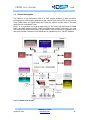
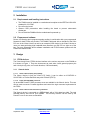
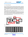
FM489 user manual V2.2 FM489 User Manual 4DSP Inc, 955 S Virginia Street, Suite 214, Reno, NV 89502, USA 4DSP bv, Crown Business Centre, Leidse Schouw 2, 2408 AE Alphen a/d Rijn, Netherlands Email: [email protected] This document is the property of 4DSP Inc. and may not be copied nor communicated to a third party without the written permission of 4DSP Inc. © 4DSP 2008 FM489 user manual V2.2 Revision History Date Revision Version March 5, 2008 First release 1.0 April 10, 2008 Major updates 1.1 Updated the DDR2 sdram size to be maximum 256MB Updated the JTAG pin locations Updated the DIP switch 1.2 Updated the Pn4 table 2.0 Apr 29, 2009 Added the technical support chapter and the external power warning 2.1 Sept 8, 2009 Modified QTE connector pinout table 2.2 February 18, 2009 March 3, 2009 September 2009 FM489 User manual www.4dsp.com -2- FM489 user manual V2.2 Table of Contents 1 Acronyms and related documents ............................................................................. 4 1.1 Acronyms............................................................................................................... 4 1.2 Related Documents ............................................................................................... 4 1.3 General description................................................................................................ 5 2 Installation ................................................................................................................... 6 2.1 Requirements and handling instructions ................................................................ 6 2.2 Firmware and software........................................................................................... 6 3 Design .......................................................................................................................... 6 3.1 FPGA devices ........................................................................................................ 6 3.1.1 Virtex-4 device ............................................................................................... 6 3.1.2 Virtex-5 device ............................................................................................... 9 3.2 FPGA devices configuration..................................................................................10 3.2.1 Flash storage ................................................................................................10 3.2.2 CPLD device .................................................................................................10 3.2.3 JTAG.............................................................................................................12 3.3 Clock tree..............................................................................................................13 3.4 Memory resources ................................................................................................14 3.4.1 BLAST QDR2 SRAM.....................................................................................14 3.4.2 BLAST DDR2 SDRAM ..................................................................................14 3.4.3 BLAST DDR3 SDRAM ..................................................................................14 3.4.4 DDR2 SDRAM ..............................................................................................14 3.5 Front Panel IO daughter card................................................................................15 3.5.1 Virtex-5 device to I/O front Panel daughter card ............................................15 3.5.2 Power connection to the front panel I/O daughter card..................................18 3.6 Front Panel Rocket IO...........................................................................................19 4 Power requirements ...................................................................................................20 4.1 External power connector for stand alone mode ...................................................21 5 Environment................................................................................................................23 5.1 Temperature .........................................................................................................23 5.2 Convection cooling................................................................................................23 5.3 Conduction cooling ...............................................................................................23 6 Safety...........................................................................................................................23 7 EMC .............................................................................................................................23 8 Technical support.......................................................................................................24 9 PCB revisions .............................................................................................................24 10 Warranty ..................................................................................................................25 September 2009 FM489 User manual www.4dsp.com -3- FM489 user manual V2.2 1 Acronyms and related documents 1.1 Acronyms ADC DAC DCI DDR DSP EPROM FBGA FPDP FPGA JTAG LED LVTTL LVDS LSB LVDS MGT MSB PCB PCI PCI-e PLL PMC QDR SDRAM SRAM Analog to Digital Converter Digital to Analog Converter Digitally Controlled Impedance Double Data Rate Digital Signal Processing Erasable Programmable Read-Only Memory Fineline Ball Grid Array Front Panel Data Port Field Programmable Gate Array Join Test Action Group Light Emitting Diode Low Voltage Transistor Logic level Low Differential Data Signaling Least Significant Bit(s) Low Voltage Differential Signaling Multi-Gigabit Transceiver Most Significant Bit(s) Printed Circuit Board Peripheral Component Interconnect PCI Express Phase Locked Loop PCI Mezzanine Card Quadruple Data rate Synchronous Dynamic Random Access memory Synchronous Random Access memory Table 1: Glossary 1.2 Related Documents IEEE Std 1386.1-2001: IEEE Standard Physical and Environmental Layers for PCI Mezzanine Cards (PMC). ANSI/VITA 39-2003: PCI-X for PMC and Processor PMC. ANSI/VITA 20-2001 : Conduction Cooled PMC. ANSI/VITA 42.0-2005: XMC Switched Mezzanine Card Auxiliary Standard. IEEE Std 1386-2001: IEEE Standard for a Common Mezzanine Card (CMC) Family. Xilinx Virtex-4 user guides Xilinx Virtex-5 user guides Xilinx PCI-X core datasheet September 2009 FM489 User manual www.4dsp.com -4- FM489 user manual 1.3 V2.2 General description The FM489 is a high performance PMC-X or XMC module dedicated to data acquisition, processing and communication applications with complex requirements. Built on the success of the FM48x series, the FM489 offers two FPGAs: the Virtex-4 and the Virtex-5. The latter has direct links to the BLAST sites. BLAST is an innovative and modular technology for the newer high performance FM489 PMC-X and XMC modules. BLAST, Board Level Advanced Scalable Technology, is a small PCB module that allows customization of the FM489 in memory extensions, processing units and communication interfaces. Each FM489 can be populated by up to 3 BLAST modules. . Figure 1: FM489 block diagram September 2009 FM489 User manual www.4dsp.com -5- FM489 user manual V2.2 2 Installation 2.1 Requirements and handling instructions The FM489 must be installed on a motherboard compliant to the IEEE Std 1386-2001 standard for 3.3V PMC Do not flex the board Observe SSD precautions when handling the board to prevent electrostatic discharges. Do not install the FM489 while the motherboard is powered up. 2.2 Firmware and software Drivers, API libraries and a program example working in combination with a pre-programmed firmware for both FPGAs are provided. The FM489 is delivered with an interface to the Xilinx PCI core in the Virtex-4 device as well as an example VHDL design in the Virtex-5 device so users can start performing high bandwidth data transfers over the PCI bus right out of the box. For more information about software installation and FPGA firmware, please refer the FM489 Get Started Guide. 3 Design 3.1 FPGA devices The Virtex-4 and Virtex-5 FPGA devices interface to the various resources on the FM489 as it is shown on Figure 1. They also interconnect to each other via 68 general purpose pins and 4 clock pins (2 pairs, one in each direction, 100Ω terminated). 3.1.1 3.1.1.1 Virtex-4 device Virtex-4 device family and package The Virtex-4 device is from the Virtex-4 FX family. It can be either an XC4VFX20 or XC4VFX60 in a Fineline Ball Grid array with 672 balls (FF672). 3.1.1.2 Power PC embedded processor Up to two IBM PowerPC RISC processor cores are available in the Virtex-4 device. This core can be used to execute C based algorithms and control the logic resources implemented in the FPGA. 3.1.1.3 Virtex-4 device external memory interfaces The Virtex-4 device is connected to a SDRAM bank with a 32-bit data bus width. The total SDRAM memory size can be up-to 256MB. This memory resource can be used by the PowerPC core or can serve as data buffer. September 2009 FM489 User manual www.4dsp.com -6- FM489 user manual 3.1.1.4 V2.2 PCI interface The Virtex-4 device interfaces directly to the PCI bus via the PMC Pn1, Pn2 and Pn3 connectors. An embedded PCI core from Xilinx is used to communicate over the PCI bus with the host system on the motherboard. PCI-X 64-bit 66MHz/133MHz, PCI 64-bit 66MHz and PCI 32-bit 33MHz are supported on the FM489. The bus type must be communicated at the time of the order so the right Virtex-4 device firmware can be loaded into the flash prior to delivery. The following performances have been recorded with the FM489 transferring data on the bus: PCI-X 64-bit 133MHz: 750Mbytes/s sustained PCI-X 64-bit 66MHz: 450Mbytes/s sustained PCI 32-bit 33MHz: 120Mbytes/s sustained 3.1.1.5 LED Four LEDs are connected to the Virtex-4 device. In the default FPGA firmware, the LEDs are driven by the Virtex-5 device via the inter-FPGA interface. The LEDs are located on side 2 of the PCB in the front panel area. Figure 2: FPGA LED locations September 2009 FM489 User manual www.4dsp.com -7- FM489 user manual 3.1.1.6 V2.2 Pn4 user I/O connector The Pn4 connector is connected to the Virtex-4 device. The 32 lower bits are available only if an XC4VFX60 device is mounted on board. All signals are single ended. 3.3V, 2.5V or 1.8V signalling can be chosen for Pn4. Connector pin 1 3 5 7 9 11 13 15 17 19 21 23 25 27 29 31 33 35 37 39 41 43 45 47 49 51 53 55 57 59 61 63 Signal name Pn4_IO0 Pn4_IO2 Pn4_IO4 Pn4_IO6 Pn4_IO8 Pn4_IO10 Pn4_IO12 Pn4_IO14 Pn4_IO16 Pn4_IO18 Pn4_IO20 Pn4_IO22 Pn4_IO24 Pn4_IO26 Pn4_IO28 Pn4_IO30 Pn4_IO32 Pn4_IO34 Pn4_IO36 Pn4_IO38 Pn4_IO40 Pn4_IO42 Pn4_IO44 Pn4_IO46 Pn4_IO48 Pn4_IO50 Pn4_IO52 Pn4_IO54 Pn4_IO56 Pn4_IO58 Pn4_IO60 Pn4_IO62 FPGA pin G16 G15 H13 H12 J16 H16 K13 J13 M11 N11 N8 N7 P11 P10 P8 R8 N21 M21 N18 N17 P21 P20 R18 P18 AA14 AA13 AB14 AC14 AD15 AD14 AE15 AF15 FPGA pin H14 G14 H11 J11 J15 J14 K12 K11 M10 M9 P6 N6 N9 P9 R7 R6 M20 M19 P16 N16 P19 N19 R17 R16 AB12 AA12 AC13 AC12 AE13 AD13 AF14 AF13 Signal name Pn4_IO1 Pn4_IO3 Pn4_IO5 Pn4_IO7 Pn4_IO9 Pn4_IO11 Pn4_IO13 Pn4_IO15 Pn4_IO17 Pn4_IO19 Pn4_IO21 Pn4_IO23 Pn4_IO25 Pn4_IO27 Pn4_IO29 Pn4_IO31 Pn4_IO33 Pn4_IO35 Pn4_IO37 Pn4_IO39 Pn4_IO41 Pn4_IO43 Pn4_IO45 Pn4_IO47 Pn4_IO49 Pn4_IO51 Pn4_IO53 Pn4_IO55 Pn4_IO57 Pn4_IO59 Pn4_IO61 Pn4_IO63 Connector pin 2 4 6 8 10 12 14 16 18 20 22 24 26 28 30 32 34 36 38 40 42 44 46 48 50 52 54 56 58 60 62 64 Table 2 : Pn4 pin assignment September 2009 FM489 User manual www.4dsp.com -8- FM489 user manual 3.1.2 3.1.2.1 V2.2 Virtex-5 device Virtex-5 device family and package The Virtex-5 device is dedicated to Digital Signal Processing applications and can be chosen from the SXT or LXT family devices. Its package is based on Fineline Ball Grid array with 1136 balls. In terms of logic and dedicated DSP resources, the FPGA B can be chosen from the following types: LT110T and SX95T. 3.1.2.2 Virtex-5 device BLAST interfaces BLAST, Board Level Advanced Scalable Technology, is a small PCB module that allows customization of the FM489 in memory extensions, processing units and communication interfaces. Each FM489 can be populated by up to 3 BLAST modules. BLAST modules available: • QDRII SRAM memory device: 1 x 2M x 32-bit (8MBytes) • DDR2 SDRAM memory device: 1 x 32M x 32-bit (128MBytes) • DDR3 SDRAM memory device: 2 x 64M x 16-bit (256MBytes) • ADV212 JPEG2000 compression devices: 2 CODECs • 8GB NAND Flash (Solid State Drive) 3.1.2.3 Virtex-5 device interface to Front Panel daughter card The Virtex-5 device interfaces to the front panel daughter card on the FM489 via a high speed connector. 174 I/Os are available from the FPGA to/from the daughter card. Refer to the Front Panel I/O section of this document for more details about the daughter card connector electrical characteristics. September 2009 FM489 User manual www.4dsp.com -9- FM489 user manual 3.2 V2.2 FPGA devices configuration 3.2.1 Flash storage The FPGA firmware is stored on board in a flash device. The 512Mbit device is partly used to store the configuration for both FPGAs. In the default CPLD firmware configuration, the Virtex-4 device A and the Virtex-5 device B are directly configured from flash if a valid bitstream is stored in the flash for each FPGA. The flash is preprogrammed in factory with the default firmware example for both FPGAs. Figure 3 : Configuration circuit 3.2.2 CPLD device As shown on Figure 2, a Cool Runner-II CPLD is present on board to interface between the flash device and the FPGA devices. The CPLD is used to program and read the flash. The data stored in the flash is transferred from the host motherboard via the PCI bus to the Virtex-4 device and then to the CPLD that writes the required bit stream to the storage device. A 31.25 MHz clock connects to the CPLD and is used to generate the configuration clock sent to the FPGA devices. At power up, if the CPLD detects that an FPGA configuration bitstream is stored in the flash for both FPGA devices, it will start programming the devices in SelecMap mode. Do NOT reprogram the CPLD without 4DSP’s approval The CPLD configuration is achieved by loading with a Xilinx download cable a bitstream from a host computer via the JTAG connector. The FPGA devices configuration can also be performed using the JTAG. September 2009 FM489 User manual www.4dsp.com - 10 - FM489 user manual 3.2.2.1 V2.2 DIP Switch A switch (J1) is located next to the JTAG programming connector (J6) see Figure 4. The switch positions are defined as follows: Figure 4: switch (J1) location Sw1 OFF Default setting. The Virtex-4 device configuration is loaded from the flash at power up. ON Virtex-4 device safety configuration loaded from the flash at power up. To be used only if the Virtex-4 device cannot be configured or does not perform properly with the switch in the OFF position. Sw2 Reserved Sw3 Reserved Sw4 Reserved Table 3: Switch description 3.2.2.2 LED and board status Four LEDs connect to the CPLD and give information about the board status. LED 0 LED 1 LED 2 September 2009 Flashing FPGA A or B bitstream or user_ROM_register is currently being written to the flash ON FPGA A not configured OFF FPGA A configured Flashing FPGA A or B bitstream or user_ROM_register is currently being written to the flash ON FPGA B not configured OFF FPGA B configured Flashing The Virtex-4 device has been configured with the safety configuration bitstream programmed in the flash at factory. Please write a valid Virtex-4 device bitstream to the flash. FM489 User manual www.4dsp.com - 11 - FM489 user manual LED 3 LED 3 V2.2 ON Flash is busy writing or erasing OFF Flash device is not busy ON CRC error. Presumably a wrong or corrupted FPGA bitstream has been written to the flash. Once on this LED remains on OFF No CRC error detected Table 4: LED board status Figure 5: CPLD LED locations 3.2.3 JTAG A JTAG connector is available on the FM489 for configuration purposes. The JTAG can also be used to debug the FPGA design with the Xilinx Chipscope. A press fit connector is delivered that can be plugged into the connector holes. The JTAG connector is located on side 1 of the PCB (see Figure 6). Figure 6: JTAG connector (J6) location September 2009 FM489 User manual www.4dsp.com - 12 - FM489 user manual V2.2 The JTAG connector pinout is as follows: Pin # 1 2 3 Signal 1.8V GND TCK Signal TMS TDI TDO Pin # 4 5 6 Table 5 : JTAG pin assignment 3.3 Clock tree The FM489 clock architecture offers an efficient distribution of low jitter clocks. Both FPGA devices receive a low jitter 125MHz clock. A low jitter programmable clock able to generate frequencies from 62.5MHz to 255.5MHz in steps of 0.5MHz is also available. This clock management approach ensures maximum flexibility to efficiently implement multiclock domains algorithms and use the memory devices at different frequencies. Both clock buffer devices (CDM1804) and the frequency synthesizer (ICS8430-61) are controlled by the Virtex-4 device. Two MGT reference clocks of 106.25MHz or 125MHz (Epson EG2121CA) are connected to the Virtex-5 device and make it possible to implement several standards over the MGT I/Os connected to the optical transceivers. Figure 7 : Clock tree September 2009 FM489 User manual www.4dsp.com - 13 - FM489 user manual 3.4 V2.2 Memory resources 3.4.1 BLAST QDR2 SRAM A maximum of 3 QDR2 SRAM devices can be connected to the virtex 5 device. This requires every BLAST site to be populated with a QDRII SRAM. The QDR2 SRAM device available on the FM489 is 2M words deep (9Mbytes, 2Mx36). 3.4.2 BLAST DDR2 SDRAM One 32Mx32-bit DDR2 SDRAM device (up to 128Mbytes) per BLAST site is possible. This will give the Virtex 5 device a maximum of 3 DDR2 banks with a total memory size of 756 MB 3.4.3 BLAST DDR3 SDRAM With the DDR3 SDRAM BLAST it is possible to have 6 ddr3 memory banks of 256 Mbytes that connect to the Virtex5 device. Each BLAST has two independent ddr3 memory banks. 3.4.4 DDR2 SDRAM One 64Mx32-bit DDR2 SDRAM device (up to 256Mbytes) is connected to the Virtex-4 FPGA device. This memory resource can be accessed by the PowerPC processor in the Virtex-4 device or can be used as a data buffer for custom user logic. Note: 256Mbytes of DDR2 SDRAM is available for the Virtex-4 FX60 only. September 2009 FM489 User manual www.4dsp.com - 14 - FM489 user manual 3.5 3.5.1 V2.2 Front Panel IO daughter card Virtex-5 device to I/O front Panel daughter card (Only available with daughter card purchase) The Virtex-5 device interfaces to a 180-pin connector placed in the Front panel I/O area (on both side 1 and side 2 of the PCB). It serves as a base for a daughter card and offers I/O diversity to the FM489 PMC. On side 2 of the PCB, the connectors and mounting holes placement complies with the SLB standard except for the 1.5V mounting hole that is not present on this module. The FPGA I/O banks are powered either by 1.8V, 2.5V or 3.3V via a large 0 ohms resistor (3.3V is the default if not specified otherwise at the time of order). Using the Xilinx DCI termination options to match the signals impedance allows many electrical standards to be supported by this interface. All signals are routed as 100Ω LVDS pairs and optionally 100Ω terminations can be fitted on the card. The VRP and VRN pins on the I/O banks connected to the daughter card connector are respectively pulled up and pulled down with 50Ω resistors in order to ensure optimal performances when using the Xilinx DCI options. The VREF pins are connected to 0.9V for DDR2 DCI terminations. Please, contact 4DSP Inc. for more information about the daughter card types available. The 180-pin Samtec connector pin assignment is as follows. All signals are shown as LVDS pairs in the table but they can be used for any standard that does not breach the electrical rules of the Xilinx I/O pad. Connector pin September 2009 Signal Name FPGA pin FPGA pin Signal name Connector pin 1 FP_P0 R6 3 FP_N0 T6 P7 FP_P1 2 P6 FP_N1 5 FP_X0 4 U10 T11 FP_X1 6 7 FP_P2 (2) T8 N5 FP_P3 8 9 FP_N2(2) U7 P5 FP_N3 10 11 FP_X2 T10 T9 FP_X3 12 13 FP_P4 N8 M6 FP_P5 14 15 FP_N4 N7 M5 FP_N5 16 17 FP_X4 R11 R8 FP_X5 18 19 FP_P6 M7 K7 FP_P7 20 21 FP_N6 L6 K6 FP_N7 22 23 FP_X6 R7 L4 FP_X7 24 25 FP_P8 H7 G6 FP_P9 26 27 FP_N8 J7 G7 FP_N9 28 29 FP_X8 D11 L16 FP_X9 30 31 FP_P10(2) J6 H5 FP_P11 32 33 FP_N10(2) J5 G5 FP_N11 34 35 FP_X10 K16 L15 FP_X11 36 37 FP_P12 F5 E6 FP_P13 38 39 FP_N12 F6 E7 FP_N13 40 41 FP_X12 L14 K14 FP_X13 42 43 FP_P14 N10 M10 FP_P15 44 45 FP_N14 N9 L9 FP_N15 46 47 FP_X14 K13 K12 FP_X15 48 49 FP_P16(2) K8 J14 FP_P17(1) 50 FM489 User manual www.4dsp.com - 15 - FM489 user manual 51 FP_N16(2) V2.2 K9 FP_N17(1) H13 52 53 FP_X16 J15 J12 FP_X17 54 55 FP_P18(1) H14 K11 FP_P19 56 57 FP_N18(1) H15 J11 FP_N19 58 59 FP_X18 H12 F14 FP_X19 60 Table 6 : Front Panel IO daughter card pin assignment Bank A (1) (2) Connected to a global clock pin on the FPGA. LVDS output not supported. Connected to a regional clock pin on the FPGA. LVDS output not supported. Connector pin Signal Name FPGA pin FPGA pin Signal name Connector pin 61 FP_P20 G11 H10 FP_P21 62 63 FP_N20 G12 H9 FP_N21 64 65 FP_X20 F15 E14 FP_X21 66 67 FP_P22 G8 F13 FP_P23 68 69 FP_N22 H8 G13 FP_N23 70 71 FP_X22 D14 F16 FP_X23 72 73 FP_P24(2) J10 F10 FP_P25 74 75 FP_N24(2) J9 G10 FP_N25 76 77 FP_X24 G17 J16 FP_X25 78 79 FP_P26 F9 E12 FP_P27 80 81 FP_N26 F8 E13 FP_N27 82 83 FP_X26 L19 C19 FP_X27 84 85 FP_P28 F11 E9 FP_P29 86 87 FP_N28 E11 E8 FP_N29 88 89 FP_X28 F18 M8 FP_X29 90 91 FP_P30 B13 D12 FP_P31 92 93 FP_N30 C13 C12 FP_N31 94 95 FP_X30 E19 G20 FP_X31 96 97 FP_P32 A13 A15 FP_P33 98 100 99 FP_N32 B12 A14 FP_N33 101 FP_X32 F20 L20 FP_X33 102 103 FP_P34 C14 E17 FP_P35(2) 104 105 FP_N34 C15 E16 FP_N35(2) 106 107 FP_X34 L21 K21 FP_X35 108 109 FP_P36(2) H17 H18 FP_N36(2) 110 111 3.3V/2.5V/1.8V Vbatt (3) 112 113 FP_X36 FP_X37 114 115 3.3V/2.5V/1.8V 0.9V 116 117 3.3V/2.5V/1.8V 3.3V/2.5V/1.8V 118 119 FP_X38 FP_X39 120 G22 K22 J22 G23 Table 7: Front Panel IO daughter card pin assignment Bank B (1) Connected to a global clock pin on the FPGA. LVDS output not supported. (2) Connected to a regional clock pin on the FPGA. LVDS output not supported. (3) Vbatt is connected to both Virtex-5 devices Vbatt pin. September 2009 FM489 User manual www.4dsp.com - 16 - FM489 user manual V2.2 Connector pin Signal Name FPGA pin FPGA pin Signal name Connector pin 121 FP_P37 B16 B17 FP_P38 122 123 FP_N37 B15 A16 FP_N38 124 125 FP_X40 H23 K23 FP_X41 126 127 FP_P39 C17 D16 FP_P40 128 129 FP_N39 D17 D15 FP_N40 130 131 FP_X42 E22 E23 FP_X43 132 133 FP_P41 D21 E21 FP_P42 134 135 FP_N41 D22 D20 FP_N42 136 137 FP_X44 F23 D24 FP_X45 138 139 FP_P43 F21 C20 FP_P44 140 141 FP_N43 G21 B20 FP_N44 142 143 FP_X46 E24 F24 FP_X47 144 145 FP_P45 (1) H19 B21 FP_P46 146 147 FP_N45(1) H20 A21 FP_N46 148 149 FP_X48 A29 B25 FP_X49 150 151 FP_P47 C22 A23 FP_P48 152 153 FP_N47 B22 A24 FP_N48 154 155 FP_X50 C25 C18 FP_X51 156 157 FP_P49 C23 C24 FP_P50 158 159 FP_N49 B23 D25 FP_N50 160 161 FP_X52 D29 A30 FP_X53 162 163 FP_P51 D26 B27 FP_P52 164 165 FP_N51 C27 A26 FP_N52 166 167 FP_X54 B30 C30 FP_X55 168 169 FP_P53(2) B26 C28 FP_P54 170 171 FP_N53(2) A25 D27 FP_N54 172 173 FP_X56 D30 A31 FP_X57 174 175 FP_P55(1) J20 A19 FP_P56 176 177 FP_N55(1) J21 A20 FP_N56 178 179 FP_X58 B31 D31 FP_X59 180 Table 8 : Front Panel IO daughter card pin assignment Bank C September 2009 FM489 User manual www.4dsp.com - 17 - FM489 user manual V2.2 3.5.2 Power connection to the front panel I/O daughter card The Front Panel I/O daughter card on side 1 of the PCB is powered via a 7-pin connector of type BKS (Samtec). Each pin can carry up to 1.5A. The power connector’s pin assignment is as follows. Pin # 1 3 5 7 Signal +3.3V +5V +12V -12V Signal +3.3V GND GND Pin # 2 4 6 Table 9: Daughter card power connector pin assignment on PMC side 1 On side 2 of the PCB, the daughter card is powered via a 33-pin connector of type BKS (Samtec). Each pin can carry up to 1.5A. The power connector’s pin assignment is as follows. Pin # 1 3 5 7 9 11 13 15 17 19 21 23 25 27 29 31 33 Signal +3.3V +3.3V +3.3V +3.3V +5V +5V +5V +5V +12V +12V -12V -12V GND Reserved Reserved Reserved GND Signal GND GND GND GND GND GND GND GND GND GND GND GND reserved reserved reserved reserved Pin # 2 4 6 8 10 12 14 16 18 20 22 24 26 28 30 32 Table 10: Daughter card power connector pin assignment on PMC side 2 September 2009 FM489 User manual www.4dsp.com - 18 - FM489 user manual 3.6 V2.2 Front Panel Rocket IO Eight Rx/Tx Multi Gigabit Transceivers connected to FPGA B are available in the front panel area on two connectors of type QTE. These connectors provide a base for a daughter card dedicated to high bandwidth communication via optical transceivers or copper (please refer to the FM489 web page for more details about available daughter cards). Infiniband protocols as well as Gigabit Ethernet, OC48 and Fibre channel (sFPDP) can be implemented over the transceivers. Eight LVTTL signals (four per connector) are also available for daughter card control. Two low jitter clocks (106.25MHz or 125MHz) are directly connected to the MGT clock inputs so multi-rate applications can be implemented on the FM489. The MGT banks have power supplies independent from the digital supply provided to the FPGAs in order to insure low noise and data integrity. LDO regulators are used to generate the 1V, 1.2V and 2.5V necessary for the MGT to operate. The power filtering network includes a 220nF decoupling capacitor and ferrite bead (MP21608S221A) per power pin. The signal differential pairs are routed on a specific inner layer with one reference GND plane on each side of the layer stack up. Figure 8: Multi Gigabit signals The table below provides the pinout for the two independent QTE connectors. Pin # 1 3 5 7 9 11 13 Signal Rx p3/7 Rx n3/7 Tx p3/7 Tx n3/7 Rx p2/6 Rx n2/6 Tx p2/6 Signal +3.3V +3.3V +3.3V +3.3V CTRL0/4 CTRL1/5 CTRL2/6 Pin # 2 4 6 8 10 12 14 Pin # 15 17 19 21 23 25 27 Signal Tx n2/6 Rx p1/5 Rx n1/5 Tx p1/5 Tx n1/5 Rx n0/4 Rx p0/4 Signal CTRL3/7 GND GND GND GND Tx n0/4 Tx p0/4 Pin # 16 18 20 22 24 26 28 Table 11: QTE connector pinout September 2009 FM489 User manual www.4dsp.com - 19 - FM489 user manual V2.2 4 Power requirements The Power is supplied to the FM489 via the PMC or XMC. Several DC-DC converters generate the appropriate voltage rails for the different devices and interfaces present on board. The FM489 power consumption depends mainly on the FPGA devices work load. By using high efficiency power converters, all care has been taken to ensure that power consumption will remain as low as possible for any given algorithm. After power up the FM489 typically consumes 2 Watts of power. For precise power measurements it is recommended to use the Xilinx power estimation tools for both the Virtex4 and Virtex-5 FPGA devices. The maximum current rating given in the table below is the maximum current that can be drawn from each voltage rail in the case resources are used to their maximum level. Device/Interface Voltage Maximum current rating 0.9V 5A Virtex-5 device core 1.0V 12A Virtex-4 device core 1.2V 12A QDR2, DDR2 SDRAM core and I/O banks, Virtex-4 devices I/O banks 1.8V 10A 1.8V/2.5/3.3V 1.5A 3.3V 2A Front Panel IO daughter card 5V 1A Front Panel IO daughter card 12V 0.5A Front Panel IO daughter card -12V 0.5A 1.2V, 1.5V, 2.5V 1.7A, 0.5A, 0.01A respectively DCI and voltage memory Virtex-5 device connected to the daughter card reference I/O front bank panel Virtex-4 device I/O bank connected to the PCI bus, Flash, CPLD, front Panel I/O daughter card MGT power supply Table 12 : Power supply Optionally, the FM489 can be used as a stand alone module and is powered via the external power connector. September 2009 FM489 User manual www.4dsp.com - 20 - FM489 user manual V2.2 Figure 9 : Power supply An ADT7411 device is used to monitor the power on the different voltage rails as well as the temperature. The ADT7411 data are constantly passed to the Virtex-4 device. Measurements can be accessed from the host computer via the PCI bus. A software utility delivered with the board allows the monitoring of the voltage on the 2.5V, 1.8V, 1.2V, 1.0V and 0.9V rails. It also displays both FPGAs junction temperature. 4.1 External power connector for stand alone mode An external power connector (J2) is available on side 2 of the PMC, next to the PMC connectors. It is used to power the board when it is in stand alone mode. This is a right angled connector and it will be mounted on board only if the card is ordered as a stand alone version (FM489-SA). The height and placement of this connector on the PCB breaches the PMC specifications and the module should not be used in an enclosed chassis compliant to PMC specifications if the external power connector is present on board. Do not connect an external power source to J2 if the board is powered via the PMC connectors. Doing so will result in damaging the board. The external power connector is of type Molex 43045-1021. Each circuit can carry a maximum current of 5A. The connector pin assignment is as follows: Pin # 1 3 5 7 9 Signal 3.3V 5V GND GND -12V Signal 3.3V 5V GND GND 12V Pin # 2 4 6 8 10 Table 13 : External power connector pin assignment September 2009 FM489 User manual www.4dsp.com - 21 - FM489 user manual V2.2 WARNING UNREGULATED UNPROTECTED EXTERNAL POWER SUPPLY CONNECTION This board is designed with an UNSUPPORTED feature for an external power connector labeled as J2. Mounting a connector on the PCB breaches the PMC electrical and mechanical specifications of the PMC standard. This is a FACTORY ONLY feature that is used in the manufacturing process when powering the board is required in an UNMOUNTED PCI bus mode, thus in stand alone mode. DO NOT connect an external power source to J2, doing so may result in damaging the board and will automatically VOID WARRANTY. Consult factory for further information. September 2009 FM489 User manual www.4dsp.com - 22 - FM489 user manual V2.2 5 Environment 5.1 Temperature Operating temperature 0°C to +60°C (Commercial) -40°C to +85°C (Industrial) Storage temperature: -40°C to +120°C 5.2 Convection cooling 600LFM minimum 5.3 Conduction cooling The FM489 can optionally be delivered as conduction cooled PMC. The FM489 is compliant to ANSI/VITA 20-2001 standard for conduction cooled PMC. 6 Safety This module presents no hazard to the user. 7 EMC This module is designed to operate from within an enclosed host system, which is build to provide EMC shielding. Operation within the EU EMC guidelines is not guaranteed unless it is installed within an adequate host system. This module is protected from damage by fast voltage transients originating from outside the host system which may be introduced through the system. September 2009 FM489 User manual www.4dsp.com - 23 - FM489 user manual V2.2 8 Technical support Technical support for all 4DSP Product, hardware, software and firmware is available under 4DSP Terms and Conditions of Sales ONLY in its original condition AS-SHIPPED unless agreed to by 4DSP and documented in writing, prior to any modifications. Terms and Conditions are available from http://www.4dsp.com/TCs.txt Technical support requests should be sent to [email protected] Any electrical connections made to the board or other components shall be made only with approved connectors as specifically identified in the products official documentation. Any modification to hardware including but not limited to removing of components, soldering or other material changes to in part or in whole to the PCM and/or its components will immediately invalidate and make void any warranty or extended support if any. Further, and changes or modifications to software and/or firmware supplied with the Product, unless provided for in the Products official documentation, shall immediately invalidate and make void any warranty or extended support if any. 9 PCB revisions Below a summary of the main differences between the PCB revisions: V2 - MGT reference clocks are AC coupled - The XMC reference clock has moved to balls AF3 and AF4 - Added protection circuitry to prevent damage in 12V XMC main boards V3 - - Modified the frontpanel IO area to support 4 optical transceivers. To do this the MGT connectors have been removed and the card is not compatible anymore to the conduction cooling specification. The BLAST site 0 and 1 have been remapped to be able to have the ddr3 signals compatible with the Xilinx MIG design. The XMC reference clock has been moved to balls Y3 and Y4 The MGT reference clock for the Optical tranceivers is mapped to balls D8 and C8 The XMC nMRSTI control signal has been connected to ball B18. The rest of the XMC control signals are disconnected. Modified the VPOWER protection circuitry September 2009 FM489 User manual www.4dsp.com - 24 - FM489 user manual V2.2 10 Warranty Hardware Software/Firmware Basic Warranty (included) 1 Year from Date of Shipment 90 Days from Date of Shipment Extended Warranty (optional) 2 Years from Date of Shipment 1 Year from Date of Shipment September 2009 FM489 User manual www.4dsp.com - 25 -