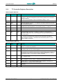
1
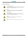
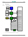
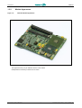
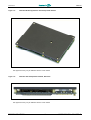
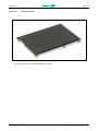
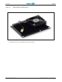
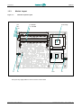
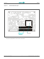
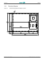
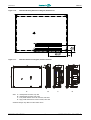
CPC1301 Pentium Core (2) Duo / Celeron M Based COM Express Module User Manual Rev. 001b E March 2010 The product described in this manual is compliant to all related CE standards. Product Title: Document Name: Document Version: Source doc. ver. CPC1301 CPC1301 User Manual 001b E 1.03, 1.06 Copyright © 2008, 2009, 2010 Fastwel Co. Ltd. All rights reserved. Revision Record Rev. Index Brief Description Product Index Date 001 Initial version CPC1301 October 2008 001a Reassertion of data; I C Controller and W atchdog Timer sections replaced CPC1301 April 2009 001b Processors list changes; temp. ranges correction; PCI-E x16 options; scattered minor corrections CPC1301 March 2010 2 Contact Information Fastwel Co. Ltd Fastwel Corporation US Address: 108 Profsoyuznaya st., Moscow 117437, Russian Federation 45 Main Street, Suite 319 Brooklyn, New York 11201 USA Tel.: +7 (495) 232-1681 +1 (718) 554-3686 Fax: +7 (495) 232-1654 +1 (718) 797-0600 Toll free: E-mail: [email protected] Web: http://www.fastwel.com/ +1 (877) 787-8443 (1-877-RURUGGED) CPC1301 Table of Contents Table of Contents ..............................................................................................................................................1 List of Tables .....................................................................................................................................................2 List of Figures ....................................................................................................................................................2 Notation Conventions.........................................................................................................................................3 General Safety Precautions................................................................................................................................4 Unpacking, Inspection and Handling...................................................................................................................5 Three Year Warranty..........................................................................................................................................7 1 Introduction...................................................................................................................................... 8 1.1 1.2 1.3 1.4 1.5 2 Detailed Description .......................................................................................................................25 2.1 2.2 2.1 2.3 2.4 2.5 2.6 3 Overview ................................................................................................................................................8 CPC1301 Versions..................................................................................................................................9 CPC1301 Diagrams ..............................................................................................................................10 1.3.1 Block Diagram ......................................................................................................................11 1.3.2 Module Appearance..............................................................................................................12 1.3.3 Module Layout ......................................................................................................................16 1.3.4 Dimensions Diagrams ...........................................................................................................18 Technical Characteristics.......................................................................................................................20 1.4.1 Processor, Memory and Chipset............................................................................................20 1.4.2 Interfaces .............................................................................................................................21 1.4.3 Control and Monitoring..........................................................................................................23 1.4.4 General ................................................................................................................................23 1.4.5 Software...............................................................................................................................24 Delivery Checklist..................................................................................................................................24 Processor, Memory and Chipset ............................................................................................................25 2.1.1 Processors ...........................................................................................................................25 2.1.2 System Memory....................................................................................................................25 2.1.3 Chipset.................................................................................................................................26 I2C Controller Input/Output Ports............................................................................................................27 2.2.1 I2C Controller Registers Description.......................................................................................28 Watchdog Timer....................................................................................................................................31 2.2.2 WDT Controller I/O Registers ................................................................................................32 CPC1301 Connectors ...........................................................................................................................34 2.3.1 COM Express Connectors.....................................................................................................34 2.4.1 SODIMM Connectors ............................................................................................................38 2.4.2 Other Connectors and Jumpers.............................................................................................38 Local SMBus Devices ...........................................................................................................................39 Serial EEPROM ....................................................................................................................................39 LED Indicators ......................................................................................................................................39 Installation.......................................................................................................................................40 3.1 3.2 3.3 3.4 3.5 CP C1 3 0 1 Safety Regulations ................................................................................................................................40 System Design Variants ........................................................................................................................41 Connection of Peripheral Devices: KIB1280 ...........................................................................................42 Installation of the Module.......................................................................................................................43 Dismounting..........................................................................................................................................43 Us e r M a n u a l 1 © 2 0 1 0 F a s t w e l V e r . 0 0 1 b E CPC1301 4 Configuration ..................................................................................................................................44 5 Phoenix® BIOS Setup .....................................................................................................................45 6 Power Requirements.......................................................................................................................46 7 Appendices .....................................................................................................................................47 7.1 Supplementary Information....................................................................................................................47 7.1.1 Related Standards and Specifications....................................................................................47 7.1.2 Troubleshooting....................................................................................................................48 Useful Abbreviations, Acronyms and Short-cuts .....................................................................................49 7.2 List of Tables Table 2-1: Table 2-2: Table 2-3: Table 2-4: Table 2-5: Table 6-1: Table 6-2: Table 7-1: Table 7-2: Table 7-3: PCI Express x16 Interface: Available Configurations....................................................................26 I2C Controller Registers ..............................................................................................................27 COM Express Connectors Pinout................................................................................................34 SMBus Devices..........................................................................................................................39 LED Indicators............................................................................................................................39 DC Input Voltage Ranges and Limits...........................................................................................46 CPC1301 Maximum Consumption Current ..................................................................................46 Related Standards......................................................................................................................47 Related Specifications ................................................................................................................47 Troubleshooting .........................................................................................................................48 List of Figures Figure 1-1: Figure 1-2: Figure 1-3: Figure 1-4: Figure 1-5: Figure 1-6: Figure 1-7: Figure 1-8: Figure 1-9: Figure 1-10: Figure 1-11: Figure 2-1: Figure 2-2: Figure 2-3: Figure 3-1: Figure 4-1: Figure 4-2: CPC1301 Block Diagram ............................................................................................................11 CPC1301 Module Appearance....................................................................................................12 CPC1301 Module Appearance with Heatspreader Intalled ...........................................................13 CPC1301 with Heatspreader Installed, Side View........................................................................13 Heatspreader Plate.....................................................................................................................14 Ribbed Heatsink with Mounted Fan.............................................................................................15 CPC1301 Top Side Layout .........................................................................................................16 CPC1301 Bottom Side Layout ....................................................................................................17 CPC1301 Mounting Dimensions Diagram, Top View ...................................................................18 CPC1301 Mounting Dimensions Diagram, Bottom View...............................................................19 CPC1301 Dimensions Diagram, Heatsink Versions .....................................................................19 I2C Controller Operation Flowchart: Write Data Byte to EEPROM Atmel AT24C02........................30 COM Express Connectors ..........................................................................................................34 SODIMM Connectors..................................................................................................................38 KIB1280 Carrier Board Appearance ............................................................................................42 J1 Jumper Switch.......................................................................................................................44 J5 Jumper Switch.......................................................................................................................44 All information in this document is provided for reference only, with no warranty of its suitability for any specific purpose. This information has been thoroughly checked and is believed to be entirely reliable and consistent with the product that it describes. However, Fastwel accepts no responsibility for inaccuracies, omissions or their consequences, as well as liability arising from the use or application of any product or example described in this document. Fastwel Co. Ltd. reserves the rights to change, modify, and improve this document or the products described in it, at Fastwel's discretion without further notice. Software described in this document is provided on an “as is” basis without warranty. Fastwel assumes no liability for consequential or incidental damages originated by the use of this software. This document contains information, which is property of Fastwel Co. Ltd. It is not allowed to reproduce it or transmit by any means, to translate the document or to convert it to any electronic form in full or in parts without antecedent written approval of Fastwel Co. Ltd. or one of its officially authorized agents. Fastwel and Fastwel logo are trademarks owned by Fastwel Co. Ltd., Moscow, Russian Federation. Ethernet is a registered trademark of Xerox Corporation. IEEE is a registered trademark of the Institute of Electrical and Electronics Engineers Inc. Intel is a trademark of Intel Corporation. Pentium M and Celeron M are trademarks of Intel Corporation. Microsoft is a trademark of the Microsoft corporation. In addition, this document may include names, company logos and trademarks, which are registered trademarks and, therefore, are property of their respective owners. Fastwel welcomes suggestions, remarks and proposals regarding the form and the content of this Manual. CP C1 3 0 1 Us e r M a n u a l 2 © 2 0 1 0 F a s t w e l V e r . 0 0 1 b E CPC1301 Notation Conventions Warning, ESD Sensitive Device! This symbol draws your attention to the information related to electro static sensitivity of your product and its components. To keep product safety and operability it is necessary to handle it with care and follow the ESD safety directions. Warning! This sign marks warnings about hot surfaces. The surface of the heatsink and some components can get very hot during operation. Take due care when handling, avoid touching hot surfaces! Caution: Electric Shock! This symbol warns about danger of electrical shock (> 60 V) when touching products or parts of them. Failure to observe the indicated precautions and directions may expose your life to danger and may lead to damage to your product. Warning! Information marked by this symbol is essential for human and equipment safety. Read this information attentively, be watchful. Note... This symbol and title marks important information to be read attentively for your own benefit. CP C1 3 0 1 Us e r M a n u a l 3 © 2 0 1 0 F a s t w e l V e r . 0 0 1 b E CPC1301 General Safety Precautions This product was developed for fault-free operation. Its design provides conformance to all related safety requirements. However, the life of this product can be seriously shortened by improper handling and incorrect operation. That is why it is necessary to follow general safety and operational instructions below. Warning! All operations on this device must be carried out by sufficiently skilled personnel only. Warning! When handling this product, special care must be taken not to hit the heatsink (if installed) against another rigid object. Also, be careful not to drop the product, since this may cause damage to the heatsink, CPU or other sensitive components as well. Please, keep in mind that any physical damage to this product is not covered under warranty. Note: This product is guaranteed to operate within the published temperature ranges and relevant conditions. However, prolonged operation near the maximum temperature is not recommended by Fastwel or by electronic chip manufacturers due to thermal stress related failure mechanisms. These mechanisms are common to all silicon devices; they can reduce the MTBF of the product by increasing the failure probability. Prolonged operation at the lower limits of the temperature ranges has no limitations. Caution, Electric Shock! Before installing this product into a system and before installing other devices on it, always ensure that your mains power is switched off. Always disconnect external power supply cables during all handling and maintenance operations with this module to avoid serious danger of electrical shock. CP C1 3 0 1 Us e r M a n u a l 4 © 2 0 1 0 F a s t w e l V e r . 0 0 1 b E CPC1301 Unpacking, Inspection and Handling Please read the manual carefully before unpacking the module or mounting the device into your system. Keep in mind the following: ESD Sensitive Device! Electronic modules and their components are sensitive to static electricity. Even a non-perceptible by human being static discharge can be sufficient to destroy or degrade a component's operation! Therefore, all handling operations and inspections of this product must be performed with due care, in order to keep product integrity and operability: n Preferably, unpack or pack this product only at EOS/ESD safe workplaces. Otherwise, it is important to be electrically discharged before touching the product. This can be done by touching a metal part of your system case with your hand or tool. It is particularly important to observe anti-static precautions when setting jumpers or replacing components. n If the product contains batteries for RTC or memory back-up, ensure that the module is not placed on conductive surfaces, including anti-static mats or sponges. This can cause shortcircuit and result in damage to the battery and other components. Store this product in its protective packaging while it is not used for operational purposes. n Unpacking The product is carefully packed in an antistatic bag and in a carton box to protect it against possible damage and harmful influence during shipping. Unpack the product indoors only at a temperature not less than +15°C and relative humidity not more than 70%. Please note, that if the product was exposed to the temperatures below 0°С for a long time, it is necessary to keep it at normal conditions for at least 24 hours before unpacking. Do not keep the product close to a heat source. Following ESD precautions, carefully take the product out of the shipping carton box. Proper handling of the product is critical to ensure correct operation and long-term reliability. When unpacking the product, and whenever handling it thereafter, be sure to hold the module preferably by the front panel, card edges or ejector handles. Avoid touching the components and connectors. Retain all original packaging at least until the warranty period is over. You may need it for shipments or for storage of the product. Initial Inspection Although the product is carefully packaged, it is still possible that shipping damages may occur. Careful inspection of the shipping carton can reveal evidence of damage or rough handling. Should you notice that the package is damaged, please notify the shipping service and the manufacturer as soon as possible. Retain the damaged packing material for inspection. After unpacking the product, you should inspect it for visible damage that could have occurred during shipping or unpacking. If damage is observed (usually in the form of bent component leads or loose socketed components), contact Fastwel's official distributor from which you have purchased the product for additional instructions. Depending on the severity of the damage, the product may even need to be returned to the factory for repair. DO NOT apply power to the product if it has visible damage. Doing so may cause further, possibly irreparable damage, as well as result in a fire or electric shock hazard. If the product contains socketed components, they should be inspected to make sure they are seated fully in their sockets. CP C1 3 0 1 Us e r M a n u a l 5 © 2 0 1 0 F a s t w e l V e r . 0 0 1 b E CPC1301 Handling In performing all necessary installation and application operations, please follow only the instructions supplied by the present manual. In order to keep Fastwel’s warranty, you must not change or modify this product in any way, other than specifically approved by Fastwel or described in this manual. Technical characteristics of the systems in which this product is installed, such as operating temperature ranges and power supply parameters, should conform to the requirements stated by this document. Retain all the original packaging; you will need it to pack the product for shipping in warranty cases or for safe storage. Please, pack the product for transportation in the way it was packed by the supplier. When handling the product, please, remember that the module, its components and connectors require delicate care. Always keep in mind the ESD sensitivity of the product. CP C1 3 0 1 Us e r M a n u a l 6 © 2 0 1 0 F a s t w e l V e r . 0 0 1 b E CPC1301 Three Year Warranty Fastwel Co. Ltd. (Fastwel), warrants that its standard hardware products will be free from defects in materials and workmanship under normal use and service for the currently established warranty period. Fastwel’s only responsibility under this warranty is, at its option, to replace or repair any defective component part of such products free of charge. Fastwel neither assumes nor authorizes any other liability in connection with the sale, installation or use of its products. Fastwel shall have no liability for direct or consequential damages of any kind arising out of sale, delay in delivery, installation, or use of its products. If a product should fail through Fastwel's fault during the warranty period, it will be repaired free of charge. For out of warranty repairs, the customer will be invoiced for repair charges at current standard labor and materials rates. Warranty period for Fastwel products is 36 months since the date of purchase. The warranty set forth above does not extend to and shall not apply to: 1. Products, including software, which have been repaired or altered by other than Fastwel personnel, unless Buyer has properly altered or repaired the products in accordance with procedures previously approved in writing by Fastwel. 2. Products, which have been subject to power supply reversal, misuse, neglect, accident, or improper installation. Returning a product for repair 1. Apply to Fastwel company or to any of the Fastwel's official representatives for the Product Return Authorization. 2. Attach a failure inspection report with a product to be returned in the form, accepted by customer, with a description of the failure circumstances and symptoms. 3. Carefully package the product in the antistatic bag in which the product had been supplied. Failure to package in antistatic material will VOID all warranties. Then package the product in a safe container for shipping. 4. The customer pays for shipping the product to Fastwel or to an official Fastwel representative or dealer. CP C1 3 0 1 Us e r M a n u a l 7 © 2 0 1 0 F a s t w e l V e r . 0 0 1 b E Introduction 1 CPC1301 Introduction This document presents general information on CPC1301 processor module, the details of its proper and safe installation, configuration and operation. 1.1 Overview CPC1301 is a COM Express Type II CPU module that fully complies with PICMG COM Express standard. It is based on Intel® Core™ 2 Duo/Core Duo/Celeron M CPUs operating at frequencies of up to 1.66 GHz with 533/667 MHz front side bus and on Intel chipset comprising 945GM GMCH and ICH7M DH. Memory interface supports dual or single channel DDR2 SDRAM through two SODIMM sockets with total capacity of up to 4 GB. CPC1301 is intended for high performance embedded systems, terminals, industrial computers. The module is designed for use with carrier boards conforming to PICMG COM Express Module Base Specification rev.1.0 for CPU modules with pinout Type II, for example with Fastwel KIB1280 ATX-format development carrier board. Multimedia functions are supported by interfaces for CRT monitor, flat panels with dual LVDS interface and AC'97/HD 5.1 audio. External graphic adapters can be connected through x16 PCI Express interface. S-Video interface is also available. Gigabit Ethernet channel makes this board perfect for developing communication intensive applications CPC1301 storage subsystem supports two SATA and one IDE UltraATA/100 disk drives. CPC1301 supports S3 (Suspend to RAM) mode. Additional reliability of СРC1301 is provided by hardware monitoring, watchdog timers, and a set of system monitoring features. CPC1301 operates in industrial (–40°C to +85°C) or commercial (0°C to +70°C) temperature ranges depending on the version. Supported operating systems – Microsoft DOS v. 3.30 – 6.22, Fastwel DOS (MS-DOS compatible); Windows 2000, XP, XP Embedded; QNX v. 4.20, 6.0; Linux 2.6. CP C1 3 0 1 Us e r M a n u a l 8 © 2 0 1 0 F a s t w e l V e r . 0 0 1 b E Introduction CPC1301 1.2 CPC1301 Versions The board is offered in flexible configuration. Options include different processors, the size of supplied system memory, and other options described in this section. Customer can choose necessary configuration options using the following template: 1 – 1 2 – 3 – 4 \ 5 Basic product name: CPC1301 2 Integral part of the product code (configuration version): 01 3 ICH7M DH, five x1 PCIe or one x4 and one x1 PCIe Processor: CD1.66 C2D1.5 CS1.06 4 Operating temperature range: I C 5 CP C1 3 0 1 Core Duo LV L2400, 1.66 GHz, 2 MB L2, 667 MHz FSB Core 2 Duo Mobile L7400, 1.5 GHz, 4 MB L2, 667 MHz FSB Celeron M 423, 1.06 GHz, 1 MB L2, 533 MHz FSB Industrial range, -40…+85°C (with CS1.06 only) Commercial range, 0…+70°C Other options: DDR2 SODIMM memory modules: Code Supplied Memory \SC-SODIMM-DDR2 1024 C One F-SODIMM-DDR2 1024, 0°C…+70°C \SC-SODIMM-DDR2 1024 I One F-SODIMM-DDR2 1024, -40°C…+85°C \SC-SODIMM-DDR2 2048 C One F-SODIMM-DDR2 2048, 0°C…+70°C \SC-SODIMM-DDR2 2048 I One F-SODIMM-DDR2 2048, -40°C…+85°C \DC-SODIMM-DDR2 1024 C Two F-SODIMM-DDR2 512, 0°C…+70°C \DC-SODIMM-DDR2 1024 I Two F-SODIMM-DDR2 512, -40°C…+85°C \DC-SODIMM-DDR2 2048 C Two F-SODIMM-DDR2 1024, 0°C…+70°C \DC-SODIMM-DDR2 2048 I Two F-SODIMM-DDR2 1024, -40°C…+85°C \DC-SODIMM-DDR2 4096 C Two F-SODIMM-DDR2 2048, 0°C…+70°C \DC-SODIMM-DDR2 4096 I Two F-SODIMM-DDR2 2048, -40°C…+85°C Us e r M a n u a l 9 © 2 0 1 0 F a s t w e l V e r . 0 0 1 b E Introduction CPC1301 Heatspreader, heatsink and fan (preliminary information): Code Description \R Heatspreader (with CS1.06 only) \R3 Ribbed heatsink, no fan, ribs oriented lengthwise, OSX77 \R3F Ribbed heatsink, with fan, ribs oriented lengthwise, OSX77 \R4 Ribbed heatsink, no fan, ribs oriented widthwise, OSX77 \R4F Ribbed heatsink, with fan, ribs oriented widthwise, OSX77 \R5 Ribbed heatsink, no fan, ribs oriented lengthwise, OSX98 \R5F Ribbed heatsink, with fan, ribs oriented lengthwise, OSX98 \R6 Ribbed heatsink, no fan, ribs oriented widthwise, OSX98 \R6F Ribbed heatsink, with fan, ribs oriented widthwise, OSX98 Custom configurations are available upon request Example: CPC1301 – 01 – CD1.66 – C \SC-SODIMM-DDR2 1024 C \R1 COM Express processor module, Intel® 945GM, SVGA, PCIe x16, LVDS, SATA, Gigabit Ethernet Core Duo 1.66 GHz, 2 MB cache, 667 MHz FSB Commercial temperature range, 0…+70°C One DDR2 SODIMM memory module, 1024 MB, commercial range Ribbed heatsink, no fan, ribs oriented lengthwise, ThermaFlo 1.3 CPC1301 Diagrams The diagrams in this section give visual information about the CPC1301 board design, its appearance, connectors and components layout. The diagrams may not reflect insignificant differences between the CPC1301 versions and generations. 6 CP C1 3 0 1 Us e r M a n u a l 10 © 2 0 1 0 F a s t w e l V e r . 0 0 1 b E Introduction 1.3.1 CPC1301 Block Diagram Figure 1-1: CPC1301 Block Diagram Type 2 Connector Hardware Monitor Intel Core (2) Solo/Duo CK-410 & SS Clocking FSB 533/667 MHz SODIMM Socket 1 DDR2 DRAM 667 MHz Up to 2 GB S-Video VGA CRT Ch-A Ch-B 945GM GMCH PCI-Express x16 SODIMM Socket 2 DDR2 DRAM 667 MHz Up to 2 GB LVDS DMI x4 Interface PATA SATA Ports 1, 2 SPI Flash 8 Mbit ICH7M DH SPI USB Ports 1-8 LPC Bus FPGA I2C Bus I2C Bus AC Link AC Link 8Mbit 32-bit PCI Bus PCI-Express Bus 32-bit PCI Bus PCI-Express x1* PCI-Express x1* PCI-Express x1* PCI-Express x1* CPU Core VR PCI-Express x1 GMCH VR (*) CP C1 3 0 1 DDR VR Gigabit Ethernet1 Power Supply 82573V Gigabit Ethernet Four x1 PCI Express channels can be aggregated into one x4 channel. Us e r M a n u a l 11 © 2 0 1 0 F a s t w e l V e r . 0 0 1 b E Introduction 1.3.2 CPC1301 Module Appearance Figure 1-2: CPC1301 Module Appearance The appearance may vary for different versions of the module. Heatspreader and memory modules are not shown. CP C1 3 0 1 Us e r M a n u a l 12 © 2 0 1 0 F a s t w e l V e r . 0 0 1 b E Introduction CPC1301 Figure 1-3: CPC1301 Module Appearance with Heatspreader Intalled The appearance may vary for different versions of the module. Figure 1-4: CPC1301 with Heatspreader Installed, Side View The appearance may vary for different versions of the module. CP C1 3 0 1 Us e r M a n u a l 13 © 2 0 1 0 F a s t w e l V e r . 0 0 1 b E Introduction CPC1301 Figure 1-5: Heatspreader Plate The appearance may vary for different versions of the plate. CP C1 3 0 1 Us e r M a n u a l 14 © 2 0 1 0 F a s t w e l V e r . 0 0 1 b E Introduction CPC1301 Figure 1-6: Ribbed Heatsink with Mounted Fan The appearance may vary for different versions of the heatsink. CP C1 3 0 1 Us e r M a n u a l 15 © 2 0 1 0 F a s t w e l V e r . 0 0 1 b E Introduction CPC1301 1.3.3 Module Layout Figure 1-7: CPC1301 Top Side Layout HL3 HL2 HL1 J1 J2 SODIMM J3 SODIMM North Bridge J4 CPU J5 The layout may slightly differ for various versions of the module. CP C1 3 0 1 Us e r M a n u a l 16 © 2 0 1 0 F a s t w e l V e r . 0 0 1 b E Introduction CPC1301 Figure 1-8: CPC1301 Bottom Side Layout J6 J7 South Bridge The layout may slightly differ for various versions of the module. CP C1 3 0 1 Us e r M a n u a l 17 © 2 0 1 0 F a s t w e l V e r . 0 0 1 b E Introduction 1.3.4 CPC1301 Dimensions Diagrams Figure 1-9: CP C1 3 0 1 CPC1301 Mounting Dimensions Diagram, Top View Us e r M a n u a l 18 © 2 0 1 0 F a s t w e l V e r . 0 0 1 b E Introduction CPC1301 Figure 1-10: CPC1301 Mounting Dimensions Diagram, Bottom View Figure 1-11: CPC1301 Dimensions Diagram, Heatsink Versions A B C D Note: A – Heatspreader mounted, top view B – Heatspreader mounted, side view C – Low profile heatsink and a fan mounted, side view D – High profile heatsink and a fan mounted, side view Heatsinks design may differ from the shown above. CP C1 3 0 1 Us e r M a n u a l 19 © 2 0 1 0 F a s t w e l V e r . 0 0 1 b E Introduction CPC1301 1.4 Technical Characteristics 1.4.1 Processor, Memory and Chipset CPU Intel® Core™ 2 Duo Processor (L7400) n n n n Up to 1.5 GHz Up to 4 MB L2 on-die cache 667 MHz PSB Enhanced SpeedStep Intel® Core™ Duo Processor (L2400) n n n n Up to 1.66 GHz Up to 2 MB L2 on-die cache 667 MHz PSB Enhanced SpeedStep Intel® Celeron M 423 Processor n n n n Up to 1.06 GHz Up to 2 MB L2 on-die cache 533 MHz PSB Enhanced SpeedStep Memory Main memory: n n n n Up to 4 GB of DDR2 SDRAM memory in two SODIMM sockets Memory frequency: 667/533 MHz (up to PC5300) Dual channel support PC SPD compatible Flash memory: n 8 Mbit SPI flash memory for BIOS storage EEPROM memory: n 64 Kbit of nonvolatile memory on SMBus Chipset Intel® 82945GM Graphics and Memory Controller Hub (GMCH) n n n n n n n n n CP C1 3 0 1 Us e r Optimized for Intel® Core™ processors 32-bit host bus addressing 64-bit AGTL+ based PSB interface at 533/667 MHz DMI interface 64-bit System Memory interface, optimized for dual channel DDR2 SDRAM memory symmetric and asymmetric modes Integrated 2D/3D Graphics and H/W Motion Compensation Engines Integrated DAC, 400 MHz Intel® Graphics Media Accelerator 950 Intel® Stable Image Technology M a n u a l 20 © 2 0 1 0 F a s t w e l V e r . 0 0 1 b E Introduction CPC1301 Intel® I/O Controller Hub ICH7M DH n n n n n n n n n n n n n n n n n 1.4.2 PCI-Express base specification rev. 1.0a PCI Bus rev. 2.3 interface at 33 MHz Integrated Serial ATA host controller Integrated IDE controller Ultra ATA 33/66/100, BMIDE and PIO modes USB 2.0 host interface ACPI 3.0 compliant power management logic DMI interface Low Pin Count (LPC) interface SPI interface Intel HighDefinition Audio interface, AC’97 v. 2.3 support Additional timer Intel® Active Management Technology support Enhanced DMA controller High precision event timers Interrupt controller System Management Bus Firmware Hub (FWH) interface support via LPC bus Interfaces PCI Bus Interface Compliant with 2.3 Specification at 33 MHz n n n n n System master operation Up to 6 Bus Master devices Support for 32-bit addressing on PCI using DAC protocol Six available PCI REQ/GNT pairs 3.3/5.0 V compatible PCI Express Interface n n n Five x1 channels Four x1 channels can be aggregated into one x4 channel One x16 PCI Express interface for external graphics card connection. It is possible to connect x2, x4, x8 PCI Express devices along with integrated graphics controller with certain limitations. Please, apply to manufacturer for details. SMBus Interface n n SMBus 2.0 Specification support 2 Compatible with most two-wire components that are also I C compatible USB Interface n n n CP C1 3 0 1 Us e r Up to eight USB 2.0 channels UHCI and EHCI support Data transfer rate up to 480 Mb/s M a n u a l 21 © 2 0 1 0 F a s t w e l V e r . 0 0 1 b E Introduction CPC1301 LAN Interface n n n n n One 10/100/1000 Mb/s Gigabit Ethernet interface Intel 82573V PCI-E bus Ethernet controller Automatic mode recognition Automatic cabling configuration recognition Cabling requirement: Category 5, UTP, four (two)-pair cabling Video Interfaces n n n n Built-in Intel 2D/3D high performance Intel® Graphics Media Accelerator 950 Hardware Motion Compensation Engine for software MPEG2 and MPEG4 decoding Intel® Stable Image Technology Video memory up to 64 MB shared with system VGA CRT n n Resolutions of up to 2048 x 1536, 16 bit at 75 Hz refresh rate Integrated RAMDAC, 400 MHz LVDS TFT n n n Dual/single channel interface Resolutions of up to 1600 x 1200, 18 bpp Spread spectrum clocking 25-112 MHz single/dual channel S-video n n n Three integrated 10-bit DACS NTSC/PAL HDTV support – 480p/720p/1080i/1080p n n AC97 audio rev. 2.3 High Definition audio available Audio Low Pin Count (LPC) Interface n Super I/O Winbond W83627HF interfaces supported: PS/2 Keyboard+Mouse, 1xLPT, 1xFDD, 2xRS-232 Mass Storage EIDE Ultra ATA 100/66/33 n One channel Serial ATA interface n n Two channels Data transfer rates up to 150 MB/s GPIO Lines n n 4-bit I/O port GPI[3:0] and GPO[3:0] signals are used. Operation mode of GPO2 and GPO3 is selected in BIOS Setup utility (see details in Chapter 4, Configuration) I2C Interface n CP C1 3 0 1 Us e r Master mode at 100 kHz supported M a n u a l 22 © 2 0 1 0 F a s t w e l V e r . 0 0 1 b E Introduction 1.4.3 CPC1301 Control and Monitoring Thermal Management The processor is protected from overheating by: n n n Internal processor temperature control unit, which initiates CPU shut down Processor die temperature monitor Heat spreader or heatsink with fan System Parameters Monitoring LM87 hardware monitor is used for supervision of the critical system parameters: n n n n System parameters monitoring via I2C or SMBus (switched in BIOS Setup) Main power voltages monitoring (VccCore, +3.3V, +5V, +12V) Processor die temperature monitoring Board temperature under SODIMM modules monitoring n n n Standby power LED (green) System status indicator (red) SATA activity LED (yellow) LEDs Watchdog Timers n n Chipset watchdog timer FPGA based programmable timer Additional Features n 1.4.4 Support for USB keyboard without Super I/O on carrier board General Mechanical COM Express Basic form-factor Dimensions: 95 × 125 mm (see Figure 1-7 for details) Board weight: less than 0.600 kg ~0.150 kg (without heatsink/heatspreader and fan) (to be amended) Shock/Vibration: 50G / 2G Power Supply Power is supplied to the module through COM Express connectors Max 3.2 A @ 12 V; 1.0 A @ 5V_SBY; 6.0 μA in off state (VCC_RTC) See Chapter 6 for details on power supply requirements Temperature Ranges Operational: 0°C ... +70°C – commercial range -40°C ... +85°C – industrial range (with CS1.06 only) Storage: -55°C ... +95°C Humidity 5% to 95% RH, non-condensing CP C1 3 0 1 Us e r M a n u a l 23 © 2 0 1 0 F a s t w e l V e r . 0 0 1 b E Introduction CPC1301 Battery External 3.0 V lithium battery for RTC on carrier board. Use PANASONIC BR2032 or compatible MTBF Not less than 140000 hours The value is calculated according to: Telcordia Issue 1 model, Method I Case 3, for continuous operation at a surface location, at normal environmental conditions (Russian State Standard GOST 15150-69, "UHL4" climatic parameters) and at ambient temperature 30°С. 1.4.5 Software BIOS Flash memory based enhanced Phoenix® BIOS Operating Systems Microsoft DOS v. 3.30 – 6.22 Fastwel DOS (MS-DOS compatible); Windows 2000, XP, XP Embedded; QNX v. 4.20, 6.0 Linux 2.6 1.5 Delivery Checklist The CPC1301 supplied set includes: 1. 2. 3. 4. 5. 6. 7. CPC1301 module Heatspreader / Ribbed heatsink (depending on version) Optional cooling fan (depending on version) Set of screws and standoffs (depending on version) CD-ROM with documentation and service software Antistatic bag Consumer carton box Note: Keep the antistatic bag and the original package at least until the warranty period is over. It can be used for future storage or warranty shipments. CP C1 3 0 1 Us e r M a n u a l 24 © 2 0 1 0 F a s t w e l V e r . 0 0 1 b E Detailed Description CPC1301 2 Detailed Description 2.1 Processor, Memory and Chipset 2.1.1 Processors The CPC1301 module is based on the Intel® Core™ 2 Duo / Core™ Duo / Celeron M processors operating at frequencies of up to 1.66 GHz. These processors combine high performance and low power consumption. Its enhanced performance characteristics are provided by a newly designed processor core with an integrated 64 KB L1 (32 KB instruction cache and 32 KB write-back data cache) and 2048 KB shared L2 cache (4 MB for Core™ 2 Duo). These processors support Enhanced Intel SpeedStep® technology to control power consumption and processor die temperature by switching the processor core voltage and frequency between several modes without need to reset the system. Important performance features of the Intel® Core Duo/Celeron M 423 processors also include n n n n n n n n Level 2 cache memory with Advanced Transfer architecture Intel® Architecture with Dynamic Execution Data Prefetch Logic Streaming SIMD (SSE2, SSE3) extensions 533/667 MHz FSB Execute Disable Bit technology support Intel® Virtualization technology support Dynamic Cache Sizing Moreover, Intel® Core 2 Duo processors support: n n n 2.1.2 Intel® 64 Architecture 4 MB Level 2 cache shared between cores Supplemental Streaming SIMD Extensions 3 (SSSE3) System Memory The module has two 200-contact SODIMM sockets onboard for DDR2 SDRAM memory modules. Total capacity of PC5300 compliant memory can be up to 4 GB. Dual channel operation and PC SPD (Serial Presence Detect) Specification are supported. CP C1 3 0 1 Us e r M a n u a l 25 © 2 0 1 0 F a s t w e l V e r . 0 0 1 b E Detailed Description 2.1.3 CPC1301 Chipset The CPC1301 chipset consists of the following devices: n n n 82945GM Graphics and Memory Controller Hub (GMCH) with DMI (Direct Media Interface) bus support ICH7M DH I/O Controller Hub with DMI bus One 1 MB SPI-flash memory chip North Bridge The 82945GM Graphics and Memory Controller Hub (GMCH) in the 1466 μFCBGA package provides interfaces with the microprocessor, dual- or single-channel DDR2 SDRAM system memory and includes a high performance graphics accelerator (Intel® GMA 950) as well as a x16 PCI Express interface for connection of an external graphics card on carrier board, for connection of general purpose input/output devices(*), or for two SDVO channels of the integrated graphics controller. It also provides a DMI interface to the ICH. Table 2-1: PCI Express x16 Interface: Available Configurations Device PCI Express Link Width Integrated Graphics Controller SDVO Interface External graphics controller x1, x16 Disabled Disabled General pupose IO device(*) x1 Enabled Enabled General pupose IO device(*) x2, x4, x8 Enabled Disabled (*) With limitations. Please, apply to manufacturer for details The 945GM is optimized for the Intel® Core family of microprocessors. The chipset supports a PSB frequency of 533/667 MHz with AGTL+ signaling. It also supports 32-bit addressing for using up to 4 GB memory address space. The 945GM includes a system memory controller with a 64-bit interface. The chipset supports up to PC5300 dual or single channel DDR2 SDRAMs for use as system memory. When running in internal graphics mode, high performance video capabilities of the 945GM are supported by a 2D/3D graphics accelerator and H/W Motion Compensation engines for software MPEG2 decoding. The internal graphics controller allows connection of a standard CRT display, a LVDS TFT panel, and digital displays with DVI interface. South Bridge The ICH7M DH is a multifunctional I/O Controller Hub that provides interfaces to the PCI-Express and PCI buses and to a number of PC interfaces, such as UltraDMA 100/66/33, SATA, USB 2.0 host interface, LPC interface, SPI interface, and AC'97 or HD digital audio. The ICH communicates with the host controller directly via a dedicated DMI interface. CP C1 3 0 1 Us e r M a n u a l 26 © 2 0 1 0 F a s t w e l V e r . 0 0 1 b E Detailed Description CPC1301 I/O Controller Hub features are: n n n n n n n n n n n n n 2.2 PCI-Express Base Specification enhanced rev 1.0a PCI bus interface, rev. 2.3, up to 6 Bus Master devices ACPI Power Management logic support Bus Master EIDE controller UltraDMA 100/66/33 SATA interface, two channels USB controller supporting eight USB 2.0 ports DMI interface with 945GM Intel® Active Management Technology LPC interface SPI interface AC'97 2.3 and High Definition audio interface RTC controller Additional timer I2C Controller Input/Output Ports I2C controller realized in FPGA as a LPC bus device supports Master mode and 100 kHz transmission frequency. Its activation and IRQ selection is performed in BIOS Setup. The device is operated via the registers within I/O ports area. Base address in I/O area is set by BIOS. It is indicated within the “Help” screen region to the right of “I2C Controller / GPIO Port” menu item of BIOS Setup program. GPIO (BASE+3) register is used to read and write GPI[3:0], GPO[3:0] I/O signals, routed to COM Express connector. I2C Controller Registers Table 2-2: I/O Port Address Type Hard Reset Configuration Register Base+0 R/W 00h Status Register Base+1 R/W 00h Control Register Base+2 R/W 00h Data Register Base+3 R/W 0xh GPIO Register CP C1 3 0 1 Us e r M a n u a l 27 © 2 0 1 0 F a s t w e l V e r . 0 0 1 b E Detailed Description CPC1301 I2C Controller Registers Description 2.2.1 Status Register (Base+0) Bit Name Type Function 7 MCF R/W Transaction state indicator: Completed / In process. It is set to “1” after acknowledgement (ACK) and stop phases of the transaction (STOP Condition). To start the next transaction it has to be cleared by writing “1” here. 6 – 5 MBB R Bus Busy indicator. It is set to “1” on detection of START Condition and is reset to “0” on STOP Condition. 4 MAL R/W Bus Arbitration Lost indicator. It is set to “1”, if bus arbitration is lost during START/STOP/Transmit phases. It can be reset by writing “1” to this bit. 3 – Reserved 2 – Reserved 1 MIF R/W Interrupt indicator. It is set to “1”, if MCF=“1” or MAL=“1”. The interrupt is generated, if MIEN bit is set in Control Register. It should be reset by writing “1” to this bit position. 0 RXAK R Transaction acknowledgement indicator. It is set to “0” on ACK receipt; it is set to “1”, if ACK is not received. In the absence of the transmission transaction acknowledgement (RXAK=1), the MSTA bit is automatically reset to “0” and STOP Condition is enabled. Reserved Control Register (Base+1) Bit Name Type Function 7 MEN R/W Controller enable/disable. Writing “1” here enables I2C controller. Writing “0” resets I2C controller and disables it. 6 MIEN R/W Interrupt enable. Writing “1” here enables interrupt generation. The interrupt is generated, if MIF bit is set in Status Register. 5 MSTA R/W Start transaction. Writing “1” here enables START Condition and transmit/receive phase depending on MTX bit value. Writing “0” here enables STOP Condition. In the absence of the transmit transaction acknowledgement (RXAK=1), this bit is automatically reset to “0” and STOP Condition is enabled. 4 MTX R/W Transaction mode selection. Writing “1” enables transmission mode, “0” – reception mode. 3 TXAK R/W Receive transaction acknowledgement bit. Writing “0” here enables acknowledgement (ACK), writing “1” disables acknowledgement (NAK). 2 RSTA R/W Restart. Writing “1” here enables Repeated Start Condition. It is reset to “0” automatically on completion of the restart phase. 1 – Reserved 0 – Reserved CP C1 3 0 1 Us e r M a n u a l 28 © 2 0 1 0 F a s t w e l V e r . 0 0 1 b E Detailed Description CPC1301 Data Register (Base+2) Bit Name 7-0 Type Function R/W In transmit mode, data written into this register is transmitted to the I2C bus; in receive mode, this register contains the data received from the I 2C bus. GPIO Register (Base+3) Bit Name Type Function 7-4 GPO R/W GPO[3:0] output values. GPO2 and GPO3 signals have dual functionality. Operation modes are set in BIOS Setup. They are used either as output ports or as ALERT# and THERM# outlets of LM87 chip. 3-0 GPI R GPI[3:0] input values CP C1 3 0 1 Us e r M a n u a l 29 © 2 0 1 0 F a s t w e l V e r . 0 0 1 b E Detailed Description CPC1301 I2C Controller Operation Flowchart: Write Data Byte to EEPROM Atmel AT24C02 Figure 2-1: Begin Switch the controller on (MEN=1) Bus busy? (MBB=1) Yes No Acknowledgement received? (RXAK=0) No Yes Write I2C header to data register (EEPROM address [7:1] + Write [0]) Write EEPROM data byte to data register and continue write transaction (MCF=0) Transmission mode selection and transaction start (MTX=1, MSTA=1) Transaction completed? (MCF=1) No Yes Transaction completed? (MCF=1) No Yes No Acknowledgement received? (RXAK=0) No Yes Acknowledgement received? (RXAK=0) Yes Continue transaction (MCF=0) (Automatic STOP-state generation) Generate STOP-state (MSTA=0) and continue transaction (MCF=0). Write EEPROM address byte to data register and continue write transaction (MCF=0) Transaction completed? (MCF=1) Transaction completed? (MCF=1) No Yes Yes CP C1 3 0 1 Us e r No End M a n u a l 30 © 2 0 1 0 F a s t w e l V e r . 0 0 1 b E Detailed Description 2.1 CPC1301 Watchdog Timer The FPGA based watchdog timer operates as an LPC device. Its activation and IRQ selection is performed in BIOS Setup. The device is operated via the registers within I/O ports area. Base address in I/O area is set by BIOS. It is indicated within the “Help” screen region to the right of “Watchdog Timer (WDT)” menu item of BIOS Setup program. Watchdog timer includes 24-bit Timer Current Value Register, which is decremented at frequency of 32.768 kHz, and Timer Initial Value Register. It is possible to set the timeout period from 0 to 512 seconds with increments of 30.52 ms by changing the value in this register. On the first expiry of the timeout period the watchdog timer can invoke an interrupt or Reset on second expiry. By default, the watchdog timer is not active. The equation below can be used to calculate the timeout TWD in ms as a function of the decimal value in the Timer Initial Value Register (KWD): TWD [ms] = KWD * 106 / 215 For example, decimal value "1" of KWD (000001h) corresponds to the timeout of 30.52 ms, and KWD = 16777215 (FFFFFFh) – 512 seconds. It is possible to reset the counter to the initial value in one of the following ways: 1. Write any value to Timer Current Value Register 2. Write any value to 80h port. This mode is enabled in BIOS Setup and is available only if access cycles to 80h port are translated to LPC bus. TMF flag is set on the first timeout expiry, STF flag is set on the second. Procedure of the watchdog timer control via I/O registers: 1. Stop the watchdog countdown. 2. Write the timeout value to the Timer Initial Value Register. 3. Initialize the watchdog in one of the two possible ways, for example, by writing any value to the Timer Current Value Register. This leads to wrting of the value in Timer Initial Value Register to the Timer Current Value Register. 4. Start the countdown and, if needed, enable the automatic Reset of the module. 5. It is necessary to strobe the watchdog timer with the period less than the set timeout period (TWD) in one of the ways described above. If the watchdog timer is not reset during the first timeout period, the TMF flag is set the interrupt is generated (if enabled). If the watchdog timer is not reset during the next timeout period, the STF flag is set and the second interrupt is generated (or the module will reboot, if Reset is enabled). CP C1 3 0 1 Us e r M a n u a l 31 © 2 0 1 0 F a s t w e l V e r . 0 0 1 b E Detailed Description 2.2.2 CPC1301 WDT Controller I/O Registers Timer Current Value Register [23:0] Base+0h Bit Name Description 7:0 Timer_Current_Value[7:0] Write/Read: Bits 7:0 of the current timer value Bit Name Description 7:0 Timer_Current_Value[15:8] Write/Read: Bits 15:8 of the current timer value Bit Name Description 7:0 Timer_Current_Value[23:16] Write/Read: Bits 23:16 of the current timer value Base+1h Base+2h Timer Initial Value Register [23:0] Base+3h Bit Name Description 7:0 Timer_Initial_Value[7:0] Write/Read: Bits 7:0 of the initial timer value Bit Name Description 7:0 Timer_Initial_Value[15:8] Write/Read: Bits 15:8 of the initial timer value Bit Name Description 7:0 Timer_Initial_Value[23:16] Write/Read: Bits 23:16 of the initial timer value CP C1 3 0 1 Us e r Base+4h Base+5h M a n u a l 32 © 2 0 1 0 F a s t w e l V e r . 0 0 1 b E Detailed Description CPC1301 Status Register Base+6h Bit Name Description 7:3 – Reserved 2 STM Write/Read: Second timeout flag. It is set to “1”, if TMF=1. This flag invokes interrupt. If RSTE=1 (Reset enabled), the module is rebooted. Cleared by writing “1” into this bit. 1 – Reserved TMF Write/Read: Timeout flag. It is set to “1” on expiry of the timeout. This flag enables interrupt generation. Cleared by writing “1” into this bit or by writing to 80h port (if this mode is enabled). 0 Control Register Base+7h Bit Name Description 7:2 – Reserved 1 CNTE Write/Read: Writing “1” enables watchdog countdown. 0 RSTE Write/Read: Writing “1” enables Reset on timeout. CP C1 3 0 1 Us e r M a n u a l 33 © 2 0 1 0 F a s t w e l V e r . 0 0 1 b E Detailed Description CPC1301 2.3 CPC1301 Connectors 2.3.1 COM Express Connectors Figure 2-2: COM Express Connectors J6 J7 Standard COM Express connectors (J6 and J7) are used to route module’s interfaces to carrier board connectors. The following table presents pin designation for these connectors. Table 2-3: COM Express Connectors Pinout AB Connector (J7) ## Cont. Signal 1 2 3 4 5 6 7 8 9 10 11 12 13 14 15 16 17 18 19 20 21 22 23 24 25 26 27 28 29 30 31 32 33 34 A1 A2 A3 A4 A5 A6 A7 A8 A9 A10 A11 A12 A13 A14 A15 A16 A17 A18 A19 A20 A21 A22 A23 A24 A25 A26 A27 A28 A29 A30 A31 A32 A33 A34 GND_(FIXED) GBE0_MDI3GBE0_MDI3+ GBE0_LINK100# GBE0_LINK1000# GBE0_MDI2GBE0_MDI2+ GBE0_LINK# GBE0_MDI1GBE0_MDI1+ GND_(FIXED) GBE0_MDI0GBE0_MDI0+ GBE0_CTREF SUS_S3# SATA0_TX+ SATA0_TXSUS_S4# SATA0_RX+ SATA0_RXGND_(FIXED) SATA2_TX+ SATA2_TXSUS_S5# SATA2_RX+ SATA2_RXBATLOW# ATA_ACT# AC_SYNC AC_RST# GND_(FIXED) AC_BITCLK AC_SDOUT BIOS_DISABLE# CP C1 3 0 1 Us e r M a n u a l CD Connector (J6) Note Pull-up 10K to 3.3V STBY Pull-up 10K to 3.3V Pull-up 10K to 3.3V STBY 34 Cont. Signal Note C1 C2 C3 C4 C5 C6 C7 C8 C9 C10 C11 C12 C13 C14 C15 C16 C17 C18 C19 C20 C21 C22 C23 C24 C25 C26 C27 C28 C29 C30 C31 C32 C33 C34 GND_(FIXED) lDE_D7 IDE_D6 IDE_D3 IDE_D15 IDE_D8 IDE_D9 IDE_D2 IDE_D13 IDE_D1 GND_(FIXED) IDE_D14 IDE_IORDY IDE_IOR# PCI_PME# PCI_GNT2# PCI_REQ2# PCI_GNT1# PCI_REQ1# PCI_GNT0# GND_(FIXED) PCI_REQ0# PCI_RESET# PCI_AD0 PCI_AD2 PCI_AD4 PCI_AD6 PCI_AD8 PCI_AD10 PCI_AD12 GND_(FIXED) PCI_AD14 PCI_C/BE1# PCI_PERR# © 2 0 1 0 Pull-up 10K to 3.3V STBY Pull-up 10K to 3.3V STBY Pull-up 10K to 3.3V Pull-up 10K to 3.3V Pull-up 10K to 3.3V Pull-up 10K to 3.3V F a s t w e l V e r . 0 0 1 b E Detailed Description CPC1301 AB Connector (J7) ## Cont. Signal 35 36 37 38 39 40 41 42 43 44 45 46 47 48 49 50 51 52 53 54 55 56 57 58 59 60 61 62 63 64 65 66 67 68 69 70 71 72 73 74 75 76 77 78 79 80 81 82 83 84 85 86 87 88 89 90 91 A35 A36 A37 A38 A39 A40 A41 A42 A43 A44 A45 A46 A47 A48 A49 A50 A51 A52 A53 A54 A55 A56 A57 A58 A59 A60 A61 A62 A63 A64 A65 A66 A67 A68 A69 A70 A71 A72 A73 A74 A75 A76 A77 A78 A79 A80 A81 A82 A83 A84 A85 A86 A87 A88 A89 A90 A91 THRMTRIP# USB6USB6+ USB_6_7_OC# USB4USB4+ GND_(FIXED) USB2USB2+ USB_2_3_OC# USB0USB0+ VCC_RTC EXCD0_PERST# EXCD0_CPPE# LPC_SERIRQ GND_(FIXED) PCIE_TX5+ PCIE_TX5GPI0 PCIE_TX4+ PCIE_TX4GND PCIE_TX3+ PCIE_TX3GND_(FIXED) PCIE_TX2+ PCIE_TX2GPI1 PCIE_TX1+ PCIE_TX1GND GPI2 PCIE_TX0+ PCIE_TX0GND_(FIXED) LVDS_A0+ LVDS_A0LVDS_A1+ LVDS_A1LVDS_A2+ LVDS_A2VDS_VDD_EN LVDS_A3+ LVDS_A3GND_(FIXED) LVDS_A_CK+ LVDS_A_CKLVDS_I2C_CK LVDS_I2C_DAT GPI3 KBD_RST# KBD_A20GATE PCIE0_CK_REF+ PCIE0_CK_REFGND_(FIXED) RSVD CP C1 3 0 1 Us e r M a n u a l CD Connector (J6) Note Pull-up 10K to 3.3V STBY Pull-up 10K to 3.3V STBY Pull-up 10K to 3.3V STBY Not used Not used Pull-down 4K-34.5K to GND Pull-down 4K-34.5K to GND Pull-down 4K-34.5K to GND Not used Not used Pull-up 10K to 3.3V Pull-up 10K to 3.3V Pull-down 4K-34.5K to GND Pull-up 10K to 3.3V STBY Pull-up 10K to 3.3V STBY 35 Cont. Signal Note C35 C36 C37 C38 C39 C40 C41 C42 C43 C44 C45 C46 C47 C48 C49 C50 C51 C52 C53 C54 C55 C56 C57 C58 C59 C60 C61 C62 C63 C64 C65 C66 C67 C68 C69 C70 C71 C72 C73 C74 C75 C76 C77 C78 C79 C80 C81 C82 C83 C84 C85 C86 C87 C88 C89 C90 C91 PCI_LOCK# PCI_DEVSEL# PCI__IRDY# PCI_C/BE2# PCI_AD17 PCI_AD19 GND_(FIXED) PCI_AD21 PCI_AD23 PCI_C/BE3# PCI_AD25 PCI_AD27 PCI_AD29 PCI_AD31 PCI_IRQA# PCI_IRQB# GND_(FIXED) PEG_RX0+ PEG_RX0-_ TYPE0# PEG_RX1+ PEG_RX1TYPE1# PEG_RX2+ PEG_RX2GND_(FIXED) PEG_RX3+ PEG_RX3RSVD RSVD PEG_RX4+ PEG_RX4RSVD PEG_RX5+ PEG_RX5GND_(FIXED) PEG_RX6+ PEG_RX6SDVO_DATA PEG_RX7+ PEG_RX7GND RSVD PEG_RX8+ PEG_RX8GND_(FIXED) PEG_RX9+ PEG_RX9RSVD GND PEG_RX10+ PEG_RX10GND PEG_RX11+ PEG_RX11GND_(FIXED) PEG_RX12+ Pull-up 10K to 3.3V Pull-up 10K to 3.3V Pull-up 10K to 3.3V © 2 0 1 0 Pull-up 10K to 3.3V Pull-up 10K to 3.3V Not connected Not connected F a s t w e l V e r . 0 0 1 b E Detailed Description CPC1301 AB Connector (J7) ## Cont. Signal 92 93 94 95 96 97 98 99 100 101 102 103 104 105 106 107 108 109 110 111 112 113 114 115 116 117 118 119 120 121 122 123 124 125 126 127 128 129 130 131 132 133 134 135 136 137 138 139 140 141 142 143 144 145 146 147 148 A92 A93 A94 A95 A96 A97 A98 A99 A100 A101 A102 A103 A104 A105 A106 A107 A108 A109 A110 B1 B2 B3 B4 B5 B6 B7 B8 B9 B10 B11 B12 B13 B14 B15 B16 B17 B18 B19 B20 B21 B22 B23 B24 B25 B26 B27 B28 B29 B30 B31 B32 B33 B34 B35 B36 B37 B38 RSVD GPO0 RSVD RSVD GND VCC_12V VCC_12V VCC_12V GND_(FIXED) VCC_12V VCC_12V VCC_12V VCC_12V VCC_12V VCC_12V VCC_12V VCC_12V VCC_12V GND_(FIXED) GND_(FIXED) GBE0_ACT# LPC_FRAME LPC_AD0 LPC_AD1 LPC_AD2 LPC_AD3 LPC_DRQ0# LPC_DRQ1# LPC_CLK GND_(FIXED) PWRBTN# SMB_CK SMB_DAT SMB_ALERT# SATA1_TX+ SATA1_TXSUS_STAT# SATA1_RX+ SATA1_RXGND_(FIXED) SATA3_TX+ SATA3_TXPWR_OK SATA3_RX+ SATA3_RXWDT AC_SDIN2 AC_SDIN1 AC_SDIN0 GND_(FIXED) SPKR I2C_CK I2C_DAT THRM# USB7USB7+ USB_4_5_OC# CP C1 3 0 1 Us e r M a n u a l CD Connector (J6) Note Pull-up 2.2K to 3.3V STBY Pull-up 2.2K to 3.3V STBY Not used Not used Not used Not used Not used Not used Not used Not used Pull-up 2.2K to 3.3V STBY Pull-up 2.2K to 3.3V STBY Pull-up 10K to 3.3V Pull-up 10K to 3.3V STBY 36 Cont. Signal Note C92 C93 C94 C95 C96 C97 C98 C99 C100 C101 C102 C103 C104 C105 C106 C107 C108 C109 C110 D1 D2 D3 D4 D5 D6 D7 D8 D9 D10 D11 D12 D13 D14 D15 D16 D17 D18 D19 D20 D21 D22 D23 D24 D25 D26 D27 D28 D29 D30 D31 D32 D33 D34 D35 D36 D37 D38 PEG_RX12GND PEG_RX13+ PEG_RX13GND RSVD PEG_RX14+ PEG_RX14GND_(FIXED) PEG_RX15+ PEG_RX15GND VCC_12V VCC_12V VCC_12V VCC_12V VCC_12V VCC_12V GND_(FIXED) GND_(FIXED) IDE_D5 lDE_D10 IDE_D11 IDE_D12 DE_D4 IDE_D0 IDE_REQ IDE_IOW# IDE_ACK# GND_(FIXED) IDE_IRQ IDE_A0 IDE_A1 IDE_A2 IDE_CS1# IDE_CS3# IDE_RESET# PCI_GNT3# PCI_REQ3# GND_(FIXED) PCI_AD1 PCI_AD3 PCI_AD5 PCI_AD7 PCI_C/BE0# PCI_AD9 PCI_AD11 PCI_AD13 PCI_AD15 GND_(FIXED) PCI_PAR PCI_SERR# PCI_STOP# PCI_TRDY# PCI_FRAME# PCI_AD16 PCI_AD18 © 2 0 1 0 Pull-up 10K to 3.3V STBY Pull-down 100K Pull-up 10K to 3.3V Pull-up 10K Pull-up 10K Pull-up 10K Pull-up 10K F a s t w e l to 3.3V to 3.3V to 3.3V to 3.3V V e r . 0 0 1 b E Detailed Description CPC1301 AB Connector (J7) ## Cont. Signal 149 150 151 152 153 154 155 156 157 158 159 160 161 162 163 164 165 166 167 168 169 170 171 172 173 174 175 176 177 178 179 180 181 182 183 184 185 186 187 188 189 190 191 192 193 194 195 196 197 198 199 200 201 202 203 204 205 B39 B40 B41 B42 B43 B44 B45 B46 B47 B48 B49 B50 B51 B52 B53 B54 B55 B56 B57 B58 B59 B60 B61 B62 B63 B64 B65 B66 B67 B68 B69 B70 B71 B72 B73 B74 B75 B76 B77 B78 B79 B80 B81 B82 B83 B84 B85 B86 B87 B88 B89 B90 B91 B92 B93 B94 B95 USB5USB5+ GND_(FIXED) USB3USB3+ USB_0_1_OC# USB1USB1+ EXCD1_PERST# EXCD1_CPPE# SYS_RESET# CB_RESET# GND_(FIXED) PCIE_RX5+ PCIE_RX5GPO1 PCIE_RX4+ PCIE_RX4GPO2(*) PCIE_RX3+ PCIE_RX3GND_(FIXED) PCIE_RX2+ PCIE_RX2GPO3(*) PCIE_RX1_+ PCIE_RX1WAKE0# WAKE1# PCIE_RX0+ PCIE_RX0GND_(FIXED) LVDS_B0+ LVDS_B0LVDS_B1+ LVDS_B1LVDS_B2+ LVDS_B2LVDS_B3+ LVDS_B3LVDS_BKLT_EN GND_(FIXED) LVDS_B_CK+ LVDS_B_CKLVDS_BKLT_CTRL VCC_5V_SBY VCC_5V_SBY VCC_5V_SBY VCC_5V_SBY RSVD VGA_RED GND_(FIXED) VGA_GRN VGA_BLU VGA_HSYNC VGA_VSYNC VGA_I2C_CK CP C1 3 0 1 Us e r M a n u a l CD Connector (J6) Note Pull-up 10K to 3.3V STBY Pull-up 10K to 3.3V Pull-up 4.7K to 3.3V Not used Not used Or INT# / ALERT# (LM87) Or THERM# (LM87) Pull-up 10K to 3.3V STBY Pull-up 10K to 3.3V STBY Not used Not used Pull-up 2.7K to 5V 37 Cont. Signal Note D39 D40 D41 D42 D43 D44 D45 D46 D47 D48 D49 D50 D51 D52 D53 D54 D55 D56 D57 D58 D59 D60 D61 D62 D63 D64 D65 D66 D67 D68 D69 D70 D71 D72 D73 D74 D75 D76 D77 D78 D79 D80 D81 D82 D83 D84 D85 D86 D87 D88 D89 D90 D91 D92 D93 D94 D95 PCI_AD20 PCI_AD22 GND_(FIXED) PCI_AD24 PCI_AD26 PCI_AD28 PCI_AD30 PCI_IRQC# PCI_IRQD# PCI_CLKRUN# PCI_M66EN PCI_CLK GND_(FIXED) PEG_TX0+ PEG_TX0PEG_LANE_RV# PE3_TX1+ PEG_TX1TYPE2# PEG_TX2+ PEG_TX2GND_(FIXED) PEG_TX3+ PEG_TX3RSVD RSVD PEG_TX4+ PEG_TX4GND PEG_TX5+ PEG_TX5GND_(FIXED) PEG_TX6+ PEG_TX6SDVO_CLK PEG_TX7+ PEG_TX7GND IDE_CBLID# PEG_TX8+ PEG_TX8GND_(FIXED) PEG_TX9+ PEG_TX9RSVD GND PEG_TX10+ PEG_TX10GND PEG_TX11+ PEG_TX11GND_(FIXED) PEG_TX12+ PEG_TX12GND PEG_TX13+ PEG_TX13- © 2 0 1 0 Pull-up 10K to 3.3V Pull-up 10K to 3.3V Pull-up 10K to 3.3V STBY Not connected Pull-up 4.7K to 3.3V STBY Not connected Pull-down 10K F a s t w e l V e r . 0 0 1 b E Detailed Description CPC1301 AB Connector (J7) CD Connector (J6) ## Cont. Signal Note Cont. Signal 206 207 208 209 210 211 212 213 214 215 216 217 218 219 220 B96 B97 B98 B99 B100 B101 B102 B103 B104 B105 B106 B107 B108 B109 B110 VGA_I2C_DAT TV_DAC_A TV_DAC_B TV_DAC_C GND_(FIXED) VCC_12V VCC_12V VCC_12V VCC_12V VCC_12V VCC_12V VCC_12V VCC_12V VCC_12V GND_(FIXED) Pull-up 2.7K to 5V D96 D97 D98 D99 D100 D101 D102 D103 D104 D105 D106 D107 D108 D109 D110 GND PEG_ENABLE# PEG_TX14+ PEG_TX14GND_(FIXED) PEG_TX15+ PEG_TX15GND VCC_12V VCC_12V VCC_12V VCC_12V VCC_12V VCC_12V GND_(FIXED) Note (*) GPO2 and GPO3 mode is set in BIOS Setup. 2.4.1 SODIMM Connectors Memory modules are installed in standard 200-contact SODIMM sockets – J2 (h = 9.2 mm) and J3 (h = 5.2 mm). Figure 2-3: SODIMM Connectors J2 J3 Single memory module can be intalled into any socket. To achieve maximum performance in sinchronous dual channel mode, two memory modules should be of the same capacity. 2.4.2 Other Connectors and Jumpers J1 and J5 jumpers are used to control system settings. Please refer to Chapter 4 (Configuration) in this document. J4 connector is used for system programming by the manufacturer. CP C1 3 0 1 Us e r M a n u a l 38 © 2 0 1 0 F a s t w e l V e r . 0 0 1 b E Detailed Description 2.4 CPC1301 Local SMBus Devices CPC1301 incorporates a System Management Bus to access several system monitoring and control devices via a two-wire I2C™ bus interface. The following table presents functions and addresses of onboard SMBus devices. Table 2-4: SMBus Devices Address Device D2h CY28411 clock oscillator A0h J3 DDR2 SODIMM memory module A2h J2 DDR2 SODIMM memory module ACh AT24C64 SPD EEPROM chip 5Ch LM87 hardware monitor 2.5 Serial EEPROM SPD serial 64 Kbit EEPROM chip is installed on CPC1301 and connected to SMBus. 2.6 LED Indicators Three LED indicators are located on the top side of the module. Table 2-5: LED Indicators Name Function HL1 Standby power LED (green). It is on when standby power is supplied to the module. HL2 System status indicator (red). After power-up this LED blinks rapidly (~8 Hz), after BIOS is started it blinks slowly (~1 Hz) until INT 19h BIOS procedure is finished then is constantly on. This LED is used for system startup troubleshooting. HL3 SATA activity (yellow). It is on while SATA device is active. CP C1 3 0 1 Us e r M a n u a l 39 © 2 0 1 0 F a s t w e l V e r . 0 0 1 b E Installation 3 CPC1301 Installation The CPC1301 is easy to install. However, it is necessary to follow the procedures and safety regulations below to install the module correctly without damage to the hardware, or harm to personnel. For details on installation of an operating system, please refer to the relevant software documentation. 3.1 Safety Regulations The following safety regulations must be observed when installing or operating the CPC1301. Fastwel assumes no responsibility for any damage resulting from infringement of these rules. Warning! When handling or operating the module, special attention should be paid to heatspreader or heatsink, because they can get very hot during operation. Do not touch heatspreader or heatsink when installing or removing the module immediately after the operation. Moreover, the module should not be placed on any surface or in any kind of package until the module and its hot parts have cooled down to ambient temperature. Caution! Switch off the system power before installing the module. Failure to follow this requirement can damage the module or entire system. ESD Sensitive Equipment! This product comprises electrostatically sensitive components. Please follow the ESD safety instructions to ensure module's operability and reliability: n n Use grounding equipment, if working at an anti-static workbench. Otherwise, discharge yourself and the tools in use before touching the sensitive equipment. Try to avoid touching contacts, leads and components. Extra caution should be taken in cold and dry weather. CP C1 3 0 1 Us e r M a n u a l 40 © 2 0 1 0 F a s t w e l V e r . 0 0 1 b E Installation 3.2 CPC1301 System Design Variants CPC1301 is supplied with one of the optional heat sinking devices: heat-conducting plate (heatspreader), ribbed heatsinks, and combinations of ribbed heatsinks with cooling fan. The heatsink or the heat-conducting plate is installed on the processor side of CPC1301 using six screws and thermal compound. The heatspreader is used in system designs with conductive heat sinking, for example to a metal outer housing. Ribbed heatsinks are used in a system case, where centralized forced air cooling is available. An optional cooling fan can be installed on the ribbed heatsink to further intensify heat dissipation. Power is supplied to the fan from the system power supply unit (fan connector on a carrier board). CPC1301 is installed on a carrier board using six stanoffs. Mounting the module on a carrier board, observe correct orientation of the module and ensure the complete engagement of the connectors. TBA CP C1 3 0 1 Us e r M a n u a l 41 © 2 0 1 0 F a s t w e l V e r . 0 0 1 b E Installation 3.3 CPC1301 Connection of Peripheral Devices: KIB1280 External devices are connected to CPC1301 via a carrier board for COM Express Type II pinout processor modules. Fastwel offers KIB1280, which can serve as an ATX development carrier board for CPC1301. Figure 3-1: KIB1280 Carrier Board Appearance The appearance may vary for different versions of the board. KIB1280 carrier board provides access to the following interfaces and connectors: VGA (RP D-Sub connector), S-Video (RP), LVDS, Gigabit Ethernet 10/100/1000-BaseT (one RJ45 RP connector), one x16 PCI Express, three x1 PCI Express connectors, three PCI headers, six USB 2.0 (two Type A RP connectors, four channels via onboard IDC headers), IDE UltraATA, four standard SATA connectors (two of them reserved), CF Type I/II socket with IDE interface, two RS232 COM ports (RP COM1 and onboard COM2), LPT (RP D-Sub) and FDD (IDC) standard connectors, two PS/2 RP connectors, two ExpressCard™ slots, Audio line in/out, MIC (RP), HD (5+1 out) Audio Connector, IrDA, LPC interface, SMBus, PLCC, two fan connectors, control&signalling interfaces and LEDs, ATX power supply header. Please, the KIB1280 User Manual for details. RP = Rear Panel connector CP C1 3 0 1 Us e r M a n u a l 42 © 2 0 1 0 F a s t w e l V e r . 0 0 1 b E Installation CPC1301 3.4 Installation of the Module To install CPC1301, follow the instructions below. 1. Keep to the safety regulations of the Section 3.1 when performing the following operations. Warning! Failure to accomplish the following instruction may damage the module or result in incorrect system operation. 2. Ensure that the module configuration corresponds to the application requirements before installing. For information regarding the configuration of the CPC1301, refer to Chapter 4. For the installation of CPC1301 specific peripheral devices, and I/O devices refer to the appropriate sections in Chapter 3. 3. To install the CPC1301: 1. Make sure that no power is connected to the system. 2. Mount the module on a carrier board using all supplied screws. 3. For CPC1301 versions with a ribbed heatsink with cooling fan - Connect the fan power cable to a carrier board connector. Provide conditions for sufficient cooling air flow. The fan air flow should be directed towards the heatsink. 3. Connect the required external interfacing cables to the carrier board's connectors and make sure that the module and all connected cables are properly fixed. The CPC1301 is now ready for operation. Please, refer to appropriate software, application, and system manuals to get further instructions. 3.5 Dismounting To unmount the module from the carrier board do the following: 1. When performing the next actions, keep to safety regulations of the Section 3.1. Pay special attention to the temperature of the heatsink or heatspreader! 2. Ensure that the system power is switched off before proceeding. 3. Disconnect the fan power cable (for version with a fan). 4. Unscrew the retaining screws. Do not touch the heatsink, since it can get very hot during operation. 5. Dispose of the module at your discretion. The module should not be placed on any surface or in any form of package until the board and the heatsink have cooled down to room temperature. CP C1 3 0 1 Us e r M a n u a l 43 © 2 0 1 0 F a s t w e l V e r . 0 0 1 b E Configuration 4 CPC1301 Configuration The module has J1 and J5 jumper switches used to configure the system. Figure 4-1: J1 Jumper Switch 1 3 2 4 Figure 4-2: Pins 1 and 2 closed – CMOS Reset. Pins 3 and 4 open – five x1 PCI-E channels, pins 3 and 4 closed – one x4 and one x1 PCI-E channel. J5 Jumper Switch 1 Pins 1 and 2 closed – +5V_STBY voltage supplied via COM Express connector is used by the module. Pins 2 and 3 closed – +5V_STBY voltage is not used by the module. With BIOS Setup utility it is possible to adjust the watchdog timer timeout and set parameters for I2C controller. See sections 2.3 and 2.2 respectively for instructions. In BIOS Setup it is also possible to switch between SMBus and I2C buses to be used for system parameters monitoring. The same utility is used to set operation mode for GPO2 and GPO3 signals, which are used either as output ports or as ALERT# and THERM# outlets of LM87 chip. Warning! All actions should be performed when the power is disconnected. Failure to follow this requirement can damage the module! ESD Sensitive Equipment! This product comprises electrostatically sensitive components. Please follow the ESD safety instructions to ensure module's operability and reliability: n n CP C1 3 0 1 Us e r M a n u a l Use grounding equipment, if working at an anti-static workbench. Otherwise, discharge yourself and the tools in use before touching the sensitive equipment. Try to avoid touching contacts, leads and components. 44 © 2 0 1 0 F a s t w e l V e r . 0 0 1 b E Phoenix® BIOS Setup 5 CPC1301 Phoenix® BIOS Setup The Phoenix® BIOS in your COM Express module is an adapted version of a standard BIOS for IBM PC AT-compatible personal computers equipped with Intel®x86 and compatible processors. The BIOS provides low-level support for the central processing, memory, and I/O system units. With the help of BIOS Setup program, you can modify the BIOS configuration parameters and control the special features of your module. The Setup program is started by pressing the F2 key and offers a convenient menu interface to modify basic system configuration settings and switching between the subsystems operation modes. These settings are stored in a dedicated batterybacked memory, CMOS RAM, which keeps the information when the power is switched off. To get the on-line help about the details of BIOS Setup program operation, please apply to the screen tips and the integrated help system. CP C1 3 0 1 Us e r M a n u a l 45 © 2 0 1 0 F a s t w e l V e r . 0 0 1 b E Power Requirements 6 CPC1301 Power Requirements Absolute maximum input voltages presented in the table below must not be exceeded to guarantee that the CPC1301 is not damaged. The ranges for the input power voltages, within which the module is functional, are also presented. Table 6-1: DC Input Voltage Ranges and Limits Name Power Voltage, V Vcc_12V +12 Vcc_5V_SBY +5 5.25 4.75 to 5.25 5.0 to 5.25 Vcc_RTC +3 3.3 2.0 to 3.3 3.0 to 3.3 Table 6-2: CPC1301 Maximum Consumption Current Maximum Permitted Value, V Absolute Limits, V 14.0 11.4 Recommended Range, V to 12.6 12.0 to 12.6 Processor Vcc_12V, A Vcc_5V_SBY, A Vcc_RTC in Power-off State, μA Core 2 Duo 1.5 GHz, 667 MHz FSB 3.2 1.0 6.0 Core Duo 1.66 GHz, 667 MHz FSB 3.0 1.0 6.0 Celeron 1.06 GHz, 533 MHz FSB 2.1 1.0 6.0 Power supplies to be used with the CPC1301 should comply with these requirements. CP C1 3 0 1 Us e r M a n u a l 46 © 2 0 1 0 F a s t w e l V e r . 0 0 1 b E Appendices CPC1301 7 Appendices 7.1 Supplementary Information 7.1.1 Related Standards and Specifications The Fastwel’s CPC1301 module comply with the requirements of the following standards: Table 7-1: Related Standards Type Standard Test Parameters Temperature change IEC 68-2-14-84 -40°C to 80°C (industrial range) 0°C to 70°C (commercial range) at RH=80%, non-condencing CE: Emission EN50081-1 (TBA) – CE: Immission EN61000-6-2:2001 – CE: Electrical safety EN60950 – Mechanical dimensions IEEE 1101.10 – Vibration (sinusoidal) IEC60068-2-6-82; Fc 2 g / 10-500 Hz / 10 (acceleration / frequency range / test cycles per axis) Single shock IEC60068-2-27-87; Ea 50 g / 9 ms / 18 / 3 s (peak acceleration / shock duration / number of shocks / recovery time in seconds) Multiple shock IEC60068-2-29-87; Eb 25 g / 11 ms / 1000±10 / 1 s (peak acceleration / shock duration half sine / number of shocks / recovery time) Important... Some versions of the module may have the test results differing from the ones presented in the above table. For more information, please contact Fastwel’s official representatives. Information related to this product and its components can be found in the following specifications: Table 7-2: Related Specifications Product Specification COM Express module PICMG COM.0. COM Express Module Base Specification TBA CP C1 3 0 1 Us e r M a n u a l 47 © 2 0 1 0 F a s t w e l V e r . 0 0 1 b E Appendices 7.1.2 CPC1301 Troubleshooting In case the module does not start read this section carefully before calling to service center; the reason is not necessarily in hardware problem. Please, refer also to LED Indicators section in this document. Table 7-3: Troubleshooting Symptoms Reason Actions The module does not start, HL1 LED is off. +5 V standby voltage is not supplied to the module. Check if J5 jumper switch is set correctly: ● Set to the correct position, if it is not set at all. ● If it is set to position 1-2, check presence of +5VSTBY voltage supplied from the carrier board. ● If it is set to position 2-3, check presence of +12 V voltage supplied from the carrier board and PWR_OK signal at contact B24 of J7 connector. The module does not start, HL1 LED is on, HL2 LED is off. +12 V power voltage is absent Onboard power sources are defective Check presence of +12 V power voltage supplied from the carrier board, and PWR_OK signal at contact B24 of J7 connector. Apply to service center. Missing or broken FPGA firmware PCIRST# signal is active The module does not start, HL1 LED is on, HL2 LED is rapidly blinking (~8 Hz) BIOS is missing or damaged The module is damaged Check the correctness of BIOS selection at the carrier board (if there is choice). Check BIOS_DISABLE# signal at contact A34 of J7 connector. If this signal is active, the BIOS is loaded from LPC FWH installed at the carrier board. Start the module with the reserve BIOS, if this option is provided at the carrier board, and restore BIOS at the module. Apply to service center. The module does not start, HL1 LED is on, HL2 LED is slowly blinking (~1 Hz), and the module beeps. CP C1 3 0 1 Us e r BIOS execution did not reach OS loading via INT19h. BIOS is corrupt M a n u a l Diagnose BIOS loading process using POST using POST codes and beeps. If diagnostics and repair is not possible, apply to service center. Start the module with the reserve BIOS, if this option is provided at the carrier board, and restore BIOS at the module. 48 © 2 0 1 0 F a s t w e l V e r . 0 0 1 b E Appendices 7.2 CPC1301 Useful Abbreviations, Acronyms and Short-cuts Abbreviation Meaning BMC Baseboard Management Controller PM Peripheral Management Controller IPMI Intelligent Platform Management Interface IPMB Intelligent Platform Management Bus 2 I C™ Inter Integrated Circuit Two-thread serial protocol, used in SMB and IPMI KCS interface Keyboard Controller Style interface Interface for communication between control software and BMC, similar to a keyboard controller interface BT interface Block Transfer interface Block transfer interface for communication between control software and BMC DDR SDRAM Double Data Rate Synchronous Dynamic Random Access Memory SODIMM Small Outline Dual In-Line Memory Module ECC Error Correction Code Data error correction technology used in memory modules FWH Firmware Hub Nonvolatile memory chip, part of Intel chipset, used for main and reserve BIOS copies in CPC1301 GMCH Graphics and Memory Controller Hub USB Universal Serial Bus LPC Low Pin Count External devices communication interface SMB System Management Bus UART Universal Asynchronous Receiver-Transmitter UHCI Universal Host Controller Interface USB Host Controller Interface EHCI Enhanced Host Controller Interface (Universal Serial Bus specification) UTP Unshielded Twisted Pair CRT-display Cathode Ray Tube Display PMC PCI (Peripheral Component Interconnect) Mezzanine Card CMC Common Mezzanine Card LVDS Low Voltage Differential Signal Digital monitors communication specification RTC Real Time Clock BIOS Basic Input-Output System PC Personal Computer PICMG PCI Industrial Computer Manufacturers Group AHA Accelerated Hub Architecture GMCH and ICH communication bus specification AGP Accelerated Graphics Port AGTL Advanced Gunning Transceiver Logic PSB (Processor Side Bus) signal exchange specification SMBus System Management Bus EEPROM Electrically Erasable Programmable Read-Only Memory NAND Flash Not And (electronic logic gate) Flash memory specification SSD Solid State Disk PLCC Plastic Leaded Chip Carrier RAMDAC Random Access Memory Digital-to-Analog Converter CP C1 3 0 1 Us e r M a n u a l 49 © 2 0 1 0 F a s t w e l V e r . 0 0 1 b E Appendices CPC1301 Abbreviation Meaning DAC Digital-to-Analog Converter DVMT Dynamic Video Memory Technology TTL Transistor-Transistor Logic ECP/EPP Extended Capabilities Port / Enhanced Parallel Port Parallel port specifications FDD Floppy Disk Drive EIDE Enhanced Integrated Drive Electronics Mass storage devices interface DMA Direct Memory Access PIO Programmed Input/Output EIDE: Directly processor controlled data exchange Rear I/O Board Rear Input-Output Board Auxiliary interface board, which is connected to the cPCI backplane rear connectors PWM output Pulse-Width Modulation Cooling fan control technique ESD Electrostatically Sensitive Device Electrostatic Discharge ACPI Advanced Configuration and Power Interface POST Power On Self Test cPCI CompactPCI Industrial automation systems standard EOS Electrical Overstress MDI Media Dependent Interface Interface with connection type automatical detection CP C1 3 0 1 Us e r M a n u a l 50 © 2 0 1 0 F a s t w e l V e r . 0 0 1 b E