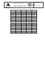
1
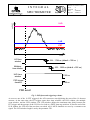
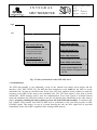
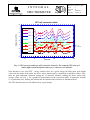
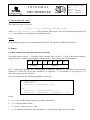
INTEGRAL
SPECTROMETER
SI I
ANNEX 8
PSD USER’S MANUAL
SPI-MU-0-1062V3-CNES
Issue
: 5
Revision : 0
Date
: 28/02/02
Page No. : ANX8-1
INTEGRAL
SPECTROMETER
SI I
SPI-MU-0-1062V3-CNES
Issue
: 5
Revision : 0
Date
: 28/02/02
Page No. : ANX8-2
PSD FM User Manual
SPI-MU-423-4215-CESR
Edition 2, Revision 0 (19/2/2001)
Author : J. Knödlseder
1. SCOPE OF THE DOCUMENT
The purpose of this document is to provide a user manual for the PSD FM subassembly. This manual
should introduce the user in the general functionality of the system, and should provide a reference
document that allows for a proper configuration and usage of the system.
2. REFERENCE DOCUMENTS
RD1
FM software version 227 / V1.07
RD2
PSD Software description, SPI-NT-4232-4194-CESR, Ed. 2, Rev. 0, 06/04/00
RD3
SPI INTERFACES SPECIFICATION, SPI-SI-0-1324-CNES, Issue 4, Rev. 0, 07/01/00
RD4
Spectrometer User Manual, SPI-MU-0-1062-CNES, Issue 4, Rev. 0, 10/11/00
3. GENERAL FUNCTIONALITY
The scope of this paragraph is the presentation of the general functionality of the PSD subassembly in
order to clarify the meaning of the PSD parameters.
3.1. Multiplexing
The PSD subassembly is equipped with 19 input channels (also called MUX channels), each connected to
one of the 19 fast detector output channels. Each of the 19 channels can be enabled or disabled
individually in order to activate or to suppress pulse-shape discrimination for individual detectors. A
disabled MUX channel neither generates FET triggers (see section 3.2), nor does it add to the sum of
detector currents provided to the A/D converters (see section 3.3).
Pulse Shape Discrimination for background reduction is only meaningful for events that are contained
within one germanium detector. Therefore it has been decided to have only one PSD system that treats all
19 detectors with an input multiplexing. If signals occur on several PSD inputs, the event is considered as
a multi-detector event and it will not be treated by the PSD sub-assembly (see section 3.2).
INTEGRAL
SPECTROMETER
SI I
SPI-MU-0-1062V3-CNES
Issue
: 5
Revision : 0
Date
: 28/02/02
Page No. : ANX8-3
3.2. Triggering
The PSD sub-assembly has its own triggering electronics that triggers the analysis of the Germanium
detector currents. The hardware trigger (or front-end trigger) is characterised by four parameters: the
FRONT END TRIGGER LEVEL (FET), the LOWER LEVEL DISCRIMINATOR (LLD), the
TIME WINDOW (TW), and the UPPER LEVEL DISCRIMINATOR (ULD). The first 3 quantities
(FET, LLD, TW) are configurable by telecommand while the ULD is a fixed level. The major aim of the
hardware threshold is to trigger the PSD system on detector pulses and to separate real event triggers from
noise triggers. Consequently, the optimum trigger parameters will depend on the noise in the system The
front-end trigger parameters are the most critical parameters of the PSD system since noise triggers can
easily exceed the expected event rates, leading directly to an exceed in time-tag rates sent to DFEE.
Each of the 19 input channels (MUX channels) has a front-end trigger threshold that is set by the FET
parameter. Note that the FET setting is common to all 19 detector channels, although the conversion
curve between trigger threshold and parameter setting is different for each of the 19 channels. This
implies that a given FET setting results in different FET threshold levels (see conversion table in section
4.2). The FET (or MUX) trigger defines the start of a PSD event (see Fig. 1).
The analogue signal of the 19 MUX channels is summed and distributed to the A/D converters (see
section 3.3) and the LLD and ULD threshold comparators. This means that the LLD and ULD levels are
common to all 19 channels, and possible variations in the threshold level among the 19 channels only
arise due to possible variations in the amplification gains of the pre-amplifiers of the 19 MUX channels.
INTEGRAL
SPECTROMETER
SI I
SPI-MU-0-1062V3-CNES
Issue
: 5
Revision : 0
Date
: 28/02/02
Page No. : ANX8-4
current
ULD
LLD
FET
time
LLD time
window
Multiples
time window
224 - 1784 ns (default = 392 ns )
432 - 1928 ns (default = 552 ns)
ULD time
window
1355 ns
PSD trigger
decision
1355 ns
PSD event
Fig. 1: PSD front-end triggering scheme.
As soon as one of the 19 FET triggered, the A/D converters start digitising the sum of the 19 detector
currents. At the same time, the FET trigger opens three time windows: the LLD window, the multiple
event window, and the ULD window. The LLD window defines the maximum time delay between the
FET trigger and the passage of the LLD level to lead to a DFEE time-tag emission. If after the end of the
LLD window the LLD level has not been exceeded, all 19 MUX channels are reset by a common reset
signal. The LLD window length is set by the parameter TW.
INTEGRAL
SPECTROMETER
SI I
SPI-MU-0-1062V3-CNES
Issue
: 5
Revision : 0
Date
: 28/02/02
Page No. : ANX8-5
The multiple event window defines the time window during which the occurrence of multiple FET
triggers will lead to a reset of the PSD front-end. If multiple FET fire during the multiple event window,
all 19 MUX channels will be reset by a common reset signal. This logic allows to eliminate multiple
detector hits since their analysis by the PSD is not scientifically meaningful. The multiple time window is
also set by the parameter TW, although the length of the multiple time window exceeds that of the LLD
window by typically 150 - 200 ns.
The ULD window defines the maximum time delay between the FET trigger and the passage of the ULD
level that may lead to a suppression of the DFEE time-tag. The goal of the ULD is the rejection of
saturated events that are not exploitable by the PSD (the ULD level in the FM corresponds to roughly
TBD keV). On the FM, the length of the ULD window has been adjusted to 1.355 µs. If a ULD trigger
occurred before the end of the ULD window a common reset signal will be sent to all 19 MUX channels.
Additionally, the MUX channels that have emitted a FET trigger since the start of the PSD event (i.e. the
first FET trigger) will be disabled for a time-period of TBD ns.
Once the ULD time window has passed, the PSD trigger decision is taken which decides if a DFEE timetag should be initiated. A DFEE time-tag will be initiated if at the start of the PSD trigger decision
window
• the LLD has triggered and
• only one FET trigger occurred and
• no ULD trigger occurred
In case that a time-tag has been initiated, an interrupt request will be issued to the PSD DSP (see
section 3.9). At the same time the A/D conversion of the germanium detector current is stopped. Still, a
Veto signal sent at the same moment by the DFEE to the PSD will inhibit time-tag emission, but the DSP
signal processing task will be started which first checks (by software) for the occurrence of a Veto signal.
In case of a Veto, the signal processing will be aborted immediately.
After signal processing by the PSD DSP the 19 MUX channels are reset by a common reset signal. Note
that if signal processing ends during the preparation of the HSL FIFO buffer (see section 3.7) the reset is
postponed until the FIFO buffer is filled to avoid interferences. This implies that during HSL FIFO
preparation, only one event is acceptable by the PSD.
3.3. Digitisation
After FET triggering, the sum of the 19 detector currents is digitised by 4 interleaved Analogue to Digital
converters at a frequency of 25 MHz, leading to a time resolution of 10 ns. The Analogue to Digital
converters have a resolution of 10 Bits, but only the 9 most significant Bits are used for the analysis
(leading to 512 digitisation units, ranging from 0 - 511). For the FM, the conversion function between
pulse voltage and digitisation units has been determined to
7.8 digits / mV
INTEGRAL
SPECTROMETER
SI I
SPI-MU-0-1062V3-CNES
Issue
: 5
Revision : 0
Date
: 28/02/02
Page No. : ANX8-6
With a typical PA2 gain of 18 mV / MeV1 , this converts into
140 digits / MeV
With a typical DC baseline of 45 digits, this corresponds to a maximum voltage of 60 mV for a
maximum digitisation value of 511 (corresponding to 3.3 MeV).
3.4. Veto
The PSD system may receive a Veto signal from the DFEE in order to suppress time-tag emission and
event processing. In the case that no DFEE cable is connected to the PSD, no veto is active, i.e. all events
are processed by the PSD.
The Veto signal is hardwired in the PSD and cannot be influenced by configuration commands.
3.5. Gain range
There are two gain ranges available in the PSD (low gain and high gain). Nominally, the PSD is operated
in high gain mode. The low gain mode reduces the gain by a factor of 2.2 with respect to the high gain
mode. For the FM, the gain ranges are
high gain : 200 keV - 3.3 MeV
low gain : 500 keV- 7.5 MeV
The gain range is common to all detectors and may be selected by configuration command. The FET
levels are not influenced by the gain range setting, while the LLD levels change.
3.6. Event identifier emission
The PSD system communicates with the DFEE subassembly by two signals:
1. A time-tag signal that is emitted if a trigger occurred in the PSD system
2. A data bus for identification of valid events (DFEE ID)
If a front-end trigger occurs in the PSD system without a Veto signal active, a time-tag is emitted to the
DFEE system. In the meanwhile, the PSD system has integrated the sum of the 19 germanium detector
currents using a 9 Bit hardware integrator in order to estimate the energy of the event. This energy
estimate is then compared to a validity range, specified for each detector individually by the LOWER
ENERGY THRESHOLD (LET) and the UPPER ENERGY THRESHOLD (UET). The LET and
UET are configurable for each detector by configuration commands. If the pulse integral falls within the
validity interval, an event identifier with processing flag P=1 is emitted to the DFEE. If the pulse falls
outside the energy interval, the processing flag in the DFEE label is set to P=0.
1
All energy values given in keV or MeV in this document are based on a conversion coefficient of 18 mV / MeV.
INTEGRAL
SPECTROMETER
SI I
SPI-MU-0-1062V3-CNES
Issue
: 5
Revision : 0
Date
: 28/02/02
Page No. : ANX8-7
The relation between the hardware integrator 9 Bit value and the energy is rather complex since the
integral is composed of both the pulse area and the baseline area and the sum of the 19 detector currents.
The baseline may vary as function of time and event frequency. The value of the hardware integrator is
inserted into the first bin of a PSD curve when downlinked by TM. This allows for the calibration of the
hardware integrator versus energy.
3.7. HSL
Scientific data is transmitted on the HSL from the PSD subassembly to the DPE subassembly. The
scientific data consists of:
1. event data
2. curve data
The maximum number of curves that are transmitted in a HSL data frame, and the frequency of curve
data transmission can be configured using configuration commands. The transmission rates may differ
between the operational mode and the calibration or diagnostic mode.
Detector pulses that were accumulated during cycle n of the 8 Hz HSL clock are sent to the DPE during
cycle n+1. A new cycle begins with the falling edge of the 8 Hz clock. At this moment the PSD
subassembly prepares the data frame in a FIFO buffer. It may happen that at the moment of the 8 Hz
falling edge not all events of cycle n are yet processed, hence they would be lost since they are not
allowed to be sent in cycle n+2. For this reason, a post processing of 10 events at maximum is allowed
after the falling edge of the 8 Hz clock occurs. Note that during this entire post-procession period, the
PSD may only accept one new event trigger at maximum. The FIFO buffer is only prepared after this
postprocessing. The maximum number of events to be postprocessed can be set by configuration
commands. Unprocessed events (due to a lack of processing time) will be dropped. The number of
dropped events is reported in TM.
3.8. Pulse shape discrimination
Pulse shape discrimination is performed by comparing measured detector pulse shapes to a library of
pulse shape templates. As result of the comparison, an event may be flagged as single site event (most
significant Bit of the PSD word set to 0) or as multiple site event (most significant Bit of the PSD word
set to 1). Event selection statistics are maintained in the housekeeping telemetry.
Library templates can be uploaded using telecommands for each individual detector. The libraries are
stored in EEPROM. Two library sets may be uploaded for each detector. The selection of the library set is
done via configuration command. Furthermore, the number of time-steps used for the pulse shape
analysis and the number of library templates are also configurable.
INTEGRAL
SPECTROMETER
SI I
SPI-MU-0-1062V3-CNES
Issue
: 5
Revision : 0
Date
: 28/02/02
Page No. : ANX8-8
3.9. DSP32 software
The PSD subassembly houses a DSP32C digital signal processor. This processor handles all
communications with the environment (LSL, HSL, DFEE) and performs the scientific analysis of the
digitised pulses shapes. The software in the PSD is composed of two parts:
1. The functional software (eng.s) that handles all interfaces and the data accumulation and preparation
2. The scientific software (science.s) that analyses the pulse shapes and handles the library
management
In the FM, the functional software has version number 230 and the scientific software has version number
V1.08.
After start-up, the PSD program code that resides in ROM is copied into RAM and code execution will
then be passed to RAM. The only exception is the software maintenance mode for which code execution
takes place in ROM (hence the entire RAM area is patchable). For more information about the memory
management, please refer to section 6.
The PSD code consists of a main program loop that handles (in the given order) in one loop
• one command of the LSL command buffer
• synchronous housekeeping update and HSL buffer transfer (see section 3.10)
• scientific analysis of one pulse shape in the pulse buffer (see RD1)
The LSL command buffer and the pulse buffer are filled by two interrupt routines. The routine with the
highest priority is the trigger of the front-end electronics which leads to the digitalisation of the current
pulse. At this level, the Veto signal is analysed and the pulse energy is estimated (see section 3.6). The
pulse is then put into a warp around pulse buffer of 40 kByte length and processing is passed back to the
main loop. Each pulse takes 256 Bytes in the buffer, allowing 160 pulses to be stored (buffered) at any
time.
LSL commands received from DPE also lead to an interrupt, but with lower priority than the pulse trigger
interrupt. The LSL interrupt routine checks the coherency of the LSL signal (checksum) and posts a LSL
response (ACK or NACK) in an LSL response warp around buffer of 768 Bytes length. The content of
this buffer is then sent to the DPE via the same interrupt routine. In case that the command was a memory
dump request, a housekeeping or status request, or a configuration read-back command, the data field of
the response (i.e. memory field or configuration field) is also added to the response buffer.
INTEGRAL
SPECTROMETER
SI I
SPI-MU-0-1062V3-CNES
Issue
: 5
Revision : 0
Date
: 28/02/02
Page No. : ANX8-9
The LSL command is then put into a command buffer for later treatment in the main program loop (for
dump, housekeeping or status request, or configuration read-back commands, no further treatment is
required; the only exception is the request of the HK 13 housekeeping block which resets the error Bit in
the status work). The LSL buffer is a warp around buffer of 768 Bytes length. Eventually, if too many
commands are sent, and the buffer length of 768 Bytes become exceeded, some old buffer content may be
overwritten, which is signalled by the Command Synchronisation Error Bit in HK 0 (note, however,
that the command synchronisation Bit has been erased from the SPI database since there is no method that
allows to reset the Bit).
The scientific software (science.s) performs the analysis of the measured pulse shapes using the
algorithm described in RD1. The number of pulse shapes that may be analysed by the PSD per second
depends mainly on the execution speed of the analysis algorithm, which has therefore been highly
optimised. In detail, the execution speed depends on the number of library templates that are used for the
analysis and the number of bins in the template that are considered (both parameters are configurable by
telecommand; see section 5.2). The following performances were determined for the FM code (typical
values are 64 bins and 30 templates, marked in bold):
Bins
Templates
Time (µs)
64
25
830
64
30
940
64
33
1000
64
38
1100
40
38
950
50
38
1020
3.10. Internal PSD synchronisation
Some tasks in the PSD sub-assembly, such as housekeeping data refresh and HSL data transfer, are
synchronised on the 8 Hz clock provided by the DPE. The synchronised task are summarised
schematically in Fig. 2. Within one 8 Hz cycle (125 ms cycle), some tasks are executed after the falling
clock edge, others are executed after the rising clock edge. The tasks listed in Fig. 2 are given in the order
of execution, i.e. the top-most task is executed first.
To allow also synchronisation on time-scales longer than 125 ms the PSD sub-assembly maintains an
internal 8 Hz clock counter (unsigned 16 Bit integer roll-over counter) which increments by one each
time the PSD detects a falling 8 Hz clock edge. Each time the counter increments, the corresponding field
in the TM buffer is updated immediately. At the same time, the last DFEE label that has been sent to the
DFEE is stored in the TM buffer.
INTEGRAL
SPECTROMETER
SI I
SPI-MU-0-1062V3-CNES
Issue
: 5
Revision : 0
Date
: 28/02/02
Page No. : ANX8-10
Before filling the HSL FIFO buffer for data transfer between PSD and DPE, a specified number of events
that may still remain in the curve input buffer of the PSD may be processed (see section 4.5). Any event
that remains in the buffer after pre-processing will not be transmitted by PSD to DPE, and will be
dropped.
Tasks after a rising 8 Hz clock edge are executed on several time-scales. Each clock, one of the 8 A/D
values in the TM, such as voltages (section 7.1.1) and temperatures (section 7.1.2), is read from the
analogue board and is immediately updated in the TM buffer. Since only one value is updated at a time a
total of eight 8 Hz clocks (or one second) is required before all values have been refreshed.
LLD and ULD rates (section 7.2.3) are read each second from the ACTEL chip. Each two seconds, the
rates are accumulated and stored in an internal buffer. Only each 64 seconds, the 32 two second rates are
transferred from this buffer into the TM buffer for downlink. A second is defined by the 3 least significant
Bits of the 8 Hz counter being 0. The two second intervals are defined by the Bit sequence 1000 for the
least 4 significant Bits of the 8 Hz counter. A 64 second interval starts with the 9 least significant Bits of
the 8 Hz counter being 0.
In addition to the LLD and ULD rates, the channel rates (section 7.2.1), the selection statistics (section
7.2.2), some control fields (section 7.2.5), and the number of dropped events (section 7.2.6), are updated
each 64 seconds in the TM transfer buffer. Note that the number of dropped events is a 16 Bit integer rollover counter which is reset to zero after transfer to the TM buffer.
INTEGRAL
SPECTROMETER
SI I
SPI-MU-0-1062V3-CNES
Issue
: 5
Revision : 0
Date
: 28/02/02
Page No. : ANX8-11
high
low
Each clock (125 ms):
- increment 8 Hz counter
- store last DFEE label for TM
- event post processing
- fill HSL FIFO buffer
Each 8th clock (1 s):
- update A/D control word
- update ACTEL control word
Each clock (125 ms):
- store 1 of 8 A/D values in TM
Each 8th clock (1 s):
- read LLD & ULD rate
Each 16th clock (2 s):
- accumulate 2s LLD & ULD rates
Each 512th clock (64 s):
- compress and store rates for TM
- store control fields for TM
- store number of dropped events
for TM
Fig. 2: Tasks synchronised on the DPE 8 Hz clock.
3.11. Redundancy
The PSD sub-assembly is not redounded, except of the internal low-voltage power-supply and the
interfaces (LSL, HSL, DFEE I/F). The PSD has been designed to work either on the main or on the
redundant side. On start-up, the PSD waits for the first LSL clock signal to decide whether to send LSL
responses to the DPE on the main or the redundant side. The LSL clock signal is also used to decide
which PSD - DFEE interface will be used for communication. Even if the system is switched between
main and redundant side, PSD will continue to use the side that has been identified as active after start-up
(hence, properly switching the sides requires a power-off of the PSD sub-assembly). In contrast to the
LSL transfer, HSL transfer from PSD to DPE will be performed on the side that provides an HSL
ENABLE signal. This means, in case of a switch between the side, the HSL signal will be provided
immediately to the active DPE, regardless of the setting at PSD start-up.
INTEGRAL
SPECTROMETER
SI I
SPI-MU-0-1062V3-CNES
Issue
: 5
Revision : 0
Date
: 28/02/02
Page No. : ANX8-12
In case that the main and redundant DPE are switched-on simultaneously, a perturbation of the PSD
system may be observed. In particular, LSL communication from DPE may not be received correctly by
PSD if both DPE try to communicate with PSD simultaneously. Also, only one of the two DPE will
receive PSD response, dependent on which DPE sent the first LSL clock after PSD start-up. HSL transfer
from PSD to DPE will take place on both sides if both DPE sent an ENABLE signal, but the reception of
two different 8 Hz signals may considerably perturb the system. In particular, the PSD system is
internally synchronised on the 8 Hz clock (see 3.10), hence the HK content coherence is not longer
guaranteed when operating on both sides simultaneously.
4. COMMANDING THE PSD
The scope of this paragraph is to provide command descriptions which allow the modification of
configurable PSD parameters. The command structure is defined in RD3.
4.1. Enabling / disabling detector channels
Aim :
Enable or disable individual detector channels. A disabled detector channel will in principle not lead to
any event trigger (but see note 3 below).
Command sequence :
Configuration
command
Action
Affected Bytes
in command
01 Hex
Enables / Disables individual detectors
3-5 & 7-9
Housekeeping
command
Action
Affected Bytes
in command
01 Hex
Read detectors enable / disable status
3-5 & 7-9
Verification sequence :
Range :
Flags : 0 or 1
Default :
All detectors are enabled in all scientific modes (all Bits are set to 0).
Procedure :
no details
INTEGRAL
SPECTROMETER
SPI-MU-0-1062V3-CNES
Issue
: 5
Revision : 0
Date
: 28/02/02
Page No. : ANX8-13
SI I
Notes :
1. Different set of detector channels can be enabled or disabled for either operational / calibration mode
or for diagnostics mode. Operational / calibration mode channel selections are determined by Byte 3-5
of the configuration command. Diagnostics mode channel selections are determined by Byte 7-9 of the
configuration command (see RD3 for the detector - Bit correspondence).
2. A Bit set to 0 means enable, a Bit set to 1 means disable the detector channel.
3. During PSD performance validation tests, event triggers were even observed for disabled channels;
however, the rate of such bad triggers was estimated to 1 / 20000 per detector.
4.2. Specify pulse trigger characteristics
Aim :
Define the pulse trigger characteristics to adapt to the actual noise level and detector gain. The pulse
trigger characteristics are define by the front-end threshold (FET), the lower-level discriminator (LLD),
and the time-window (TW). The FET defines the trigger threshold and should be set above the electronic
noise level. The LLD defines the lower energy threshold of the PSD and will be driven by science and
telemetry considerations. The TW setting can be used to minimise accidental noise triggers and to adjust
the multiple event anticoincidence window.
Command sequence :
Configuration
command
Action
Affected Bytes
in command
01 Hex
Sets FET, LLD, and TW
5-6 & 9-10
Housekeeping
command
Action
Affected Bytes
in command
01 Hex
Reads FET, LLD, and TW
5-6 & 9-10
Verification sequence :
Range :
Parameter
Minimum
FET
0
LLD
TW
Maximu
m
Unit
Comment
7
Dec
higher FET value means lower FET threshold
0
7
Dec
lower LLD value means lower LLD threshold
0
7
Dec
INTEGRAL
SPECTROMETER
SI I
SPI-MU-0-1062V3-CNES
Issue
: 5
Revision : 0
Date
: 28/02/02
Page No. : ANX8-14
Default :
The default values is the setting that is implemented as default in the PSD sub-assembly. After power-on,
the following setting will be valid :
Parameter
Value
Unit
Comment
FET
4
Dec
corresponds to roughly 3.3 mV (180 keV)
LLD
2
Dec
corresponds to 4.7 mV (261 keV)
TW
1
Dec
corresponds to 392 ns FET - LLD window
Nominal :
The nominal values is the setting that should be implemented for all tests and the launch :
Parameter
Value
Unit
Comment
FET
5
Dec
corresponds to roughly 2.5 mV (140 keV)
LLD
2
Dec
corresponds to 4.7 mV (261 keV)
TW
1
Dec
corresponds to 392 ns FET - LLD window
Conversion tables :
FET
Raw value
Mean physical value
Mean energy value
0
6.1 mV
340 keV
1
5.4 mV
300 keV
2
4.7 mV
260 keV
3
4.0 mV
220 keV
4
3.3 mV
180 keV
5
2.5 mV
140 keV
6
1.8 mV
100 keV
7
1.2 mV
65 keV
INTEGRAL
SI I
SPECTROMETER
SPI-MU-0-1062V3-CNES
Issue
: 5
Revision : 0
Date
: 28/02/02
Page No. : ANX8-15
FET mV conversion table
8
trigger level (mV)
7
FET 0
6
FET 1
5
FET 2
FET 3
4
FET 4
3
FET 5
2
FET = 5 :
1.4 - 3.6 mV
FET 6
FET 7
1
0
-5
0
5
Detector
10
15
20
Fig. 3: FET conversion table for all 19 detection channels. The nominal FET value of 5
(which differs from the default value of 4) is shown as red solid line.
Note that there is no strict FET - energy relation since for a given energy the PSD pulse peak height
varies with the shape of the pulse; the above values should only be considered as indicative values. Also,
there are quite important variations among the 19 detection channels, making the above values only
average values (see Fig. 3. for a graphical representation of the conversion table). In particular, channel
11 is particularly lose, making this channel the first that becomes sensitive to instrument noise.
The FET characteristics are not influenced by a gain change.
INTEGRAL
SI I
SPECTROMETER
SPI-MU-0-1062V3-CNES
Issue
: 5
Revision : 0
Date
: 28/02/02
Page No. : ANX8-16
LLD
Raw value
Physical value
Energy value
(high gain)
Energy value
(low gain)
0
0.5 mV
27 keV
59 keV
1
2.6 mV
144 keV
317 keV
2
4.7 mV
261 keV
574 keV
3
6.9 mV
383 keV
843 keV
4
9.0 mV
500 keV
1100 keV
5
11.0 mV
611 keV
1344 keV
6
13.0 mV
722 keV
1588 keV
7
15.1 mV
839 keV
1846 keV
Note that there is no strict LLD - energy relation since for a given energy the PSD pulse peak height
varies with the shape of the pulse; the above values should only be considered as indicative values. The
variation of LLD conversion with detection channel is very small, making the above values reasonable
estimates for all 19 channels. The LLD characteristics are influenced by a gain change.
TW
Raw value
Multiple time window
FET - LLD time window
0
432 ns
224 ns
1
552 ns
392 ns
2
736 ns
560 ns
3
928 ns
744 ns
4
1144 ns
944 ns
5
1360 ns
1176 ns
6
1608 ns
(1)
1416 ns (2)
7
1928 ns (1)
1784 ns (2)
(1) : For TW = 6 & 7 the multiple time window exceeds the
(2) : For TW = 6 & 7 the FET-LLD time window exceeds the TBW .
INTEGRAL
SPECTROMETER
SI I
SPI-MU-0-1062V3-CNES
Issue
: 5
Revision : 0
Date
: 28/02/02
Page No. : ANX8-17
Procedure :
FET : The FET setting may be revised in case of an increase of the electronic noise. This increase can be
monitored by an increase of the LLD and the channel rates. In particular, since channel 11 has effectively
the lowest trigger threshold, the rate increase should be first recognised on channel 11. If the noise
triggers start to impact negatively on the PSD performance (global event rate in excess of ~1 kHz,
reduction in PSD detection efficiency), the FET may be raise (i.e. the FET values should be decreased).
Alternatively, if TW = 1, one may first reduce TW = 0 which may lead to a reduction of noise triggers. If
this approach helps, it is preferable to keep FET at the defined level.
Note : A change in the FET level may require a change of the pulse shape library since the detector
pulses are cut at the rising edge. Hence, a new FET setting may imply a PSD calibration.
LLD : The LLD setting may be revised to change the lower energy threshold of the PSD working energy
range. However, the LLD should always be compatible with the FET setting, i.e. the LLD (given in mV)
should always lie above the FET (given also in mV) for all 19 detection channels. So from Fig. 3. we
infer, from example, that a FET setting of 3 implies that the LLD has also to be raised from 2 to 3. Also,
since the LLD impacts on the PSD energy working range, hence the energy range for which PSD events
(PE) are created, the LLD setting may be also driven by the telemetry budget requirements (since a
simple event (SE) takes less TM than a PE).
TW : The nominal value TW = 1 seems reasonable for all aims, but a reduction to TW = 0 may be
suggested if electronic noise triggers become important.
Notes :
FET : Increasing the FET value reduces the FET threshold level (inverse relation)! Or in other words,
increasing the FET value makes the PSD more sensitive. If the FET threshold level is too low (i.e.
the FET value too high), noise triggers will appear.
LLD : The relation of LLD value to detector current is a linear function with a possible offset.
INTEGRAL
SPECTROMETER
SI I
SPI-MU-0-1062V3-CNES
Issue
: 5
Revision : 0
Date
: 28/02/02
Page No. : ANX8-18
4.3. Specify gain range
Aim :
Switch between normal and extended PSD gain range. This option allows to extend the nominal PSD
energy range from 200 keV-2 MeV to 200 keV - 6 MeV. The extended energy range may be requested by
scientists, but it is not foreseen in the nominal operations of SPI to use this extended range.
Command sequence :
Configuration
command
Action
Affected Bytes
in command
01 Hex
Set gain flag
6 & 10
Housekeeping
command
Action
Affected Bytes
in command
01 Hex
Read gain flag
6 & 10
Verification sequence :
Range :
Flag
Gain range
0
0 - 2 MeV (TBC)
1
0 - 6 MeV (TBC)
Default :
Flag = 0 (0-2 MeV gain range) (TBC)
Procedure :
no details
Notes :
While a gain change has no impact on the FET threshold level, the LLD threshold (as given in mV or
keV) is increased by the gain factor.
INTEGRAL
SI I
SPECTROMETER
SPI-MU-0-1062V3-CNES
Issue
: 5
Revision : 0
Date
: 28/02/02
Page No. : ANX8-19
4.4. Specify energy range
Aim :
Specify the energy range for each detector channel for which a signal that triggered the PSD subassembly will be processed by the system. If the event energy lies within this window, the DFEE will
create a PSD event (PE). Otherwise, DFEE will create a simple event (SE) and PSD will exclude this
event from the analysis. Recall that the energy measure for this threshold is performed by a hardware
integrator in the PSD, which is much less accurate than the AFEE energy measurement.
Command sequence :
Configuration
command
Action
Affected Bytes
in command
02 Hex
Set lower energy thresholds (LET) for detectors 0-8
5-22
03 Hex
Set lower energy thresholds (LET) for detectors 9-18
3-22
04 Hex
Set upper energy thresholds (UET) for detectors 0-8
5-22
05 Hex
Set upper energy thresholds (UET) for detectors 9-18
3-22
Verification sequence :
Housekeeping
command
Action
Affected Bytes
in command
02 Hex
Read lower energy thresholds (LET) for detectors 0-8
5-22
03 Hex
Read lower energy thresholds (LET) for detectors 9-18
3-22
04 Hex
Read upper energy thresholds (UET) for detectors 0-8
5-22
05 Hex
Read upper energy thresholds (UET) for detectors 9-18
3-22
Range :
Parameter
Minimum Maximum
Unit
Comment
LET
0
511
Dec
values > 511 will be interpreted as 511
UET
0
511
Dec
values > 511 will be interpreted as 511
Default :
Parameter
Value
Unit
Comment
LET
10
Dec
corresponds to TBD keV
UET
511
Dec
corresponds to TBD keV
INTEGRAL
SPECTROMETER
SI I
SPI-MU-0-1062V3-CNES
Issue
: 5
Revision : 0
Date
: 28/02/02
Page No. : ANX8-20
Conversion function / table :
The following conversion functions have been determined between LET / UET and the photon energy in
keV for the different channels :
channel
conversion function
LET = 10
UET = 511
0
TBD
TBD
TBD
1
TBD
TBD
TBD
2
TBD
TBD
TBD
3
TBD
TBD
TBD
4
TBD
TBD
TBD
5
TBD
TBD
TBD
6
TBD
TBD
TBD
7
TBD
TBD
TBD
8
TBD
TBD
TBD
9
TBD
TBD
TBD
10
TBD
TBD
TBD
11
TBD
TBD
TBD
12
TBD
TBD
TBD
13
TBD
TBD
TBD
14
TBD
TBD
TBD
15
TBD
TBD
TBD
16
TBD
TBD
TBD
17
TBD
TBD
TBD
18
TBD
TBD
TBD
Another energy measure is provided by the pulse shapes themselves. In particular, the baseline subtracted
pulse area is proportional to the photon energy, and a second energy threshold is applied for the PSD
analysis based on the pulse area (PA). This threshold, however, can not be set by simple configuration
telecommands, but is stored in the library parameter blocks for the library templates (see section 5.3).
Also, this threshold cannot prevent PE creation, and its only aim is a more accurate restriction of the PSD
energy range in case of an excessively high count rate that may saturate the system. By default, the PA
window for all 19 detectors is left open (no PA restriction).
INTEGRAL
SPECTROMETER
SI I
SPI-MU-0-1062V3-CNES
Issue
: 5
Revision : 0
Date
: 28/02/02
Page No. : ANX8-21
The following conversion functions have been determined between the pulse area (PA) and the photon
energy in keV for the different channels:
channel
conversion function
0
TBD
1
TBD
2
TBD
3
TBD
4
TBD
5
TBD
6
TBD
7
TBD
8
TBD
9
TBD
10
TBD
11
TBD
12
TBD
13
TBD
14
TBD
15
TBD
16
TBD
17
TBD
18
TBD
Procedure :
none
Notes :
1. The energy resolution of the LET and UET is typically TBD %, corresponding to TBD keV at 1 MeV.
2. The energy resolution for the pulse area (PA) is typically TBD %, corresponding to TBD keV at 1
MeV.
INTEGRAL
SPECTROMETER
SI I
SPI-MU-0-1062V3-CNES
Issue
: 5
Revision : 0
Date
: 28/02/02
Page No. : ANX8-22
4.5. Specify 8 Hz post-processing
Aim :
Specify the number of events that are post-processed after the 8 Hz falling edge and before HSL FIFO
buffer preparation. Normally, events that have not been processed by the PSD after the occurrence of the
8 Hz falling have to be deleted, since PSD is not allowed to send events that occurred during a 8 Hz cycle
n later than during cycle n+1. (see also section 3.10). To minimise the number of events that have to be
dropped due to this constraint, a limited number of events (between 0 and 10) may be post-processed after
the occurrence of the 8 Hz falling edge. This number can be set by telecommand.
Command sequence :
Configuration
command
Action
Affected Bytes
in command
02 Hex
Set number of events for 8 Hz post processing
3
Verification sequence :
Housekeeping
command
Action
Affected Bytes
in command
02 Hex
Read number of events for 8 Hz post processing
3
Range :
Parameter
Minimum
Maximum
Unit
Comment
postprocessed events
0
10
Dec
0 means no post processing
Default :
Parameter
Value
Unit
Comment
postprocessed events
1
Dec
1 event is postprocessed
Procedure :
no details
Notes :
This parameter has an impact on the HSL timing. Each post processed event typically adds 1 ms of
processing time (see section 3.9), hence the maximum number of events that may be allowed for postprocessing is given by
nmax = int((∆HSL - ∆Tasks) / 1 ms)
INTEGRAL
SPECTROMETER
SI I
SPI-MU-0-1062V3-CNES
Issue
: 5
Revision : 0
Date
: 28/02/02
Page No. : ANX8-23
where
• ∆HSL is the time (in ms) between the falling 8 Hz clock and the interrogation of the PSD by the DPE
(typically TBD)
• ∆Tasks is the time (in ms) for the tasks that are executed after the falling edge of the 8 Hz clock has
been received (TBD ms; see also section 3.10)
and int designates the integer part of the result. In addition, only one new event at maximum may be
accepted during the event post-processing, introducing some deadtime in the system that may also reduce
the PSD efficiency. Hence, the number of events to be post-processed should be selected carefully in
order to lead indeed to an optimisation of the PSD performance.
4.6. Define curve transmission rates
Aim :
Specify the curve transmission rates in the different scientific modes. This parameter allows the definition
of the rate at which a single curve is sent in the science data (parameter 8 Hz rate), or, in the case that
the 8 Hz rate is zero, to specify the number of curves that are sent (at maximum) within a 125 ms
packet in the science data (parameter subrate). These parameters may be adjusted to optimise the
scientific information that is transmitted in the telemetry. In particular, the number of curves transmitted
is in general much larger in calibration and diagnostic mode than in operational mode.
Command sequence :
Configuration
command
Action
Affected Bytes
in command
0A Hex
Set curve transmission rates
3-6
Housekeeping
command
Action
Affected Bytes
in command
0A Hex
Read curve transmission rates
3-6
Verification sequence :
Range :
Parameter
Minimum Maximum
Unit
Comment
8 Hz rate
0
255
Dec
period in units of 125 ms
subrate
0
5
Dec
number of shapes
INTEGRAL
SPECTROMETER
SI I
SPI-MU-0-1062V3-CNES
Issue
: 5
Revision : 0
Date
: 28/02/02
Page No. : ANX8-24
Default :
Parameter
Value
Unit
Comment
OP mode 8 Hz rate
32
Dec
1 shape every 4 seconds (1 per 32 8 Hz clck)
OP mode subrate
0
Dec
not relevant
CALIB & DIAG mode 8 Hz rate
0
Dec
use subrate information
CALIB & DIAG mode subrate
5
Dec
5 shapes per 8 Hz clock
Procedure :
no details
Notes :
8 Hz rate has priority with respect to subrate information. The 8 Hz rate specifies the rate at which 1 pulse
shape is sent in the HSL data (i.e. 32 means send 1 pulse shape every 32 cycles = 4 seconds). Only if the
8 Hz rate is set to 0, subrate information is used. The subrate specifies how many shapes are sent in the
HSL data (i.e. 5 means send 5 pulse shapes per HSL frame).
5. DISCRIMINATION CONTROL
5.1. A/D offset control settings
Aim :
Adjust the software gain and offset correction for the 4 interleaved ADCs. Due to the use of 4 interleaved
ADCs for pulse digitalisation (see section 3.3), gain variations among the 4 ADCs may lead to a
degradation of the pulse shape (causing ripple like structures in a curve). Therefore, gain variations may
be corrected before the pulse is analysed using a linear relation for each of the 4 ADCs, the two
parameters of this relation being gain and offset. This adjustment is needed to optimise the scientific
analysis of the pulse shapes. Note, however, that the PSD curves transmitted in telemetry are in any case
the raw, uncorrected curves. The ADC correction is not directly visible on ground.
Command sequence :
Configuration
command
Action
Affected Bytes
in command
06 Hex
Set gain and offset adjustments
3-10
INTEGRAL
SPECTROMETER
SI I
SPI-MU-0-1062V3-CNES
Issue
: 5
Revision : 0
Date
: 28/02/02
Page No. : ANX8-25
Verification sequence :
Housekeeping
command
Action
Affected Bytes
in command
06 Hex
Read gain and offset adjustments
3-10
Range :
Parameter
Minimum Maximum
Unit
Comment
gain adjustment
-128
127
Dec
signed 8 Bit integer
offset adjustment
-128
127
Dec
signed 8 Bit integer
Default :
Parameter
Value
Unit
gain adjustment
0
Dec
offset adjustment
0
Dec
Comment
Conversion function / table :
The pulse shape is corrected in software using the formula
pcorrecti = pulse * gain + offset
where
gain = 1.0 + (gain adjustment value) * 0.0005
and
offset = (offset adjustment value) * 0.05
Procedure :
Using the regularly downlinked PSD curves, the ADC misalignment will be determined and gain
correction factors will be derived.
Notes :
Since all 19 detector channels are analysed using the same 4 ADCs, there is only one set of gain
parameters that apply to all 19 detectors.
INTEGRAL
SPECTROMETER
SI I
SPI-MU-0-1062V3-CNES
Issue
: 5
Revision : 0
Date
: 28/02/02
Page No. : ANX8-26
5.2. Library selection and control
Aim :
Specify the library set, the number of time steps, and the number of library templates used for pulse shape
discrimination. The library set describes which of the 2 template libraries is used for the analysis. The
number of time steps parameter specifies the number of pulse shape bins (or template bins) that should be
considered for the scientific analysis. The number of templates parameter describes how many of the
uploaded library templates should be used for the analysis. These three parameters are implemented for
each detector, allowing an optimised PSD analysis for each of the 19 channels. Note that there are two
further parameters, the decode parameters K3 and K5, which are not used so far in the PSD, hence the
corresponding Bits should be set to 0.
Command sequence :
Configuration
command
Action
Affected Bytes
in command
07 Hex
Set library selection and control for detectors 0-6
3-28
08 Hex
Set library selection and control for detectors 6-12
3-28
09 Hex
Set library selection and control for detectors 13-18
3-26
Verification sequence :
Configuration
command
Action
Affected Bytes
in command
07 Hex
Read library selection and control for detectors 0-6
3-28
08 Hex
Read library selection and control for detectors 6-12
3-28
09 Hex
Read library selection and control for detectors 13-18
3-26
Range :
Parameter
Minimum Maximum
Unit
Comment
only two sets (0,1) fit into memory
Library set
0
1
Dec
Number of time steps
6
64
Dec
Number of templates
0
38
Dec
INTEGRAL
SPECTROMETER
SI I
SPI-MU-0-1062V3-CNES
Issue
: 5
Revision : 0
Date
: 28/02/02
Page No. : ANX8-27
Default :
Parameter
Value
Unit
Comment
Library set
0
Dec
only one library set is loaded in EEPROMs
Number of time steps
64
Dec
Number of templates
26
Dec
may change if a new library is uplinked
Procedure :
The three parameters depend on the uplinked library, hence they have to be modified after calibration. It
is also possible that the parameters may be changed without changing the library in order to optimise
pulse shape analysis.
Notes :
The number of templates is required to reconstruct the information that is compressed into the 16 Bits of
the PSD information word.
5.3. Library upload
Aim :
Library templates may be uploaded into the PSD system and stored in EEPROM after calibration of the
system. Each detector has at maximum 2 attributed sets of pulse shape libraries, each composed of 38
templates at maximum plus a library parameter block. The library parameter block is a special template
that contains PSD software algorithm parameters as well as library information (however, it is uploaded
like a normal template with a curve selection parameter of 255). See RD2 for more details on library
managing and the structure of the library parameter block.
Command sequence :
Upload
command
Action
Affected Bytes
in command
0B Hex
Send library template definition and data items 0-3
3-20
0C Hex
Send data items 4-13
3-32
0D Hex
Send data items 14-23
3-32
0E Hex
Send data items 24-33
3-32
0F Hex
Send data items 34-43
3-32
10 Hex
Send data items 44-53
3-32
11 Hex
Send data items 54-63
3-32
INTEGRAL
SPECTROMETER
SI I
SPI-MU-0-1062V3-CNES
Issue
: 5
Revision : 0
Date
: 28/02/02
Page No. : ANX8-28
Range :
Bytes 3-6 specify the reference of the library template.
Parameter
Minimum Maximum
Unit
Detector selection
0
18
Dec
Curve selection
0
37
Dec
Set number
0
1
Dec
Data items
1
64
Dec
Comment
special value 255 loads library parameter
block
usually 64
Default :
not applicable
Procedure :
The following procedure is to be applied to upload a single library template or an algorithm parameter
block :
1. Read (and note) the PSD error counter in HK 13
2. Send the 7 TC 0B Hex - 11 Hex in ascending order
3. Read again the PSD error counter in HK 13 and verify that the error counter has not increased (since
there is actually no on-request TC to read HK 13, one has to wait 64 seconds at maximum for an
update). If the error counter has increased by 1, read the error code from HK 13 and perform the action
given in the following table. If the error counter has increased by more than 1, several PSD errors have
occurred, while only the last error code is reflected in TM (the others are overwritten). In this case we
recommend to verify the uplinked parameters, in particular the checksum (CRC), and the detector,
curve, and set selection on their validity range.
4. If no error occurred, read back the EEPROM by memory dump « data items * 4 Bytes »,
starting from address:
addr = 080000 + ... (if curve not 255)
addr = 080000 + ... (if curve is 255)
INTEGRAL
SPECTROMETER
Error
Reason
SPI-MU-0-1062V3-CNES
Issue
: 5
Revision : 0
Date
: 28/02/02
Page No. : ANX8-29
SI I
Action
BadLibCRC
Template checksum error
Verify checksum and data items
CurvNbSmllLib
PSD curve selection < 0
Verify curve selection parameter
CurvNbHighLib
PSD curve selection > 37 & not 255 Verify curve selection parameter
SetNbSmllLib
PSD set number < 0
Verify set number
SetNbHighLib
PSD set number > 1
Verify set number
DetNbSmllLib
PSD detector number < 0
Verify detector selection parameter
DetNbHighLib
PSD detector number > 18
Verify detector selection parameter
CurLgthSmllLib
Data items < 1
Verify data items parameter
CurLgthHighLib
Data items > 64
Verify data items parameter
Epromwrite
Failed writing to EEPROM
Repeat uplink of template once; stop
if still failing
The following errors may only occur after upload of an library parameter block (curve selection
parameter equals 255):
Error
Reason
Action
TemNbSmllLib
Number of PSD templates < 0
Verify library parameter block
TemNbHighLib
Number of PSD templates > 38
Verify library parameter block
StartBinsSmll
Startbins ≤ 0
Verify library parameter block
StartBinsHigh
Startbins ≥ 96
Verify library parameter block
EndBinsSmll
Endbins ≤ 0
Verify library parameter block
EndBinsHigh
Endbins ≥ 96 - Startbins
Verify library parameter block
TimeMidSmll
Timemid < 0
Verify library parameter block
TimeMidHigh
Timemid ≥ 96
Verify library parameter block
INTEGRAL
SPECTROMETER
SI I
SPI-MU-0-1062V3-CNES
Issue
: 5
Revision : 0
Date
: 28/02/02
Page No. : ANX8-30
Notes :
Normally, the curve selection parameter is comprised between 0 and 37. However, if a curve selection
parameter of 255 is specified, the data items are interpreted as library parameter information and not as a
library template. Library parameter information is needed for fine tuning of the scientific PSD software
and for setting the PSD discrimination characteristics. Some consistency checks are applied after upload
of a library parameter block that can lead to an error message (see above).
6. SOFTWARE MAINTENANCE
The PSD system is equipped with a DSP32C digital signal processing unit (called the PSD processor). In
the FM, the DSP32C software resides in ROM. On start-up (the DSP32C starts processing at address
0x000000), the ROM code is copied into RAM (start address 0x980000) and executed there.
The software is designed as modules which are connected via jump or call vectors. Software can be
maintained either by replacing code directly in RAM or by adding software modules and redirection of
the jump or call vectors. For this purpose a specific software maintenance mode is foreseen which can be
accessed when the system is set to configuration mode. The DSP32C code for software maintenance
resides in ROM and consists of a reduced command interpreter. When in software maintenance mode, the
only commands allowed are memory upload, memory dump, and restart. Since during software
maintenance the processor is working in ROM, the entire RAM is patchable.
INTEGRAL
SPECTROMETER
SI I
SPI-MU-0-1062V3-CNES
Issue
: 5
Revision : 0
Date
: 28/02/02
Page No. : ANX8-31
0x000000
Code ROM
0x007fff
0x080000
Library EEP
ROM
slow
0x0fffff
0x180000
shadow RAM
0x1fffff
0x580000
shadow RAM
0x5fffff
0x980000
RAM
fast
0x9fffff
0xffe000
DSP RAM 2
0xffe7ff
0xfff000
DSP RAM 0
DSP RAM 1
0xfff800
0xffffff
Fig. 3: PSD memory map
The PSD memory map is illustrated in Fig. 3. Additionally to the 32 kBytes of ROM and the 512 kBytes
of RAM, there are 512 kBytes of programmable EEPROM and 6 kBytes of DSP internal RAM. The
address array is split into two areas, one below addresses 0x800000, called the slow memory, and one
above, called the fast memory (as indicated by the names, the access time to the fast memory is faster
than to the slow memory). The entire address range (0x000000 to 0xffffff) can be dumped, but only
the RAM sections may be patched. Note, however, that there is no internal address range verification,
hence patching into ROM or an empty area does not lead to any error message, but just has no
effect. The dump of a non-implemented memory zone leads to an arbitrary result.
INTEGRAL
SPECTROMETER
SI I
SPI-MU-0-1062V3-CNES
Issue
: 5
Revision : 0
Date
: 28/02/02
Page No. : ANX8-32
The code is executed in the fast memory RAM in order to maximise execution speed. There are two RAM
shadows (virtual copies of the 512 kBytes of physical RAM) that are situated in the slow address range,
that can also be used to access the memory. For example, dumping (or patching) at address 0x980000 is
equivalent to dumping (or patching) at address 0x180000 or 0x580000. Note, however, if absolute
addresses are patched within a code segment, they should refer to the 0x980000 RAM block since code
execution takes place in this segment (hence the DSP program counter points into this address range). For
the actual software version (functional software 230, scientific software V1.08) the code ranges from
0x980000 - 0x985a37 (inclusive; corresponding to 23096 Bytes of code). So the smallest address
for a new code fragment is 0x985a38. Starting from 0x989000, the RAM is used for precalculated
library information (so-called correlation coefficients). Hence, only the address space 0x985a38 0x988fff (i.e. 13768 Bytes) is available for new software modules.
PSD template libraries are stored into EEPROM, using the specific library upload commands (see 5.3).
Note that the EEPROM cannot be patched directly using regular patch commands. However, the content
of the EEPROM can be readback using memory dump commands. On start-up (and after sending one of
the TC 7,8,9), PSD prepares the libraries for pulse fitting. Information is derived from the PSD libraries in
the EEPROM which is stored into RAM (address range 0x989000 - 0x9fffff). Hence, for pulse
fitting, no access of the EEPROM is performed, restricting operations only on the fast memory (and
hence maximising speed).
The three DSP internal RAM zones (RAM 0, RAM 1, and RAM 2) are used as program variable storage
and event or pulse buffers. No code resides in these areas. However, these zones also contain the jump or
call vectors that may be redirected to connect a new uploaded code fragment. Hence, the typical
replacement of a code fragment consists of an uplink of the new software module (somewhere in the free
RAM code space from 0x985a38 - 0x988fff) and the subsequent modification of the jump vector.
The following table summarises the jump vectors (absolute jump to an address) and the call vectors
(subroutine calls from which the code returns by a return statement) that are implemented in the
software. Each vector has a length of 4 Bytes. The vector location gives the address of the first Byte of
the vector, the vector content gives the least 3 significant Bytes of the 4 Byte vector. The highest
significant Byte contains 0xff due to the internal sign extension logic of the DSP (see note below).
INTEGRAL
SPECTROMETER
Jump vector
SI I
SPI-MU-0-1062V3-CNES
Issue
: 5
Revision : 0
Date
: 28/02/02
Page No. : ANX8-33
Vector location Vector content Usage
Jintvec
0xfff000
0x980b58
Jinit
0xfff004
n/a
Jmain
Jcommandchk
0xfff008
0xfff00c
0x981380
0x981390
Jmodecommand
0xfff010
0x981580
Handle LSL command
Handle mode change commands
Jconfigcommand
0xfff014
0x9816e8
Handle configuration commands
Jparamcommand
Jloadcommand
0xfff018
0xfff01c
0x9818f4
0x981904
Handle parameter commands
Jlibrarycomman
d
0xfff020
0x9819ec
Jdumpcommand
Jcommanddone
0xfff024
0xfff028
0x9819dc
0x981c64
Jcheck8hz
0xfff02c
0x981ca4
Entry point after command check
Check status of 8 Hz clock
Jeightlows
0xfff030
0x982110
Falling edge transition of 8 Hz clock
Jeighthighs
Jflushevents
0xfff034
0xfff038
0x981e30
0x9821e4
Rising edge transition of 8 Hz clock
Jfifooutput
0xfff03c
0x982304
Discard events that can not be processed
Send HSL data to the FIFO
Jeightdone
0xfff040
0x981dc4
No 8 Hz clock transition found
Jadcheck
Jsaveshape
0xfff044
0xfff048
0x9825fc
0x98275c
Check if fast ADC data is available
Jeventdone
0xfff04c
0x982920
Jswreturn
Jtemp
0xfff06c
0xfff070
0x98135c
n/a
End of SW mode
Jaddlibrary
0xfff300
0x983834
Add a template to library in EEPROM
Jcorrelate
0xfff304
0x9832c0
Calculate the library correlation coeffs.
Jposterror
0xfff308
0x984140
Post a PSD error message
Interrupt vector table (not used)
not used
Main PSD program loop
Handle memory upload command
Handle library upload commands
Handle dump command
Save pulse shape into buffer
End of main event loop
Debugging (return address after SW)
INTEGRAL
SPECTROMETER
Call vector
SI I
SPI-MU-0-1062V3-CNES
Issue
: 5
Revision : 0
Date
: 28/02/02
Page No. : ANX8-34
Vector location Vector content Usage
Copermodeinit
0xfff050
0x9816b8
Ccalibmodeinit
0xfff054
0x9816c4
Cdiagmodeinit
Crestart
0xfff058
0xfff05c
0x9816d0
0x9816dc
Cstatcollect
0xfff060
0x982930
Optional code area for RESTART cmd.
Collect single / multiple statistics
Ceventroutine
0xfff064
0x982990
Save an event
Ccompress
0xfff068
0x982db8
Compress a PSD pulse shape
Canal_step0
0xfff30c
0x9842c4
Canal_step1
0xfff310
0x9844fc
Science analysis step 0
Science analysis step 1
Canal_step2
0xfff314
0x984cf8
Science analysis step 2
Canal_step3
Canal_step4
0xfff318
0xfff31c
0x984e38
0x9853f4
Science analysis step 3
Canal_step5
0xfff320
0x98589c
Science analysis step 4
Science analysis step 5
Ceewrite
0xfff324
0x983fc8
EEPROM writing routine
Ccalcoffset
0xfff328
0x983ef8
Calculate library offset tables
Optional code area for INIT command
Optional code area for CALIB command
Optional code area for DIAG command
Note : The DSP32C can address an 24 Bit address space, leading to an address range from 0x000000 0xffffff. The DSP processor has an internal sign extension logic for 32 Bit integers, where the highest
significant Byte of the integer is set to 0x00 if the integer is smaller or equal to 0x7fffff, while it is
set to 0xff if the integer is larger or equal to 0x800000. Since the vectors are stored as PSD internal 32
Bit values (as all PSD internal addresses), all vectors are sign extended with 0xff, i.e. 0x9816b8 reads
0xff9816b8. Thus when reading the 4 Bytes of a vector, the most significant Byte will always be
set to 0xff. However, for vector upload, the value of the most significant Byte is not of importance.
Regardless of setting this Byte to 0x00 or 0xff, PSD will always automatically set it to 0xff when
writing the value to memory. Hence, when reading the vector back, one will always find 0xff in the
most significant Byte.
Also, the DSP32C is a little endian processor, meaning that the least significant Byte is stored as first
element of the 4 Byte vector. Thus, when reading an address using the memory dump command (which
operates on Byte basis), the address will appear inverted. For example, when reading Canal_step0
one will receive the four Bytes c4 42 98 ff instead of the address 0xff9842c4. The same applies
of course for any processor command and all variables. Note that for normal telecommands, the little
endian behaviour of the PSD has been hidden (so simply follow the interface definition as defined in
Annex 21).
INTEGRAL
SPECTROMETER
SPI-MU-0-1062V3-CNES
Issue
: 5
Revision : 0
Date
: 28/02/02
Page No. : ANX8-35
SI I
7. Monitoring the PSD
7.1. Status
Aim :
Collect information about the status of the PSD sub-assembly. According to RD4, the LSB and the
medium Byte of the status word are defined for the PSD. However, information is only provided in the
medium Byte, while the LSB will be always set to 0.
Command sequence :
Housekeeping
command
Action
Affected Bytes
in command
0 Hex
Read PSD status
LSB, Medium Byte
Conversion table :
The significance of the Bits in the medium Byte is as follows:
Bit No.
Meaning
0
1
2
3
4
5
6
7
Program
error
CMD
synchron.
error
don't care
don't care
don't care
LIBRARY
UPLOAD
MODE
0
don't care
• Program error: Signals an internal PSD program error which is related to (1) invalid configuration
commands, (2) the absence or perturbation of the HSL 8 Hz clock, or (3) an EEPROM write error
during library upload. Note, that the program error does not mean that PSD stopped functioning, but
should be understood as warning that an anomaly occurred. As general rule, if a program error
occurred as consequence of a invalid configuration command (i.e. a configuration parameter was out
of range), the configuration command is not taken into account, i.e. PSD keeps the previous
configuration. The error code that is associated to the program error is accessible via HK 13 (see
section 7.2.3). In addition, HK 13 also contains an error counter which increments by one each time a
program error occurs. The program error Bit is cleared as soon as HK 13 is read. This implies,
however, that the program error Bit can be missed if the error occurred between the last reading
of HK 0 and the next reading of HK 13 (so that the error Bit is cleared before it is read due to a HK
0 request). In this case, the increase of the program error counter is the only trace of the occurrence of
a PSD program error.
INTEGRAL
SPECTROMETER
SI I
SPI-MU-0-1062V3-CNES
Issue
: 5
Revision : 0
Date
: 28/02/02
Page No. : ANX8-36
• CMD synchronisation error: Signals that the internal 768 Bytes command buffer has overflown and
that some of the sent telecommands will be lost. This may happen if too many telecommands are sent
in a row. However, 768 Bytes is a quite large command buffer, allowing for the storage of about 25
commands of 30 Bytes length. Since one telecommand is executed within one PSD main program loop
- see section 3.9 - the typical execution time for a telecommand command is 1 ms (the typical main
loop time is dominated by the time needed for scientific analysis). Exceptions are the telecommands
TC 07, TC 08, TC 09 (library selection and control settings), which each need 2 seconds for
completion, and a sequence of the library upload commands TC 0B (hex) - TC 11 (hex), which need
TBD seconds for execution (however, the seven library upload commands can be sent quickly one
after the other, only after sending TC 11 (hex) a delay of TBD needs to be respected). However, since
there is no mechanism that resets the CMD synchronisation error Bit once it has been raised, CNES
decided to declare this Bit ‘don’t care’ in the database. In any case, a CMD synchronisation error
leads also to a program error, with an error code of ‘BadSerial’.
• Library upload mode: Signals that a library upload sequence has been started. Recall that the library
upload commands TC 0B (hex) - TC 11 (hex) have to be sent in ascending order, i.e. starting with TC
0B (hex) and terminating with TC 11 (hex). The first command, TC 0B (hex), initialises the PSD for a
library upload be resetting the internal upload buffers and control parameters (this happens in any case,
irrespectively of the status of the library upload mode Bit). The library upload mode Bit is set to 1 as
soon as the initialisation has been performed and the PSD is ready for acceptance of the remaining 6
upload commands (TC 0C - TC 11 hex). After receiving the 7th upload command (TC 11 hex), the
library upload mode Bit is cleared. Then, PSD verifies the checksum, and if this test is passed, the
library is written into EEPROM. Note that it is the EEPROM writing which requires a delay of TBD.
Notes :
none
7.2. Technical housekeeping data
7.2.1. Voltage control
Aim :
Collect information about the PSD subassembly voltages. There are (1) +5 V digital voltage, (2)
±5 V analogue voltage, and (3) A/D global offset. The A/D global offset measures the reference voltage
that is supplied to the analogue to digital converters of the PSD.
Command sequence :
Housekeeping
command
Action
Affected Bytes
in command
12 Hex
Read voltages
3-10
INTEGRAL
SPECTROMETER
SI I
SPI-MU-0-1062V3-CNES
Issue
: 5
Revision : 0
Date
: 28/02/02
Page No. : ANX8-37
Conversion table :
• The ±5 volt quantities (digital and analogue) are scaled 9.8 mV per Bit, hence the voltage is given by
Voltage (Volts) = raw_value × 0.0098
• The A/D global offset is scaled 2.4 mV per Bit, hence the voltage is given by
Voltage (Volts) = raw_value × 0.0024
Notes :
none
7.2.2. Temperature control
Aim :
Collect information about the temperatures in the PSD subassembly. There is (1) DSP non-memory board
temperature, (2) A/D board temperature, (3) MUX1 board temperature, and (4) MUX2 board temperature.
Command sequence :
Housekeeping
command
Action
Affected Bytes
in command
12 Hex
Read temperatures
11-18
Conversion function / table :
All temperatures T (in Kelvin) are calculated following the Steinhart-Hart equation
1/T = A + B(ln R) + C(ln R) 3,
with the measured coefficients
• A = 0.00102991332524
• B = 0.000239040276215
• C = 0.000000156792094551
R is the resistance of the thermoelements, for which the following relations have been derived:
• Rt = (10000 × raw) / (1024 - raw)
for the DSP and A/D temp.,
• Rt = (10000 × raw) / (1024 - raw) – 200
for the MUX temperatures
INTEGRAL
SPECTROMETER
SI I
SPI-MU-0-1062V3-CNES
Issue
: 5
Revision : 0
Date
: 28/02/02
Page No. : ANX8-38
This results in the following conversion curves:
400
PSD temperature calibration
T (DSP)
T (MUX)
T (Celsius)
300
200
100
0
-100
-200
0
200 400 600 800 1000 1200
raw value
Fig. 4: Temperature conversion curves between TM raw value and temperature in degrees Celsius.
INTEGRAL
SPECTROMETER
SI I
SPI-MU-0-1062V3-CNES
Issue
: 5
Revision : 0
Date
: 28/02/02
Page No. : ANX8-39
7.2.3. Software control
Aim :
Collect information about actual software performance and status. These parameters are mainly used for
debugging of the PSD sub-assembly. They are also used for the reconstruction of the rate time
information.
Command sequence :
Housekeeping
command
Affected Bytes
in command
Action
12 Hex
Command count, last received command code and
identifier, last DFEE ID sent, 8 Hz counter
19-26
13 Hex
Events and curves in buffers, error count since last
power-on, last error type
3-8
1C Hex
RAM checking, analogue control
17-22
Conversion function / table :
• Command count (HK 12): This word is a roll-over counter of the number of commands received by
the PSD, including the housekeeping commands. At start-up, the command counter is reset to 0
(TBC).
• Last received command code (HK 12): This Byte mirrors the last command code (i.e. the type of
command) that was received by the PSD, excluding housekeeping commands (otherwise it would
always reflect the housekeeping command that was sent to read HK 12 (hex)). The following table
summarises possible return values:
Value
Meaning
43 Hex (C)
Configuration command
44 Hex (D)
Memory dump command
49 Hex (I)
Library upload command
4C Hex (L)
Memory upload command
4D Hex (M)
PSD mode command
50 Hex (P)
Parameter command
52 Hex (R)
Software maintenance command
INTEGRAL
SPECTROMETER
SI I
SPI-MU-0-1062V3-CNES
Issue
: 5
Revision : 0
Date
: 28/02/02
Page No. : ANX8-40
• Last received command identifier (HK 12): This Byte contains the last command identifier (i.e. Byte
2 of a telecommand) that was received by the PSD, excluding housekeeping commands (otherwise it
would always reflect the housekeeping command that was sent to read HK 12 (hex)). The possible
return values depend on the command code and are summarised in the following table:
Command code
Possible command identifiers
43 Hex (C)
01 - 0A Hex (command identifier)
44 Hex (D)
Most significant Byte of start address
49 Hex (I)
0B - 11 Hex (library upload identifier)
4C Hex (L)
Most significant Byte of start address
4D Hex (M)
53 (S), 58 (X), 43 (C), 59 (Y), 44 (D) (all hex)
50 Hex (P)
parameter identifier
52 Hex (R)
4D (M), 52 (R)
• Last HSL identifier sent to DFEE (HK 12): This word mirrors the last 16 Bit identifier that was sent
to the DFEE. However, due to a PSD software error, the DFEE identifier is only correct in case that
the event should be processed by DFEE and PSD (i.e. in the case that the processing flag of the
identifier is set to 1; see also section 3.6). Nevertheless, no impact on SPI was estimated due to this
error (since DFEE throws away these events anyway), and the PSD software was kept as is. However,
the following software patch rectifies the problem, an we recommend using this patch to improve
PSD performance verification:
Patch 4 Bytes of content 0x00 at addresses 0x982abc - 0x982abf
• 8 Hz counter (HK 12): 16 Bit roll-over counter that increments by one each time the PSD detects a
falling HSL 8 Hz clock edge. This allows verification that PSD receives HSL 8 Hz signals at the
expected rate, and permits (together with the definition of the polling sequence table) the time
assignment to the rate measurements (section 7.3).
• Events / Curves in HSL buffers (HK 13): These 4 Bytes give the number of events and curves that
are currently put into one of the two internal HSL buffers. They allow a quick estimation of the HSL
buffer occupation using the formula (if the buffer is occupied close to a 100 %, PSD is probable unable
to transmit the scientific information for all events to the DPE, leading to correlation failures for the
PSD events)
occupation (%) = (ncurves × 50 + nevents × 2) / 298
INTEGRAL
SPECTROMETER
SI I
SPI-MU-0-1062V3-CNES
Issue
: 5
Revision : 0
Date
: 28/02/02
Page No. : ANX8-41
• Error count since last power-on (HK 13): 8 Bit roll-over counter that increments by one each time a
program error has occurred (see section 7.1). As noted in section 7.1, this counter provides the only
means to identify unambiguously if a program error occurred (since the HK 0 status flag might be
cleared before it is read).
• Last error type (HK 13): The error code that corresponds to the last program error that occurred. On
start-up, the error code is 0. The error code is never cleared, but reflects always the last error type that
occurred. The following table provides a list of PSD program error codes that are not related to library
upload. Library upload error codes can be found in section 5.3:
Error code
Alias
Meaning
0x00
n/a
no error (after start-up)
0x01
No8HzClk
No HSL 8 Hz clock detected; PSD provides a fake,
asynchronous internal clock to maintain regular housekeeping
updates
0x02
Bad8HzClk
An unstable (flickering) HSL 8 Hz clock edge has been
detected, hence the HSL transfer may have been corrupted
0x03
NoHSL
not used anymore (TBC)
0x04
BadLibCRC
Library checksum error (see section 5.3)
0x05
BadCommand
Invalid telecommand received by PSD
0x06
BadSerial
Nasty telecommand detected by PSD, probably due to an
overflow of the internal command buffer (see section 7.1)
0x80
LostEvents
not used anymore (TBC)
• RAM parameter checksum verification (HK 1C): Slot for a RAM checksum which, however, has
not been implemented so far on the FM. The corresponding Bytes should always be 0.
• Analogue control (HK 1C): The Bytes 19-22 of HK 1C (hex) provide the analogue front-end control
setting that is actually implemented. Recall that the configuration commands provide two set of frontend settings (see sections 4.1, 4.2, 4.3) that apply either to operational / calibration mode or to
diagnostic mode. Dependent on the actual PSD mode, these 4 Bytes reflect the actual implementation.
This parameter is updated each 64 seconds (on the rising edge of the HSL 8 Hz clock; see section
3.10).
INTEGRAL
SPECTROMETER
SI I
SPI-MU-0-1062V3-CNES
Issue
: 5
Revision : 0
Date
: 28/02/02
Page No. : ANX8-42
• Number of thrown away events (HK 1C): 16 Bit roll-over counter that gives the number of events
that have been dropped due to a lack of processing time. As described in section 4.5, PSD may not be
able to process all events before they have to been sent to the DPE via the HSL. Therefore, some
events may have to be dropped. This counter provides a bookkeeping of these events that allows to
estimate the information loss. This parameter is updated each 64 seconds (on the rising edge of the
HSL 8 Hz clock; see section 3.10), hence it reflects the number of events that have been dropped
during the last 64 seconds. After each update (as after start-up), the counter is reset to zero.
Notes :
none
7.3. Scientific housekeeping data
7.3.1. Channel rates
Aim :
Provides the number of PSD front-end triggers per channel during the last 64 second interval. A 64
second interval is defined by counting 512 8 Hz clocks. This rate corresponds to the number of trigger
interrupt requests that were sent to the DSP32C processor.
Command sequence :
Housekeeping
command
Action
Affected Bytes
in command
13 Hex
Compressed channel rates for detectors 0-17
9-26
14 Hex
Compressed channel rate for detector 18
3
Conversion function / table :
The channel rates for each detector are compressed into 8 Bits using the scheme described in Annex 8.1.
Units for the decompressed value are events per 64 seconds.
Notes :
none
INTEGRAL
SPECTROMETER
SI I
SPI-MU-0-1062V3-CNES
Issue
: 5
Revision : 0
Date
: 28/02/02
Page No. : ANX8-43
7.3.2. Selection statistics
Aim :
Collect information about the scientific selection statistics, i.e. the number of events that have been
identified as single interaction events or multiple interaction events per detector. The parameters are
updated each 64 seconds (on the rising edge of the HSL 8 Hz clock; see section 3.10), hence they reflect
the number of single and multiple event that have been identified during the last 64 seconds.
Command sequence :
Housekeeping
command
Action
Affected Bytes
in command
14 Hex
Compressed selection statistics for detectors 0-10
5-26
15 Hex
Compressed selection statistics for detectors 11-18
3-18
Conversion function / table :
The selection statistics for each detector are compressed into 8 Bits using the scheme described in Annex
8.1. Units for the decompressed value are events per 64 seconds.
Notes :
none
7.3.3. Rate history
Aim :
Track the history of global front-end LLD and ULD rates (no breakdown per detector). The LLD / ULD
rates are the number of pulses within 2 seconds that exceeded the LLD / ULD thresholds (see section
3.2). The parameters are updated each 64 seconds (on the rising edge of the HSL 8 Hz clock; see section
3.10), hence 32 two-second rates are provided to give the rate history during the last 64 seconds.
INTEGRAL
SPECTROMETER
SI I
SPI-MU-0-1062V3-CNES
Issue
: 5
Revision : 0
Date
: 28/02/02
Page No. : ANX8-44
Command sequence :
Housekeeping
command
Action
Affected Bytes
in command
15 Hex
Rate history for 2 second intervals 1-2
19-26
16 Hex
Rate history for 2 second intervals 3-8
3-26
17 Hex
Rate history for 2 second intervals 9-14
3-26
18 Hex
Rate history for 2 second intervals 15-20
3-26
19 Hex
Rate history for 2 second intervals 21-26
3-26
1A Hex
Rate history for 2 second intervals 27-32
3-26
Conversion function / table :
Uncompressed 16 Bit values. Units are triggers per 2 seconds.
Notes :
Due to an electronic noise generated at the moment of front-end reset, spurious LLD triggers may occur
that lead to an artificial enhancement of the LLD rate. Since the LLD rate measurement is not critical for
PSD performance and validation, and since a PSD rework would have implied a considerable risk of
subassembly damage, it has been decided to keep the artificial LLD triggers.
7.3.4. Curve baseline and noise
Aim :
Collect information about pulse baseline and noise running averages. The pulse baseline is the detector
current that is seen by the PSD scientific analysis software in case that no pulse occurs. The noise is
defined as the r.m.s. of the current in case of no pulse. Both values are determined for each analysed pulse
by the scientific software, and the TM parameters reflect the value of these parameters for each detection
channel. The parameters are updated each 64 seconds (on the rising edge of the HSL 8 Hz clock; see
section 3.10), hence the values present a ‘snapshot’ of the actual state of the baseline and noise.
Command sequence :
Housekeeping
command
Action
Affected Bytes
in command
1B Hex
Read running averages
3-26
1C Hex
Read running averages
3-16
INTEGRAL
SI I
SPECTROMETER
SPI-MU-0-1062V3-CNES
Issue
: 5
Revision : 0
Date
: 28/02/02
Page No. : ANX8-45
Conversion function / table :
The running average is given by
ravg = 0.25 * (running average value)
where running average value is the unsigned 8 Bit integer value as read from housekeeping and
ravg is the running average baseline in digitisation units.
Notes :
Noise running averages are not implemented on the FM. The content of all Bytes should be 0.
8. Annex
8.1. Rate compression algorithm and conversion table
The channel rates (section 7.3.1) and the single / multiple rates (section 7.3.2) are 16 Bit counters that are
compressed into a 8 Bit fix-point number, composed of a 3 Bit exponent and a 5 Bit mantissa:
Bit 7 Bit 6 Bit 5 Bit 4 Bit 3 Bit 2 Bit 1 Bit 0
exponent
mantissa
(Bit 7 is the most significant Bit). The exponent is comprised between 0-3, the mantissa is comprised
between 0-31. However, for non-zero exponents (i.e. exponent = 1-7) the mantissa is left-aligned, i.e. is
takes only values between 16 and 31.
For rate compression, the following algorithm is employed:
if rate < 256 :
exponent = 0
mantissa = trunc(rate / 16)
else :
exponent = trunc(log2(rate) - 8)
mantissa = trunc(rate / 2^(exponent + 4))
where :
• rate is the 16 Bit unsigned integer rate before compression,
• log2 is the logarithm of base 2,
• 2^x means 2 to the power of x, and
• trunc truncates all decimals after the comma, i.e. it returns the integer part of a number.
INTEGRAL
SI I
SPECTROMETER
SPI-MU-0-1062V3-CNES
Issue
: 5
Revision : 0
Date
: 28/02/02
Page No. : ANX8-46
The above compression scheme leads to a loss of information, hence a specific 8 Bit raw value (as
transmitted in TM) represents a range of possible 16 Bit rates. For a given 8 Bit raw value the true 16 Bit
rate is comprised between:
mantissa * 2^(exponent + 4) = rate < (mantissa+1) * 2^(exponent + 4)
Consequently, the rate accuracy (or resolution) depends on the exponent, and is given by:
∆rate = 2^(exponent + 4)
or
exponent
rate min
rate max
resolution
0
0
511
16
1
512
1023
32
2
1024
2047
64
3
2048
4095
128
4
4096
8191
256
5
8192
16383
512
6
16384
32767
1024
7
32768
65535
2048
(rate min and rate max indicate the rate range with corresponds to each exponent).
The following table provides a conversion table between 8 Bit raw value as transmitted in the TM
(column 1), minimum 16 Bit rate (column 2), maximum 16 Bit rate (column 3), exponent (column 4), and
mantissa (column 5) (note that 8 Bit raw values that are not presented in the table should never occur
since these would correspond to exponent > 0 and mantissa < 16):
8 Bit raw
rate min
rate max
exponent
mantissa
0
0
15
0
0
1
16
31
0
1
2
32
47
0
2
3
48
63
0
3
4
64
79
0
4
5
80
95
0
5
6
96
111
0
6
INTEGRAL
SPECTROMETER
SI I
SPI-MU-0-1062V3-CNES
Issue
: 5
Revision : 0
Date
: 28/02/02
Page No. : ANX8-47
7
112
127
0
7
8
128
143
0
8
9
144
159
0
9
10
160
175
0
10
11
176
191
0
11
12
192
207
0
12
13
208
223
0
13
14
224
239
0
14
15
240
255
0
15
16
256
271
0
16
17
272
287
0
17
18
288
303
0
18
19
304
319
0
19
20
320
335
0
20
21
336
351
0
21
22
352
367
0
22
23
368
383
0
23
24
384
399
0
24
25
400
415
0
25
26
416
431
0
26
27
432
447
0
27
28
448
463
0
28
29
464
479
0
29
30
480
495
0
30
31
496
511
0
31
48
512
543
1
16
49
544
575
1
17
50
576
607
1
18
51
608
639
1
19
52
640
671
1
20
53
672
703
1
21
54
704
735
1
22
55
736
767
1
23
56
768
799
1
24
57
800
831
1
25
58
832
863
1
26
59
864
895
1
27
60
896
927
1
28
61
928
959
1
29
INTEGRAL
SPECTROMETER
SI I
SPI-MU-0-1062V3-CNES
Issue
: 5
Revision : 0
Date
: 28/02/02
Page No. : ANX8-48
62
960
991
1
30
63
992
1023
1
31
80
1024
1087
2
16
81
1088
1151
2
17
82
1152
1215
2
18
83
1216
1279
2
19
84
1280
1343
2
20
85
1344
1407
2
21
86
1408
1471
2
22
87
1472
1535
2
23
88
1536
1599
2
24
89
1600
1663
2
25
90
1664
1727
2
26
91
1728
1791
2
27
92
1792
1855
2
28
93
1856
1919
2
29
94
1920
1983
2
30
95
1984
2047
2
31
112
2048
2175
3
16
113
2176
2303
3
17
114
2304
2431
3
18
115
2432
2559
3
19
116
2560
2687
3
20
117
2688
2815
3
21
118
2816
2943
3
22
119
2944
3071
3
23
120
3072
3199
3
24
121
3200
3327
3
25
122
3328
3455
3
26
123
3456
3583
3
27
124
3584
3711
3
28
125
3712
3839
3
29
126
3840
3967
3
30
127
3968
4095
3
31
144
4096
4351
4
16
145
4352
4607
4
17
146
4608
4863
4
18
147
4864
5119
4
19
148
5120
5375
4
20
INTEGRAL
SPECTROMETER
SI I
SPI-MU-0-1062V3-CNES
Issue
: 5
Revision : 0
Date
: 28/02/02
Page No. : ANX8-49
149
5376
5631
4
21
150
5632
5887
4
22
151
5888
6143
4
23
152
6144
6399
4
24
153
6400
6655
4
25
154
6656
6911
4
26
155
6912
7167
4
27
156
7168
7423
4
28
157
7424
7679
4
29
158
7680
7935
4
30
159
7936
8191
4
31
176
8192
8703
5
16
177
8704
9215
5
17
178
9216
9727
5
18
179
9728
10239
5
19
180
10240
10751
5
20
181
10752
11263
5
21
182
11264
11775
5
22
183
11776
12287
5
23
184
12288
12799
5
24
185
12800
13311
5
25
186
13312
13823
5
26
187
13824
14335
5
27
188
14336
14847
5
28
189
14848
15359
5
29
190
15360
15871
5
30
191
15872
16383
5
31
208
16384
17407
6
16
209
17408
18431
6
17
210
18432
19455
6
18
211
19456
20479
6
19
212
20480
21503
6
20
213
21504
22527
6
21
214
22528
23551
6
22
215
23552
24575
6
23
216
24576
25599
6
24
217
25600
26623
6
25
218
26624
27647
6
26
219
27648
28671
6
27
INTEGRAL
SPECTROMETER
SI I
SPI-MU-0-1062V3-CNES
Issue
: 5
Revision : 0
Date
: 28/02/02
Page No. : ANX8-50
220
28672
29695
6
28
221
29696
30719
6
29
222
30720
31743
6
30
223
31744
32767
6
31
240
32768
34815
7
16
241
34816
36863
7
17
242
36864
38911
7
18
243
38912
40959
7
19
244
40960
43007
7
20
245
43008
45055
7
21
246
45056
47103
7
22
247
47104
49151
7
23
248
49152
51199
7
24
249
51200
53247
7
25
250
53248
55295
7
26
251
55296
57343
7
27
252
57344
59391
7
28
253
59392
61439
7
29
254
61440
63487
7
30
255
63488
65535
7
31