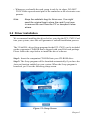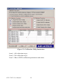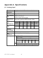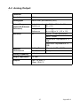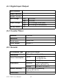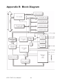
1
PCI-1742U
16-bit, 1MS/s High-Resolution
Multifunction Card
User Manual
Copyright
The documentation and the software included with this product are copyrighted 2006 by Advantech Co., Ltd. All rights are reserved. Advantech
Co., Ltd. reserves the right to make improvements in the products
described in this manual at any time without notice. No part of this manual may be reproduced, copied, translated or transmitted in any form or
by any means without the prior written permission of Advantech Co., Ltd.
Information provided in this manual is intended to be accurate and reliable. However, Advantech Co., Ltd. assumes no responsibility for its use,
nor for any infringements of the rights of third parties, which may result
from its use.
Acknowledgements
Microsoft Windows and MS-DOS are registered trademarks of
Microsoft Corp.
All other product names or trademarks are properties of their respective
owners.
Part No. 2003174200
1st Edition
Printed in Taiwan
March 2006
PCI-1742U User Manual
ii
Product Warranty (2 years)
Advantech warrants to you, the original purchaser, that each of its products will be free from defects in materials and workmanship for two years
from the date of purchase.
This warranty does not apply to any products which have been repaired or
altered by persons other than repair personnel authorized by Advantech,
or which have been subject to misuse, abuse, accident or improper installation. Advantech assumes no liability under the terms of this warranty as
a consequence of such events.
Because of Advantech’s high quality-control standards and rigorous testing, most of our customers never need to use our repair service. If an
Advantech product is defective, it will be repaired or replaced at no
charge during the warranty period. For out-of-warranty repairs, you will
be billed according to the cost of replacement materials, service time and
freight. Please consult your dealer for more details.
If you think you have a defective product, follow these steps:
1.
Collect all the information about the problem encountered. (For
example, CPU speed, Advantech products used, other hardware
and software used, etc.) Note anything abnormal and list any
onscreen messages you get when the problem occurs.
2.
Call your dealer and describe the problem. Please have your manual, product, and any helpful information readily available.
3.
If your product is diagnosed as defective, obtain an RMA (return
merchandize authorization) number from your dealer. This allows
us to process your return more quickly.
4.
Carefully pack the defective product, a fully-completed Repair and
Replacement Order Card and a photocopy proof of purchase date
(such as your sales receipt) in a shippable container. A product
returned without proof of the purchase date is not eligible for warranty service.
5.
Write the RMA number visibly on the outside of the package and
ship it prepaid to your dealer.
iii
CE
This product has passed the CE test for environmental specifications. Test conditions for passing included the equipment being operated within an industrial
enclosure. In order to protect the product from being damaged by ESD (Electrostatic Discharge) and EMI leakage, we strongly recommend the use of CE-compliant industrial enclosure products.
FCC Class A
This equipment has been tested and found to comply with the limits for a Class A
digital device, pursuant to Part 15 of the FCC Rules. These limits are designed to
provide reasonable protection against harmful interference when the equipment is
operated in a commercial environment. This equipment generates, uses and can
radiate radio frequency energy and, if not installed and used in accordance with
the instruction manual, may cause harmful interference to radio communications.
Operation of this equipment in a residential area is likely to cause harmful interference in which case the user will be required to correct the interference at own
expense.
Technical Support and Assistance
Step 1. Visit the Advantech web site at www.advantech.com/support
where you can find the latest information about the product.
Step 2. Contact your distributor, sales representative, or Advantech's customer service center for technical support if you need additional
assistance. Please have the following information ready:
- Product name and serial number
- Description of your peripheral attachments
- Description of your software (OS, version, software, etc.)
- A complete description of the problem
- The exact wording of any error messages
Packing List
Before setting up the system, check that the items listed below are
included and in good condition. If any item does not accord with the
table, please contact your dealer immediately.
• 1 x PCI-1742U card
• 1 x Companion CD-ROM (DLL driver included)
• 1 x User Manual (This manual)
PCI-1742U User Manual
iv
Contents
Chapter
Chapter
1 Introduction ..................................................... 2
1.1
1.2
Introduction ....................................................................... 2
Features ............................................................................. 2
1.3
Installation Guide .............................................................. 4
1.4
1.5
Software ............................................................................ 5
Accessories........................................................................ 6
1.2.1
1.2.2
1.2.3
1.2.4
1.2.5
Figure 1.1:Installation Flow Chart ................................. 5
1.5.1
1.5.2
1.5.3
PCL-10168 Wiring Cable .............................................. 6
ADAM-3968 Wiring Boards ......................................... 6
PCLD-8710 .................................................................... 6
2 Installation ....................................................... 8
2.1
2.2
Unpacking ......................................................................... 8
Driver Installation ............................................................. 9
2.3
Hardware Installation ...................................................... 11
2.4
Device Configuration & Testing ..................................... 13
2.5
Figure 2.1:Setup Screen ................................................. 9
Figure 2.2:Driver Setup ............................................... 10
Figure 2.3:Device Manager ......................................... 12
Figure 2.4:Device Manager Dialog Box ...................... 13
Figure 2.5:The Device Setting Dialog Box ................. 14
Device Testing................................................................. 15
2.5.1
2.5.2
2.5.3
2.5.4
2.5.5
Chapter
Auto-Calibration Function ............................................. 2
BoardID ......................................................................... 3
Plug-and-Play Function ................................................. 3
Onboard FIFO Memory ................................................. 3
Onboard Programmable Timer/Counter ........................ 3
Testing the Analog Input Function .............................. 15
Figure 2.6:Analog Input tab ......................................... 16
Testing the Analog Output Function ........................... 16
Figure 2.7:Analog Output Tab ..................................... 16
Testing Digital Input Function ..................................... 17
Figure 2.8:Digital Input Tab ........................................ 17
Testing Digital Output Function .................................. 17
Figure 2.9:Digital Output Tab ..................................... 17
Testing Counter Function ............................................ 18
Figure 2.10:Counter Tab .............................................. 18
3 Signal Connections ........................................ 20
3.1
3.2
I/O Connector.................................................................. 20
3.1.1
3.1.2
I/O Connector Signal Description ................................ 20
Pin Assignment ............................................................ 22
Figure 3.1:I/O Connector Pin Assignments ................. 22
Analog Input Connections .............................................. 23
v
Table of Contents
3.2.1
3.2.2
3.3
Analog Output Connections ........................................... 26
3.4
Trigger Source Connections ........................................... 26
3.5
3.6
Chapter
Figure 3.6:Analog Output Connections ....................... 26
3.4.1
3.4.2
Internal Pacer Trigger Connection ............................... 26
External Trigger Source Connection ........................... 27
Field Wiring Considerations .......................................... 27
BoardID Switch Settings................................................. 28
Figure 3.7:Jumpers and Switch Locations ................... 28
Table 3.2:BoardID Setting ........................................... 29
4 Software Overview ........................................ 32
4.1
4.2
4.3
Chapter
Single-ended Channel Connections ............................. 23
Figure 3.2:Single-ended Channel Connections .......... 23
Differential Channel Connections ............................... 24
Figure 3.3:Differential Connection - Ground Signal ... 24
Figure 3.4:Differential Connection - Floating Signal .. 25
Figure 3.5:Example ...................................................... 25
Software Overview.......................................................... 32
Programming Choices .................................................... 32
4.2.1
4.2.2
DLL Driver .................................................................. 32
Register-Level Programming ....................................... 32
DLL Driver Programming Roadmap ............................. 32
4.3.1
4.3.2
4.3.3
Programming Tools ..................................................... 33
Programming with DLL Driver Function Library ....... 33
Troubleshooting DLL Driver Error ............................. 34
5 Calibration ..................................................... 36
5.1
VR Assignment ............................................................... 36
5.1.1
Figure 5.1:Locations of VR1 and TP3 ......................... 36
Calibration Utility ........................................................ 37
Figure 5.2:AD and DA Auto Calibration Utility ......... 37
Figure 5.3:Calibration Utility Instruction .................... 38
Appendix A Specifications ................................................. 40
A.1
A.2
A.3
A.4
A.5
Analog Input.................................................................... 40
Analog Output:................................................................ 41
Digital Input /Output: ...................................................... 42
Counter/Timer: ................................................................ 42
General ............................................................................ 42
Appendix B Block Diagram ............................................... 44
Appendix C 82C54 Counter Chip Function..................... 46
C.1
C.2
C.3
Intel 82C54...................................................................... 46
Counter Read/Write & Control Registers ....................... 47
Counter Operating Modes ............................................... 50
PCI-1742U User Manual
vi
CHAPTER
1
2
Introduction
This chapter introduces PCI-1742U and
shows how to install the software and
information on useful accessories.
Sections include:
• Introduction
• Features
• Installation Guide
• Software
• Accessories
Chapter 1 Introduction
1.1 Introduction
Thank you for buying the Advantech PCI-1742U PCI card. PCI-1742U is
a powerful high-resolution multifunction DAS card with 1MS/s sampling
rate and 16-bit resolution, fulfills the needs of most data acquisition applications. PCI-1742U provides 16 single-ended or 8 differential analog
input channels, two 16-bit D/A output channels, 16 digital input/output
channels, and one 10 MHz 16-bit counter channel.
The following sections will provide further information about features of
the multifunction cards, a quick installation guide, and some brief information on software and accessories for the PCI-1742U card.
1.2 Features
The Advantech PCI-1742U provides users with the most requested measurement and control functions as below:
• 16 S.E.or 8 Diff. analog input channels with 1K FIFO.
• 16-bit ADC with max. 1MS/s sampling rate
• Two 16-bit analog output channels
• 16DI/16DO TTL channels
• One 16-bit/ 10MHz counter
• Auto calibration function
• Universal PCI Bus (Support 3.3/5 V PCI Bus signal)
• Board ID switch
1.2.1 Auto-Calibration Function
The PCI-1742U provides an auto-calibration function with an calibration
utility. The built-in calibration circuitry of the PCI-1742U corrects gain
and offset errors in analog input channels, thereby eliminating the need
for external equipment and user adjustments.
PCI-1742U User Manual
2
1.2.2 BoardID
The PCI-1742U has a built-in DIP switch that helps define each card’s
unique ID when multiple PCI-1742U cards have been installed on the
same PC chassis. The BoardID setting function is very useful when building a system with multiple PCI-1742U cards. With the correct BoardID
settings, you can easily identify and access each card during hardware
configuration and software programming.
1.2.3 Plug-and-Play Function
The PCI-1742U is a Plug-and-Play device, which fully complies with PCI
Specification Rev 2.2. During card installation, there is no need to set
jumpers or DIP switches. Instead, all bus-related configurations such as
base I/O address and interrupt are automatically done by the Plug & Play
function.
1.2.4 Onboard FIFO Memory
PCI-1742U provides 1K samples on-board FIFO (First In First Out)
memory buffer for AD. This is an important feature for faster data transfer and more predictable performance under the Windows system.
1.2.5 Onboard Programmable Timer/Counter
PCI-1742U provides a programmable timer counter for generating a
pacer trigger for the A/D conversion. The timer/counter chip is 82C54,
which includes three 16-bit counter 10 MHz clocks. One counter is used
as an event counter for counting events coming from the input channel.
The other two are cascaded together to make a 32-bit timer for pacer trigger time base.
3
Chapter 1
1.3 Installation Guide
Before you install your PCI-1742U card, please make sure you have the
following necessary components:
• PCI-1742U Multifunction Card
• PCI-1742U User Manual
• Driver software Advantech DLL Drivers (in the companion CD-ROM)
• Computer: PC with a PCI-bus slot running Windows 2000/XP
• Application software: ActiveDAQ, ActiveDAQ Pro, 3rd party software
After you get the necessary components and maybe some of the accessories for enhanced operation of your Multifunction card, you can then
begin the Installation procedures. Fig. 1-1 on the next page provides a
concise flow chart to give users a broad picture of the software and hardware installation procedures:
PCI-1742U User Manual
4
Figure 1.1: Installation Flow Chart
1.4 Software
Advantech offers a rich set of DLL drivers, 3rd-party driver support and
application software to help fully exploit the functions of your
PCI-1742U card:
• DLL driver (on the companion CD-ROM)
• LabVIEW driver
• Advantech ActiveDAQ
• Advantech ActiveDAQ Pro
5
Chapter 1
For more information on software, please refer to Chapter 4, Software
Overview.
Users who intend to program directly at the registers of the Multifunction
card have register-level programming as an option. Since register-level
programming is often difficult and labor-intensive, it is usually recommended only for experienced programmers. For more information, please
refer to Appendix C, Register Structure & Format.
1.5 Accessories
Advantech offers a complete set of accessory products to support the PCI1742U cards. These accessories include:
1.5.1 PCL-10168 Wiring Cable
The PCL-10168 shielded cable is specially designed for PCI-1742U cards
to provide high resistance to noise. To achieve a better signal quality, the
signal wires are twisted in such a way as to form a “twisted-pair cable”,
reducing cross-talk and noise from other signal sources. Furthermore, its
analog and digital lines are separately sheathed and shielded to neutralize
EMI/EMC problems.
1.5.2 ADAM-3968 Wiring Boards
The ADAM-3968 is a 68-pin SCSI wiring terminal module for DIN-rail
mounting. This terminal module can be readily connected to the Advantech PC-Lab cards and allow easy yet reliable access to individual pin
connections for the PCI-1742U card.
1.5.3 PCLD-8710
PCLD-8710 is a DIN-rail-mounted screw-terminal board to be used with
any PC-LabCard products with a 68-pin SCSI connector. PCLD-8710
features the following functions:
• Two additional 20-pin flat-cable connectors for digital input and output
• Reserved space on board to meet future needs for signal-conditioning
circuits (e.g. low-pass filter, voltage attenuator and current shunt)
• Industrial-grade screw-clamp terminal blocks for heavy-duty and reliable connections.
PCI-1742U User Manual
6
CHAPTER
2
2
Installation
This chapter provides a packaged item
checklist, proper instructions about
unpacking and step-by-step procedures
for both driver and card installation.
Sections include:
• Unpacking
• Driver Installation
• Hardware Installation
• Device Configuration & Testing
• Device Testing
Chapter 2 Installation
2.1 Unpacking
After receiving your PCI-1742U package, please inspect its contents first.
The package should contain the following items:
• PCI-1742U card
• Companion CD-ROM (DLL driver included)
• User Manual
The PCI-1742U card harbors certain electronic components vulnerable to
electrostatic discharge (ESD). ESD could easily damage the integrated
circuits and certain components if preventive measures are not carefully
paid attention to.
Before removing the card from the antistatic plastic bag, you should take
following precautions to ward off possible ESD damage:
• Touch the metal part of your computer chassis with your hand to discharge static electricity accumulated on your body. Or one can also use
a grounding strap.
• Touch the antistatic bag to a metal part of your computer chassis before
opening the bag.
• Take hold of the card only by the metal bracket when removing it out of
the bag.
After taking out the card, you should first:
• Inspect the card for any possible signs of external damage (loose or
damaged components, etc.). If the card is visibly damaged, please
notify our service department or the local sales representative immediately. Avoid installing a damaged card into your system.
Also pay extra caution to the following to ensure proper installation:
• Avoid physical contact with materials that could hold static electricity
such as plastic, vinyl and Styrofoam.
PCI-1742U User Manual
8
• Whenever you handle the card, grasp it only by its edges. DO NOT
TOUCH the exposed metal pins of the connector or the electronic components.
Note
Keep the antistatic bag for future use. You might
need the original bag to store the card if you have
to remove the card from the PC or transport it elsewhere.
2.2 Driver Installation
We recommend installing the driver before you plug the PCI-1742U Card
into your system, since this will guarantee a smooth installation process.
The 32-bit DLL driver Setup program for the PCI-1742U card is included
on the companion CD-ROM that is shipped with your DAS card package.
Please follow the steps below to install the driver software:
Step 1: Insert the companion CD-ROM into your CD-ROM drive.
Step 2: The Setup program will be launched automatically if you have the
Autorun function enabled on your system. When the Setup program is
launched, you’ll see the following setup screen.
Figure 2.1: Setup Screen
9
Chapter 2
Note
If the autoplay function is not enabled on your computer,
use Windows Explorer or Windows Run command to
execute Autorun.exe in the companion CD-ROM.
Step 3: Select the Installation option, then the Individual Drivers option.
Step 4: Select the specific device then just follow the installation instructions step by step to complete your device driver setup.
Figure 2.2: Driver Setup
For further information on driver-related issues, an online version of the
DLL Drivers Manual is available by accessing the following path:
Start/ Programs/ Advantech Automation/ Device Manager/ Device
Driver's Manual.
PCI-1742U User Manual
10
2.3 Hardware Installation
Note:
Make sure you install the driver before you install
the card (Refer to 2.2 Driver Installation)
After the DLL driver installation is completed, you can install the PCI1742U card in any PCI slot. It is suggested that you refer to the user manual or related documents if you have any doubts. Please follow the steps
below to install the card on your system:
Step 1: Turn off your computer and unplug the power cord and cables.
Turn off your computer before installing or removing any components.
Step 2: Remove the cover of your computer.
Step 3: Remove the slot cover on the back panel of your computer.
Step 4: Touch the metal part on the surface of your computer to neutralize
any static electricity that might be in your body.
Step 5: Insert the PCI-1742U card into a PCI slot. Hold the card only by
its edges and carefully align it with the slot. Insert the card firmly into
place. Use of excessive force must be avoided; or the card might be damaged.
Step 6: Fasten the bracket of the PCI card on the back panel rail of the
computer with screws.
Step 7: Connect appropriate accessories (68-pin cable, wiring terminals,
etc. if necessary) to the PCI card.
Step 8: Replace the cover of your computer chassis. Re-connect the
cables you removed in step 2.
Step 9: Plug in the power cord and turn on the computer.
Note
If you installed the card without installing the
DLL driver first, Windows 2000/XP will recognize
your card as an “unknown device” after rebooting, and will prompt you to provide the necessary driver. You should ignore the prompting
messages (just click the Cancel button) and set
up the driver according to the steps described in
2.2 Driver Installation.
11
Chapter 2
After the PCI-1742U card is installed, you can verify whether it is properly installed on your system in the Device Manager:
1.
Access the Device Manager through
Start/ Control Panel/ System/ Device Manager.
2.
The device name of PCI-1742U should be listed on the Device
Manager.
Figure 2.3: Device Manager
Note
If your card is properly installed, you should see
the device name of your card listed on the Device
Manager tab. If you see your device name listed,
but marked with an exclamation sign “!”, it means
your card has not been correctly installed. In this
case, remove the card device from the Device
Manager by selecting its device name and press
the Remove button. Then go through the driver
installation process again.
PCI-1742U User Manual
12
After your card is properly installed on your system, you can now configure your device using the Device Manager program that has itself already
been installed on your system during driver setup. A complete device
installation procedure should include device setup, configuration and testing. The following sections will guide you through the setup, configuration and testing of your device.
2.4 Device Configuration & Testing
The Device Manager program is a utility that allows you to configure and
test your device, and later stores your settings on the system registry.
These settings will be used when you call the APIs of Advantech Device
Drivers.
After properly installing PCI-1742U, you can now proceed to configure
and test the device by clicking the Setup/Test button on the I/O Device
Manager dialog box. (Fig. 2-4).
Figure 2.4: Device Manager Dialog Box
13
Chapter 2
Note
As we have noted, the device name "000:<PCI1742U BoardID=1 I/O=ec000H" begins with
device number "000", which is specifically
assigned to each card. The device number is
passed to the driver to specify which device you
wish to control.
Device Configuration
In the Device Setting dialog box (Figure2.5), you can configure the A/D
channel as Single-ended or Differential and choose the D/A channel reference voltage source type.
.
Figure 2.5: The Device Setting Dialog Box
PCI-1742U User Manual
14
Note
You can configure the source of D/A reference voltage either as Internal or External, and select the
output voltage range. When selecting Internal voltage source, you have four options for the output
voltage range : 0~5V, 0~10V, +/-5V & +/-10V.
When selected as External, the output voltage
range is determined by the external reference voltage in the following way:
By inputting an external reference voltage: -xV ,
where |x| <= 10, you will get two available output
voltage ranges: 0~xV and -x~xV.
2.5 Device Testing
After following the Setup and Configuration procedure to the last step
described in the previous section, you can now proceed to test the device
by clicking the Test Button on the Device Manager dialog box (Fig. 2-4).
Note:
You can access the Device Test dialog box through the
previous procedure for the Device Installation, or simply
by accessing Start/Programs/Advantech Automation/
Device Manager/Advantech Device Manager.
All functions are performed by the software polling
method. For high speed data acquirements or output,
functions have to use a corresponding VC example like
ADINT or ADBMDMA.
2.5.1 Testing the Analog Input Function
Click the Analog Input tab to bring it up to the front of the screen. Select
the input range for each channel in the Input range drop-down boxes. Configure the sampling rate on the scroll bar. Switch the channels by using the
up/down arrow.
15
Chapter 2
Figure 2.6: Analog Input tab
2.5.2 Testing the Analog Output Function
Click the Analog Output tab to bring it up to the foreground. The Analog
Output tab allows you to output quasi-sine, triangle, or square waveforms
automatically, or output single values manually. You can also configure
the waveform frequency and output voltage range.
Figure 2.7: Analog Output Tab
PCI-1742U User Manual
16
2.5.3 Testing Digital Input Function
Click the Digital Input tab to show forth the Digital Input test panel as
seen below. Through the color of the lamps, you can easily discern
whether the status of each digital input channel is high or low.
Figure 2.8: Digital Input Tab
2.5.4 Testing Digital Output Function
Click the Digital Output tab to bring up the Digital Output test panel such
as the one seen on the next page. By pressing the buttons on each tab, you
can easily set each digital output channel as high or low for the corresponding port.
Figure 2.9: Digital Output Tab
17
Chapter 2
2.5.5 Testing Counter Function
Click the Counter Tab to bring its test panel forth. The counter channel
(Channel 0) offers two options: Event counting and Pulse out. If you
select Event counting, you need to connect your clock source to pin
CNT0_CLK. If you select Pulse Out, the clock source will be output to
pin CNT0_OUT. You can configure the Pulse Frequency with the scroll
bar right below it.
Figure 2.10: Counter Tab
Only after your card device is properly set up, configured and tested, can
the device installation procedure be counted as complete. After the device
installation procedure is completed, you can safely proceed to the next
chapter, Signal Connections.
PCI-1742U User Manual
18
CHAPTER
2
3
Signal Connections
This chapter provides useful information about how to connect input and
output signals to PCI-1742U via the I/O
connector.
Sections include:
• I/O Connector
• Analog Input Connections
• Analog Output Connections
• Trigger Source Connections
• Field Wiring Considerations
Chapter 3 Signal Connections
3.1 I/O Connector
The I/O connector on the PCI-1742U is a 68-pin connector that enables
you to connect to accessories with the PCL-10168 shielded cable.
Fig. 3-1 shows the pin assignments for the 68-pin I/O connector on the
PCI-1742U, and table 3-1 shows the I/O connector signal description.
3.1.1 I/O Connector Signal Description
Table 3.1: I/O Connector Signal Description
AI<0…15>
AIGND
Input
Analog Input Channels 0 through 15.
Each channel pair, AI<i, i+1> (i = 0, 2,
4...14), can be configured as either two
single-ended inputs or one differential
input.
AIGND
-
-
Analog Input Ground. The three ground
references (AIGND, AOGND, and
DGND) are connected together.
AO0_REF
AO1_REF
AOGND
Input
Analog Output Channel 0/1 External Reference.
AO0_OUT
AO1_OUT
AOGND
Output Analog Output Channels 0/1
AOGND
-
-
Analog Output Ground. The analog output voltages are referenced to these
nodes. The three ground references
(AIGND, AOGND, and DGND) are connected together.
DI<0..15>
DGND
Input
Digital Input channels.
DO<0..15>
DGND
Output Digital Output channels.
DGND
-
-
PCI-1742U User Manual
Digital Ground. This pin supplies the reference for the digital channels at the I/O
connector as well as the +5VDC supply.
The three ground references (AIGND,
AOGND, and DGND) are connected
together.
20
Table 3.1: I/O Connector Signal Description
CNT0_CLK
DGND
Input
Counter 0 Clock Input. The clock input of
counter 0 can be either external or internal , as set by software.
CNT0_OUT
DGND
Output Counter 0 Output.
CNT0_GATE
DGND
Input
PACER_OUT
DGND
Output Pacer Clock Output. This pin pulses
once for each pacer clock when turned
on. If A/D conversion is in the pacer trigger mode, users can use this signal as a
synchronous signal for other applications.
TRG_GATE
DGND
Input
A/D External Trigger Gate. When TRG
_GATE is connected to DGND, it will disable the external trigger signal to input.
EXT_TRG
DGND
Input
A/D External Trigger. This pin is external
trigger signal input for the A/D conversion. A low-to-high edge triggers A/D
conversion to start.
+12V
DGND
Output +12 VDC Source.
+5V
DGND
Output +5 VDC Source.
Counter 0 Gate Control.
21
Chapter 3
3.1.2 Pin Assignment
Figure 3.1: I/O Connector Pin Assignments
PCI-1742U User Manual
22
3.2 Analog Input Connections
3.2.1 Single-ended Channel Connections
The single-ended input configuration has only one signal wire for each
channel, and the measured voltage (Vm) is the voltage of the wire as referenced against the common ground.
A signal source without a local ground is also called a “floating source”.
It is fairly simple to connect a single-ended channel to a floating signal
source. In this mode, the PCI-1742U provides a reference ground for
external floating signal sources. Fig. 3-2 shows a single-ended channel
connection between a floating signal source and an input channel on PCI1742U.
Figure 3.2: Single-ended Channel Connections
23
Chapter 3
3.2.2 Differential Channel Connections
The differential input channels operate with two signal wires for each
channel, and the voltage difference between both signal wires is measured. On PCI-1742U, when all channels are configured to differential
input, up to 8 analog channels are available.
If one side of the signal source is connected to a local ground, the signal
source is ground-referenced. Therefore, the ground of the signal source
and the ground of the card will not be exactly of the same voltage. The
difference between the ground voltages forms a common-mode voltage
(V cm ).
To avoid the ground loop noise effect caused by common-mode voltages,
you can connect the signal ground to the Low input. Figure 3-3 shows a
differential channel connection between a ground-reference signal source
and an input channel on the PCI-1742U. With this connection, the PGIA
rejects a common-mode voltage Vcm between the signal source and the
PCI-1742U ground, shown as Vcm in Figure 3-3.
Figure 3.3: Differential Connection - Ground Signal
PCI-1742U User Manual
24
If a floating signal source is connected to the differential input channel,
the signal source might exceed the common-mode signal range of the
PGIA, and the PGIA will be saturated with erroneous voltage-readings.
You must therefore reference the signal source against the AIGND.
Figure 3.4 shows a differential channel connection between a floating
signal source and an input channel on PCI-1742U. In this figure, each
side of the floating signal source is connected through a resistor to the
AIGND. This connection can reject the common-mode voltage between
the signal source and the PCI-1742U ground.
Figure 3.4: Differential Connection - Floating Signal
This connection has the disadvantage of loading the source down with the
series combination (sum) of the two resistors. For ra and rb, for example,
if the input impedance rs is 1 kW, and each of the two resistors are 100
kW, then the resistors load down the signal source with 200 kW (100 kW
+ 100 kW), resulting in a –0.5% gain error. The following gives a simplified representation of the circuit and calculating process.
25
Chapter 3
Figure 3.5: Example
3.3 Analog Output Connections
The PCI-1742U provides two D/A output channels, AO0 and AO1. You
may use the PCI-1742U internally-provided precision -5V (-10V) reference to generate 0 to +5 V (+10 V) D/A output range. You may also create a D/A output range through the external reference, AO0_REF. The
external reference input range is +/-10 V. For example, connecting with
an external reference of -7 V will generate 0 ~ +7 V D/A output.
Fig. 3-5 shows how to make analog output and external reference input
connections on the PCI-1742U.
Figure 3.6: Analog Output Connections
PCI-1742U User Manual
26
3.4 Trigger Source Connections
3.4.1 Internal Pacer Trigger Connection
PCI-1742U includes one 82C54 compatible programmable Timer/
Counter chip which provides three 16-bit counters connected to a 10
MHz clock, each designated specifically as Counter 0, Counter 1 and
Counter 2. Counter 0 is a counter which counts events from an input
channel or outputting pulse. Counter 1 and Counter 2 are cascaded to create a 32-bit timer for pacer triggering. A low-to-high edge from the
Counter 2 output (PACER_OUT) will trigger an A/D conversion on the
PCI-1742U. At the same time, you can also use this signal as a synchronous signal for other applications.
3.4.2 External Trigger Source Connection
In addition to pacer triggering, the PCI-1742U also allows external triggering for A/D conversions. A low-to-high edge coming from
EXT_TRG will trigger an A/D conversion on the PCI-1742U. When
DGND is connected to TRG_GATE, the external trigger function is
thereby disabled.
3.5 Field Wiring Considerations
When you use the PCI-1742U to acquire data from outside, noises in the
environment might significantly affect the accuracy of your measurements if due cautions are not taken. The following measures will be helpful to reduce possible interference running signal wires between signal
sources and the PCI-1742U.
• The signal cables must be kept away from strong electromagnetic
sources such as power lines, large electric motors, circuit breakers or
welding machines, since they may cause strong electromagnetic interference. Keep the analog signal cables away from any video monitor,
since it can significantly affect a data acquisition system.
• If the cable travels through an area with significant electromagnetic
interference, you should adopt individually shielded, twisted-pair wires
as the analog input cable. This type of cable has its signal wires twisted
together and shielded with a metal mesh. The metal mesh should only
be connected to one point at the signal source ground.
• Avoid running the signal cables through any conduit that might have
power lines in it.
27
Chapter 3
• If you have to place your signal cable parallel to a power line that has a
high voltage or high current running through it, try to keep a safe distance between them. Or, you should place the signal cable at a right
angle to the power line to minimize the undesirable effect.
The signals transmitted on the cable will be directly affected by the quality of the cable. In order to ensure better signal quality, we recommend
that you use the PCL-10168 shielded cable.
3.6 BoardID Switch Settings
The PCI-1742U card has one Board ID switch setting. The following
image shows the layout of PCI-1742U
:
Figure 3.7: Jumpers and Switch Locations
The PCI-1742U has a built-in DIP-switch (SW1), which is used to define
each the BoardID. You can determine the BoardID switch on the register.
When there are multiple cards on the same chassis, this BoardID switch
setting function is useful for identifying each card device number through
BoardID switch. The factory setting for the PCI-1742U BoardID switch
is 0. If you need to adjust it to other BoardID switchs, set SW1 while
referring to Table 3.2.
PCI-1742U User Manual
28
Table 3.2: BoardID Setting
ID3*
ID2
ID1
ID0
Board ID
1
1
1
1
0
1
1
1
0
1
1
1
0
1
2
1
1
0
0
3
1
0
1
1
4
1
0
1
0
5
1
0
0
1
6
1
0
0
0
7
0
1
1
1
8
0
1
1
0
9
0
1
0
1
10
0
1
0
0
11
0
0
1
1
12
0
0
1
0
13
0
0
0
1
14
0
0
0
0
15
Note: On: 1, Off: 0
*ID3: the most significant bit (MSB) of BoardID
29
Chapter 3
PCI-1742U User Manual
30
CHAPTER
4
2
Software Overview
This chapter gives you an overview of
the software programming choices
available and a quick reference of
source codes.
Sections include:
• Software Overview
• Programming Choices
• DLL Driver Programming
Chapter 4 Software Overview
4.1 Software Overview
Programming choices for DAS cards: You may use Advantech application software such as Advantech DLL driver. On the other hand,
advanced users are allowed another option for register-level programming, although not recommended due to its laborious and time-consuming nature.
4.2 Programming Choices
4.2.1 DLL Driver
The Advantech DLL Drivers software is included on the companion CDROM at no extra charge. It also comes with all the Advantech DAS cards.
Advantech’s DLL driver features a complete I/O function library to help
boost your application performance. The Advantech DLL driver for Windows 2000/XP works seamlessly with development tools such as Visual
C++, Visual Basic, Borland C++ Builder and Borland Delphi.
4.2.2 Register-Level Programming
Register-level programming is reserved for experienced programmers
who find it necessary to write code directly at the level of device registers. Since register-level programming requires much effort and time, we
recommend that you use the Advantech DLL drivers instead. However, if
register-level programming is indispensable, you should refer to the relevant information in Appendix C, Register Structure and Format, or to the
example codes included on the companion CD-ROM.
4.3 DLL Driver Programming Roadmap
This section will provide you a roadmap to demonstrate how to build an
application from scratch using Advantech DLL driver with your favorite
development tools such as Visual C++, Visual Basic, Delphi and C++
Builder. The step-by-step instructions on how to build your own applications using each development tool will be given in the DLL Drivers Manual. Moreover, a rich set of example source codes are also given for your
reference.
PCI-1742U User Manual
32
4.3.1 Programming Tools
Programmers can develop application programs with their favorite development tools:
• Visual C++
• Visual Basic
• Delphi
• C++ Builder
For instructions on how to begin programming in each development tool,
Advantech offers a Tutorial Chapter in the DLL Drivers Manual for your
reference. Please refer to the corresponding sections in this chapter on the
DLL Drivers Manual to begin your programming efforts. You can also
take a look at the example source codes provided for each programming
tool, since they can be very helpful.
The DLL Drivers Manual can be found on the companion CD-ROM. Or
if you have already installed the DLL Drivers on your system, The DLL
Drivers Manual can be readily accessed through the Start button:
Start/Programs/Advantech Automation/Device Manager/Device
Driver's Manual
The example source codes can be found under the corresponding installation folder such as the default installation path:
\Program Files\ADVANTECH\ADSAPI\Examples
For information about using other function groups or development tools,
please refer to the Creating Windows 2000/XP Application with DLL
Driver and the Function Overview chapters in the DLL Drivers Manual.
4.3.2 Programming with DLL Driver Function Library
Advantech DLL driver offers a rich function library to be utilized in various application programs. This function library consists of numerous
APIs that support many development tools, such as Visual C++, Visual
Basic, Delphi and C++ Builder.
33
Chapter 4
According to their specific functions or services, these APIs can be categorized into several function groups:
• Analog Input Function Group
• Analog Output Function Group
• Digital Input/Output Function Group
• Counter Function Group
• Port Function Group
For the usage and parameters of each function, please refer to the Function Overview chapter in the DLL Drivers Manual.
4.3.3 Troubleshooting DLL Driver Error
Driver functions will return a status code when they are called to perform
a certain task for the application. When a function returns a code that is
not zero, it means the function has failed to perform its designated function. To troubleshoot the DLL driver error, you can pass the error code to
DRV_GetErrorMessage function to return the error message. Or you
can refer to the DLL Driver Error Codes Appendix in the DLL Drivers
Manual for a detailed listing of the Error Code, Error ID and the Error
Message.
PCI-1742U User Manual
34
CHAPTER
5
2
Calibration
This chapter provides brief information
on PCI-1742U calibration.
Sections include:
• VR Assignment
Chapter 5 Calibration
PCI-1742U has been calibrated at the factory for initial use. However, a
calibration of the analog input and the analog output function every six
months is recommended.
These calibration programs make calibration an easy job. With a variety
of prompts and graphic displays, these programs will lead you through
the calibration and setup procedures, showing you all the correct settings
and adjustments.
To perform a satisfactory calibration, you will need a 7½-digit digital
multi-meter and a voltage calibrator or a stable, noise-free D.C. voltage
source.
Note
Before you calibrate the PCI-1742U, you must
turn on the power at least 15 minutes to make
sure the DAS card is stable.
5.1 VR Assignment
There is one variable resistor (VR1) on the PCI-1742U to adjust the accurate reference voltage on the PCI-1742U. We provide a test point (See
TP3 in Figure 5.1) for you to check the reference voltage on board.
Before you start to calibrate A/D and D/A channels, please adjust VR1
until the reference voltage on TP3 has reached +5.0000 V. Figure 5.1
shows the locations of VR1 and TP3.
Figure 5.1: Locations of VR1 and TP3
PCI-1742U User Manual
36
5.1.1 Calibration Utility
Users can access the "AD and DA Auto Calibration" utility through the
Advantech Device Manger
Figure 5.2: AD and DA Auto Calibration Utility
Please follow the utility instructions to complete AD/DA calibration.
37
Chapter 5
Figure 5.3: Calibration Utility Instruction
Item 1: AD calibration steps;
Item 2: DA calibration steps;
Item 3: Show AD/DA calibration parameters and status.
PCI-1742U User Manual
38
APPENDIX
A
2
Specifications
Appendix A Specifications
A.1 Analog Input
Channels
16 single-ended or 8 differential or combination
Resolution
16-bit
FIFO Size
1K samples
Max. Sampling 1 MS/s single-channel
800kS/s multi-channel
Rate
250kS/s unipolar bipolar mixed
A/D converter Normal mode: maximum 800kS/s minimum: no
Warp mode: maximum 1MS/s minimum: 1kS/s
mode
Input range
and
PGA Gain List
Bandwidth of
PGA
Common
Mode Voltage
PGA Gain 0.5
1
Unipolar
N/A
0~10
Bipolar
±10
±5
PGA Gain 0.5
1
Band2MHz 2MHz
width
±7 V max. (operational)
2
0~5
±2.5
2
1MHz
4
0~2.5
±1.25
4
1MHz
8
0~1.25
±0.625
8
800kHz
Protection
±20 V
Input
Impedance
100 M/10pF(Off); 100 M/100pF(On)
Accuracy
DC DNLE: ±1LSB
INLE: ±3LSB
Offset error: Adjustable to ±2 LSB
Gain
0.5
1
2
4
8
Gain error 0.02 0.02 0.02 0.03 0.04
(% FSR)
AC THD: -90 dB
ENOB: 13.5 bits @ 1MS/s 14.5 bits @ < 250KS/s
PCI-1742U User Manual
40
A.2 Analog Output:
Channels
2
Resolution
16-bit
Throughput
2MS/s max. per channel (FSR)
Output Range
(Internal & External
Reference)
Using Internal
Reference
0~+5V, 0~+10 V, -5~+5V,10~+10V
Using External
Reference
0~+x V@ +x V (-10 x 10)
-x~+x V@ +x V (-10 x 10)
Accuracy
DC
DNLE: ±1LSB (monotonic)
INLE: ±2LSB
Offset error: Adjustable to ±2
LSB
Gain error: Adjustable to ±2
LSB
Dynamic
Performance
Settling Time
0.5µs (to 4 LSB of FSR)
Slew Rate
40 V/µs
Driving Capability
±20mA
Output Impedance
2.5 ohm
Tempco
Gain: 30 ppm/°C
Offset: 15µV/°C
41
Appendix A
A.3 Digital Input /Output:
Input channels
16
Output channels
16
Number of ports
2
Input Voltage
Low
Output Voltage
Pull up resistor
0.8 V max.
High
2.0 V min.
Low
0.5 V max.@+24 mA (sink)
High
2.4 V min.@-15 mA (source)
10k
A.4 Counter/Timer:
Channels
1 (82C54)
Resolution
16-bit
Clock source
10MHz max.
Clock Tempco
50 ppm/°C
A.5 General
I/O Connector Type
68-pin SCSI-II female
Dimensions
175 × 100 mm (6.9" × 3.9")
Power Consumption
Typical
+5 V @ 850 mA
+12 V @ 600 mA
Max.
+5 V @ 1 A
Operation
0~+60°C (32~158°F)
(refer to IEC 68-2-1,2)
Storage
-20~+85°C (-4~185°F)
Temperature
Relative Humidity
5 ~ 95% RH non-condensing
(refer to IEC 68-2-3)
Certification
CE certified
PCI-1742U User Manual
42
APPENDIX
B
2
Block Diagram
Appendix B Block Diagram
PCI-1742U User Manual
44
APPENDIX
2
C
82C54 Counter Chip
Function
Appendix C 82C54 Counter Chip
Function
C.1 Intel 82C54
The PCI-1742U uses one Intel 82C54-compatible programmable interval
timer/counter chip. The popular 82C54 chip offers three independent 16bit counters, counter 0, counters 1 and 2. You can program each counter
for maximum count values from 2 to 65535.
The 82C54 has a maximum input clock frequency of 10 MHz. The PCI1742U provides 10 MHz input frequencies to the counter chip from an
onboard crystal oscillator.
Counter 0
On the PCI-1742U, counter 0 can be a 16-bit timer or an event counter as
chosen by the user. When the clock source is set as an internal source,
counter 0 is a 16-bit timer.
Counter 1 & 2
Counters 1 and 2 of the counter chip are cascaded to create a 32-bit timer
for the pacer trigger. A low-to-high edge of counter 2’s output will trigger
an A/D conversion.
PCI-1742U User Manual
46
C.2 Counter Read/Write & Control Registers
The 82C54 programmable interval timer uses four registers at addresses
BASE + 24 (Dec), BASE + 26 (Dec), BASE + 28 (Dec) and BASE + 30
(Dec) for read, write and control of counter functions. Register functions
appear below:
Table C.1: Counter Registers
Register
Function
BASE + 24 (Dec)
Counter 0 read/write
BASE + 26 (Dec
Counter 1 read/write
BASE + 28 (Dec)
Counter 2 read/write
BASE + 30 (Dec)
Counter control word
Since the 82C54 counter uses a 16-bit structure, each section of read/
write data is split into a least significant byte (LSB) and most significant
byte (MSB). To avoid errors, it is important that you make read/write
operations in pairs and keep track of the byte order.
The data format for the control register is as below:
BASE + 30 (Dec) 82C54 control
Bit
D7
D6
D5
D4
D3
D2
D1
D0
Value
SC1
SC0
RW1
RW0
M2
M1
M0
BCD
Description
SC1 & SC0 Select counter
Counter
SC1
SC0
0
0
0
1
0
1
2
1
0
Read-back command
1
1
47
Appendix C
RW1 & RW0 Select read / write operation
Operation
RW1
RW0
counter Latch
0
0
Read/write LSB
0
1
Read/write MSB
1
0
Read/write LSB first, then MSB
1
1
M2, M1 & M0 Select operating mode
M2
M1
M0
Mode
Description
0
0
0
0
Stop on terminal count
0
0
1
1
Programmable one shot
X
1
0
2
Rate generator
X
1
1
3
Square wave rate generator
1
0
0
4
Software triggered strobe
1
0
1
5
Hardware triggered strobe
BCD Select binary or BCD counting
BCD
Type
0
Binary counting 16-bits
1
Binary coded decimal (BCD) counting
If you set the module for binary counting, the count can be any number
from 0 up to 65535. If you set it for BCD (Binary Coded Decimal) counting, the count can be any number from 0 to 9999.
PCI-1742U User Manual
48
If you set both SC1 and SC0 bits to 1, the counter control register is in
read-back command mode. The control register data format then
becomes:
BASE + 30(Dec) 82C54 control, read-back mode
Bit
D7
D6
D5
D4
D3
D2
D1
D0
Value
1
1
CNT
STA
C2
C1
C0
X
CNT = 0
Latch count of selected counter(s)
STA = 0
Latch status of selected counter(s)
C2, C1 & C0
Select counter for a read-back operation
C2 = 1 select Counter 2
C1 = 1 select Counter 1
C0 = 1 select Counter 0
If you set both SC1 and SC0 to 1 and STA to 0, the register selected by
C2 to C0 contains a byte which shows the status of the counter. The data
format of the counter read/write register then becomes:
BASE +24/26/28(Dec) Status read-back mode
Bit
D7
D6
D5
D4
D3
D2
D1
D0
Value
OUT
NC
RW1
RW2
M2
M1
M0
BCD
OUT Current state of counter output
NC
Null count is 1 when the last count written to the counter register
has been loaded into the counting element
49
Appendix C
C.3 Counter Operating Modes
The 82C54 programmable interval timer uses four registers at addresses
BASE + 24 (Dec), BASE + 26 (Dec), BASE + 28 (Dec) and BASE + 30
(Dec) for read, write and control of counter functions.
Register functions appear below:
MODE 0 - Stop on Terminal Count
The output will initially below after you set operation to this mode. After
you load the count into the selected count register, the output will remain
low and the counter will count. When the counter reaches the terminal
count, its output will go high and remain high until you reload it with the
mode or a new count value. The counter continues to decrement after it
reaches the terminal count. Rewriting a counter register during counting
has the following results:
1.
Writing to the first byte stops the current counting.
2.
Writing to the second byte starts the new count.
MODE 1 - Programmable One-shot Pulse
The output is initially high. The output will go low on the count following
the rising edge of the gate input. It will then go high on the terminal
count. If you load a new count value while the output is low, the new
value will not affect the duration of the one-shot pulse until the succeeding trigger. You can read the current count at any time without affecting
the one-shot pulse. The one-shot is re-triggerable, thus the output will
remain low for the full count after any rising edge at the gate input.
MODE 2 - Rate Generator
The output will be low for one period of the input clock. The period from
one output pulse to the next equals the number of input counts in the
counter register. If you reload the counter register between output pulses,
the present period will not be affected, but the subsequent period will
reflect the value.
The gate input, when low, will force the output high. When the gate input
goes high, the counter will start from the initial count. You can thus use
the gate input to synchronize the counter.
PCI-1742U User Manual
50
With this mode the output will remain high until you load the count register. You can also synchronize the output by software.
MODE 3 - Square Wave Generator
This mode is similar to Mode 2, except that the output will remain high
until one half of the count has been completed (for even numbers), and
will go low for the other half of the count. This is accomplished by
decreasing the counter by two on the falling edge of each clock pulse.
When the counter reaches the terminal count, the state of the output is
changed, the counter is reloaded with the full count and the whole process
is repeated.
If the count is odd and the output is high, the first clock pulse (after the
count is loaded ) decrements the count by 1. Subsequent clock pulses decrement the count by 2. After time-out, the output goes low and the full
count is reloaded. The first clock pulse (following the reload) decrements
the counter by 3. Subsequent clock pulses decrement the count by two
until time-out, then the whole process is repeated. In this way, if the count
is odd, the output will be high for (N+1)/2 counts and low for (N-1)/2
counts.
MODE 4 - Software-Triggered Strobe
After the mode is set, the output will be high. When the count is loaded,
the counter will begin counting. On terminal count, the output will go low
for one input clock period then go high again. If you reload the count register during counting, the new count will be loaded on the next CLK
pulse. The count will be inhibited while the GATE input is low.
MODE 5 - Hardware-Triggered Strobe
The counter will start counting after the rising edge of the trigger input
and will go low for one clock period when the terminal count is reached.
The counter is re-triggerable.
51
Appendix C
PCI-1742U User Manual
52