1
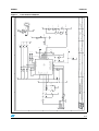
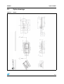
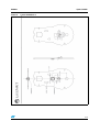
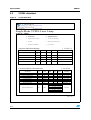
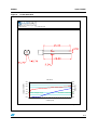
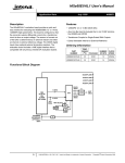
UM0441
User manual
VT5363 laser reference design mouse
Introduction
This user manual, along with the VT5363 datasheet will enable you to evaluate the VT5363
laser reference design mouse and assist you in the design of your own VT5363 laser wired
mouse. If you have any questions, support can be obtained through the normal regional
sales/support groups.
Kit contents
■
Mini reference design mouse
■
5 x VT5363V032 optical mouse sensor
■
3 x Optics - see Chapter 2
■
5 x VCSEL
Table 1.
Device summary
Order code
STV-363-R03
July 2007
Description
VT5363 laser wired mini reference design mouse
Rev 1
1/12
www.st.com
Hardware
UM0441
1
Hardware
1.1
Bill of materials
Table 2.
Laser mouse BOM
Ref.
Description
Manufacturer
Part Number
U1
Optical mouse sensor
STMicroelectronics
VT5363V032
Optics
LML 853 slim type
Luxnet
LML 853
D1
VCSEL LD851
Luxnet
LD 851
SW1,SW2,SW3
2 pin switch (DIP type)
Standard component - many suppliers
SWM
Mechanical encoder (ZWheel)
Standard component - many suppliers
C1,C4,C5,C6
4.7uF tantalum capacitor
Standard component - many suppliers
C2,C7
104pF ceramic capacitor
Standard component - many suppliers
C8,C9
15pF ceramic capacitor
Standard component - many suppliers
Q1,Q2
PNP Transistor - MMBT3906
Standard component - many suppliers
Q4
NPN Transistor - MMBT3904
Standard component - many suppliers
R2,R2A
100R resistor
Standard component - many suppliers
R6
220R resistor
Standard component - many suppliers
R1,R5,R7
4K7 resistor
Standard component - many suppliers
R14
1K5 resistor
Standard component - many suppliers
R3,R4,R8,R9,
R10,R11,R12
100K resistor
Standard component - many suppliers
R15,R16
15R resistor
Standard component - many suppliers
Y1
6MHz resonator
Standard component - many suppliers
D2
Diode 1N4148
Standard component - many suppliers
R7, R17, C3,
Q3, D3
Not fitted
1.2
Schematic
See Figure 1: Laser mouse schematic.
2/12
R
A
STMicroelectronics
R16
15R
VDD3 14
15
NC4 12
9
B
DP/CLK 13
4U7
C4
-
+
17
18
19
20
4U7
C5
1V8
3V3
3V3
C
363
VT5363 laser wired mini reference design mouse
AVRE18 16
Sheet Name:
Design Name:
-
+
LNK_LED
TRK_LED
DVDD2
DGND2
21
22
23
24
N/F
This drawing is the property of STMicroelectronics and must not be copied or
reproduced in any way without the written permission of STMicroelectronics
R15
15R
4U7
C6
U?
32OTQFP
VT5363
SDA
SCL
ZA
ZB
R17
1K
5
USB
DATA/D-
CLOCK/D+
5
-
+
DGND1
100N
C7
PULLUP 10
VDD
15PF
15PF
DVDD1
XI
NC3
32 AGND
C9
8
7
6
31 AVDD
C8
6.0MHZ
Y1
DN/DAT 11
4
100N
C2
30 TEST
3
4U7
C1
XO
DVRE18
2
1
-
+
NC2
VDD5
29 SWRIGHT
5
4
3
NC1
VREG33
R12
100K
R11
100K
N/F
Dwg. No:
Drawn By:
1V8
100N
C3
ZA
ZB
SW3
SW2
SW1
D
363-R03
MID
LHS
RHS
D
R7
4K7
N/F
3V3
Rev:
Date:
Q3
N/F
N/F
D3
A
MMBT3906
MMBT3904
ZB
ZA
R4
100K
4
J1
1
2
1
28 SWLEFT
1N4148
D2
2
1V8
R10
100K
R9
100K
R8
100K
27 SWMID
3
2
3V3
C
R6
220R
1
B
25 SWFOR
R14
1K5
Ver:
000
06-06-07
R1
4K7
Q1
Q2
Z-WHEEL
C
B
A
E
Sheet Size:
A3
SHEET 1
MMBT3904
MMBT3906
SOT
Q4
E
ENCODER
SOT
3V3
D1
3V3
R3
100K
R5
4K7
26 SWBACK
R2A
100R
OF
1
5
4
3
2
1
Figure 1.
R2
100R
A
UM0441
Hardware
Laser mouse schematic
3/12
Optics/VCSEL
UM0441
2
Optics/VCSEL
2.1
Manufacturer
STMicroelectronics has worked with an optical component / VCSEL supplier to produce a
single piece light guide and laser bundle, for more information please contact.
Luxnet Corporation
No. 50, Lung-Yuan 7th Road,
Lung-Tan Tao-Yuan Hsien,
Taiwan
Tel: 886-3-409-1335
Fax: 886-3-409-1339
http://www.luxnetcorp.com
The Luxnet optics and VCSEL order codes are detailed in Table 3 below.
Table 3.
Luxnet order codes
Part number
4/12
Description
LML 853
Laser optics
LD 851
SIngle-mode VCSEL laser lamp
UM0441
Optics/VCSEL
2.2
Optics drawings
Figure 2.
Optics
5/12
Optics/VCSEL
Figure 3.
6/12
Layout guidelines 1
UM0441
UM0441
Figure 4.
Optics/VCSEL
Layout guidelines 2
7/12
Optics/VCSEL
UM0441
2.3
VCSEL datasheet
Figure 5.
LD 851 datasheet
www.luxnetcorp.com
No. 50, Lung-Yuan 7th Road, Lung-Tan Tao-Yuan Hsien, TAIWAN
Tel: +886-3-409-1335
Fax: +886-3-409-1339
Single-Mode VCSEL Laser Lamp
Model No : LD851
• Features
• Applications
•
High resistance to ESD
•
10º~12º Far field angle
•
Superior
•
Weather-resistance Epoxy
•
Suitable for Solid State
•
Laser Mouse
( Ta=25 ºC)
Absolute Maximum Ratings
Parameter
Symbol
Unit
Min.
Max.
Forward Current
Imax
mA
Reverse Voltage
Vr
V
5
Operating Temperature
Top
°C
0
45
Storage Temperature
Tstg
°C
- 40
85
Maximum Die Exposure
Tmax
°C
Note
12
Ir =
260
for 10 sec.
( Ta=25 ºC)
Electrical/Optical Characteristics
Unit
Min.
Typ.
Max.
Threshold Current
Operating Voltage
Differential Resistance
Reverse Voltage
Slope Efficiency
Side Mode Suppression Ration
Peak Wavelength
Beam Divergence
Symb
ol
Ith
Vop
Rs
Vr
η
SMSR
λ
θ
mA
V
Ω
V
mW/mA
dB
nm
deg
1
2
2.0
60
3
2.5
130
Optical Output Power
Po
mW
Parameter
−10uA
5
0.1
20
830
0.2
0.35
30
845
860
12
Bin 1: 0.40mW~0.45mW
Bin 2: 0.45mW~0.50mW
Bin 3: 0.50mW~0.55mW
Bin 4: 0.55mW~0.60mW
Bin 5: 0.60mW~0.65mW
Bin 6: 0.65mW~0.70mW
Test
Condition
@0.5 mW
If = 5 mA
Ir= −10 μA
If = 5 mA
@0.5 mW
@ 0.5 mW
full width, 1/e2
@3.5mA
Page 1 of 3
8/12
UM0441
Optics/VCSEL
Figure 6.
LD 851 datasheet
www.luxnetcorp.com
No. 50, Lung-Yuan 7th Road, Lung-Tan Tao-Yuan Hsien, TAIWAN
Tel: +886-3-409-1335
Fax: +886-3-409-1339
3.0
2.5
2.5
2.0
2.0
1.5
1.5
1.0
1.0
Forward Voltage VF(V)
voltage (V)
output power (mW)
LIV curve
3.0
Forward Current IF(mA)
0.5
0.5
0.0
0.0
0
1
2
3
4
5
6
7
8
9
10
current (mA)
Page 2 of 3
9/12
Optics/VCSEL
Figure 7.
UM0441
LD 851 datasheet
www.luxnetcorp.com
No. 50, Lung-Yuan 7th Road, Lung-Tan Tao-Yuan Hsien, TAIWAN
Tel: +886-3-409-1335
Fax: +886-3-409-1339
Far Field Angle
ISSUE
VERSION:
DATE:
1
DRAWING NO:
ENGINEER:
2007/1/1
CHECKER:
APPROVER:
LD851
Page 3 of 3
10/12
UM0441
2.4
Revision history
VCSEL binning details
There are 5 separate grades for the VCSEL laser. As part of the manufacturing process the
VCSELs are manually sorted into the 5 grades which means for the mouse manufacturers it
is a simple process of choosing the right resistor combination for the grade of laser received.
Table 4.
VCSEL binning
Bin grade
R2 + R2A value
1
80R
2
120R
3
150R
4
200R
5
230R
The value required for R2+R2A (see Figure 1) will be clearly indicated on the label (e.g. Bin
match: 150 ohm).
3
Revision history
Table 5.
Document revision history
Date
Revision
12-Jul-2007
1
Changes
Initial release.
11/12
UM0441
Please Read Carefully:
Information in this document is provided solely in connection with ST products. STMicroelectronics NV and its subsidiaries (“ST”) reserve the
right to make changes, corrections, modifications or improvements, to this document, and the products and services described herein at any
time, without notice.
All ST products are sold pursuant to ST’s terms and conditions of sale.
Purchasers are solely responsible for the choice, selection and use of the ST products and services described herein, and ST assumes no
liability whatsoever relating to the choice, selection or use of the ST products and services described herein.
No license, express or implied, by estoppel or otherwise, to any intellectual property rights is granted under this document. If any part of this
document refers to any third party products or services it shall not be deemed a license grant by ST for the use of such third party products
or services, or any intellectual property contained therein or considered as a warranty covering the use in any manner whatsoever of such
third party products or services or any intellectual property contained therein.
UNLESS OTHERWISE SET FORTH IN ST’S TERMS AND CONDITIONS OF SALE ST DISCLAIMS ANY EXPRESS OR IMPLIED
WARRANTY WITH RESPECT TO THE USE AND/OR SALE OF ST PRODUCTS INCLUDING WITHOUT LIMITATION IMPLIED
WARRANTIES OF MERCHANTABILITY, FITNESS FOR A PARTICULAR PURPOSE (AND THEIR EQUIVALENTS UNDER THE LAWS
OF ANY JURISDICTION), OR INFRINGEMENT OF ANY PATENT, COPYRIGHT OR OTHER INTELLECTUAL PROPERTY RIGHT.
UNLESS EXPRESSLY APPROVED IN WRITING BY AN AUTHORIZED ST REPRESENTATIVE, ST PRODUCTS ARE NOT
RECOMMENDED, AUTHORIZED OR WARRANTED FOR USE IN MILITARY, AIR CRAFT, SPACE, LIFE SAVING, OR LIFE SUSTAINING
APPLICATIONS, NOR IN PRODUCTS OR SYSTEMS WHERE FAILURE OR MALFUNCTION MAY RESULT IN PERSONAL INJURY,
DEATH, OR SEVERE PROPERTY OR ENVIRONMENTAL DAMAGE. ST PRODUCTS WHICH ARE NOT SPECIFIED AS "AUTOMOTIVE
GRADE" MAY ONLY BE USED IN AUTOMOTIVE APPLICATIONS AT USER’S OWN RISK.
Resale of ST products with provisions different from the statements and/or technical features set forth in this document shall immediately void
any warranty granted by ST for the ST product or service described herein and shall not create or extend in any manner whatsoever, any
liability of ST.
ST and the ST logo are trademarks or registered trademarks of ST in various countries.
Information in this document supersedes and replaces all information previously supplied.
The ST logo is a registered trademark of STMicroelectronics. All other names are the property of their respective owners.
© 2007 STMicroelectronics - All rights reserved
STMicroelectronics group of companies
Australia - Belgium - Brazil - Canada - China - Czech Republic - Finland - France - Germany - Hong Kong - India - Israel - Italy - Japan Malaysia - Malta - Morocco - Singapore - Spain - Sweden - Switzerland - United Kingdom - United States of America
www.st.com
12/12