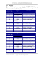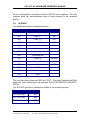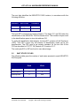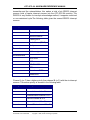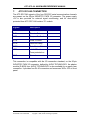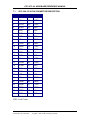
1
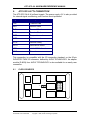
ATC-SCC-04 Quad Channel Serial Communication Controller RS-232 / 422 / 485 / TTL Industry Pack Module REFERENCE MANUAL 773-12-000-4000 Revision 1.2 April 2003 ALPHI TECHNOLOGY CORPORATION 6202 S. Maple Avenue #120 Tempe, AZ 85283 USA Tel: (480) 838-2428 Fax: (480) 838-4477 ATC-SCC-04 HARDWARE REFERENCE MANUAL NOTICE The information in this document has been carefully checked and is believed to be entirely reliable. While all reasonable efforts to ensure accuracy have been taken in the preparation of this manual, ALPHI TECHNOLOGY assumes no responsibility resulting from omissions or errors in this manual, or from the use of information contain herein. ALPHI TECHNOLOGY reserves the right to make any changes, without notice, to this or any of ALPHI TECHNOLOGY’s products to improve reliability, performance, function or design. ALPHI TECHNOLOGY does not assume any liability arising out of the application or use of any product or circuit described herein; nor does ALPHI TECHNOLOGY convey any license under its patent rights or the rights of others. ALPHI TECHNOLOGY CORPORATION All Rights Reserved This document shall not be duplicated, nor its contents used for any purpose, unless express permission has been granted in advance. ALPHI TECHNOLOGY CORP. Part Number: 753-12-000-4000 Page ii Copyright 2000, ALPHI Technology Corporation REV 1.22 ATC-SCC-04 HARDWARE REFERENCE MANUAL TABLE OF CONTENTS 1. INTRODUCTION ___________________________________________ 4 2. SUMMARY OF FEATURES __________________________________ 5 3. DESCRIPTION_____________________________________________ 6 3.1 3.2 3.3 3.4 3.5 BLOCK DIAGRAM ______________________________________________________ INDUSTRY PACK SPACES _______________________________________________ I/O SPACE ____________________________________________________________ ID SPACE _____________________________________________________________ WAIT STATE CYCLES___________________________________________________ 4. ATC-SCC-04 CHARACTERISTICS____________________________ 10 5. ZILOG SCC Z85230 _______________________________________ 11 6 6 7 8 9 6. BAUD RATE GENERATOR _________________________________ 12 6.1 6.2 6.3 6.4 6.5 ASYNCHRONOUS MODE _______________________________________________ SYNCHRONOUS MODE ________________________________________________ DATA ENCODING _____________________________________________________ Z85230 INTERRUPT FUNCTION__________________________________________ Z8530 REGISTERS ACCESS ____________________________________________ 7. ATC-SCC-04A CONNECTION _______________________________ 17 7.1 SCC-04A: I/O 50 PIN CONNECTOR DESCRIPTION. _________________________ 18 8. ATC-SCC-04B CONNECTION _______________________________ 19 8.1 SCC-04B: I/O 50 PIN CONNECTOR DESCRIPTION. _________________________ 20 9. ATC-SCC-04-TTL CONNECTION _____________________________ 21 9.1 CLOCK SOURCES_____________________________________________________ 21 9.2 SCC-04TTL: I/O 50 PIN CONNECTOR DESCRIPTION. _______________________ 23 10. ADENDUM TO MANUAL ___________________________________ 24 ALPHI TECHNOLOGY CORP. Part Number: 753-12-000-4000 Page iii Copyright 2000, ALPHI Technology Corporation 12 13 14 14 16 REV 1.22 ATC-SCC-04 HARDWARE REFERENCE MANUAL 1. INTRODUCTION The ATC-ATC-SCC-04 module from ALPHI TECHNOLOGY is a Serial Communication Controller based on the Zilog 85230 SCC and is implemented on a single wide Industry Pack according to the INDUSTRY PACK VITA 4 specification. Two types are available: Reference Description ATC-SCC-04A Four RS-232C serial channels ATC-SCC-04B Four RS-422/RS-485 serial channels ATC-SCC-04-ttl Four ttl level serial channels –20 to +85 temperature grade version is available as a opt. -I ATC-SCC-04 Industry Pack provides four asychronous or synchronous fullduplex serial channels, with an seperate baud rate generator for each channel. An on-board non-volatile EEPROM maintains ATC-SCC-04 identification codes and provides additional user space. ALPHI TECHNOLOGY CORP. Part Number: 753-12-000-4000 Page 4 Copyright 2000, ALPHI Technology Corporation REV 1.22 ATC-SCC-04 HARDWARE REFERENCE MANUAL 2. SUMMARY OF FEATURES • Single-size INDUSTRY PACK module. • Four asynchronous and synchronous full-duplex serial channels. • Fully compatible with the VITA 4 INDUSTRY PACK specification. • RS-232 interface- ATC-SCC-04A • RS-422/485 interface- ATC-SCC-04B • TTL interface- ATC-SCC-ttl • 4-Byte transmitter FIFO and the 8-Byte receiver FIFO • Status FIFO anti-lock feature in DMA-driven system • Separate baud rate generator for each channel. • Data rate up to: 115 kbaud in async. mode, 2 Mbaud in synchronous mode. • Supports multi-drop 2-wire configuration ATC-SCC-04B with driver output enable through /RTS signal. • Zilog SCC Z85230 controller. • 5 V only power supply. • Extended temperature grade available (-40 to +85 °C). ALPHI TECHNOLOGY CORP. Part Number: 753-12-000-4000 Page 5 Copyright 2000, ALPHI Technology Corporation REV 1.22 ATC-SCC-04 HARDWARE REFERENCE MANUAL 3. DESCRIPTION The ATC-SCC-04 is based on the Serial Communication Controller (SCC) Z85230 from Zilog. Each Z85230 provides two full-duplex ports for asynchronous and synchronous communication. The transmitter has an 8-bit transmit data register loaded from the internal data bus and a shift register loaded from the transmit data register. The receiver has a 4/8-Byte data FIFO with an 8-bit error FIFO, and a 8-bit shift register. This arrangement reduces CPU time overhead. The Z85230 interrupt structure supports vectorized or nonvectorized interrupts. The ATC-SCC-04A module provides superior performance, for multiple serial channels. Data transmission and reception are performed independently on each channel with five to eight data bits per character, plus optional even or odd parity. The transmitter can supply one, one and a half, or two stop bits per character. The full modem control signals of the four independent channels are available on the 50-pin INDUSTRY PACK I/O connector. The ATC-SCC-04B module provides four RS-422/485 channels. It is especially oriented for high speed synchronous communications and allows the connection of up 32 transmitters and receivers to a single multi drop bus (2wire). 3.1 BLOCK DIAGRAM There are four basic section to the ATC-SCC-04: • The INDUSTRY PACK bus interface. • The Z85230 controllers. • The serial communication physical interface: RS-232C for the ATC-SCC-04A, or RS-422/RS-485 for the ATC-SCC-04B, ATC-SCC-04-ttl. • The 2 kByte of non-volatile memory. 3.2 INDUSTRY PACK SPACES The following table gives the four ATC-SCC-04 memory spaces. • ID space INDUSTRY PACK identification codes • I/O space CIO controllers access • INT Ack Interrupt acknowledge The base address of these spaces depends on the specific INDUSTRY PACK carrier used . ALPHI TECHNOLOGY CORP. Part Number: 753-12-000-4000 Page 6 Copyright 2000, ALPHI Technology Corporation REV 1.22 ATC-SCC-04 HARDWARE REFERENCE MANUAL 3.3 I/O SPACE The two Z85230 controllers are mapped into the INDUSTRY PACK I/O space. Data and command registers of the Z85230 controllers are placed on 8 consecutive addresses (8-bit data path). DSP Carrier I/O space addr. Register Description Z85230 (0) controller $0 CBCR Channel B Command Register $1 CBDR Channel B Data Register $2 CACR Channel A Command Register $3 CADR Channel A Data Register Z85230 (1) controller $4 CDCR Channel D Command Register $5 CDDR Channel D Data Register $6 CCCR Channel C Command Register $7 CCDR Channel C Data Register $10 85230 CLK Slave Carrier I/O space addr. Register 0 = 8Mhz / 1 = 16Mhz Description Z85230 (0) controller $0 CBCR Channel B Command Register $4 CBDR Channel B Data Register $8 CACR Channel A Command Register $C CADR Channel A Data Register Z85230 (1) controller $10 CDCR Channel D Command Register $14 CDDR Channel D Data Register $18 CCCR Channel C Command Register $1C CCDR Channel C Data Register $40 85230 CLK ALPHI TECHNOLOGY CORP. Part Number: 753-12-000-4000 0 = 8Mhz / 1 = 16Mhz Page 7 Copyright 2000, ALPHI Technology Corporation REV 1.22 ATC-SCC-04 HARDWARE REFERENCE MANUAL All port configurations are defined with the Z85230 control registers. The data registers allow the transmit/receive data of each channels to be accessed directly. 3.4 ID SPACE The identification space is defined as follows: ID space addr. Description value $01 Ascii "I" $49 $03 Ascii "P" $50 $05 Ascii "A" $41 $07 Ascii "C" $43 $09 Manufacturer identification $11 $0B Module type $0D Revision module $0F Reserved $00 $11 Driver ID low byte $13 Driver ID high byte $15 Number of bytes used $0C $17 CRC $3F- user $19 user The four first bytes contain the ASCII text "IPAC". This clearly identifies the ROM beginning. The manufacturer code identifies ALPHI TECHNOLOGY INDUSTRY PACKs. The ATC-SCC-04 device is defined as follows by the module type byte. Module Module type byte ATC-SCC-04A $04 ATC-SCC-04B $05 ATC-SCC-04-ttl $09 ALPHI TECHNOLOGY CORP. Part Number: 753-12-000-4000 Page 8 Copyright 2000, ALPHI Technology Corporation REV 1.22 ATC-SCC-04 HARDWARE REFERENCE MANUAL The next byte identifies the INDUSTRY PACK revision, in accordance with the following definition. Revision ASCII char. hex value first "_" (space) $5F next "A" "B" ... $41 $42 The byte $0F is reserved for future extension. The bytes $11 and $13 allow the identification of the INDUSTRY PACK software driver. The number of bytes used in the identification space is stored at address $15. To verify the identification data integrity, the byte $17 contains a 8-bit Checksum (CRC). This CRC covers only the number of identification codes set by the manufacturer. The CRC used is an industry standard. It's the low 8-bit of the FCS as described in CCITT T.30 (Fascicle VII.3) section 5.3.7. The next bytes $19 to $3F are free for user data storage. 3.5 WAIT STATE CYCLES The following table gives the number of wait states asserted in each INDUSTRY PACKs space. Space Wait state Wait state Read Write I/O 2 2 Identification 2 2 Interrupt ack. 6 N/A ALPHI TECHNOLOGY CORP. Part Number: 753-12-000-4000 Page 9 Copyright 2000, ALPHI Technology Corporation REV 1.22 ATC-SCC-04 HARDWARE REFERENCE MANUAL 4. ATC-SCC-04 CHARACTERISTICS Symbol Parameters Test Max Unit BR Baud rate Asynchronous 115 kBaud BR Baud rate Synchronous 2 MBaud ICC Vcc current 670 PCLK Peripheral clock 8 ATC-SCC-04 (commercial) 0 to +70 °C ATC-SCC-04X (industrial) -40 to +85 °C Tstg Storage temperature -60 to 150 °C ALPHI TECHNOLOGY CORP. Part Number: 753-12-000-4000 Page 10 Copyright 2000, ALPHI Technology Corporation mA MHz REV 1.22 ATC-SCC-04 HARDWARE REFERENCE MANUAL 5. ZILOG SCC Z85230 The ATC-SCC-04 INDUSTRY PACK contains two NMOS Z8530 devices, and the following description gives you the features of these Z85230 controllers. Each Z8530 device provides two full-duplex serial channels for multiprotocol asynchronous and synchronous transmission modes. The Z85230 handles asynchronous formats, synchronous byte-oriented protocols such as IBM ® Bisync, and synchronous bit-oriented protocol such as HDLC and IBM ® SDLC. This versatile device supports virtually any serial data transfer application. The Z85230 can generate and check CRC codes in any synchronous mode and can be programmed to check data integrity in various modes. The device also has facilities for modem control in both channels. Each Z85230 channel provides a receiver FIFO of 8 Bytes deep, and a transmitter FIFO of 4 byte deep. Each Z85230 controller provides an interrupt connected to IRQ0 and IRQ1 of the INDUSTRY PACK logic interface respectively. ALPHI TECHNOLOGY CORP. Part Number: 753-12-000-4000 Page 11 Copyright 2000, ALPHI Technology Corporation REV 1.22 ATC-SCC-04 HARDWARE REFERENCE MANUAL 6. BAUD RATE GENERATOR The Z85230 provides a baud rate generator for each channel, consisting of one16-bit time-constant register, a 16-bit down-counter, and a flip-flop on the output that makes the output a square wave. The down-counter clock is divided by the clock mode value, and the clock mode source allows to select the master clock between the system clock PCLK and the input pin RTxC On startup, the value in the time constant-register is loaded into the counter, and the counter begins counting down. When a count of zero is reached, the output of the baud rate generator toggles, the time-constant value is loaded into the counter, and the process repeats. In asynchrounous mode, two clock sources are available: PCLK pin (8 MHz) with clock mode equal to 16, 32 or 64, or RTxC pin (2.4576 MHz) with clock mode equal to 1. In synchronous mode (ATC-SCC-04B and ATC-SCC-04C modules) - RTxC pin (Receive clock line) is the clock source -, the clock mode selection is always equal to 1. The mode clock value representes the frequency ratio between the data rate output and the frequency sample of the received character. The following formula allows to define the desired baud rate output: 6.1 ASYNCHRONOUS MODE In this transmission mode, an asynchronous message format is defined as follows: • A start bit • The data field • The parity bit • Stop bit(s) The start bit indicates the beginning of the character transmission. The data field contains the character to be transmited, and the number of bits per character can be set from 5 to 8. The parity bit generation and checking is optional. For even parity, the parity bit is set when the data bits plus the parity bit contain an even number of 1s. For odd parity, the parity bit is set when the data bits plus the parity bit contain an odd number of 1s. The stop bit(s) signal(s) the end of transmit character, and provide(s) a minimum interval between two emission characters. The available number of stop bit is one, one and a half, and two. There are four modem control signals, associated with the transmitter, provided by the Z85230: /RTS, /CTS, /DTR and /DCD. When the auto enable function is set (for more information, refer to the Zilog Z85230 User's manual), the /RTS ALPHI TECHNOLOGY CORP. Part Number: 753-12-000-4000 Page 12 Copyright 2000, ALPHI Technology Corporation REV 1.22 ATC-SCC-04 HARDWARE REFERENCE MANUAL signal remains low until the transmitter is completely empty and the last stop bit has left the TxD pin. The /CTS line becomes active when the transmitter is enabled. The /DCD line becomes active when the receiver is enabled. The /DTR signal goes low to indicate the terminal ready state, and goes high when the transmit is reseted. If these control functions are not required, these pins can be used as general-purpose I/O signals. The receive data path provides an error FIFO in parallel with the data FIFO. Three error conditions that the receiver checks in asynchronous mode are: • Framing error - when the data length is too long. • Parity error - The parity bit disagrees with the programmed sens. • Overrun errors - When the receive FIFO overflows. 6.2 SYNCHRONOUS MODE The synchronous versus asynchronous communication requires a common clock signal reference to both transmitter and receiver. This solution eliminates the overhead associated with every character (start and stop bits in asynchronous mode) and increases the line efficiency. In the receiver data path, the mode clock must be equal to one that allows higher speed communication links. Some applications may encode the clock information on the same line as the data. Because of the phase relationship of synchronous data to a clock, data is transferred in blocks with no gaps between characters. A synchronization pattern (6-bit, 8-bit, or 16-bit length) is normally used to indicate the location of a block transmission. For example monosync protocol usually uses $16 as this special character, and the SDLC protocol uses the $7E character to mark the beginning and the end of a block of data. The Z85230 supports the three following byteoriented protocols: monosynchronous, bisynchronous, and external synchronous The Z85230 offers several options to support synchronous mode including various sync generation and checking, CRC generation and checking, as well as modem controls, and a transmitter to receiver synchronization function. In synchronous communication the number of bits per character can be set between five, six, seven, or eight. An additional - odd or even - parity bit can be carried for each transmit character. Typically the parity bit is not used in synchronous applications because the CRC provides a more reliable method for detecting errors. Either the CRC-16 polynomial or the CRC-CCITT polynomial may be used to check the data integrity. The modem control signals /RTS and /CTS, in synchronous transmission, are used as simple I/O pin. Note: On the ATC-SCC-04B, the /RTS signal controls the output enable driver of the RS-422/RS-485 serial interface. In this way, before each transmission, the /RTS signal must be set to low, and automatically return to the high state at the end of the complete block transmission to insure no collision. ALPHI TECHNOLOGY CORP. Part Number: 753-12-000-4000 Page 13 Copyright 2000, ALPHI Technology Corporation REV 1.22 ATC-SCC-04 HARDWARE REFERENCE MANUAL In bit-oriented protocol (Synchronous Data Link Control mode, SDLC), the synchronization character is similar to bisync and monosync modes. High level Data Link Control (HDLC) is defined as CCITT, also EIAJ standards: SDLC is one of the implementation made by IBM ® . Frames of information are enclosed by a unique bit pattern called a flag, usually equal at $7E. The basic format of an SDLC/HDLC frame is described as following: • A 8-bit flag character ($7E), to mark the frame beginning. • A 8-bit address field, it is used to designed receiving stations. • A 8-bit control field. • The data information field. • A 16-bit frame checking field, in SDLC mode only the CRC-CCITT is used. • A 8-bit flag character ($7E), to mark the frame ending. 6.3 DATA ENCODING Four data encoding capabilities are provided by the Z85230 to allow the transmit of the data information and the clock transmission one the same line. • NRZ (Non-Return to Zero), encoding a 1 is represented by a high level and a 0 is represented by a low level. • NRZI (Non-Return to Zero Inverted), encoding a 1 is represented by no change in the level and a 0 is represented by a change in the level. • FM1 (biphase mark), a transition is present on every transmit bit, encoding a 1 is represented by an additional transition presents in the bit middle, the 0 state contains no transition in the bit middle. The FM1 encoded data contains sufficient information to recover a clock from the data. • FM0 (biphase space), the encoding method is the same that FM1, but the 1 is represented such as a 0 in FM1 encoding, also the 0 level is encoded such as the 1 in FM1. Each Z85230 channel contains a Digital Phase-Locked Loop (DPLL) that can be used to recover the clock information from the received data with NRZ, NRZI, FM1 and FM0 encoding. 6.4 Z85230 INTERRUPT FUNCTION The Z85230 operations must be controlled by polling or interrupt modes. In polling mode, the Z85230 transmitter/receiver status is show by a continuous reading into the Z85230 status registers (for more information, refer to the Zilog Z85230 User's maual). The interrupt mode reduces the CPU overhead system. Three Z85230 sources can generate an interrupt request: the receiver, the ALPHI TECHNOLOGY CORP. Part Number: 753-12-000-4000 Page 14 Copyright 2000, ALPHI Technology Corporation REV 1.22 ATC-SCC-04 HARDWARE REFERENCE MANUAL transmitter and the external/status, this makes a total of six Z85230 interrupt sources (total of twelve interrupt sources into the ATC-SCC-04 module). The Z85230 is very flexible for interrupt acknowledge method, it supports vectorized or non-vectorized cycle.The following table gives the several Z85230 interrupt sources. Interrupt source Condition Receiver Character available Receive overrun Framing error End of frame (SDLC) Parity error Transmitter Buffer empty External/Status Zero count DCD SYNC/HUNT CTS Tx underrun/EOM Break/Abort Channel A (or C) has a higher priority than channel B (or D) with the six interrupt sources. This source priority is showed in the following table. Priority level Interrupt source Highest Receive channel A or C Transmit channel A or C External/Status channel A or C Receive channel B or D Transmit channel B or D Lowest External/Status channel B or D ALPHI TECHNOLOGY CORP. Part Number: 753-12-000-4000 Page 15 Copyright 2000, ALPHI Technology Corporation REV 1.22 ATC-SCC-04 HARDWARE REFERENCE MANUAL The hardware daisy-chain operation is not implemented, because each CIOcontroller has its own interrupt request line into the INDUSTRY PACK logic interface. In the ATC-SCC-04 module, the Z85230(0) interrupt line is connected to the /IRQ0, and the Z85230(1) interrupt line is connected to the /IRQ1 signal on the INDUSTRY PACK logic interface. 6.5 Z8530 REGISTERS ACCESS Two cycles are necessary to address an internal register, as the internal Z85230 registers are accessed through an internal pointer register. The first cycle is the write pointer operation, into the Write Register 0 which selects the internal register. The next cycle is the data access operation. The following state machine shows the internal register operation. The state 0 waits for the pointer writing (in the Write Register 0) which selects the internal register selection. After the data access (read or write cycle), the state machine returns to the state 0, waiting for the next pointer writing. A minimum time of 500 ns is required between the pointer writing and the data access operation. All internal CIO registers, including the internal data register, are accessed through this method. The pointer register is automatically cleared after each following read or write cycle. For more details on register programming and Z85230 functionalities, please refer to the Zilog "Z85230 User's manual". ALPHI TECHNOLOGY CORP. Part Number: 753-12-000-4000 Page 16 Copyright 2000, ALPHI Technology Corporation REV 1.22 ATC-SCC-04 HARDWARE REFERENCE MANUAL 7. ATC-SCC-04A CONNECTION The ATC-SCC-04A signals of the four RS-232C serial communication channels are present on the 50-pin INDUSTRY PACK I/O connector. The power supply +5V is also provided for external signal conditioning, and it's short-circuit protected from ATC-SCC-04A revision "A" module. Signals Description TxD Transmit Data RxD Receive Data /RTS Request To Send /CTS Clear To Send /DTR Data Set Ready /DCD Data Carrier Detect VDD + 5 V 500 mA max. Fuse protected on GND Ground This connection is compatible with the I/O connection standard, on the 50-pin INDUSTRY PACK I/O connector, defined by ALPHI TECHNOLOGY. An adaptor module (RJ45Q) from ALPHI TECHNOLOGY is also available for an easily user connection. It provides four RJ-45 connectors and measures 3HE x 4TE on front panel. ALPHI TECHNOLOGY CORP. Part Number: 753-12-000-4000 Page 17 Copyright 2000, ALPHI Technology Corporation REV 1.22 ATC-SCC-04 HARDWARE REFERENCE MANUAL 7.1 SCC-04A: I/O 50 PIN CONNECTOR DESCRIPTION. PIN SIGNAL PIN SIGNAL 1 GND 26 GND 2 NC 27 DCDC 3 DCDA 28 RTSC 4 RTSA 29 GND 5 GND 30 GND 6 GND 31 NC 7 VDD 32 VDD 8 NC 33 TXDC 9 TXDA 34 RXDC 10 RXDA 35 CTSC 11 CTSA 36 DTRC 12 DTRA 37 NC 13 GND 38 GND 14 NC 39 DCDD 15 DCDB 40 RTSD 16 RTSB 41 GND 17 GND 42 GND 18 GND 43 NC 19 VDD 44 VDD 20 NC 45 TXDD 21 TXDB 46 RXDD 22 RXDB 47 CTSD 23 CTSB 48 DTRD 24 DTRB 49 NC 25 GND 50 GND Note: NC: No Connect VDD: 5 volt Fused ALPHI TECHNOLOGY CORP. Part Number: 753-12-000-4000 Page 18 Copyright 2000, ALPHI Technology Corporation REV 1.22 ATC-SCC-04 HARDWARE REFERENCE MANUAL 8. ATC-SCC-04B CONNECTION The ATC-SCC-04B/C differential signals of the four RS-422 / RS-485 serial communication channels are present on the 50-pin INDUSTRY PACK I/O connector. The power supply +5V is also provided for external signal conditioning, and it's short-circuit protected from ATC-SCC-04B/C revision "A" module. Signals Description TxD± Transmit Data RxD± Receive Data TxC± Transmit Clock RxC± Receive Clock VDD + 5 V 500mA Fuse protected GND Ground This connection is compatible with the I/O connection standard, on the 50-pin INDUSTRY PACK I/O connector, defined by ALPHI TECHNOLOGY. An adapter module (RJ45Q) from ALPHI TECHNOLOGY is also available for an easily user connection. ALPHI TECHNOLOGY CORP. Part Number: 753-12-000-4000 Page 19 Copyright 2000, ALPHI Technology Corporation REV 1.22 ATC-SCC-04 HARDWARE REFERENCE MANUAL 8.1 SCC-04B: I/O 50 PIN CONNECTOR DESCRIPTION. PIN SIGNAL PIN SIGNAL 1 GND 26 GND 2 NC 27 TXDC+ 3 TXDA+ 28 TXDC- 4 TXDA- 29 RXDC+ 5 RXDA+ 30 RXDC- 6 RXDA- 31 NC 7 +5VF 32 +5VF 8 NC 33 TXCC+ 9 TXCA+ 34 TXCC- 10 TXCA- 35 RXCC+ 11 RXCA+ 36 RXCC- 12 RXCA- 37 NC 13 GND 38 GND 14 NC 39 TXDD+ 15 TXDB+ 40 TXDD- 16 TXDB- 41 RXDD+ 17 RXDB+ 42 RXDD- 18 RXDB- 43 NC 19 +5VF 44 +5VF 20 NC 45 TXCD+ 21 TXCB+ 46 TXCD- 22 TXCB- 47 RXCD+ 23 RXCB+ 48 RXCD- 24 RXCB- 49 NC 25 GND 50 GND Note: NC: No Connect +5VF: 5 volt Fused ALPHI TECHNOLOGY CORP. Part Number: 753-12-000-4000 Page 20 Copyright 2000, ALPHI Technology Corporation REV 1.22 ATC-SCC-04 HARDWARE REFERENCE MANUAL 9. ATC-SCC-04-TTL CONNECTION The ATC-SCC-04-ttl ttl buffered signals. The power supply +5V is also provided for external signal conditioning, and it's short-circuit protected. Signals Description TxD Transmit Data RxD Receive Data TxC± Transmit Clock RxC± Receive Clock /RTS Request to send /CTS Clear to send /DTR Data set ready /DCD Data carrier detect VDD + 5 V 500Ma fused GND Ground This connection is compatible with the I/O connection standard, on the 50-pin INDUSTRY PACK I/O connector, defined by ALPHI TECHNOLOGY. An adapter module (RJ45Q) from ALPHI TECHNOLOGY is also available for an easily user connection. 9.1 CLOCK SOURCES 3 2 1 J4 1 J3 J5 J2 J1 ALPHI TECHNOLOGY CORP. Part Number: 753-12-000-4000 Page 21 Copyright 2000, ALPHI Technology Corporation REV 1.22 ATC-SCC-04 HARDWARE REFERENCE MANUAL J1, J2, J3, J4 Clock source for RTxC • Pin 1 to 2 jumpered is for external clock on P2 • Pin 2 to 3 jumpered Internal clock J5 Clock source for TRxC • Pin 1 to 2 jumpered is for input clock • Pin 2 to 3 jumpered is for output clock ALPHI TECHNOLOGY CORP. Part Number: 753-12-000-4000 Page 22 Copyright 2000, ALPHI Technology Corporation REV 1.22 ATC-SCC-04 HARDWARE REFERENCE MANUAL 9.2 SCC-04TTL: I/O 50 PIN CONNECTOR DESCRIPTION. PIN SIGNAL PIN SIGNAL 1 GND 26 GND 2 NC 27 /DCDc 3 /DCDa 28 /RTSc 4 /RTSa 29 TXCc 5 TXCa 30 RXCc 6 RXCa 31 +12V 7 Vdd 32 Vdd 8 +12V 33 TXDc 9 TXDa 34 RXDc 10 RXDa 35 /CTSc 11 /CTSa 36 /DTRc 12 /DTRa 37 NC 13 GND 38 GND 14 NC 39 /DCDd 15 /DCDb 40 /RTSd 16 /RTSb 41 TXCD 17 TXCb 42 RXCd 18 RXCb 43 VDD 19 VDD 44 -12V 20 -12V 45 TXDd 21 TXDd 46 RXDd 22 RXDb 47 /CTSd 23 /CTSb 48 /DTRd 24 /DTRb 49 NC 25 GND 50 GND NC: No Connect ALPHI TECHNOLOGY CORP. Part Number: 753-12-000-4000 Page 23 Copyright 2000, ALPHI Technology Corporation REV 1.22 ATC-SCC-04 HARDWARE REFERENCE MANUAL 10. ADENDUM TO MANUAL This product has been modified in the Altera code to work with an IP-CLK of 8Mhz or 32Mhz by adding a control register accessed on the I/O space address $10 of DSP carrier or $40 of a slave carrier board. The register controls the clock speed of the 85230 on board. The 85230’s are either 16Mhz or 20Mhz so they can only run at 8Mhz or 16Mhz, there is a 32Mhz condition with this register that cannot be used. A table below we show each condition . CONTROL REGISTER (Read/Write) Address ($10 with Alphi DSP carrier) and ($40 with slave carrier) IPCLK REGISTER $10 WRITE 85230-PCLK INPUT CONDITION 8Mhz 0 8Mhz RD/WR 240ns 8Mhz 1 4Mhz N/A 32Mhz 0 32Mhz N/A 32Mhz 1 16Mhz RD/WR 60ns ALPHI TECHNOLOGY CORP. Part Number: 753-12-000-4000 Page 24 Copyright 2000, ALPHI Technology Corporation REV 1.22