1
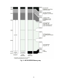
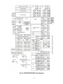
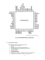
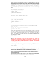
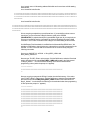
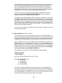
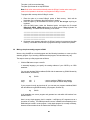
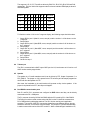
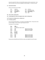
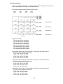
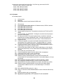
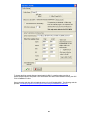
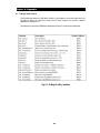
MiniDragon-Plus2 Trainer
For Freescale HCS12 microcontroller family
User’s Manual
Revision 1.03
Table OF Contents
Chapter 1. Introduction...........................................................................................................................4
1.1 Welcome....................................................................................................................................4
1.2 MC9S12DG256 features and memory map..........................................................................5
1.3 On-board hardware features ..................................................................................................8
1.4 I/O pin usage .............................................................................................................................9
Chapter 2. Quick Start ............................................................................................................................. 12
2.1 Install software from CD ...................................................................................................... 12
2.2 Getting Started ...................................................................................................................... 13
2.3 Test hardware ........................................................................................................................ 15
Chapter 3. Software Desriptions .........................................................................................................16
3.1 Bootloader and D-BUG12 monitor ..................................................................................... 16
3.1.1 EVB mode .................................................................................................................. 16
3.1.2 Jump to EEPROM mode.......................................................................................... 17
3.2.3 BDM POD mode ........................................................................................................ 17
3.2.4 Bootloader mode ...................................................................................................... 20
3.2 Making a simple assembly program in RAM.................................................................... 21
3.3 Software development ......................................................................................................... 23
Chapter 4. Hardware Descriptions......................................................................................................25
4.1 Power LED............................................................................................................................. 25
4.2 Jumper switches and pushbuttons .................................................................................. 25
4.3 Seven-Segment LED display.............................................................................................. 25
4.4 Trimmer pot........................................................................................................................... 25
4.5 Speaker.................................................................................................................................. 26
4.6 Dual RS232 communication ports .................................................................................... 26
4.7 External SPI interface .......................................................................................................... 27
4.8 Servo motor controllers...................................................................................................... 27
4.9 Dual H-Bridge for DC motor and Stepper motor controllers ........................................ 27
2
4.10 Temperature sensor ........................................................................................................... 27
4.11 LCD display module ........................................................................................................... 27
4.12 Keypad ................................................................................................................................. 28
4.13 All jumper settings.............................................................................................................. 29
Chapter 5. EmbeddedGNU..................................................................................................................30
Chapter 6. Code Warrior and serial monitor.....................................................................................32
Chapter 7. PLL code.............................................................................................................................33
Chapter 8. Appendix ............................................................................................................................34
8.1
D-Bug12 utility routines ..................................................................................................... 34
8.2
Interrupt vector tables ........................................................................................................ 35
8.3
Useful web links ................................................................................................................. 38
8.4
Troubleshooting notes....................................................................................................... 38
3
Chapter 1. Introduction
1.1
Welcome
Thank you very much for purchasing the MiniDragon-Plus2 trainer. The MiniDragon-Plus2 trainer
is a low-cost, feature-packed training board for the Freescale HCS12 microcontroller family. It is
compatible with the Freescale 9S12DP256EVB board and other similar development boards on
the market today, but it also incorporates many on-board peripherals that make this board one of
the best trainers in universities around the world.
For engineers, it is a convenient prototype system suitable for designers who want to rapidly
develop and prototype new HCS12 applications. For students, it can not only to be used as a
general trainer for freshman and sophomore students, but also as a powerful platform for senior
projects as well. The compact size and new features of the MiniDragon-Plus2 board create a new
potential for students at every level.
The MiniDragon-Plus2 trainer kit comes with the following items:
1. MiniDragon-Plus2 board
2. CD ROM which contains:
a. AsmIDE with HCS12 assembler
b. Sample programs with source code
c. Freescale application notes for the HCS12
d. Data sheets for on-board hardware
e. User’s manual
f. Reference documents
3. RS232 cord
4. 110V AC adapter for North America customers
If you miss any part of the kit, please contact [email protected] or call 630 894-1440 for help.
The specification of the AC adapter is:
DC input:
DC output:
Current rating:
Type of plug:
110V
7.5V-9V
300mA
2.1mm female barrier plug, center positive
The AC adapter is only available to North American customers.
WARNING: If more power is needed in some applications, you should upgrade the AC adapter.
Otherwise, the board could keep resetting itself when the VCC drops below 4.6V.
If your board sometimes resets by itself you need to upgrade your AC adapter to 9VDC
output at 800mA or at 1A. Do not use an AC adapter whose DC output voltage is rated
higher than 9V with this board. If an AC adapter is rated for 9V at 300mA it should have
an output DC voltage about 12.5V without a load, 9V with a full load.
4
1.2
MC9S12DG256 features and memory map:
The MiniDragon-Plus2 board may come with theMC9S12DP256CCPV or the
MC9S12DG256CVPE installed. The MC9S12DG256 is the best replacement for the
MC9S12DP256 since the latter has been discontinued by Freescale. The only difference
between DG256 and DP256 is the number of CAN ports. The DG256 has 2 CAN ports, but the
DP256 has 5 CAN ports. Other than the different number of CAN port these two microcontrollers
have the same features. If you don't use more than 2 CAN ports these two chips are identical
and all datasheets and manuals for the DP256 can be used for the DG256.
The MC9S12DG256 microcontroller consists of a powerful 16-bit CPU (central processing unit),
256K bytes of flash memory, 12K bytes of RAM, 4K bytes of EEPROM and many on-chip
peripherals.
The main features of the MC9S12DG256 are listed below:
•
•
•
•
•
•
•
•
•
•
•
•
•
•
Powerful 16-bit CPU
256K bytes of flash memory
12K bytes of RAM
4K bytes of EEPROM
SCI ports
SPI ports
CAN 2.0 ports
I2C interface
8-ch 16-bit timers
8-ch 8-bit or 4-ch 16 bit PWM
16-channel 10-bit A/D converter
Fast 25 MHz bus speed via on-chip Phase Lock Loop
BDM for in-circuit programming and debugging
112-pin LQFP package offers up to 91 I/O in a small footprint
5
Fig 1-1: MC9S12DG256 Memory map
6
Fig 1-2: MC9S12DG256 MCU block diagram
7
Fig 1-3: MC9S12DG256 MCU pin assignments
1.3
On-board hardware features:
The MiniDragon-Plus2 board includes the following features:
1.
2.
3.
4.
5.
6.
7.
8.
9.
10.
Dual RS232 communication ports
CAN port
SPI expansion port for interfacing external SPI devices
Four robot servo controllers with terminal block for external 5V
7-segment LED display
Two jumper switches
Two push button switches
5V regulator with DC jack
Speaker to be driver by timer, or PWM signal for alarm or music applications.
Dual H-Bridge for controlling two DC motors or one Stepper motor
8
11.
12.
13.
14.
15.
16.
17.
18.
19.
20.
21.
22.
Power-On LED indicator
BDM-in connector to be connected with a BDM from multiple vendors for debugging
BDM POD mode for programming other HCS12 boards. No extra hardware needed
Abort switch for stopping program when program is hung in a dead loop
Mode switch for selecting 4 operating modes: EVB, Jump-to-EEPROM, BDM POD and
Bootloader
4 X 4 keypad header
Wytec’s TinyBee 3-axis accelerometer interface or GP2-D12 distance measuring sensor
interface for distance measurement
Potentiometer trimmer pot for analog input
Temperature sensor
Female or male headers provides all I/O pins of the MC9S12DG256
400-tie solderless breadboard included
Small PC board size is 5.25" X 3.40"
The MiniDragon-Plus2 board has the following features as options:
23.
24.
25.
26.
27.
28.
29.
1.4
RF transmitter
RF receiver
4 X 4 keypad
16X2 LCD
RTC
RS485 communication
Form C relay output rated at 3A/30V or 1A/125V
I/O Pin Usage
Many I/O pins of the MC9S12DG256 on the MiniDragon-Plus2 board are used by on-board
peripherals, but thanks for the large 112-pin LQFP package, there are still many I/O pins available
for your circuits on the breadboard. Also it’s unlikely that all on-board peripherals will be used by
one application program. So the I/O pins on unused peripheral devices can still be used by your
circuits on the breadboard. For instance, if you don’t connect a keypad, the entire port A will be
available to your circuits. If you don’t use LCD, the port K will be available as well. Port B drives
H-Bridge, but if you don’t connect a motor, the port B can drive any other I/O devices on the
breadboard.
9
Pin Name
Pin #
I/O Usage
PA0
PA1
PA2
PA3
PA4
PA5
PA6
PA7
Pin 57
Pin 58
Pin 59
Pin 60
Pin 61
Pin 62
Pin 63
Pin 64
Col_0 of keypad (output)
Col_1 of keypad (output)
Col_2 of keypad (output)
Col_3 of keypad (output)
Row_0 of keypad (input)
Row_1 of keypad (input)
Row_2 of keypad (input)
Row_3 of keypad (input)
PB0
PB1
PB2
PB3
PB4
PB5
PB6
PB7
Pin 24
Pin 25
Pin 26
Pin 27
Pin 28
Pin 29
Pin 30
Pin 31
H-bridge (output)
H-bridge (output)
H-bridge (output)
H-bridge (output)
not used
not used
not used
not used
PE0
PE1
PE2
PE3
PE4
PE5
PE6
PE7
Pin 56
Pin 55
Pin 54
Pin 53
Pin 39
Pin 38
Pin 37
Pin 36
Abort switch SW8 (input)
not used
not used
not used
not used
not used
not used
not used
PH0
PH1
PH2
PH3
PH4
PH5
PH6
PH7
Pin 52
Pin 51
Pin 50
Pin 49
Pin 35
Pin 34
Pin 33
Pin 32
Segment A on display
Segment B on display
Segment C on display
Segment D on display
Segment E on display
Segment F on display
Segment G on display
not used
PJ0
PJ1
PJ6
PJ7
Pin 22
Pin 21
Pin 99
Pin 98
not used
not used
not used
not used
PK0
PK1
PK2
PK3
PK4
PK5
PK7
Pin 8
Pin 7
Pin 6
Pin 5
Pin 20
Pin 19
Pin 108
RS of LCD module (output)
EN of LCD module (output)
DB4 of LCD module (output)
DB5 of LCD module (output)
DB6 of LCD module (output)
DB7 of LCD module (output)
not used
Table 1-1: I/O pin usage list 1
10
Pin Name
Pin #
I/O Usage
PM0
PM1
PM2
PM3
PM4
PM5
PM6
PM7
Pin 105
Pin 104
Pin 103
Pin 102
Pin 101
Pin 100
Pin 88
Pin 87
CAN0
CAN0
not used
not used
not used
not used
not used
I/O for external SPI (J10)
PP0
PP1
PP2
PP3
PP4
PP5
PP6
PP7
Pin 4
Pin 3
Pin 2
Pin 1
Pin 112
Pin 111
Pin 110
Pin 109
EN12 of H-bridge (output)
EN34 of H-bridge (output)
not used
not used
Servo motor 1 (output)
Servo motor 2 (output)
Servo motor 3 (output)
Servo motor 4 (output)
PS0
PS1
PS2
PS3
PS4
PS5
PS6
PS7
Pin 89
Pin 90
Pin 91
Pin 92
Pin 93
Pin 94
Pin 95
Pin 96
SCI0 for PC communication, RECV (RJ11 connector P1)
SCI0 for PC communication, XMIT (RJ11 connector P1)
SCI1 for user applications, RECV (RJ11 connector P2)
SCI1 for user applications, XMIT (RJ11 connector P2)
MISO for external SPI (J10)
MOSI for external SPI (J10)
SCLK for external SPI (J10)
I/O for external SPI (J10)
PT0
PT1
PT2
PT3
PT4
PT5
PT6
PT7
Pin 9
Pin 10
Pin 11
Pin 12
Pin 15
Pin 16
Pin 17
Pin 18
not used
not used
not used
not used
not used
Speaker (output)
BDMout reset (output, used in POD mode only)
BDMout data line (bi-directional, used in POD mode only)
PAD0
PAD1
PAD2
PAD3
PAD4
PAD5
PAD6
PAD7
Pin 67
Pin 69
Pin 71
Pin 73
Pin 75
Pin 77
Pin 79
Pin 81
D-bug12 mode select, S7
D-bug12 mode select, S7
Temperature sensor (U4, MCP9701A)
Pushbutton S2
Pushbutton S1
Jumper switch S3
Jumper switch S4
Trimmer pot VR1
PAD8
PAD9
PAD10
PAD11
PAD12
PAD13
PAD14
PAD15
Pin 68
Pin 70
Pin 72
Pin 74
Pin 76
Pin 78
Pin 80
Pin 82
X axis input for Wytec accelerometer module or ADC input for GP12D2
Y axis input for Wytec accelerometer module or ADC input for GP12D2
Z axis input for Wytec accelerometer module or ADC input for GP12D2
not used
not used
not used
not used
not used
Table 1-2: I/O pin usage list 2
11
Chapter 2. Quick Start
By default the MiniDragon-Plus2 board is pre-installed with the bootloader (Freescale AN2153.pdf) and
the D-Bug12 monitor (Freescale DB12RG4.pdf). In chapters 2 and 3 the AsmIDE is used as the main
software tool to develop and debug assembly programs. If you prefer to use Code Warrior IDE for C
program development and your board is pre-installed, per your request, with the serial monitor
(Freescale AN2548.pdf), skip the chapters 2 and 3 except clicking on the setup.bat in the CD to
install software .
People often use different terminologies. In our product manuals, Download means to transfer a file
from PC to a development board, while Upload means to transfer a file from a development board to
PC. Through out the manual, left click means that you click the left button of the mouse and right
click means that you click the right button of the mouse.
2.1
Install software from CD:
The installation is automated by double clicking on the SETUP.BAT in the CD. It will create a
folder c:\MiniDragonP2\examples and copy all example program files from the CD to
c:\MiniDragonP2\examples
If the filename is only shown as SETUP, not SETUP.BAT, you should change a folder option of
the Explorer to show file extension. When a file's extension is hiding, it is hard to know what it is.
To have your files to be shown with extensions, click on the TOOL tab in Explorer menu, then
click on folder options, then click on view tab, finally un-check the item named ‘Hide extensions
for knowing file types’.
The AsmIDE is free to use under GPL license. If you would like to use it in the future, we
encourage you donate $5.00 to Eric Engler at: http://www.ericengler.com/AsmIDE.aspx
After the software is successfully installed, you can make a shortcut to AsmIDE.exe on the
desktop. It’s important to make a shortcut so that its target location is C:\MiniDragonP2, not
c:\Windows\desktop or other locations. First, right click the Start button, then left click “Explorer”,
left click on C:\MiniDragonP2, right click on AsmIDE.exe (an application program), left click “Send
to” and finally left click “Desktop” (do not click “COPY”). It will create an icon named “shortcut to
AsmIDE” on the desktop and you can rename it to MiniDragon-Plus2. You can double check the
target location by right clicking on the icon, then left click on “properties”. You should see that the
target location is C:\MiniDragonP2. If you want to make a shortcut for AsmIDE on the Desktop,
this is the correct way to do it. If you don’t follow this method, you may have a problem running
your program. Never drag the AsmIDE.exe to the desktop folder.
The default setting of AsmIDE for the MiniDragon-Plus2 board is created in a text file named
c:\MiniDragonP2\AsmIDE.ini. In the future if you get lost with all the changes, you always can
copy this file into the folder c:\MiniDragonP2.
12
2.2
Getting Started
To operate the MiniDragon-Plus2 board, follow steps1 through 5 below:
1. Make sure that the two DIP switches of S7 must be set in the “low” positions for EVB mode,
then plug the AC adapter into a wall outlet, and plug the female plug of the AC adapter into
the DC jack on the left side of the MiniDragon Plus2 board. After power up, the speaker
should chirp once, the 7-segment LED should display a diagnostic code of E-4-3
momentarily. The letter E stands for EVB mode, the number 4 stands for single chip mode
and the number 3 means that 2 switches (S3, S4) are open. Here is the code explanation:
First letter: E = EVB mode, J = Jump to EEPROM, P = Pod and b = Bootloader mode.
Second number: 4 = Single chip mode, 6 = Narrow expended mode, 7 = Wide exp. mode
Third number: 0 = S3 & S4 closed, 1 = S3 open & S4 closed, 2 = S3 closed & S4 open 3=
S3 & S4 open
If a 16x2 LCD module is connected the LCD should display the following message:
“MiniDragon+2 EVB”
“D-Bug12 EVB MODE”
; you can display your name on LCD and see details
; at CDROM\examples\name_display\readme.txt
If it does not occur check the Power-On LED indicator. The PWR LED is the decimal point of
the 7-segment. It is lit when VCC (5V) is present. If the PWR LED is off check the J14 on
solder side. It should be shorted by a solder bridge. Also check the output of the AC adapter.
It should be about 10V DC without a load (the output DC voltage of the AC adapter is rated
for 7.5V at 300mA, but usually the voltage is much higher without a load).
2. Plug the RS232 cable into the RJ11 jack P1 at the left side of the MiniDragon Plus2 board
and plug the DB9 female end of the cable into COM1 or COM2 port on your PC. The RJ11
jack P2 on the top edge of the board is the MC9S12DG256’s SCI1 port that can be used by
a user’s program.
3. To invoke the AsmIDE, you can right click the Start button, then left click “Explorer”, left click
on C:\MiniDragonP2 and finally, double left click on AsmIDE.exe. If you have created a
shortcut icon on the desktop, just double click the AsmIDE icon on the desktop.
4. The AsmIDE is simple and very easy to use. You only need to use three commands from the
AsmIDE for your HCS12 development work. Use the File command to edit your source
code, the Build->Assemble command to assemble your source code, and the Build>Download command to download an s19 file to the MiniDragon-Plus2 board.
5. If your PC has a COM port output (it’s a 9-pin male DB9 connector), you don’t need a USB to
RS232 converter. Usually the PC COM port will be COM1 or COM2. For setting the COM
port of the AsmIDE, you can click through View-> Option->Terminal Window Options menu,
then select the correct COM port and skip the step 6.
13
6. If your PC does not have a COM port output, you have to use a USB to RS232 adapter, the
COM port number that the AsmIDE uses must match the USB-to-Serial COM port number
that is assigned by Windows O/S. Windows O/S assigns the USB-to-Serial COM port
number randomly and it does not know which COM port number that AsmIDE is going to
use. In order to find the USB-to-Serial COM port number, you can click through control panel
-> systems -> hardware -> device manager -> ports, the USB-to-Serial COM port number
will appear ( In Windows Vista, you left click on Start, right click on Computer, left click on
propriety, then Device Manager and then Continue ).
For setting the COM port of the AsmIDE to match that USB-to-Serial COM port number, you
can click through View-> Option->Terminal Window Options menu, then select the correct
COM port from COM1 to COM8.
7. Also, set the COM port options at 9600, N, 8,1, and check the “enable the terminal window”
box.
8. After reset, the D-Bug12 monitor defaults baud rate at 9600 and Hyperbaud function is
disabled. If Hyperbaud function is enabled, the Hyperbaud toolbar button sends the BAUD
57600 command to the D-Bug12 monitor, and then it also changes the serial port to the
57600 baud rate. IMPORTANT: When you reset your board it will go back to 9600 baud
and you will see characters ‘aaaaaaaaaa’ on the screen. You will need to press the
Hyperbaud button once to return AsmIDE to 9600 baud, and press it again to get 57600
baud. To stay at the 57600 baud all the time, you need to press the Hyperbaud button twice
after every reset. The Hyperbaud function is disabled by default and it should only be used
by an experienced user, not a beginner.
9. You can program text values for function keys to be sent from the terminal window. Some
function keys are pre-programmed, but you can change it any time in configuration options
(View->Options->Terminal Func Keys).
In the View->Option->Assembler menu, make sure that the chip family is 68HC12, not
68HC11. If you would like to use your own assembler, you can replace the as12.exe with the
name of your own assembler.
10. The screen is divided into two windows. The top window is for editing your source code and
the bottom window is shared by the message window and the terminal window.
If the terminal options are set correctly, you should see the following prompt every time the
reset button on the MiniDragon-Plus2 board is pressed. If you do not see this, the bottom
window may be set for message window. Sometime it’s a little confusing when terminal
window is disabled and the message window does not display what you have typed. In order
to enable terminal window you have to click the terminal button in the bottom window to
enable the terminal window display, then move the cursor to any location in the terminal
window and click the left button on the mouse. After seeing a solid block cursor flashes, press
the <Enter> key and it will enable the terminal window.
D-Bug12 v4.0.0b32
Copyright 1996 - 2005 Freescale Semiconductor
For Commands type "Help"
>
14
2.3
Test Hardware:
To help users get up and running, the MiniDragon-Plus2 board comes with many fully debugged,
some fairly advanced ready-to-run sample programs including source code, not just "Hello World"
type demo programs. The hardware test program, test.asm, simultaneously scans the keypad,
plays a song, changes 7-segment display brightness by adjusting the trimmer pot and vary music
playing tempo according to temperature change.
All sample programs must be run from RAM in EVB mode. In order to run the test program in
EVB mode, the two DIP switches of S7 must be set in the “low” positions to match the picture for
EVB mode.
The steps to run your first sample program are as follows:
1. Click the File button to open the test.asm from c:\MniDragonP2\examples. After the
test.asm is loaded into the top window, you can view instructions of how to test all
hardware on the MiniDragon-Plus2 board.
2. Click the Build button to assemble code and generate the test.s19 file. This is how you
normally generate an s19 file. You can omit this step, because the test.s19 is already on
your hard disk.
3. Press the reset button on the board, you will see:
D-Bug12 v4.0.0b32
Copyright 1996 - 2005 Freescale Semiconductor
For Commands type "Help"
>
4. Type “LOAD” <Enter>.
5. Click the Build button. Select Download option and locate the file ‘test.s19’ for
downloading. If it prompts you with the “save changes?” message, you can ignore that
message and click the “No” answer.
6. After download is done, type “G 2000” <Enter> to run the test program.
All sample programs on the CD are developed in RAM. You can try to run a different example
program later after you have finished reading this manual. You should always press the reset
button before downloading a new program, because the new program may not work if an
interrupt was enabled by a previous program.
All example programs are fully debugged, so the assembler won’t generate an error. If you have
an error, even a warning error, in your program, you must correct it before it can generate an s19
file.
15
Chapter 3. Software descriptions
3.1
Bootloader and D-Bug12 Monitor
The MC9S12DG256 on the MiniDragon-Plus2 board is pre-loaded with bootloader and D-Bug12
monitor firmware and it will operate in 4 different modes depending on the setting of the 2position DIP switch, S7. After power up or reset, the MC9S12DG256 will read the PAD0 and
PAD1 to decide which mode to boot up.
The bootloader (AN2153.PDF), the D-Bug12 reference guide (DB12RG4.PDF) and the
MC9S12DG256 data book (MC9SDG256.PDF) are the most important documentation. They
can be found on the folder named C:\MiniDragonP2\document after software installation. The
HCS12 instruction set, register map and memory map can be found on page 26, 65 and 120 of
the data book, respectively.
The new D-Bug12 V4.x is much different and much larger (about 60K) than old D-Bug12 V2.x.
The $C000-$EFFF are just a part of the monitor, In 16-bit S1 record they are $C000-$EFFF. In
24-bit S2 record, they are $FC000-FEFFF (ppage=$3F). Since the ppage register deals with the
16K window $8000-$BFFF the addresses $C000-$FFFF are not affected by the ppage. The
other part of the monitor is at C0000-C87FF (16K window $8000-$BFFF when ppage=$30,$31
and $32). See details on page 20 of the app note AN2153 or page 71 of the D-Bug12 v4
reference guide on the CD.
3.1.1 EVB mode: PAD1=0, PAD0=0.
This is the standard debug environment running on the MC9S12DG256 for on-chip RAM
or EEPROM based code development. Using an IDE program to view and modify
registers and memory locations, you may set breakpoints, single step through programs,
and assemble and disassemble code as you would in a BUFFALO monitor based
Freescale 68HC11 EVB. It gives you 12K RAM and 3K EEPROM to develop and debug
your code. You must place your interrupt vectors at $3E00-$3E7F, because real interrupt
vector addresses are taken by bootloader, bootloader and D-Bug12 monitor will redirect
interrupts to the RAM interrupt vector table at $3E00-$3E7F.
After booting up in this mode, the LCD should display the following message:
“MiniDragon+2 EVB”
“D-Bug12 EVB MODE”
and you should see the following message on PC screen:
D-Bug12 v4.0.0b32
Copyright 1996 - 2005 Freescale Semiconductor
For Commands type "Help"
>
Typing “help” then <Enter> will display a list of available commands.
In this mode, you cannot erase or program on-chip flash memory.
If the D-Bug12 monitor is erased, the LCD will display the following message after reset:
“MiniDragon+2 EVB”
“ D-Bug12 ERASED ”
You can use bootloader to re-program D-Bug12 monitor into flash memory.
16
3.1.2 Jump-to-EEPROM mode: PAD1=0, PAD0=1
This mode enables the MC9S12DG256 to jump directly to the internal EEPROM at
location $0400 upon reset.
This mode makes the MC9S12DG256 a replacement for the old 68HC811E2
microcontroller, but it also gives you 3K EEPROM instead of 2K EEPROM with the
68HC811E2. The bus speed is 8MHz, one half of the crystal frequency by default, the
PLL function must be initialized by user’s code for a higher bus speed, because the DBug12 monitor firmware that boosts bus speed to 24 MHz is bypassed. If you need to
auto start your code upon reset, the procedure is available in the folder named
eeprom_programming.
After booting up in this mode, the LCD should display the following message:
“MiniDragon+2 EVB”
“ JUMP TO EEPROM ”
3.1.3 BDM POD mode: PAD1=1, PAD0=0
In this BDM POD mode, the D-Bug12 firmware acts as a master to access all target MCU
resources on the target board (another MiniDragon-Plus2 board) via the BDM port in a
non-intrusive manner. It becomes a BDM that will have all the features that a standard
BDM has in debugging the target MCU. Also, it gains all the features a programmer has
for programming the flash memory of the MCU on the target board (another MiniDragonPlus2 board).
To use the master board as a programmer, you need a 6-pin ribbon cable to connect from
the BDM OUT of the master board to the BDM IN of the target board (make sure that the
orientation of the cable is correct). You don’t have to provide the power to both boards, but
only to one board. The master board communicates to a PC COM port while the target
board does not need to be connected to a PC COM port.
After booting up in this mode, the LCD should display one of the following two messages:
If the D-Bug12 monitor is erased, the LCD will display the following message after reset:
“MiniDragon+2 EVB”
“POD-Bug12 ERASED”
otherwise it will display:
“MiniDragon+2 EVB”
“ BDM POD MODE ”
and you should see the following message on PC screen:
Can't Communicate With Target CPU
1.)
2.)
3.)
4.)
?
Set Target Speed (48000 KHz)
Reset Target
Reattempt Communication
Erase & Unsecure
17
You first must set the target speed with the choice 1). After entering the first choice, you
will be prompted to enter the target speed. It’s the crystal frequency, not the bus speed
that is boosted up by the on-chip PLL. After a reset, before the PLL is enabled, the target
MC9S12DG256 is running from the crystal frequency, not the PLL frequency. Enter
16000 for the target speed. After the correct speed is entered, the master will try to
communicate with the target board. If it‘s not successful, enter choice 2) to reset the target
board.
Can't Communicate With Target CPU
1.)
2.)
3.)
4.)
? 1
Set Target Speed (16000 KHz)
Reset Target
Reattempt Communication
Erase & Unsecure
Enter Target Crystal Frequency (kHz): 16000
Can't Communicate With Target CPU
1.)
2.)
3.)
4.)
? 2
Set Target Speed (16000 KHz)
Reset Target
Reattempt Communication
Erase & Unsecure
When the communication is established, you will see the following sign-on message:
D-Bug12 v4.0.0b32
Copyright 1996 - 2005 Freescale Semiconductor
For Commands type "Help"
S>
You will notice that the debug prompt is “S>” in the POD mode, not just a “>” in the EVB
mode. The S> tells that this is the POD mode and the MC9S12DG256 on target (slave
board) is stopped. Sometimes the prompt could be a “R>” that means the target MCU is
running. If you see the “R>”, just type “reset” then <Enter> to reset the target and it will
come back to the “S>” prompt.
R>Reset <Enter>
S>
Note: The initial communication in POD mode does not always work smoothly and
sometimes the PC screen would only display an incomplete sign-on message. You need
to re-start it all over again by pressing reset buttons on both master board and target
board, then press the Enter key on PC keyboard. You cannot go to the next step until PC
screen shows the prompt ‘s>’.
In order to program the flash memory, you have to erase it by using the FBULK command.
S>fbulk <Enter>
S>
When the prompt “s>” returns, the FBULK command has already erased all of the flash
memory contents of the target MC9S12DG256 including the bootloader. If it returns with a
message “Flash or EEPROM Failed To Erase” the MC9S12DG256 is defective.
Now we are going to program the bootloader and the D-Bug12 into the flash memory of
the target MC9S12DG256.
Before we actually program the flash memory, we must understand there are two different
types of s-record file that can be generated by compilers and assemblers.
18
An s1-record uses a 16-bit starting address field while an s2-record uses a 24-bit starting
address field.
An s1-record file looks like this:
S123FFA0F64CF650F654F658F65CF660F664F668F66CF670F674F678F67CF680F684F6883D
S123FFC0F68CF690F694F698F69CF6A0F6A4F6A8F6ACF6B0F6B4F6B8F6BCF6C0F6C4F6C81D
S123FFE0F6CCF6D0F6D4F6D8F6DCF6E0F6E4F6E8F6ECF6F0F6F4F6F8F6FCF700F704F00009
S9030000FC
An s2-record file looks like this:
S2240FEFA0DB70DB66DB5CDB52DB48DB3EDB34DB2ADB20DB16DB0CDB02DAF8DAEEDAE4DADA41
S2240FEFC0DAD0DAC6DABCDAB2DAA8DA9EDA94DA8ADA80DA76DA6CDDD0DA62DA58DA4EDA4494
S2240FEFE0DA02DA0ADA12DA1ADA22DA2ADA32DA3AD9FAD9F2D9AFD98AD9D5EF00EF00EF0039
S9030000FC
We are not going to explain the s-record format here. If you would like to know more on
the subject, you can review the D-Bug12 reference guide on the CDROM
(BD12RG4.PDF). It explains the subject in great details. Right now, all you need to know
is that an s1-record file must be converted to an s2-record file before using the FLOAD
command. The “FLOAD” command in the D-Bug12 is for downloading an s2-record file.
Our MiniDragon Plus2 bootloader is modified from the Motorola’s BootDP256.asm. We
added our modification to the original source code and the s record file is generated by the
AsmIDE. It’s an s1-record file and we converted it into an s2-record file by using the
following commands:
Sreccvt –m c0000 fffff 32 –of f0000 -o Boot_MDP2_16MHz.s29
Boot_MDP2_16MHz.s19
Now we type “FLOAD” <Enter> at the prompt. Click the Build button, select the Download
option, and select the file named Boot_MDP2_16MHz.s29 located in the folder named
“D-Bug12_Monitor ”. You should see the following on the terminal window when
programming is done (when the prompt “s>” appears):
S>fload <Enter>
*****************************************************************************
S>
Now we are going to program the D-Bug12 monitor into the flash memory. We need to
type “FLOAD” <Enter> at the prompt. Click the Build button, select the Download option,
and select the file named DBug12v32_MDP2_16MHz located in the folder named “DBug12_Monitor”. You should see the following on the terminal window when programming
is done (when the prompt “s>” appears):
S>fload <Enter>
*****************************************************************************
*****************************************************************************
*****************************************************************************
*****************************************************************************
*****************************************************************************
*****************************************************************************
*****************************************************************************
*****************************************************************************
*****************************************************************************
*************************************************************
S>
19
With the bootloader and the D-Bug12 programmed in the flash memory, the target board
now becomes a true development board. That’s how we program the board before we
ship it. Your MiniDragon-Plus2 board actually becomes a programmer. You can then
repeat above steps as many times as you want. Just unplug the 6-pin BDM cable from
the target board, and then plug it into a new target board to program its flash memory with
these two files. You even don’t have to turn off the power while doing this.
For your convenience, we combined both the bootloader and D-Bug12 monitor into a
single s2 file named Boot_ DBug12v32_MDP2_16MHz .s29. In case you need to
update both of them, you can download this combined file.
The D-Bug12 monitor is an application program runs from the bootloader. If you program
the D-Bug12 portion of flash memory with your application program, your program will run
automatically in EVB mode after power up or reset. When running your code instead of
the D-Bug12 monitor, the bus speed is 8MHz, one half of the crystal frequency by default.
The PLL function must be initialized by your code for a higher bus speed, because the DBug12 monitor firmware was not in flash memory anymore. For your convenience, we
include a PLL code template in chapter 7.
If you need to auto start your code upon reset, the procedure is available in the folder
named flash_programming.
3.1.4 BOOTLOADER mode: PAD1=1, PAD0=1
This bootloader allows you to erase/program flash memory and erase EEPROM. It is
mainly used to program the D-Bug12 monitor into flash memory or download a user’s fully
debugged code into the D-Bug12 portion of flash memory. The latter allows the board to
be operated in EVB mode and start your code every time the board is turned on or reset.
When you program your code into the D-Bug12 portion of flash memory, it wipes out the
D-Bug12 monitor. You can restore it any time, just as if you were downloading another
application program since the bootloader is not erased. You can erase and program the
D-Bug12 monitor portion of the flash memory of the MC9S12DG256 on its own board in
bootloader mode, but you cannot erase and program bootloader by itself. The bootloader
can only be erased by an external BDM via BDMin port.
After booting up in this mode, the LCD should display the following message:
“MiniDragon+2 EVB”
“ BOOT LOADER ”
and you should see the bootloader menu on PC screen:
MC9S12DG256 bootloader menu:
a) Erase Flash
b) Program Flash
c) Set Baud Rate
d) Erase EEPROM
?
The option a) will erase the D-Bug12 portion of flash memory, not the bootloader itself.
The option b) will program the D-Bug12 portion of flash memory, not the bootloader itself.
The file to be programmed into flash memory must be an s2-record file. If your assembler
and compiler generate s1-record files only, you must convert an s1-record file to an s-2
record file before programming flash memory with the bootloader.
20
The option c) will set a new baud rate.
The option d) will erase all on-chip EEPROM.
Note: Quite a few users would accidentally erase the D-Bug12 monitor when entering this
mode, so it’s important to know how to re-program the D-Bug12 monitor.
To program flash memory with the D-Bug12 monitor:
1. Enter the option a) to erase D-Bug12 portion of flash memory. Wait until the
bootloader menu re-appears after flash memory is erased.
2. Enter the option b), the bootloader will wait for your file. Do not type any thing on
keyboard.
3. Click the Build button, select the Download option, and select the file named
DBug12v32_MDP2_16MHz .s29 located in the folder named “D-Bug12_Monitor” for
downloading. You should see the following on the screen:
*****************************************************************************
*****************************************************************************
*****************************************************************************
*****************************************************************************
****************************************
4. Bootloader menu appears again after the D-Bug12 monitor is programmed into flash
memory. It would take a few minutes to program the D-Bug12 monitor so be patient.
3.2
Making a simple assembly program in RAM:
We are using AsmIDE as a terminal program and the following instructions to create your first
assembly program. If you are using a different terminal program, the instructions may vary.
The steps to create your first program are as follows:
1. Click the File button to open a new file.
In assembly language, you specify the starting address of your CODE by an ORG
statement.
You can start the data RAM at address $1000 with the statement org $1000 followed by
RAM variables, as shown by:
count:
temp:
org
$1000
rmb
rmb
1
2
; reserve one byte of RAM for temp storage
; reserve two bytes of RAM for temp storage
If your program is small, say less than 4K, you can start your program at address $2000
with the statement org $2000 followed by your program, as shown by:
org
$2000
It will assemble your source program and generate hex code within 4K locations from
$2000 to $2FFF.
Here is a very simple program, but it’s complete. It will light up all 7 segments one at a
time when it’s running. The RAM byte named ‘counter’ is added for demonstrating how a
RAM data byte is used in a user program. In this simple program it’s not really necessary,
because the accumulator A can be used as the RAM byte ‘counter’.
21
For a good programming practice, you should always place the lds instruction in the first
line of your code.
#include
REGBLK:
STACK:
;
counter:
start:
begin:
back:
*
d250ms:
delay1:
delay:
reg9s12.h
equ
$0000
equ
$2000
org
rmb
$1000
1
org
lds
ldx
ldaa
staa
staa
$2000
#STACK
#REGBLK
#$ff
ddrh,x
pth,x
; program code
ldaa
coma
staa
coma
jsr
rola
tab
andb
bne
anda
jmp
#1
; start with segment A
; for common anode 7-segment LED
; turn on display
; back to original value
; delay 250ms
; go to next segment
pshx
psha
ldaa
staa
ldx
dex
bne
dec
bne
pula
pulx
rts
end
pth,x
d250ms
; make port H an output port
; turn off 7-segment LED display
#$80
begin
#$fe
back
; if it reaches decimal point
; do it all over again
; force bit0 to 0
#250
counter
#6000
; delay 250 ms
delay
counter
delay1
; 6000 x 4 = 24,000 cycles = 1ms
; this instruction takes 1 cycle
; this instruction takes 3 cycles
; not 250ms yet, delay again
2. Click File button, select Save option to save your assembly source file. Save your file
frequently while editing. If you are creating a new file and giving the file a name to save,
enter the file name including file extension, such as “Flash_7seg.asm”, not just
“Flash_7seg”.
3. Click Build button, select Assemble option, or click the assembler button on the toolbar to
assemble your code and generate an s19 file. If the assembler detects an error, the error
message will show the line numbers of your source code that caused the error. You have
to correct all errors in your program.
4. Go to the line and correct the errors and go back to step 3 until there are no errors.
5. Press the reset button on the board, you will see:
22
D-Bug12 v4.0.0b32
Copyright 1996 - 2005 Freescale Semiconductor
For Commands type "Help"
>
6. Type “LOAD” <Enter>
7. Click Build button, select Download option and locate the file named ‘Flash_7seg.s19”’ for
downloading. After download is done, type “G 2000” and hit <Enter> key to run the
program.
For your convenience, we have included this sample program on the CD.
3.3
Software development
3.3.1 Use on-chip 12K RAM for software development in EVB mode.
You can download your s19 file into the RAM and debug it with the D-Bug12 monitor in
this mode. You must place your interrupt vectors at $3E00-$3E7F, because real interrupt
vector addresses are taken by the bootloader. The bootloader and the D-Bug12 monitor
will redirect interrupts to the RAM interrupt vector addresses at $3E00-$3E7F
Because RAM will lose its contents after power off, you have to load your program every
time after power-up. In the beginning of your program, you must initialize the interrupt
vectors at $3E00-$3E7F.
In all sample programs, the user program code locations are at $2000-$3FFF. The user
data RAM locations are at $1000-$1FFF. The 64 RAM interrupt vector addresses are at
$3E00-$3E7F.
The 64 RAM interrupt vector addresses (128 bytes of RAM) are assigned by the D-Bug12
monitor to different interrupt sources. The listing of interrupt sources is show on chapter 8.
3.3.2 Use on-chip 3K EEPROM for testing your code in EVB mode.
If your program is small enough to fit into a 3K range, then you can download your code
into the EEPROM. In this way, your program can be auto started from $0400 upon reset.
You cannot set software breakpoints and single step in the EEPROM in EVB mode, so it
makes sense to do development work in the RAM. When your code is completely
debugged, then re-assemble or re-compile it at $0400 and download the final s19 file into
the EEPROM for the auto start feature.
Like the RAM-based development, your interrupt vectors are at $3E00-$3E7F. In the
beginning of your program, you must initialize the interrupt vectors at $3E00-$3E7F.
23
3.3.3 Use on-chip flash for testing your code in BOOTLOADER mode.
In this mode, you download your program directly into on-chip flash memory. You first
erase the D-Bug12 monitor portion of flash memory, and then program that portion of the
flash memory by downloading your application program code in an s29 file. Your program
will replace the D-Bug12 monitor in the flash memory. The bootloader portion of the flash
memory remains intact. To run your code, set the mode switch S7 to EVB mode, then
press the reset button. It usually runs the D-Bug12 monitor, but now it runs your program.
The flash memory is non-volatile like the EEPROM. Your code will run every time the
board is turned on or reset.
The bootloader redirects interrupts to $EF80-$EFFF. The D-BUG12 is not present and
the interrupt vectors of your program are at $EF80-$EFFF. The addresses $EFFE and
$EFFF contains the starting address of your program.
In order to program the MC9S12DG256 flash memory, you must program an even
number of bytes and begin on an even address boundary for each s-record. If any one srecord in the file contains an odd number of bytes or begins with an odd address, the flash
memory cannot be programmed. If your assembler or compiler cannot generate the even
format, you must use the Freescale s-record conversion utility sreccvt.exe to convert
your odd format to the even format by using the following command line:
Sreccvt –m c0000 fffff 32 –of f0000 –o test.s29 test.s19
It will create a new file named test.s29 that has the even format and can be programmed
into flash memory. For your convenience, the sreccvt.exe is included in the folder named
CDROM\document\Sreccvt-GUI.
24
Chapter 4: Hardware Descriptions
The crystal frequency is 16 MHz and usually it will result in a 8 MHz bus speed, but on this board the
MC9S12DG256’s internal PLL boosts the bus speed up to 24 MHz.
The circuits are designed in such way that the value of all resistors and capacitors are not critical and
they can be off -50% or +100%.
4.1 Power LED:
The power LED is made of the decimal point of the 7-segment display. It will always be lit when
power is applied.
4.2
Jumper switches and pushbuttons:
The two pushbuttons (S1 and S2) are connected to AN04 and AN03. The two jumper switches
(S3 and S4) are connected to AN05 and AN06.
S1-----Æ AN04
S2-----Æ AN03
S3-----Æ AN05
S4-----Æ AN06
That’s the way the PC board was laid out, the AN03 and AN04 should be swapped.
Unfortunately we have to keep the way it is now.
4.3
Seven-Segment LED
The type of the 7-segment LED on the MiniDragon Plus2 board is called common anode. All
cathodes are driven individually by an output port and all anodes are internally connected
together.
The MiniDragon-Plus2 board uses port H to drive 7-segment cathodes. We will explain how to
flash the number 1234 on the display
Before sending a number to a 7-segment LED, the number must be converted to its
corresponding 7-segment code depending how the 7-segment display is connected to an output
port.
Note: The original MiniDragon+ board employs a common cathode LED display, but it’s
changed to common anode on the MiniDragon Plus2 board. For software compatibility
purpose, we pretend that the new MiniDragon Plus2 board still uses a common cathode LED
display and we just need to add an instruction ‘coma’ to invert data before outputing it to port H
for driving a common anode LED display.
By convention, the 7 segments are called segment A, B, C, D, E, F. and G. Their locations in the
display are shown below:
25
The segment A, B, C, D, E, F and G are driven by PH0, PH1, PH2, PH3, PH4, PH5 and PH6,
respectively. The hex value of the segment code for common cathode LED display is shown in
the following table:
Number
DP
G
F
E
D
C
B
A
Hex Value
1
0
0
0
0
0
1
1
0
$06
2
0
1
0
1
1
0
1
1
$5B
3
0
1
0
0
1
1
1
1
$4F
4
0
1
1
0
0
1
1
0
$66
To flash the number 1234 on the 7-segment display, the following steps should be taken:
1. Output $06 to port H (ldaa #6, coma, staa pth) and the number 1 will be shown on the
7-segment.
2. Delay 250ms.
3. Output $5B to port H (ldaa #$5B, coma, staa pth) and the number 2 will be shown on
the 7-segment.
4. Delay 250ms.
5. Output $4F to port H (ldaa #$4F, coma, staa pth) and the number 3 will be shown on
the 7-segment.
6. Delay 250ms.
7. Output $66 to port H (ldaa #$66, coma, staa pth) and the number 4 will be shown on
the 7-segment.
8. Delay 250ms.
9. Go back to step 1.
4.4
Trimmer pot
The VR1 is connected to the AN07 input of ADC port via J19, but the trace at J19 can be cut if
AN07 must be used by target circuits.
4.5
Speaker
The speaker is a 5V audio transducer and it can be driven by PT5, Output Comparator 5, or
PP5, PWM 5. The jumper on J10 is preset for the PT5 at factory and all sample programs on
the CD will drive the speaker via PT5.
After reset, the bootloader or the serial monitor will generate a chirp via the speaker. If the
jumper is not placed for the PT5, the chirp won’t happen.
4.6
Dual RS232 communication ports
Both P1 and P2 RJ11 connectors are configured as DCE devices and they can be directly
connected to the PC ‘s COM ports.
The P1 connector is used by SCI0 of the DG256 while the P2 is used by SC1 of the DG256.
The D-Bug12 monitor or serial monitor works with SCI0, so the P1 should be connected to a
PC’s COM port during debugging sessions. The SCI1 can be used by user’s application
programs. The receiver of the SCI1 can receive signals from many different devices, but only
one device at a time, or it will cause a signal collision. The jumper J15 ( located at solder side)
is used to connect the receiver of the SCI1 to the P2. When a solder bridge is installed on J15,
26
the receiver of the SCI1, (PS2, pin 91 of the MCU) cannot be used for any other device. If you
need to use PS2 for your circuits on breadboard, the solder bridge on J15 must be removed.
4.7
External SPI interface
SPI port (J10) pinouts are as follows:
Pin 1
Pin 3
Pin 5
Pin 7
Pin 9
VCC (5V)
PM7 (LOAD)
PS7 ( STROBE)
PE1 (/IRQ)
GND
Pin 2
Pin 4
Pin 6
Pin 8
Pin 10
VCC (5V)
PS4 (SPI DATA IN )
PS5 (SPI DATA OUT)
PS6 ( CLOCK)
GND
4.8
Servo control (coming soon)
4.9
Dual H-bridge for DC motor and stepper motor control (coming soon)
4.10 Temperature and light sensors (coming soon)
4.11 LCD display (optinal)
Port K is an 8-bit bi-directional port. It’s used for the LCD display module. If the port is not used
for the LCD display, it can be used as a general-purpose I/O port.
The pinouts of J1 are as follows:
Pin 1
Pin 2
Pin 3
Pin 4
Pin 5
Pin 6
Pin 7
Pin 8
Pin 9
Pin 10
Pin 11
Pin 12
Pin 13
Pin 14
GND
VCC (5V)
Via a 220 Ohm resistor to GND
PK0
PK7
PK1
Not used
Not used
Not used
Mot used
PK2
PK3
PK4
PK5
RS pin for LCD module
R/W pin for LCD module
EN pin for LCD module
DB4 pin for LCD module
DB5 pin for LCD module
DB6 pin for LCD module
DB7 pin for LCD module
Please notice that PK2-PK5 (not PK4-PK7) are used to drive DB4-DB7 of the LCD module.
27
4.12 Keypad (optional)
Port A is an 8-bit bi-directional port. Its primary usage is for a 4X4 keypad. If the port is not
used for the keypad, it can be used as a general-purpose I/O.
The schematic for the keypad connections is shown below:
PA0
Col_0
PA1
Col_1
PA2
Col_2
PA3
Col_3
PA4, Row_0
PA5, Row_1
PA6, Row_2
PA7, Row_3
Keypad connections:
PA0 connects COL0 of the keypad
PA1 connects COL1 of the keypad
PA2 connects COL2 of the keypad
PA3 connects COL3 of the keypad
PA4 connects ROW0 of the keypad
PA5 connects ROW1 of the keypad
PA6 connects ROW2 of the keypad
PA7 connects ROW3 of the keypad
Keypad scan routine sets PA3 low and PA0, PA1,PA2 high, then tests PA4-PA7.
If no key is down, PA4-PA7 remain high.
If PA7 = low, the key 15 is down.
If PA6 = low, the key 14 is down.
If PA5 = low, the key 13 is down.
If PA4 = low, the key 12 is down.
Keypad scan routine sets PA2 low and PA0, PA1, PA3 high, then tests PA4-PA7.
If no key is down, PA4-PA7 remain high.
If PA7 = low, the key 11 is down.
If PA6 = low, the key 10 is down.
If PA5 = low, the key 9 is down.
If PA4 = low, the key 8 is down.
Keypad scan routine sets PA1 low and PA0, PA2, PA3 high, then tests PA4-PA7.
If no key is down, PA4-PA7 remain high.
If PA7 = low, the key 7 is down.
If PA6 = low, the key 6 is down.
If PA5 = low, the key 5 is down.
If PA4 = low, the key 4 is down.
28
Keypad scan routine sets PA0 low and PA1, PA2, PA3 high, then tests PA4-PA7.
If no key is down, PA4-PA7 remain high.
If PA7 = low, the key 3 is down.
If PA6 = low, the key 2 is down.
If PA5 = low, the key 1 is down.
If PA4 = low, the key 0 is down.
4.13 All jumpers
All on-board jumpers:
J1
J2
J3
LCD connector
BDM input
BDM output, when the board is booted in POD mode
J4
J5
J6
J7
J8
J9
J10
SPI connector
X-Y-X Accelerometer module interface or IR distance sensor, GP2D12, interface.
PP4 PWM output for Robot servo
PP5 PWM output for Robot servo
PP6 PWM output for Robot servo
PP7 PWM output for Robot servo
Selects speaker driving source. The speaker can be driven by PT5 (OC3) or PP5
(PWM).
VCC for H-bridge, U7, SN754410N. If H-bridge is not used remove this jumper to
save power consumption.
DC motor power select. The jumper is placed in the “up” position if motors are
powered by the on-board unregulated 9V (VIN). The jumper is placed in the “ low”
position if motors are powered by external 9V at pin 1 of the terminal block T4.
Keypad connector
Connects 5V regulator (U1) output to on-board circuits and provides 5V via T6
(terminal block 6) for external user circuits. The solder bridge on J11 must be
removed if user provides an external 5V to the MiniDragon Plus2 board via T6..
Connects the receiver of SCI1 to the P2 (2nd RJ11) for user applications. Place a
solder bridge on J15 only if you use SCI1 via P2.
Connects terminating resistor for CAN0. Place a solder bridge on J16 of the last
node on the network only if you use CAN0. Remove the solder bridge if CAN0 is
not used.
RS of CAN0 (U2), is connected to VSS
Connects temperature sensor U14 to the AN02 of ADC. It’s hardwired.
Connects VR1 to the AN07 of ADC. It’s hardwired.
MC9S12DG256 connection to RF receiver ( 1 wire ).
RS485 connection to MC9S12DG256. Connect J20A and J20B for RF
communication. RF communication will use SCI1, so the solder bridge on J15 must
be removed.
MC9S12DG256 connections to Real Time Clock U8, DS1307 ( 3 wires ).
RTC connections to MC9S12DG256. Connect J21A and J21B for RTC.
MC9S12DG256 connections to RS485 communication, U9, SN75176 ( 3 wires ).
RS485 connection to MC9S12DG256. Connect J22A and J22B for RS485
communication. RS485 will use SCI1, so the solder bridge on J15 must be
removed.
J11
J12
J13
J14
J15
J16
J17
J18
J19
J20A
J20B
J21A
J21B
J22A
J22B
J23A PE2 of MC9S12DG256 to relay, K1 ( 1 wire ).
J23B Relay K1 connection to PE2 of MC9S12DG256. Connect J23A and J23B for relay
to work.
J24 RS485 termination load. It’s not connected.
J25 Bypasses low pass filter of RF receiver. It’s not connected.
29
Chapter 5: EmbeddedGNU
Eric Engler has published the EmbeddedGNU IDE that supports GNU C compiler and assembler for
any 68HC11/HC12/HCS12 boards including our FOX11, EVBplus2, Dragon12 and MiniDragon+
boards. It's free software under Open Source, GNU GPL License. It's not freeware nor shareware (be
aware that some freeware are not free). To download Eric's free tools including the GNU C compiler
and assembler please visit his web site at: http://www.geocities.com/englere_geo/
For your convenience, we downloaded the egnu094.zip for you.
The following page shows the exact terms of the license (Mozilla Public License)
http://www.geocities.com/englere_geo/License.txt
The steps to set up the EmbeddedGNU are as follows:
1. Download the GNU GCC compiler from: http://m68hc11.serveftp.org/m68hc11_pkg_zip.php
Select the release 3.1 to download. It has the following components in it:
Gcc
3.3.6
Gdb
6.4
Binutils 2.15
Newlib 1.12.0
2. Run the file that you downloaded to install GNU 68HC11/68HC12 tools into the default directory
of C:\usr.
3. Install the EmbeddedGNU on your PC by double clicking on the egnu094.zip. If the egnu094.zip
is not on the CD, you can download it from http://www.ericengler.com/EmbeddedGNU.aspx
Extract all files into a new directory that you need to create on any hard drive. The name of the
new directory can be like c:\egnu094 or d:\egnu094. The EmbeddedGNU.exe and example
programs will be located at \egnu094, but your application programs can be located in any other
directories.
4. Filename Association.
When you first start EmbeddedGNU.exe it will ask if you want to associate the filename
extensions used by EmbeddedGNU with itself. This lets you double-click on a filename and the
EmbeddedGNU will be launched to let you edit the file. The default option is to associate ".prj"
with EmbeddedGNU. This is the main project file type used by EmbeddedGNU.
You also should choose to associate .c, .h, and .s files with EmbeddedGNU.
WARNING: if you are on WinNT/Win2K/WinXp, then you must be logged in as an administrator
to use this option.
Press OK to continue
5. COM Port Selection.
It asks if you want to select your COM port. Say Yes. Select your port in the dropdown box. It
defaults to 9600 baud, which is normally correct. Now press OK.
6. Select Option-> Environment Options->AutoDownload, then disable ALL automatic commands.
7. The current egnu094.zip is properly set up with the newest release version 3.1 (GCC 3.3.6). In
the future when upgrading to a newer version you have to update the linker’s search directory.
See help file related version upgrade issues.
30
To change the linker search directory (search path) for GNU C compiler toolset you click on
options->project options->edit profile. As it can be seen from above Linker Search Directory, the GCC
3.3.6 is installed on C drive.
Some university web sites offer educational resource for the EmbeddedGNU. The following web site
provides A C sample program for the Dragon12 board using EmbeddedGNU and GCC
31
Chapter 6: Code Warrior and serial monitor
Code Warrior is a very powerful and professional IDE. The main feature of Code Warrior IDE is the
source level debugger in assembler and C. Code Warrior Special Edition is a wonderful gift from
Freescale to all of us and it’s free for educational use. What's more, by Code Warrior supporting
serial monitor, they have made it very affordable to support Code Warrior for the OEM.
Freescale has invested millions of dollar into Code Warrior and the current versions work very well.
What's more, Freescale knows they will never sell enough copies of Code Warrior to make back what
they have invested. They did it to drive chip sales.
As a software developer, the first thing you look at is available tools and what it will cost.
There are many companies making MCU chips these days and for the most part they all have about
the same features at a similar price. Special Edition Code Warrior sets Freescale apart from others.
Code Warrior IDE does not work with D-Bug12, but it works with serial monitor. Before Freescale
created the serial monitor a BDM is needed as an interface between the PC and HCS12. Freescale
created the serial monitor for working with Code Warrior to eliminate the cost of a BDM.
Now a student can use the serial monitor with Code Warrior to debug his program and in fact, many
universities have been using the serial monitor with Code Warrior without a BDM in their classrooms.
Without spending money on a BDM, a student will be able to spend his savings on purchasing a more
advanced trainer, like the MiniDragon-Plus2 board with many on-board peripherals. Purchasing an
EVB board that comes with a BDM at a reasonable price, most likely leaves the student with an EVB
of only limited functionality.
Some universities use D-Bug12 monitor first, then replace the D-Bug12 monitor with serial monitor to
be used with Code Warrior IDE. In this case, a school laboratory only needs to have one BDM or use
one Dragon12 board as a BDM POD, to program all students' boards with serial monitor.
To replace bootloader and D-Bug12 monitor with serial monitor, you need a BDM or a BDM POD to
perform the task. The instructions to program the on-chip flash memory is shown on page 17. The
latest D-Bug12 monitor and serial monitor can be downloaded from:
www.EVBplus.com\download_hcs12\download_hcs12.html
Some universities use Code Warrior IDE only. In this case, we pre-load the on-chip flash memory
with serial monitor.
If your board is pre-loaded with D-Bug12 monitor, the 7-segment display will show ‘E-4-3’ and the
speaker will chirp once when the board is turned on
If your board is pre-loaded with SM ( Serial Monitor ) the speaker will chirp once when the board is
turned on and:
1. The 7-segment display will show ‘5-4-3’ in LOAD mode, ‘5’ means ‘S’ which stands for SM or
2. The 7-segment display will show ‘U-4-3’ in RUN mode, ‘U’ stands for running User programs
The left DIP switch of S7 is used to select RUN or downLOAD mode. The left DIP switch is set in the
“up” position for RUN mode and in the “low” position for downLOAD mode.
32
We will add setup procedures for Code Warrior in the future. For the time being you can visit some
university web sites for more information.
Instructions of how to download Code Warrior from Freescale’s web site:
http://web.njit.edu/~paterno/ECET310/CodeWarrior.pdf
CodeWarrior Familiarization & Project Setup:
A Guide to Beginning Embedded Assembly and C Programming on the S12
http://www.aet.cup.edu/~jsumey/cet360/cwintro/cwintro.html
The most resourceful “Code Warrior for the Dragon12 trainer” web site:
http://www.mecheng.adelaide.edu.au/robotics/wpage.php?wpage_id=56
Following is the web site for downloading the free Code Warrior special edition:
http://www.freescale.com/webapp/sps/site/overview.jsp?nodeId=01272600610BF1
Following is the web site for downloading the Code Warrior full edition for a 30-day free evaluation:
http://www.freescale.com/webapp/sps/site/overview.jsp?nodeId=01272600612247
Chapter 7: PLL code
;
The crystal frequency on the MiniDragon-Plus2 board is 16 MHz so the default bus speed is
; 8 MHz. In order to set the bus speed high than 8 MHz the PLL must be initialized.
;
;
You can cut and paste the following code to the beginning of your program.
;
;
The math used to set the PLL frequency is:
;
;
PLLCLK = CrystalFreq * 2 * (initSYNR+1) / (initREFDV+1)
;
;
CrystalFreq = 16 MHz on MiniDragon Plus2 board
;
initSYNR = 5, PLL multiplier will be 6
;
initREFDV = 3, PLL divisor will be 4
;
PLLCLK = 16*2*6/4 = 48MHz
;
The bus speed = PLLCLK / 2 = 24 MHz
;
;
start:
; PLL code for 24MHz bus speed from a 4/8/16 crystal
sei
ldx
#0
bclr
clksel,x,%10000000
; clear bit 7, clock derived from oscclk
bset
pllctl,x, %01000000
; Turn PLL on, bit 6 =1 PLL on, bit 6=0 PLL off
ldaa
#$05
; 5+1=6 multiplier
staa
synr,x
ldaa
#$03 ; divisor=3+1=4, 16*2*6 /4 = 48MHz PLL freq, for 16 MHz crystal
;
ldaa
#$01 ; divisor=1+1=2, 8*2*6 /2 = 48MHz PLL freq, for 8 MHz crystal
;
ldaa
#$00 ; divisor=0+1=1, 4*2*6 /1 = 48MHz PLL freq, for 4 MHz crystal
staa
wait_b3: brclr
bset
refdv,x
crgflg,x, %00001000 wait_b3
clksel,x, %10000000
; Wait until bit 3 = 1
33
Chapter 8: Appendix
8.1
D-Bug12 utility routines
The AN1280 was written for OLD 68HC12 family. If you happen to use printf routine with your
old 68HC12 board you should be aware that I/O utility routines are moved to different
addresses in D-Bug12 V4.x.
The address for the printf is $EE88 and addresses of other I/O routines are listed below:
Fig 8-1: D-Bug12 utility routines
34
8.2
Interrupt vector table
Fig 8-2: MC9S12DG256 Interrupt vector table 1
35
Fig 8-3: MC9S12DG256 Interrupt vector table 2
36
Fig 8-4: MC9S12DG256 secondary interrupt vector table
37
8.3
Useful web links
The web is the best source for getting more information about the HCS12. The Freescale
web site has all documents and application notes that you need. The HC12 user group
http://groups.yahoo.com/group/68HC12/ is a good place to ask a question and get a
prompt answer from many other HC12 users.
You also can visit our web site at:
http://www.evbplus.com/hc11_68hc11_hc12_68hc12_9s12_hcs12_sites.html
to get links to many university web sites that offer course materials and lab assignments
for the Dragon12 and MiniDragon-Plus2 boards.
All HCS12 boards that are pre-loaded with Freescale serial monitor, bootloader and DBug12 monitor on the market today are basically the same products as far as software
development is concerned. If you are going to use a BDM to debug a HCS12 board, all
HCS12 boards will respond to all BDM commands in the same manner because the BDM
directly communicates with the MC9S12DG256 MCU. The information on our manual can
apply to the boards from other manufacturers, and vice versa.
8.4
Troubleshooting notes
The following are some important notes that you should know and they may save you time:
1. Things to do if the board does not work.
Many little mistakes can cause a big problem, especially for beginners. Before
troubleshooting the board, you must apply power to the board. When the board is powered,
the PWR LED indicator must be on. If it’s off, the board does not have 5V DC. Sometimes
it may be caused by a bad AC adapter or the AC adapter may not even be plugged in.
To determine if the board malfunctions, you can restore the following jumper settings to the
original default settings when you receive the board. The default settings are as follows:
J10
J11
J12
S7
Speaker driving source. Jumper is placed in the “top” position (driven by PT5)
VCC for H-bridge, U7, SN754410N. No jumper.
DC motor power select. Jumper is placed in the “left” position.
MODE select, both DIP switches of S7 are set in the “low” positions for EVB
mode.
If all above settings are correct and you press the reset button, the 7-segment should
display ‘E-4-3’ and the LCD should display the following message:
“MiniDragon+2 EVB”
“D-Bug12 EVB MODE”
If the 7-segment displays the corrected code ‘E-4-3’ and LCD displays the following
message:
“MiniDragon+2 EVB”
“ D-bug12 Erased ”
then the D-Bug12 monitor is erased. You can re-program the D-Bug12 in bootloader mode
according the instructions on page 20. If the board does not communicate with the PC, the
COM port number may not be set correctly by AsmIDE. If the screen displays some
garbled characters, the baud rate may not be set correctly. The D-Bug12 resets the baud
38
rate to 9600 after power up, if you changed the baud, you must change the AsmIDE’s baud
rate to the same baud.
If the 7-segment does not display the corrected code ‘E-4-3, the bootloader could be
erased by a BDM. You can use a BDM with instructions from the manufacturer or use
another MiniDragon Plus2 board as a BDM POD to re-program bootloader and D-Bug12
monitor into flash memory according to the instructions on page 17.
The newest firmware can be downloaded at: www.evbplus.com/download_hcs12.html
2. Always reset the board before downloading a new program.
If the previous application program that you ran was aborted, then you may need to reset
the board before downloading a new application program. The reset action will disable the
interrupt that was enabled by the previous application. If the interrupt was caused by a
timer and is not disabled, the timer interrupt will continue even it’s not called for in your new
application program. The result will be unpredictable.
3. In EVB mode, reset clears your pseudo RAM interrupt vectors.
When you develop code with interrupts in RAM, you must initialize pseudo RAM interrupt
vectors in the very beginning of your program, because if you press the reset button it will
clear all pseudo RAM interrupt vectors. If you don’t initialize pseudo RAM interrupt vectors
in your program and your application program uses interrupts, your program may not run
correctly since the interrupt vectors do not exist.
4. Operating mode changing is only effective after reset.
There are four operating modes that are selected by S7. The mode change won’t be
effective until you reset the board. So you must always press the reset button after a mode
change.
39