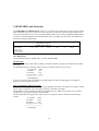
1
MAIN BOARD
User's Guide
(VER : 5V-1A)
User's Manual
The information presented in this publication has been carefully for reliability;
however no responsibility is assumed for inaccuracies.
Specifications are subject to change without notice.
TRADEMARKS
IBM
Intel/Pentium
Award
registered trademark of International Business Machines Corp.
registered trademark of Intel Corp.
registered trademark of Award Software Inc.
All other trademarks mentioned in this manual are registered
property of the respective owners.
COPYRIGHT
This manual may not in whole or in part, be photocopied,
reproduced transcribed translated or transmitted in whatsoever
from without the written consent of the manufacturer except for
Copies retained by the purchaser for personnel archival purposes.
2
Table of Contents
-----------------------------------------------------------------Chapter 1 Introduction............................................................... 4
1-1 Main Features............................................................................ 5
Chapter 2
2-1 Motherboard layout..................................................................6
2-2 Connectors.................................................................................7
2-3 Jumper setting............................................................................9
2-4 DRAM configuration.................................................................12
2-5 Cache memory configuration.....................................................12
Chapter 3 BIOS setup..................................................................13
3-1 Standard CMOS setup...............................................................14
3-2 BIOS Features setup..................................................................15
3-3 Chipset Features setup...............................................................18
3-4 Power Management setup..........................................................20
3-5 PNP/PCI Configuration............................................................. 22
3-6 Load BIOS defaults....................................................................23
3-7 Load Setup defaults....................................................................23
3-8 Integrated Peripherals........................................................ ........24
3-9 Password Setting................................................................. .......25
3-10 IDE HDD auto detection...........................................................26
3-11 Save & Exit Setup.....................................................................27
3-12 Exit without Saving...................................................................27
3
Chapter 1
Introduction
The VT82C580VPX mainboard combines the advanced capabilities of the VIA Apollo VPX
chipset with a high performance concurrent PCI local bus architecture to provide the ideal platform
for unleashing the unsurpassed speed and power of the Intel Pentium processor, Cyrix 6x86
and AMD K5/K6 processors, and can be easily upgraded for 321 pin ZIF socket.
The processor's advanced performance is complemented by a second level write back PB-SRAM up
to 512KB and main memory up to 512MB RAM. The main memory is initialed using the board's
two 72-pin SIMM sockets and two 168-pin DIMM sockets that accept either the new high
performance EDO, BEDO, or Fast Page mode DRAM.
The VT82C580VPX integrates a full set of I/O features on board, including two 16550 UART
compatible serial ports, one EPP/ECP capable port, one floppy disk controller, and one infrared
communication controller. On chip built in Enhanced IDE controller provides convenient, high
speed PCI bus Master connection capable of four IDE devices, including Hard disk and CD-ROM.
VIA builds all products to exact ing standards, using the highest quality components available.
We are proud to provide this system board and hope it brings you years of reliable service.
4
1-1 Main Features
* Supports
Intel Pentium (P54C) CPU speed 75/90/100/120/133/150/166/200/233MHZ
processors in a 321 pin ZIF socket, upgradable to P54C series/P54CT/P55C (optional
by splitting the voltage regulator). Cyrix6x86/6x86L/6X86MX/MII processors
AMD K5/K6/K6-2 processors.
*VIA Apollo VPX chipset includes a CPU interface controller, advanced cache controller,
intergrateed DRAM controller, asynchronous/ synchronous PCI local bus interface, intergraded
power management unit, internal keyboard controller, real-time clock.
* Support on board 256K/512K synchronous PBSRAM.
* Support synchronous DRAM using 168-pin DIMM modules of 8,16, 32.
(OPTIONAL).
* Take up to 256MB RAM in one bank using 72-pin SIMM modules of 1, 2, 4, 8, 16, 32,
64 or 128MB with supports for EDO,BEDO or Fast Page mode memory.
* Three 16-bit ISA expansion slots and three 32-bit PCI expansion slots.
* Integrated Enhanced PCI local bus IDE controller with two connectors support up to
four IDE devices such as Hard disk, CD-ROM.
* Integrated ITE IT8661F/RF multi I/O chipset that offers two 16550 UART compatible
serial ports, one EPP/ECP capable port, one IR port, and one Floppy Disk Drive
connector.
* Supports 128KB Flash ROM
* PCB size : 22 x 22.5 cm.
5
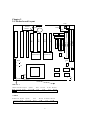
Chapter 2
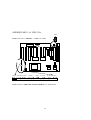
2-1 Motherboard Layout
JROM1
JBAT1
1
CN1
CN4
1
CN3
1
USB
AT
COM2
COM1
VT82C586A
VT82C585
DIMM1
DIMM2
SIMM2
SIMM1
IDE1
IDE2
FDC
PCI1
PCI2
PCI
PCI3
LPT1
JCK1
1
JCK4
CN11
JPW1
1
2
9
10
JD1
1
2
SOCKET 7
7
CN10
8
JV2
1
JBF0
JBF1
JBF2
1
3
VER. 2.2 A
TB-LED PW-LED Keylock
Speaker
Reset
SU-LED
SU-SW HD-LED
VER.2.2
POWER LED Keylock
Speaker
Reset
TB-LED
SUSPEND HD-LED
6
JV1
2
4
2-2 Connectors
CN3 - Keyboard connector
Pin
1
2
3
4
5
Description
Keyboard Clock
Keyboard Data
N.C.
Ground
+5 Vcc
CN4 - External PS/2 Mouse connector
CN5,CN6 - USB Connector (OPTIONAL)
CN7 - Power Supply Connector
Pin
1
2
3
4
5
6
Description
Power Good
+5V DC
+12V DC
-12V DC
Ground
Ground
Pin
7
8
9
10
11
12
7
Description
Ground
Ground
-5V DC
+5V DC
+5V DC
+5V DC
IDE1 - Primary IDE Connector
IDE2 - Secondary IDE Connector
CN9 - Floppy Disk Connector
COM1,2 - Serial Ports Connector
CN8 - Printer Port Connector
CN1 - Infrared Connector : IR
Pin
1
2
3
4
5
6
7
Signal Name
IRRX
Ground
IRTX
VCC
IRRXH
VCC
GND
8
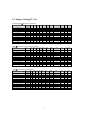
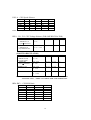
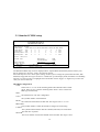
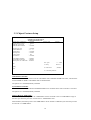
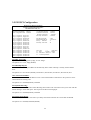
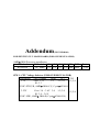
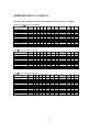
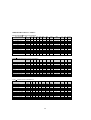
2-3 Jumper Setting(5V-1A)
Intel® Pentium Processor Installation
CPU CLOCK
P54C 75 MHZ
P54C 90 MHZ
P54C 100 MHZ
P54C 120 MHZ
P54C 133 MHZ
P54C 150 MHZ
P54C 166 MHZ
P55C 166 MHZ
P54C 180 MHZ
P54C 200 MHZ
P55C 200 MHZ
P55C 233 MHZ
3.3V
3.3V
3.3V
3.3V
3.3V
3.3V
3.3V
2.8V/3.3V
3.3V
3.3V
2.8V/3.3V
2.8V/3.3V
SYS.
JCK1 JCK2 JCK3 JCK4 JBF0
JBF1
JBF2
CLOCK
50 MHZ 2-3
2-3
2-3
1-2 OPEN OPEN OPEN
60 MHZ 1-2
2-3
2-3
2-3 OPEN OPEN OPEN
66 MHZ 2-3
1-2
2-3
2-3 OPEN OPEN OPEN
60 MHZ 1-2
2-3
2-3
2-3 CLOSE OPEN OPEN
66 MHZ 2-3
1-2
2-3
2-3 CLOSE OPEN OPEN
60 MHZ 1-2
2-3
2-3
2-3 CLOSE CLOSE OPEN
66 MHZ 2-3
1-2
2-3
2-3 CLOSE CLOSE OPEN
66 MHZ 2-3
1-2
2-3
2-3 CLOSE CLOSE OPEN
60 MHZ 1-2
2-3
2-3
2-3 OPEN CLOSE OPEN
66 MHZ 2-3
1-2
2-3
2-3 OPEN CLOSE OPEN
66 MHZ 2-3
1-2
2-3
2-3 OPEN CLOSE OPEN
66 MHZ 2-3
1-2
2-3
2-3 OPEN OPEN OPEN
JPW1
JV1
1-2,5-6,7-8
1-2,5-6,7-8
1-2,5-6,7-8
1-2,5-6,7-8
1-2,5-6,7-8
1-2,5-6,7-8
1-2,5-6,7-8
7-8
1-2,5-6,7-8
1-2,5-6,7-8
7-8
7-8
OPEN
OPEN
OPEN
OPEN
OPEN
OPEN
OPEN
1-2,3-4
OPEN
OPEN
1-2,3-4
1-2,3-4
JBF2
JPW1
JV1
OPEN
OPEN
OPEN
OPEN
OPEN
OPEN
OPEN
OPEN
CLOSE
CLOSE
CLOSE
CLOSE
1-2,3-4,5-6,7-8
1-2,3-4,5-6,7-8
1-2,3-4,5-6,7-8
1-2,3-4,5-6,7-8
1-2,7-8
1-2,7-8
5-6,7-8
1-2,5-6,7-8
3-4
3-4
3-4
3-4
OPEN
OPEN
OPEN
OPEN
1-2,3-4
1-2,3-4
1-2,3-4
1-2,3-4
1-2,3-4
1-2,3-4
1-2,3-4
1-2,3-4
JV2
1-2
1-2
1-2
1-2
1-2
1-2
1-2
1-2
1-2
1-2
1-2
1-2
RATIO
1.5X
1.5X
1.5X
2X
2X
2.5X
2.5X
2.5X
3X
3X
3X
3.5X
AMD K5/K6/K6-2 Processor Installation
CPU CLOCK
K5-PR 75
3.52V
K5-PR 90/PR120 3.52V
K5-PR100/PR133 3.52V
K5-PR166 3.52V
K6-PR166 2.9V/3.3V
K6-PR200 2.9V/3.3V
K6-PR233 3.2V/3.3V
K6-PR233 3.3V/3.3V
K6-PR266 2.2V/3.3V
K6-PR300 2.2V/3.45V
K6-2 266 2.2V/3.3V
K6-2 300 2.2V/3.3V
SYS.
JCK1 JCK2 JCK3 JCK4 JBF0
CLOCK
50 MHZ 2-3
2-3
2-3
1-2 OPEN
60 MHZ 1-2
2-3
2-3
2-3 OPEN
66 MHZ 2-3
1-2
2-3
2-3 OPEN
66 MHZ 2-3
1-2
2-3
2-3 CLOSE
66 MHZ 2-3
1-2
2-3
2-3 CLOSE
66 MHZ 2-3
1-2
2-3
2-3 OPEN
66 MHZ 2-3
1-2
2-3
2-3 OPEN
66 MHZ 2-3
1-2
2-3
2-3 OPEN
66 MHZ 2-3
1-2
2-3
2-3 CLOSE
66 MHZ 2-3
1-2
2-3
2-3 CLOSE
66 MHZ 2-3
1-2
2-3
2-3 CLOSE
66 MHZ 2-3
1-2
2-3
2-3 CLOSE
JBF1
OPEN
OPEN
OPEN
CLOSE
CLOSE
CLOSE
OPEN
OPEN
OPEN
CLOSE
OPEN
CLOSE
JV2 RATIO
1-2
1-2
1-2
1-2
1-2
1-2
1-2
1-2
1-2
2-3
1-2
1-2
1.5X
1.5X
1.5X
2.5X
2.5X
3X
3.5X
3.5X
4X
4.5X
4X
4.5X
Cyrix 6x86 Processor Installation
CPU CLOCK
P120+ M1 3.52V
P133+ M1 3.52V
P150+ M1 3.52V
P166+ M1 3.52V
P133+ 2.8V/3.3V 6X68L
P150 + 2.8V/3.3V 6X68L
P166+ 2.8V/3.3V 6X68L
P200+ 2.8V/3.3V 6X68L
MX PR 166 2.9V/3.3V
MX PR 200 2.9V/3.3V
MX PR 233 2.9V/3.3V
MII PR 300 2.9V/3.3V
SYS.
JCK1 JCK2 JCK3 JCK4 JBF0
JBF1
CLOCK
50 MHZ 2-3 2-3 2-3 1-2 CLOSE OPEN
55 MHZ 2-3 2-3 1-2 2-3 CLOSE OPEN
60 MHZ 1-2 2-3 2-3 2-3 CLOSE OPEN
66 MHZ 2-3 1-2 2-3 2-3 CLOSE OPEN
55 MHZ 2-3 2-3 1-2 2-3 CLOSE OPEN
60 MHZ 1-2 2-3 2-3 2-3 CLOSE OPEN
66 MHZ 2-3 1-2 2-3 2-3 CLOSE OPEN
75 MHZ 1-2 2-3 1-2 2-3 CLOSE OPEN
66 MHZ 2-3 1-2 2-3 2-3 CLOSE OPEN
75 MHZ 1-2 2-3 1-2 2-3 CLOSE OPEN
75 MHZ 1-2 2-3 1-2 2-3 CLOSE CLOSE
66 MHZ 2-3 1-2 2-3 2-3 OPEN OPEN
9
JBF2
JPW1
JV1
OPEN
OPEN
OPEN
OPEN
OPEN
OPEN
OPEN
OPEN
OPEN
OPEN
OPEN
OPEN
1-2,3-4,5-6,7-8
1-2,3-4,5-6,7-8
1-2,3-4,5-6,7-8
1-2,3-4,5-6,7-8
7-8
7-8
7-8
7-8
1-2,7-8
1-2,7-8
1-2,7-8
1-2,7-8
OPEN
OPEN
OPEN
OPEN
1-2,3-4
1-2,3-4
1-2,3-4
1-2,3-4
1-2,3-4
1-2,3-4
1-2,3-4
1-2,3-4
JV2
1-2
1-2
1-2
1-2
1-2
1-2
1-2
1-2
1-2
1-2
1-2
1-2
RATIO
2X
2X
2X
2X
2X
2X
2X
2X
2X
2X
2.5X
3.5X
JCK1-4 - CPU Speed Selector
Jumper 50MHZ 55MHZ 60MHZ 66MHZ
JCK1 2-3
2-3
1-2
2-3
JCK2 2-3
2-3
2-3
1-2
JCK3 2-3
1-2
2-3
2-3
JCK4 1-2/2-3 1-2/2-3 1-2/2-3 1-2/2-3
PCICLK 25/32 7.5/32
30/32
33.3/32
NOTE: JCK4 is synchronous/asynchronous selection.
75MHZ
1-2
2-3
1-2
1-2/2-3
37.5/32
JPW1 , JV1, JV2- CPU Voltage Selector (FOR ONE REGULATOR)
Description
1. P54C-STD,VR
2. AMD® K5-C,F
3. Cyrix 6X86-016
1. P54C-VRE
2. AMD® K5-B
3. Cyrix®6X86-028
CPU Voltage
Core: 3.3V
IO: 3.3
JPW1
1-2,5-6,7-8
JV1
OPEN
JV2
1-2
Core: 3.4 ~ 3.6V 1-2,3-4,5-6,7- OPEN
IO: 3.4 ~ 3.6V 8
1-2
(FOR TWO REGULATOR)
Description
1. INTEL® P55C
2. AMD® K5-H,J
3. Cyrix® 6x86L
1. AMD® K6
2. Cyrix 6x86MX
CPU Voltage
Core: 2.8V
IO: 3.3V
JPW1
7-8
JV1
1-2,3-4
JV2
1-2
Core: 2.9V
IO: 3.3V
1-2,7-8
1-2,3-4
1-2
AMD® K6 233
Core: 3.2V
IO: 3.3V
5-6,7-8
1-2,3-4
1-2
AMD® K6 300
Core: 2.2V
IO: 3.45V
1-2, 7-8 1-2, 3-4
2-3
NOTE : INTEL® P55C MMX, AMD® K6 AND CYRIX® 6X86L ARE “DUAL
VOLTAGE CPUs” , “6X86L” IS CYRIX® NEW LOW POWER CPU.
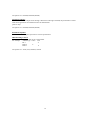
JBF0-JBF2 - CPU/BUS Ratio
Ratio
1.5X
2X
2.5X
3X
3.5X
4.0X
4.5X
JBF0
OPEN
CLOSE
CLOSE
OPEN
OPEN
CLOSE
CLOSE
JBF1
OPEN
OPEN
CLOSE
CLOSE
OPEN
OPEN
CLOSE
JBF2
OPEN
OPEN
OPEN
OPEN
OPEN
CLOSE
CLOSE
10
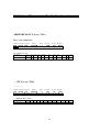
JBAT1 - CMOS Selector
Description
JBAT1
Normal (default)
1-2
Clear CMOS
2-3
(clear password)
JROM1 - Flash ROM Voltage Selector
Description
5V (SST,Winbond)
12V (Intel,MXIC)
JROM1
1-2
2-3
JD1 - DIMM Voltage Selector
Description
5V DIMM
3.3V DIMM
JD1
1-3,2-4
5-7,6-8
11
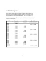
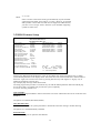
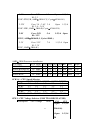
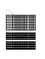
2-4 DRAM Configuration
System memory RAM is comprised of industry standard 72-pin Single In-line
Memory Modules (SIMMs). Burst Extended Data Out (BEDO) and Extended Data Out
(EDO) memory are the latest DRAM chip designs that perform a lot better than the Fast
Page mode DRAM type. With BEDO and EDO memory, CPU access to memory is 10
to 15% faster.
The VT82C580VP3 is able to support standard FPM (Fast Page Mode), EDO (Extended Data
Out), or BEDO (Burst Extended Data Out); memory can be installed in a variety of cong.,
as show in the following table:
Total Memory
8MB
8MB
12MB
16MB
16MB
16MB
24MB
32MB
32MB
32MB
40MB
48MB
64MB
64MB
64MB
72MB
80MB
96MB
128MB
128MB
Bank 0/1
(DIMM1)
8MB
Bank 2/3
(DIMM2)
Bank4/5
(SIMM1,SIMM2)
4MB & 4MB
8MB
8MB
16MB
4MB
8MB
8MB & 8MB
16MB
16MB
32MB
8MB
16MB
16MB & 16MB
32MB
32MB
32MB
64MB
8MB
16MB
32MB
32MB & 32MB
64MB
64MB
64MB
64MB
8MB
16MB
32MB
64MB
64MB & 64MB
.
12
2-5 Cache Memory Configuration
The VT82C580VP3 comes with onboard 256KB/512KB synchronous 3.3V Pipeline Burst SRAMs. Please
note that for 256K secondary cache, U20 and U15 should be mounted with 32x32 PBSRAM, otherwise
64x32 PBSRAM can offer 512K secondary cache.
Chapter 3 BIOS setup
Award's ROM BIOS provides a built-in Setup program which allows user to modify
the basic system configuration and hardware parameters. The modified data will be stored in a batterybacked CMOS ram so data will be retained even when the power is turned off
In general, the information saved in the CMOS ram stay unchanged unless there is config. change in the
system, such as hard drive replacement or new equipment change.
It is possible that CMOS had a battery failure which cause data loss in CMOS ram. If so,
re-enter system config. parameters become necessary.
TO ENTER SETUP PROGRAM
Power on the computer and press <Del> key immediately will bring you into BIOS CMOS SETUP
UTILITY.
ROM PCI/ISA BIOS (2A5LXXXX)
CMOS SETUP UTILITY
AWARD SOFTWARE, INC.
STANDARD CMOS SETUP
INTEGRATED PERIPHERALS
BIOS FEATURES SETUP
SUPERVISOR PASSWORD
CHIPSET FEATURES SETUP
USER PASSWORD
POWER MANAGEMENT SETUP
IDE HDD AUTO DETECTION
PNP/PCI CONFIGURATION
HDD LOW LEVEL FORMAT
LOAD SETUP DEFAULTS
SAVE & EXIT SETUP
EXIT WITHOUT SAVING
ESC : Quit
<--> : Select Item
F10 : Save & Exit Setup
(Shift)F2 : Change Color
The menu displays all the major selection items and allows user to select any one of show
item. The selection is made by moving cursor (press any direction key) to the item and press "enter" key. An
on line help message is displayed at the bottom of the screen as cursor is moving to various items which
provides user better understanding of each function. When a selection is made, the menu of selected item
will appear so the user can modify associated configuration parameters.
13
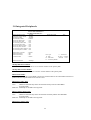
3-1 Standard CMOS setup
ROM PCI/ISA BIOS (2A5LXXX)
STANDARD CMOS SETUP
AWARD SOFTWARE, INC.
Date (mm:dd:yy) : Wed, Jan, 1 1997
Time (hh:mm:ss) : 00:00:00
HARD DISKS
TYPE SIZE CYLS HEAD PRECOMP LANDZ SECTOR MODE
Primary Master :
Auto
0
0
0
0
0
0
Auto
Primary Slave :
Auto
0
0
0
0
0
0
Auto
Secondary Master : Auto
0
0
0
0
0
0
Auto
Secondary Slave : Auto
0
0
0
0
0
0
Auto
Driver A : 1.44M, 3.5 in
Driver B : None
Video : EGA/VGA
Halt On : All Errors
ESC : Quit
F1 : Help
Base Memory
:
640K
Extended Memory :
7168K
Other Memory
:
384K
Total Memory
:
8192K
<--> : Select Item
PU/PD/+/- : Modify
(shift)F2 : Change Color
The Standard CMOS setup screen is displayed above, System BIOS automatically detects memory size,
thus no changes are necessary, it has a few items for setting.
Each item may have one or more option settings. It allows you to change the system Date and Time, IDE
hard disk, floppy disk drive types for drive A: and B: boot up video display mode, and POST error handling
selection. Use the arrow keys to highlights the item and then use the <Pgup> or <Pgdn> keys to select the
value you want in each item.
Hard Disk Configurations
TYPE :
Select from "1" to "45" to fill remaining fields with redefined values of disk
drives. Select "User" to fill the remaining fields. Select "Auto" to detect the
HDD type automatically.
SIZE :
The hard disk size. The unit is Mega Byte.
CYLS :
The cylinder number of the hard disk.
HEAD :
The read/write head number of hard disk. The range is from "1" to "16".
PRECOMP :
The cylinder number at which the disk drive changes the write timing.
LANDZ :
The cylinder number that the disk drive heads (read/write) are seated when
The disk drive is parked.
SECTOR :
The sector number of each track defined on the hard disk. The range is from
14
"1" to "64".
Mode :
Select "AUTO" to detect the mode type automatically. If your hard disk
supports the LBA mode, select "LBA" or "Large". However, if your hard
disk cyclinder is more than 1024 and does not support the LBA function,
you have to set at "Large". Select "Normal" if your hard disk supporting
cylinder is below 1024.
3-2 BIOS Features Setup
ROM PCI/ISA BIOS (2A5LXXXX)
BIOS FEATURES SETUP
AWARD SOFTWARE, INC.
Virus warning
: Disabled
Video BIOS Shadow
: Enabled
CPU Internal Cache
: Enabled
C8000-CBFFF Shadow : Disabled
External Cache
: Enabled
CC000-CFFFF Shadow : Disabled
Quick Power On Self Test : Disabled
D0000-D3FFF Shadow : Disabled
Boot Sequence
: A,C,SCSI
D4000-D7FFF Shadow : Disabled
Swap Floppy Drive
: Disabled
D8000-DBFFF Shadow : Disabled
Boot Up Floppy Seek
: Enabled
DC000-DFFFF Shadow : Disabled
Boot Up Numlock Status : On
Boot Up System Speed
: High
Gate A20 Option
: Normal
Typematic Rate Setting
: Disabled
Typematic Rate (Chars/Sec) : 6
Typematic Delay (Msec)
: 250
Security Option
: Setup
IDE Second Channel Control : Enabled
PCI/VGA Palette Snoop
: Disabled
ESC : Quit
<--> : Select Item
OS Select for DRAM>64MB : Non-OS2
F1 : Help
PU/PD/+/- : Modify
F5 : Old Values (Shift)F2 : Color
F7 : Load Setup Defaults
Selecting the "BIOS FEATURE SETUP" option in the CMOS setup utility menu allows user to change
system related parameters in the display menu. This menu shows all of the manufacturer's default values of
SV-P55V. Again, user can move the cursor by pressing direction keys and <PgDn> or <PgUp> key to
modify the parameters. Pressing [F1]
key to display help message of the selected item.
The setup program also provides 2 convenient ways to load the default parameter data from CMOS [F7]
area if shown data is corrupted. This provides the system a capability
to recover from any possible error.
Virus Warning:
When enabled, assigns the BIOS to monitor the master boot sector and the DOS boot sector of the first hard
disk drive.
The options are: Enabled, Disabled (Default)
CPU Internal Cache:
When enabled, improves the system performance. Disable this item when testing or trouble-shooting.
The options are : Enabled (Default), Disabled
External Cache:
When enabled, supports an optional cache SRAM.
15
The options are : Enabled (Default), Disabled
Quick Power On Self Test:
When enabled, allows the BIOS to bypass the extensive memory test.
The options are : Enabled, Disabled (Default)
Boot Sequence:
Allows the system BIOS to first try to boot the operating system from the selected disk drive.
The options are : A,C,SCSI (Default); C,A,SCSI; C,CDROM,A; CDROM,C,A; D,A,SCSI; E,A,SCSI;
F,A,SCSI; SCSI,A,C; SCSI,C,A; C only; LS/ZIP,C.
Swap Floppy Drive:
When enabled, allows you to switch the order in which the operating system accesses the floppy drives
during boot up.
The options are : Enabled, Disabled (Default)
Boot Up Floppy Seek:
When enabled, assigns the BIOS to perform floppy diskette drive tests by issuing the time-consuming seek
commands.
The options are : Enabled (Default), Disabled
Boot Up Numlock Status:
When set to On, allows the BIOS to automatically enable the Num Lock function when the system boots up.
The options are : On (Default), Off
Port 92H Fast A20G:
When enabled, allows the A20G bus line signal generated from the chipset 82C586 PC/AT to directly pass
to port 92H, instead of the keyboard controller. It will speed up the system performance.
The options are : Fast, Normal(Default)
Typematic Rate Setting:
The term "typematic" means that when a keyboard key is held down, the character is repeatedly entered
until the key is released. When this item is enabled, you may change the typematic repeat rate.
The options are : Disabled (Default), Enabled
Typematic Rate (Chars/Sec):
Sets the rate of a character repeat when the key is held down.
The options are : 6 (Default), 8, 10, 12, 15, 20, 24, 30
Typematic Delay (Msec):
Sets the delay time before a character is repeated.
The options are : 250 (Default), 500, 750, 1000 millisecond
16
Security Option:
Allows you to set the security level of the system.
The options are : Setup (Default), System
PCI/VGA Paiette Snoop:
When enabled, allows you install an enhanced graphics adapter card. If your graphics adapter card does not
support the Pallete Snoop function, please set at Disable to avoid system malfunctions.
The options are : Enabled, Disabled (Default)
Video BIOS Shadow:
When enabled, allows the BIOS to copy the video ROM code of the add-on video cards to the system
memory for faster access.
The options are : Enabled (Default), Disabled
C8000-CBFFF to DC000-DFFFF Shadow:
When enabled, allows the BIOS to copy the BIOS ROM code of the add-on card to system memory for
faster access. It may improve the performance of the add-on card.
Some add-on cards will not function properly if it’s BIOS ROM code is shadowed. To
use these options correctly, you need to know the memory address range used by the
BIOS ROM of each add-on card.
The options are : Enabled, Disabled (Default)
17
3-3 Chipset Features Setup
ROM PCI/ISA BIOS (2A5LXXXX)
CHIPSET FEATURES SETUP
AWARD SOFTWARE, INC.
DRAM Auto Configuration
: Disabled
On Chip USB
DRAM Timing Control
: Normal
SDRAM Cycle Length
: 3
SDRAM Bank Interleave
: Disabled
Sustained 3T write
2 Bank PBSRAM
Read Pipeline
Write Pipeline
Cache Timing
Linear Burst
:
:
:
:
:
:
: Disabled
Disabled
3-1-1-1
Disabled
Enabled
Fast
Disabled
Video BIOS Cacheable
: Disabled
System BIOS Cacheable
: Disabled
Memory Hole At 15MB Addr. : Disabled
ESC : Quit
<--> : Select
F1 : Help
PU/PD/+/- :
item
Modify
F5 : Old Values
(Shift)F2 :
Color
F7 : Load Setup Defaults
Video BIOS Cacheable:
When enabled, allows the system to use the video BIOS codes C0000H-C7FFFH from cache, instead of the
slower DRAMs or ROMs. Video BIOS must be shadowed first.
The options are : Enabled (Default), Disabled
System BIOS Cacheable:
When enabled, allows the ROM area E0000H-FFFFFH to be cacheable when cache controller is activated.
The options are : Enabled (Default), Disabled
Memory Hold At 15MB Addr.:
When enabled, the memory hole at the 15MB address will be relocated to the 15~16MB address range of
the ISA cycle when the processor accesses the 15~16MB address area.
When disabled, the memory hole at the 15MB address will be treated as a DRAM cycle when the processor
accesses the 15~16MB address.
18
The options are : Enabled, Disabled (Default)
Sustained 3T Write:
The cache architecture adopts Write Through. When Write Through is enabled, the performance is better
under most application environment because the 580VP FIFO
queue is deep.
The options are : Enabled, Disabled (Default)
Read/Write Pipeline:
Turn on Read/Write Pipeline operation to increase performance.
DRAM Timing Control:
Allows you to speed up the data access of 82C585M.
For example:
DRAM type Turbo
Fast
FP-7
V
EDO-6
V
EDO-7
V
The options are : Turbo, Fast, Medium, Normal
19
3-4 Power Management Setup
**PM Timer**
HDD Power Down
Doze Mode
Suspend Mode
ROM PCI/ISA BIOS (2A5LXXXX)
POWER MANAGEMENT SETUP
AWARD SOFTWARE, INC.
: User Defined
IRQ5 (LPT2)
: Primary
: Yes
IRQ6 (Floppy Disk)
: Primary
: Suspend->Off
IRQ7 (LPT1)
: Primary
: V/H SYNC+ Blank
IRQ8 (RTC Alarm)
: Disabled
: Disabled
IRQ9 (IRQ2 Redir) : Secondary
:3
IRQ10 (Reserved)
: Secondary
IRQ11 (Reserved)
: Secondary
IRQ12 (PS/2 Mouse) : Primary
: Disable
IRQ13 (Coprocessor) : Primary
: Disbale
IRQ14 (Hard Disk)
: Primary
: Disable
IRQ15 (Reserved)
: Disabled
**PM Events**
VGA
LPT & COM
HDD & FDD
DMA/MASTER
Primary INTR
IRQ3 (COM2)
IRQ4 (COM1)
: OFF
: LPT/COM
: ON
: OFF
: ON
: Primary
: Primary
Power Management
PM Control by APM
Video off Option
Video off Method
Conserve Mode
Moden Use IRQ
ESC : Quit
<--> : Select Item
F1 : Help
PU/PD/+/- : Modify
F5 : Old Values
(Shift) F2 : Color
F7 : Load Setup Defaults
Power Management:
When enable, allows you to use Power Management features.
PM Control by APM:
The option "No" allows the BIOS to ignore the APM (Advanced Power Management)
specification. Selecting "Yes" will allow the BIOS wait for APM's prompt before it
enters Doze mode, Standby mode, or Suspend mode. If the APM is installed, it will
prompt the BIOS to set the system into the power saving mode after all tasks are done.
Video off Option:
This feature provides the selections of the video display power saving mode. The option
"Suspend -> Off" allows the display blanks if the system enters Suspend mode. The option "All modes ->
Off" allows the video display banks if the system enters Doze mode or Suspend mode. The option "Always
On" allows the video display to stay in Standby mode even the system enters Doze or Suspend mode.
Video Off Method:
The option "V/H SYNC+ Blank" allows the BIOS to blank off screen display by turning off the V-Sync
signals sent from add-on VGA card. "DPMS Supported" allows the BIOS to blank off screen display by
your add-on VGA card which supports DPMS
(Display Power Management Signaling function). "Blank Screen" allows the BIOS to blank screen display
by turning off the red-green-blue signals.
20
Conserve Mode:
When the Doze Mode of the system being happened, the Doze Mode is handled by hardware not by SMI
function.
Modem use IRQ:
When the system is in green function, modem wakes up the system through IRQ.
HDD Power Down:
Selecting "Disabled" will turn off the hard disk drive (HDD) motor.
Selecting "1Min ...15Min" allows you to define the HDD idle time before the HDD enters Power Saving
mode.
The option "When Suspend" lets the BIOS turn the HDD motor off when the system is in Suspend mode.
The options "1Min ... 15Min" and "When Suspend" will not work concurrently. When HDD is in Power
Saving Mode, any access to the HDD will wake the HDD up.
Doze Mode:
When disabled, the system will not enter Doze mode. The specified time option define the idle time the
system takes before it enters Doze mode.
Suspend Mode:
When disabled, the system will not enter Suspend mode. The specified time option defines the idle time the
system takes before it enters Suspend mode.
VGA:
Selecting "ON" will enable the power management timers when a "no activity" events is
detected in the VGA. Selecting "OFF" to disable the PM timer even if a "no activity" event is detected.
LPT & COM:
Selecting "LPT & COM" will enable the power management timers when a "no activity"
event is detected in the LPT and COM ports. Selecting "LPT" ("COM") will enable the power management
timers when a "no activity" event is detected in the LPT (COM) ports.
Selecting "NONE" to disable the PM timer even if a "no activity" event is detected.
HDD & FDD:
Selecting "ON" will enable the power management timers when a "no activity" event is detected in the hard
disk drive and floppy disk drive. Selecting "OFF" to disable the PM timer event if a "no activity" event is
detected.
DMA/Master:
When the master is working, the system will not have SMI signal until the master is finished.
Primary INTR:
When enabled, you can choose any IRQ#.
IRQ#:
When set at "Primary" the processor will power down only after the BIOS detects a "no IRQ activity"
during the time specified by the Suspend time. If set at "Secondary event"
the system will distinguish whether an interrupt accesses an I/O address or not. If it does, the system enters
the standby mode. If not, the system enters the dreaming mode; that is the system goes back full-on status
but leaves the monitor blank. For instance, if the system connects to a LAN and receives an interrupt from
its file server, the system will enter the dreaming mode to execute the corresponding calling routine.
21
3-5 PNP/PCI Configuration
ROM PCI/ISA BIOS (2A5LXXXX)
PNP/PCI CONFIGURATION SETUP
AWARD SOFTWARE, INC.
PNP OS Installed
: No
CPU to PCI Write Buffer : Enabled
Resources Controlled By : Manual
PCI Dynamic Bursting
: Enabled
Reset Configuration Data : Disabled
PCI Master 0 WS Write
: Enabled
PCI Peer Concurrency
: Disabled
IRQ-3 assigned to : Legacy ISA
PCI Delay Transaction
: Disabled
IRQ-4 assigned to : Legacy ISA
IRQ-5 assigned to : PCI/ISA PnP
PCI IRQ Actived By
: Edge
IRQ-7 assigned to : Legacy ISA
PCI IDE IRQ Map To
: PCI-AUTO
IRQ-9 assigned to : PCI/ISA PnP
Primary
IDE INT#
:A
IRQ-10 assigned to : PCI/ISA PnP
Secondary IDE INT#
:B
IRQ-11 assigned to : PCI/ISA PnP
IRQ-12 assigned to : PCI/ISA PnP
IRQ-14 assigned to : Legacy ISA
IRQ-15 assigned to : Legacy ISA
DMA-0 assigned to : PCI/ISA PnP
DMA-1 assigned to : PCI/ISA PnP
ESC : Quit
<-->
: Select Item
DMA-3 assigned to : PCI/ISA PnP
F1 : Help
PU/PD/+/- : Modify
DMA-5 assigned to : PCI/ISA PnP
F5 : Old Valucs (Shift) F2 : Color
DMA-6 assigned to : PCI/ISA PnP
F7 : Load Setup Defaults
DMA-7 assigned to : PCI/ISA PnP
PCI IRQ Actived By:
If your IDE cards is triggered by edge, set it at "Edge".
The options are : Level, Edge (Default)
PCI IDE IRQ Map To:
Set to auto to allow the system BIOS to automatically detect which interrupt is used by the PCI master
drive.
The options are : PCI-AUTO (Default), PCI-SLOT1, PCI-SLOT2, PCI-SLOT3, PCI-SLOT4, ISA
CPU to PCI Write Buffer:
When enabled, allows data and address access to the internal buffer of 82C586A so the processor can be
released from the waiting state.
The options are : Enabled (Default), Disabled
PCI Dynamic Bursting:
When enabled, the PCI controller allows Bursting PCI transfer if the consecutive PCI cycles come with the
address falling in same 1KB space. This improves the PCI bus through put.
The options are : Enabled (Default), Disabled.
PCI Master 0 WS Write:
When enabled, allows a zero-wait-state-cycle delay when the PCI master drive writes data to DRAM.
The options are : Enabled, Disabled (Default)
22
3-6 Load BIOS Defaults
The BIOS defaults contain the most appropriate values of the system parameters that allows minimum
system performance. The OEM manufacturer may change the defaults through MODBIN before the binary
image burns into the ROM.
3-7 Load Setup Defaults
Selecting this field loads the factory defaults for BIOS and Chipset Features which the system automatically
detects.
23
3-8 Integrated Peripherals
ROM PCI/ISA BIOS (2A5LXXXX)
INTEGATED PERIPHEALS
AWARD SOFTWARE, INC.
OnChip IDE first channel
: Enabled
Onchip IDE second channel
: Enabled
IDE Prefetch Mode
: Enabled
IDE HDD Block Mode
: Enabled
IDE Primary Master PIO
: Auto
IDE Primary Slave PIO
: Auto
IDE Secondary Master PIO
: Auto
IDE Secondary Slave PIO
: Auto
IDE Primary Master UDMA : Auto
IDE Primary Slave UDMA
: Auto
IDE Secondary Master UDMA: Auto
IDE Secondary Slave UDMA : Auto
Onboard FDC Controller
Onboard Serial Port 1
Onboard Serial Port 2
IR Address Select
: Enabled
: Auto
: Auto
: Disable
Onboard Parallel Port
: 378/IRQ7
Parellel Port Mode
: SPP
ESC : Quit
<--> : Select Item
F1 : Help
PU/PD/+/- : Modify
F5 : Old Values
(Shift)F2 : Color
F7 : Load Setup Default
OnChip IDE First Channel:
When enabled, allows the IDE driver to use the first channel of the primary IDE.
OnChip IDE Second Channel:
When enabled, allows the IDE drive to use the second channel of the primary IDE.
IDE Prefetch Mode:
When enabled, allows the system BIOS to utilize the prefetch buffer of the onboard IDE controller to
prefetch the next sequential data of the current access.
IDE Primary Slave PIO:
The default value is Auto.
Auto:
BIOS will automatically detect the Onboard Primary Slave PCI IDE HDD
accessing mode.
Mode 0-4 : Manually set the IDE accessing mode.
IDE Secondary Master PIO:
The default value is Auto.
Auto
: BIOS will automatically detect the Onboard Secondary Master PCI IDE HDD
accessing mode.
Mode 0-4 : Manually set the IDE accessing mode.
IDE Primary Master PIO:
The default value is Auto.
24
IDE Secondary Slave PIO:
The default value is Auto.
Onboard FDC Controller:
The default value is Enabled.
Enabled : Enabled the onboard I/O Chip's floppy drive interface controller.
Disabled : Disabled the onboard I/O Chip's floppy drive interface controller. When use on-card ISA FDC's
controller.
Onboard Serial Port 1:
The field allows the user to select the serial port. The default value is AUTO.
COM1: Enable onboard serial port1 and address is COM1/3F8H
COM2: Enable onboard serial port1 and address is COM2/2F8H
COM3: Enable onboard serial port1 and address is COM3/3E8H
COM4: Enable onboard serial port1 and address is COM4/2E8H
Disabled: Disable onboard I/O Chip's Serial port 1.
AUTO : BIOS will automatically detect the Onboard Serial Port.
Onboard Serial Port 2:
The field allows the user to select the serial port. The default value is AUTO.
COM1: Enable onboard serial port1 and address is COM1/3F8H
COM2: Enable onboard serial port1 and address is COM2/2F8H
COM3: Enable onboard serial port1 and address is COM3/3E8H
COM4: Enable onboard serial port1 and address is COM4/2E8H
Disabled: Disable onboard I/O Chip's Serial port 1.
AUTO : BIOS will automatically detect the Onboard Serial Port.
Onboard Parallel Port:
The field allows the user to select the LPT port. The default value is 378H/IRQ7.
378H : Enable onboard LPT port and address is 378H and IRQ7
278H : Enable onboard LPT port and address is 278H and IRQ5
3BCH : Enable onboard LPT port and address is 3BCH and IRQ7
Disabled : Disable onboard I/O Chip's LPT port
3-9 Password Setting
1.If CMOS is corrupted or the option was not used, a default password stored in the ROM will be used. The
screen will display the following message:
Enter Password
Press the [Enter] key to continue after proper password is given
2.If CMOS is corrupted or the option was used earlier and the user wish to change default password, the
SETUP UTILITY will display a message and ask for a confirmation.
Confirm Password:
3.After pressing the [Enter] key (ROM password if the option was not used) or current password (userdefined password), the user can change the password and store new one in CMOS RAM. A maximum of 8
characters can be entered.
25
3-10 IDE HDD Auto Detection
The "IDE HDD AUTO DETECTION" utility is a very useful tool specially when you do not know which
kind of hard disk type you are using. You can use this utility to detect the correct disk type installed in the
system automatically. But now you can set HARD DISK TYPE to auto in the STANDARD CMOS SETUP.
You don't need the"IDE HDD AUTO DETECTION" utility. The BIOS will Auto-detect the hard disk size
and model on display during POST.
HARD DISK
Primary Master
Primary Slave
Secondary Master
Secondary Slave
TYPE
ROM PCI/ISA BIOS (2A5LXXXX)
CMOS SETUP UTILITY
AWARD SOFTWARE, INC.
SIZE CYLS HEADS PRECOMP LANDZONE
343
665
16
65535
664
SECTORS
63
MODE
Normal
Note: HDD modes
The Award BIOS supports 3 HDD modes : Normal, LBA&LARGE.
Normal mode:
Generic access mode in which either the BIOS or the IDE controller will make any transformations during
accessing.
The maximum number of cylinders, head & sectors for Normal mode are 1024, 16 & 63.
no.Cyclinder (1024)
x no.Head
(16)
x no.Sector
(63)
x no.per sector
(512)
------------------------------528 Megabytes
If user set in Normal mode, the maximum accessible HDD size will be 528 Megabyte even though its
physical size may be greater than that !
LBA (Logical Block Addressing) mode:
A new HDD accessing method to overcome the 528 Megabyte bottleneck. The number of cylinders, head &
sectors show in setup may not be the number physically contained in the HDD.
During HDD accessing, the IDE controller will transform the logic address described by sector, head &
cylinder into its own physical address inside the HDD.
The maximum HDD size supported by LBA mode is 8.4 Gigabytes which is obtained by the following
formula:
no.Cylinder
(1024)
x no.Head
(255)
x no.Sector
(63)
x bytes.per sector (512)
-------------------------------8.4 Gigabytes
26
LARGE mode:
Extended HDD access mode supported by Award Software.
Some IDE HDDs contain more than 1024 cylinder without LBA support(in some cases, user do not want
LBA). The Award BIOS provides another alternative to support these kinds of LARGE mode:
CYLS.
1120
560
HEADS
16
32
SECTOR
59
59
MODE
Normal
Large
BIOS tricks DOS (or other OS) that the number of cylinders is less than 1024 by dividing it by 2. At the
same time, the number of heads is multiplied by 2. Averse transformation process will be made inside INT
12h in order to access the right HDD addess the right HDD address !
no.Cylinder
(1024)
x no.Head
(32)
x no.Sector
(63)
x bytes.per sector (512)
-----------------------------1 Gigabytes
Note:
To support LBA or LARGE mode of HDDs, there must be some softwares involved. All these
softwares are located in the Award HDD Service Routine (INT 13h). It may be failed to access
a HDD with LBA (LARGE) mode selected if you are runing under a operating system which
replaces the whole INT 13h. UNIX operating systems do not support either or LARGE and
must utilize the standard mode. UNIX can support drives large than 528MB.
3-11 Save & Exit Setup
After you have made changes under Setup, press <ESC> to return to the main menu. Move cursor to "Save
and Exit Setup" or press "F10" and then press "Y" to change the CMOS setup. If you did not change
anything, press <ESC> again or move cursor to "Exit Without Saving" and press "Y" to retain the Setup
settings.
The following message will appear at the center of the screen to allow you to save data to CMOS and exit
the setup utility.
SAVE to CMOS and EXIT (Y/N)?
3-12 Exit Without Saving
The "EXIT WITHOUT SAVING" option will bring you back to normal boot up procedure without saving
any into CMOS RAM.
All of the old data in the CMOS will not be destroyed.
If you select this feature, the following message will appear at the center of the screen to allow you to exit
the setup utility without saving CMOS modifications:
Quit Without Saving(Y/N)?
5V-1A-2
END
27
Addendum
(TEXT ERROR)
FOR PENTIUN 5V-2 MAIN BOARD (FOR ONE REGULATOR)
AMD 5K86 Processor installation
CPU clock
SYS. clock JCK1 JCK2JCK3JCK4JBF1 JBF2
K5-PR166
66 MHZ 2-3 1-2 2-3 1-2 close close
JPW1 - CPU Voltage Selector (FOR ONE REGULATOR)
Description CPU Voltage
JPW1
JV1
JV2
JV2
3.3V
Core: 3.3V
1-2
1-2,3-4 1-3,2-4
1-3,2-4
IO: 3.3
(P54C-STD,VR, AMD 5K86-C,F, Cyrix 6X86-016)
3.52V
Core: 3.4 ~ 3.6V 3-4 1-2,3-4
IO: 3.4 ~ 3.6V
(P54C-VRE, AMD 5K86-B, Cyrix 6X86-028)
28
1-3,2-4
Ratio
2.5x
FOR OLD VER JUMPER SETTING
Description
3.3V
CPU Voltage
JPW1
JV1
JV2
Core: 3.3V
1-2
1-2,3-4 1-2,3-4
IO: 3.3
(P54C-STD,VR, AMD 5K86-C,F, Cyrix 6X86-016)
3.52V
Core: 3.4 ~ 3.6V 3-4 1-2,3-4 Open
IO: 3.4 ~ 3.6V
(P54C-VRE, AMD 5K86-B, Cyrix 6X86-028)
2.8V
Core: 2.7 ~ 2.9V 5-6
IO: 3.3V
(P55C, AMD 5K86-H,J)
2.5V
Core: 2.5V
IO: 3.3V
(P55C, AMD 5K86-K)
7-8
29
1-2,3-4 Open
1-2,3-4 Open
Addendum
(TEXT ERROR)
FOR PENTIUN 5V-2 MAIN BOARD (FOR TWO REGULATOR)
AMD 5K86 Processor installation
CPU clock
SYS. clock JCK1 JCK2JCK3JCK4JBF1 JBF2
K86-PR166
66 MHZ 2-3 1-2 2-3 1-2 close close
JCK1-4 - CPU Speed Selector
Jumper 50MHZ 55MHZ 60MHZ 66MHZ 75MHZ
JCK1
2-3
2-3
1-2
2-3
1-2
JCK2
2-3
2-3
2-3
1-2
2-3
JCK3
2-3
1-2
2-3
2-3
1-2
JCK4
1-2
1-2
1-2
1-2
1-2
PCICLK 25/32 27.5/32 30/32 33.3/32 37.5/32
JPW1 - CPU Voltage Selector (FOR TWO REGULATOR)
Description CPU Voltage
JPW1
JV1
JV2
JV2
Open 1-3,2-4
X86-016)
Open
1-3,2-4
28
1-2,3-4 Open
1-2,3-4 Open
30
Ratio
2.5x
3.3V
Core: 3.3V
1-2
Open 1-3,2-4
IO: 3.3
(P54C-STD,VR, AMD 5K86-C,F, Cyrix 6X86-016)
3.52V
Core: 3.4 ~ 3.6V 3-4
Open 1-3,2-4
IO: 3.4 ~ 3.6V
(P54C-VRE, AMD 5K86-B, Cyrix 6X86-028)
2.8V
Core: 2.8V
5-6
1-2,3-4 Open
IO: 3.3V
(P55C, AMD 5K86-H,J, Cyrix 6X86L)
2.5V
Core: 2.5V
IO: 3.3V
(P55C, AMD 5K86-K)
7-8
1-2,3-4 Open
AMD 5K86 Processor installation
CPU clock
SYS. clock JCK1 JCK2JCK3JCK4JBF1
K86-PR75
50 MHZ 2-3 2-3 2-3 1-2 open
K86-PR90/PR120
60 MHZ 1-2 2-3 2-3 1-2 open
K86-PR100/PR133 66 MHZ 2-3 1-2 2-3 1-2 open
K86-PR166
66 MHZ 2-3 1-2 2-3 1-2 close
JBF2
open
open
open
close
JCK1-4 - CPU Speed Selector
Jumper 50MHZ 55MHZ 60MHZ 66MHZ 75MHZ
JCK1
2-3
2-3
1-2
2-3
1-2
JCK2
2-3
2-3
2-3
1-2
2-3
JCK3
2-3
1-2
2-3
2-3
1-2
JCK4
1-2
1-2
1-2
1-2
1-2
PCICLK 25/32 27.5/32 30/32 33.3/32 37.5/32
JPW1 - CPU Voltage Selector (FOR TWO REGULATOR)
Description CPU Voltage
JPW1
JV1
JV2
JV2
Open 1-3,2-4
31
X86-016)
Open
28
1-3,2-4
Ratio
1.5x
1.5x
1.5x
2.5x
3.3V
Core: 3.3V
1-2
Open 1-3,2-4
IO: 3.3
(P54C-STD,VR, AMD 5K86-C,F, Cyrix 6X86-016)
3.52V
Core: 3.4 ~ 3.6V 3-4
Open 1-3,2-4
IO: 3.4 ~ 3.6V
(P54C-VRE, 1 5K86-B, Cyrix 6X86-028)
2.8V
Core: 2.8V
IO: 3.3V
(P55C, AMD 5K86-H,J)
5-6
1-2,3-4 Open
2.5V
7-8
1-2,3-4 Open
Core: 2.5V
IO: 3.3V
(P55C, AMD 5K86-K)
Addendum
FOR PENTIUN 5V-2 MAIN BOARD (FOR TWO REGULATOR)
PLEASE UPDATE MANUAL WITH FOLLOWING AMENDMENTS :
1. PAGE 6 : CHAPTER 2 2-1 MOTHERBOARD LAYOUT
JV2 SHOULD BE POSITIONED
1
3
2
4
2. PAGE 10 : AMD 5K86 PROCESSOR INSTALLATION
AMD 5K86 Processor installation
CPU clock
SYS. clock JCK1 JCK2JCK3JCK4JBF1 JBF2
*K86-PR150
60 MHZ 1-2 2-3 2-3 1-2 close close
*K86-PR166
66 MHZ 2-3 1-2 2-3 1-2 close close
NOTE: " * " -- This CPU had not been tested when this manual was printed.
3. PAGE 10 : JPW1 - CPU VOLTAGE SELECTOR
32
Ratio
2.5x
2.5x
JPW1 - CPU Voltage Selector (FOR TWO REGULATOR)
Description CPU Voltage
JPW1
JV1
JV2
3.3V
Core: 3.3V
1-2
Open 1-2,3-4
IO: 3.3
(P54C-STD,VR, AMD K5-C,F, Cyrix 6X86-016)
3.52V
Core: 3.4 ~ 3.6V 3-4
Open 1-2,3-4
IO: 3.4 ~ 3.6V
(P54C-VRE, AMD K5-B, Cyrix 6X86-028)
2.8V
Core: 2.8V
5-6
1-2,3-4 Open
IO: 3.3V
(INTEL P55C, AMD K5-H,J, Cyrix 6x86L)
2.5V
Core: 2.5V
IO: 3.3V
(INTEL P55C, AMD K5-K)
7-8
1-2,3-4 Open
Addendum
FOR PENTIUN 5V-2 MAIN BOARD (FOR ONE REGULATOR)
PLEASE UPDATE MANUAL WITH FOLLWING AMENDMENTS :
1. PAGE 6 : CHAPTER 2 2-1 MOTHERBOARD LAYOUT
JV2 SHOULD BE POSITIONED
1
3
2
4
2. PAGE 10 : AMD 5K86 PROCESSOR INSTALLATION AMD 5K86
Processor installation
CPU clock
SYS. clock JCK1 JCK2JCK3JCK4JBF1 JBF2 Ratio
*K86-PR150
60 MHZ 1-2 2-3 2-3 1-2 close close 2.5x
*K86-PR166
66 MHZ 2-3 1-2 2-3 1-2 close close 2.5x
NOTE: " * " -- This CPU had not been tested when this manual was peinted.
3. PAGE 10 : JPW1 - CPU VOLTAGE SELECTOR
JPW1 - CPU Voltage Selector (FOR ONE REGULATOR)
33
Description
3.3V
CPU Voltage
JPW1
JV1
JV2
JV2
Core: 3.3V
1-2
1-2,3-4 1-3,2-4
1-2,3-4
IO: 3.3
(P54C-STD,VR, AMD 5K86-C,F, Cyrix 6X86-016)
3.52V
Core: 3.4 ~ 3.6V 3-4 1-2,3-4
IO: 3.4 ~ 3.6V
(P54C-VRE, AMD 5K86-B, Cyrix 6X86-028)
1-3,2-4
1-2,3-4
Addendum
FOR PENTIUN 5V-2 MAIN BOARD (FOR TWO REGULATOR)
PLEASE UPDATE MANUAL WITH FOLLWING AMENDMENTS :
1. PAGE 6 : CHAPTER 2 2-1 MOTHERBOARD LAYOUT
JV2 SHOULD BE POSITIONED
1
3
2
4
2. PAGE 10 : AMD 5K86 PROCESSOR INSTALLATION
Cyrix 6x86 Processor installation
CPU clock SYS. clock JCK1 JCK2 JCK3 JCK4 JBF1 JBF2 Ratio
6X68L 133 55 MHZ 2-3 2-3 1-2 1-2 close open 2x
6X86L 150 60 MHZ 1-2 2-3 2-3 1-2 close open 2x
6X86L 166 66 MHZ 2-3 1-2 2-3 1-2 close open 2x
6X86L 200 75 MHZ 1-2 2-3 1-2 1-2 close open 2x
NOTE: " * " -- This CPU had not been tested when this manual was peinted.
3. PAGE 10 : JPW1 - CPU VOLTAGE SELECTOR
JPW1 - CPU Voltage Selector (FOR TWO REGULATOR)
JV1
JV2
Description
CPU Voltage
JPW1
JV1
Open 1-2,3-4
6-016)
Open
1-2,3-4
)
1-2,3-4
34 Open
6L)
1-2,3-4
Open
3.3V
Core: 3.3V
1-2
Open
IO: 3.3
(P54C-STD,VR, AMD K5-C,F, Cyrix 6X86-016)
1-3,2-4
3.52V
1-3,2-4
Core: 3.4 ~ 3.6V 3-4
Open
IO: 3.4 ~ 3.6V
(P54C-VRE, AMD K5-B, Cyrix 6X86-028)
2.8V
Core: 2.8V
5-6
1-2,3-4 Open
IO: 3.3V
(INTEL P55C, AMD K5-H,J, Cyrix 6x86l)
2.5V
Core: 2.5V
IO: 3.3V
(INTEL P55C, AMD K5-K)
7-8
1-2,3-4 Open
Addendum
FOR PENTIUN 5V-2 MAIN BOARD (FOR TWO REGULATOR)
PLEASE UPDATE MANUAL WITH FOLLWING AMENDMENTS :
AMD K5/K6 Processor installation
CPU clock
SYS. clock JCK1 JCK2JCK3JCK4JBF1
K6-PR166
66 MHZ 2-3 1-2 2-3 1-2 close
K6-PR200
66 MHZ 2-3 1-2 2-3 1-2 open
K6-PR233
66 MHZ 2-3 1-2 2-3 1-2 open
3. PAGE 10 : JPW1 - CPU VOLTAGE SELECTOR
JPW1 - CPU Voltage Selector (FOR TWO REGULATOR)
JV1
JV2
Description
CPU Voltage
JPW1
JV1
Open 1-2,3-4
6-016)
Open
1-2,3-4
)
1-2,3-4
35 Open
6L)
1-2,3-4
Open
JBF2
close
close
open
Ratio
2.5x
3x
3.5x
3.3V
Core: 3.3V
1-2
Open
IO: 3.3
(P54C-STD,VR, AMD K5-C,F, Cyrix 6X86-016)
1-3,2-4
3.52V
1-3,2-4
Core: 3.4 ~ 3.6V 3-4
Open
IO: 3.4 ~ 3.6V
(P54C-VRE, AMD K5-B, Cyrix 6X86-028)
2.8V
Core: 2.8V
5-6
1-2,3-4 Open
IO: 3.3V
(INTEL P55C, AMD K5-H,J, Cyrix 6x86l)
2.5V
Core: 2.5V
IO: 3.3V
(INTEL P55C, AMD K5-K)
7-8
1-2,3-4 Open
36
ADDENDUM(5V-1A VER.2.2)
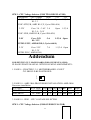
PLEASE FIND THE BELOW UPDATE JUMPER SETTINGS FOR 5V-1A, VER2.2:
Intel® Pentium Processor Installation
CPU CLOCK
P54C 75 MHZ
P54C 90 MHZ
P54C 100 MHZ
P54C 120 MHZ
P54C 133 MHZ
P54C 150 MHZ
P54C 166 MHZ
P55C 166 MHZ
P54C 180 MHZ
P54C 200 MHZ
P55C 200 MHZ
P55C 233 MHZ
3.3V
3.3V
3.3V
3.3V
3.3V
3.3V
3.3V
2.8V/3.3V
3.3V
3.3V
2.8V/3.3V
2.8V/3.3V
SYS.
JCK1 JCK2 JCK3 JCK4 JBF0
JBF1
JBF2
CLOCK
50 MHZ 2-3
2-3
2-3
1-2 OPEN OPEN OPEN
60 MHZ 1-2
2-3
2-3
2-3 OPEN OPEN OPEN
66 MHZ 2-3
1-2
2-3
2-3 OPEN OPEN OPEN
60 MHZ 1-2
2-3
2-3
2-3 CLOSE OPEN OPEN
66 MHZ 2-3
1-2
2-3
2-3 CLOSE OPEN OPEN
60 MHZ 1-2
2-3
2-3
2-3 CLOSE CLOSE OPEN
66 MHZ 2-3
1-2
2-3
2-3 CLOSE CLOSE OPEN
66 MHZ 2-3
1-2
2-3
2-3 CLOSE CLOSE OPEN
60 MHZ 1-2
2-3
2-3
2-3 OPEN CLOSE OPEN
66 MHZ 2-3
1-2
2-3
2-3 OPEN CLOSE OPEN
66 MHZ 2-3
1-2
2-3
2-3 OPEN CLOSE OPEN
66 MHZ 2-3
1-2
2-3
2-3 OPEN OPEN OPEN
JPW1
JV1
1-2,5-6,7-8
1-2,5-6,7-8
1-2,5-6,7-8
1-2,5-6,7-8
1-2,5-6,7-8
1-2,5-6,7-8
1-2,5-6,7-8
7-8
1-2,5-6,7-8
1-2,5-6,7-8
7-8
7-8
OPEN
OPEN
OPEN
OPEN
OPEN
OPEN
OPEN
1-2,3-4
OPEN
OPEN
1-2,3-4
1-2,3-4
JBF2
JPW1
JV1
OPEN
OPEN
OPEN
OPEN
OPEN
OPEN
OPEN
OPEN
CLOSE
CLOSE
1-2,3-4,5-6,7-8
1-2,3-4,5-6,7-8
1-2,3-4,5-6,7-8
1-2,3-4,5-6,7-8
1-2,7-8
1-2,7-8
5-6,7-8
1-2,5-6,7-8
3-4
3-4
OPEN
OPEN
OPEN
OPEN
1-2,3-4
1-2,3-4
1-2,3-4
1-2,3-4
1-2,3-4
1-2,3-4
JV2
1-2
1-2
1-2
1-2
1-2
1-2
1-2
1-2
1-2
1-2
1-2
1-2
RATIO
1.5X
1.5X
1.5X
2X
2X
2.5X
2.5X
2.5X
3X
3X
3X
3.5X
AMD K5/K6 Processor Installation
CPU CLOCK
K5-PR 75
3.52V
K5-PR 90/PR120 3.52V
K5-PR100/PR133 3.52V
K5-PR166 3.52V
K6-PR166 2.9V/3.3V
K6-PR200 2.9V/3.3V
K6-PR233 3.2V/3.3V
K6-PR233 3.3V/3.3V
K6-PR266 2.2V/3.3V
K6-PR300 2.2V/3.45V
SYS.
JCK1 JCK2 JCK3 JCK4 JBF0
CLOCK
50 MHZ 2-3
2-3
2-3
1-2 OPEN
60 MHZ 1-2
2-3
2-3
2-3 OPEN
66 MHZ 2-3
1-2
2-3
2-3 OPEN
66 MHZ 2-3
1-2
2-3
2-3 CLOSE
66 MHZ 2-3
1-2
2-3
2-3 CLOSE
66 MHZ 2-3
1-2
2-3
2-3 OPEN
66 MHZ 2-3
1-2
2-3
2-3 OPEN
66 MHZ 2-3
1-2
2-3
2-3 OPEN
66 MHZ 2-3
1-2
2-3
2-3 CLOSE
66 MHZ 2-3
1-2
2-3
2-3 CLOSE
JBF1
OPEN
OPEN
OPEN
CLOSE
CLOSE
CLOSE
OPEN
OPEN
OPEN
CLOSE
JV2 RATIO
1-2
1-2
1-2
1-2
1-2
1-2
1-2
1-2
1-2
2-3
1.5X
1.5X
1.5X
2.5X
2.5X
3X
3.5X
3.5X
4X
4.5X
Cyrix 6x86 Processor Installation
CPU CLOCK
P120+ M1 3.52V
P133+ M1 3.52V
P150+ M1 3.52V
P166+ M1 3.52V
P133+ 2.8V/3.3V 6X68L
P150 + 2.8V/3.3V 6X68L
P166+ 2.8V/3.3V 6X68L
P200+ 2.8V/3.3V 6X68L
MX PR 166 2.9V/3.3V
MX PR 200 2.9V/3.3V
MX PR 233 2.9V/3.3V
MII PR 300 2.9V/3.3V
SYS.
JCK1 JCK2 JCK3 JCK4 JBF0
JBF1
CLOCK
50 MHZ 2-3 2-3 2-3 1-2 CLOSE OPEN
55 MHZ 2-3 2-3 1-2 2-3 CLOSE OPEN
60 MHZ 1-2 2-3 2-3 2-3 CLOSE OPEN
66 MHZ 2-3 1-2 2-3 2-3 CLOSE OPEN
55 MHZ 2-3 2-3 1-2 2-3 CLOSE OPEN
60 MHZ 1-2 2-3 2-3 2-3 CLOSE OPEN
66 MHZ 2-3 1-2 2-3 2-3 CLOSE OPEN
75 MHZ 1-2 2-3 1-2 2-3 CLOSE OPEN
66 MHZ 2-3 1-2 2-3 2-3 CLOSE OPEN
75 MHZ 1-2 2-3 1-2 2-3 CLOSE OPEN
75 MHZ 1-2 2-3 1-2 2-3 CLOSE CLOSE
66 MHZ 2-3 1-2 2-3 2-3 OPEN OPEN
37
JBF2
JPW1
JV1
OPEN
OPEN
OPEN
OPEN
OPEN
OPEN
OPEN
OPEN
OPEN
OPEN
OPEN
OPEN
1-2,3-4,5-6,7-8
1-2,3-4,5-6,7-8
1-2,3-4,5-6,7-8
1-2,3-4,5-6,7-8
7-8
7-8
7-8
7-8
1-2,7-8
1-2,7-8
1-2,7-8
1-2,7-8
OPEN
OPEN
OPEN
OPEN
1-2,3-4
1-2,3-4
1-2,3-4
1-2,3-4
1-2,3-4
1-2,3-4
1-2,3-4
1-2,3-4
JV2
1-2
1-2
1-2
1-2
1-2
1-2
1-2
1-2
1-2
1-2
1-2
1-2
RATIO
2X
2X
2X
2X
2X
2X
2X
2X
2X
2X
2.5X
3.5X
5V-1A 2.2
5V-1A 2.2
:
(Intel )Pentium
CPU
P54C 75 MHZ 3.3V
P54C 90 MHZ 3.3V
P54C 100 MHZ 3.3V
P54C 120 MHZ 3.3V
P54C 133 MHZ 3.3V
P54C 150 MHZ 3.3V
P54C 166 MHZ 3.3V
P55C 166 MHZ 2.8/3.3V
P54C 180 MHZ 3.3V
P54C 200 MHZ 3.3V
P55C 200 MHZ 2.8/3.3V
P55C 233 MHZ 2.8/3.3V
50
MHZ
60
MHZ
66
MHZ
60
MHZ
66
MHZ
60
MHZ
66
MHZ
66
MHZ
60
MHZ
66
MHZ
66
MHZ
66
MHZ
JCK1 JCK2 JCK3 JCK4 JBF0
JBF1
2-3 2-3
2-3
1-2 OPEN OPEN
JBF2
OPEN
JPW1
1-2,5-6,7-8
JV1
OPEN
JV2
1-2
1.5X
1-2
2-3
2-3
2-3
OPEN OPEN
OPEN
1-2,5-6,7-8
OPEN
1-2
1.5X
2-3
1-2
2-3
2-3
OPEN OPEN
OPEN
1-2,5-6,7-8
OPEN
1-2
1.5X
1-2
2-3
2-3
2-3
CLOSE OPEN
OPEN
1-2,5-6,7-8
OPEN
1-2
2X
2-3
1-2
2-3
2-3
CLOSE OPEN
OPEN
1-2,5-6,7-8
OPEN
1-2
2X
1-2
2-3
2-3
2-3
CLOSE CLOSE OPEN
1-2,5-6,7-8
OPEN
1-2
2.5X
2-3
1-2
2-3
2-3
CLOSE CLOSE OPEN
1-2,5-6,7-8
OPEN
1-2
2.5X
2-3
1-2
2-3
2-3
CLOSE CLOSE OPEN
7-8
1-2,3-4 1-2
2.5X
1-2
2-3
2-3
2-3
OPEN CLOSE OPEN
1-2,5-6,7-8
OPEN
1-2
3X
2-3
1-2
2-3
2-3
OPEN CLOSE OPEN
1-2,5-6,7-8
OPEN
1-2
3X
2-3
1-2
2-3
2-3
OPEN CLOSE OPEN
7-8
1-2,3-4 1-2
3X
2-3
1-2
2-3
2-3
OPEN OPEN
OPEN
7-8
1-2,3-4 1-2
3.5X
JCK1
2-3
1-2
2-3
2-3
2-3
2-3
2-3
2-3
2-3
2-3
JCK2
2-3
2-3
1-2
1-2
1-2
1-2
1-2
1-2
1-2
1-2
JCK3
2-3
2-3
2-3
2-3
2-3
2-3
2-3
2-3
2-3
2-3
JCK4
1-2
2-3
2-3
2-3
2-3
2-3
2-3
2-3
2-3
2-3
JBF0
OPEN
OPEN
OPEN
CLOSE
CLOSE
OPEN
OPEN
OPEN
CLOSE
CLOSE
JBF2
OPEN
OPEN
OPEN
OPEN
OPEN
OPEN
OPEN
OPEN
CLOSE
CLOSE
JPW1
1-2,3-4,5-6,7-8
1-2,3-4,5-6,7-8
1-2,3-4,5-6,7-8
1-2,3-4,5-6,7-8
1-2,7-8
1-2,7-8
5-6,7-8
1-2, 5-6, 7-8
3-4
3-4
JV1
OPEN
OPEN
OPEN
OPEN
1-2,3-4
1-2,3-4
1-2,3-4
1-2, 3-4
1-2, 3-4
1-2, 3-4
AMD K5/K6 •••••••
CPU
K5-PR75 3.52V
K5-PR90/PR120 3.52V
K5-PR100/PR133 3.52V
K5-PR166 3.52V
K6-PR166 2.9/3.3V
K6-PR200 2.9/3.3V
K6-PR233 3.2/3.3V
K6-PR233 3.3/3.3V
K6-PR266 2.2/3.3V
K6-PR300 2.2/3.45V
50 MHZ
60 MHZ
66 MHZ
66 MHZ
66 MHZ
66 MHZ
66 MHZ
66 MHZ
66 MHZ
66 MHZ
JBF1
OPEN
OPEN
OPEN
CLOSE
CLOSE
CLOSE
OPEN
OPEN
OPEN
CLOSE
JV2
1-2
1-2
1-2
1-2
1-2
1-2
1-2
1-2
1-2
2-3
1.5X
1.5X
1.5X
2.5X
2.5X
3X
3.5X
3.5X
4X
4.5X
Cyrix 6x86 /IBM/ SGS-Thomson •••••••
CPU
P120+ M1 3.52V
P133+ M1 3.52V
P150+ M1 3.52V
P166+ M1 3.52V
P133+ 2.8/3.3V 6X68L
P150 + 2.8/3.3V 6X68L
P166+ 2.8/3.3V 6X68L
P 200+ 2.8/3.3V 6X68L
MX PR 166 2.9/3.3V
MX PR 200 2.9/3.3V
MX PR233 2.9/3.3V
MII PR300 2.9/3.3V
50
55
60
66
55
60
66
75
66
75
75
66
MHZ
MHZ
MHZ
MHZ
MHZ
MHZ
MHZ
MHZ
MHZ
MHZ
MHZ
MHZ
JCK1 JCK2 JCK3 JCK4
2-3 2-3 2-3 1-2
2-3 2-3 1-2 2-3
1-2 2-3 2-3 2-3
2-3 1-2 2-3 2-3
2-3 2-3 1-2 2-3
1-2 2-3 2-3 2-3
2-3 1-2 2-3 2-3
1-2 2-3 1-2 2-3
2-3 1-2 2-3 2-3
1-2 2-3 1-2 2-3
1-2 2-3 1-2 2-3
2-3 1-2 2-3 2-3
JBF0
CLOSE
CLOSE
CLOSE
CLOSE
CLOSE
CLOSE
CLOSE
CLOSE
CLOSE
CLOSE
CLOSE
OPEN
JBF1
OPEN
OPEN
OPEN
OPEN
OPEN
OPEN
OPEN
OPEN
OPEN
OPEN
CLOSE
OPEN
38
JBF2
OPEN
OPEN
OPEN
OPEN
OPEN
OPEN
OPEN
OPEN
OPEN
OPEN
OPEN
OPEN
JPW1
1-2,3-4,5-6,7-8
1-2,3-4,5-6,7-8
1-2,3-4,5-6,7-8
1-2,3-4,5-6,7-8
7-8
7-8
7-8
7-8
1-2,7-8
1-2,7-8
1-2,7-8
1-2, 7-8
JV1
JV2
OPEN 1-2
OPEN 1-2
OPEN 1-2
OPEN 1-2
1-2,3-4 1-2
1-2,3-4 1-2
1-2,3-4 1-2
1-2,3-4 1-2
1-2,3-4 1-2
1-2,3-4 1-2
1-2,3-4 1-2
1-2, 3-4 1-2
2X
2X
2X
2X
2X
2X
2X
2X
2X
2X
2.5X
3.5X
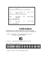
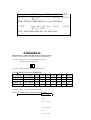
ADDENDUM(5V-1A VER.2.2A)
CN4
1
I
NOTE: ADD CN11 “TB-LED,” “CN10” & “CN4”
CN11
CN10
TB-LED PW-LED Keylock
Speaker
Reset
SU-LED
SU-SW HD-LED
NOTE: DELETE “HDD LOW LEVEL FORMAT” IN BIOS SETUP
39
ADDENDUM FOR 5V-1A VER.2.2
Intel® Pentium Processor Installation
CPU CLOCK
P54C 75 MHZ
P54C 90 MHZ
P54C 100 MHZ
P54C 120 MHZ
P54C 133 MHZ
P54C 150 MHZ
P54C 166 MHZ
P55C 166 MHZ
P54C 180 MHZ
P54C 200 MHZ
P55C 200 MHZ
P55C 233 MHZ
3.3V
3.3V
3.3V
3.3V
3.3V
3.3V
3.3V
2.8V/3.3V
3.3V
3.3V
2.8V/3.3V
2.8V/3.3V
SYS.
JCK1 JCK2 JCK3 JCK4 JBF0
JBF1
JBF2
CLOCK
50 MHZ 2-3
2-3
2-3
1-2 OPEN OPEN OPEN
60 MHZ 1-2
2-3
2-3
2-3 OPEN OPEN OPEN
66 MHZ 2-3
1-2
2-3
2-3 OPEN OPEN OPEN
60 MHZ 1-2
2-3
2-3
2-3 CLOSE OPEN OPEN
66 MHZ 2-3
1-2
2-3
2-3 CLOSE OPEN OPEN
60 MHZ 1-2
2-3
2-3
2-3 CLOSE CLOSE OPEN
66 MHZ 2-3
1-2
2-3
2-3 CLOSE CLOSE OPEN
66 MHZ 2-3
1-2
2-3
2-3 CLOSE CLOSE OPEN
60 MHZ 1-2
2-3
2-3
2-3 OPEN CLOSE OPEN
66 MHZ 2-3
1-2
2-3
2-3 OPEN CLOSE OPEN
66 MHZ 2-3
1-2
2-3
2-3 OPEN CLOSE OPEN
66 MHZ 2-3
1-2
2-3
2-3 OPEN OPEN OPEN
JPW1
JV1
1-2,5-6,7-8
1-2,5-6,7-8
1-2,5-6,7-8
1-2,5-6,7-8
1-2,5-6,7-8
1-2,5-6,7-8
1-2,5-6,7-8
7-8
1-2,5-6,7-8
1-2,5-6,7-8
7-8
7-8
OPEN
OPEN
OPEN
OPEN
OPEN
OPEN
OPEN
1-2,3-4
OPEN
OPEN
1-2,3-4
1-2,3-4
JBF2
JPW1
JV1
OPEN
OPEN
OPEN
OPEN
OPEN
OPEN
OPEN
OPEN
CLOSE
CLOSE
CLOSE
1-2,3-4,5-6,7-8
1-2,3-4,5-6,7-8
1-2,3-4,5-6,7-8
1-2,3-4,5-6,7-8
1-2,7-8
1-2,7-8
5-6,7-8
1-2,5-6,7-8
3-4
3-4
3-4
OPEN
OPEN
OPEN
OPEN
1-2,3-4
1-2,3-4
1-2,3-4
1-2,3-4
1-2,3-4
1-2,3-4
1-2,3-4
JV2
1-2
1-2
1-2
1-2
1-2
1-2
1-2
1-2
1-2
1-2
1-2
1-2
RATIO
1.5X
1.5X
1.5X
2X
2X
2.5X
2.5X
2.5X
3X
3X
3X
3.5X
AMD K5/K6/K6-2 Processor Installation
CPU CLOCK
K5-PR 75
3.52V
K5-PR 90/PR120 3.52V
K5-PR100/PR133 3.52V
K5-PR166 3.52V
K6-PR166 2.9V/3.3V
K6-PR200 2.9V/3.3V
K6-PR233 3.2V/3.3V
K6-PR233 3.3V/3.3V
K6-PR266 2.2V/3.3V
K6-PR300 2.2V/3.45V
K6-2 266 2.2V/3.3V
SYS.
JCK1 JCK2 JCK3 JCK4 JBF0
CLOCK
50 MHZ 2-3
2-3
2-3
1-2 OPEN
60 MHZ 1-2
2-3
2-3
2-3 OPEN
66 MHZ 2-3
1-2
2-3
2-3 OPEN
66 MHZ 2-3
1-2
2-3
2-3 CLOSE
66 MHZ 2-3
1-2
2-3
2-3 CLOSE
66 MHZ 2-3
1-2
2-3
2-3 OPEN
66 MHZ 2-3
1-2
2-3
2-3 OPEN
66 MHZ 2-3
1-2
2-3
2-3 OPEN
66 MHZ 2-3
1-2
2-3
2-3 CLOSE
66 MHZ 2-3
1-2
2-3
2-3 CLOSE
66 MHZ 2-3
1-2
2-3
2-3 CLOSE
JBF1
OPEN
OPEN
OPEN
CLOSE
CLOSE
CLOSE
OPEN
OPEN
OPEN
CLOSE
OPEN
JV2 RATIO
1-2
1-2
1-2
1-2
1-2
1-2
1-2
1-2
1-2
2-3
1-2
1.5X
1.5X
1.5X
2.5X
2.5X
3X
3.5X
3.5X
4X
4.5X
4X
Cyrix 6x86 Processor Installation
CPU CLOCK
P120+ M1 3.52V
P133+ M1 3.52V
P150+ M1 3.52V
P166+ M1 3.52V
P133+ 2.8V/3.3V 6X68L
P150 + 2.8V/3.3V 6X68L
P166+ 2.8V/3.3V 6X68L
P200+ 2.8V/3.3V 6X68L
MX PR 166 2.9V/3.3V
MX PR 200 2.9V/3.3V
MX PR 233 2.9V/3.3V
MII PR 300 2.9V/3.3V
SYS.
JCK1 JCK2 JCK3 JCK4 JBF0
JBF1
CLOCK
50 MHZ 2-3 2-3 2-3 1-2 CLOSE OPEN
55 MHZ 2-3 2-3 1-2 2-3 CLOSE OPEN
60 MHZ 1-2 2-3 2-3 2-3 CLOSE OPEN
66 MHZ 2-3 1-2 2-3 2-3 CLOSE OPEN
55 MHZ 2-3 2-3 1-2 2-3 CLOSE OPEN
60 MHZ 1-2 2-3 2-3 2-3 CLOSE OPEN
66 MHZ 2-3 1-2 2-3 2-3 CLOSE OPEN
75 MHZ 1-2 2-3 1-2 2-3 CLOSE OPEN
66 MHZ 2-3 1-2 2-3 2-3 CLOSE OPEN
75 MHZ 1-2 2-3 1-2 2-3 CLOSE OPEN
75 MHZ 1-2 2-3 1-2 2-3 CLOSE CLOSE
66 MHZ 2-3 1-2 2-3 2-3 OPEN OPEN
40
JBF2
JPW1
JV1
OPEN
OPEN
OPEN
OPEN
OPEN
OPEN
OPEN
OPEN
OPEN
OPEN
OPEN
OPEN
1-2,3-4,5-6,7-8
1-2,3-4,5-6,7-8
1-2,3-4,5-6,7-8
1-2,3-4,5-6,7-8
7-8
7-8
7-8
7-8
1-2,7-8
1-2,7-8
1-2,7-8
1-2,7-8
OPEN
OPEN
OPEN
OPEN
1-2,3-4
1-2,3-4
1-2,3-4
1-2,3-4
1-2,3-4
1-2,3-4
1-2,3-4
1-2,3-4
JV2
1-2
1-2
1-2
1-2
1-2
1-2
1-2
1-2
1-2
1-2
1-2
1-2
RATIO
2X
2X
2X
2X
2X
2X
2X
2X
2X
2X
2.5X
3.5X
Intel® Pentium Processor Installation
CPU CLOCK
P54C 75 MHZ
P54C 90 MHZ
P54C 100 MHZ
P54C 120 MHZ
P54C 133 MHZ
P54C 150 MHZ
P54C 166 MHZ
P55C 166 MHZ
P54C 180 MHZ
P54C 200 MHZ
P55C 200 MHZ
P55C 233 MHZ
3.3V
3.3V
3.3V
3.3V
3.3V
3.3V
3.3V
2.8V/3.3V
3.3V
3.3V
2.8V/3.3V
2.8V/3.3V
SYS.
JCK1 JCK2 JCK3 JCK4 JBF0
JBF1
JBF2
CLOCK
50 MHZ 2-3
2-3
2-3
1-2 OPEN OPEN OPEN
60 MHZ 1-2
2-3
2-3
2-3 OPEN OPEN OPEN
66 MHZ 2-3
1-2
2-3
2-3 OPEN OPEN OPEN
60 MHZ 1-2
2-3
2-3
2-3 CLOSE OPEN OPEN
66 MHZ 2-3
1-2
2-3
2-3 CLOSE OPEN OPEN
60 MHZ 1-2
2-3
2-3
2-3 CLOSE CLOSE OPEN
66 MHZ 2-3
1-2
2-3
2-3 CLOSE CLOSE OPEN
66 MHZ 2-3
1-2
2-3
2-3 CLOSE CLOSE OPEN
60 MHZ 1-2
2-3
2-3
2-3 OPEN CLOSE OPEN
66 MHZ 2-3
1-2
2-3
2-3 OPEN CLOSE OPEN
66 MHZ 2-3
1-2
2-3
2-3 OPEN CLOSE OPEN
66 MHZ 2-3
1-2
2-3
2-3 OPEN OPEN OPEN
JPW1
JV1
1-2,5-6,7-8
1-2,5-6,7-8
1-2,5-6,7-8
1-2,5-6,7-8
1-2,5-6,7-8
1-2,5-6,7-8
1-2,5-6,7-8
7-8
1-2,5-6,7-8
1-2,5-6,7-8
7-8
7-8
OPEN
OPEN
OPEN
OPEN
OPEN
OPEN
OPEN
1-2,3-4
OPEN
OPEN
1-2,3-4
1-2,3-4
JBF2
JPW1
JV1
OPEN
OPEN
OPEN
OPEN
OPEN
OPEN
OPEN
OPEN
CLOSE
CLOSE
CLOSE
1-2,3-4,5-6,7-8
1-2,3-4,5-6,7-8
1-2,3-4,5-6,7-8
1-2,3-4,5-6,7-8
1-2,7-8
1-2,7-8
5-6,7-8
1-2,5-6,7-8
3-4
3-4
3-4
OPEN
OPEN
OPEN
OPEN
1-2,3-4
1-2,3-4
1-2,3-4
1-2,3-4
1-2,3-4
1-2,3-4
1-2,3-4
JV2
1-2
1-2
1-2
1-2
1-2
1-2
1-2
1-2
1-2
1-2
1-2
1-2
RATIO
1.5X
1.5X
1.5X
2X
2X
2.5X
2.5X
2.5X
3X
3X
3X
3.5X
AMD K5/K6/K6-2 Processor Installation
CPU CLOCK
K5-PR 75
3.52V
K5-PR 90/PR120 3.52V
K5-PR100/PR133 3.52V
K5-PR166 3.52V
K6-PR166 2.9V/3.3V
K6-PR200 2.9V/3.3V
K6-PR233 3.2V/3.3V
K6-PR233 3.3V/3.3V
K6-PR266 2.2V/3.3V
K6-PR300 2.2V/3.45V
K6-2 266 2.2V/3.3V
SYS.
JCK1 JCK2 JCK3 JCK4 JBF0
CLOCK
50 MHZ 2-3
2-3
2-3
1-2 OPEN
60 MHZ 1-2
2-3
2-3
2-3 OPEN
66 MHZ 2-3
1-2
2-3
2-3 OPEN
66 MHZ 2-3
1-2
2-3
2-3 CLOSE
66 MHZ 2-3
1-2
2-3
2-3 CLOSE
66 MHZ 2-3
1-2
2-3
2-3 OPEN
66 MHZ 2-3
1-2
2-3
2-3 OPEN
66 MHZ 2-3
1-2
2-3
2-3 OPEN
66 MHZ 2-3
1-2
2-3
2-3 CLOSE
66 MHZ 2-3
1-2
2-3
2-3 CLOSE
66 MHZ 2-3
1-2
2-3
2-3 CLOSE
JBF1
OPEN
OPEN
OPEN
CLOSE
CLOSE
CLOSE
OPEN
OPEN
OPEN
CLOSE
OPEN
JV2 RATIO
1-2
1-2
1-2
1-2
1-2
1-2
1-2
1-2
1-2
2-3
1-2
1.5X
1.5X
1.5X
2.5X
2.5X
3X
3.5X
3.5X
4X
4.5X
4X
Cyrix 6x86 Processor Installation
CPU CLOCK
P120+ M1 3.52V
P133+ M1 3.52V
P150+ M1 3.52V
P166+ M1 3.52V
P133+ 2.8V/3.3V 6X68L
P150 + 2.8V/3.3V 6X68L
P166+ 2.8V/3.3V 6X68L
P200+ 2.8V/3.3V 6X68L
MX PR 166 2.9V/3.3V
MX PR 200 2.9V/3.3V
MX PR 233 2.9V/3.3V
SYS.
JCK1 JCK2 JCK3 JCK4 JBF0
JBF1
CLOCK
50 MHZ 2-3 2-3 2-3 1-2 CLOSE OPEN
55 MHZ 2-3 2-3 1-2 2-3 CLOSE OPEN
60 MHZ 1-2 2-3 2-3 2-3 CLOSE OPEN
66 MHZ 2-3 1-2 2-3 2-3 CLOSE OPEN
55 MHZ 2-3 2-3 1-2 2-3 CLOSE OPEN
60 MHZ 1-2 2-3 2-3 2-3 CLOSE OPEN
66 MHZ 2-3 1-2 2-3 2-3 CLOSE OPEN
75 MHZ 1-2 2-3 1-2 2-3 CLOSE OPEN
66 MHZ 2-3 1-2 2-3 2-3 CLOSE OPEN
75 MHZ 1-2 2-3 1-2 2-3 CLOSE OPEN
75 MHZ 1-2 2-3 1-2 2-3 CLOSE CLOSE
41
JBF2
JPW1
JV1
OPEN
OPEN
OPEN
OPEN
OPEN
OPEN
OPEN
OPEN
OPEN
OPEN
OPEN
1-2,3-4,5-6,7-8
1-2,3-4,5-6,7-8
1-2,3-4,5-6,7-8
1-2,3-4,5-6,7-8
7-8
7-8
7-8
7-8
1-2,7-8
1-2,7-8
1-2,7-8
OPEN
OPEN
OPEN
OPEN
1-2,3-4
1-2,3-4
1-2,3-4
1-2,3-4
1-2,3-4
1-2,3-4
1-2,3-4
JV2
1-2
1-2
1-2
1-2
1-2
1-2
1-2
1-2
1-2
1-2
1-2
RATIO
2X
2X
2X
2X
2X
2X
2X
2X
2X
2X
2.5X
MII PR 300 2.9V/3.3V
66 MHZ
2-3
1-2
2-3
2-3 OPEN
OPEN
OPEN
1-2,7-8
1-2,3-4
1-2
ADDENDUM (5V-1A ver. 2.2A)
Reg: case connector
TB-LED PW-LED Keylock
Speaker
Reset
SU-LED
SU-SW HD-LED
Reg: AMD® K6-2 300
CPU CLOCK
K6-2 300 2.2V/3.3V
SYS.
JCK1 JCK2 JCK3 JCK4 JBF0
JBF1
JBF2
CLOCK
66 MHZ 2-3
1-2
2-3
2-3 CLOSE CLOSE CLOSE
JPW1
JV1
3-4
1-2,3-4
JV2 RATIO
1-2
4.5X
(5V-1A ver. 2.2A)
:
TB-LED PW-LED Keylock
Speaker
Reset
SU-LED
SU-SW HD-LED
: AMD ® K6-2 300
CPU
K6-2 300 2.2/3.3V
JCK1 JCK2 JCK3 JCK4 JBF0
JBF1
JBF2
JPW1
66 MHZ 2-3 1-2
2-3
2-3
CLOSE CLOSE CLOSE 3-4
42
JV1 JV2
1-2, 3-4 1-2 4.5X
3.5X