1
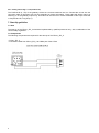
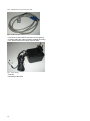
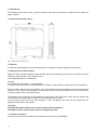
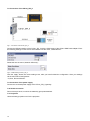
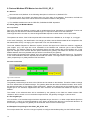
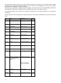
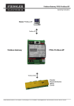
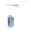
Version: 2014-01-24 CS121 SPI_II / BACS SPI_II User Manual Copyright Statement for Intellectual Property and Confidential Information The information contained in this manual is non-conditional and may be changed without due notice. Although Generex has attempted to provide accurate information within this document, Generex assumes no responsibility for the accuracy of this information. Generex shall not be liable for any indirect, special, consequential, or accidental damage including, without limitations, lost profits or revenues, costs of replacement goods, loss or damage to data arising out of the use of this document Generex the manufacturer of the BACS products undertakes no obligations with this information. The products that are described in this brochure are given on the sole basis of information to its channel partners for them to have a better understanding of the Generex products. Generex allows its channel partners to transfer information contained in this document to t hird persons, either staff within their own Company or their own customers, either electronically or mechanically, or by photocopies or similar means. Generex states that the content must not be altered or adapted in any way without written permission from Generex. It is agreed that all rights, title and interest in the Generex’s trademarks or trade names (whether or not registered) or goodwill from time to time of Generex or in any intellectual property right including without limitation any copyright, patents relating to the Products, shall remain the exclusive property of Generex. Generex will undertake to deal promptly with any complaints about the content of this document. Comments or complaints about the document should be addressed to Generex Systems GmbH. Copyright of the European Union is effective (Copyright EU). Copyright (c) 1995-2012 GENEREX GmbH, Hamburg, Germany. All rights reserved. Revision 2 History Date -001 Release 02/2010 -002 New Hardware Type 02/2010 -003 Polling from script version Rev. 002 09/2010 Table of Contents 1. Information of CE Marking of the Assembly Group 1.1 EU Directive EMV 1.2 Operating range 1.3 Assembling guideline 1.4 Mounting of the device 1.5 Operation at switch cabinets 2. Advices for the Manufacturer of Machines 2.1 Introduction 2.2 EU Directive Machines 3. Introduction 4. The Operating Modes of the Gateway 4.1 Data Exchange Mode 5. Functionality of the System 5.1 General explanation 5.2 Interfaces 5.3 Possible data lenghts 6. Hardware Connections, Switches and Diodes 6.1 Device marking 6.2 Connectors 6.2.1 Connectors to the external device (RS-Interface) 6.2.2 Connector power supply 6.2.3 ProfibusDP connector 6.2.4 Power supply 6.3 LED display 6.3.1 LED “(Bus) Power“ 6.3.2 LED “Bus“ 6.3.3 LED “(Bus) State“ 6.3.4 LED “Power“ 6.3.5 LED “State“ 6.3.6 LEDs 1 / 2 / 4 / 8 (Error No / Select ID) 6.4 Switches 6.4.1 Termination Rx 422 + Tx 422 (serial interface) 6.4.2 Coding switch S4 + S5 (serial interface) 6.4.3 Termination (Profibus) 6.4.4 Coding switch High + Low (Profibus-ID) 7. Start-Up guideline 7.1 Note 7.2 Components 7.3 Assembling 7.4 Scale drawing CS121_SPI_II 7.5 Start-up 7.6 Setting of the Profibus address 7.7 Profibus connection 7.8 Connection of the CS121_SPI_II 7.9 Connection of the power supply 7.10 Shield connection 7.11 Projection 8. Protocol Modbus-RTU Master into the CS121_SP_II 8.1 Advices 8.2 CS121_SPI_II as Modbus-Master 8.2.1 Preparation 8.2.2 Data construction 8.2.3 Communication action 8.3 The lenghts byte 8.4 Example of the polling for the CS121 values Rev. 002 8.5 Example of the polling for the CS121 values prior Rev. 002 9. Error Treatment 9.1 Error treatment by the CS121_SPI_II 10. Assembling Guideline 10.1 Assembling of the assembly group 10.1.1 Assembling 3 5 5 5 5 5 5 5 5 5 5 6 6 6 6 6 6 6 6 7 7 7 7 7 7 7 7 8 8 8 8 8 8 8 8 9 9 9 9 11 11 11 11 11 12 12 12 12 13 13 13 13 13 13 13 13 17 21 21 22 22 22 10.1.2 Dismantling 10.2 Wiring 10.2.1 Mounting technology 10.2.2 Power supply 10.2.3 Connection of the potential equalization 10.3 Communcation interface ProfibusDP 10.3.1 Bus wiring with copper cable 10.4 Wiring, shielding and activities against interfering voltage 10.4.1 General to the wiring 10.4.2 Shielding of cables 11. ProfibusDP 11.1 Description of the DPV1-/DPV2 functions 11.1.1 DPV1 11.1.2 DPV2 11.2 Display of the data in ProfibusDP 11.2.1 Configuration telegram 11.2.2 Diagnosis 11.2.3 Diagnosis into DPV1 11.2.4 Data exchange 12. Technical data 12.1 Device data 12.2 Interface data Appendix A Transmittal of a device B Figures 4 22 23 23 23 23 23 23 23 23 24 24 24 24 25 25 25 27 30 30 31 31 32 33 33 33 1. Information of CE Marking of the Assembly Group 1.1 EU Directive EMV For this assembly group is valid: Products, which bear the CE marking, accomplish the requirements of the EU Directive „Electromagnetical Compabitility“ and the specified harmonized european standards (EN). We can allocate the EU Declarations of Conformity at your desire. 1.2 Operating range The assembly groups are designed for the use into the industrial sector and accomplish the following requirements: Operating range Industry Requirement to Transient emissions Interference resistance EN 55011 Kl. A EN 61000-6-2 1.3 Assembling guideline The assembly group accomplishs the requirements, if you: 1. adhere to the assembling guidelines at installation and operation. 2. consider the following regulations at the mounting of the device and the operation at switch cabinets. 1.4 Mounting of the device It is required to install assembly groups into operating rooms or into closed housings (e.g. switch cabinets out of metal or plastic material). In addition it is required to ground the device and the switch cabinet or rather the tophat rail, where the assembly group was snapped on. 1.5 Operation at switch cabinets For the protection of the assembly groups, it is required that the personnel discharge themselves electrostatically, prior of the operation at the switch cabinets. 2. Advices for the Manufacturer of Machines 2.1 Introduction The assembly group CS121_SPI_II is not a machine pursuant the EU Directive „Machines“. Therefore no declaration of conformity is present for this assembly group. 2.2 EU Directive Machines The EU Directive „Machines“ regulates the requirements for a machine. Here the definition of a machine is the total of connected parts or appliances (see EN 292-1, section 3.1). The assembly group is a part of of the electrical equipment of a machine. It is required that the manufacturer of the machine has to be involved into the procedure of the declaration of conformity. 3. Introduction The assembly group CS121_SPI_II serves as adaptation of a serial interface at the ProfibusDP to EN 50 170. It is functioned as gateway in this case of application and operates as ProfibusDP slave. Every norm compliant master is able to operate with it. The assembly group consists essentially out of the following components: • • • • • • 5 Isolated RS485 interface to the ProfibusDP Profibus ASIC Microprocessor 89C51RD2 RAM and EPROM Optional isolated Serial interface (RS232, RS485 and RS422) to the external connected device 4. The Operating Modes of the Gateway 4.1 Data Exchange Mode The gateway has to be arranged into the data exchange mode, so that a data exchange is possible between the RS-side of the gateway and the field bus. This mode is always active, if the gateway is not to be arranged into configuration-, test- or debug mode. Into the data exchange mode the gateway will execute the recorded script. 5. Functionality of the System 5.1 General explanation Adapted from the ISO/OSO model, a communication can be partitioned into 7 layers (layer 1 to layer 7). The gateways of the CS121_SPI_II convert the layer 1 and layer 2 of a customized bus system (RS485 / RS232 / RS422) to the accordant field bus system. Layer 3 to layer 6 are empty, layer 7 will be converted pursuant chapter 8.3. 5.2 Interfaces The gateway is equipped with the interfaces RS232, RS422 and RS485. 5.3 Possible data lenghts See the possible data lenghts into the following table: Input data max. 244 Bytes variable: here Maximalwert Output data max. 244 Bytes variable: here Maximalwert Parameter 8 Bytes no user parameter * Configuration data max. 16 Bytes configuration dependent * Diagnosis a user diagnosis byte = Error code * max. 8 Bytes 6. Hardware Connections, Switches and Diodes 6.1 Device marking Fig. 1: Connection marking and termination Fig. 2: Front blind: Turn-switch, diodes and termination PB If the front blind will pop out, so this will have no effect to the function or quality of the device. You can just insert it. 6 6.2 Connectors 6.2.1 Connectors to the external device (RS-Interface) The serial interface is available at the upper side of the device. Pin-adjustment X1 (3pol. + 4pol. screw-connector) Pin Nr. 1 2 3 4 5 6 7 Name Rx 232 Tx 232 AP-GND Rx 422+ (485+) Rx 422- (485-) Tx 422+ (485+) Tx 422- (485-) Function Receive signal Transfer signal Application Ground Receive signal Receive signal Transfer signal Transfer signal For the operation at a 485 interface, it is required to connect the PINs with the marking „485-„. Also both PINS with the marking „485+“. 6.2.2 Connector power supply Pin-adjustment X2 (4pol. screw-connector, rear side, back) Pin Nr. Name Function 1 UB (Pwr) 10..33 Volt power supply / DC 2 0 V (Pwr) 0 Volt power supply / DC 6.2.3 ProfibusDP connector The connector (marking PROFIBUS) is at the front side of the device for the connection to the Profibus. Pin-adjustment (9pol. D-SUB socket) Pin Nr. 1 2 3 4 5 6 7 8 9 Name Shield Function B CNTR-P M5 P5 not inverting in-/output signal from Profibus control signal/repeater DGND, data ground 5 V power supply A inverting in-/output signal from Profibus 6.2.4 Power supply The device needs a 10-33 VDC power supply, which ensued via the 4pol. screw-connector at the bottom. Do not connect the devices of the series CS121_SPI_II with AC! 6.3 LED display The gateway CS121_SPI_II possesses about 9 LEDs with the following relevance: LED (Bus) Power LED Bus LED (Bus) State LED Power LED State LED 1 / 2 / 4 / 8 (Error No / Select ID) green red red/green green red/green green Power supply Profibus Profibus error State interface Profibus Power supply serial interface custom/common gateway error custom/common gateway error 6.3.1 LED “(Bus) Power“ This LED is connected to the power supply (potential separated) of the Profibus side directly. 6.3.2 LED “Bus“ This LED wil be actuated from the Profibus ASIC directly and will be off into the „Data Exchange“ mode. 7 6.3.3 LED “(Bus) State“ green shiny green flashing geen/red flashing red shiny Profibus into state data exchange Gateway awaiting configuration data of the Profibus Gateway awaiting Profibus parameter data Common Profibus error 6.3.4 LED “Power“ This LED is connected to the power supply (optional potential separated) of the serial interface (RS232/RS422/RS485) directly. 6.3.5 LED “State“ green shiny green flashing green/red flashing red shiny red flashing controllable via script controllable via script controllable via script common gateway error, controllable via script CS121_SPI_II is into configuration/test mode, controllable via script 6.3.6 LEDs 1 / 2 / 4 / 8 (Error No / Select ID) If these 4 LEDs are flashing and the „state“ LED is shining red, the error number will be binary-coded displayed, pursuant of the table into the chapter „error treatment“. 6.4 Switches The gateway possesses 7 switches with the following functions: Termination Rx 422 Termination Tx 422 Coding switch S4 Coding switch S5 Termination (Profibus) Coding switch High Coding switch Low switchable Rx 422-terminating resistance for the serial interface switchable Tx 422- or RS485- terminating resistance for the serial interface ID High for serial interface, default „0“ ID Low for serial interface, default „0“ switchable ProfibusDP terminating resistance ProfibusDP ID (High Byte) ProfibusDP ID (Low Byte) 6.4.1 Termination Rx 422 + Tx 422 (serial interface) If the gateway will be operating as first or rather last device into a RS485 bus or RS422, it is required to implement a bus termination. Therefor the termination switch has to be into the position ON. The integrated resistance (150 ) into the gateway will be activated. In any other case, the termination switch has to be into the position OFF. You will find further information about the bus termination into the common RS485 literature. Please note, if the integrated resistance will be used, that therewith a pull-down resistance (390 ) to ground and a pull-up resistance to VCC (390 ) will be enabled. At RS485 the Tx 422 switch has to be into position ON only. The Rx 422 switch has to be into position OFF. 6.4.2 Coding switch S4 + S5 (serial interface) These two switches can be read out via the script command « Get (RS_Switch, Destination »). The value can be used for other functions. This value will be read in at switching on of the gateway or rather after the execution of the script command. The switch setting « EE » (test mode) and « FF » (config mode) are not available at the RS422- or RS485 operation. 6.4.3 Termination (Profibus) If the gateway will be operating as first or last device into a ProfibusDP, it is required to implement a bus termination. Therfor the activation of a bus terminating resistance into the connector or the integrated resistance (220 ) into the gateway is required. For that the termination switch has to be into the position ON. In any other case, the termination switch has to be into the position OFF. You will find further information about the bus termination into the common Profibus literature. Advice: Please detach the bus connector and adjust the switch into the desired position carefully, to enable/disable the bus termination. 8 6.4.4 Coding switch High + Low (Profibus-ID) The Profibus-ID (0…7D) of the gateway will be set via these switches into hex. Please take a look into the conversion table of decimal to hex into the appendix for further information. These value will will be read in at switching on of the gateway unique only. This value can be read out or rather evaluated via the script command « Get (field bus-ID, LongTemp »). 7. Start-Up guideline 7.1 Note The start-up of the CS121_SPI_II should be implemented by qualified personnel only, with consideration of the current safety regulation! 7.2 Components The following components are required for the start-up of the CS121_SPI_II: • CS121_SPI_II • Connection cable from CS121_SPI_II to COM2 port of the CS121 9 Fig. 3: PIN adjustment of the connection cable Fig. 4: COM2 Connection cable • Connector for the Profibus connection to the gateway • Profibus cable (this cable is already installed generally) • 12V, 500mA VDC power supply (at most 30V) Fig. 5: Power Supply • GSD file • Operating instructions 10 7.3 Assembling The assembly group CS121_SPI_II got the protection class IP20 and therefore is adapted for the usage into switch cabinets. 7.4 Scale drawing CS121_SPI_II Fig. 6: Scale drawing CS121_SPI_II 7.5 Start-up To assure a proper operating of the assembly group, it is required to note the following at the start-up: 7.6 Setting of the Profibus address Approach: Set the Profibus address at the field bus side of the assembly group at both turn-switches with the marking "Profibus-ID High“ and “Profibus-ID Low“. This setting takes place in hexadecimal. Example: The Profibus-ID is 26 decimal = 1A hexadecimal. It is required to put the switch „Profibus-ID High“ into position 1 and the switch „Profibus-ID Low“ into position A. If the turn-switch will be put into the position „7E“ (=126) at Profibus side, the gateway will work with a Profibus address, which is stored into the EPROM. This address is 126 into the delivery status and can be changed from a Profibus master only via the Profibus itself. The address 126 is reserved into the Profibus for this purpose, that means that a slave with this address will never be able to exchange data, but rather can be configured with a new ID. If the turn-switch will be put at a value between 0...125, the gateway will work with this Profibus-ID. An adjustment via master is not possible. Attention: The defined Profibus address has to match with the projected address! The address will be read-in at the switch on of the gateway only! 7.7 Profibus connection Connect the device with the Profibus at the interface with the marking „PROFIBUS“. 11 7.8 Connection of the CS121_SPI_II Fig. 7: Connection of the CS121_SPI_II Connect the RS232 interface of the CS121_SPI_II with the COM 2 port of the CS121 SNMP web-adapter. Enter the following settings via the CS121 web-interface into the menu „COM2 & AUX“: Parameter into the menu „Network & Security“: Fig. 8: COM 2 Settings CS121_SPI_II Click the „Apply“ button into the according menu, after you have finished the configuration. Save your settings via the menu Save Configuration“ „Save, Exit and Reboot“. 7.9 Connection of the power supply Connect the enclosed power supply at the CS121_SPI_II gateway. 7.10 Shield connection Ground the top-hat rail, on which the assembly group was attached. 7.11 Projection Use an arbitrary projection tool for the projection. 12 8. Protocol Modbus-RTU Master into the CS121_SP_II 8.1 Advices We used the word „Modbus“ in the following description in reference to „Modbus-RTU“. The terms „Input“ and „Output“ are always seen out of the sight of the gateway. That means, the field bus input data are the data, which will be send from the field bus master to the gateway. The available modules are into the GSD-File „DAGW2079.GSD“ deposited. 8.2 CS121_SPI_II as Modbus-Master 8.2.1 Preparation Due to the fact that the Modbus is working with a variable data format, dependent to the desired function and data lenght, but the field bus needs a fixed data lenght, it is required to select it into the GSD-File. This lenght should be choosen so, that the longest Modbus request or rather answer can be processed. The operator can select, if the fiel bus requests will be forwarded to the Modbus at „on change“ or „on trigger“. In the mode „Changing“, the identification of a changing is visible, that the field bus data will be compared to the last transmission and by a changing of a request will occur over the Modbus only. The mode „Modbus Request On Demand“ requires, that the first byte into the field bus contains a triggerbyte (see chapter 10.5). This byte will not be forwarded to the Modbus and conduces just to start a Modbus transmission. The gateway observes this triggerbyte always and will transfer data to the Modbus only, if this byte has changed. In the reverse direction (to the field bus) the gateway will transfer the amount of received Modbus dataset; after every dataset this byte will be incremented by the gateway. Is the lenghts byte activated (see chapter 10.6), the gateway will transfer the specified bytes only. The amount of the received Modbus data are deposited at the field bus master. The lenght refers to the bytes „address“ to „data“ (respectively incl.) always without CRC checksum. 8.2.2 Data construction Fig. 9: Data construction 8.2.3 Communication action The gateway retains always as slave to the field bus and as master to the Modbus. Therefore a data exchange has to be started from the field bus always. The gateway takes the data from the field bus master, which has to be arranged pursuant to the chapter „Data construction“, detects the valid lenght of the Modbus data, if the lenghts byte is not activated, supplemented the CRC checksum and transfers this dataset as request to the Modbus. The answer of the selected slave will be transfered by the gateway to the field bus master without CRC checksum. Will no answer occur in the defined response time, the gateway will trigger a „timeout error“. 8.3 The lenghts byte You can define, if the transfer-lenght should be deposited as byte into the in- or rather output dataset (field bus lenghts byte -> active). It will be transfered so much bytes, as defined into this byte in the transfer direction. At the receiving of a telegram, the gateway will be insert the amount of the received signs. 8.4 Example of the polling for the CS121_SPI_II Rev. 002 From script version Rev. 002 it is no longer required, to configure the Modbus polling into the Profibus master. 13 You will find the revision number of your CS121_SPI_II as button onto the device. The revision number 002 will be delivered from september 2010 by default. The older revisions will be addressed on another way, please take a look into chapter 8.5 for further information. The CS121_SPI_II gateway is polling by itself accordingly, cyclical to the CS121. At a valid Modbus answer the UPS data will be send with an additional byte and Modbus error byte to the Profibus cyclical. It is required to select into the module “64 words I/O (consistent) into the Profibus master out of the GSD file UGIC3218”. For the allocation of the UPS data to the transferred bytes on the Profibus, please take a look into the following table. Byte Name Description Lenght 1 Counter Increase at valid answer 1 Byte 2 Modbus Error Byte Data valid if 0x00 only 1 Byte 3+4 OUTP0WER0 Outpower Phase 1 % 1 Word 5+6 OUTP0WER1 Outpower Phase 2 % 1 Word 7+8 OUTP0WER2 Outpower Phase 3 % 1 Word 9 + 10 BATTCAP Battery Capacity % 1 Word 11 + 12 INVOLT0 Input Voltage Phase 1 V 1 Word 13 + 14 INVOLT1 Input Voltage Phase 2 V 1 Word 15 + 16 INVOLT2 Input Voltage Phase 3 V 1 Word 17 + 18 TEMPDEG Temperature C° 1 Word 19 + 20 AUTONOMTIME Autonomy Time minutes 1 Word 21 + 22 STATUS (e. g. UPS normal = “4”, Powerfail = “12”, Battery test running = “68”, Bypass = “5” ) UPS Status (ASCII HEX) 1 Word Please note UPSMAN status bytes table below 23 + 24 BATTVOLT Battery Voltage V 1 Word 25 + 26 INFREQ0 Input Frequency Hz Phase 1 1 Word 14 27 + 28 INFREQ1 Input Frequency Hz Phase 2 1 Word 29 + 30 INFREQ2 Input Frequency Hz Phase 3 1 Word 31 + 32 CNT_PF Powerfail Counter 1 Word 33 + 34 Alarm Battery Bad 1 = active; 0 = not active 1 Word 35 + 36 Alarm: On Battery 1 = active; 0 = not active 1 Word 37 + 38 Alarm: Battery Low 1 = active; 0 = not active 1 Word 39 + 40 Alarm: Battery Depleted 1 = active; 0 = not active 1 Word 41 + 42 Alarm: Over temperature 1 = active; 0 = not active 1 Word 43 + 44 Alarm: Input Bad 1 = active; 0 = not active 1 Word 45 + 46 Alarm: Output Bad 1 = active; 0 = not active 1 Word 47 + 48 Alarm: Output Overload 1 = active; 0 = not active 1 Word 49 + 50 Alarm: On Bypass 1 = active; 0 = not active 1 Word 51 + 52 Alarm: Bypass Bad 1 = active; 0 = not active 1 Word 53 + 54 Alarm: Output Off as requested. 1 = active; 0 = not active 1 Word 55 + 56 Alarm: UPS Off as requested. 1 = active; 0 = not active 1 Word 57 + 58 Alarm: Charger Failed 1 = active; 0 = not active 1 Word 59 + 60 Alarm: UPS Output Off 1 = active; 0 = not active 1 Word 61 + 62 Alarm: UPS System Off 1 = active; 0 = not active 1 Word 63 + 64 Alarm: Fan Failure 1 = active; 0 = not active 1 Word 65 + 66 Alarm: fuse failure 1 = active; 0 = not active 1 Word 15 67 + 68 Alarm: general fault 1 = active; 0 = not active 1 Word 69 + 70 Alarm: diagnose test failed 1 = active; 0 = not active 1 Word 71 + 72 Alarm: communication lost 1 = active; 0 = not active 1 Word 73 + 74 Alarm: awaiting power 1 = active; 0 = not active 1 Word 75 + 76 Alarm: shutdown pending 1 = active; 0 = not active 1 Word 77 + 78 Alarm: shutdown imminent 1 = active; 0 = not active 1 Word 79 + 80 Alarm: test in progress 1 = active; 0 = not active 1 Word 81 + 82 AUX Port 1 1 = active (high) 0 = not active (low) 1 Word 83 + 84 AUX Port 2 1 = active (high) 0 = not active (low) 1 Word 85 + 86 AUX Port 3 1 = active (high) 0 = not active (low) 1 Word 87 + 88 AUX Port 4 1 = active (high) 0 = not active (low) 1 Word 89 + 90 BACS State see table below BACS_State 1 Word 91 + 92 BACS State 1 see table below BACS_State_1 1 Word 93 + 94 BACS_Alarms see table below BACS_Alarms 1 Word UPS Status Hex-Value Dec-Value Description UPS_SB_BYPASS_MODE 0x0001 1 power piped thru UPS_SB_SHUTDOWN 0x0002 2 shutdown ups UPS_SB_OUTPUT_ACT 0x0004 4 inverter on = UPS OK UPS_SB_BACKUP_MODE 0x0008 8 battery power UPS_SB_BATTERY_LOW 0x0010 16 low battery err UPS_SB_OVER_TEMP 0x0020 32 over temp err UPS_SB_TEST_ACT 0x0040 64 test in progress UPS_SB_INPUT_HIGH 0x0080 128 over power err 16 UPS Status Hex-Value Dec-Value Description UPS_SB_OUTPUT_HIGH 0x0100 256 over load err UPS_SB_INVERTER_FAILURE 0x0200 512 Inverter error UPS_SB_BATTERY_BAD 0x0400 1024 Battery error UPS_SB_ECO_MODE 0x0800 2048 eco - bypass UPS_SB_INVERTER_WARN 0x1000 4096 eco - bypass UPS_SB_UPS_FAILED 0x2000 8192 prser flag UPS_SB_COMM_LOST 0x4000 16384 for snmp UPS_SB_DVG_ALARM 0x8000 32768 SiteManager/SiteMonitor BACS_State BACS_STATE_RUNNING BACS_STATE_CONNECTED BACS_STATE_MODULE_LOST BACS_STATE_DISCHARGING BACS_STATE_CHARGING BACS_STATE_DISCHARGING_STOPPED BACS_STATE_FLOAT_CHARGING BACS_STATE_EQUALIZING BACS_STATE_SYSTEM_FAILURE BACS_STATE_VOLTAGE_OUTOFRANGE BACS_STATE_TEMPERATURE_OUTOFRANGE BACS_STATE_RESISTOR_OUTOFRANGE BACS_STATE_MODULE_ADDRESSING BACS_STATE_MODULE_SEARCHING BACS_STATE_MODULE_INITIALIZING BACS_STATE_MODULE_POLLING 0x0001 0x0002 0x0004 0x0008 0x0010 0x0020 0x0040 0x0080 0x0100 0x0200 0x0400 0x0800 0x1000 0x2000 0x4000 0x8000 BACS_State_1 BACS_STATE_GENERAL_ALARM BACS_STATE_VOLTAGE_DIFF_HIGH BACS_STATE_BATTERY_BREAKER_OPEN 0x0001 0x0002 0x0004 BACS_Alarms BACS_ALARM_GENERAL_ALARM BACS_ALARM_COMMUNICATION_LOST BACS_ALARM_VOLTAGE_HIGH BACS_ALARM_VOLTAGE_LOW BACS_ALARM_TEMPERATURE_HIGH BACS_ALARM_TEMPERATURE_LOW BACS_ALARM_RESISTOR_HIGH BACS_ALARM_RESISTOR_LOW BACS_ALARM_EQUALIZING_ERR BACS_ALARM_VOLTAGE_WARN_HIGH BACS_ALARM_VOLTAGE_WARN_LOW BACS_ALARM_TEMPERATURE_WARN_HIGH BACS_ALARM_TEMPERATURE_WARN_LOW BACS_ALARM_RESISTOR_WARN_HIGH BACS_ALARM_RESISTOR_WARN_LOW BACS_ALARM_MODREV_INCOMPATIBLE 0x0001 0x0002 0x0004 0x0008 0x0010 0x0020 0x0040 0x0080 0x0100 0x0200 0x0400 0x0800 0x1000 0x2000 0x4000 0x8000 8.5 Example of the polling for the CS121 values prior Rev. 002 The CS121_SPI_II before Rev. 002 was delivered until August 2010. The CS121 provides the Modbus functions Holdings Register (0x03) and Input Register (0x04). Some customized versions provide write functions too, which can be withdrawn out of the Modbus specification. 17 For the polling of the Modbus addresses 100 – 142, please use the available modules of the GSD file „DAGW2079.GSD“. It is required to use several modules for the polling of all values. The usage of several modules is required, because the gateway will transfer the field bus requests to the CS121 only, if the request is different to the previous one. Default UPS adress description Note: “Type U/S”: this defines whether the answer has an algebraic sign (math. +/-) or not. U means “unsigned”. S means “signed”, this answer may be positive or negative. Adress Type Function Name 18 Description Lenght 100 U 3/4 OUTP0WER0 Outpower Phase 1% 1 101 U 3/4 OUTP0WER1 Outpower Phase 2% 1 102 U 3/4 OUTP0WER2 Outpower Phase 3% 1 103 U 3/4 BATTCAP Battery Capacity % 1 104 S 3/4 INVOLT0 Input Voltage Phase 1 V 1 105 S 3/4 INVOLT1 Input Voltage Phase 2 V 1 106 S 3/4 INVOLT2 Input Voltage Phase 3 V 1 107 S 3/4 TEMPDEG Temperature C° 1 108 S 3/4 AUTONOMTIME Autonomy Time minutes 1 109 U 3/4 STATUS (e. g. UPS normal = “4”, Powerfail = “12”, Battery test running = “68”, Bypass = “5” ) UPS Status (ASCII HEX) 1 110 S 3/4 BATTVOLT Battery Voltage V 1 111 U 3/4 INFREQ0 Input Frequency Hz Phase 1 1 112 U 3/4 INFREQ1 Input Frequency Hz Phase 2 1 113 U 3/4 INFREQ2 Input Frequency Hz Phase 3 1 114 U 3/4 CNT_PF Powerfail Counter 1 Please note UPSMAN status bytes table below 19 115 U 3/4 Alarm Battery Bad 1 = active; 0 = not active 1 116 U 3/4 Alarm: On Battery 1 = active; 0 = not active 1 117 U 3/4 Alarm: Battery Low 1 = active; 0 = not active 1 118 U 3/4 Alarm: Battery Depleted 1 = active; 0 = not active 1 119 U 3/4 Alarm: Over temperature 1 = active; 0 = not active 1 120 U 3/4 Alarm: Input Bad 1 = active; 0 = not active 1 121 U 3/4 Alarm: Output Bad 1 = active; 0 = not active 1 122 U 3/4 Alarm: Output Overload 1 = active; 0 = not active 1 123 U 3/4 Alarm: On Bypass 1 = active; 0 = not active 1 124 U 3/4 Alarm: Bypass Bad 1 = active; 0 = not active 1 125 U 3/4 Alarm: Output Off as requested. 1 = active; 0 = not active 1 126 U 3/4 Alarm: UPS Off as requested. 1 = active; 0 = not active 1 127 U 3/4 Alarm: Charger Failed 1 = active; 0 = not active 1 128 U 3/4 Alarm: UPS Output Off 1 = active; 0 = not active 1 129 U 3/4 Alarm: UPS System Off 1 = active; 0 = not active 1 130 U 3/4 Alarm: Fan Failure 1 = active; 0 = not active 1 131 U 3/4 Alarm: fuse failure 1 = active; 0 = not active 1 132 U 3/4 Alarm: general fault 1 = active; 0 = not active 1 133 U 3/4 Alarm: diagnose test failed 1 = active; 0 = not active 1 134 U 3/4 Alarm: communication lost 1 = active; 0 = not active 1 135 U 3/4 Alarm: awaiting power 1 = active; 0 = not active 1 136 U 3/4 Alarm: shutdown pending 1 = active; 0 = not active 1 137 U 3/4 Alarm: shutdown imminent 1 = active; 0 = not active 1 138 U 3/4 Alarm: test in progress 1 = active; 0 = not active 1 139 U 3/4 AUX Port 1 1 = active (high) 1 0 = not active (low) 140 U 3/4 AUX Port 2 1 = active (high) 1 0 = not active (low) 141 U 3/4 AUX Port 3 1 = active (high) 1 0 = not active (low) 142 U 3/4 AUX Port 4 1 = active (high) 1 0 = not active (low) 20 143 U 3/4 Sensormanager/SMTCOM sensor 1 Analog value 1 144 U 3/4 Sensormanager/SMTHCOM Analog value sensor 2 1 145 U 3/4 Sensormanager sensor 3 Analog value 1 146 U 3/4 Sensormanager sensor 4 Analog value 1 147 U 3/4 Sensormanager sensor 5 Analog value 1 148 U 3/4 Sensormanager sensor 6 Analog value 1 149 U 3/4 Sensormanager sensor 7 Analog value 1 150 U 3/4 Sensormanager sensor 8 Analog value 1 Example: Request address 100 – 113 with module -> 16 words I/O (consistently) 0x01 0x04 0x00 0x64 0x00 0x12 0x00 0x00 0x00 0x00 0x00 0x00 0x00 0x00 0x00 0x00 0x00 0x00 0x00 0x00 0x00 0x00 0x00 0x00 0x00 0x00 0x00 0x00 0x00 0x00 0x00 0x00 The first 6 bytes contain the request, the other bytes will be filled up with 0x00. The checksum calculation will be arranged from the CS121_SPI_II automatically and attached. Byte 1 = Slave address, is always 1 at the CS121 Byte 2 = Modbus Function Code, the CS121 provides 0x03 or 0x04 Byte 3 = High byte of the start address, first measuring value, the CS121 starts with 0x64 (100 dez.) Byte 4 = Low byte of the start address, first measuring value, the CS121 starts 0x64 (100 dez.) Byte 5 = High byte of the amount of the requested values, dependent of the used module of the GSD file Byte 6 = Low byte of the amount of the requested values, dependent of the used module of the GSD file Answer 0x01 0x04 0x12 0x00 0x63 0x00 0x58 0x00 0x4D 0x00 0x64 0x00 0xE6 0x00 0xE7 0x00 0xE8 0x00 0x17 0x00 0x0F 0x00 0x04 0x00 0xE9 0x00 0x32 0x00 0x00 0x00 0x00 0x00 Attention: Please note at the amount of the polling values, that the input buffer will not overflow at the answer! Byte 1 = Slave address Byte 2 = Modbus Function Code Byte 3 = Amount of the following data words Byte 4 = High byte of the first value of the CS121 (100 dez.) Byte 5 = High byte of the first value of the CS121 (100 dez.) Byte 6 = High byte of the second value of the CS121 (101 dez.) Byte 7 = High byte of the second value of the CS121 (101 dez.) etc. It is required to define a loop into the Profibus master programming, that the content of the request will change. E.g. request: Modbus address 100 – 113, request: Modbus address 114 – 126 or rather further, if more values are essential. 9. Error Treatment 9.1 Error treatment by the CS121_SPI_II Detects the gateway an error, so it will be signalized via the LED state (red shining). Coincident the error number will be displayed pursuant of the following table via the LEDs « Error No ». You can distinguish two error categories : Heavy errors (1-5) : It is required to reset the gateway. If the error will occur again, it is required to exchange it and to send it for reparation. Warnings (6-15) : These warnings will be displayed for one minute for your information only and will be reset automatically, but if these warnings will occur frequently, please advise the customer service. The flashing frequency is 0,5 Hertz at custom errors. The error will be displayed as long as the « Set Warning Time » was defined. The displays are not valid into configuration mode and for internal purpose only. LED8 LED4 LED2 LED1 Error number/ID Error description 0 0 0 0 0 Reserved 0 0 0 1 1 Hardware error 0 0 1 0 2 EPROM error 21 0 0 1 1 3 Internal storage error 0 1 0 0 4 Field bus Hardware error or wrong field bus ID 0 1 0 1 5 Script error 0 1 1 0 6 Reserved 0 1 1 1 7 RS send buffer overflow 1 0 0 0 8 RS receiving buffer overflow 1 0 0 1 9 RS timeout 1 0 1 0 10 Common field bus error 1 0 1 1 11 Parity- or frame check error 1 1 0 0 12 Reserved 1 1 0 1 13 Field bus configuration error 1 1 1 0 14 Field bus data buffer overflow 1 1 1 1 15 Reserved 10. Assembling Guideline 10.1 Assembling of the assembly group The assembly group with the at most dimensions (23x111x117mm WxHxT) was developed for the switch cabinet insertion (IP20) and can be attached onto a top-hat rail (EN50022) only. 10.1.1 Assembling • The assembly group should be fitted from above into the top-hat rail and pivotted to bottom until the assembly group is engaged. • You can string other assembly groups left and/or right beside your assembly group. • The top-hat rail has to be connected to the potential equalization rail of the switch cabinet. It is required, that the connection wire has a cross section of at least 10qmm. 10.1.2 Dismantling • At first it is required to stake out the power supply- and signal cables. • Afterwards press the assembly group above and pan it out of the top-hat rail. Vertical assembling It is also possible to mount the top-hat rail vertical, so that the assembly group will be mounted 90°C turned. 22 10.2 Wiring 10.2.1 Mounting technology You can appoint the following mounting technologies: • Default screw-/plug connection (power supply + RS) • 9pol. D-SUB connector (ProfibusDP) a) Every point of attachment is clampable at the default screw terminal. Allowed cross sections of the cable: • Flexible cable with wire end ferrule: 1 x 0,25 ... 1,5 mm² • Massive cable: 1 x 0,25 ... 1,5 mm² • Locking torque: 0,5 ... 0,8 Nm b) The pluggable terminal strip is acombination out of a default screw terminal and a plug connector. c) The 9pol. D-SUB connector is secured via 2 screws with “4-40-UNC“- thread. Use a screwdriver (3,5mm), locking torque: 0,2 ...0,4 Nm. 10.2.2 Power supply The device should be supplied with 10..33VDC. • Connect the power supply to the 4pol. plug screw terminal according the marking of the device. 10.2.3 Connection of the potential equalization The connection to the potential equalization will happen during the attachment onto the top-hat rail. 10.3 Communcation interface ProfibusDP 10.3.1 Bus wiring with copper cable This interface is at the top of the assembly group in the form of a 9pol. D-SUB socket at the front side of the device. • Plug the Profibus connector onto the D-SUB socket with the marking "ProfibusDP". • Tighten the securing screws of the connector with a screwdriver. • If the gateway will be operating as first or rather last device into a Profibus, it is required to implement a bus termination. Therefor the termination switch has to be into the position ON. In any other case, the termination switch has to be into the position OFF. 10.4 Wiring, shielding and activities against interfering voltage This chapter describes the wiring of bus-, signal- and supply cables with the goal to assure an EMV-like assembling. 10.4.1 General to the wiring - inside and outside of cabinets For an EMV-like assembling of cables, it is appropriate to arrange the cables into the following groups and to lay them separate. 23 Group A: • shielded bus- and data cables, e.g. for ProfibusDP, RS232, printers etc. • shielded analog cables • unshielded cables for DC 60 V • unshielded cables for AC 25 V • Coaxial transmission line for monitors Group B: • unshielded cables for DC 60 and • unshielded cables for AC 24 V and 400 V 400 V Group C: • unshielded cables for DC > 400 V See the following table for the requirements. Group A Group B Group C Group A 1 2 3 Group B 2 1 3 Group C 3 3 1 Table: Cable regulations dependent of the combination of cable groups: 1) Cables can be layed together in bundles or wireways. 2) Cables have to be layed into separate bundles or wireways (without minimum distance). 3) Cables have to be layed into separate bundles or wireways into cabinets, but have to be layed into separate wireways with at least 10cm distance into facilities. 10.4.2 Shielding of cables The shielding is an activity for the weakening of magnetical or electrical interfering fields. Error currents onto the shielding of cables will be derived to the ground via the shield rail. So that these error currents will not become a disturbance source, a connection with low impedance to the grounding conductor is essential. Use cables with braid preferably only. The coverage tightness should be more than 80%. Avoid cables with shielding foil, because the foil can be damaged during the attachment and a decrease of the shielding effect would be present. Generally the shieldings of cables should be always disposed both-sided, but you just achieve an absorbability of lower frequencies. A one-sided shielding might be better, if: • the laying of a potential equalization cable can not be done • analog signals (some mV or rather mA) will be transferred • shielding foils will be used Use always metallized connectors for data cables with serial couplings. Attach the shielding of the data cable at the connector cabinet. An equalization current can be flow over the both-sided connected shielding by potential differencies between the grounding points. In this case, please lay an additonally potential equalization cable. Please note the following by the shielding conditioning: • Use metal cable clamps for the attachment of the braid. The clamps should surround the shielding extensive and execute close contact. • Lay the shielding right after the entrance of the cable into the cabinet onto a shielding-rail. Carry the shielding until the assembly group on, but do not reissue it! ! 11. ProfibusDP 11.1 Description of the DPV1-/DPV2 functions 11.1.1 DPV1 The DPV1 extension persists out of the following functions: 1. Acyclic data exchange with class1-master (e.g. SPS) This function is optional for a DPV1 slave only. Our gateways support these functions by default. The class1master can read and write data from the slave acyclic via this function. These data will be widespread into the gateway from the script. The channel for the acyclic data exchange will be set during the parameterization. 2. Acyclic data exchange with class2-master (e.g. control pane) This function is optional for a DPV1 slave only. Our gateways support these functions by default. The class1master can read and write data from the slave acyclic via this function. These data will be widespread into the 24 gateway from the script. The channel for the acyclic data exchange will be established prior of the exchange and closed afterwards. 3. Alarmhandling The alarms are optional too. If activated, they replace the device specific diagnosis. Our gateways does not support alarms yet. Every DPV1 slave has to support the extended parameterization, because it will be defined into octet 8 of the parameter telegram, if a DPV0 or a DPV1 is connected. You can use a DPV1 slave at a DPV0 master, if the DPV1 functions are disabled. 11.1.2 DPV2 The DPV2 extension persists out of the following functions: 1. Isochron Mode (IsoM) The isochron mode is the synchronous behaviour of a bus system. This function is optional for a DPV2 slave and can be activated via the GSD file. Our gateway does not support the mode yet. 2. Data Exchange Broadcast (DxB) The data exchange broadcast is the communication between slaves (lateral transport). This function is optional for a DPV2 slave and can be activated via the GSD file. Our gateway supports the function of the „Publisher“ (transfer data to other slaves) only. The function „Subscriber“ (receive data from other slaves) is not supported yet 3. Up- und Download These function is for a DPV2 slave too, but is not supported of our gateway yet. 4. Time Snchronization (Time stamp) These function is for a DPV2 slave too, but is not supported of our gateway yet. 5. Redundancy concept These function is for a DPV2 slave too, but is not supported of our gateway yet. 11.2 Display of the data in ProfibusDP Every norm compliant ProfibusDP master can exchange data with the gateway. You can use very simple master activations, because of the data establishment 11.2.1 Configuration telegram The master has to send a configuration telegram to the according slave after the parameterization. The slave will get the information of the lenght of the in-/output data via the configuration telegram. If the user has set the flag „lenght byte“ into the CS121_SPI_II, are these the at most data lenghts, otherwise the actual lenghts. The configuration telegram will be composed into the projection tool, where the user can indicate the address range, in which the reference data are discarded. You can write up to 16 bytes or rather words into one octet of the data unit (DU). You can combine the in/outputs in an octet, if they got the same format. Otherwise you can use as many octets as you want to use for different bytes/words. Detect the assembly group during the overhaul, that the maximum in-/outputdata lenghts were exceeded, the wrong configuration will be reported to the master at future polling diagnosis. It is not ready for the data traffic. Octet 1 0 Configuration byte 1 25 Configuration byte x Octet 2 26 0 Construction of an octet into the configuration telegram Data lenght 00 = 1 byte/word 15 = 16 bytes/words In-/Output 00 = Specified identification format 01 = Input 10 = Output 11 = In-/Output 0 = Byte, 1 = Word 0 = Consistent via byte/word 1 = Consistency overall lenght 11.2.2 Diagnosis Diagnosis data are prior-ranking data. The gateway generates an external diagnosis, if an internal error was detected. Display of the messages into the external diagnosis byte: The diagnosis information of a DP slave persists out of default diagnosis information (6 bytes) and an user specified diagnosis information (error number). Telegram for the diagnosis request: Octet 1 0 Diagnosis station not existent (master setting) Diagnosis station not_ready: Slave is not ready for data exchange Diagnosis cfg_Fault: Configuration data are not matching Diagnosis ext_diag: Slave got external diagnosis data Diagnosis not supported: Requested function is not supported by the slave Diagnosis invalid_slave_response (slave setting at 0 steady) Diagnosis prm_fault: Wrong parameterization (identification number etc.) 27 Diagnosis master_lock (master setting): Slave was parameterized from other master Diagnosis Prm_req: New slave parameterization is required Diagnosis Stat_diag: Statical diagnosis (byte diag-bits) Steady at 1 Diagnosis WD_ON: Approach monitoring active Diagnosis freeze_mode: Freeze command received Sync_mode: Sync command received reserved Diagnosis deactivated (master setting) 28 Octet 2 0 reserved Diagnosis ext_overflow Octet 3 0 Diagnosis master_add: Master address after parameterization (FF without parameterization) Octet 4 0 Ident number high byte Octet 5 0 Ident number low byte Octet 6 0 External diagnosis: Head data lenght Octet 7 0 CS121_SPI_II error number Octet 8 29 0 11.2.3 Diagnosis into DPV1 The external diagnosis from DPV0 (old PB) is used in a different way from DPV1. Alarms and state messages will be transferred by DPV1. It was required to adjust the DPV1, because we have transferred the gateway error numbers into the external diagnosis. We added the 3 bytes „0x81, 0x00, 0x00“ prior of the proper error message, to be compatible to the DPV1 master. Therefore the DPV1 master is able to detect our gateway error as state message. Therefore a different display of our gateway-error is shown into the PB: At DPV0 the error-number will be transferred as 1 byte external diagnosis. If DPV1 is enabled via the GSD file into the gateway, the error-number will be transferred as 1 byte state message. In this case, that DPV1 is enbled and a master is connected, which does not support the the alarms and state mesages, the gateway-error-number will appear as 4 byte external diagnosis. The 4th byte contains the errornumber, so you can ignore the other 3 bytes (0x81, 0x00, 0x00). 11.2.4 Data exchange After the master will detect into the diagnosis, that the slave is ready for the data exchange, the master will send data exchange telegrams. The data of the in- or rather output direction will be discarded from the master into the address range, which was stated at the projection or it is required, that the control program gets/allocates the data via specified components. 30 12. Technical data 12.1 Device data Please take a look into the following table for the technical data of the assembly group. Nr. Parameter Data Explanation 1 Site Switch cabinet Top-hat rail assembling 2 Safety class IP20 Contaminant and water protection IEC 529 (DIN 40050) 4 Durability 10 years 5 Dimensions of the housing 23 x 111 x 117 mm W x H x D (incl. Screw terminals) 23 x 100 x 117 mm (without them) 6 Fitting position any 7 Weight 130 g 8 Operating temperature -20ºC ... +70ºC 9 Storage/transport temperature -40ºC ... +70ºC 10 Operating air pressure bei Transport 11 Altitude of site 795 hPa ... 1080hPa 660 hPa ... 1080hPa 2000 m 4000 m Without reservations With reservations Ambient temperature 40ºC 12 Rel. humidity Max. 80 % Not condensating 14 External power supply 10...33V DC Default power supply (DIN 19240) 15 Current consumption at 24VDC Typ. 120 mA max 150 mA At 10,8V: typ. 350 mA 16 Power supply at the Profibus interface 5V DC / max. 50 mA (Max. 50 mA at < 30°C ambient temperature) 17 Reverse battery protection yes Device does not work 18 Differential protection yes 19 Overload protection Poly-Switch 20 Subvoltage detection 9V DC 21 Powerfailure bridging 5 ms 31 Thermal fuse Device is working 12.2 Interface data Interface marking, physical interface ProfibusDP RS232-C RS485/RS422 Nr. RS485 RS232-C RS485/RS422 1 Norm 2 Transmission method EIA default symmetric asynchronous serial half duplex DIN 66020 asymmetric asynchronous serial full duplex EIA default symmetric asynchronous serial half duplex/ full duplex at RS422 Difference signal Gauge Difference signal 3 Transmission method 4 Attendance: - Sender - Receiver 5 Kabel lenght: - maximal Master / Slave 32 32 1200 m Master / Slave 1 1 15 m -baudrate 93,75 kBd 1200 m no 187,5 kBd 1000 m 500 kBd 400 m 1,5 MBd 200 m 1,5 MBd 100 m dependent 6 Bus-Topology 7 Data rate: - maximal Line 12 Mbit/s -Default 9,6 kBit/s 19,2 kBit/s 93,75 kBit/s 187,5 kBit/s 500 kBit/s 1,5 Mbit/s 3 MBit/s 6 MBit/s 12 Mbit/s values 8 Sender: - Stress 54 -max. voltage - 7 V ... 12 V -Signal without 5 V stress 1,5 V -Signal with stress 9 Receiver: -Input 12 resistance - 7 V ... 12 V -max. input 0,2 V signal - Sensitivity 10 Transmission range - 0,2 ... + 0,2 V (SPACE): - voltage 0 gauge Master / Slave 32 32 1200 m 93,75 kBd 1200 m 312, kBd 500 m 625 kBd 250 m Point to point 120 kBit/s 2,4 k/B 4,8 k/B 9,6 kBit/s 19,2 kBit/s 38,4 kBit/s Line 625 kBaud 2,4 kBit/s 4,8 kBit/s 9,6 kBit/s 19,2 kBit/s 57,6 kB 312,5 kB 625 kB 3 ... 7 k 25 V 15 V 5V 54 - 7 V ... 12 V 5V 1,5 V 3 ... 7 15 V 3V 12 - 7 V ... 12 V 0,2 V + 3 ... + 15 V 0 - 0,2 ... + 0,2 V 0 - 3 ... –15 V 1 + 1,5 ... +5 V 1 - Logic gauge 11 Transmission break (MARK): -voltage gauge + 1,5 ... +5 V 1 - Logic gauge 32 Appendix A Transmittal of a device At the transmittal of a device, it is required to send us a broad description of the malfunction. We need the following details: • Which error-number was displayed? • What is the value of the power supply (±0,5V) with connected gateway? • What were the last activities at the device (programming, error at switch on etc.)? If you have any queries, send us an email to [email protected]. B Figures Fig. 1: Connection marking and termination .......................................................................... 6 Fig. 2: Front blind: Turn-switch, diodes and termination PB ................................................. 6 Fig. 3: PIN adjustment of the connection cable .................................................................. 10 Fig. 4: COM2 Connection cable........................................................................................... 10 Fig. 5: Power Supply ............................................................................................................ 10 Fig. 6: Scale drawing CS121_SPI_II ................................................................................... 11 Fig. 7: Connection of the CS121_SPI_II ............................................................................. 12 Fig. 8: COM 2 Settings CS121_SPI_II ................................................................................ 12 Fig. 9: Data construction ....................................................................................................... 13 33