1
Copyright Warning & Restrictions
The copyright law of the United States (Title 17, United
States Code) governs the making of photocopies or other
reproductions of copyrighted material.
Under certain conditions specified in the law, libraries and
archives are authorized to furnish a photocopy or other
reproduction. One of these specified conditions is that the
photocopy or reproduction is not to be “used for any
purpose other than private study, scholarship, or research.”
If a, user makes a request for, or later uses, a photocopy or
reproduction for purposes in excess of “fair use” that user
may be liable for copyright infringement,
This institution reserves the right to refuse to accept a
copying order if, in its judgment, fulfillment of the order
would involve violation of copyright law.
Please Note: The author retains the copyright while the
New Jersey Institute of Technology reserves the right to
distribute this thesis or dissertation
Printing note: If you do not wish to print this page, then select
“Pages from: first page # to: last page #” on the print dialog screen
The Van Houten library has removed some of the
personal information and all signatures from the
approval page and biographical sketches of theses
and dissertations in order to protect the identity of
NJIT graduates and faculty.
ABSTRACT
GRAPHICAL USER INTERFACE FOR THE DSP:
USING TEXAS INSTRUMENTS TMS320C31 AND LABVIEW
by
Tahir Nazir
Digital Signal Processors (DSP's) have become very popular due to their ease
of operation, economic value, adaptability and availability. However, the development environments for the DSP are still the archaic Assembly and C language
programming. It is tedious, error prone and time consuming to develop and use DSP
applications using these compared to Graphical User Interface development tools if
available. In the modern age programming is very heavily done in object oriented
graphical languages like the Visual C++ and Visual Basic. Windows also gives a
good graphical user interface.
LABVIEW with its readily available ensemble of good analysis, programming
and development libraries and engineering tools was a good candidate. G programming
also gives ease of operation and relative economy in programming time, along with
good capabilities for hardware interfacing.
We have used Code Interface Node programmed in C language act as a bridge
between the LabVIEW and DSP and then carrying out the analysis in the LabVIEW
and using the DSP for collecting of data. The complete DSP control and monitoring
is carried out by the LabVIEW along with acquisition of data collected by the DSP.
The real world interface and analog to digital conversion is carried out by
the DSP and LabVIEW is used to analyze and present the data in a more user
friendly and graphical manner. The Use of LabVIEW has significantly reduced the
time required to carry out a simple test, by eliminating the need to use different
platforms to develop and execute the DSP program, and then collect data, and
finally to analyze the data.
GRAPHICAL USER INTERFACE FOR THE DSP:
USING TEXAS INSTRUMENTS TMS320C31 AND LABVIEW
by
Tahir Nazir
A Thesis
Submitted to the Faculty of
New Jersey Institute of Technology
in Partial Fulfillment of the Requirements for the Degree of
Master of Science in Electrical Engineering
Department of Electrical and Computer Engineering
May 1999
APPROVAL PAGE
GRAPHICAL USER INTERFACE FOR THE DSP:
USING TEXAS INSTRUMENTS TMS320C31 AND LABVIEW
Tahir Nazir
Dr. Timothy N. Chang, Thesis Advisor Associate Professor of Electrical Engineering, NJIT
Date
Dr. Marshall Kuo, Committee Member Professor of Electrical and Computer Engineering, NJIT
Date
Dr. Dao-Chuan Douglas Hung, Committee Member Associate Professor of Computer & Information Science, NJIT
Date
BIOGRAPHICAL SKETCH
Author:
Tahir Nazir
Degree:
Master of Science in Electrical Engineering
Date:
May 1999
Undergraduate and Graduate Education:
• Master of Science in Electrical Engineering,
New Jersey Institute of Technology, Newark, NJ, 1999
• Bachelor of Science in Electrical Engineering,
University of Engineering and Technology, Lahore, Pakistan, 1991
Major:
Electrical Engineering
To my family, friends and teachers
v
ACKNOWLEDGMENT
I would like to express my deepest appreciation and respect for Dr. Timothy N.
Chang, who not only served as my research supervisor, providing valuable and
countless resources, insight, and intuition, but also constantly gave me support,
encouragement, and reassurance. Special thanks to Dr. Marshal Kuo, and Dr. DaoChuan douglas Hung for actively participating in my committee.
Special thanks to Xuemei Sun, Vincent Pappano, Robin Nikfar, Hamid Ghods,
Bhaskar Dani, and many graduate students in the NJIT Electrical and Computer
Engineering department. Finally, I would like to thank the NIST ATP Grant
number 70NANB5H1092 for Precision Optoelectronics Assemply, for extending
financial support for this thesis, and also the NJIT for their financial support.
vi
TABLE OF CONTENTS
Chapter
Page
1 INTRODUCTION 1
1.1 Objective
1
1.2 TI TMS320C31 DSP
1
1.3 LabVIEW 1
1.4 Organization of Thesis
3
2 GRAPHICAL USER INTERFACE
4
2.1 Life Cycle of Software Development
4
2.2 GUI Development 4
2.3 GUI Implementation
5
2.4 Our GUI Structure
6
2.4.1 An Example of Our GUI 7
3 LABVIEW 9
3.1 G Programming
9
3.2 Code Interface Nodes 10
3.3 Graphs 12
3.4 Exec Function
12
3.5 Fast Fourier Transform 12
3.6 Using LabVIEW for Our System 13
3.6.1 The CIN for Our Example 16
4 TEXAS INSTRUMENTS TMS320C31 DSP 21
4.1 TI TMS320 Family 21
4.2 The Delanco Spry Board 22
4.3 The TMS320C31 Digital Signal Processor
23
4.4 Initialization 24
vii
Page
Chapter
4.5 DAC Usage
26
4.6 ADC Usage
27
4.7 Sampling Rate Determination
28
4.8 Runtime Sampling Rate Determination
4.9 Data Exchange between the PC and the DSP Card
29
30
31
5 THE PLANT (PZT) 5.1
PZT Ceramics Manufacturing Process 31
5.2
Advantages of Piezoelectric Positioning Systems 32
5.3
Displacement of Piezo Actuators 33
5.4
Considerations for PZT Usage 33
5.4.1 Mechanical Considerations 33
5.4.2 Electrical Considerations
34
5.4.3 Temperature Effects 35
Our Plant 35
6 IMPLEMENTATION 37
5.5
6.1
The DSP Block 37
6.1.1 The Front Panel 37
6.1.2 The Block Diagram 39
6.1.3 The CIN
39
6.1.4 The DSP Program 40
6.2 Hysteresis with Dither 6.2.1 The Front Panel
40
40
6.2.2 The Block Diagram 42
6.2.3 The CIN 43
6.2.4 The DSP Program 44
6.3 Range of PZT Displacement 44
6.3.1 The Front Panel 44
vi"
Chapter
Page
6.3.2 The Block Diagram 46
6.3.3 The CIN 47
6.3.4 The DSP Program 47
6.4 Resonant Frequency Determination 48
6.4.1 The Front Panel 49
6.4.2 The Block Diagram 50
6.4.3 The CIN 51
6.4.4 The DSP Program 51
6.5 PI Control Application 51
6.5.1 The Front Panel 52
6.5.2 The Block Diagram 54
6.5.3 The CIN 54
6.5.4 The DSP Program 55
7 CONCLUSION 7.1
56
Dithering
58
7.2 PI Completely Programmed in LabVIEW 60
7.3 Drawing a Circle with PZT 62
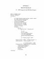
APPENDIX A THE BLOCK DIAGRAMS 64
APPENDIX B THE CINS 71
APPENDIX C THE DSP PROGRAMS 89
ix
LIST OF FIGURES
Figure
Page
1.1
The Block diagram representation of our system 2
2.1
The Block diagram of data flow. 6
3.1
Block Diagram depicting LabVIEW VI structure 10
3.2
The Block diagram of the case true Hysteresis 14
3.3
The Block diagram of the case false Hysteresis 15
3.4
The Block diagram of the input output
19
4.1
TMS320C31 Architecture 22
4.2
Synchronization to TCLK
28
4.3
Successive Read and Write Events 29
5.1
The Block diagram of our plant 34
6.1
The Front Panel of the DSP Block 38
6.2
The Front Panel of the Hysteresis program. 41
6.3
The Front Panel of the PZT Range 45
6.4
The Front Panel of the Resonance Frequency 49
6.5
The Front Panel of the Proportional Integral program 53
7.1
The Block diagram of data flow
57
7.2
Dithering in the X-axis of Plant 58
7.3
Dithering in the Y-axis of Plant 59
7.4
The PI control system completely programmed in LabVIEW 61
7.5
Block Diagram of PI control system completely programmed in LabVIEW 61
7.6
The Two PI control system 62
7.7
The output from PZT as a circle 63
A.1 The Block diagram of the case true DSP Block 65
A.2 The Block diagram of the case false DSP Block 65
Figure
Page
A.3 The Block diagram of the case true Hysteresis 66
A.4 The Block diagram of the case false Hysteresis 66
A.5 The Block diagram of the case true range of displacement 67
A.6 The Block diagram of the case false range of displacement 67
A.7 The Block diagram of the case true Resonance Frequency 68
A.8 The Block diagram of the case false Resonance Frequency 68
A.9 The Second Block diagram of the case true Resonance Frequency 69
A.10 The Block diagram of the case true Proportional Integral Control 69
A.11 The Block diagram of the case false Proportional Integral Control 70
xi
CHAPTER 1
INTRODUCTION
1.1 Objective
The objective of this thesis is to present the application of LabVIEW as a graphical
User interface (GUI) for the Digital Signal Processor. The LabVIEW version 5 was
used to carry out G language implementation of user interface. Code Interface Nodes
(CIN's) were used to exchange necessary data with the DSP. The DSP programming
was carried out in C language.
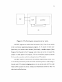
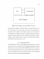
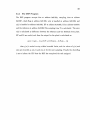
1.2 TI TMS320C31 DSP
The TI TMS320 family of Digital signal Processors combines the flexibility of high
speed controller with the numerical capability of an array processor. Thus an
impressive and economical alternative to VLSI and multichip bit-slice processors
for signal processing. TMS320 family offers both Fixed point and Floating point
DSP generations.
The Dalanco SPRY mode'_
data acquisition and signal_ processing board was
used as the housing of the DSP. This board provides us with two D/A converters
and four A/D converters. The relationship is expressed in Fig 1.1
1.3 LabVIEW
LabVIEW is a program development environment, it is different from other program
development environments for it uses graphical programming language rather than
text base language. LabVIEW is a general purpose programming system with
extensive libraries of functions for any programming task. LabVIEW includes
libraries for data acquisition, GPIB and serial instrument control, data analysis,
data presentation, and data storage.
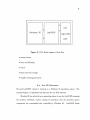
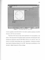
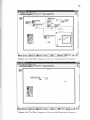
1
2
Figure 1.1 The Block diagram representation of our system.
LabVIEW programs are called virtual instruments (VIs). These VIs are similar
to the conventional programing language programs. A VI consists of three interlinked items, the interactive user interface (Front Panel), a dataflow diagram (Block
Diagram) that basically is the G language source code, and an icon to connect the
program to other high level VI programs. The icon works like a graphics parameter
list to provide connection and data exchange between VI programs.
LabVIEW adheres to and promotes the modular programming concept. Thus
we can develop an hierarchy of VIs and subVIs which each perform a task leading to
the end result. This makes debugging easier as we can execute each subVI by itself.
These subVls can also be used as a library and recalled and included in other VIs
which need similar functions.
3
G is easy to use graphical data flow programming language on which LabVIEW
is based. Scientific calculations, process monitoring and control, test and measurement
and a wide variety of applications can be developed in G.
1.4 Organization of Thesis
Chapter 2 of this thesis discusses the Graphical User Interface programing, and
concepts involved in such a task.
Chapter 3 discusses the LabVIEW development environment and the functions
used for our purposes. It explains mainly the different VIs in LabVIEW which were
used in our development of the GUI for DSP, and also some relevant discussion on
the CIN programming environment.
Chapter 4 discusses the TI TMS320 family of the DSPs and the Delanco SPRY
-rode' 3'_ 0 board we have used to perform our tasks.
Chapter 5 discusses the plant used for our work. We used PZTs as our test
subject for the application. Experiments to carry out studying of the PZT behaviour
were implemented using the LabVIEW and DSP working in tandem. Four experiments were mainly implemented to study the hysteresis characteristics of the PZT.
To find out the range of displacement of the PZT, leading to a measure of the scale of
PZT displacement to applied voltage. The plant used for our testing is also included
in this chapter.
Chapter 6 discusses the actual implementation of the experiments. It
covers discussions on considerations for the front panel design, the Block diagram
programming, the Code Interface Node programing and the DSP programs.
Finally in chapter 7, the conclusion of this work along with future directions
for research are provided.
CHAPTER 2
GRAPHICAL USER INTERFACE
2.1 Life Cycle of Software Development
The software development life-cycle approach has evolved over the years to a
structured approach from a waterfall model. The structured development may
include survey, analysis, design, implementation, acceptance test, quality assurance,
user documentation, final installation, and interactions between these activities.
Survey includes feasibility study and the study of the possible approaches
towards solving the issue. The System analysis has the purpose of providing
guidelines as to user and user activities. To develop user profiles, the analysis looks
at the users frequency of operation, computer skills, and general capabilities as to
the system.
Software design activity consists of decomposing the system into smaller easily
manageable sub systems. For GUI applications, adopting a dialog independent
software would require partitioning the system into GUI, and application functional
core subsystem. The subsystems can then be developed separately.
Implementation activity involves actual coding and integration of the subsystems
into a complete functional system. Testing can be started once the complete system
has been implemented. A test plan is developed with a set of exercises for the
system to perform. These exercises verify that the system performs to the desired
specifications and requirements.
2.2 GUI Development
User role is very dominant in the success of the GUI systems. We prioritize classes,
identify concurrent classes, and prioritize the task scenarios in the task model. We
consider the system level design for error prevention and recovery behaviour. The
results of analysis activities may need revision with time based on new findings. Task
4
5
model is revised to verify that the new finding don't need redesign of the task model.
We then map our user interface to style specific GUI designs. We identify common
interaction models. We attempt to retain the similarity of operations as much as
possible between different layers of application.
2.3 GUI Implementation
System is decomposed for implementation. There can be different approaches of
decomposition like:
• Functional decomposition
• Data flow decomposition
• Entity relationship decomposition
• Object oriented decomposition
The subsystems based on any of the decomposition models are all interconnected in some fashion. These interactions influence the runtime dynamics of
the system. Each of the decomposition may employ more than one interfacing
mechanism. Some of the basic interfacing mechanisms worth mentioning are:
• Sequential procedural call
• Message passing
• Event Responses
A GUI application consumes extensive graphical resources. The performance
depends on the following:
• Windows
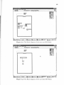
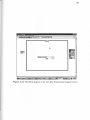
6
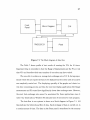
Figure 2.1 The Block diagram of data flow.
• mouse pointer
• Icons and Bitmaps
• Colors
• Fonts and Text strings
• Graphic drawing primitives
2.4 Our GUI Structure
We used LabVIEW version 5 running on a Windows 95 operating system. The
attached Figure 2.1 represents the data flow for our GUI software.
Windows 95 was selected as an operating system to run the LabVIEW meaning
the monitor, keyboard, mouse, timing of operations and all operating system
components are commanded and controlled by Windows 95. LabVIEW hands
7
over all it needs to display at monitor to Windows 95, and receives all keyboard and
mouse instructions from Windows 95.
The systems functionality is decomposed between LabVIEW, CIN, and DSP,
The DSP mainly interfaces to the physical plant through DACs, and ADCs, it collects
and performs some data manipulations and stores the data in the memory locations.
The CIN accesses these memory locations directly using the C language commands
outp, outpw, inp and inpw
which write or read data from the ports as specified in these commands.The format
for these commands is:
outp(Address, Value)
variable=inp(Address)
The output commands writes the data of the variable in position Value at the address
in the Address position. The input commands need a variable in which the read value
from the Address is to be stored.
LabVIEW exchanges the data with the CIN by references and as handles and
then processes and displays the data after further analysis or manipulation.
Windows 95 is not a realtime operating system and thus applications running
on this operating system cannot be real time. The Windows 95 allocates time slots
to each function active at a particular instant of time. The next time slot can be
awarded at any instant without relationship to the applications previous time slot.
Meaning that the same routine might run for a few milliseconds in one second or not
at all during a whole second. Depending on the priorities decided by Windows 95
operating system.
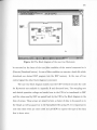
2.4.1 An Example of Our GUI
As an example let us discuss the development of one of our GUI interfaces with the
user. The survey part of our development life cycle is that we need an experiment
8
to determine the hysteresis characteristics of a plant. Study and analysis of our
problem reveals that we would like to control the sampling rate of the DSP while
performing the experiment and thus put an integer sampling rate control on our
screen. We would also like to control the applied voltage range for which the DSP
will perform the Hysteresis test. Our DSP can deliver upto ± 5 volts, hence a floating
point control for voltage is also placed on the screen. We also determine to give the
operator the capability to Download the program of DSP into its memory or to
execute the program already in the DSP memory.
We also need some feedback to be given to the user, and display the results.
Two forms of displaying the results are selected:
• Graphically
• As data displays
Graphically the data of the test is displayed in the form of an XY graph
displaying the relationship between the output voltage and the displacement of the
system. Output voltage is used for X-axis and displacement for Y-axis. In addition
the array of data received by the LabVIEW is also displayed in the form of two array
displays, so the exact value of the graph points can be read directly from these data
displays. It is also realized that the user might need to save the test results as a
reference for a later date, therefore the program also asks the user if he wishes to
save the data in the form of a spreadsheet file. The Front panel of the system is
displayed in Figure 6.1.
In addition to these developed graphical interfaces, LabVIEW also gives the
user some commands like the run, continuous run, stop and pause buttons. The user
can also change the screen as to personal needs.
CHAPTER 3
LABVIEW
3.1 G Programming
G is the programming language of LabVIEW. G is a general purpose programming
language with extensive libraries of functions for any programming task. G includes
libraries for data acquisition, GPIB and serial communications, data analysis, data
presentation, and data storage. Conventional program debugging tools are also
included so we can set break-points, animate the execution to see the data processing
and passage, as well as single step through the program to trap exact locations of
errors and for easier debugging.
However, G differs from other languages in that it has graphical interface with
the user rather than a text based interface. G programs are called Virtual instruments
due to their appearance and performance as imitating instruments. VI are similar
to functions of other programming languages.
A VI consists of three parts the user interface for human users, the icon
connections for embedding the VI as a subVl, and its source code in the form of
a wired Block Diagram. This relationship is further elaborated in Figure 3.1.
With these features G makes use of the concept of modular programming.
Distributing the tasks into subVls which collectively perform the desired task in the
block diagram (program) of the main VI.
We can also print our program documentation directly from the LabVIEW. We
can print the active window as well as a complete set of documentation. The print
documentation feature offers us a number of printing options and also a number of
printing destinations.
Another unique feature provided by the LabVIEW is the performance profiler
tool. This tool informs us where our application is spending time and the memory
it is using. This information is invaluable to identify the hotspots of our application
9
10
Figure 3.1 Block Diagram depicting LabVIEW VI structure
and to optimize our program. This feature informs us the total time spent by our
VI, the time spent by our subVls, number of runs for the VI, average amount of
time spent by the VI, Shortest and the longest time spent by our VI, Time spent
on executing the block diagram, time spent on updating the front panel interfaces,
time spent in drawing the front panel of the VI. Memory information is provided for
average bytes used, minimum bytes used, maximum bytes used, average, maximum
and minimum memory blocks used by our VI.
3.2 Code Interface Nodes
A Code Interface Node (CIN) is a block diagram node associated with a section of
source code written in a conventional text based programming language. We compile
and link the code to form executable CIN, LabVIEW calls the CIN as another of
its functions passing parameters to the node and accepting the data provided by the
node. CIN are geared for use with code or specific uses which can be accomplished
more easily using the conventional programming language.
11
CINs execute synchronously, meaning all other LabVIEW functions are
disabled. However LabVIEW monitors the keyboard, menus and may allow other
applications to execute depending on the operating system. CIN object code takes
control of the processes that LabVIEW ignores keyboard events, menu clicks, and
other diagrams.
A CIN appears as an icon with input and output terminals. The terminals are
associated with data in the Node source code and block diagram. LabVIEW calls the
code and passes the specified data. The interface for CINs and external subroutines
supports a variety of compilers.
Using CIN involves following steps:
• Place the CIN on block diagram.
• Create the necessary input output connections.
• Create a C source code.
• Compile the source code.
• Link the code to CIN.
LabVIEW passes data by reference to the CIN. LabVIEW passes numeric data
types to CINs by passing a pointer to the data as an argument. LabVIEW stores
Boolean in memory as 16-bit integers, and passes them same as numeric. Cluster
is passed by passing a pointer to a structure containing the elements of the cluster.
LabVIEW passes array by handle. LabVIEW also provides some functions to use
the handle properly.
12
3.3 Graphs
There are three types of graphs supported by LabVIEW:
• XY Graph
• Waveform graph
• Intensity graph
There are two type of charts supported by LabVIEW:
• Waveform Chart
• Intensity Chart
Each of these graphs and charts accept data of several types. We can customize
the appearance of the graph like putting grids, background and graph colors, label
and line type etc. We can also scale our graph to display the scaled data.The intensity
graph/chart displays three dimensional data in two dimensions.
3.4 Exec Function
It is a special function in the communications block and runs an executable file.
3.5 Fast Fourier Transform
Fast Fourier Transform is used to give frequency domain representation of data.
LabVIEW uses the Discrete Fourier Transform (DFT).
For a sampling frequency of
fa Hz, then the time interval between the samples
13
for k 0,1,2„ N — 1
A/ is known as the frequency resolution. To increase the resolution we can
increase the number of samples or decrease the sampling frequency.
Direct implementation of DFT requires N 2 complex operations for N samples.
However when the size of sequence is power of 2,
N = form = 1,2,3 Implementation of DFT becomes quite faster and is referred to as Fast Fourier
Transform. LabVIEW gives us two types of FFTs, Real FFT and Complex FFT.
3.6 Using LabVIEW for Our System
We discussed the development of the LabVIEW front Panel of Hysteresis testing
program in chapter 2, let us continue with the same example LabVIEW's Front
Panel Design Toolbox gave us the different Controls and Indicators these could have
been connected to the icon thus providing capability of our Hysteresis test VI to
serve as a subVl to other VIs. However, we chose not to do so, our icon just depicts
graphically a hysteresis plot.
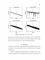
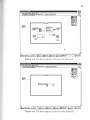
The Block diagram of the hysteresis VI is shown in Figure 3.2 and 3.3.
Basically we have made a case structure which decides which block diagram will
14
Figure 3.2 The Block diagram of the case true Hysteresis
be executed on the bases .of the true/false condition of the control connected to it
(Execute/Download button). In case of false condition we execute a batch file which
downloads our desired DSP program into the DSP memory. In the case of true
control signal the other block diagram is executed.
The case true block diagram mainly runs the eIN VI which executes the code
for Hysteresis test available in Appendix B and discussed later, The sampling rate
and desired operation voltage are handed over to the eIN to be transferred to DSP
and the values read by DSP are passed back by the eIN to the Block diagram in the
form of arrays. These arrays are joined to form a cluster of data to be passed on to
the Graph as well as passed on to the Spreadsheet file saving VI. It is important to
note that these wires are color coded by Lab VIEW to express the type of the data
flow in these wires.
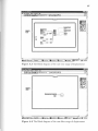
15
'01"
~--~-
Figure 3.3 The Block diagram of the case false Hysteresis
The diagram should be read left to right. The junction of two or more wires
executes when all data required is available to the input of the junction. Example is
the multiplication symbol executes only when both multiplicants are avai lable at its
input terminal.
The graphic symbols for the different indicators and controls also show the
type of data in abbreviation, e.g. 132 for 32 bit integer and DBL for double precision
floating point variables etc.
The Block Diagram screen of LabVIEW also gives the user some additional
debugging tools like the single step, show each execution and complete the execution
button on the top control panel of the screen. The run, continuous run, stop and
pause buttons are also available to the user. This allows us to check the data flow
and the execution sequence of our block diagram for troubleshooting purposes.
16
3.6.1 The CIN for Our Example
LabVIEW provides us with a header file extcode.h, that contains typedefs associating
LabVIEWs own unambiguous data types like intl6 for 16 bit integer type. This
header also defines some constants and types whose definitions may conflict with the
definitions of the systems header files. The names of the CIN routines are defined in
the header file with words CIN MgErr, it defines the word CIN as either Pascal or
nothing, depending on the platform. On PC the standard_ C calling conventions are
used. The MgrErr data type is a LabVIEW data type that corresponds to a set of
error codes that the manager routines return.
In our CIN the stdio.h, math.h, and conio.h header files are also included to use
the specific commands used in the CIN source code. The Type TD1 is also defined
as a handle which consists of an integer variable dimSize defining the number of
elements in the array and arg 1 the actual memory storage of the data elements.
These elements can each be accessed by arg 1 [i] where i is the element number in
array.
LabVIEW passes two pointers *Sampling _Rate, and *voltage and reads two
handles DSP _Input, and DS P _Output from the CIN. The main body of the CIN
starts with defining the variables which will be used by the CIN program to exchange
and manipulate the data between LabVIEW and DSP. The defined variables also
include the addresses in the DSP memory which the program will access. These
addresses are defined in Hex format.
The DSP is put to go or program execution mode by reading from port 0x306.
It is important to note that the memory is shared between the DSP and the PC.
The variable numDims defines dimensions of array.
Function NumericArrayResize is used to resize the data handle. This function
also accounts for alignment issues. It does not set the array dimension field. The
usage is:
17
Table 3.1 Constants for the typecode argument in NumericArrayResize function
The variable typecode describes the data type for the array that we want to
resize. The header file extcode.h has defined constants for this argument shown in
Table 3.1
The variable numDims describes the number of dimensions in the data
structure to which the handle refers. Thus, if the handle refers to a two-dimensional
array, you pass a value of 2 for numDims.
The variable *dataHP of extcode.h defined type UHandle is a pointer to the
Handle we want to resize.
The variable totalNewSize gives the NumericArrayResize the new number of
elements to which the the handle should refer. For a unidimensional array of 5
elements we pass 5. For a two-dimensional array of two rows by three columns we
pass 6.
Caution and care needs to be taken in the use of NumericArrayResize
function because LabVIEW allocates memory array for the CIN and in case of
18
any misalignment or differences in the way data is handled and manipulated by
LabVIEW or CIN can cause LabVIEW to cause system fault and be shutdown by
Windows. We have used this in an if statement to terminate the CIN program
execution in case the NumerizArrayResize function returns an error.
Once we have used NumericArrayResize function to allocate memory both in
CIN and LabVIEW for our array of data we can define dimSize for our handle. It is
important to note that this is not done by the NumericArrayResize function.
Now we have defined and declared all the data and memory allocations and we
can concentrate on actually acquiring the data from the DSP. We first wait for the
DSP to complete its task, this waiting is controlled by the while loop. During this
waiting period we write the Sampling rate and desired voltage data to the DSP and
read the status of the check flag.
The process of reading and writing to the DSP needs some explaining:
1. Page Value is written at port 0x306, this operation is carried out by using the
outp command. This needs to be carried out specifically every time we wish
to read or write to the shared memory, as DSP also is accessing this memory
and the page Value keeps changing automatically.
2. The Address of the memory location is written to the port 0x302 the command
outpw is used.
3. The actual data is writen to or read from the address 0x300 we have used the
outpw and inpw commands to read and write the data.
Once the DSP has completed its execution of routines to perform the test and
acquired the necessary data it tells CIN to read the data by giving a value of 1 to the
check flag. The CIN then moves on to the for loop in which the collected data is read
from the DSP. The data is read as 16 bit unsigned integer by the inpw command.
This raw data needs to be manipulated in order to extract the actual data which
19
Figure 3.4 The Block diagram of the input output
was stored by the DSP in its memory location. The DSP stores the data in 32 bit
memory locations. The process of decoding the read data is:
1. The data is stored in the memory locations u16_bit or y16_bit depending on
where it goes, y is the output from the sensor and u the input to the amplifier.
The whole flow is expressed more elaborately by the Figure 3.4.
2. First we find out the sign of the data received. If the Most Significant Bit
(MSB) is one the data is negative otherwise it is considered to be positive.
3. Data is then moved into u12_bit or y12_bit by masking and copying only 12
bits of data.
4. If the sign is positive, i.e. sign is 0 then the data is directly scaled and stored
as the selected element.
20
5. If the sign is negative then 2's complement of data is calculated, scaled and
stored in the selected element.
Once all the data is recovered from the DSP, the check flag is reset to value of
zero. and the DSP is halted by reading from address 0x307. Once all these steps are
completed the CIN transfers the control of execution back to LabVIEW, which then
receives the data from CIN and displays and queries about the saving of the data.
CHAPTER 4
TEXAS INSTRUMENTS TMS320C31 DSP
The TMS320C31 is one of the Texas instruments floating-point DSP family member.
The TMS320C31 is a low cost 32 bit DSP that offers the advantage of easy to use
floating point processor. TMS320C31 features are identical to those of TMS320C30
device, except that the TMS320C31 uses a subset of the TMS320C30 standard
peripheral and memory interfaces. It maintains the TMS320C30s performance while
providing the cost advantages associated with 132-pin plastic quad flat packaging.
Some key features of TMS320C31 are as follows:
• Flexible boot program loader
• One serial port to support 8/16/24/32-bit transfers
• One 32 bit data bus (24 bit address)
• 132-pin quad flat pack , 0.8 1.1m CMOS
It can work as a microprocessor or as a microcomputer/boot loader easily
selective by the state of MCB/MP pin. These two modes use different kind of
memory maps. Special memory locations are used by the loader.
4.1 TI TMS320 Family
The Texas Instruments TMS320 family of digital signal processors is designed to
support a wide range of high-speed and numeric intensive DSP applications. These
16/32 bit DSP's combine the flexibility of high speed controller with the numerical
capability of an array processor.
The TMS320 family contains microprocessor capable of executing very high
throughput as a result of comprehensive, efficient and easily programmed instruction
set and highly pipelined architecture.
21
22
Figure 4.1 TMS320C31 Architecture
4.2 The Delanco Spry Board
The DSP system used for this project was the 'Dalanco-Spry' Data Acquisition and
Signal Processing Board - Model 310B. The DSP board has a Texas Instruments'
TMS320C31 DSP chip running at 50MHz, a 12 bit DAC, a 14bit ADC with a four
channel multiplexer, and 128k words of memory.
The memory on the DSP board is dual ported, i.e. it is accessible at any time
to the DSP as well as to the PC via the bus interface. The ADC and the DAC are
however accessible only to the DSP. Any data from the ADC and to the DAC must
pass through the C31. The DAC is capable of outputting at a maximum rate of
140kHz. The ADC has a maximum conversion rate of 300kHz. The voltage ranges
for the ADC and the DAC are ± 5 V.
A block diagram of the Dalanco-Spry Data Acquisition and Signal Processing
Board - Model 310B is shown in Fig. 4.1. The DSP can be programmed in 'C' as
well as Assembly, and the DSP Development system is completely compatible with
the Texas Instruments Optimizing C compiler for the TMS320C31.
It was however necessary to create a couple of libraries so that all the coding
could be done in 'C', with the user completely insulated from the architecture of
the board. The DSP application board also has a programmable gain amplifier that
23
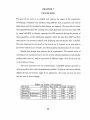
Table 4.1 TMS320C31 Characteristics
gives a software programmable gain, ranging from 1 to 1000, facilitating the handling
of signals with small amplitudes. The gain to be used is output to the latch along
with the channel number.
4.3 The TMS320C31 Digital Signal Processor
The TMS320C31 is a floating point, 32 bit DSP from Texas Instruments. Its key
specifications are listed in Table 4.1. The TMS320C31 has, besides the CPU, a
DMA controller, an instruction cache, RAM, ROM, Serial port, Timers, etc. all
integrated onto the chip. This translates into very high performance for the user. The
TMSC320C31 CPU consists of an ALU, a 32 bit barrel shifter, a 32 bit multiplier,
Auxiliary Register Arithmetic Units (ARAU s), and several registers in it. The
multiplier performs full 32 bit multiplications in just one cycle, and is capable of
operation in parallel with the other components of the CPU.The Arithmetic and
Logic Unit (ALU) performs single cycle operations on 32 bit integer, and 40 point
floating point data. The Auxiliary Register Arithmetic Units ARAU 0 and 1 generate
memory addresses in one cycle for the fast generation of memory addresses in the
various addressing modes.
The CPU also includes 28 registers in a multiport register file, tightly coupled
to the CPU. These are used to store operands right in the CPU so that they are
available for the instructions without any access delay. The on chip RAM blocks 0
and 1, are each 1K x 32 bits and the ROM is 4K x 32 bits. Each on chip memory
block can support two memory accesses in a single cycle. The instruction cache is 64
24
x 32 bits, i.e. 64 words large and maximizes the system throughput by caching the
repeatedly accessed code. The cache uses the Least Recently Used (LRU) strategy
for updating the cache memory from the main memory.
The TMS320C31 has a full duplex bi-directional serial port. The port can
transfer data in 1, 2, 3 or 4 bytes per word. The port can also be programmed in a
synchronous mode where continuous transfers can be done, transmitting many words
of data without new synchronization pulses. The TMS320C31 supports integer and
floating point data. Integer data types supported are 16 bit, 32bit, both signed and
unsigned. The floating point data types are short, single precision and extendedprecision. The use of floating point operations to manipulate data is of great
advantage, as the operation can be performed in a single cycle, while freeing the
user of the burden of implementing libraries to perform floating point operations.
The TMS320C31 has a 32 bit timer/counter that can be used for various
purposes. It can be driven off an internal clock, i.e. used as a timer, or an external
signal may be used to drive the timer, thus acting as a event counter. It can also
generate an interrupt to the CPU. The timer in the Dalanco Spry board is used
to trigger the conversions of the ADC. The TCLK pin is toggled to trigger the
conversion. The ADC performs the conversion and then sends the converted data to
the TMS320C31 serial port. Once the data is received the serial port may be read
to retrieve the data.
4.4 Initialization
The Dalanco Board needs initialization at startup. The ADC connects to the serial
port on the DSP. So the serial port and timer must be set up, and also the latch
on the Dalanco Spry Board must be set up. For this the InitDSP() function is
implemented. The function call prototype is
void InitDSP(void);
25
Table 4.2
Word Format for the ADC Latch
The function begins by setting up a few pointers. The latch in the Dalanco Spry
Board contains the ADC channel number and the gain for the programmable gain
amplifier (PGA). This latch is set up, as a default, to set the ADC channel to 0 and
a unity gain for the programmable gain amplifier. These are just the defaults, by
accessing the latch before each conversion the user can set the gain for the PGA as
well as set the channel. The function ReadAdc takes care of the function of setting
the channel.
The word format for the LATCH_VAL word is shown in Table 4.2. The bits
gi
and g0 set the gain of the programmable gain amplifier (PGA),while the bits m 1 and
m 0 set the channel for the ADC multiplexer. The PGA gain is set by the value of
the word g i g0 , i.e. 00 2 1 10 , 01 2 -4 10 10 , 10 2 100 10 and 11 2 1000 10 . The ADC
channel gets set to the value of the word m 1m0
, i.e. 00 2 Om, 012 -4
110, 1 02 -4
2i0
and 11 2 -4 3 1 0. The other bits in the LATCH_VAL are 'don't cares'. Following this
the function now sets up the DSP chip registers itself.
The registers set up are the Timer registers, and the Serial port control registers.
In the C31 these are memory mapped. To do this a pointer is set up to the register
area which in the C31 is at 808000 16 and the values are written to the registers.
This sets up the DSP to ADC communication on the serial port. The ReadAdc and
WriteDAC functions can now be called, to perform analog I/O as desired.
26
4.5 DAC Usage
The output to the analog channels is written via the DAC. The function call for this
is WriteDAC(..). The C prototype for this is:
int WriteDAC(int value, int channel);
This outputs the value to the DAC channel specified. Since the DAC has two
channels legal values for channel are 0 and 1. The value passed may be in the range
This clamping is done by the function WriteDAC and need not be performed
by the user. This is to avoid problems associated with 'roll over'. If the value is
greater than 2047, then it cannot be properly expressed in 12 bits and leads to
wrong interpretation of the value. Thus if a value of 4096 is output to the DAC with
an intended output value of 10V, it gets clamped to 5V only, since the DAC output
is restricted to 5V. Similar clamping occurs on the negative side.
The function WriteDAC retains the value output to the DAC channel 0 and
channel 1. For this reason the declaration for channel_value[] is prefixed with static.
The reason for maintaining the last value is that actually every time the DAC value is
updated, both the DAC values are to be written. In C, it is made to appear as if each
DAC is written to separately. While this is more convenient to use, it means that
the function WriteDAC must know the value of the other DAC previously written.
If this value is not stored, then when one DAC is written the other DAC output will
be trashed. Clearly this would be unacceptable, and this is overcome by storing the
previously output values. So actually the function WriteDAC always updates both
the DACs, and effectively makes it appear as if only one DAC is updated every time.
The value for the DAC channel 1 must be put into the upper 16 bits, i.e. right
justified in the upper 16 bit word. This shifting is done, and then the values for the
two channels are 'OR'ed together and then output via the serial port. Obviously if
27
both the converters are to be updated, then it is more efficient to do so in one call
and for this another function call, WriteDACS(..) is available. This function call
updates both the DAC channels in one call. The prototype for this function is:
int WriteDACS(int value°, int value1);
The channels 0 and 1 are updated with the values valuel and value2. This is
more efficient if both the converters are to be updated. For instance in our work,
the controller writes both the servo commands by calling this function, two calls to
WriteDAC are not used.
4.6 ADC Usage
To input analog values from the ADC the function ReadAdc() is called. The
prototype for this function is:
int ReadAdc(int channel);
This reads the value from the ADC for the voltage applied on the specified channel.
The function returns values ranging from —2048 to 2047 for voltages ranging from
—5V to 5V. The integer data type 'int' on the C31 DSP is 32 bits, while the
conversion result is 12 bits.
The necessary sign extension is performed internally and the user does not need
to perform any such extension. To read from more than one channel multiple calls
to ReadAdc are necessary.
Since the ADC on the card has four channels, legal values for channel are from
0 to 3. If the voltage at the ADC input is to be calculated then the ADC output
is simply multiplied by the scaling factor 5/2047. The function begins by writing
the channel (and the default gain of unity) to the latch. Once the latch is set the
function waits for the conversion to be triggered by the TCLKO pin toggling. This
pin is the output of the Timer 0.
28
Figure 4.2 Synchronization to TCLK
Whenever the count is complete the pin goes high, stays high for a clock period
and then goes low. This event is used for triggering the ADC in hardware. This also
is used to synchronize the software to a time source. The timer runs off the DSP
clock, in the timer mode, and its accuracy is determined by the DSP clock, which is
very good. This is the source of timing in all the control programs written with this
library.
4.7 Sampling Rate Determination
It is necessary to define the sampling rate for the system. This is done by defining
the constant TIMPERO. The functions WriteDAC and ReadAde both wait for the
falling edge of the TCLK signal in the C31 DSP. A sequence RWWRR synchronizes
up as shown in Figure 4.2.
This means that the sampling rate is determined by the value loaded into the
Timer 0 of the C31. Also since these functions wait for the falling edge, all the reads
and writes get synchronized to these falling edges. The Figure 4.2 shows an arbitrary
sequence of reads and writes as it would get executed. The function InitDSP puts
TIMPERO into the Timer 0 count register. The constant must be defined before the
file d310bio.h is included, so that the default value is not picked up. The value of
TIMPERO is calculated from:.
29
Figure 4.3 Successive Read and Write Events
where System, Clock = 50M H z. The factor numcalls is the total number of calls to
the functions ReadAdc and WriteDAC in one execution of the control loop. This is
to account for the fact that both functions wait for the falling edge of TCLK. So, for
example if TCLK has a frequency of 1kHz, and if the control loop has one ReadAdc
and one WriteDAC, then the loop will run 500 times per second.
The functions WriteDAC and WriteDACS must be distinguished with care, as
illustrated in Figure 4.3. The writes W1 and W2 are made using WriteDAC. The
writes W3 and W4 are mace with the function WriteDACS. Owing to the architecture
of the board, such paired writes may be made but paired reads are not possible. The
functions thus isolate the user from the unnecessary details of the board architecture
but reflect the restrictions that the architecture imposes on the operations to be
performed. The sampling rate may also be set dynamically as explained in the
following section.
4.8 Runtime Sampling Rate Determination
As explained in the previous section, the sampling rate is determined by the count in
the Timer 0 Period Register of the C31. This value is set up by InitDSP, but it can
also be altered within the program if the need arises. For this the memory mapped
Timer Period Register must be altered. This can be done very simply as follows:
int *period;
period=(int *)0x8008028;
*period=TIMER_PERIOD_DESIRED;
30
This changes the rate at which TCLKO pulses and sets the rate for the reads and
writes. Note that if this is to be done repeatedly, e.g. to generate a rectangular wave
(duty cycle not 50%) at the output of the DAC, then for good accuracy it would be
necessary to start and stop the timer while this is done and also to synchronize the
modifications with TCLK itself.
4.9 Data Exchange between the PC and the DSP Card
The data exchange between the DSP card and the host PC is accomplished by
calling the functions in the user library provided by the card manufacturer. For
more detailed information consult the users guide for the card.
CHAPTER 5
THE PLANT (PZT)
Piezoelectricity means "pressure electricity". Pierre and Jacques Curies discovered
it in the 1880's. It is the property of certain crystals , like Quartz, Rochell salt,
barium titanate, and many others, that when subjected to pressure these crystals
exhibit charges on their surfaces. The charges are proportional to the pressure and
appear only when pressure is present. Conversely when electric potential is applied
to these materials the dimensions of these crystals change. These materials are also
called smart materials.
These crystals are being considered as actuators in micropositioning applications and precision control systems.
5.1 PZT Ceramics Manufacturing Process
The manufacturing process of PZT starts with mixing and milling of raw materials.
The milled mixture is then heated to 75% of the sintering temperature. The polycrystallaine, calcinated powder is ball milled once again. Granulation with binder is
carried out to improve processing properties. After shaping and pressing the ceramics
is heated to 750° to burn out the binder.
The next phase is sintering at temperatures as high as 1250°C to 1350°C. The
ceramic block is then finished into the desired shape and tolerance. All processes
especially the sintering and heating need to be controlled to very tight tolerances.
The smallest change effects the properties and quality of the PZT. The direction
of polarization is established during the poling process by a strong electrical field
applied between two electrodes. For actuator applications the piezo properties along
the poling axis are most essential.
31
32
5.2 Advantages of Piezoelectric Positioning Systems
The advantages of piezoelectric positioning systems are:
• Unlimited Resolution:
A piezoelectric actuator (PZT) can produce extremely fine position changes
down to the subnanometer range. The smallest change in the operating voltages
are converted into smooth movements. Motion is not influenced by striction,
friction or threshold voltages.
• large Force Generation:
PZTs can generate forces in levels of 10,000 N.
• Fast Expansion:
PZT offers fastest response time, acceleration rates of more than 10,000 g's can
be obtained.
• No Magnetic Fields:
The PZT is related to electric fields and don't produce any magnetic fields or
interact with any magnetic field.
• Low Power Consumption:
The PZT consumes energy only during the motion, static operation even under
heavy loads does not consume power.
• No Wear And Tear:
PZT does not have any moving parts which will wear and tear and need
routine maintenance. It therefore can give satisfactory performance over a
long duration of time without any replacement.
• Vacuum and Clean Room Compatible:
PZT does not need to be lubricated and does not wear or abrase, thus is suitable
for vacuum and clean room applications.
33
• Operation at Cryogenic Temperatures:
The Piezo effect is based on electric fields and functions down to almost zero
Kelvin with reduced specifications.
5.3 Displacement of Piezo Actuators
Open loop Piezo actuators exhibit hysteresis like magnetic devices, this can be
eliminated by closing the loop. Hysteresis is based on crystalline polarization effects
and molecular friction. The absolute displacement generated by an open loop PZT
depends on the applied electric field and the piezo gain. Piezo gain is effected by
the electric field piezo, its deflection depends on its previous operating conditions.
Hysteresis is typically of the order of 10% to 15% of the command motion.
5.4 Considerations for PZT Usage
5.4.1 Mechanical Considerations
Every time the PZT drive voltage changes, the piezo element changes its dimensions
(if not blocked). Due to the inertia of the PZT mass (plus any additional mass),
a rapid change will generate a force acting on the PZT. The maximum force is
approximated as:
displacement without external force, and kT PZT actuator stiffness. Tensile forces
must be compensated to prevent damaging the PZT. Sinusoidal operation with
34
Figure 5.1 The Block diagram of our plant
and f the frequency in Hz.
5.4.2 Electrical Considerations
When operated far below resonant frequency PZT behaves like a capacitor where
displacement is proportional to the charge. PZT actuator stacks are assembled with
thin wafers of electroactive ceramic material electrically connected in parallel. A
measure of stack capacitance can be made by:
n is the number of layers, 6 0 dielectric constant in vacuum, e33 relative dielectric
.
constant, A= area of electrodes surface and d3 distance between electrodes.
Every change in the charge or displacement needs a current i:
35
Where i is current, U is voltage, C capacitance, and Q charge. For static
operation only leakage current has to be supplied. The high internal resistance
limits leakage current to low micro or submicro amp ranges.
5.4.3 Temperature Effects
Thermal stability of the PZT ceramics is better than most other materials. It is
characterized by the coefficient of thermal expansion. these coefficients are dependent
on the temperature.
PZTs work inside a range of temperatures. Even down to 0 degree Kelvin.
However, the magnitude of piezo gain is dependent on the temperature. Near room
temperature it is very stable.
5.5 Our Plant
The Block diagram in Figure 5.1 shows our plants components. Our plant consists of
a + like structure with 1 inch square in center and four squares one on each of four
sides. The target to measure the movement is mounted in the center of the structure.
The structure is mounted on a base such designed to allow multilayer stack of PZTs
also to make it easy to test them individually. We uses individual PZT's to gather
information about there performance and then made a four layer PZT plant to do
our PI control experiment.
The PZT is excited by using a 1:100 ratio DC amplifier to amplify the DSP
The displacement sensing of the PZT behaviour is carried out by using a
capacitive sensor. The gain of the capacitive sensor is 0.4. The capacitive sensor
is excited by a separate power supply of 5 volt DC and gives the deflection in the
36
of the capacitive sensor.
Delanco Spry 310 board. The board then transfers the data onwards to LabVIEW
for further processing.
CHAPTER 6
IMPLEMENTATION
6.1 The DSP Block
The DSP block of the is a VI which can be run at its own as well as connected to
other VIs as a subVl. It has an icon which allows it to be connected to three inputs
and give one output. The required inputs are:
• Sampling rate and integer input,
• Download / Execute selection a binary selector input,
• Input the data value that has to be written to the DSP, and
• Output the data returned to the LabVIEW by the DSP
When this is run at its own its front panel can be used to give and read the
status of the DSP what we are writing to D/A and what is being read back from
A/D.
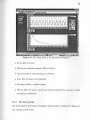
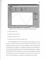
6.1.1 The Front Panel
The front panel of the DSP block is displayed in Figure 6.1 and consists of four
components:
• Control input for sampling rate,
• Control input for Data to be sent to DSP,
• Binary control button for operation during the run execution,
• The display for the data sent by DSP.
We can give integer values to the control input for the sampling rate, this value
is written to the CIN. The control for input Data sent to DSP accepts floating point
37
38
Figure 6.1 The Front Panel of the DSP Block
values for the data or the voltage level which is to be sent to the DSP tbe value is
in volts and has the precision of two decimal places, tbe display is also configured to
display only upto two decimal places. Tbe binary button select whetber we want to
download tbe DSP program to interface witb the DSP block VI into tbe DSP or we
want to execute tbe program in tbe DSP. This is done for convenience as well as better
utility of the system. The user is responsible to ensure that the proper interfacing
program is in the DSP before execut ing tbe DSP block. It is recommended that we
should always download once before we actually start tbe program. Tbe block is
configured to download tbe DSP program wben opened and tbe user bas to switcb
to execute mode before he can start using tbe DSP block VI. Tbe value read by tbe
DSP is also displayed as voltage witb two decimal point precision on the front panel.
Tbis VI can be run only once or can be put into repetitive runs from tbe control
toolbar on LabVIEW. Care sbould be taken in using tbe VI as a subVI since we will
39
need to DL the DSP program into the DSP. This VI is written so as to support and
provide capabilities for the user to develop his own experiments which use the DSP
to read and write one channel each.
6.1.2 The Block Diagram
The block diagram shows that the Sampling rate is written as it is to the CIN. the
Data to be sent to the DSP is however scaled as the DSP uses value 409 for outputing
1 volt through the D/A. This called value is provided to the CIN. The CIN can be
seen to have two I/O terminals and one output only terminal. The data sent by the
DSP is available at the output only terminal and is already properly scaled to give
the voltage read by the DSP. This whole logic is enclosed in a case true box and the
case value is decided by the download/execute button. Please refer to Appendix A
for the Figure A.1 which shows the case true block diagram.
Incase of the case false input from the download/execute button the block
diagram shown in the Figure A.2 in appendix A is executed. This calls the batch
file dsp.bat which compiles and downloads the DSP program to interface with the
LabVIEW DSP block VI.
6.1.3 The CIN
The CIN source code is available in the Appendix B. The CIN takes the sampling
rate and writes it down to the DSP memory address 0x01387. Then it writes down
the data to be sent to the DSP on address 0x1388. After doing that the CIN waits
for the DSP to actually send this data out to the D/A and read data from the A/D.
When the check flag is set the CIN reads the data value from the DSP address
0x01389 and ends its execution after resetting the check flag.
40
6.1.4 The DSP Program
The DSP program to interface with the DSP block VI is available in Appendix C.
The DSP program first checks if it is running the DSP at the desired sampling rate
then it manipulates and write the data at the address 0x01388 to the D/A. Then
reads and stores the data from A/D to the address 0x01389 and sets the check flag.
6.2 Hysteresis with Dither
Hysteresis is defined by Webster's Seventh new collegiate Dictionary as:
A retardation of the effect when the forces acting upon a body are changed
(as if for viscosity or internal friction); esp:a lagging in the values of
resulting magnetization in a magnetic material( as iron) due to a changing
magnetizing force. hys ter et ic adj
-
-
-
-
Hysteresis represent the history dependence of physical systems. If something
is moved and when released springs back to its original position, if it does not relocate
itself exactly on its original position it is exhibiting hysteresis. The term most
commonly associated with the magnetic materials. However, hysteresis occurs in
a lot of other systems, like bending of fork if pressed to hard etc.
Hysteresis loops happen when we repeatedly wiggle the system back and forth.
Some systems can be looped repeatedly and exhibit same or very slightly modified
hysteresis, others may not allow us to repeat the experiment. We can pulsate the
PZT as much as we like with care of not doing it too fast, but we cannot bend and
return the fork. Another important factor is the speed of the repetitions. if this is
done very quickly the system may not exhibit its true dynamics. If it is done too
slowly then the drifting of the system, as is the case with PZT, may play a role.
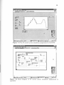
6.2.1 The Front Panel
The front panel of the DSP block is displayed in Figure 6.2 and consists of six
components:
41
Figure 6.2 The Front Panel of the Hysteresis program.
• Control input for sampling rate,
• Control input for Voltage level to be used during the experiment,
• Binary control button for operation during the run execution,
• The XY graph display for plotting the hysteresis loop,
• The data display for the DSP input,
• The data display for the DSP output.
We can give integer values to the control input for the sampling rate, this value
is written to the CIN. The control for Voltage level accepts floating point values for
the data or the voltage level which is to be sent to the DSP the value is in volts and
has the precision of two decimal places, the display is also configured to display only
upto two decimal places. The binary button select whether we want to download the
42
DSP program to interface with the DSP block VI into the DSP or we want to execute
the program in the DSP. The user is responsible to ensure that the proper interfacing
program is in the DSP before executing the Hysteresis VI. It is recommended that
program should always be download once before we actually start. The block is
configured to download the DSP program when opened and the user has to switch
to execute mode before he can start using the VI. Once the DSP has carried out the
experiment and had the data transferred to the LabVIEW, the data plotted or_
the XY graph and the user is a asked if data needs to be saved. The arrays of both
the DSP input and DSP output are also available in the displays for these purposes.
This VI can be run only once or can be put into repetitive runs from the control
toolbar on LabVIEW. This VI cannot be used as a subVI but only as an independent
VI. The execution time depends not only on the systems performance but also on
the sampling rate being used.
6.2.2 The Block Diagram
Once again the block diagram as shown in Figure A.3 consists of a true false case
selection controlled by the Download/Execute button. The true case block diagram
shows the sampling rate is directly transferred to the CIN, while the voltage is scaled
by a factor of 409.0 and then transferred to the CIN. The voltage has accuracy of
two decimal places as it is transferred to the CIN.
The CIN in this case writes back two arrays of data to the LabVIEW which
are stored in DSP input and DSP output arrays. These arrays are then combined
together to form a cluster of two dimensional data which is then passed on to the XY
graph. another two dimensional array is formed which is then passed on to subVl
write to spreadsheet. This subVl asks the user the name of the spreadsheet format
data storage field. This operation can be cancelled or completed by the user by a
file saving dialog box.
43
Incase of the case false input from the download/execute button the block
diagram shown in the Figure A.4 in appendix A is executed. This calls the batch
file hyst.bat which compiles and downloads the DSP program to interface with the
LabVIEW Hysteresis VI.
6.2.3 The CIN
The CIN creates two handles for the arrays of data which will be transferred between
the CIN and LabVIEW. It accepts two pointers one for sampling rate and another
for the desired maximum voltage level. An important thing to note is the NumericArrayResize function and its not so user friendly interface. Caution needs to
be exercised with this function since it causes LabVIEW to crash if not properly
handled. This function configures the data structure which will transfer data back
to LabVIEW.
The DSP is put into execution mode to perform the experiment. The CIN
calculates the hexadecimal value to be transferred to the DSP in order to get the
desired sampling rate as writes the result of these calculations to the DSP address
0x01387. The check flag is checked repeatedly until it is set by the DSP marking the
complete execution of the experiment. It is important to note that CIN allows non
LabVIEW programs to run in the Windows 95 environment.
Once the DSP confirms that the necessary data has been acquired, the CIN
reads the data input to the DSP from the address 0x01388 onwards and the DSP
output from address 0x02788 onwards. After necessary data scaling and manipulations the data is stored in the structures to be passed on to LabVIEW. The check
flag is rest to 0 and the DSP is halted to stop further execution of the program, as
CIN ends its execution.
44
It is important to note that the execution of this VI depends very heavily on
the sampling rate selected, and care needs to be exercised to select a sampling rate
which will not allow the dynamics of the system to be wrongly interpreted.
6.2.4 The DSP Program
The DSP program of the hysteresis experiment adjusts the sampling rate of the
system to the desired rate passed by the CIN. then it calculates the output signal
it needs to send out at that particular instant which depends on the position of the
position counter i. It is important to note that the program generates a triangular
waveform which goes from 0 to maximum then back through zero to minimum and
then again through 0 to maximum desired voltage level. The sampling rate has to
be slow enough to simulate DC voltage levels for the system rather than a triangular
waveform in practice a sampling rate of 50 samples per second was found to be a
good selection.
The DSP program writes the calculated value out in array starting from address
0x02788 and then copies the value from A/D converter to the array at address
0x01388 onwards. One the complete route for the hysteresis is completed the DSP
program sets the check counter thus informing the CIN that it has completed the
data acquisition for the desired experiment.
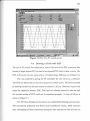
6.3 Range of PZT Displacement
6.3.1 The Front Panel
The range of the PZT plants displacement is measured by giving very low frequency
sine wave input to the DSP and reading the maximum and minimum voltage levels
and scaled to displacement. Therefore we have the following on the front panel:
• Control input for desired frequency of sine wave,
• Control input for sampling rate,
45
Figure 6.3 The Front Panel of the PZT Range
• Control input for Voltage level to be used during the experiment,
• Control input for bias level to be used during the experiment,
• Binary control button for operation during the run execution,
• The Waveform Chart to display the signal written by the DSP (Incoming
Signal) ,
• The Waveform Chart to display the signal coming back to the DSP (Outgoing
Signal),
• The Calculated range.
We can give frequencies with an accuracy of two decimal places, the fractional
Hz capability is necessary since the experiment needs to be carried out at the slowest
possible speed. The sampling rate has to be given in integer form . Voltage input
46
control is provided to accept voltage with accuracy of two decimal places. The binary
button can select whether we are going to Download the program into the DSP or
we are going to execute the program in the DSP.
It is important to note a few things here:
• The display of the data on the two waveform charts consumes a lot of resources
as well as time causing this particular VI to be excruciatingly slow.
• The display will become garbled and not easily understandable at relatively
higher frequencies.
• The fastest acceptable frequency cannot be ascertained as it depends heavily
on the applications running under windows, and the system hardware being
used.
• The higher sampling rate can cause the DSP and the display to get asynchronized
and the realtime effect can be lost.
Once the sine wave cycle has completed the PZT has passed through the
maximum and minimum levels of its displacement the range of PZT displacement
can be read from the display Range. Figure 6.3 shows the Front Panel.
This VI is a stand alone VI and cannot be connected to other VI's as a subVI.
It has to be run on the continuous run mode in the LabVIEW because we need to run
CIN each time we need new data and also necessary to keep the realtime operation
going.
6.3.2 The Block Diagram
The block diagram shown as Figure A.5, writes the sampling rate without any manipulation to the CIN, however the Frequency, Voltage and Bias levels are scaled by
a multiplying factor of 100 before being passed to the CIN. The CIN consists of
47
four integer input output terminals and three floating point output terminals. The
data coming from the CIN is already scaled and is displayed as it is on the charts
and in the range data display. This whole block is in a case true selection of the
download/execute button.
Incase of the case false input from the download/execute button the block
diagram shown in the Figure A.6 in appendix A is executed. This calls the batch
file range.bat which compiles and downloads the DSP program to interface with the
LabVIEW Range VI.
6.3.3 The CIN
The CIN puts the DSP in execute mode and then writes the desired frequency,
sampling rate, voltage and bias level to the DSP. then when the DSP gives the check
flag the new values for both input and output charts are read and the range as
determined by our algorithm in the DSP is also read after which the check flag is
reset. It is imperative to notice once again that this experiment is supposed to run
at slower speeds.
The
6.3.4
The DSP Program
DSP program accepts the sampling rate at address 0x0:387, frequency at address
0x0138b, bias at address 0x0138c, voltage at address 0x0138d, and gives the range at
address 0x0138a, input to the plant at address 0x01388, and output from the plant
at address 0x01389.
The desired sampling rate is set, and from this sampling rate information the
sampling time T, is calculated. The 0 is then calculated as follows:
This theta is then used to calculate the sine waveform, and the sine wave is
multiplied with the desired voltage and the bias is added before it is sent out to the
48
plant. The number n is incremented each time until the 0 reaches a value of 2 r then
n is reset since:
The range is calculated as the difference between maximum and the minimum
voltage sensed by the PZT displacement sensor scaled and then written to the
address.
6.4 Resonant Frequency Determination
The conditions of dynamic stability instability are commonly expressed in mechanics
of vibrations in terms of frequency relationships and the related mechanical
phenomenon is called resonance. Systems with constant coefficients in their DE's
have most generally the frequency relationship of form:
where v is the excitation frequency, wj is one of the natural frequencies, and p
and q are usually small relatively prime numbers. The motion of the system in the
vicinity of v are resonance oscillations, with amplitude aj of one mode corresponding
to the natural frequency wj. The frequency v is called the critical frequency.
For the systems whose governing DEs of motions have periodic coefficients, the
frequency relationships are of the following form:
positive integer and k r are integer.
Practical steps in solving the problems of resonance oscillations are :
49
Figure 6.4 The Front Panel of the Resonance Frequency
• Set up DEs of motion
• Obtain and normalize temporal DEs of motion
• Apply asymptotic representations of solutions
• Solve DEs for phase and amplitudes
• Determine stable / unstable regions
• Discuss effects of various system and external excitation on resonance modes
of resonance oscillations
6.4.1
The Front Panel
The front panel of the resonance frequency determination is displayed in Figure 6.4
and consists of four items:
50
• Control input for sampling rate,
• Binary control button for operation during the run execution,
• The graph displaying the data gathered in time domain
• The display data gathered in the frequency domain
We can give integer values to the control input for the sampling rate, this value
is written to the CIN. The binary button select whether we want to download the
DSP program to interface with the DSP block VI into the DSP or we want to execute
the program in the DSP. It is recommended that we should always download once
before we actually start the program. The block is configured to download the DSP
program when opened and the user has to switch to execute mode before he can
start using the DSP block VI.
This VI can be run only once or can be put into repetitive runs from the control
toolbar on LabVIEW. The modes of frequency display are prominent high amplitude
peaks which stand out in the frequency domain display. Single sided FFT is carried
out and the results are plotted for a sampling of 8192 data points.
6.4.2 The Block Diagram
The block diagram shows that the Sampling rate is written as it is to the CIN.
The CIN has one output only terminal. The data sent by the DSP is available at
the output only terminal and is already properly scaled to give the voltage read by
the DSP. This data is collected by LabVIEW in the form of an array and then the
FFT operation is performed, as well as this data is displayed in the time domain
data display screen. The array size is determined, and then the single sided data
for frequency domain display is extracted. Then this data, which is in real and
imaginary parts, is processed for amplitude and phase calculation by the complex to
polar VI. The resulting data is divided by 2 if nonzero and then a cluster is formed
51
which is given to the frequency domain display graph. Figures A.7, A.9 show the
Block diagrams .
Incase of the case false input from the download/execute button the block
diagram shown in the Figure A.8 in appendix A is executed. This calls the batch
file range.bat which compiles and downloads the DSP program to interface with the
LabVIEW DSP block VI.
6.4.3 The CIN
The CIN puts the DSP in execute mode and then writes the desired sampling rate
to the DSP. When the DSP gives the check flag the values for input are read and
the check flag is reset. Finally the DSP is halted before the CIN is finished.
6.4.4 The DSP Program
The DSP checks and keeps the sampling rate to the desired sampling rate as given
by the CIN. Then it collects data from the input and once all required data is
accumulated the DSP sets the check flag.
6.5 PI Control Application
PID controllers are the most widely used practical controllers. The "textbook"
version can be described by equation:
where e is the error, difference between command signals u, (the setpoint) and
process measured output y. K is the gain or proportional gain of the controller. Ti
the integration / reset time. and Td the derivative time. A pure derivative cannot be
implemented, because it will give a very large amplification of measurement noise.
With this perception only a PI controller was implemented in our case.
52
The controller can be discretized using any of the standard methods such
as Tustin's approximation or ramp equivalance. Tutsin's approximation gives a
given as :
It has the advantage that all three terms can be calculated separately.
The incremental algorithm is obtained by rewriting the control algorithm such
that its output is the increment of the control signal. Au can be calculated as:
we use this to get:
This is called the incremental form of the controller. A drawback of incremental
controller is that it cannot be used for P or PD controllers.
6.5.1 The Front Panel
The front panel of the PI control VI is displayed in Figure 6.5 and consists of
following:
• Control input for sampling rate
• Control input for reference (setpoint)
• Control input for the Proportional gain KP
• Control input for the integral gain KI
• Binary control button for the download / execution selection
53
Figure 6.5 The Front Panel of the Proportional Integral program.
• Control input for bias
• Display for the value of y(n)
• Display for the value of urn)
• Graph of the data received by the DSP, (y( n))
We can give integer values to the control input for the sampling rate, this value
is written to the CIN. The control for inputs for KI, KP, bias and reference accept
floating point values for the data to be sent to the DSP, the value has the precision of
two decimal places, the display is also configured to display only two decimal places.
The binary button select whether we want to download the DS!, program to interface
with the DSP block VI into the DSP or we want to execute the program in the DSP.
The data which is most current is displayed as the y(n) and urn) on the screen as
well as the u(n)is plotted so as to facilitate in the tuning of the PI controller.
54
This VI can be run only be put into repetitive runs from the control toolbar
on LabVIEW. Care should be taken in using the VI as a subVl since we will need to
DL the DSP program into the DSP. This VI is written so as to support and provide
capabilities for the user to develop his own experiments which use the DSP to read
and write one channel each and perform a PI control.
6.5.2 The Block Diagram
The block diagram shows that the Sampling rate is written as it is to the CIN. The
CIN has six Input/Output terminals accepting the Reference, KI, KP, Bias and the
iteration number i. All data except the sampling rate and the iteration number are
scaled by a factor of 100 to give two decimal places accuracy. It has two outputs one
for y(n) other for u(n). The data sent by the DSP is available at the output only
terminal and is already properly scaled to give the voltage read by the DSP. y(n)
data is only displayed in the digital format to give a form of feedback as to the output
DSP is giving and the u(n) is not only displayed but also plotted to display the actual
performance of the PI controller. The Block diagram is shown in Figure A.10.
Incase of the case false input from the download/execute button the block
diagram shown in the Figure A.11 in appendix A is executed. This calls the batch
file pi.bat which compiles and downloads the DSP program to interface with the
LabVIEW PI control VI.
6.5.3 The CIN
The CIN accepts the data from the LabVIEW and passes it to the DSP then it waits
for the DSP to signal via check flag that it has actually carried out one sampling of
I/O data. Then the y(n) and u(n) are read from the DSP and transferred back to
LabVIEW and the check flag is reset for another operation to be repeated.
55
6.5.4 The DSP Program
The DSP program accepts bias at address 0x0138a, sampling time at address
0x01387, check flag at address 0x01386, u(n) is handled at address 0x01388, and
y(n) is handled at address 0x01389, KP at address 0x0138b, KI at address 0x0138c
and the reference at address 0x0138d.The sampling time T is calculated. The error
e(n) is calculated as difference between the reference and the feedback from plant.
KP and Ki are scaled, and then the output for the plant is calculated as:
then y(n) is scaled to stay within bounded limits, and the values of y(n) and
e(n) are recorded as y(n-1) and e(n-1) for the next sampling. Finally the check flag
is set to inform the CIN that the DSP has completed the task assigned.
CHAPTER 7
CONCLUSION
The goal of our work is to simplify and improve the speed of the experiment.
Developing a Graphical user interface using DSP for data acquisition and control
applications and the interface for data display and analysis. We were able to reduce
the experiment duration for carrying out a simple hysteresis curve by more than 70%
by using LabVIEW to directly supervise the DSP operation during the process of
data acquisition, set the experiment setpoints, collect the data from DSP and then
carrying out the necessary analysis and displaying and storing the data if desired.
This also improved the end result in the form of our X-Y graph, as we were able to
get better resolution and overall a smoother graphical representation of our results.
Similar time savings were achieved for all experiments. The normal course of
carrying out an experiment was to use two or more software platforms to individually
perform each and every task of experiment at different stages. Now all the user has
to do is press a button.
The most important issue was of performance. LabVIEW software provides us
with an excellent tool called the performance profiler. It gives an interactive tabular
display of time and memory usage of our application. Our main concern was time
and the rate of data exchange.
Table 7.1 Profiles of VI programs
56
57
Figure 7.1 The Block diagram of data flow
The Table 7 shows profile of test results of running the VI's for 10 times.
Important thing to remember is that the Range of displacement and the PI are real
time VI's and therefore their exact number of execution may have varied.
We were able to achieve an average data exchange rate of 15 K during experiments which did not require the data to be displayed on the screen until all analysis
was completely carried out. The displaying, specially of the graphs and charts is a
very time consuming process and thus the real time display applications like Range
measurement and PI control have significantly slower data exchange rates. However,
the exact data exchange rate cannot be ascertained for these applications since it
varies very drastically as Windows 95 allocates time of execution for each program.
The data flow in our systems is shown as a block diagram in Figure 7.1. All
lines indicate the bidirectional flow of data. Each exchange of data is carried out in
a certain amount of time. The data on the Front panel is transferred to the memory
58
Figure 7.2 Dithering in the X-axis of Plant
location of the data in Block diagram, then block diagrams data is exchanged with
CIN in the form of pointers and handles, and the data exchange between the DSP
and CIN is actual I/O just like it is in case of the DSP and the plant.
7.1 Dithering
It is well known that the PZT voltage-displacement response exhibits hysteresis type
of nonlinearity. This hysteresis loop has more of a ovular shape than the classical
hysteresis shape.
A dither is a high frequency signal introduced into a nonlinear system in order
to linearize its performance. By sweeping back and forth quickly across domain of a
59
Figure 7.3 Dithering in the Y-axis of Plant
nonlinear element, a dither sort of averages the nonlinearity. This averaging action
can reduce the nonlinearity in the system.
We calculated the dither by selecting the frequency of the most prominent
resonance mode, and dividing it by the bandwidth required for a 3 dB drop. This
gave us the Q factor. Then depending on this Q factor we calculated the approximate
voltage to introduce different magnitude dithers into our system. We used dithering
for 1µm (small), 5 µm(medium), and 10µm(large) dithering signal.
Dither has the effect of attenuating the harmonic components of the fundamental waveform applied to it. The effects of the dithering on the harmonics were
checked using the VI for Resonant Frequency response. A sine wave of 1 volt
amplitude was applied and the harmonics introduced by the nonlinearity of the
PZT were attenuated using the dithering. One of the results of dithering is shown
in Figure 6.4.
60
Table 7.2 Effects of Dithering on Harmonics
These results in Table 7.1 point to the fact that we need a bigger dithering
amplitude to completely attenuate the harmonics, on the other hand bigger dithering
also causes a lot of additional oscillations to be introduced into the system. The ideal
amplitude of the dither cannot be ascertained.
7.2 PI Completely Programmed in LabVIEW
A complete PI control algorithm was implemented in the LabVIEW using the DSP
Block VI as a subVI to implement a single loop PI control. The maximum operating
frequency was 1000 samples per second, the PI algorithm was developed with a
built in one sample delay. The DSP Block gave us the values of the Un and Yn
which were stored in the shift registers. Thus using the yn-1, yn-2, en-1 and en2 to implement the discretized PI control completely in the LabVIEW. The Block
diagram is available in Figure 7.5
The usual Sampling rate, Operation contrl, KI, KP, Yn, Un and a chart
diplaying the current status were implemente din the front panel as in Figure 7.4.
61
fie E<i
~ete fmject ~Indowf
-""'"
ll!iOO
~filll
•••
I
2.
!\!J
~h .1Il
!>!'I
iii..
......
~
I
I
fll1l
....
p::;j
3.•
:n;
f2" I
l!O
::J1.:g:::Jl;o;3reG
5.•
I
~
(
t!
~3pt~aiIOnFont
¢-
I
1.•
0.•
-1.0
·2.
·1.
)
; 1
,
6S1
_ _ ' ,i
1115,.,1 ~HPSt""Wndow I LIbVIEW
II~PI control ........ mPicorhol.,fntmo. .. 1*SMglt132
I !. 3:53PM
Figure 7.4 The PI control system completely programmed in LabVIEW
m
"SIMI ~HPSt4M\lfni:lw IlAtNIE\oI
I E2P1 txnrol.,r.. rno.•. II~PI control in lin ... .,Srwi9V32
I I. 151 PM
Figure 7.5 Block Diagram of PI control system completely programmed
LabVIEW
111
62
Figure 7.6 The Two PI control system
.7-:3
Drawing a Circle with PZT
The use of PI control was enhanced to control two axis of the PZT structure, also
instead of single layered PZT we used a four layered PZT stack to draw a circle. The
PZT is driven by two sine waves with a 7r /2 radian phase difference as in Figure 7.6.
This was achieved by giving the PI controllers the sine waves as a reference.
The PZT was driven thus to move in a manner as to draw circles. We were successful
in drawing circles from 25 nano meters to almost 11.25 /lm. However, beyond this
range the capacitive sensors, ADC, DAC and our software started to saturate and
the circular motion of PZT could not be monitored properly. A circle of 3.0 /lm is
shown in Figure 7.7
The GUI was developed to be easy to use, aesthetically pleasing, and accurate.
The experiments performed were found to give satisfactory results. With extensive
data exchanging and data conversions during the data transactions and also the use
63
Figure 7.7 The output from PZT as a circle
of 12 bit capability of the DAC/ ADC we were able to perform operations with 95%
accuracy in the worst case scenarios.
The future of the work can span more experiments to be incorporated in the
system. The improvement of the graphic display experiments, developing and implementing the experiments using the DSP Block which do not need any code to be
written in the DSP. Incorporating other control algorithms. Studying and further
improving the dithering technique for the PZT. Improving the performance of the
interface to higher frequencies of data exchange.
APPENDIX A
THE BLOCK DIAGRAMS
64
65
I
l
.•.
---~
[)~~ sent by DSPI
I
I'~
Figure A .1 The Block diagram of the case t rue DSP Block
, .. . .
..
flo .f" llla'" Eo"",,
~~IQI
'-,
!,
!
L,
-
~~
113p4 AppIic~1OfI font
~ x
,;;]
~ I:c~ I.,.~ i<lG
.:. .
~
------~
I
I'"
~
1'"1: !J/
fl
Cormwld com Ie ds
_ b~
~I
•
o::m
-I
.
-',l--------~ -
Figure A .2 The Block diagram of the case fal se DSP Block
I
~'".,-
-
I"::;!
--.
66
I
¢
_
. • ;
~
x
ell
T~
...
Figure A.3 The Block diagram of the case true Hysteresis
r-- .
~-j
I cOlT'fMrld,com Ie
hyst.bal:t-----B
,.~
W!I
Figure A.4 The Block diagram of the case fal se Hysteres is
67
I
_
.•.
~
x
T~
~ --;
l
ga
m
I
.r;!
Figure A.5 The Block diagram of the case true range of di splacement
,...
Icomtl'\al'ld com Ie range botl
B
I.
TOJ""
Figure A.6 The Block diagram of the case false range of di splacement
68
Figure A.7 Th e Block di agram of t he case true Resonance Frequency
1 .1.
_ "
x
. 0.
Figure A.8 The Block di agram of the case false Resonance Frequency
69
_
x
~
RF
OSP
I
.r.J
Figure A.9 The Second Block diagram of the case true Resonance Frequency
_
~
x
;;;------------------------I~p
:~fllcOill:o:;:~rreG
Figure A.tO The Block diagram of the case true Proportional Integral Control
70
Figure A.ll The Block diagram of the case false Proportional Integral Control
APPENDIX B
THE CINS
B.1 The DSP Block CIN
/*
CIN source file the DSP block. The DSP is set to go
then the Sampling time and the desired signal are
written to the DSP, DSP then writes out this value
to the outside world reads a value which is then
wrote back to LAbView.
*/
/* ENTER YOUR CODE HERE */
// All variables used in this function are declared.
//
// Start the DSP program execution.
//
inp(0x306);
while (check != 1)
{
71
72
73
74
B.2 The Hysteresis CIN
/*CIN source file for the hysteresis measurement. The
DSP is set to go then the Sampling time and the desired
voltage range are selected and PC waits for the DSP to
finish and then loads all data into the LabView arrays.
*/
#include ''extcode.h"
#include<stdio.h>
#include<math.h>
#include<conio.h>
/*
* typedef s
*/
typedef struct {
int32 dimSize;
float64 arg1[1];
} TD1;
typedef TD1 **TD1Hd1;
CIN MgErr CINRun(int32 *Sampling_Rate, TD1Hd1 DSP_Input,
TD1Hd1 DSP_Output, int32 *voltage);
CIN MgErr CINRun(int32 *Sampling_Rate, TD1Hd1 DSP_Input,
TD1Hd1 DSP_Output, int32 *voltage) {
/* ENTER YOUR CODE HERE */
// All variables used in this function are declared.
//
75
76
77
78
B.3 The Displacement Measurement CIN
/*
CIN source file for the PZT movement range measurement.
The DSP is set to go then the Sampling time and the
desired signal are written to the DSP, the DSP then
writes out this value to the outside world reads a value
which is displayed on the chart, it also calculates and
transfers the range of the readings.
79
80
81
82
B.4 The Resonance Frequency Calculation CIN
/*
CIN source file for the resonant frequency measurement.
The DSP is set to go then the Sampling time is selected
and PC waits for the DSP to finish and then loads all
data into the LabView arrays.
83
84
85
B.5 The PI Control CIN
CIN source file for PI control. The DSP is set to go
then the Sampling time, reference, KI, KP, and Bias
are wriiten to the DSP, the DSP then writes out this
value to the outside world reads a value which is
displayed on the chart, it also calculates controls
the plant with PI algorithm.
86
87
88
APPENDIX C
THE DSP PROGRAMS
C.1 DSP Program for the DSP Block Program
89
90
C.2 The Hysteresis Program
91
92
C.3 The Displacement Calculation Program
93
94
C.4 The Program for Resonance Frequency
95
C.5 The Proportional Integral Control Program
96
97
REFERENCES
1. Texas instruments TMS320C31 Addendum to the TMS320C3x User's Guide,
1990.
2. Texas instruments, TMS320C3x User's Guide, 1990.
3. Texas instruments TMS320 Floating-point DSP optimizing C Compiler, 1995.
4. Dalanco Spry, 89 Westland Ave, Rochester, NY. TMS320 Floating-point DSP
optimizing C Compiler, 1995.
5. Geoff Lee. Object Oriented GUI Application Development. Prentice Hall
Englewood Cliffs, NJ 1993.
6. Mark A. Krasnoselski, Aleksei V. Pokrovski. Systems with Hysteresis, SpringerVerlag, NY 1989.
7. Karl J. Astrom, Bjorn Wittenmark. Computer Controlled Systems Theory And
Design, Prentice Hall, Upper Saddle River, NJ 1997
8. Tian Hong Control of Smart Structure using adaptive dither Masters Thesis
Department of Electrical and Computer Engineering New Jersey Institute
of Technology, Newark, NJ , 1994
9. http://www.lassp.cornell.edu/sethna/hyteresis/WhatIsHysteresis.html What is
Hysteresis., 12/22/98.
10. National Instruments Lab VIEW User Manual, Jan 1998.
11. National Instruments G programming Reference Manual, Jan 1998.
12. National Instruments Lab VIEW Function and VI Reference Manual, Jan 1998.
13. R.M. Evan-Iwanowski. In R. Cooper, editor, Resonance Oscillations in
Mechanical Systems, Elsevier Scientific publishing company, New York,
1976.
98