1
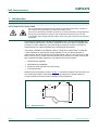
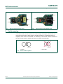
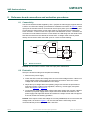
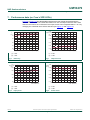
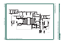
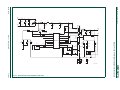
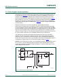
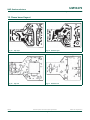
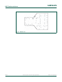
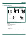
UM10479 SSL2101 120 V 7.5 W GU10 flyback reference board Rev. 1.1 — 19 August 2011 User manual Document information Info Content Keywords SSL2101, flyback, convertor, dimmable, active bypass Abstract This document explains the operation and application of a 7.5 W 120 V dimmable LED driver featuring SSL2101. The demo board has a form factor that is compatible with the base of a GU10 LED lamp. UM10479 NXP Semiconductors SSL2101 120 V 7.5 W GU10 flyback reference board Revision history Rev Date Description v.1.1 20110819 second version Modifications: v.1 UM10479 User manual 20110707 • • Table 1 “Specification” on page 5: values changed. Section 7 “Performance data (on Cree’s XPE LEDs)” on page 8: first paragraph added to. first version All information provided in this document is subject to legal disclaimers. Rev. 1.1 — 19 August 2011 © NXP B.V. 2011. All rights reserved. 2 of 23 UM10479 NXP Semiconductors SSL2101 120 V 7.5 W GU10 flyback reference board 1. Introduction WARNING Lethal voltage and fire ignition hazard The non-insulated high voltages that are present when operating this product, constitute a risk of electric shock, personal injury, death and/or ignition of fire. This product is intended for evaluation purposes only. It shall be operated in a designated test area by personnel qualified according to local requirements and labor laws to work with non-insulated mains voltages and high-voltage circuits. This product shall never be operated unattended. This document explains the operation and application of a 7.5 W 120 V dimmable LED driver featuring the SSL2101. The demo board has a form factor that is compatible with the base of a GU10 LED lamp. The board employs a flyback converter to provide an isolated solution for mains-dimmable LED recessed-light applications. The board is available in two different versions, designed to support both a 5-LED and 7-LEDs load with an output power of approximately 7.5 W. The board operates at approximately 45 kHz and produces a regulated output current of 470 mA for the 5-LED load or 340 mA for the 7-LED load, with an efficiency of around 73 %. Both versions are fully compliant with EMC regulations. Key features of the board include: • • • • Deep dimming capability Wide dimming compatibility Small form factor tailored to fit a GU10 lamp Cost effectiveness Dimensions of the board are shown in Figure 1. The board is shaped to fit in the base of a GU10 LED lamp. Board components are precisely placed on the board to allow for enough headroom when the board is inserted into the lamp base. 20.6 mm 18 mm 18 mm 34.1 mm 9. 2 m m Fig 1. UM10479 User manual 019aac434 Board dimensions All information provided in this document is subject to legal disclaimers. Rev. 1.1 — 19 August 2011 © NXP B.V. 2011. All rights reserved. 3 of 23 UM10479 NXP Semiconductors SSL2101 120 V 7.5 W GU10 flyback reference board 019aac460 Fig 2. SSL2101 demo board (top view) 019aac461 Fig 3. SSL2101 demo board (bottom view) 2. Safety warning The board needs to be connected to the mains voltage. Touching the board while it is connected to the mains voltage must be avoided at all times. An isolated housing is obligatory when used in uncontrolled, non laboratory environments. Galvanic isolation of the mains phase using a variable transformer is always recommended. 019aab174 019aab173 a. Isolated Fig 4. UM10479 User manual b. Not isolated Variac isolation symbols All information provided in this document is subject to legal disclaimers. Rev. 1.1 — 19 August 2011 © NXP B.V. 2011. All rights reserved. 4 of 23 UM10479 NXP Semiconductors SSL2101 120 V 7.5 W GU10 flyback reference board 3. Specification 3.1 Demo board performance and specification Table 1. Specification Parameter Value Comment AC line input voltage 108 V (AC) to 132 V (AC) Nominal input 120 V, 60 Hz Output voltage 16 V 5-LED string load 22 V 7-LED string load 455 mA 5-LEDs; 3.5 % 330 mA 7-LEDs; 3.5 % Output current Efficiency 73 % Power factor 0.93 5-LEDs 0.945 7-LEDs Output current ripple 30 % 5-LEDs 22 % 7-LEDs Switching frequency 45 kHz Output current regulation 5 % 10 % offset nominal line voltage 4. Functional description The LED driver uses the SSL2101 control IC. The SSL2101 is a Switched Mode Power Supply (SMPS) controller with an integrated MOSFET. Detailed information about the operation of SSL2101 can be found in its data sheet, see Ref. 1. The driver employs flyback converter topology with secondary current regulation. The converter operates in Discontinuous Conduction Mode (DCM), or a Boundary Conduction Mode (BCM), with valley switching detection. In BCM, valley switching detection is used to minimize magnetic component and switching losses while enhancing efficiency. The demo board is triac dimmable. When dimmers are used, the circuit detects the rectified voltage change and reduces the switching duty cycle to reduce the output current. The SSL2101's own internal strong and weak bleeders are used to supplement the current in the circuit to provide for the hold and latch currents required by triac dimmers. The circuit is compatible with a broad range of dimmers as shown in Table 2 UM10479 User manual All information provided in this document is subject to legal disclaimers. Rev. 1.1 — 19 August 2011 © NXP B.V. 2011. All rights reserved. 5 of 23 UM10479 NXP Semiconductors SSL2101 120 V 7.5 W GU10 flyback reference board 5. Dimmer compatibility Several dimmers have been tested as different dimmers have different specifications, the dimming performance of the board may vary. Table 2 shows the range of mains dimmers tested for compatibility with the SSL2101 demo board. Table 2. UM10479 User manual Dimmer compatibility Manufacturer Model number Voltage/type Compatibility LUTRON S-600 120 V/incandescent Yes LUTRON S-600P 120 V/incandescent Yes LUTRON S600-H 120 V/incandescent Yes LUTRON TG-600PH 120 V/incandescent Yes LUTRON DVW-600PH 120 V/incandescent Yes LUTRON DVW-603GH 120 V/incandescent Yes LUTRON DVM-600PH 120 V/incandescent Yes LUTRON DV-603PG 120 V/incandescent Yes LUTRON DV-600P 120 V/incandescent Yes LUTRON DV Beta Build 120 V/incandescent Yes LUTRON CTCL-153PDH 120 V/incandescent Yes LUTRON GL-600PH 120 V/incandescent Yes LUTRON Credenza S31 120 V/incandescent (lamp) Yes LEVITON 6631 120 V/incandescent Yes LEVITON 6602 120 V/incandescent Yes LEVITON 6602-I 120 V/incandescent Yes LEVITON RPI06 120 V/incandescent Yes Unknown GL410A 120 V/incandescent (lamp) Yes GE 18021 120 V/incandescent flicker GE 52136 120 V/incandescent flicker All information provided in this document is subject to legal disclaimers. Rev. 1.1 — 19 August 2011 © NXP B.V. 2011. All rights reserved. 6 of 23 UM10479 NXP Semiconductors SSL2101 120 V 7.5 W GU10 flyback reference board 6. Reference board connections and evaluation procedures 6.1 Connectivity The GU10 LED driver board supplied by 120 V (AC) 60 Hz mains supply supports either a 5-LED or a 7-LED load. Setting up the board for evaluation is as shown in Figure 5, where input pins W1 and W2 must be connected to the AC input power (Line and Neutral), and an LED string in series with a current meter must be connected to the two output pins LED+ and LED. Current comes out of pin LED+ and flows back to LED. Therefore, the connection must be made so that the current enters the LED string from the anode of the first LED and exits from the cathode of the last LED. A voltage meter must be placed directly across the two LED+ and LED pins for a more accurate reading. line current meter W1 LED+ neutral A W2 V voltage meter LED string LED- 019aac452 Fig 5. Board connections Remark: All connections must be made with input power switched-off. 6.2 Evaluation Set-up the board for testing and complete the following: 1. Switch-on the power supply 2. Check the LED current and voltage from the current and voltage meters. If there is no output, switch-off the power supply and check all connections. Once the correct voltage and current are established move to step 3. 3. Adjust the input voltage within the operating range. Now monitor the performance matrixes including, output current regulation, efficiency, current ripple, and power factor. See Figure 6 to Figure 10. 4. To test dimmer compatibility, switch-off the input power supply then connect a dimmer between input power supply and the input of the driver board. Now switch-on the power supply and adjust the dimmer and monitor the output current and LED light for a smooth, flicker-free dimming operation. Remark: If the output current and voltage are correctly established, the current meter and voltage meter, as shown in Figure 5, can be removed and the LED string can be connected directly to the output pins LED+ and LED. UM10479 User manual All information provided in this document is subject to legal disclaimers. Rev. 1.1 — 19 August 2011 © NXP B.V. 2011. All rights reserved. 7 of 23 UM10479 NXP Semiconductors SSL2101 120 V 7.5 W GU10 flyback reference board 7. Performance data (on Cree’s XPE LEDs) Figure 6 to Figure 10 provided detailed performance test results associated with the SSL2101 demo board. The results are based on a 470 mA output current for the 5-LED load and 340 mA for the 7-LED load. The output current can be adjusted within 10 % by changing the combined value of R21 and R23 (see Figure 11 and Figure 12). 019aac462 75 η (%) 70 (1) (2) (1) 65 0.45 60 0.40 55 0.35 50 108 114 120 126 132 input voltage (V) (2) 0.30 108 (1) 5-LED (1) 5-LED (2) 7-LED (2) 7-LED Fig 6. Efficiency Fig 7. 019aac464 11.5 input power (W) 11.0 (1) 10.5 (2) Output current 019aac465 (1) 0.80 126 132 input voltage (V) 0.75 108 (1) 5-LED (1) 5-LED (2) 7-LED (2) 7-LED Fig 8. Input power UM10479 User manual 126 132 input voltage (V) 0.90 9.5 120 120 (2) 0.85 114 114 1.00 power factor 0.95 10.0 9.0 108 019aac463 0.55 output current (A) 0.50 Fig 9. 114 120 126 132 input voltage (V) Power factor All information provided in this document is subject to legal disclaimers. Rev. 1.1 — 19 August 2011 © NXP B.V. 2011. All rights reserved. 8 of 23 UM10479 NXP Semiconductors SSL2101 120 V 7.5 W GU10 flyback reference board 019aac466 40 ripple (%) 35 (1) 30 25 (2) 20 15 108 114 120 126 132 input voltage (V) (1) 5-LED (2) 7-LED Fig 10. Output current ripple 8. EMI Both versions of the SSL2101 demo board are fully pre-compliant to EMC regulations. UM10479 User manual All information provided in this document is subject to legal disclaimers. Rev. 1.1 — 19 August 2011 © NXP B.V. 2011. All rights reserved. 9 of 23 xxxx xxxxxxxxxxxxxxxxxxxxxxxxxxxxxx x xxxxxxxxxxxxxx xxxxxxxxxx xxx xxxxxx xxxxxxxxxxxxxxxxxxxxxxx xxxxxxxxxxxxxxxxxxxxxx xxxxx xxxxxx xx xxxxxxxxxxxxxxxxxxxxxxxxxxxxx xxxxxxxxxxxxxxxxxxxxxx xxxxxxxxxxx xxxxxxx xxxxxxxxxxxxxxxxxxx xxxxxxxxxxxxxxxx xxxxxxxxxxxxxx xxxxxx xx xxxxxxxxxxxxxxxxxxxxxxxxxxxxxxxx xxxxxxxxxxxxxxxxxxxxxxxx xxxxxxx xxxxxxxxxxxxxxxxxxxxxxxxxxxxxxxxxxxxxxxxxxxxxx xxxxxxxxxxx xxxxx x x MOV1 C10 0.1 μF 250 V C2 47 nF 250 V BD1 R9 3.9 kΩ R2 D1 L1 680 μH US1G-13-F MB2S C1 0.1 μF 630 V RGND C4 0.1 μF 630 V C3 100 pF C13 0.22 μF 630 V isolation 68 Ω Q2 MPSA92 R7 R6 2.4 kΩ R3 2.7 kΩ R4 4.7 kΩ R5 110 kΩ VCC C7 10 μF 16 V T1 7 1 6 2 R25 330 Ω SBLEED DRAIN WBLEED GND VCC GND GND GND BRIGHTNESS R11 R10 470 kΩ 16.2 kΩ 10 U1 GND C8 8 D5 pri RGND R8 14.3 kΩ D2 US1G-13-F RC2 RC SSL2101 aux 9 3A 100 V 4 sec C5 1000 μF 25 V C11 1000 μF 25 V R19 5 LED- 0.3 Ω C12 22 nF 2 kV GND 2 R12 SOURCE R13 33 kΩ 0.68 Ω AUX ISENSE R14 10 Ω R20 10 kΩ R21 16.5 kΩ R22 22 kΩ VCC PWMLIMIT R15 R16 18.7 kΩ 20 kΩ C9 330 pF 180 pF RGND D6 BAV103 D3 BZV55-B20 R23 20 kΩ D7 BZV55-B15 R17 C6 10 Ω 4.7 μF 25 V Q1 BCM847 IN4148 4 D4 1 U2 LTV817 3 R24 330 Ω 2 GND 2 GND 2 019aac453 UM10479 10 of 23 © NXP B.V. 2011. All rights reserved. Fig 11. Demo board circuit diagram 5-LED load LED+ SSL2101 120 V 7.5 W GU10 flyback reference board Rev. 1.1 — 19 August 2011 All information provided in this document is subject to legal disclaimers. 470 kΩ R18 330 Ω NXP Semiconductors R1 68 Ω W2 9. Circuit diagrams UM10479 User manual W1 xxxx xxxxxxxxxxxxxxxxxxxxxxxxxxxxxx x xxxxxxxxxxxxxx xxxxxxxxxx xxx xxxxxx xxxxxxxxxxxxxxxxxxxxxxx xxxxxxxxxxxxxxxxxxxxxx xxxxx xxxxxx xx xxxxxxxxxxxxxxxxxxxxxxxxxxxxx xxxxxxxxxxxxxxxxxxxxxx xxxxxxxxxxx xxxxxxx xxxxxxxxxxxxxxxxxxx xxxxxxxxxxxxxxxx xxxxxxxxxxxxxx xxxxxx xx xxxxxxxxxxxxxxxxxxxxxxxxxxxxxxxx xxxxxxxxxxxxxxxxxxxxxxxx xxxxxxx xxxxxxxxxxxxxxxxxxxxxxxxxxxxxxxxxxxxxxxxxxxxxx xxxxxxxxxxx xxxxx x x R1 68 Ω MOV1 W2 NXP Semiconductors UM10479 User manual W1 C10 0.1 μF 250 V C2 47 nF 250 V R9 3.9 kΩ R2 BD1 MB2S D1 L1 680 μH US1G-13-F C1 0.1 μF 630 V RGND C4 0.1 μF 630 V C3 100 pF C13 0.22 μF 630 V isolation 68 Ω Q2 MPSA92 R7 R6 R3 2.7 kΩ 4.7 kΩ R5 110 kΩ VCC R8 14.3 kΩ 1 R25 330 Ω SBLEED DRAIN WBLEED GND VCC GND GND GND BRIGHTNESS R11 R10 470 kΩ 16.2 kΩ 10 U1 GND C8 T1 7 6 2.4 kΩ R4 8 D5 pri RGND C7 10 μF 16 V D2 US1G-13-F RC2 RC SSL2101 aux 9 3A 100 V 2 4 sec C5 1000 μF 25 V C11 1000 μF 25 V R19 5 LED- 0.3 Ω C12 22 nF 2 kV GND 2 R12 SOURCE R13 33 kΩ 0.68 Ω AUX ISENSE R14 10 Ω R20 10 kΩ R21 41.2 kΩ D3 BZV55-B24 R23 18.2 kΩ R22 22 kΩ VCC PWMLIMIT R15 R16 18.7 kΩ 20 kΩ C9 330 pF 180 pF RGND D6 BAV103 D7 BZV55-B15 R17 C6 10 Ω 4.7 μF 25 V Q1 BCM847 IN4148 4 D4 1 U2 LTV817 3 R24 330 Ω 2 GND 2 GND 2 019aac454 UM10479 11 of 23 © NXP B.V. 2011. All rights reserved. Fig 12. Demo board circuit diagram 7-LED load LED+ SSL2101 120 V 7.5 W GU10 flyback reference board Rev. 1.1 — 19 August 2011 All information provided in this document is subject to legal disclaimers. 470 kΩ R18 330 Ω UM10479 NXP Semiconductors SSL2101 120 V 7.5 W GU10 flyback reference board 10. Bill Of Materials (BOM) Table 3 and Table 4 provides detailed component information for the SSL2101 (120 V) 5-LED and 7-LED load demo board versions. There are three component changes between the 5-LED and 7-LED demo boards, i.e. D3, R21 and R23. Please check the Table 3 and Table 4 for details. Table 3. BOM for the SSL2101 120 V demo board 5-LED load Reference Component Package BD1 200 V 500 mA TO-269AA 1 Quantity Part number MB2S Fairchild Remarks C1,C4 0.1 F; 630 V; 10 % 1812 2 C4532X7R2J104K TDK C2 47 nF; 250 V; 20 % 1206 1 C3216X7R2E473M TDK C3 100 pF; 250 V; 5 % 0603 1 C1608C0G2E101J TDK C5,C11 1000 F; 25 V; 20 % Radial 2 UVY1E102MPD-ND Nichicon C6 4.7 F; 50 V; 10 % 1206 1 C3216X5R1H475K TDK C7 10 F; 16 V; 10 % 0805 1 GRM21BR61C106KE15L Murata C8 330 pF; 25 V; 5 % 0603 1 06033A331JAT2A AVX C9 180 pF; 50 V; 5 % 0603 1 C1608C0G1H181J TDK C10 0.1 F; 250 V; 10 % Radial 1 ECQ-E2104KF Panasonic-ECG C12 2.2 nF; 2 KV; 10 % Axial 1 DEBB33D222KA2B Murata C13 0.22 F; 630 V; 10 % 2220 1 C5750X7R2J224K TDK D1,D2 fast recovery diode; 400 V 1 A DO214AC 2 US1G-13-F Diodes Inc D3 20 V Zener; 2 % SOD80C 1 BZV55-B20 NXP Semiconductors D4 switching diode; 100 V 0.2 A DO-35-V 1 1N4148,113 NXP Semiconductors D5 fast recovery diode; 3 A 100 V DO214AC 1 SK310A-TP Micro Commercial Co D6 switching diode; 200 V 0.25 A SOD80C 1 BAV103,115 NXP Semiconductors D7 15 V Zener; 15 V; 2 % SOD80C 1 BZV55-B15 NXP Semiconductors L1 680 H; 0.28 A; 10 % SMD 1 744775268A Wurth MOV1 surge absorber; 240 V Axial 1 ERZ-V07D241 Panasonic-ECG Q1 dual NPN; 45 V 0.1 A SOT363 1 BCM847BS,115 NXP Semiconductors Q2 PNP; 300 V 0.5 A TO92 1 MPSA92 Fairchild R1,R2 68 ; 0.25 W; 1 % Axial 2 ERO-S2TJ680V Panasonic-ECG R3 2.7 k; 0.25 W; 1 % Axial 1 ERO-S2PHF2701 Panasonic-ECG R4 4.7 k; 0.10 W; 1 % 0603 1 ERJ-3EKF4701V Panasonic-ECG R5 110 k; 0.25 W; 1 % Axial 1 ERO-S2PHF1103 Panasonic-ECG R6 2.4 k; 1 W; 5 % Axial 1 PR01000102401JR500 Vishay/BC Components R7 470 k; 0.25 W; 1 % 1206 1 RC1206FR-07470KL Yageo R8 14.3 k; 0.10 W; 1 % 0603 1 RMCF0603FT14K3 Stackpole R9 3.9 k; 0.25 W; 5 % 1206 1 ERJ-8GEYJ392V Panasonic-ECG R10 16.2 k; 0.10 W; 1 % 0603 1 ERJ-3EKF1622V Panasonic-ECG R11 470 k; 0.10 W; 1 % 0603 1 RMCF0603FT470K Stackpole R12 0.68 ; 0.25 W; 1 % 1206 1 MCR18EZHFLR680 Rohm R13 33 k; 0.10 W; 5 % 0603 1 ERJ-3GEYJ333V Panasonic-ECG R14 10 ; 10 W; 5 % 0603 1 ERJ-3GEYJ100V Panasonic-ECG UM10479 User manual All information provided in this document is subject to legal disclaimers. Rev. 1.1 — 19 August 2011 © NXP B.V. 2011. All rights reserved. 12 of 23 UM10479 NXP Semiconductors SSL2101 120 V 7.5 W GU10 flyback reference board Table 3. BOM for the SSL2101 120 V demo board 5-LED load …continued Reference Component Package Quantity Part number Remarks R15 18.7 k; 0.10 W; 1 % 0603 1 ERJ-3EKF1872V Panasonic-ECG R16,R23 20 k; 0.10 W; 5 % 0603 2 RC0603JR-0720KL Yageo R17 10 ; 0.125 W; 1 % 0805 1 ERJ-6ENF10R0V Panasonic-ECG R18 330 ; 0.25 W; 5 % Axial 1 CFR-25JR-330R Yageo R19 0.3 ; 0.125 W; 1 % 0805 1 CSR0805FKR300 Stackpole R20 10 k; 0.10 W; 1 % 0603 1 RMCF0603FT10K0 Stackpole R21 16.5 k; 0.10 W; 1 % 0603 1 ERJ-3EKF1652V Panasonic-ECG R22 22 k; 0.10 W; 1 % 0603 1 RMCF0603FT22K0 Stackpole R24 330 ; 0.10 W; 1 % 0603 1 RC0603FR-07330RL Yageo R25 330 ; 0.25 W; 5 % Axial 1 ERD-S2TJ331V Panasonic-ECG T1 1 mH primary; 650 mA EE13 1 750311548 Wurth U1 control IC; SSL2101 SO-16 1 SSL2101 NXP Semiconductors U2 optocoupler; 35 V 50 mA 4-DIP 1 LTV-817 Lite-On Inc Table 4. BOM for the SSL2101 120 V demo board 7-LED load Reference Component Package Quantity Part number Remarks BD1 200 V 500 mA TO-269AA 1 MB2S Fairchild C1,C4 0.1 F; 630 V; 10 % 1812 2 C4532X7R2J104K TDK C2 47 nF; 250 V; 20 % 1206 1 C3216X7R2E473M TDK C3 100 pF; 250 V; 5 % 0603 1 C1608C0G2E101J TDK C5,C11 1000 F; 25 V; 20 % Radial 2 UVY1E102MPD-ND Nichicon C6 4.7 F; 50 V; 10 % 1206 1 C3216X5R1H475K TDK C7 10 F; 16 V; 10 % 0805 1 GRM21BR61C106KE15L Murata C8 330 pF; 25 V; 5 % 0603 1 06033A331JAT2A AVX C9 180 pF; 50 V; 5 % 0603 1 C1608C0G1H181J TDK C10 0.1 F; 250 V; 10 % Radial 1 ECQ-E2104KF Panasonic-ECG C12 2.2 nF; 2 KV; 10 % Axial 1 DEBB33D222KA2B Murata C13 0.22 F; 630 V; 10 % 2220 1 C5750X7R2J224K TDK D1,D2 fast recovery diode; 400 V 1 A DO214AC 2 US1G-13-F Diodes Inc D3 24 V Zener; 2 % SOD80C 1 BZV55-B24 NXP Semiconductors D4 switching diode; 100 V 0.2 A DO-35-V 1 1N4148,113 NXP Semiconductors D5 fast recovery diode; 3 A 100 V DO214AC 1 SK310A-TP Micro Commercial Co D6 switching diode; 200 V 0.25 A SOD80C 1 BAV103,115 NXP Semiconductors D7 15 V Zener; 15 V; 2 % SOD80C 1 BZV55-B15 NXP Semiconductors L1 680 H; 0.28 A; 10 % SMD 1 744775268A Wurth MOV1 surge absorber; 240 V Axial 1 ERZ-V07D241 Panasonic-ECG Q1 dual NPN; 45 V 0.1 A SOT363 1 BCM847BS,115 NXP Semiconductors Q2 PNP; 300 V 0.5 A TO92 1 MPSA92 Fairchild R1,R2 68 ; 0.25 W; 1 % Axial 2 ERO-S2TJ680V Panasonic-ECG R3 2.7 k; 0.25 W; 1 % Axial 1 ERO-S2PHF2701 Panasonic-ECG R4 4.7 k; 0.10 W; 1 % 0603 1 ERJ-3EKF4701V Panasonic-ECG UM10479 User manual All information provided in this document is subject to legal disclaimers. Rev. 1.1 — 19 August 2011 © NXP B.V. 2011. All rights reserved. 13 of 23 UM10479 NXP Semiconductors SSL2101 120 V 7.5 W GU10 flyback reference board Table 4. BOM for the SSL2101 120 V demo board 7-LED load …continued Reference Component Package Quantity Part number Remarks R5 110 k; 0.25 W; 1 % Axial 1 ERO-S2PHF1103 Panasonic-ECG R6 2.4 k; 1 W; 5 % Axial 1 PR01000102401JR500 Vishay/BC Components R7 470 k; 0.25 W; 1 % 1206 1 RC1206FR-07470KL Yageo R8 14.3 k; 0.10 W; 1 % 0603 1 RMCF0603FT14K3 Stackpole R9 3.9 k; 0.25 W; 5 % 1206 1 ERJ-8GEYJ392V Panasonic-ECG R10 16.2 k; 0.10 W; 1 % 0603 1 ERJ-3EKF1622V Panasonic-ECG R11 470 k; 0.10 W; 1 % 0603 1 RMCF0603FT470K Stackpole R12 0.68 ; 0.25 W; 1 % 1206 1 MCR18EZHFLR680 Rohm R13 33 k; 0.10 W; 5 % 0603 1 ERJ-3GEYJ333V Panasonic-ECG R14 10 ; 10 W; 5 % 0603 1 ERJ-3GEYJ100V Panasonic-ECG R15 18.7 k; 0.10 W; 1 % 0603 1 ERJ-3EKF1872V Panasonic-ECG R16 20 k; 0.10 W; 5 % 0603 1 RC0603JR-0720KL Yageo R17 10 ; 0.125 W; 1 % 0805 1 ERJ-6ENF10R0V Panasonic-ECG R18 330 ; 0.25 W; 5 % Axial 1 CFR-25JR-330R Yageo R19 0.3 ; 0.125 W; 1 % 0805 1 CSR0805FKR300 Stackpole R20 10 k; 0.10 W; 1 % 0603 1 RMCF0603FT10K0 Stackpole R21 41.2 k; 0.10 W; 1 % 0603 1 ERJ-3EKF4122V Panasonic-ECG R22 22 k; 0.10 W; 1 % 0603 1 RMCF0603FT22K0 Stackpole R23 19.6 k; 0.10 W; 1 % 0603 1 ERJ-3EKF1962V Panasonic-ECG R24 330 ; 0.10 W; 1 % 0603 1 RC0603FR-07330RL Yageo R25 330 ; 0.25 W; 5 % Axial 1 ERD-S2TJ331V Panasonic-ECG T1 1 mH primary; 650 mA EE13 1 750311548 Wurth U1 control IC; SSL2101 SO-16 1 SSL2101 NXP Semiconductors U2 optocoupler; 35 V 50 mA 4-DIP 1 LTV-817 Lite-On Inc UM10479 User manual All information provided in this document is subject to legal disclaimers. Rev. 1.1 — 19 August 2011 © NXP B.V. 2011. All rights reserved. 14 of 23 UM10479 NXP Semiconductors SSL2101 120 V 7.5 W GU10 flyback reference board 11. Active bypass implementation The efficiency of the demo board can be improved by reducing the resistance values of R1 and R2 (see Figure 13), if the requirement on dimmer compatibility is reduced. For example, by replacing R1 and R2 with 39 resisters the board continues to provide flicker-free dimming for the majority (with 2 exceptions) of the dimmers listed in Table 2 with an efficiency of over 75 %. In addition, where the form allows the demo board efficiency can be further increased while still maintaining good dimmer compatibility by implementing active bypass as detailed below. Figure 13 shows a simple implementation of active bypass. Damping resistor RD is connected in parallel with bypass PFET QB whose Gate-to-Source Voltage (Vgs), is decided by a resistive voltage divider (RB1 and RB2) connected between the line voltage and RGND. The resistance values of RB1 and RB2 are set so that Vgs is higher than the MOSFET’s threshold voltage of most triac dimmers's switch-on point. Capacitor CB is placed across the gate and source of QB to provide a delay for the Vgs to ramp up. This allows the damping resistor to be present in the circuit for a short period of each line cycle immediately after the triac is switched on. From this point, the inrush current spike at the beginning of each cycle can still be damped, however, the damping resistor will not be in the current path throughout the entire line cycle to contribute to conduction losses. CB can be adjusted to lengthen or shorten the amount of time in each cycle that QB is off and hence the damping resistor is not bypassed. Typical values for the components used are listed in Table 5. Remark: As R1 and R2 are not used, it is not advisable to keep the EMI capacitor C10 in the circuit as it can cause flickering with triac dimmers when active bypass is used. If removing C10 results in a violation of EMC regulations, a common mode choke can be used to help solve the problem. W1 R1 C2 MOV1 BD1 D1 RD C10 R9 W2 R2 RGND RB1 CB QB RB2 RGND R7 Q2 R6 RGND 019aac654 Fig 13. Active bypass implementation UM10479 User manual All information provided in this document is subject to legal disclaimers. Rev. 1.1 — 19 August 2011 © NXP B.V. 2011. All rights reserved. 15 of 23 UM10479 NXP Semiconductors SSL2101 120 V 7.5 W GU10 flyback reference board Table 5. UM10479 User manual Components for active bypass Reference Component/Typical values RB1 6.8 k RB2 120 k RD 200 CB < 1 F QB ZVP2120GTA All information provided in this document is subject to legal disclaimers. Rev. 1.1 — 19 August 2011 © NXP B.V. 2011. All rights reserved. 16 of 23 UM10479 NXP Semiconductors SSL2101 120 V 7.5 W GU10 flyback reference board 12. Demo board layout 019aac455 Fig 14. Top layer 019aac456 Fig 15. Bottom layer 019aac458 019aac457 Fig 16. Top silk UM10479 User manual Fig 17. Bottom silk All information provided in this document is subject to legal disclaimers. Rev. 1.1 — 19 August 2011 © NXP B.V. 2011. All rights reserved. 17 of 23 UM10479 NXP Semiconductors SSL2101 120 V 7.5 W GU10 flyback reference board 019aac459 Fig 18. Drilled view UM10479 User manual All information provided in this document is subject to legal disclaimers. Rev. 1.1 — 19 August 2011 © NXP B.V. 2011. All rights reserved. 18 of 23 UM10479 NXP Semiconductors SSL2101 120 V 7.5 W GU10 flyback reference board 13. Transformer specification Figure 19 below shows transformer marking, dimensions and winding information. part must insert fully to surface A in recommended grid 0.51 sq 2.54 - 3.30 dot/indent locates term. #1 14.73 max 15.24 10 1 9 2 14.73 max 8 7 4 6 5 lot code and date code term numbers for reference only 1.02 8.51 6 primary 120 - 375 V 100 kHz 7 8 secondary 16 V - 20 mA 9 2 5 1 secondary 21 V - 500 mA 2.51 4 10 customer to tie terminals 1+2 and 4+5 internally on PCB recommended p.c. pattern, component side dimensions in mm aaa-000006 Fig 19. Demo board transformer specification Transformer electrical specifications centered at 25 C is as follows: DC resistance: • 1-5 (tie 1 + 2, 4 + 5), 0.095 • 6-8, 1.34 , 10 % • 9-10, 0.440 , 10 % Dielectric rating: • 2000 V (AC), 1 minute tested by applying 2500 V (AC) for 1 second between pins 1-10 (tie 4 + 5, 8 + 9) • 500 V (AC), 1 minute tested by applying 625 V (AC) for 1 second between pins 6-10. Inductance: • 1.00 mH 10 % 10 kHz, 100 mV (AC), 0 mA (DC), 6-8, Ls Saturation current: • 650 mA saturation current that causes 20 % roll off from initial inductance. UM10479 User manual All information provided in this document is subject to legal disclaimers. Rev. 1.1 — 19 August 2011 © NXP B.V. 2011. All rights reserved. 19 of 23 UM10479 NXP Semiconductors SSL2101 120 V 7.5 W GU10 flyback reference board Leakage inductance: • 10 H typ, 15 H max, 100 kHz, 100 mV (AC), 6-8 (tie 1 + 2 + 4 + 5, 9 + 10), Ls Turns ratio: • • • • (7-8):(6-7), (1):(1), 1 % (6-8):(1-4), (5.5):(1), 1 % (6-8):(2-5), (5.5):(1), 1 % (6-8):(9-10), (7.333):(1), 1 % Operating temperature range: • 40 C to 125 C including temperature rise. UM10479 User manual All information provided in this document is subject to legal disclaimers. Rev. 1.1 — 19 August 2011 © NXP B.V. 2011. All rights reserved. 20 of 23 UM10479 NXP Semiconductors SSL2101 120 V 7.5 W GU10 flyback reference board 14. Abbreviations Table 6. Abbreviations Acronym Description BCM Boundary Conduction Mode DCM Discontinuous Conduction Mode EMC ElectroMagnetic Compatibility EMI ElectroMagnetic Interference LED Light Emitting Diode MOSFET Metal-Oxide Semiconductor Field-Effect Transistor PF Power Factor 15. References [1] UM10479 User manual SSL2101 — Data sheet: SMPS controller IC for dimmable LED lighting. All information provided in this document is subject to legal disclaimers. Rev. 1.1 — 19 August 2011 © NXP B.V. 2011. All rights reserved. 21 of 23 UM10479 NXP Semiconductors SSL2101 120 V 7.5 W GU10 flyback reference board 16. Legal information 16.1 Definitions Draft — The document is a draft version only. The content is still under internal review and subject to formal approval, which may result in modifications or additions. NXP Semiconductors does not give any representations or warranties as to the accuracy or completeness of information included herein and shall have no liability for the consequences of use of such information. 16.2 Disclaimers Limited warranty and liability — Information in this document is believed to be accurate and reliable. However, NXP Semiconductors does not give any representations or warranties, expressed or implied, as to the accuracy or completeness of such information and shall have no liability for the consequences of use of such information. In no event shall NXP Semiconductors be liable for any indirect, incidental, punitive, special or consequential damages (including - without limitation - lost profits, lost savings, business interruption, costs related to the removal or replacement of any products or rework charges) whether or not such damages are based on tort (including negligence), warranty, breach of contract or any other legal theory. Notwithstanding any damages that customer might incur for any reason whatsoever, NXP Semiconductors’ aggregate and cumulative liability towards customer for the products described herein shall be limited in accordance with the Terms and conditions of commercial sale of NXP Semiconductors. Right to make changes — NXP Semiconductors reserves the right to make changes to information published in this document, including without limitation specifications and product descriptions, at any time and without notice. This document supersedes and replaces all information supplied prior to the publication hereof. Suitability for use — NXP Semiconductors products are not designed, authorized or warranted to be suitable for use in life support, life-critical or safety-critical systems or equipment, nor in applications where failure or malfunction of an NXP Semiconductors product can reasonably be expected to result in personal injury, death or severe property or environmental damage. NXP Semiconductors accepts no liability for inclusion and/or use of NXP Semiconductors products in such equipment or applications and therefore such inclusion and/or use is at the customer’s own risk. Applications — Applications that are described herein for any of these products are for illustrative purposes only. NXP Semiconductors makes no representation or warranty that such applications will be suitable for the specified use without further testing or modification. Customers are responsible for the design and operation of their applications and products using NXP Semiconductors products, and NXP Semiconductors accepts no liability for any assistance with applications or customer product design. It is customer’s sole responsibility to determine whether the NXP Semiconductors product is suitable and fit for the customer’s applications and products planned, as well as for the planned application and use of customer’s third party customer(s). Customers should provide appropriate design and operating safeguards to minimize the risks associated with their applications and products. UM10479 User manual NXP Semiconductors does not accept any liability related to any default, damage, costs or problem which is based on any weakness or default in the customer’s applications or products, or the application or use by customer’s third party customer(s). Customer is responsible for doing all necessary testing for the customer’s applications and products using NXP Semiconductors products in order to avoid a default of the applications and the products or of the application or use by customer’s third party customer(s). NXP does not accept any liability in this respect. Safety of high-voltage evaluation products — The non-insulated high voltages that are present when operating this product, constitute a risk of electric shock, personal injury, death and/or ignition of fire. This product is intended for evaluation purposes only. It shall be operated in a designated test area by personnel that is qualified according to local requirements and labor laws to work with non-insulated mains voltages and high-voltage circuits. The product does not comply with IEC 60950 based national or regional safety standards. NXP Semiconductors does not accept any liability for damages incurred due to inappropriate use of this product or related to non-insulated high voltages. Any use of this product is at customer’s own risk and liability. The customer shall fully indemnify and hold harmless NXP Semiconductors from any liability, damages and claims resulting from the use of the product. Export control — This document as well as the item(s) described herein may be subject to export control regulations. Export might require a prior authorization from national authorities. Evaluation products — This product is provided on an “as is” and “with all faults” basis for evaluation purposes only. NXP Semiconductors, its affiliates and their suppliers expressly disclaim all warranties, whether express, implied or statutory, including but not limited to the implied warranties of non-infringement, merchantability and fitness for a particular purpose. The entire risk as to the quality, or arising out of the use or performance, of this product remains with customer. In no event shall NXP Semiconductors, its affiliates or their suppliers be liable to customer for any special, indirect, consequential, punitive or incidental damages (including without limitation damages for loss of business, business interruption, loss of use, loss of data or information, and the like) arising out the use of or inability to use the product, whether or not based on tort (including negligence), strict liability, breach of contract, breach of warranty or any other theory, even if advised of the possibility of such damages. Notwithstanding any damages that customer might incur for any reason whatsoever (including without limitation, all damages referenced above and all direct or general damages), the entire liability of NXP Semiconductors, its affiliates and their suppliers and customer’s exclusive remedy for all of the foregoing shall be limited to actual damages incurred by customer based on reasonable reliance up to the greater of the amount actually paid by customer for the product or five dollars (US$5.00). The foregoing limitations, exclusions and disclaimers shall apply to the maximum extent permitted by applicable law, even if any remedy fails of its essential purpose. 16.3 Trademarks Notice: All referenced brands, product names, service names and trademarks are the property of their respective owners. All information provided in this document is subject to legal disclaimers. Rev. 1.1 — 19 August 2011 © NXP B.V. 2011. All rights reserved. 22 of 23 UM10479 NXP Semiconductors SSL2101 120 V 7.5 W GU10 flyback reference board 17. Contents 1 2 3 3.1 4 5 6 6.1 6.2 7 8 9 10 11 12 13 14 15 16 16.1 16.2 16.3 17 Introduction . . . . . . . . . . . . . . . . . . . . . . . . . . . . 3 Safety warning . . . . . . . . . . . . . . . . . . . . . . . . . . 4 Specification. . . . . . . . . . . . . . . . . . . . . . . . . . . . 5 Demo board performance and specification . . . 5 Functional description . . . . . . . . . . . . . . . . . . . 5 Dimmer compatibility . . . . . . . . . . . . . . . . . . . . 6 Reference board connections and evaluation procedures . . . . . . . . . . . . . . . . . . . . . . . . . . . . . 7 Connectivity . . . . . . . . . . . . . . . . . . . . . . . . . . . 7 Evaluation . . . . . . . . . . . . . . . . . . . . . . . . . . . . . 7 Performance data (on Cree’s XPE LEDs). . . . . 8 EMI . . . . . . . . . . . . . . . . . . . . . . . . . . . . . . . . . . . 9 Circuit diagrams . . . . . . . . . . . . . . . . . . . . . . . 10 Bill Of Materials (BOM) . . . . . . . . . . . . . . . . . . 12 Active bypass implementation . . . . . . . . . . . . 15 Demo board layout . . . . . . . . . . . . . . . . . . . . . 17 Transformer specification . . . . . . . . . . . . . . . . 19 Abbreviations . . . . . . . . . . . . . . . . . . . . . . . . . . 21 References . . . . . . . . . . . . . . . . . . . . . . . . . . . . 21 Legal information. . . . . . . . . . . . . . . . . . . . . . . 22 Definitions . . . . . . . . . . . . . . . . . . . . . . . . . . . . 22 Disclaimers . . . . . . . . . . . . . . . . . . . . . . . . . . . 22 Trademarks. . . . . . . . . . . . . . . . . . . . . . . . . . . 22 Contents . . . . . . . . . . . . . . . . . . . . . . . . . . . . . . 23 Please be aware that important notices concerning this document and the product(s) described herein, have been included in section ‘Legal information’. © NXP B.V. 2011. All rights reserved. For more information, please visit: http://www.nxp.com For sales office addresses, please send an email to: [email protected] Date of release: 19 August 2011 Document identifier: UM10479