1
Always: A System for
Wafer Yield Analysis
Report and User's Manual
by
J. Pineda de Gyvez
EUT Report 88-E-189
ISBN 90-6144-189-7
February 1988
Eindhoven University of Technology Research Reports
EINDHOVEN UNIVERSITY OF TECHNOLOGY
Faculty of Electrical Engineering
Eindhoven
The Netherlands
Coden; TEUEDE
ISSN 0167- 9708
ALWAYS: A SYSTEM FOR WAFER YIELD ANALYSIS
Report and User's Manual
by
J. Pineda de Gyvez
EDT Report 88-E-189
ISBN 90-6144-189-7
Eindhoven
February 1988
CIP-GEGEVEN5 KONINKLIJKE BIBLIOTHEI:K, DEN HAAG
Pineda de Gyvez, J.
ALWAYS: a system for wafer yield analysis. Report and user's manual /
by J. Pineda de Gyvez. - Eindhoven: University of Technology, Faculty
of Electrical Engineering. - Fig.
(EUT report, I55N 0167-9708;
88-E-189)
e.
Met lit. opg., reg.
I5BN 90-6144-189-7
5I50 663.42 UDC 621. 382: 681. 3.06 ,NUGI 832
Trefw .. : elektronische schakelingen:' computer aided dE!sign.
- iii -
ABSTRACT
An interactive cnvironmenl for the analysis of yield infonmation necded on modem integratcd
circuit manufacturing lines is prcsented. The system is ahlc to quantify wafer yiclds, yield
variations betwccn wafers and within the wafers themselves, yields of wafer hatchcs, yield
variations between batclles, to idemify clusters in wafers and or in lots, and is also able to predict
wafer yields via simple simulation tools. The analysis technique investigates the effect of
correlated and uncorrelated sourccs of yield loss. Such infonmation can be used to study the
changes in thc technological proccss. Graphical displays in the fonn of wafer maps arc used to
represent the spatial distrihution of dice in the wafer. Facilities such as radial and angular
distribution analyses, among others, arc provided to examine data, and hypothetical wafer maps
arc created to visualise and predict simulated wafer yields.
Pineda de Gyvez, J.
ALWAYS: A system for wafer yield analysis. Report and user's manual.
Faculty of Electrical Engineering, Eindhoven University of Technology, 1988.
EDT Report 88-E-189
Author's address:
Automatic System Design Group,
Faculty of Electrical Engineering,
Eindhoven University of Technology,
P.O. Box 513,
5&00 MB EINDHOVEN,
The Netherlands
o. This rcsc,lfch was supported hy the Dcparlmcm of Economic Affairs under Ihe
EEL460tH.
lope
progralll, project IC-
- iv -
CONTENTS
Report:
1.
Introduction ............................................... 1
2.
Input Data and Database Description ........................ 2
3. Wafer Size and Die Assignments ............................. 4
4.
The Map and Distribution Analyses .......................... 7
5.
The Stati sti cs ............................................ 12
7.
Summary and Conclusions ................................... 17
References ...........•.................................... 19
Appendix: User's Manual
ALWAYS
Report
- 1 -
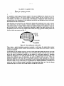
1. INTRODUCTION.
The ever growing complexity of very large scale integrated circuit chips demands tools to analyse
the spatial yield distribution of wafers and to relate this information to the particular layout for
fault prediction [131. [141. [171. [241. [261 and design yield estimation. Increasing the levels of
semiconductor integration to larger chips with more and more transistors addresses topics such as
the yield associated with individual process steps like etching. metallisation. etc. or the spatial
distribution of random and systematic sources of yield loss [271. [281. [291.
The actual prnduction wafers are an excellent source of information available at minimum effort
and low cost that reliably rellect the limiting factors existing in the technology process.
Interaction with these factors can be aided by analysing the wafer maps where functional.
nonfunctional and partially functional regions can easily be observed.
Bener circuit designs and yield improvements can be achieved by understanding the properties of
complete wafers and by redirecting these results exactly to the process and design stages where
they belong.
It is then necessary a tool to manage the enormous amount of data coming from the
manufacturing lines and to condense it in useful information for the process engineer. the layout
designer. the quality engineer. etc. or for whom yield prediction and estimation are very
important issues for the IC design' and process development.
It is well known that the local yield varies from wafer to wafer and that by examining batches of
wafers it is possible to correlate non functional circuits and their contributions to yield loss.
Sometimes it is desirible not only to an&lyse data but also to simulate the effect of density
variations in a wafer and between wafers. or to ex:erdse new yield models and compare their
results to real data.
.
For these and more reasons. the creation of a user friendly interactive environment is imperative.
This research i~ concerned with the development of tJ:e W<ifer Yield Editor ALWAYS (AnaLiser
of WAfer YieldS). ALWAYS is a me"u oriented system designed to analyse spatial distributions
of wafers. Graphical representations in the form of wafer maps. curves. and charts are used
extensively for user interface. Flexibility to create wafer masks. wafers. and chips of different
dimensions. as well as several miscellaneo:Js tools such as hardcopy. overlapping of extracted
wafer maps. etc., are provided. Simulation of wafer maps and yield vs. area predictions are also
available. And finally. data is read and stored in a very simple database structure.
All the algorithms through this report are shown in a C like syntax.
_. 2 -
2.
INPUT DATA AND! DATABASE DESCRIPTION.
The staning data is a set of wafer maps of wollong and nonwoIlting circuits of individual wafers
produced from the process of interest. The data gathered for the analysis can be collected from
electrical sort systems or by optically decoding the ink dot pattern placed on the wafers during
the sort procedure. This allows automatic plintout of the maps in an easy form for furthcr
manipulation of data.
Input data to the yield editor consists of all the die positions and their status. good or bad. of each
wafer in each lot for each project. We define a set of wafers as a lor anll a set of lors as a project.
This classification allows us to hierarchise die information. Hence. the database description
follOWS a tree structure where the parent is the product itself. the children represent each one of
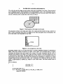
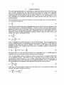
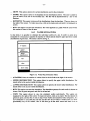
the lots of the product. and the grandchildren I'('present the individual w.afers for each lot. see Fig.
\. Since the information flows from grandparent to grandchildren a double linked structure is
unnecessary and thus we only have single connected lists. this saves some memory space in
defining extra pointers and simplifies the code since only one link has to be updated for deleting
or inserting elements in the list.
project
LOTl3B
lot
Hafer
11311.1 11311.2 113A.3
113B.l 113B.2 113B.3
Figure 1. (a)The information is hierar:hised in a tree structure. (b) An example.
Internally we place the dice in a square matrix. that we call the mask. The mask represents the
photolithographic mask of the technological process. Once that the pmjects. lots and wafers for
the analysis are selected it is easy to generate a general matrix which mntains the history of all
the wafers implied. Since ·the mask can be of arbitrary size. bigger or smaller than the wafer. it is
then necessary to prevent writing wmng information. this is done by checking if the die lays
inside of the wafer. The following routine shows how the tree structure is traversed in order to
obtain information from each wafer.
generate_workinlLwafer()
(
while( project...pointer != NULL) (
while ( lot...pointer != NULL) [
while ( wafer...pointer !,= NULL) (
for ( x = 0; x < total_dice_in_x; x++ ) I
for ( y ,= 0; y < total_dice_in..)'; y++ ) (
if( die_in_wafer(x.y» (
if (wafer...pointer->status(xJ[y] == GOOD)
composite_wafer[x][y] += I;
wafer...pointer" wafer...pointer->next;
- 3 -
10t-POinter = 10t-POinter->next;
project_ptr = project-ptr->next;
It is possible to make analysis between wafers of the same or different lots. between lots of the
same or different projects. and between different projects. Notice that the concept of project is
very flexible. it can mean i.e. a memory chip. a test structure. or simply the same memory chip
processed with a new equipment or new chemicals in which it was desirable to make a difference
between the new and the old process.
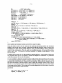
Input data does not necessary have to represent the absolute die coordinates in the wafer. Assume
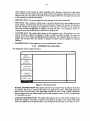
for a moment that a test chip contains a monitor to detect up to four multiple spot defects. If one
wants more accuracy or simply wants to reflect the number of defects it is possible to subdivide
the test chip in four. where each subdivision represents a defect The data could be now the
coordinates of each one of the new subdice and its status. let us say. good for a defect present and
bad for a defect not present. see Fig. 2.
Wiler
Figure 2. Dice configuration in the wafer.
Then. when a radial distribution analysis is executed. it will mean the radial defect density
instead of the original monitor density. and furthermore. accurate data as the number of defects
will also be obtained.
The flexibility in the database structure. as well as in the input data permits the user to cope with
almost any situation in spatial yield analysis. The only limits. thus. are restricted to the user itself
and to the type of information available for the analysis. A well known method of obtaining
significant information is by using test structures (22). (23) for process monitoring (10). This
implies that different types of information are used by different kind of users. When the
parameters supplied to the editor are. i.e. linewidths. resistivity. oxide thickness. etc .• then the
production stage can have impact on yield through a correct analysis procedure and an appropiate
corrective action. On the other hand. if the parameters are defect distributions. distribution of
opens and shorts in different layers. distribution of good and bad chips. etc .. then the design
engineering stage will benefit itself doing analysis through the yield editor.
.. 4 -
3.
WAFER SIZE AND DIE ASSIGNMENTS.
The wafer size and die shape are user entries which can be modified at any time. Dice are placed
on an imaginary square which represents the IlholOlilOgraphic mask 01' the fabrication process.
The shape of the dice can take the fonn of a rectangle of any size. and the center of the mask is
used as a reference point to center the wafer frame. see Fig. 2.
Figure 3. Wafer position with respect to the mask.
The placement of dice in the mask goes from left 10 right and from bottom 10 lOp. as shown in
Rg. 4. This is important since dice are clippe<ll to the wafer and partial dice are discarded. The
size of the mask is also adjustable to any value .
.. ..
'
'
.: t
Di. (~j)
...
. ..
Figure 4. Die arrangement in the mask.
Eximining whether a die is in or out of the wafc:r is a tedious algorithm because it is necessary 10
check if the four comers of the die lay inside of the wafer. The procedure that we employ
calculates the distance from each comer to th€: center of the mask. remember that the wafer is
centered with respect to the center of the mask. and then evaluates if all these distances are less
or equal than the wafer radius. The input parameters 10 this routine are l:he coordinates of the die
with respect 10 the left comer of the mask. To transfonn the coordinaU:s to distances we simply
multiply them by the size of the die in the x and y directions. For simplicity the flat side of the
wafer is approximated 10 O.04R [15l. where It is the wafer radius. The final routine looks as
follows
die_in_wafer(ij)
{
= die_size_x ... i;
x
= die_size-y * j;
y
*'
1* out of the mask 111
if ( x + die_size_x > mask_size 11 y + di,:_size-y > mask_size)
retum(OUTSIDE);
- 5 -
Oat
= 0.04 * wafer_radius;
lefCbottom_x = mask_center - ( x + displace_x );
lefCbottom-y = mask_center - ( y + displace_y );
left_top_x
= left_bottom_x;
left_top-y
= left_bottom_y - die_size-y ;
righcbottom_x = left_bottom_x - die_size_x ;
righCbottom_y = lefCbottom_y;
righUop_x = righCbottom_x;
righUop_y = left_top-y;
=
radius_Ib
sqrt (left_bottom_x * left_bouom_x + left_bottom-y • left_bottom_y );
radius_It
=
sqrt (left_top_x • left_top_x + lcfuop_y • left_top_y );
radius_rb
=
sqrt (right_bottom_x • right_bottom_x + righcbottom-y * right_bottom_y);
radius_rt
=
sqrt (righctop_x * righUop_x + righUop-y • righctop-y );
1* below the flat 11? • /
if (left_bottom-y > 0 && left_bottom_y > (wafer_radius - flat) )
return(OUTSIDE);
1* in the wafer ??? .... */
if ( radius_Ib <= wafer_radius && radius_It <= wafer_radius )
if ( radius_rb <= wafecradius && radius_rt <= wafecradius )
retum( INSIDE );
return ( OUTSIDE );
Some variables are redundant but they were left for a matter of clarity.
Fixing the wafer's center with the center of the mask does not always achieve the maximum
number of dice in the wafer, or simply it does not look like the "real life" wafer. However, the
availability of a mask wilh all the dice allows to "move" the wafer frame in order to obtain the
"real life" dice configuration. Thus the wafer can be shifted up, down, left or right through the
mask at user's will. Tl'e amount of shifting is speCified in displace_x and displace_y in the
previous routine.
In addition to the normal dice it is also possible to specify dead dice. The locations of these dice
are considered dead and are not taken in account for analyses or simulations. In production
wafers they represent the test sites for instance.
It is also possible to obtain the maximum number of dice in the wafer according to [151, see Fig.
5. In our case the parameters G and H are made to be less or equal to the size of the die in the
horizontal and vertical directions, respectively. The following routine finds the displacement of
the wafer with respect to the mask center in order to obtain the maximum number of dice. Notice
that this is a very expensive routine since it has to iterate die_sizeJ;*die_sizey*i* j times before
it can output correct results. The accuracy of the routine depends on the delta values, the smaller
they are the more accurate results we obtain.
maximumO
{
dice = max = max_x = max-y = 0;
displace_x = displace-y = 0;
- 6 -
for ( displace_x = 0; displace_x < die_size_x; displace_x += delta_x) (
for ( displace_y = 0; displace..)' < die_size..}'; displace_l' += delta..}' ) (
for ( i = 0; i < nwnber_dice_in_x; i++ ) (
for (j = 0; j < number_dice_in_y; j++ ) (
if ( die.Jn_wafer( i, j ) )
dice++;
)
if(dice>max) (
max
= dice;
max_x = displace_x;
max..)' = displace_y;
)
dice =0;
)
G
'"""..... ,....
~
... ~
,-,.
"B
T
-r
Figure S. Wafer displacemel~t from the center of the mask.
The final configuration of the wafer, i. e. the size, the dice's size, etc., is considered as the
prototype wafer and will be used in the analyses and simulations.
- 7 -
4.
THE MAP AND DISTRIBUTION ANALYSES.
The analysis is based on cumulative results by doing the Boolean And on a set of wafers. The
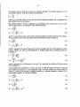
result is a composite wafer map which contains the cumulative yield by site location as shown in
Fig. 6. TItis methodology and its benefits were already reported for a specific application in [16]
and for a spatial analysis in [19]. We extend it by considering not only the individual wafer
variations but also by taking in account the lot and project variations of the product.
!'i~ure·S.
:he Boolean And of wafers.
an
In Fig. 7 we can see the typical fl.Jw of
analysis. TItis kind of wafer convolution allows also to
consider the mean and standard deviations between lots and between projects. a well known
problem [11]. Furthennore. the me\t.odology exploits the fact that wafers have statistically
dependent yield patterns for certain processing steps. and also that wafer yields are usually
correlated when processed in the sam~ lot or under similar conditions.
Figure 7. The convolution of wafers in a typical analysis
The within wafer yield variations are inspected by using the concept of site yield. A site yield
shows how many times in the complete set of wafers involved in the analysis a particular die
.. 8 -
accomplished a function. For instance, if our analysis consists of a lot of ten wafers and one die in
the composite wafer was only five times good, then its functional site yield is of 50%. Thus we
can write the site yield as
Fsiu
Y,", = -Nit-
(I)
where F,", is the site frequency, in other wonls the number of times that the die was projected,
and Nit is the number of wafers involved in the analysis.
It is obvious that by using this approach w(~ can account for wafer to wafer, and lot to lot
variations, as well as regional variations in wafers.
AL WAYS can execute two kinds of analysis on data. One is called the map analysis and the
other the distribution analysis. The map analysis displays the composite wafer map with the
projected dice that accomplished the function, and its purpose is mainly intended to see the
correlated spatial behaviour of the input data. The distribution analysis, on the other hand,
quantifies the behaviour of the input data by showing the curves of diffe:rent types of distributions
of the final composite wafer map.
The map analysis that ALWAYS can carry on nre:
+ Functional Map. The functional map shows all the die locations which were good all the
time in the whole set of wafers selected ~)r the analysis. Additionally, the correlated mean
and standar1 deviations between lots and projects is also evaluated for good dice. From the
practical point of view this map is useful in determining which are the most correlated dice in
a wafer in order to assure a minimum wafer yield for evaluating product costs, for instance.
+ Zero Map. The zero map shows all the die locations which were bad all the time in the
whole set of wafers selected for the analysis. As with the functional map the mean and
standard deviations 2re evaluated but this time is for bad locations. This map shows
immediately which are the dice detractors and major contributors to yield loss, one can also
observe from this map the least correlated "~gions in a wafer.
+ Up-range Map. This map shows all the die locations which showed a specific yield, or
above it, for the whole set of wafers. The correlated statistics are also evaluated for lots and
projects, i.e. the specified yield is also leoked up in every lot and in every project. The
specific yield is a user entry. We can use this map, for instance, to investigate the general
correlation of a specific process step a1on~: the entire lot Let's say that the input data were
process parameters, like the Vt of depletion transistors, then by asking to show the 50% site
yield, or more, we can infere about the uniformity of the ion implantation process step, for
instance.
+ Low.range map. This analysis shows the locations with a specific site yield or less. In
certain form this map is the complement of the previous one. An e.ample of its use is when
the input data are defect sizes, i. e. a die is good if the defect size measured for that location is
of a predefined value, otherwise it is bad. We can organise the data in such a way that one
project contains information of defects of size x and another project of defects of size y, and
so on. Thus, if we select only one project and we ask for the locations where the specific site
yield is SO% or less, we mean that we want to know the correlation of defects along the whole
set of wafers involved in the project. The result couid be interpreted as an index of how many
times defects of the same size showed to be clustered in the same place in half, or less, of the
total wafers involved in the analysis.
+ History map. This analysis shows numerically the yield of each die location for the whole
set of wafers. The uncorrelated analysis showing the mean and standard deviations between
- 9 -
wafers, lots, and projectS is displayed here. This numerical infonnation is useful to quantify
each site yield of the composite wafer.
+ Informative map. This is a contour infonnative map, it shows the average and the above and
below average site yield of the dice. Zero yield locations are distinguished from the rest of the
dice. This analysis allows to visualise the unifonn distribution of the type of input data in
question. For our previous example of Vts this map shows the scanning unifonnity of the ion
beam of the ion implanter, if there were doubts about the equipment, or the effectiveness of
the mask employed for this process step. For our example of defect sizes, this maps shows the
distribution of defects of a specific size along the wafer and through the entire lot.
+ Cluster map. In this analysis the user is asked to specify the number of elements that define
a cluster and the site yield for the dice. The resulting map shows the clusters according to the
previous specifications. Statistics such as the numbers of clusters and the number of clustered
dice are reported.
Lets investigate now into a bit more of detail the generation of the map analyses. The next piece
of code shows how do we find the functional map, however, this routine can easily be extended to
find the other map analyses. We make use of the fact that the infonnation is stored in a matrix,
thus we first check whether the element in tum of the matrix, in other words the die, lays inside of
the wafer and if it does whether it accomplished a hundred per cent yield. If both conditions are
satisfied we can proceed to proj'!ct the die by drawing it and also to update the computation of the
functional yield.
functional_mapO
{
for ( x =0; x < total_dice_in_x; x++ ) {
for ( y = 0; y < total_dice_in_y; y++ ) (
if (dic_in_wafer(x,y) ) {
if (composite_wafer[x)[y] == SITE_YIELD) (
draw_die(x,y);
functionaCyield++;
}
}
functional.sield = functional-Yield I total_number_oLdice;
In order to be able to fmd clusters in the wafer it is necessary to define clearly what a cluster
means. We define a cluster as a number of contiguos dice that have the same site yield. Thus,
clustered elements can be in the horizontal, vertical or even diagonal directions with respect to a
"seed element". The seed element is the die which was taken as a reference for the search of
contiguos dice. The routine that implements this search uses the principle of the "depth search"
algorithm.
The main idea behind this algorithm is to take one die that has the cluster yield specified and then
look if its neighbours also have the specified yield. Since the number of neighbours and their
directions is unknown it is necessary to check for the neighbours of the neighbours and then for
the neighbours of the neighbours of the neighbours, and so on. At first glance we see that this
routine is suited for recursivity. Next, to detennine whether the dice found fonn a cluster or not
we simply check against the number of elements that make up a cluster. This parameter is a user
entry, thus we can find clusters of one, two, or more elements. The next routine finds the dice that
- 10 -
have the same site yield and maries them in the "cluster wafer". This routine is part of a main one
where first the seed element is set and later it is investigated if the marked dice form a cluster by
comparing the number of cluster elements with the minimum number of elements.
find_clusters (x, y)
int x, y;
(
1* These are the cardinal points, i.e. NW is north west,
NO north, etc.
NW, NO, NE, WE, EA, SW, SO, SE, SEED "'
int xoff[9) = ( -I, 0, I, -I, I, -I, 0, I, OJ;
intyoff[9)= (-1,-1,-1,0,0, I, I, I, OJ;
cluster_map[x)[y) = mark;
cluster_elements++;
for (next = 0; next < 8; next++) (
neighbour_x = x + xoff[next);
neighbour...)' = y + yoff[next];
if (neighbour_x < 0)
neighbour_x = 0;
else
if (neighboucx > total_dice_in_x )
neighbour_x = total_dice_in_x;
if ( neighbour_y <
neighbour...)' = 0;
else
if ( neighbour...)' > total_dice_in...)' )
neighbour...)' = total_dice_in...)';
if «die_in_wafer(neighbour_x,neighbour...)'»
if (composite_wafer{nc:ighbour_x)[neighbour_J') == CLUSTER_YIELD)
if( c!uster_map[neighbour_x)[neighbou.r...)') != mark)
find_clusters(neighbour_x,neighbour...)');
°)
In order to account for the different density variations in the wafer, and to quantify the yield loss
we provide a radial distribution inspection [I), [4), [8) of the compos it,! wafer. Furthermore, the
combination of the radial analysis with an angular analysis [7) will facilitate us to observe the
behaviour of clustering. Another important wurce of information is a site yield frequency
distribution [2] that tell us how many times in the whole set of wafers involved for the analysis a
panicular die site was projected. Through thill analysis we can quantify the die correlation of
wafers and have a defined idea of correlated site yields. A natural consequence of the previous
analysis is a cumulative frequency distribution analysis [9) which ll:lls us about the overall
behaviour of the whole set of wafers, for instance we can see immediately the probability of
occurrence of each of the different site yields. Finally, an analysis which could not be omitted is
the yield vs. area [3),[ 12).
In the radial and angular analysis the user is al:ked to specify the site yield which is going to be
looked for. This adds Hexibility to the analysis, since in this form we C,iIl obtain a set of different
curves for different site yields. One example that makes use of this iidea is when we want to
analyse the frequency of ocurrence of defects in different regions of the wafer. So, we can obtain
radial or angular distributions for 0, I, 2, or N defects and each anal ysis independent of the other.
- 11 In the yield vs. area analysis the user is also asked to speciry the site yield. The kind of benelits
that we can obtain rrom this reature are i.e. the number or derects per area in order to classiry
clusters [5],[6J or simply the "traditional" yield vs. area curve.
A routine of interest is the generation or the radial distribution. The radial plots are made using
concentric rings of constant area to determine the site yield at a distance, from the center of the
wafer. If't is the inner radius and '1 is the outer radius of the ring, the area is kept constant by
taking '2 as
A = !t(d '2
=
rI)
~~ HI
Instead of incrementing tile angle in one degree we maximise the angle by obtaining the arc sine
of the hypotenuse of the die and tile radius of the wafer. This will give us the minimum
incremental angle for a full coverage of dice along the scanning line. We do the same for the
radial increment, in this case we take the minimum value between the size of the die in the
venical and horizontal directions. Since we deal with die sites, it is necessary to find the
coordinates of any die for any given x and y vector components of the changing radius. This is
carried on in the fmd_die_at_radiusO function where the vector components are convened to the
corresponding die coordinates. Finally, to avoid counting a die which was already considered
within the previous angIe and or radius, we simply mark it and skip it if necessary.
The next routine applies these concepts.
rad ial_distri bUlionO
(
area = PI • (waferJadius)' (wafer_radius) /10.0;
rl = 0;
r2 = sqn ( area / PI );
squared_x
= die_size_in_x • die_sizejn_x;
squarcd_y
= dic_sizc_in_y
* dic_sizc_in_y;
die_size = sqn ( squared_x + squared_y );
delta_theta = asin ( die_size / wafer_radius);
delta_radius= MIN( die_si],e_in_x, die_size_in_y );
do (
radial_yicld = elements_found = 0;
for ( theta = 0; theta < 2 • PI; theta += delta_theta) (
for ( radius = rl; radius <= r2; radius += dcltaJadius ) (
x = radius' cos( theta );
y = radius • sine theta );
fmd_dic_auadius( &x,&y );
if( radial_mark[xJly] == FALSE) (
radial_mark[x][y] = TRUE;
c1cmcnts_found++;
if ( composite_wafer[xJfy] == SITE_YIELD)
radial_yield++;
plot ( r2, radial_yield / elements_found );
rl = r2;
r2 = sqn ( area / PI + ( rl • rl ) );
) while ( r2 <= wafer_radius);
- 12 -
S.
THE STA TISTICS.
The wafer maps standing alone are a good means to display the regional distribution of the input
data on wafers. Although they are a good tool they are usually not enough. One is generally
interested in quantifying the results in order to make conclusions of the analysis, i.e. to know the
yield of good dice, the variations of good dice between wafers, etc. It i:; thus necessary to count
with a minimum set of statistical infonnation as to make inferences about the wafer or set of
wafers in analysis.
The first infonnation is the yield of the function, i.e. the yield of good dice, the yield of bad dice,
etc. This yield is evaluated as
Nt
YF = -
(2)
Nc
where Nt is the number of dice that accomplisht:d the function and Nc is the total number of dice
of the composite wafer, excluding the dead dice. It is also of interest to find how did the function
perfonned in each lot and in each project. Thus, for each function we give infonnation about the
mean yield per lot, and per project, with their t:Orresponding variances. Each partial yield is an
independent random variable and altogether constitute a random sample for whose mean Xp and
variance s~ are given according to [25 J by:
1 i:IV
Xp
=-
LYi
(3)
N i=1
I i=N
s~ = - - L(Yi - xp)2
N - 1 i=t
(4)
where Yi represents each partial yield and N is the size of the sample. These two quantities give
an idea of the perfonnance of the function per lot or per project. Furthennore, a 95% degree of
confidence of the mean yield value is evaluated. If Xp and Sp are the values of the mean and
standard deviation of the sample of size N, then the (1 - a) 100% confidence interval for the
population mean y is:
Xp -
t.E:...
Sp
N
Sp
_l--<Y<xp + t!!:....,N _ 1 - -
2·..fN
(5)
2..fN
This means that if we had more lots, or projects, we could assert willI (1 - a) 100% degree of
confidence that the true average lot yield is between the two boundaries.
Since the methodology exploits correlation of wafers we also provide an expected value of dice
and its standard deviation. This expected value is the mean of the distribution of dice that
accomplished a specific function. If z is a rar.idom variable representing the site frequency, in
other words the number of times that a die can accomplish the function, and f (z) is the number of
dice that exhibit the site frequency in the composite wafer, then the mean is given by
Il =
,:IV... f (z)
L z--
z=1
(6)
Ndice
where Ndie< is the tOlal number of dice in the wafer, and
analysis. The standard deviation is given by
,:IV...
a =(
L
2'=0
Nwaf"
is the number of wafers in the
I
f( ) 2'
(z - 1l)2_Z_)
Ndice
(7)
- 13 -
The statistics that we showed so far are for correlated functions. The history map has a set of
uncorrelatcd statistics. First, the yield here is evaluated as
Ng
Yu = -
(8)
N,
where Ng is the total number of dice that were good during the analysis, and N, represents the
total number of dice in the analysis.
The variation between wafers is inspected by evaluating the yield of good dice in each wafer.
Then the mean yield x'" and variance s~ for wafers is given by
1 iooN
~=-~~
N
00
i=1
1
iooN
= - _ ~(Y· -x )2
" ' N l- ' &
i=1 " ' ' ' '
S2
(10)
where Yi is the yield of each wafer and N is the total number of wafers involved in the analysis.
The uncorrelated mean yield and variance for lots and projects is also evaluated as
1 iooN
X
= -~Yi
S2
N
(II)
i=1
1 iooN
= - - ~(Yi - x)2
N - 1 i=1
(12)
where Yi represents Ihe yield of good dice in Ihe lot or project, and N the total number of lots or
projects. Finally, the mean of Ihe distribution of wotting chips and its standard deviation is
evaluated as
(13)
(14)
where x represents Ihe site frequency of a die and f (x) represents Ihe number of dice that exhibit
Ihe site frequency.
Cluster statistics are considered in a similar way. First we find !he number of clusters C and Iheir
total number of elements G in Ihe composite wafer. We also evaluate Ihe mean number of
clusters Xc and Ihe mean number of clustered elements Xu, wilh their respective variances s; sb,
per lot and per project. This is done as follows
(15)
(16)
(17)
(18)
- 14 -
where Co represents the number of clusters Go the number of clustered clements and N the si7-c of
the sample. i.e. the number of lots or projects. A 95% confidence interval for the mean number of
clusters and of clustered elements is also eval~.ated.
This minimum set of statistics allows us to inspect the variations between wafers. lots and
projects.
- 15 -
6. SIMULATIONS.
AL WAYS provides two kinds of simulations. One is the evaluation of the yield vs. area and the
other is the creation of wafer maps. The yield vs. area is evaluated using a distribution of the
number of defects per chip, and its formula is given according to [12J as:
,
2
Y = [(AD(.!!.)
11
.(.lO.)
+ 1)]
(19)
"
where A is the area of the die in the prototype wafer, D is the average defect density. and
~ the
11
coefficient of the defect density variation. In this simulation the user is able to give the mean and
the standard deviations as input data or. to create a file containing the description of the
distribution to be used. or can draw the distribution online.
The wafer map simulation is for one lot. The number of wafers in the lot is a user entry. and the
characteristics of the wafer correspond to the prototype wafer. The input data to simulate wafer
maps consists of the relative radial distribution of site yields. expressed as follows
Ng
YR = -
(20)
NR
where Ng is the number of good dice at radius R and NR is the total number of dice at radius R. It
is clear that the within wafer variations are considered with a radial distribution. Now. in order to
consider the variations between wafers, one has to bear in mind that some wafers exhibit a higher
radial yield and some a lower. Therefore. the input data consists in fact of two radial
distributions. one for the upper bound and the other for the lower bound. Thus the regional
variation of the simulated wafers lays between these two limits as
Ii = YR. - YR,
(21)
where YR. is the upper radial yield and YR, is the lower radial yield. both at radius R. Hence. the
simulation is left to the task of generating a random number of good dice for whose relative radial
yield at wafer radius R lays between these twO boundaries,
The next routine applies the former idea. The input parameters to the routine are the partial radius
and the number of dice at that radius. This routine forms pan of a main loop in which the the
partial radius is incremented from zero to the wafer radius and that for each partial radius the
correponding number of dice is found.
simulate_radial_dice(radius.numbecdice)
(
if (upper_yield(radius) < lower_yield(radius) ) {
errorO;
retum(F ALSE);
]
good_dice = upper_yield(radius) * number_dice;
= good_dice - lower_yield(radius) * number_dice;
bias
!* generate the number of good dice randomly"'
random_dice(number_dice,good_dice.bias);
!* place the generated good dice
*'
random-piacement(radius,numbecdice);
retum(TRUE);
.. 16 -
As with the yield vs. area simulations the distributions can be givcn in a file or can be drawn
directly on screen. After the wafers are created it is possible to e"aminc each one of them and
also to perform any of the map analyses on the composite simulated wafer. In these simulated
maps the only statistics reponed are the yield of the function and the mClm and standard deviation
of dice for the function.
As a final remark, recall that the input data implies site yields. Thus, the map interpretation
depends on the interpretation given to the site. l"or instance, if the site yield represents a defect of
a specific size .t, then the wafer simulated wi.ll show the regional distribution of defects. Of
course, the radial distributions represent the rallial yield of defects at radius R, and, the smaller
the die size the more accurate the simulation il;, since in this case it represents the position of a
defect in the wafer.
- 17 -
7.
SUMMARY AND CONCLUSIONS.
Standard tools of statistical means of control have been available for many years. However, their
use on a routine basis ha~ been somewhat limited. This is due mainly to a lack of easy access to
the appropiate data, the tedious hand plotting of chans or wafer maps and the difficulty of
keeping an up to date on line system. Hence, it is essential that this capabilities be accessible in
an easy form [18].
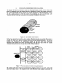
AI.WAYS provides interactive graphics displays, online screen reports, hardacopy plots, and
facilities to store in the database the analysis or simulation just performed. as well as to retrieve
previous ones. These analyses can be overlapped over the current composite wafer to do
comparisons or simply be placed instead of the current map.
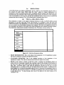
As a part of the user friendly interface a set of color graphics to repon wafer maps and
distribution charts was included, see Fig. 8. Also any distributions for the simulations can be
drawn online. lbis feature eases the continuos execution of quick simulations for new user's data.
a
••00
000181ii81iiiio
••0•••••00
iil=iiII181~81
••
.~ •••• o ••
.0.0 •• 0.000
0.0.000.0 •• 0
• • 0 • • 0000.
0 •••••••
00 • • 00
.....d.....
y ....
....
....
•
..
"•
frvja:t •
....••
12
16
20
za
24
:z
J6
I
~
~,
"-
~
'0
.,••
"-
0.6
"
~
g
1"
I
1 0.'
.,
1\
u
~
\
"
1
Di~l.ancc
0.'
.,
"
from wafer's cenler
Figure 8. (a)Example of wafer maps. (b)Example of distributions.
To facilitate access to the results of every map analysis, the statistics are reponed immediately to
their right. They include the yield of the composite wafer, the number of projects, lots, wafers,
and dice involved in the analysis, and the yield variation between lots and between projects.
AI.WAYS is a program winten in C and implemented on an Apollo Domain 3000 Workstation
System running Unix 8S04.2. The current version supports static menu screens but later
versions will provide pop-up menus. It is not a disadvantage to have static screen menus when the
number of nested menus is small, although, the ever increasing availability of UIMSs [21 J
promotes an upward to this kind of interfaces. Future work involves providing facilities to have
dice of different sizes in the same wafer and also facilities to correlate wafers with dice of
different sizes and shapes, among others.
- 18 -
We presented a simple, yet complete, package for wafer yield analysis. As in every beginning,
things are not that easy. When there were no ]ayout editors, people used to do their designs by
hand, or by creating isolated programs to easy this enormous task, suddenly the first layout
editors appeared and became more and more popular up to the point where nowadays it is an
indispensable and easy to obtain tool. Similarly, the idea of the Wafer Yield Editor shows that it
is easy to construct a system to help in the analysis of yield improvement. Sophisticated CAM
tools [20] that provide statistical process and q~lality control, and, analysis and simulation of yield
management are also available. However these systems are oriented to automate the wafer
processing in silicon foundries and their scope differs from yield analysis. ALWAYS is an
example of a tool for research of yield analysis which everybody can make at little expense.
ALWAYS is not only suited for usage in the silicon foundry but also) in the layout designers
rooms, the theoretical yield modelers office, etc.
The most significant features of AL WAYS arc :mmmarised as follows:
I) A simple database structure allows to exam'lne lOIS, and individual wafers.
2) Full flexibility to edit the characteristics of Ine prototype wafer.
3) The analysis techinique allows to estimate the contributions of both correlated and
uncorrelatcd detractors to the total yield. SI~ch information can be llsed to study the effect of
process changes on product yield.
4) Simple simulation tools to estimate the
waf'~r
yield.
It is our believe that a simple package like ALWAYS provides a positive impact on yield
improvement.
- 19 REFERENCES
[1]
Ham, W.E.
Yield-area analysis. Part 1: A diagnostic tool for fundamental
integrated-circuit process problems.
RCA Rev., Vol. 39(1978), p. 231-249.
[2]
Warner, Jr., R.M.
Applying a composite model to the IC yield problem.
IEEE J. Solid-State Circuits, Vol. SC-9(1974) , p. 86-95.
[3]
Stapper, Jr., C.H.
On a composite model to the IC yield problem.
IEEE J. Solid-State Circuits, Vol. SC-10(1975) , p. 537-539.
[4]
Ferris-Prabhu, A.V. and L.D. Smith, H.A. Bonges, J.K. Paulsen
Radial yield variations in semiconductor wafers.
IEEE Circuits & Devices Mag., Vol. 3, No. 2(March 1987), p. 42-47.
[5]
Stapper, C.H.
On yield, fault distributions, and clustering of particles.
IBM J. Res. & Dev., Vol. 30(1986), p. 326-338.
[6J
Stapper, C.H.
Yield model for fault clusters within integrated circuits.
IBM J. Res. & Dev., Vol. 28(1984), p. 636-640.
[7J
Gupta, A. and W.A. Porter, J.W. Lathrop
Defect analysis and yield degradation of integrated circuits.
IEEE J. Solid-State Circuits, Vol. SC-9(1974), p. 96-103.
[8]
Yanagawa, T.
Yield degradation of integrated circuits due to spot defects.
IEEE Trans. Electron Devices, Vol. ED-19(1972) , p. 190-197.
[9]
Stapper, C.H.
Defect density distribution for LSI yield calculations.
IEEE Trans. Electron Devices, Vol. ED-20(1973) , p. 655-657.
[10J
[llJ
Stapper, C.H.
LSI yield modeling and process monitoring.
IBM J. Res. & Dev., Vol. 20(1976), p. 228-234.
Stapper, C.H.
The effects of wafer to wafer defect density variations on
integrated circuit defect and fault distributions.
IBM J. Res. & Dev., Vol. 29(1985), p. 87-97.
[12J
Stapper, C.H. and F. Armstrong, K. Saji
Integrated circuit yield statistics.
Proc. IEEE, Vol. 71(1983), p. 453-470.
[13J
Walker, H. and S.W. Director
VLASIC: A catastrophic fault yield simulator for integrated
circuits.
IEEE Trans. Comput.-Aided Des. Integrated Circuits & Syst.,
Vol. CAD-5(1986) , p. 541-556.
- 20 [14J
Walker, D.M.H.
Yield simulation for integrated circuits.
Ph.D. Thesis. Pittsburgh, Pa.: Carnegie-Mellon University, 1986.
[15J
Gupta, A. and J.W. Lathrop
Yield analysis of large integrated-circuit chip!;;.
IEEE J. Solid-State Circuits, Vol. SC-7(1972) , p. 389;-395.
[16J
Calhoun, D.F. and L.P. McNamee
A means of reducing custom LSI interconnection :requirements.
IEEE J. Solid-State Circuits, Vol. SC-7 (1972), p. 395-404.
[17J
Maly, W. and F.J. Ferguson, J.P. Shen
Systematic characterization of physical defects for fault
analysis of MOS IC cells.
In: Proc. 15th Int. Test Conf., Philadelphia, 16-18 Oct. 1984.
New York: IEEE, 1984. P. 390-399.
[18J
Campbell, D.M. and Z. Ardehali
Process control for semiconducting manufacturinq.
Semicond. Int., Vol. 7, No. 6(June 1984), p. 127-131.
[19J
Mallory, C.L. and D.S. Per1off, T.F. Hasan, R.M. Stanley
Special yield analysis in integrated circuit manufacturing.
Solid State Technol., Vol. 26, No. 11 (Nov. 1983), p. 121-127.
[20J
Burggraaf, P.
CAM software. Part 1: Choices and capabilities.
Semicond. Int., Vol. 10, No. 6(June 1987), p. 5':'-61.
[21J
Myers, B.A.
Creating interaction techniques by demonstratio::1.
IEEE Comput. Graphics
p. 51-60.
[22]
&
Appl., Vol. 7, No. 9 (Se:?t. 1987),
Maly, W. and M.E. Thomas, J.D. Chinn, D.M. Campbell
Double-bridge test structure for the evaluation of type,
size and density of spot defects.
Pittsburgh, Pa.: SRC-CMU Center for Computer-Aided Design,
Department of Electrical and Computer Engineering, CarnegieMellon University, 1987.
Research Report No. CMUCAD-87-2.
[23J
Chen, I. and A.J. Strojwas
A methodology for optimal test structure design for statistical
process characterization and diagnosis.
IEEE Trans. Comput.-Aided Des. Integrated Circuits & Syst.,
Vol. CAD-6(1987) , p. 592-600.
[24J
Chen, I. and A.J. Strojwas
Realistic yield simulation for IC structural failures.
In: Digest of Tech. Papers 4th IEEE Int. Conf. on Computer-
Aided Design (ICCAD-86), Santa Clara, Cal., 11-13 Nov. 1986.
New York: IEEE, 1986. P. 220-223.
- 21 [25]
Freund, J.E. and R.E. Walpole
Mathematical statistics 3rd ed.
Englewood Cliffs, N.J.: Prentice-Hall, 1980.
a
Prentice-Hall mathematics series
[26]
Chen, I. and A.J. Strojwas
Realistic yield simulation for VLSIC structural failures.
IEEE Trans. Comput.-Aided Des. Integrated Circuits & Syst.,
Vol. CAD-6(1987) , p. 965-980.
[27]
Fantini, F. and C. Morandi
Failure modes and mechanisms for VLSI
res:
A review.
lEE Proc. G, Vol. 132(1985), p. 74-81.
[28]
[29]
Edwards, D.G.
Testing for MOS IC failure modes.
IEEE Trans. Reliab., Vol. R-31(1982) , p. 9-18.
Taylor, R.G. and E. Stephens
Microcircuit failure analysis.
Sr. Telecommun. Eng., Vol. 4(1985), p. 39-46.
ALWAYS
User's Manual
CONTENTS
1.0 A Tutorial
1.1 Getting Started
2.0 User's Manual .
2.1 User Interface
2.2 Main Options
2.3 Wafer Editing
2.3.1 Wafer Displacement
2.4 Input Data Selection
2.5 Yield Analysis .
2.5.1 Wafer Map Analysis
2.5.2 Distribution Analysis.
2.6 Simulations
2.6.1 Yield vs. Area Simulation
2.6.2 Wafer Simulations
2.6.2.1 Radial Distributions
2.7 Miscellaneous Tools
3.0 Diagnostics and Troubleshooting
3.1 User Diagnostics
3.2 System Diagnostics
2
6
6
9
10
1\
12
13
13
14
16
16
17
18
19
20
20
21
-I -
1.
A TUTORIAL.
This section is not intended to give an exhaustive explanation of ALWAYS, it is rather aimed to
demonstrate the essential features of ALWAYS in a nonnal session, but without getting down
into fonnal rules. For more details refer to the report or to the user's manual. This tutorial
assumes that the user is seated behind a tenninal with ALWAYS running. The tutorial example
is located in the directory PATH/always.tutorial.
The wafers to be analysed consist of a sequence of tests to evaluate the threshold voltage
adjustment at EFFIe·. Four lots are derived, two are for depletion transistors and the others for
enhancement transistors. Thus we created two projects, one is called "depletion" and the other
"enhan".
EFFIe uses wafers of 3 inches of diameter, and the size of the dice in question is 5.8mm by side.
The results of the measurements are stored in a directory named PATH/measurements. We
created a filter to interpret these results for ALWAYS, first we evaluate the average and standard
deviations of the threshold voltages in each wafer, then knowing these values we make a process
window of acceptance of the voltage value. We say that the threshold voltage is good if its value
lays within -30 and +30 of the average value. Next, we simply pass from the coordinate system
of the ATE to ours for more convenience and simplicity. Fma1ly we repeat these steps for each
one of the wafers.
As a word of comment, all the wafers were not processed identically, some variations, as the
concentration of dopants, were changed. Hence, in the following discussion we avoid making
any statistical inferences of the results. We simply use them to show some of the features of
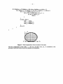
ALWAYS. The "real life" configuration of the dice in the wafers to be analysed is shown in Fig.
I.
Figure 1. Dice configuration in the EFFIe wafers.
•
Eindhovense Fabricage Faciliteit voor gelntegreerde Circuits.
(Eindhoven Fabrication Facility for Integrated Circuits.)
-2-
1.1
GETTilNG STARTED.
Start ALWAYS by typing
always <CR>
As we already mentioned, ALWAYS stands for "AnaLyser of WAfer YieldS", the current version
is 1.0, we hope to make more improvements. Now try clicking the Iefl bUllon of the mouse. This
button is used to point at any of the menu selections, the bUlton in the center is used to show
analyses previously stored and the button to the right is used 10 exit the program, this can be done
by doubleclicking it.
You are now facing the main menu optiom: of ALWAYS. At the top are displayed the
characteristics of the protoypc wafer, and as we can see they differ very much from our "real life"
wafer.
Move the cursor to the edil option and click the left button. This menu allows 10 edit the
characteristics of the prototype wafer. First we know that our dice are biggcr, thus click in the
die size option, you will be asked to enter the horizontal and vertical dimensions of the new die.
Now change the size of the wafer 10 76mm by dicking in thc wafer size option and entering thi,
new value.
So far we already havc the correct wafer and dice dimensions but thc configuration is still
different. The filter program that we mentioned, assumes that the rightmost die and closest to the
flat side of the wafer has coordinates (8,0). We can investigate which are the coordinates of this
die, or any other, by clicking in the XIY option and then clicking in the die iL~clf. The mask size is
73mm, thus, we need to displace the wafer 1.60110 to the right and 1.6mm down from the center
of the mask.
Adjust first the mask size by clicking in the mask size option and enter the new dimension, and
later switch to the adjustment menu by clicking in the adjuslment option. Set here the step size to
OAmm and then move 'the wafer four times to the right and four times down. Of course you are
free to give any other step size of your choice.
Now we are able to proceed with the analysis. The red bar down to left of the screen is the
"done/exit" bar. Clicking once in this bar we will return to the edit menu, and clicking again it
will position us back in the main menu.
Let us select now the data for the analysis. Click in the scI option. We are facing now the "set"
menu which allows us to set projects, lots and wafers for our analysis.
Let us pick up first the enhancement data. Click in the projecl option. To the right of the screen
are displayed all the projects that are present in the current directory. In our case there arc only
two. The "depletion" and the "enhan" projects. Since we said that we arc going to analyse first
the enhancement data click in the selecl option ,1Od then in the "enhan" project. The name of the
project should have been highlighted, otherwisl: try again. Now click in the "done/exit" bar 10
indicate that we want that project; this last action is interpreted as "done" with the menu and
"exit" it, so we are positioned again in the "set" menu. Now let us choose the loIS.
Click in the lOIS option. In a similar fashion 10 the projects, the lots arc displayed to the right of
the screen. These lots arc the lots that belong 10 the project previously chosen, that is, project
"enhan". Select the lot 5600. We have now the project and the lot for our analysis. Try to select
wafer 5600c 1 by doing similar operations to the project or lot selection.
Click in the "done/exit" bar until we get back to the main menu again. Now you will sec in the
three small windows to the right the project, lots, and wafers involved for the analysis.
"
-3 -
We have now the correct prototype wafer and we already chose the data for the analysis, so let us
analyse this data. Click in the analysis option, at the bottom you will see displayed a message
informing that ALWAYS is loading the data corresponding to the wafer 5600e l. After the
loading is completed we can face then the "analysis" menu. Remember that we selected only one
wafer, thus some options will be meaningless, although you arc free to try them.
We will find first all the good dice in the wafer, so, click in the functional map option. The dice
displayed in green arc the good dice, the rest are blank. To the right are some statistics. Mainly
they arc the yield of good dice, the number of projects, lots and wafers involved in the analysis,
the average lot yield, the variations in the lot yield, the project average and variation yield and
finally the expected number of dice that accomplish the function. Since we have only one wafer,
one project, and one lot, the project and lot variation values are the same.
Now find the bad dice, thus click in the zero map. The dice in red arc the bad dice. To the right
arc also displayed statistics corresponding to this map. The yield shown is now for bad dice.
Click now in the distribution option to check the radial and angular distributions of this wafer.
Click first in the radial option, you will be asked to give the site yield, type 100 to mean that we
want to find the radial distribution of good dice.
Now let us see the angular distribution, click in the angular distribution option and answer also
with 100 for the site yield.
If you try a number other than 100 or 0, ALWAYS will try to adjust it with respect to the number
of existing wafers in the analysis, for instance if you type 75% there is obviously no 75% yield,
there is only 0 or 100% since we have only one wafer. Thus, ALWAYS will respond with the
analysis for 0%. Remeber that our interpretation of site yield implies the number of projected
dice, from all the wafers, that accomplish a function.
At this point we assume that you arc already more or less familiar with the selection of data, so
let us add more data to the analysis. Click twice in the "done/exit" bar to go back to the main
menu. Now go to the "set" menu and select all the wafers of the lot 5600. So, click in the wafers
option then click in select option and then click through each one of the wafers, after you have
selected all the wafers click in the "done/exit" bar to indicated that we want all those wafers
(done) and that we want to go back (exit). Now select also all the wafers oflot 5500. Click in the
Jots option and then in the select option, then click twice in the 5500. This last action will select
all the wafers of lot 5500 because AL WAYS allocates, when two projects or two lots are selected
inmediately one after each other, all the elements of the secood to last selected item.
Now go again to the "analysis" menu, so click in the "done/exit" bar and then in the analysis
option. Let us investigate one of the variable maps, click in the up-range map and answer with 50,
this means that we want to see the dice that were good through half or more of the wafers in the
analysis.
Now click in the "distributions" option and then click in the "frequency" option, this last option
will display a histogram of the frequency of occurrence of each site yield.
Before we continue it would be good that you investigate the several options for the analysis by
yourself. Take your time ...
We shall see now the different tools that we have in ALWAYS, so place yourself in the main
menu and click in the tools option. Click now in the retrieve option, this option will display, and
allow you to select, analyses previously stored in the database, you will see only one called
"560le", which is the one that we created for the purposes of this tutorial. Click in the name of
the analysis to retrieve it. On screen you will see the characteristics of the analysis. It is a
·4-
functional map of one of the wafers. Now click in the overlap option. This action enables, as its
name says, the "overlap" function. That is, whenever we are dealing with any analysis and we
want to do an overlap of wafers between the rel.rieved from the database and the one created from
the analysis we usc this function, and if we want to swap wafers we ~.se the "alternate" option.
Now, click in the "done/exit" bar to go back to the main menu and then click in the analysis
option.
Choose now the info-map, so click in there, nnd after the analysis is finished click the middle
bunon of the mouse. This action will overlap the wafer that we have just retrieved over the info
analysis. The combination of an individual wa(cr and the info-map of all the wafers allows to see
the contribution to yield improvement or detraction of the single wafer.
The overlap and alternate functions act as toggles, so to get the initial info-map click again the
middle button of the mouse and see how docs tile retrieved map disappear.
The last feature that we arc going to review is the wafer map simulation. Go to the main menu
and click in the simulate option and then click in the wafer map option. In order to simulate wafer
maps we must provide the number of wafers to be simulated, the upper radial yield and finally the
lower radial yield. If any of this conditions is missing the simulation will not run.
Now, let us say that we want to simulate a lot (If 10 wafers. Click in the # wafers option and then
type 10 in the field to the right of the screen. Click in the upper distribution in order to set the
upper radial yic:d. A new menu will appear, click in the retrieve option. This option retrieves all
the distributions existing in the database. In this case there is only one., the "upper". Click on its
name and wait until it is drawn on screen, at that moment ALWAYS knows already which is the
upper yield distribution. We arc missing only the lower yield. Click in the "done/exit" bar to go
backwards and then click in the lower distribution option.
ALWAYS provides several mechanisms to capture a distribution, we already tried one, the
retrievement, another one is to create the ditlibution file in advance by typing it, and the last
alternative is to draw it directly on screen. We !:halltry this last option.
Click in the draw option. AL WAYS paints a grid whose ordinate is the wafer radius, and the
absice is the radial yield. Try to draw the distribution shown in Fig. 2. First click in the grid at
coordinates (0,0.6), they arc also displayed at the right side of the screen, this is the initial point, a
rubberband for line drawing will appear, direct the rubberband to the next point and click there,
the rubberband should have been fixed up to the new point and a new rubberband starting at the
last point appears. Continue to do so until YOIl finish drawing the distribution. If you commit a
mistake click the middle bunon of the mouse to undo the last line. To finish drawing click in the
"done/exit" bar.
-5 0.66
I ___ ~_' [--
D$
r- -.~-----
'.52
I -:.. I
0.48
f-- ..
T
!
0.39
0.33
l.
0.13
I
i.
3,8
7.6
1U
15.2
19.0
22.0
2$.6
30.4
34.2
38.0
Dlaance lrom Wafer centM
Figure 2. Lower relative radial yield for the example.
Now let us run the simulation, so click in the run option. The simulation phase starts
automatically and every wafer is displayed. After the simulation is finished the wafers can be
viewed through the view option and also they can be analysed through the show map option.
These analyses are the same that we investigated before.
From now on you are on your own, have an enjoyable time with ALWAYS, and good luck!!!
-6 -
2
US1~RS
MANUAL
ALWAYS is a system used for spatial yield estimation and prediction of wafers. It is able to
quantify yield variations between lots of wafers and between the wafers themselves by doing
wafer map and distribution analyses. Its features are explained in detail through the rest of this
manual.
2.1
USER INTERFACE.
AL WAYS assumes that the current directory contains all the proj(:cts to be analysed. The
taxonomy of ALWAYS is shown in Fig. 3. In it are shown in detail the options of the system and
the nesting levels of the menus.
"LWAYS
SiJD.u1Kion
r...jod
LoI
Wal.
I\..di.al DisIn"Wion
... .JuDUbiWion
CUll.. Distzibulian
Frcqv:Iq' Disbibution
YieIcl V$. Ala.
-- Wdame
M.,t_
Die_
....jalaent
Cent..
S". liIe
Up
DOwn
~
o~
Sloft
.
a........ AnoJysio
Slwll
....
......
Yield. \IS.
....omoIc
M..,.
~
s_
IleYioIlon
Dnw
5ho.
510..
Rdzilve
II...
IloooI di<o
Wafer Map'
aWahn
~n
( ..V)
Lo_
11_
IlAw
5h>w
5'...
,..-.
Z...
~
] am
Vlow
ShowMq
Up" lUllLO.... Allle
C=:r.ai¥e
CIuIor
~n
C. .vWlue
DisbiWion
Yidd ...
.....
Figure 3. Taxonomy of ALWAYS.
The following are the interfaces required to work with ALWAYS.
-
MOUSE INTERFACE. ALWAYS is a highly interactive system that makes use of mouse
based interface systems. The left button of the mouse is used to point at any of the options of
the menus. The bunon in the middle is ;n effect when the "overlap" or "alternate" options are
enabled or at the moment of capturing information in the "simulation" menu. The bunon to
the right is used to exit ALWAYS at any m"me:lt by doubleclicking it.
-
DONFJEXIT BAR. In the lower left comer of the screen a red bar called the "done/exit" bar
is constantly displayed. This bar has two effects. one is to confirm any operation realised in
-7-
the menu, such as to capture data cUNes in the simulation menu, and its other use is to go one
menu backwards. For instance, if it is desired to go back from the "adjust" menu to the main
menu, then by cliCking once on the bar, AL WAYS positions itself in the "edit" menu, and
then by clicking on the bar again, the main menu is achieved.
-
INPUT FORMAT. The input data of ALWAYS consists of the status, good or bad, of each
die in every wafer for all the lots and projects to be analysed. The "project" and the "lot" are
directories and the "wafer" is the file characterising the information. The project directory has
to be as follows :
projeccname .pro
the lot directory like
lot_name Jot
and the wafer file as
wafer_name .waf
The data in the wafer file is given as coordinates with the status of the die, the format is as
follows:
(x,y)= 1
for good dice, or
(x,y)=O
for bad dice, x and y represent the coordinates of a die inside the wafer.
-
ERROR REPORT. If there were errors in the wafer files, ALWAYS generates a file
containing information of these errors, i.e that a die is out of the wafer, or out of the mask,
etc. The name of this file is
"always.errors".
Mistakes comitted during the session are reported in the interface line, this kind of errors are
for instance an invalid die size, or trying to select a lot without having selected a project first,
etc.
-
INVOCATION. ALWAYS has also a configure file that presets the size of the wafer, of the
mask and of the dice. The name of this file is
"config.always"
and its syntax is as follows :
wN
mN
x N
yN
hN
vN
where N represents the size in all the cases, and
w - wafer size
m - mask size
x - die size in x direction
y - die size in y direction
h - wafer shiftment with respect to the mask in x direction
v - wafer shiftment with respect to the mask in y direction
These options can also be given interactively at the moment of starting ALWAYS as:
always owN -mN -xN -yN -hN -vN -i
The -i option is to tell ALWAYS to ignore the configure file, if it exists.
-
DATABASE FILES. Every analysis stored by ALWAYS with the "store" option in the
tools menu is characterised by
•
··8-
analysis_name .ana
and in the simulation section by
distribution_name .lIst
The analysis file is a non ASCII file and
file is
tllUS
x f(x)
where
x - domain of the function
f(x) - the function
Both files are stored in the current directory.
is not readable. The fonnat of the distribution
-9 -
2.2
MAIN OPTIONS.
This is the main menu of the system. From here it is possible to edit a wafer, to select the data for
the analysis, to carry on an analysis, to make simulations, and to use the miscellaneous tools. The
main menu screen is shown in Fig. 4.
At the top are displayed the characteristics of the prototype wafer. These characteristics are the
size of the wafer, the size of the mask, and the size of the dice. At the right are three small
windows named PROJECf, LOT, and WAFER respectively. These windows contain the
information of the data involved for the analysis. If the name of a project is clicked, all its lots
and all its wafers are highlighted, furthermore, if one clicks at one of the lots of the project all
the wafers that belong to that specific lot will be highlighted. It is possible to scroll in each of the
windows by clicking in the arrows.
Figure 4. Main menu.
-
SET. This option allows to select, or to cancel, projects, lots and wafers for the analysis.
-
ANALYSE. This option allows to carry on several types of analyses on the wafers selected
for this purpose.
-
SIMULATE. This option allows to simulate the yield vs. area or to simulate wafers maps
based upon the characteristics of the prototype wafer.
-
EDIT. This option allows to edit the characteristics of the prototype wafer
-
TOOLS. This option is used to save or retrieve data in the database, and to use other tools.
· 10·
2.3
WAFER EDITING.
This menu allows to change the characteristics of the prototype wafer. The changes are the size of
the wafer. the size of the mask. the size of the ,lice and the displacement of the wafer with respect
to the mask. It is also possible to select here the dead dice. and to visualise the coordinates of
each of the dice in the wafer. The edit menu is shown in Fig. 5. When AL WAYS asks to enter
any numerical information the only keys which are enabled are: 1. 2, 3, 4, 5. 6, 7, 8, 9, 0, .,
BACKSPACE, CR. AL WA YS interprets the data when the <CR> key :is pressed; if an undesired
number is keyed, it can be erased with the <BACKSPACE> key.
wafer size
mask size
die size
adjust
dead dice
x/y
Figure S. Edit Menu
-
WAFER SIZE. By clicking in this option ALWAYS asks to enter the new size of the wafer.
This inquiry is present in the form of a field at the right side of the scn:en.
-
MASK SIZE. This option allows to modify the size of the mask. The new size is also entered
in a field at the righ~ side of the screen.
-
ADJUST. This option allows to displace th,: wafer from the center of the mask. For more
details refer to the wafer displacement section.
-
DEAD DICE. This option allows to select the dead dice. The dead dice are dice that are nOl
considered for the analysis. In this form one I;an selectively activate Clr disactivate regions in
the wafer. When one clicks in this option a l1ew "select/cancel" menu appears. If the select
option is clicked then ALWAYS is ready to create dead dice in the wafer. To create any dead
die just click in its poSition in the wafer. To cancel dead dice first click in the cancel option
and then in any of the existing dead dice. The current dead dice are lost if there is a
modification made to the wafer size, mask siu:, or die size.
-
X I Y. This option allows to visualise the numerical coordinates of a die. To see the
cooniinates of a die, click in its position in the wafer. The numerical coordinates appear to the
right of the screen and the die. E~lcc!ed is higpl:ighted.
- 11 -
2.3.1
WAFER DISPLACEMENT.
This menu offers the ability to displace the wafer from the center of the mask, to recenter the
wafer and the mask, and to find the maximum number of dice that can be acommodated in the
wafer.The adjust menu is shown in Fig. 6.
maximum
center
step size
up
down
right
left
Figure 6. Wafer Displacement Menu
-
MAXIMUM. This option configures the dice in the wafer in such a form that the wafer
contains the maximum possible number of dice.
-
CENTER. This options aligns the center of the wafer with the center of the mask.
-
STEP. This is the incremental step used to displace the wafer from the mask. Its value is
displayed immediately below the title.
-
UP. This options moves up the wafer from the mask.
-
DOWN. This option moves down the wafer from the mask.
-
LEFT. This option moves the wafer to the left of the mask.
-
RIGHT. This option moves the wafer to the right of the mask.
.. 12-
2.4 INPUT DATA SELECTION
This menu allows to select the projects, lots, and wafers that will be used for analysis. The
selection of data is hierarchical. In order to sl~lect any wafer. its lot and its project should have
been selected previously. This menu is shown in Fig. 7.
wafer
lot
project
Figure 7.
Da~l
selection Menu.
-
WAFER. This option selects individual wafers from the lot and project currently active. A
second menu with the options of "select" and "cancel" appears. By clicking the "select"
option the names of the e"istent wafers appear to the right of the screen, in order til make
them active, click on their names. The name just picked up is highlighted in red. To
deactivate wafers, click in the "cancel" option and then click in each of the activated wafers.
The arrows in the lower right comer are used to !!Croll through wafers if their number e"ceeds
the size of the window.
-
LOT. This option selects the lots of the project currently active. A second menu with the
options of "select" and "cancel" appears. To activate any lots click in the "select" option. To
deactivate any lots click in the "cancel" option. If during the activation process the name of a
lot is clicked twice, or two lots are selected consecutively, for the first time, then the second
to last lot will be made active and also all tile wafers belonging to it are made active as welL
The existent lots are displayed to the right of the screen. Each lot that is "selected" or
"canceled" is highlighted in red. The arrows in the lower right comer are used to scroll
through lots if their number e"ceeds the size of the v/indow.
-
PROJECT. This option selects the projects available in the current directory. A second menu
with the options of "select" and "cancel" appears. To activate any projects click in the "select"
option. To deactivate any projects click in the "cancel" option. If during the activation process
the name of a project is clicked twice, or two projects are selected consecutively, for the first
time, then the second to last project will become active and also all the lots and all the wafers
belonging to each lot are made active as well. The existent projects are displayed to the right
of the screen. Each project that i:; ·"selected" 0-;. "canceled" is highlighted in red. The arrows
in the lower right comer arc used to scroll through projects if their number e"ceeds the size of
the window.
- 13 -
2.5
YIELD ANALYSIS.
This option offers the ability to cany on scveral wafer map and distribution analyses. All the
analyses make use of the wafers selected in the SET option. All the user's yield value inputs are
assumed to be in per centage.
2.5.1
WAFER MAP ANALYSIS.
The menu option for wafer map analysis is shown in Fig. 8. Each analysis is accompanied of a
set of statistics that reHect the variations between wafers, lots, and projects. For more details on
the analysis options and on the statistics refer to the system description in the first section of this
EUT report.
distributions
Figure 8. Analysis Menu
-
FUNCTIONAL MAP. This map shows all the dice that were good all the time in the whole
set of wafers involved in the analysis. The dice that are good are displayed in green.
-
ZERO MAP. This map shows all the dice that were bad all the time in the whole set of
wafers involved in the analysis. The dice that are bad are displayed in red.
-
UP-RANGE MAP. With this option it is necessary to specify the minimum site yield to be
displayed. This is done by entering the yield value in the field to the right of the screen. The
map will display all the dice that have a site yield equal or bigger than the one specified. The
dice that have a bigger site yield are displayed in yellow and the ones that have the specified
site yield in magenta. ALWAYS rounds the specified yield to the lower nearest yield since the
site yield depends on the number of wafers available for the analysis. Consider the case where
there is only one wafer aClive and an up-range of 67% was specified. Obviously for this case
there are only IWO site yields, 0 and 100. For this example ALWAYS will round the site yield
to 0% and will display the bad dice in magenta and the good dice in yellow.
-
LOW-RANGE MAP. With this option it is necessary to specify the maximum site yield to
be displayed. This is done by entering the yield value in the field to the right of the screen.
The map will display all the dice that have a site yield equal or lower than the one specified.
The dice that have a lower site yield are displayed in yellow and the ones with the speCified
yield in magenta. ALWAYS rounds the specified yield to the lower nearest yield since the site
- 14-
yield depends on the number of wafers available for the analysis. Consider the case where
there is only one wafer active and a low-range of 67% was specified. Obviously for this case
there are only two site yields, 0 and 100. For this example ALWAYS will round the site yield
to 0% and only the bad dice are shown.
-
HISTORY MAP. 1bis map displays the site frequency of each die numerically.
-
INFO MAP. 1bis is mainly a contour map. It shows the dice that have the average site yield
of the analysis, and those dice that have a site yield above or below the average. The dice thal
have the average site frequency are displayed in blue, the dice that have a site frequency
above the average are displayed in magenta, the dice that have a site frequency below lhe
average in cyan, and finally the dice with zero site yield in red.
-
CLUSTER MAP. 1bis option finds clusters in the composite waf,~r. The specific sile yield
and the minimum number of elements to make a cluster are asked as data. The map will
display all the dice which accomplished these conditions. The clustered dice are shown in
purple. The statistics show the number of groups of clusters and the number of clustered
elements.
-
DISTRIBUTIONS. These option is to carry on distribution analyses.
2.5.2
DISTRIBUTION ANALYSIS.
The distribution menu is shown in Fig. 9.
radial
distribution
angular
distribution
cumulative
distribution
frequency
distribution
yield I area
Figure 9. Distribution Menu
-
RADIAL DISTRIBUTION. 1bis options asks for the site yield which is going to be looked
for radially. 1bis data is entered in the field to the right of the scn:en. The graph shows the
radial yield of dice that have a site yield equal or above the user's yield. If zero is specified,
then the graph shows the absolute radial yield of the composite wafer. If <CR> is typed alone
it is interpreted as zero.
-
ANGULAR DISTRIBUTION. 1bis option also asks for the sile yield which is going to be
looked for angularly. 1bis data is entered in the field to the right of the screen. The graph
shows the angular yield of dice that have a site yield equal or above the user's yield. If zero is
- 15 -
specified, then the graph shows the absolute angular yield of the composite wafer. If <CR> is
typed alone it is interpreted as zero.
-
CUMULATIVE DISTRIBUTION. This option shows the cumulative distribution of site
frequencies.
-
FREQUENCY DISTRIBUTION. This option shows the frequency of occurrence of the
different site yields for all the dice in the composite wafer. The infonnation is displayed in a
histogram fashion.
-
YIELD vs. AREA. This option evaluates the yield vs. area of the composite wafer. The user
is also asked to give the site yield which is going to be searched. The graph displays the yield
of the dice that have a site yield equal or bigger than the user's for several area sizes. If zero is
specified, then the absolulC yield vs. area of the composite wafer is shown, <CR> alone is
also interpreted as zero.
- 16 -
2.6
SIMULAnONS.
ALWAYS provides two kinds of simulations, one is a yield vs. area simulation and the other is
the creation of wafer maps. When using the "draw" option to capture distributions for
simulations, ALWAYS assumes that the last y coordinate remains constant if the distribution was
not drawn up to the maximum value of the domain of the function. For instance, if the maximum
value of the domain is, let us say 35, and the last coordinates drawn Wt!re ( 23, 0.8 ), ALWAYS
assumes that from the domain 23 to 35 the function has a constant value of 0.8.
2.6.1
YlELD vs. AREA SIMULA nON.
lbis simulation is based on the negative binomial formula of yield. ALWAYS offers several
alternatives to feed the input data to the yield formula. It is possible to give the mean and
standard deviations of the distribution, or to draw on line the distribution and to store it for future
use, or to retrieve any distributions existing in the database. The mean and standard deviations of
any distribution are shown in the fields in the mean distribution and standard deviation options.
The distribution represents the number of defects per die. The menu is shown in Fig. 10.
mean
distribution
st?ndard
deviation
draw
show
store
retrieve
run
Figure 10. Yield/Area Simulation Menu
-
MEAN DISTRIBUTION. lbis is the mean of the population of the hypothetical sample.
The value is entered in a field to the right of the screen.
-
STANDARD DEVIAnON. lbis is the standard deviation of the population of the
hypothetical sample. The value is entered in the field to the right of the screen.
-
DRAW. If this option is chosen, ALWAYS is able to interpret the distribution drawn on
screelL First it is necessary to specify the maximum value for the domain of the function in
the field to the right of the screen and then the maximum value of the function in the same
field. Next, AL WAYS draws a grid with the dimensions speci fil:d by the user. To draw
something point at a location in the grid and then click the first button, a rubberband line
should appear, by clicking the first button again the line is fixed and the coordinates, shown at
the right side, are saved by ALWAYS, if a mistake is commited, thm click the middle button
to undo the last line. To stop drawing, select any of the options in the select region, or the
"done/exit" bar.
- 17-
-
SHOW. This options shows the current distribution used in the simulation.
-
STORE. This option stores in the database the last distribution drawn. The user is asked to
give the name of the file in the interface line. The file will be characterised by ".dst" in the
database.
-
RETRIEVE. This option retrieves all the distributions from the database. They are shown to
the right of the screen. To make one active, click on its name and wait until it is displayed on
screen.
-
RUN. This option executes the simulation. The result appears as a graph with the yield versus
the number of times of the die area.
2.6-2
WAFER SIMULATIONS.
In this menu it is possible to simulate the individual wafers of a lot. In order to carry on a
simulation it is necessary to specify the number of wafers and the relative upper and lower radial
distributions of good dice. The menu is shown in Fig. II.
# wafers
lower
distribution
run
view
show map
Figure 11. Wafer Map Simulation Menu
-
# WAFERS. Enter the number of wafers of the lot in the field to the right of the screen.
-
UPPER DISTRIBUTION. This option allows to specify the upper radial distribution. For
details refer to the section radial distributions.
-
LOWER DISTRIBUTION. This option allows to specify the lower radial distribution. For
details refer to the section radial distributions.
-
RUN. This option executes the simulation. The simulation process for each wafer is shown on
screen. Dice in green are good, and dice in red are bad.
-
VIEW. This option allows to view the simulated wafers individually. The wafers are
displayed to the right of the screen. To make one active, click on its name. The dice shown in
green are good, and the dice in red are bad. These wafers are mantaincd only temporarly, if a
new simulation is executed they are lost and the new set of wafers is made active. To store
permanently any of the wafers, view it and then go to the tools menu and store it as an
- 18 -
analysis_ When AL WAYS is exited,the wafers are deleted.
-
SHOW MAP. This option allows to carry on several map analyses on the composite
simulated wafer. For details refer to the map analyses.
2.6_2-1 RADIAL DISTRI~!JTIONS
This menu is the same for the upper and lower distributions. The distribution can either be
retrieved from the database or be drawn on screen. The menu is illustral.ed in Fig. 12.
draw
show
store
retrieve
Figure 12_ Radial distribution Menu
-
DRAW. If this option is chosen, ALWAYS is able to interpret the distribution drawn on
screen ALWAYS draws a grid with the ordinate size equal to the radius of the prototype
wafer, and the abscissa size equal to one. To draw something point at a location in the grid
and then click the first button, a rubberband line should appear, if one clicks the first button
again the line is fixed and the coordinates, shown at the right side, are saved by ALWAYS, if
one commits a mistake, then click !he middle button to undo the last line. To stop drawing,
seleet any of the options in the select region.
-
SHOW. This options shows the current distribution used in the simulation.
-
STORE. This option stores in the database the last distribution drawn. The user is asked to
give the name of the file in the interface line. The file will be cha:racterised by ".dst" in the
database.
-
RETRIEVE. This option retrieves all the distributions from the database. They are shown to
the right of the screen. To make one active, click on its name and wait until it is displayed on
screen
- 19 -
2.7
MISCELLANEOUS TOOLS.
The several tools that AL WAYS offers are to store and retrieve analyses in the database, to allow
to overlap and to alternate retrieved wafers with wafers generated during the present analysis, and
to make a hardcopy of the analysis or simulations. The "'tools" menu is shown in Fig. 13 .
. alternate
. overlap
hardcopy
store
retrieve
shell
Figure 13. Tools Menu
-
ALTERNATE. When an analysis is retrieved from the database this option allows to
alternate it with any other analysis in the analysis menu. This option is enabled here and it has
effect only in the analysis menu. By clicking the middle button in that menu, whatever is
displayed is swapped with the currently retrieved analysis. If the middle button is clicked
again then the original analysis is restored. Thus, the function acts as a toggle. The dice of the
retrieved analysis are shown in orange.
-
OVERLAP. When an analysis is retrieved from the database this option allows to overlap it
over any other analysis in the analysis menu. This option is enabled here and it has effect only
in the analysis menu. By clicking the middle button in that menu, whatever is displayed is
overlapped by the currently retrieved analysis. If the middle button is clicked again then the
original analysis is restored. Thus, the function acts as a toggle. The dice of the retrieved
wafer are in orange and any die collapsing with the current analysis is shown in gray.
-
HARDCOPY. This option creates a plotfile of the last analysis or simulation performed. The
plotfile is in postscript format and it is called "always. print" . ALWAYS asks for text which is
used as a comment to the plot. This text is entered in the interface line. If no text is given the
hardcopy is aborted. The file can be spooled for printing.
-
RETRIEVE. This option allows to retrieve an analysis from the database. A list of analysis
is displayed to the right of the screen. An analysis is selected by clicking on its name.
Inmediately after an analysis has been retrieved its characteristics are displayed on screen, i.e.
if it is a functional map, its yield, the size of the wafer used, etc.
-
STORE. This option allows to store the last analysis performed in the database. The name of
the file is asked in the interface line. If no name is given and only <CR> is typed the function
is aborted.
- 20-
-
SHELL. This option is used to stop AL WAYS temporarJy and to go back to thc systcm's
shell. To return to ALWAYS type < CfRL-O >.
- 21 -
3
DIAGNOSTICS AND TROUBLESHOOTING
There are basically two types of diagnostics. One is refered as user diagnostics and it concerns all
the interface messages between the user and ALWAYS. The other type of diagnostics are refercd
as system diagnostics. These messages deal with the internal programming of ALWAYS such as
to allocate memory space for wafer maps, or to search for wafer files, etc. The lattcr type of
diagnostics appearonJy when there are conflicts between ALWAYS and the operating system.
3.1
USER DIAGNOSTICS
The following are the error messages displayed by ALWAYS. A brief explanation of its meaning
is given. These messages appear as a result of an incorrect usage of the features of ALWAYS.
Their interpretation during the session is straightforward.
Analysis can be corrupted, check 'always.errors' for errors •••
It was found during the loading of the wafer data that some dice are illegal. Inspect
the file always.errors for specific details on these dice.
Invalid wafer size
The size of the wafer is zero.
Invalid mask size
The size of the mask is zero.
Invalid die size
The size of the die is zero.
Impossible to draw wafer, check sizes
This occurs when an attempt to draw the wafer is made but any of the wafer size, the
mask size, and the die size is incorrect.
Dead site position out of wafer
If the wafer is displaced from the mask ALWAYS verifies that the dead dice remain
within the wafer.
Non existent dead site
An attempt to cancel a non existent dead die was made.
Wafer size is not available
The wafer size was zero at the moment of finding the maximum number of dice in
the wafer.
Mask size is not available
The mask size was zero at the moment of finding the maximum number of dice in
the wafer.
Die size is not available
The die size was zero at the moment of finding the maximum number of dice in the
wafer.
Errors in 'configure' file
Syntax errors were detected in the file "always.config"
Project was not previously allocated
An attempt to cancel a non active project was made.
Lot was not previously allocated
An attempt to canccl a non active lot was made.
Wafer was not previously allocated
An attempt to cancel a non active wafer was made.
Non analysis has been performed
An attempt to store or to hardcopy a non existent analysis was made.
Out of boundary
While drawing a distribution an attempt to draw out of the grid was made.
- 22 -
Function definition violated
More than one value for the same domain value was tried 1:0 be drawn.
Non existent simulations
An attempt to retrieve inexistent simulations was made.
Non existent distributions
An attempt to retrieve inexistent distributions was made.
Non existent analysis
An attempt to retrieve inexistent analysis was made.
Non existent projects
An attempt to retrieve inexistent projects was made.
No project is active
An attempt to select a lot without having selected a project was made.
Non existent lots
An attempt to retrieve inexistent lots was made.
No lot is active
An attempt to select a wafer without having selected a lot was made.
Non existent wafers
An attempt to retrieve inexistent wafers was made.
Invalid number of wafers
The number of wafers was zero when trying to run the wafer map simulation.
Upper distribution is undefined
The upper boundary radial distribution was undtined when trying to run the wafer
map simulation.
Lower distribution is undefined
The lower boundary radial distribution was undtined when trying 10 run the wafer
map simulation.
Syntax errors in file_ Reading aborted
Syntax error in the distribution tile were found.
No function has been drawn
An attempt to show or to store a distribution was made.
No analysis has been retrieved
Either the overlap or alternate options were selected without having retrieved an
analysis from the database.
Function aborted
<CR> was typed immediately after asking for the name of the file 10 be stored. or
after asking for text in the hardcopy option.
Either the mean or the standard dev. is zero. Simulation skipped
If either of these values is zero the alpha factor is undefined.
Beta is zero. Simulation aborted
The beta factor was found to be zero.
3.2
SYSTEM DIAGNOSTICS
The following are the messages that can appear as a consequence of a contlict between AL WAYS
and the operating system. They appear as
[SYSXX1Message
where XX is the number of the message. and Message is a short legend of the problem. If any of
these messages appears
1. check ownership of directories
2. check that the directories are accesible
- 23 -
3. check that the tiles are readable
4. check that the tiles are writable
5. check that there is enough memory usage space
6. consult with your system manager for help
7. report them to
Jose Pineda de Gyvez
Eindhoven University of Tech.
Design Automation Group
Room 7.16
The Netherlands
Tel (040)-473373
ALWAYS uses the Itmp directory to write information of the partial maps. It creates a file named
"projects" which contains the names of each one of the existing projects for the analysis, the same
with a tile "lots". The file "wafers" contains the functional yield of each one of the wafers
involved in the analysis. The partial wafer maps of each project and of each lot are named as
"project_name.pro", tlprojcct_name_lot_name.lots".
1. Cannot open the file "projects" in the /tmp directory
2. Cannot open the tile "lot" in the Itmp directory
3. Cannot open the tile "a1ways.errors"
4. Cannot open the tile "wafers" in the /tmp directory
5. Cannot write in the "wafers" file
6. Cannot open the partial composite wafer map for each lot
7. Cannot write the partial composite map of each lot
8. Cannot open the file to store the composite wafer of each project
9. Cannot write the partial composite map of each project
10. Cannot open the analysis file
II. Cannot write in the analysis file
12. Cannot open the simulation file
13. Cannot write in the simulation tile
14. Cannot open "always. print"
15. Cannot open "wafers" for reading
16. Cannot read "wafers"
17. Cannot open "projects" or "lots" for reading
I 8. Cannot read "lots" or wafers
19. Cannot read "lots" or "wafers"
20. Cannot open cluster file
21. Cannot read file for clusters
22. Cannot read composite wafer for cluster analysis
23. Cannot link an active project
24. Cannot create header of project list
25. Cannot store the project name
26. Cannot create header of lot list
27. Cannot link an active lot in the list
28. Cannot store Ihe name of the active lot
29. Cannot create header of the wafer list
30. Cannot link wafer in the wafe~ list
31. Cannot store the wafer name
32. Cannot create the header fcr. continuos lot selection
33. Cannot link lot in continuos lot selection
- 24-
34. Cannot store the name of the lot in the continuos lot selection
35. Cannot create the header of the wafer Jist in continuos selection
36. Cannot link a wafer in continuos selection
37. Cannot open lot directory
38. Cannot open lot directory
39. Cannot create header for coordinate list
40. Cannot link coordinates in the list
41. Cannot allocate partial project map
42. Cannot alloacte partial lot map
43. Cannot allocate composite map
44. Cannot allocate map for storage as analysis type
45. Cannot allocate cluster map
46. Insufficient space for frequency distribution analysis
47. Insufficient space for cumulative distribution analysis
48. Insufficient space for analsysi storage as analysis type
49. Cannot create space for cluster statistics
50. Cannot allocate cluster map for cluster statistics
51. Cannot allocate header of dead dice Jist
52. Cannot link dead die in the list
53. Cannot create space for simulation map
54. Cannot create space for storage of radial distribution as analysis type
55. Cannot create space for radial distribution
56. Cannot create space for radial map.
57. Cannot create space for storage of angular distribution as analysis typo:
58. Cannot create space for angular distribution
59. Cannot create header of displayed files list
60. Cannot link file in displayed files list
61. Cannot store the name of the displayed file
62. Cannot store the name of the simulation file to be displayed
63. Cannot store the name of the distribution file to be displayed
64. Cannot store the name of the analysis file to be displayed
65. Cannot store the name of the project path
66. Cannot store the name of the lot path
67. Cannot create space for statistical analysis
68. Cannot create alternate map for "alternate" or "overlap" options
69. Cannot create space to retrieve a distribution
70. Cannot create space for alternate map simulation
71. Cannot create space for the simulated wafer map
72. Cannot create space for radial map in simulation phase.
73. Cannot create space for radial number of dice during simulation
74. Cannot create space for alternate yield vs. area distribution
75. Cannot create spacellO retrieve distribution file
76. Cannot allocate space to show the current distribution
77. Cannot allocate space to retrieve the distribution
Eindhoven Universit of Technolo
ectrlcal nglneerlng
acu ty 0
Research Re orts
ISSN 0167-9708
Coden:
TEUEDE
(168) Linnartz, J.P.M.G.
SPATIAL DISTRIBU'!'ION 01-' TRAFFIC IN A CELLULAR MOBILE DATA NETWORK.
EUT R~port 87-£-168. 1987. ISBN 90-6144-168-4
(169) Vinck, A.J. and Pineda de Gyvez. K.A. Post
IMPLEMENTATION AND EVALUATION OF A COMBINED TEST-EHROR CORRECTION PROCEDURE FOR MEMORIES WITH DEFECTS.
EUT Report 87-E-169. 1987. ISBN 90-6144-159-2
(170) Hou Yibin
DASH: A tool for decompoSition and analysis of sequential machines.
EUT Report 87-E-170. 1987. ISBN 90-6144-170-6
(171) Monnee, P. and M.H.A.J. Herben
MULTIPLE-BEAM GROUNDSTATION REFLECTOR ANTENNA SYSTEM: A preliminary study.
EUT Report 87-£-171. 1987. ISBN 90-6144-171-4
(172)
M.J. and A.H.M. Akkermans
IN TWO-DIMENSIONAL PULSE-AREA MODULATION, WITH APPLICATION TO COMPUTER-GENERATED
TRANSPARENCIES.
EUT Report 87-E-172. 198'1. ISBN 90-6144-172-2
(173) Zhu Yu-Cai
~A BOUND OF THE MODELLING ERRORS OF BLACK-BOX TRANSFER FUNCTION ESrIKATES.
EUT Report 87-E-173. 1987. ISBN 90-6144-173-0
(174) Berkelaar, M.R.C.M. and J.F.M. Theeuwen
TECHNOLOGY MAPPING FROM BOOLEAN EXPRESSIONS TO STANDARD CELLS.
EUT Report 87-E-174. 1987. ISBN 90-6144-174-9
(175) Janssen, P.H.M.
FURTHER RESULTS ON THE McMILLAN DEGREE AND THE KRONECKER INDICES OF ARMA MODELS.
BUT Report 87-E-175. 1987. ISBN 90-6144-175-7
(176) Janssen, P.H.M. and P. Stoica, T. SOderstrOm, P. Eykhoff
MODEL STRUCTURE SELECTION FOR MULTIVARIABLE SYSTEMS BY CROSS-VALIDATION METHODS.
EUT Report 87-E-176. 1987. ISBN 90-5144-176-5
(177) Stefanov, B. and A. Veefkind, L. Zarkova
ARCS IN CESIUM SEEDED NOBLE GASES RESULTING FROM A MAGNETICALLY INDUCED ELECTRIC FIELD.
EUT Report 87-E-177. 1987. ISBN 90-6144-177-3
(178) Janssen, P.H.M. and P. Stoica
ON THE EXPECTATION OF T~DUCT OF FOUR MATRIX-VALUED GAUSSIAN RANDOM VARIABLES.
BUT Report 87-E-178. 1987. ISBN 90-6144-178-1
(179) Lieshout, G.J.P. van and L.P.P.P. van Ginneken
GM: A gate matrix layout generator.
EUT Report 87-E-179. 198'1. ISBN 90-6144-179-X
(180)
L.P.P.P. van
ROUTING FOR GENERALIZED CELL ASSEMBLIES: Report and user manual.
BUT Report 87-E-]80. 1987. ISBN 90-6144-180-3
(181) Bollen, M.H.J. and P.T.M. Vaessen
FREQUENCY SPECTRA FOR ADMITTANCE AND VOLTAGE TRANSFERS MEASURED ON A THREE-PHASE POWER TRANSFORMER.
EUT Report 87-E-181. 1987. ISBN 90-6144-181-1
(182) Zhu Yu-Cai
BLACK-BOX IDENTIFICATION OF MIMO TRANSFER FUNCTIONS: Asymptotic properties of prediction error models.
EUT Report 87-E-182. 1987. ISBN 90-5144-182-X
(183) Zhu Yu-Cai
ON THE BOUNDS OF THE MODELLING ERRORS OF BLACK-BOX MIHO TRANSFER FUNCTION ESTIMATES.
EUT Report 87-E-183. 1987. ISBN 90-6144-183-8
(184) Kadete, H.
ENHANCEMENT OF HEAT TRANSFER BY CORONA WIND.
EOT Report 87-E-184. 1987. ISBN 90-6144-184-6
(185) Hermans, P.A.M. and A.M.J. Kwaks, I.V. Bruza, J. D~
THE IMPACT OF TELECOMMUNICATION ON RURAL AREAS IN-UEVELOPING COUNTRIES.
EUT Report 87-E-185. 1987. ISBN 90-6144-185-4
(186) Fu Yanhong
THE INFLUENCE OF CONTACT SURFACE MICROSTRUCTURE ON VACUUM ARC STABILITY ANO ARC VOLTAGE.
EUT Report 87-E-186. 1987. ISBN 90-6144-186-2
(187) Kaiser, F. and L. Stok, R. van den ~
DESIGN AND IMPLEMENTATION OF A MODULE LIBRARY TO SUPPORT THE STRUCTURAL SYNTHESIS.
EUT Report 87-E-187. 1987. ISBN 90-6144-187-0
(188) Jozwiak, L.
THE FULL DECOMPOSITION OF SEQUENTIAL MACHINES WITH THE STATE AND OUTPUT BEHAVIOUR REALIZATION.
EUT Report 88-E-188. 1988. ISBN 90-6144-188-9