1
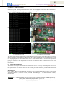
84
Vol 03, Issue 01; January-April 2012
http://technicaljournals.org
International Journal of VLSI and Embedded Systems-IJVES
ISSN: 2249 – 6556
PERIPHERAL I/O DEVICE CONTROL USING MICRO
BLAZE PROCESSOR
B. MURALI KRISHNA1, B. RAGHU KANTH1, K.GNANA DEEPIKA1, V.G. SANTHI
SWAROOP1, T. V. RAMA KRISHNA1, G.PHANI KUMAR2
1
Department of ECE, K.L.University, Vijayawada, AP, India.
2
Assistant Professor, S.V.E.C, Bobbili, AP, India.
ABSTRACT
Embedded Development Kit (EDK) tools are used for this purpose to enables a design of a complete embedded
processor system for implementation in a Xilinx FPGA device. The Micro Blaze embedded soft core processor
is a reduced instruction set computer (RISC) optimized for implementation in Xilinx Field Programmable Gate
Arrays. In this paper the authors presented the controlling of the peripherals like LED`s, push buttons and seven
segment display through UART Communication. Universal Asynchronous Receiver Transmitter (UART) Lite
Interface connects to the PLB (Processor Local Bus) and provides the controller interface for asynchronous
serial data transfer.
Keywords: PLB, EDK, UART, FPGA, LED`s, push buttons.
1. INTRODUCTION
The microprocessors available for use in Xilinx Field Programmable Gate Arrays (FPGAs) with Xilinx EDK
software tools can be broken down into two broad categories. There are soft-core microprocessors (Micro
Blaze) and the hard-core embedded microprocessor (PowerPC). The Micro Blaze is a virtual microprocessor
that is built by combining blocks of code called cores inside a Xilinx Field Programmable Gate Array (FPGA).
The beauty to this approach is that you only end up with as much microprocessor as you need. FPGA contains
programmable logic components called logic blocks and a hierarchy of reconfigurable interconnects that allow
the blocks to be wired together. Logic blocks can be configured to perform complex combinational functions or
merely simple logic gates like AND and XOR. In most of the FPGA`s the logic blocks also include memory
elements which may be simple flip flops or more complete blocks of memory. You can also tailor the project to
your specific needs like Flash, UART, General Purpose Input/output pheriphals and etc.
By using the serial communication we are going to monitor the output of the peripherals like Seven Segment
Display, LED`s, Dip Switches, push buttons which are present on the Diligent Nexys Board. Micro Blaze EDK
has numerous IP cores that give designers pre-made modules through user friendly software. The Nexys2 board
includes several input devices, output devices, and data ports, allowing many designs to be implemented without
the need for any other components. Four pushbuttons and eight slide switches are provided for circuit inputs.
Pushbutton inputs are normally low, and they are driven high only when the pushbutton is pressed. Slide
switches generate constant high or low inputs depending on their position. Pushbutton and slide switch inputs
use a series resistor for protection against short circuits. The outputs will be observed on the putty terminal with
the commands through given through UART communication.
2. UART COMMUNICATION
A universal asynchronous receiver transmitter (UART) is basically a parallel to serial data transmitter and a
serial to parallel data receiver. The asynchronous part refers to the fact that the clock for the UART does not
have to be synchronized to either the transmitting or receiving systems‟ clocks. A modem is composed of two
basic parts, the UART and the analog modulator-demodulator, which is where the term (MoDem) comes from.
During transmission of data the UART is responsible for taking the data from the host machine and turning it
into a serial bit stream that can be sent by the modem over the phone line. During reception of data the UART
takes the serial data from the modem and converts it into parallel data that can be used by the host machine.
Standard UARTs transmit and receive data in 11-bit packets, of which 8-bits are for the data, there is one bit at
the beginning of the packet called the Start bit, which is always a logic 0, and 2 bits at the end called the Stop
bits, which are always a logic 1.
As a Receiver
The two basic parts of the UART receiver are a bit-sampling clock, which runs at least 16 times faster than the
bit rate, and a bit counter. The idle state of the transmission line is at a logic high level. When data is being sent
the transmission line drops because of the start bit. The UART senses this change and counts off 8 increments of
the bit-sampling clock to find the middle of the start bit (assuming this clock is running 16 times faster than the
bit-rate). Then the bit-sampling clock is reset and every time the bit-sampling clock reaches a count of 16 the
transmission line is sampled and the bit counter is incremented. When all eight bits have been collected, the
UART looks for the stop bits and then sends the data to the host machine.
2011 - TECHNICALJOURNALS®, Peer Reviewed International Journals-IJCEA, IJESR, RJCSE, PAPER, ERL, IRJMWC, IRJSP,
IJEEAR, IJCEAR, IJMEAR, ICEAR, IJVES, IJGET, IJBEST – TJ-PBPC, India;
Indexing in Process - EMBASE, EmCARE, Electronics & Communication Abstracts, SCIRUS, SPARC, GOOGLE Database, EBSCO, NewJour, Worldcat,
DOAJ, and other major databases etc.,
85
Vol 03, Issue 01; January-April 2012
http://technicaljournals.org
International Journal of VLSI and Embedded Systems-IJVES
ISSN: 2249 – 6556
Fig 1. UART communication as reciever.
As a Transmitter
The UART Transmitter is composed of three basic parts.
1) A parallel-load shift register,
2) A transmission line flip-flop, and
3) Logic that generates a “register-empty” flag.
Data is loaded in parallel fashion into the shift register, and then shifted out serially to the Line flip-flop, which
holds the transmitted data for one clock cycle. Remember you must also append the Start and Stop bits to the
data in the shift register. As a bit leaves the shift register, 0‟s are shifted into the “empty” slots of the shiftregister. The flag logic should detect when the shift register has all zeros (i.e. the Stop bits have left the shift
register), and set a flag that the transmission is complete. Upon completion of a successful transmission, the
shift register should then load in the next byte of data.
3. EXPERIMENTAL SET UP
In this paper the authors had implemented the experimental set up on Diligent Nexys2 board, which consider of
the required peripherals for the evaluation of the paper. The detail explanation of each peripheral is as follows.
Seven segment display
The Nexys2 board contains a four-digit common anode seven-segment LED display. Each of the four digits is
composed of seven segments arranged in a “figure 8” pattern, with an LED embedded in each segment. Segment
LEDs can be individually illuminated, so any one of 128 patterns can be displayed on a digit by illuminating
certain LED segments and leaving the others dark. Of these 128 possible patterns, the ten corresponding to the
decimal digits are the most useful. The anodes of the seven LEDs forming each digit are tied together into one
“common anode” circuit node, but the LED cathodes remain separate. The common anode signals are available
as four “digit enable” input signals to the 4-digit display.
Fig 2. Digilent nexys2 Seven segment Display.
A scanning display controller circuit can be used to show a four-digit number on this display. This circuit drives
the anode signals and corresponding cathode patterns of each digit in a repeating, continuous succession, at an
update rate that is faster than the human eye can detect.
LED`s
The Nexys2 board includes several input devices, output devices, and data ports, allowing many designs to be
implemented without the need for any other components. Eight LEDs are provided for circuit outputs. LED
anodes are driven from the FPGA via 390-ohm resistors, so a logic „1‟ output will illuminate them with 3-4ma
of drive current. A ninth LED is provided as a power-on LED, and a tenth LED indicates FPGA programming
status.
Push Buttons
Four pushbuttons and eight slide switches are provided for circuit inputs. Pushbutton inputs are normally low,
and they are driven high only when the pushbutton is pressed. Slide switches generate constant high or low
inputs depending on their position. Pushbutton and slide switch inputs use a series resistor for protection against
short circuits and a short circuit would occur if an FPGA pin assigned to a pushbutton or slide switch was
inadvertently defined as an output.
Fig 3. Diligent Nexys2 I/O devices.
2011 - TECHNICALJOURNALS®, Peer Reviewed International Journals-IJCEA, IJESR, RJCSE, PAPER, ERL, IRJMWC, IRJSP,
IJEEAR, IJCEAR, IJMEAR, ICEAR, IJVES, IJGET, IJBEST – TJ-PBPC, India;
Indexing in Process - EMBASE, EmCARE, Electronics & Communication Abstracts, SCIRUS, SPARC, GOOGLE Database, EBSCO, NewJour, Worldcat,
DOAJ, and other major databases etc.,
86
Vol 03, Issue 01; January-April 2012
http://technicaljournals.org
International Journal of VLSI and Embedded Systems-IJVES
ISSN: 2249 – 6556
4. RESULTS AND DISCUSSION
The outputs are obtained by giving he commands to the respective peripharals and checking the out put on the
digilent nexys board. For the given commands the outout will be displayed based on the UART Communication.
The following figures shows the output of the peripharl controlling by the UART communication. By using the
XIlnix10.1 EDK tool the following results are obtianed.
Fig 4. Commands to seven segment Display unit
Fig 6 status of Push buttons
Fig 5. Out put on Nexys board with respect to command.
Fig 7 output of pushbuttons while led`s on
Fig 8 Commands to LEds
Fig 9 Out puts on nexys board.
5. CONCLUSION
The objective was achieved by designing an embedded based project on EDK using Micro Blaze as a processor
where the operations are performed by the processor and developed on XILINX 10.1 and implementing the code
in C language. By this we can conclude that by using a serial communication we can control the Input/output
peripherals which will be having applications like controlling the traffic lights etc. The out puts are verified by
giving the commands in the putty terminal and we can see the output status of each peripheral on the same
terminal also.
6. ACKNOWLEDGMENTS
The authors like to express their thanks to the management of K L University and the department of ECE for
their encouragement and support during this work. Further, the authors would like to acknowledge the head of
the department Dr. Habibbulah Khan for his tremendous support for this research paper.
REFERENCES
[1] A Platform Based on Reconfigurable Architectures and Virtual Instrumentation Applied to the Driving
Automobile Problem. By Anderson Correia, Carlos H. Llanos, Rodrigo W. Carvalho and Sadek A. Alfaro,
February 2007.
2011 - TECHNICALJOURNALS®, Peer Reviewed International Journals-IJCEA, IJESR, RJCSE, PAPER, ERL, IRJMWC, IRJSP,
IJEEAR, IJCEAR, IJMEAR, ICEAR, IJVES, IJGET, IJBEST – TJ-PBPC, India;
Indexing in Process - EMBASE, EmCARE, Electronics & Communication Abstracts, SCIRUS, SPARC, GOOGLE Database, EBSCO, NewJour, Worldcat,
DOAJ, and other major databases etc.,
87
Vol 03, Issue 01; January-April 2012
http://technicaljournals.org
International Journal of VLSI and Embedded Systems-IJVES
ISSN: 2249 – 6556
[2] Designing A Simple Character Generator As A Peripheral For Microblaze(TM) by DRI technologies
version1 in 2005.
[3] Micro Blaze Tutorial Creating a Simple Embedded System and Adding Custom Peripherals Using Xilinx
EDK Software Tools by Rod Jesman Fernando Martinez Vallina Jafar Saniie for Illinois institute of technology.
[4] Xilinx Micro Blaze User guide.
[5] Diligent nexys2 user manual guide for I/O peripherals.
[6] Spartan 3E FPGA user manual guide for I/O peripherals.
[7] www. Wikipidea.org
[8] www.Xilinx.com
[9] Design and Implementation of Area-optimized AES Based on FPGA by AI-WEN LUO, QING-MING YI,
MIN SHI in IEEE 2011.
[10] Design and Simulation of UART Serial Communication Module Based on VHDL by FANG Yi-yuan and
CHEN Xue-jun in IEEE 2011.
[11] FPGA Implementation of RS232 to Universal serial bus converter at 2011 IEEE Symposium on Computers
& Informatics by V.Vijaya, Rama Valupadasu, B.Rama Rao Chunduri, Ch.Kranthi Rekha, B.Sreedevi.
[12] High-Throughput, Lossless Data Compression on FPGAs in IEEE International Symposium on FieldProgrammable Custom Computing Machines by Bharat Sukhwani , Bulent Abali, Bernard Brezzo, Sameh
Asaad.
Authors Biography:
B.Muralikrishna was born in AP, India. He received his, Diploma degree in Electronics &
Communication Engineering from SIR C.R.Reddy Polytechnic, Eluru, A.P., Affiliated to the
SBTE &T in 2004, B.Tech degree in Electronics & Communications Engineering from Nimra
College of Engineering & Technology, Vijayawada, A.P., India, Affiliated to the JNTU
Hyderabad in 2007, M.Tech degree in VLSI Design from GITAM University Vishakhapatnam,
A.P India, in 2010. Presently he is working as Assistant Professor, Department of ECEin
K.L.University, Guntur, AP, India. He had one year experience in Viraj IT solutions PVT Ltd. as Software
Engineer during 2007-2008. He had worked as Teaching Assistant in GITAM University, Vishakhapatnam
during 2009-2010, Where he has been engaged in the teaching, research and development of Low-Power VLSI,
Design for Testability, CPLD‟s & FPGA Architectures, Embedded Systems and Fault Tolerance.
B. Raghu Kanth was born at Vijayawada Andhra Pradesh. He obtained his Bachelor`s degree
from JNTU, HYD in ECE Department in 2007. He is pursuing M.Tech in VLSI from
K.L.University at Vijayawada. He has more than two and half years of teaching experience and
having four International Journal publishing. His area of interest is in Analog VLSI, Low-power
VLSI and Testing.
G Santhi Swaroop Vemana was born in A.P, India. He received B.TECH degree in Electronics
and Communication Engineering from Jawaharlal Nehru technological university in 2008. He
worked as OFC engineer at united telecom‟s ltd at GOA during 2009-2010. Presently he is
pursuing M.Tech VLSI Design in KL University. His research interests include FPGA
Implementation, Low Power Design.
Dr. T. Venkata Rama Krishna was on August 12, 1972. He received B. Tech from Nagrajuna
University, in 1997 and M.E from PSG College of Technology, in 2000, respectively, all in
Electronics and Communication Engineering. He received the Ph.D degree from JNTU,
Kakinada in 2011. His current research interests include Antenna Measurement Techniques
applied to Compact Antenna Test Ranges, Communication Systems. He has published several
papers in National and International Journals and presented papers at National/International
conferences. He is the Life Member of IETE and ISTE.
G. Phani Kumar was born on 26th October at Kakinada. He obtained his Bachelor‟s degree
from JNTU, HYD in ECE Department in 2007. He obtained his M.Tech from SATYABHAMA
University, Chennai in 2009. He is currently working as an assistant professor in S.V.
Engineering College at Bobbili from 2009. He is having two and half years of teaching
experience. His area of interest is in Analog VLSI, Low power and testing.
2011 - TECHNICALJOURNALS®, Peer Reviewed International Journals-IJCEA, IJESR, RJCSE, PAPER, ERL, IRJMWC, IRJSP,
IJEEAR, IJCEAR, IJMEAR, ICEAR, IJVES, IJGET, IJBEST – TJ-PBPC, India;
Indexing in Process - EMBASE, EmCARE, Electronics & Communication Abstracts, SCIRUS, SPARC, GOOGLE Database, EBSCO, NewJour, Worldcat,
DOAJ, and other major databases etc.,