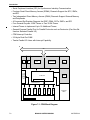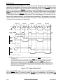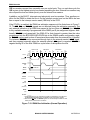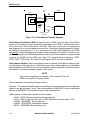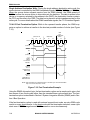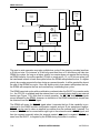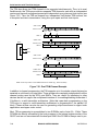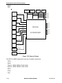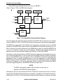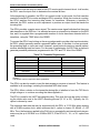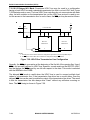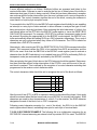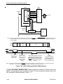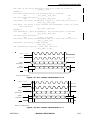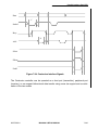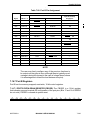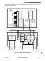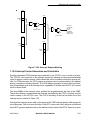
1
SECTION 7
COMMUNICATION PROCESSOR MODULE (CPM)
INTRODUCTION
The CPM includes many blocks that work together to allow an extremely flexible and integrated approach to solving many communications problems. The CPM (see Figure 7-1) includes the following modules:
• RISC Controller
• Four Full-Duplex Serial Communication Controllers (SCCs) Support the Following Protocols:
—IEEE 802.3/Ethernet (Optional Feature on SCC)
—High-Level/Synchronous Data Link Control (HDLC/SDLC)
—HDLC Bus (Multidrop Bus Configuration of HDLC)
—AppleTalk (HDLC-Based Local Area Network (LAN) Protocol)
—Universal Asynchronous Receiver Transmitter (UART)
—Synchronous UART (Isochronous, 1x Clock Mode)
—Binary Synchronous Communication (BISYNC)
—Totally Transparent Operation
—Signaling System #7 (HDLC-Based Protocol. RAM Microcode Option Only)
— Profibus (RAM Microcode Option Only)
—Asynchronous HDLC (RAM Microcode Option Only)
—Multiple Chanel GCI (RAM Microcode Option Only)
—ATM Framing (RAM Microcode Option Only)
—Enhanced Ethernet Filtering (RAM Microcode Option Only)
• Four Independent Baud Rate Generators
• Two Serial Management Controllers (SMCs) Provide Additional UART and Totally
Transparent Functionality or Support the GCI Channel 0 and 1 Monitor and C/I Channels in Integrated Services Digital Network (ISDN)
• Serial Interface Provides Nonmultiplexed Serial Interface (NMSI) for the Four SCCs (includes TXD, RXD, TCLK, RCLK, RTS, CTS, and CD pins)
• Time Slot Assigner (TSA) Supports Multiplexing of Data from any of the Four SCCs and
Two SMCs onto Two Time-Division Multiplexed (TDM) Interfaces. The TSA Supports
the Following TDM Formats:
—T1/CEPT Lines
—Pulse Code Modulation (PCM) Highway Interface
—ISDN Primary Rate
—Motorola Interchip Digital Link (IDL)
—General Circuit Interface (GCI), also known as IOM-2
—User-Defined Interfaces
MOTOROLA
MC68360 USER’S MANUAL
7-1
Introduction
• Serial Peripheral Interface (SPI) for Synchronous Interchip Communication
• Fourteen Serial Direct Memory Access (SDMA) Channels Support the SCC, SMCs,
and SPI
• Two Independent Direct Memory Access (IDMA) Channels Support External Memory
and Peripherals
• A Command Set Register Supports the RISC, IDMA, SCCs, SMCs, and SPI
• Four General-Purpose 16-Bit Timers or Two 32-Bit Timers
• Internal Timers to Implement Up to 16 Additional Timers
• General-Purpose Parallel Port for Parallel Protocols such as Centronics (Can Also Be
Used as Standard Parallel I/O)
• CPM Interrupt Controller
• 2.5-kbyte Dual-Port RAM
• Twelve Parallel I/O Lines with Interrupt Capability
IMB
CPM
PAR
I/O
PARALLEL
INTERFACE
PORT (PIP)
BRG
DUAL-PORT
RAM
INTERRUPT
CONTROLLER
FOUR
TIMERS
TWO
IDMAs
32-BIT RISC
INTERNAL TIMER
SPI
SMC2
SMC1
SCC4
SCC3
SCC2
SCC1
PERIPHERAL BUS
FOURTEEN
SDMAs
SERIAL INTERFACE
TIME SLOT ASSIGNER
NOTE: The term "CP" refers to the nonshaded portion of the CPM.
Figure 7-1. CPM Block Diagram
7-2
MC68360 USER’S MANUAL
MOTOROLA
RISC Controller
7.1 RISC CONTROLLER
The RISC controller is the 32-bit central controller of the communication processor module
(CPM). Since its execution occurs on a separate bus that is hidden from the user, it does
not impact CPU32+ core performance. The RISC controller works with the serial channels
and parallel interface port (PIP) to implement the user-chosen protocols and to manage the
SDMA channels that transfer data between the SCCs and memory. The RISC controller
contains an internal timer that can be used to implement up to 16 additional timers for the
user application software. These features are collectively known as the communication processor (CP), which is a subset of the overall CPM. Additionally, the RISC controller can
manage the operation of the IDMA channels, if desired. The 32-bit RISC handles the lower
layer tasks and DMA control activities, leaving the 32-bit CPU32+ core (or other external
processor) free to handle higher layer activities. Thus, the QUICC can be thought of as a
dual 32-bit processor system.
The RISC controller communicates with the host (CPU32+ core or other external processor)
in several ways. First, many parameters are exchanged through the dual-port RAM. In the
case of simultaneous accesses (at least one of which is a write operation), the RISC controller may be delayed by one clock in its access to the dual-port RAM. The host is never
delayed. Second, the RISC controller can execute special commands issued by the host.
These commands are only required to be issued in special situations. Third, the RISC controller can generate interrupts through the CPM interrupt controller. Fourth, status/event registers, which show events that have occurred within the RISC, may be read at any time by
the CPU32+ or an external processor.
The RISC controller has the ability to control a set of up to 16 timers. These timers are separate and distinct from the four general-purpose timers and baud rate generators in the
CPM. The 16 timers are ideally used in protocols that do not require extreme precision, but
in which it is desirable to off-load the host CPU from having to scan the timer tables that are
created in software. These timers are clocked from an internal timer used only by the RISC
controller.
The RISC controller uses the peripheral bus to communicate with all of its peripherals. Each
SCC has a separate receive and transmit FIFO. The SCC1 FIFOs are 32-bytes each; the
other SCC FIFOs are 16-bytes each. The SMC and SPI FIFO sizes are double-buffered.
The PIP is a single register interface.
The following priority scheme determines the processing priority of the RISC controller. It is
as follows:
1. Reset in CP Command Register or System Reset
2. DMA Bus Error
3. Commands Issued to the CP Command Register
4. CC1 Rx
5. SCC1 Tx
6. SCC2 Rx
7. SCC2 Tx
MOTOROLA
MC68360 USER’S MANUAL
7-3
RISC Controller
8. CC3 Rx
9. SCC3 Tx
10. SCC4 Rx
11. SCC4 Tx
12. SMC1 Rx
13. SMC1 Tx
14. SMC2 Rx
15. SMC2 Tx
16. SPI Rx
17. SPI Tx
18. PIP
19. RISC Timer Tables
The RISC controller has an option to execute microcode from a portion of user RAM, located
in the on-chip dual-port RAM. In this mode, either 512 bytes or 1024 bytes of the user RAM
cannot be accessed by the host or another bus master and are used exclusively by the
RISC. In this mode, the RISC controller can fetch instructions from both the dual-port RAM
and its private ROM. This mode allows Motorola to add new protocols or enhancements to
the QUICC in the form of Motorola-supplied RAM microcodes. The binary microcode is
obtained from Motorola and then loaded by the user into the dual-port RAM.
The RISC controller contains one configuration register described in the following paragraph.
7.1.1 RISC Controller Configuration Register (RCCR)
The 16-bit, memory-mapped, read-write RCCR is used to configure the RISC processor and
controls the RISC internal timer. This register is initialized to zero at reset. Bits 0-7 should
not be modified unless the user is downloading a Motorola-supplied RAM microcode package..
15
TIME
14
—
13
12
11
10
9
8
7
6
TIMEP
5
4
3
RESERVED
2
1
0
TIME—Timer Enable
This bit enables the RISC controller internal timer. The timer will generate a tick to the
RISC based on the value programmed into the TIMEP bit. TIME may be modified at any
time to start or stop the scanning of the RISC timer tables.
Bit 14—Reserved
TIMEP—Timer Period
This field controls the RISC controller timer tick. The RISC timer tables are scanned on
each timer tick. The input to this timer tick generator is the general system clock divided
by 1024. The formula is (TIMEP + 1) × 1024 = (general system clock period). Thus, a val7-4
MC68360 USER’S MANUAL
MOTOROLA
Command Set
ue of 0 stored in these bits gives a timer tick of 1 × (1024) = 1024 general system clocks.
A value of 63 (decimal) stored in these bits gives a timer tick of 64 × (1024) = 65536 general system clocks.
Bits 7-0—Reserved - set to zero.
7.1.2 RISC Microcode Revision Number
The RISC controller writes a revision number stored in its ROM to a dual-port RAM location
called REV_num. REV_num is located in the miscellaneous parameter RAM. The other
locations are reserved for future use. The microcode rivision number only reflect the revision
of the micro code. It dose not always refrect the MASK number.
Address
Name
Width
Description
Misc Base + 00
REV_num
Word
Microcode Revision Number
Misc Base + 02
RES
Word
Reserved
Misc Base + 04
RES
Long
Reserved
Misc Base + 08
RES
Long
Reserved
7.2 COMMAND SET
The host processor (CPU32+ or other external processor) issues commands to the RISC by
writing to the command register (CR). The CR only needs to be accessed on rare occasions.
For instance, to terminate the transmission of a frame by an SCC without waiting until the
end of the frame, a STOP TX command can be issued to an SCC through the command
register. The commands are described in general terms in the following paragraphs; they
are described in specific terms when the protocol or feature is described in detail.
The host should set the FLG bit in the CR when it issues commands. The CP clears FLG
after completing the command to indicate to the host that it is ready for the next command.
Subsequent commands to the CR may be given only after FLG is cleared. The software
reset command (issued by setting the RST bit) may be given regardless of the state of FLG,
but the host should still set FLG when setting RST.
The CR, a 16-bit, memory-mapped, read-write register, is cleared by reset.
15
RST
14
13
—
12
11
10
9
OPCODE
8
7
6
5
CH NUM
4
3
2
—
1
0
FLG
RST—Software Reset Command
This bit is set by the host and cleared by the CP. On execution of this command, the RST
bit and the FLG bit are cleared within two general system clocks. The RISC reset routine
is approximately 60 clocks long, but the user can begin initialization of the CP immediately
after this command is given. This command is useful when the host wants to reset the registers and parameters for all the channels (SCCs, SMCs, SPI, and PIP) as well as the
RISC processor and RISC timer tables. This command does not affect the serial interface
(SI) or the parallel I/O registers.
MOTOROLA
MC68360 USER’S MANUAL
7-5
Command Set
Bits 14–12, 3–1—Reserved
OPCODE—Operation Code
The opcodes are listed in Table 7-1.
Table 7-1. Opcodes
Opcode
SCC
SMC (UART/Trans)
SMC (GCI)
SPI
0000
INIT RX & TX
PARAMS
INIT RX & TX PARAMS
INIT RX & TX
PARAMS
INIT RX & TX
PARAMS
0001
INIT RX
PARAMS
INIT RX PARAMS
INIT RX
PARAMS
0010
INIT TX PARAMS
INIT TX PARAMS
INIT TX PARAMS
0011
ENTER HUNT
MODE
ENTER HUNT MODE
0100
STOP TX1
STOP TX
0101
GR STOP TX2
0110
RESTART TX
RESTART TX
0111
CLOSE RX BD
CLOSE RX BD
1000
SET GROUP
ADDR
Timer
INIT IDMA
CLOSE RX BD
SET TIMER
1001
1010
IDMA
GCI TIMEOUT
RESET BCS
GCI ABORT REQ
1011
1100
U
U
U
U
U
U
1101
U
U
U
U
U
U
1110
U
U
U
U
U
U
1111
U
U
U
U
U
U
NOTES:
1.STOP TX = MC68302 original STOP TRANSMIT command.
2.GR STOP TX = GRACEFUL STOP TRANSMIT command.
INIT TX and RX PARAMETERS. This command initializes the transmit and receive parameters in the parameter RAM to the values that they had after the last reset of the CP.
This command is especially useful when switching protocols on a given serial channel.
INIT RX PARAMETERS. This command initializes the receive parameters of the serial
channel.
INIT TX PARAMETERS. This command initializes the transmit parameters of the serial
channel.
ENTER HUNT MODE. This command causes the receiver to stop receiving and begin
looking for a new frame. The exact operation of this command may vary depending on the
protocol used.
STOP TX. This command aborts the transmission from this channel as soon as the transmit FIFO has been emptied. It should be used in cases where transmission needs to be
stopped as quickly as possible. Transmission will proceed when the RESTART command
is issued.
7-6
MC68360 USER’S MANUAL
MOTOROLA
Command Set
GRACEFUL STOP TX. This command stops the transmission from this channel as soon
as the current frame has been fully transmitted from the transmit FIFO. Transmission will
proceed once the RESTART command is issued and the R-bit is set in the next transmit
buffer descriptor.
RESTART TX. When the STOP TX command has been issued, this command can be
used to restart the transmission at the current buffer descriptor.
CLOSE RX BD. This command causes the receiver to simply close the current receive
buffer descriptor, making the receive buffer immediately available for manipulation by the
user. Reception continues normally using the next available buffer descriptor. This command may be used to access the data buffer without waiting until the data buffer is completely filled by the SCCµSET TIMER. This command activates, deactivates, or
reconfigures one of the 16 timers in the RISC timer table.
SET GROUP ADDRESS. This command sets a bit in the hash table for the Ethernet logical group address recognition function.
GCI ABORT REQUEST. The GCI receiver sends an abort request on the E-bit.
GCI TIMEOUT. The GCI performs the timeout function.
RESET BCS. This command is used in BISYNC mode to reset the block check sequence
calculation.
Undefined (U). Reserved for use by Motorola-supplied RAM microcodes.
CH NUM—Channel Number
These bits are set by the host to define the specific sub-block on which the command is
to operate. Some sub-blocks share channel number encodings if their commands are mutually exclusive.
0000 SCC1
0001
0010
0011
0100 SCC2
0101 SPI/RISC Timers
0110
0111
1000 SCC3
1001 SMC1/IDMA1
1010
1011
1100 SCC4
1101 SMC2/IDMA2
1110
1111
FLG—Command Semaphore Flag
The bit is set by the host and cleared by the CP.
MOTOROLA
MC68360 USER’S MANUAL
7-7
Dual-Port RAM
0 = The CP is ready to receive a new command.
1 = The CR contains a command that the CP is currently processing. The CP clears
this bit at the end of the command execution or after reset.
7.2.1 Command Register Examples
To perform a complete reset of the CP, the value $8001 should be written to the CR. Following this command, the CR will return the value $0000 in two clocks.
To execute an ENTER HUNT MODE command to SCC3, the value $0381 should be written
to the CR. While the command is executing, the CR will return the value $0381. When the
command has been completely executed, the CR will return the value $0380.
7.2.2 Command Execution Latency
The worst-case command execution latency is 120 clocks. The typical command execution
latency is about 40 clocks.
7.3 DUAL-PORT RAM
The CPM has 2560 bytes of static RAM configured as dual-port memory. The dual-port RAM
memory map is shown in Figure 7-2, and a block diagram is shown in Figure 7-3.
0
TOTAL 2560 BYTES
BDs/DATA/UCODE—512 BYTES
MBAR POINTS
TO THE BASE
0.5K
BDs/DATA/UCODE—512 BYTES
1K
BDs/DATA—512 BYTES
1.5K
BDs/DATA/UCODE—256 BYTES
2K
2.5K
3K
PARAMETER RAM—768 BYTES
3.5K
BDs/DATA IN ANY UNUSED SPACE
4K
Figure 7-2. Dual-Port RAM Memory Map
7-8
MC68360 USER’S MANUAL
MOTOROLA
Dual-Port RAM
SYSTEM
RAM
1792 BYTES
512
BYTES
ADDRESS
SELECTOR
CP MICROCODE
ADDRESS
512
BYTES
CP MICROCODE DATA
512
BYTES
256
BYTES
PERIPHERAL
DATA BUS
IMB
ADDRESS
BUS
ADDRESS
SELECTOR
INTERNAL
PERIPHERAL
ADDRESS
PARMETER
RAM
768 BYTES
IMB
DATA BUS
Figure 7-3. Dual-Port RAM Block Diagram
The dual-port RAM can be accessed by the RISC or one of four bus masters: CPU32+ core,
IDMAs, SDMAs, or external bus master. When the dual-port RAM is accessed by an external bus master, CPU32+ core, IDMA, or SDMA channel, it is accessed in three clocks. When
the dual-port RAM is accessed by the RISC, it is accessed in one clock. In the case of simultaneous access (with at least one write operation), the RISC is delayed by one clock.
When the dual-port RAM is accessed by the CPU32+ core, IDMAs, SDMAs, or external bus
master, the data and address are taken from the IMB. The data is then presented on the IMB
data bus. The RISC has access to the entire dual-port RAM for data fetches and portions of
the system RAM for microcode instruction fetches.
The dual-port RAM is used for five possible tasks; any two tasks can occur simultaneously.
The first use is to store parameters associated with the SCCs, SMCs, SPI, and IDMAs in the
768-byte parameter RAM. The second use is to store the buffer descriptors that describe
where data is to be received and transmitted from. The third use is to store data from the
serial channels. This usage is optional since data may also be stored externally in the system memory. The fourth use is to store RAM microcode for the RISC processor. This feature
allows additional protocols to be added by Motorola in the future. The fifth use is for additional scratchpad RAM space for the user program.
MOTOROLA
MC68360 USER’S MANUAL
7-9
Dual-Port RAM
Only the parameters in the parameter RAM and the microcode RAM option require fixed
addresses to be used. The buffer descriptors, buffer data, and scratchpad RAM may be
located in the internal system RAM or in any unused parameter RAM (for instance, in the
available area when a serial channel or sub-block is not being used).
When a microcode from RAM is executed, certain portions of the system RAM are no longer
available. This includes either the first 512-byte block and the last 256-byte block for a small
RAM microcode, and the first two 512-byte blocks and the last 256-byte block for a large
RAM microcode. The third 512-byte block is always available as system RAM.
7.3.1 Buffer Descriptors
The SCCs, SMCs, SPI always use buffer descriptors for controlling data buffers. The buffer
descriptor format of the SCCs, SMCs, and SPI is identical. The buffer descriptor format for
these channels is shown in the following illustration.
150
OFFSET + 0
STATUS AND CONTROL
OFFSET + 2
DATA LENGTH
OFFSET + 4
HIGH-ORDER DATA BUFFER POINTER
OFFSET + 6
LOW-ORDER DATA BUFFER POINTER
If the IDMA is used in the buffer chaining or auto buffer mode, the IDMA channel also uses
buffer descriptors. The buffer descriptors for the IDMA are described in 7.6.1 IDMA Key Features;.
7.3.2 Parameter RAM
The CP maintains a section of dual-port RAM called the parameter RAM. This RAM contains
many parameters for the operation of the SCCs, SMCs, SPI, and the IDMA channels. An
overview of the parameter RAM structure is shown in Figure 7-4. The exact definition of the
parameter RAM is contained in each subsection describing a device that uses a parameter
RAM.
7-10
MC68360 USER’S MANUAL
MOTOROLA
RISC Timer Tables
3k
TOTAL 768 BYTES
SCC1/MISC
192 BYTES
SCC2/SPI
192 BYTES
256 BYTES/PAGE
SCC3/SMC1/IDMA1
192 BYTES
SCC4/SMC2/IDMA2
192 BYTES
4k
Figure 7-4. Parameter RAM Overview
7.4 RISC TIMER TABLES
The RISC controller has the ability to control up to 16 timers. These timers are separate from
the four general-purpose timers and baud rate generators in the CPM. The 16 timers are
ideally used in protocols that do not require extreme precision, but in which it is desirable to
off-load the host CPU from having to scan the timer tables that are created in software.
These timers are clocked from an internal timer used only by the RISC.
The features of the RISC timer tables are as follows:
• Up to 16 Timers Supported
• Two Timer Modes: One-Shot and Restart
• Maskable Interrupt on Timer Expiration
• Programmable Timer Resolution As Low As 41 µs at 25 MHz
• Maximum Timeout Period of 172 Sec at 25 MHz
MOTOROLA
MC68360 USER’S MANUAL
7-11
RISC Timer Tables
• Continuously Updated Reference Counter
All operations on the RISC timer tables are based on a fundamental "tick" of the RISC internal timer, which is programmed in the RISC RCCR. The tick is a multiple of 1024 general
system clocks. (See 7.1 RISC Controller for more details.)
The RISC timer tables have the lowest priority of all RISC operations. Therefore, if the RISC
is so busy with other tasks that it does not have time to service the timer during a tick interval,
one or more of the timers may not be updated during a tick.
This behavior can actually be used to estimate the worst-case loading of the RISC processor. (See Table 7-2 for more details.)
The RISC timer tables are configured in the RCCR, the RISC timer table parameter RAM,
and by the SET TIMER command issued to the CP command register, the RISC timer event
register, and the RISC timer mask register.
7.4.1 RISC Timer Table Parameter RAM
Two areas of internal RAM are used for the RISC timer tables: the RISC timer table parameter RAM and RISC timer table entries (see Figure 7-5). The RISC timer table parameter
RAM area begins at the RISC timer base address (see Table 7-2). This area is used for the
general timer parameters.
INTERNAL DUAL-PORT RAM
CAN BE ANYWHERE IN
THE DUAL-PORT RAM
16 RISC
TIMER
TABLE
ENTRIES
(UP TO 64 BYTES)
POINTER
TM_BASE
ALWAYS THE SAME LOCATION
IN PARAMETER RAM
RISC
TIMER
TABLE
PARAMETER
RAM
(14 BYTES)
Figure 7-5. RISC Timer Table RAM Usage
7-12
MC68360 USER’S MANUAL
MOTOROLA
RISC Timer Tables
Table 7-2. RISC Timer Table Parameter RAM
Address
Name
Width
Description
Timer Base + 00
TM_BASE
Word
RISC Timer Table Base Address
Timer Base + 02
TM_ptr
Word
RISC Timer Table Pointer
Timer Base + 04
R_TMR
Word
RISC Timer Mode Register
Timer Base + 06
R_TMV
Word
RISC Timer Valid Register
Timer Base + 08
TM_cmd
Long
RISC Timer Command Register
Timer Base + 0C
TM_cnt
Long
RISC Timer Internal Count
NOTE: Boldfaced items are initialized by the user.
TM_BASE. The actual RISC timers are located by the user as a small block of memory in
the dual-port RAM. TM_BASE is the offset from the beginning of dual-port RAM where that
block resides. The user should allocate 4 bytes at TM_BASE for each timer used (64 bytes
at TM_BASE if all 16 timers are used). If less than 16 timers are used, the timers should
always be allocated in ascending order (RISC timer 0, RISC timer 1, etc.) to save space. For
example, if the user only needs two timers, then 8 bytes are required at location TM_BASE
as long as the user only enables RISC timer 0 and RISC timer 1.
NOTE
TM_BASE should always be aligned to a long-word boundary
(i.e., evenly divisible by 4).
TM_ptr. This value is used exclusively by the RISC to point to the next timer to be accessed
in the timer table. It should not be modified by the user.
R_TMR. This value is used exclusively by the RISC to store the mode of the timer: one-shot
(bit is zero) or restart (bit is one). R_TMR should not be modified by the user. The SET
TIMER command should be used instead.
R_TMV. This value is used exclusively by the RISC to store whether a timer is currently
enabled. A bit is a one if the corresponding timer is enabled. R_TMV should not be modified
by the user. The SET TIMER command should be used instead.
TM_cmd. This value is used as a parameter location when the SET TIMER command is
issued. The user should write this location prior to issuing the SET TIMER command. This
parameter is defined as follows:
31
30
V
R
29
20
—
19
16
TIMER NUMBER
15
0
TIMER PERIOD (16 BITS)
V—Valid
This bit should be set to enable the timer and cleared to disable the timer.
R—Restart
This bit should be set for an automatic restart or cleared for a one-shot operation of the
timer.
MOTOROLA
MC68360 USER’S MANUAL
7-13
RISC Timer Tables
Bits 29–20—Reserved
These bits should be written with zeros.
Bits 19–16—Timer Number
The timer number is a value from 0 to 15 that signifies the timer is configured.
Bits 15–0—Timer Period
The timer period is the 16-bit timeout value of the timer. The maximum value is 65536,
which is programmed by writing $0000 to the timer period.
TM_cnt. This value is simply a tick counter that is updated by the RISC after each tick. It is
updated if the RISC internal timer is enabled, regardless of whether any of the 16 timers are
enabled. It can be used to track the number of ticks that the RISC has received and
responded to. This value is updated only after the RISC scans the timer table.
7.4.2 RISC Timer Table Entries
The actual 16 timers themselves are located in the block of memory following the TM_BASE
location. Each timer occupies 4 bytes. The first word forms the initial value of the timer written during the execution of the SET TIMER command, and the next word is the current value
of the timer, which is decremented until it reaches zero. These locations should not be modified by the user; they are documented only as a debugging aid for user code.
7.4.3 RISC Timer Event Register (RTER)
This 16-bit register is used to report events recognized by the 16 timers and to generate
interrupts. Bit 0 corresponds to timer 0, and bit 15 corresponds to timer 15. Note that an
interrupt will only be generated if the RISC timer table bit is set in the CPM interrupt mask
register. RTER may be read at any time. A bit is cleared by writing a one (writing a zero does
not affect a bit’s value), and more than one bit may be cleared at a time. This register is
cleared at reset.
7.4.4 RISC Timer Mask Register (RTMR)
This 16-bit register is used to enable interrupts that may be generated in the RISC timer
event register. If a bit is set, it enables the corresponding interrupt in the RTER. If a bit is
cleared, it masks the corresponding interrupt in the RTER. Note that an interrupt will only be
generated if the RISC timer table bit is set in the CPM interrupt mask register. This readwrite register is cleared at reset.
7.4.5 SET TIMER Command
This command is used to enable, disable, and configure the 16 timers in the RISC timer table. The SET TIMER command is issued to the CR. This means the value $0851 should be
written to CR. However, before writing this value, the TM_cmd value should be set up by the user. See 7.4.1
RISC Timer Table Parameter RAM for details.
7.4.6 RISC Timer Initialization Sequence
The following sequence initializes the RISC timers:
1. Configure the RCCR to determine the desired tick interval that will be used for the en-
7-14
MC68360 USER’S MANUAL
MOTOROLA
RISC Timer Tables
tire timer table. The TIME bit would normally be turned on at this time; however, it can
be turned on later if it is required that all RISC timers be synchronized.
2. Determine the maximum number of timers to be located in the timer table and configure TM_BASE in the RISC timer table parameter RAM to point to a location in the dual
port RAM with 4 × N bytes available, where N is the number of timers. If N is less than
16, use timer 0 through timer N–1 (for space efficiency).
3. Clear the TM_cnt in the RISC timer table parameter RAM to show how many ticks
have elapsed since the RISC internal timer was enabled. This step is optional.
4. Clear the RISC timer event register if it is not already cleared. (Ones are written to
clear this register.)
5. Configure the RTMR to enable those timers that should generate interrupts. (Ones enable interrupts.)
6. Set the RISC timer table bit in the CPM interrupt mask register to generate interrupts
to the system. (The CPM interrupt controller may require other initialization not mentioned here.)
7. Configure the TM_cmd field of the RISC timer table parameter RAM. At this point, determine whether a timer is to be enabled or disabled, one-shot or restart, and what its
timeout period should be. If the timer is being disabled, the parameters (other than the
timer number) are ignored.
8. Issue the SET TIMER command by writing $0861 to the CR.
9. Repeat the preceding two steps for each timer to be enabled or disabled.
7.4.7 RISC Timer Initialization Example
The following sequence initializes RISC timer 0 to generate an interrupt approximately every
second using a 25-MHz general system clock:
1. Write the TIMEP bits of the RCCR with 111111 to generate the slowest clock. This value will generate a tick every 65536 clocks, which is every 2.6 ms at 25 MHz.
2. Configure TM_BASE in the RISC timer table parameter RAM to point to a location in
the dual-port RAM with 4 bytes available. Assuming the beginning of dual-port RAM is
available, write $0000 to TM_BASE.
3. Write $0000 to TM_cnt in the RISC timer table parameter RAM to see how many ticks
have elapsed since the RISC internal timer was enabled. This step is optional.
4. Write $FFFF to the RTER to clear any previous events.
5. Write $0001 to the RTMR to enable RISC timer 0 to generate an interrupt.
6. Write $00020000 to the CPM interrupt mask register to allow the RISC timers to generate a system interrupt. Initialize the CPM interrupt configuration register.
7. Write $C0000EE6 to the TM_cmd field of the RISC timer table parameter RAM. This
enables RISC timer 0 to time out after 3814 (decimal) ticks of the timer. The timer will
automatically restart after it times out.
8. Write $0851 to the CR to issue the SET TIMER command.
9. Set the TIME bit in the RCCR to enable the RISC timer to begin operation.
MOTOROLA
MC68360 USER’S MANUAL
7-15
RISC Timer Tables
7.4.8 RISC Timer Interrupt Handling
The following sequence describes what would normally occur within an interrupt handler for
the RISC timer tables:
1. Once an interrupt occurs, read the RISC timer event register to see which timer or timers have caused interrupts. The RISC timer event bits would normally be cleared at
this time.
2. Issue additional SET TIMER commands at this time or later, as desired. Nothing need
be done if the timer is being restarted automatically for a repetitive interrupt.
3. Clear the R-TT bit in the CPM interrupt status register.
4. Execute the RTE instruction.
7.4.9 RISC Timer Table Algorithm
The RISC scans the timer table once every tick. For each valid timer in the timer table, the
RISC decrements the count and checks for a timeout. If no timeout occurs, it moves to the
next timer. If a timeout occurs, the RISC sets the corresponding event bit in the RISC timer
event register. It checks to see if the timer is to be restarted. If so, it leaves the timer valid
bit set in the R_TMV location and resets the current count to the initial count; otherwise, it
clears the R_TMV bit. Once the timer table is scanned, the RISC updates the TM_cnt value
in the RISC timer table parameter RAM and ceases working on the timer tables until the next
tick.
If a SET TIMER command is issued, the RISC controller makes the appropriate modifications to the timer table and parameter RAM, but does not scan the timer table until the next
tick of the internal timer. It is important to use the SET TIMER command to properly synchronize the timer table alterations to the execution of the RISC.
7.4.10 RISC Timer Table Application: Track the RISC Loading
The RISC timers can be used to track the loading of the RISC controller. The following
sequence gives a method for using the 16 RISC timers to determine if the RISC controller
ever exceeds the 96% utilization level during any tick interval. Removing the timers then
adds a 4% margin to the RISC utilization level. The aggressive user can use this technique
to push the RISC performance to its limit in an application.
The user should use the standard initialization sequence, with the following differences:
1. Program the tick of the RISC timers to be 1024 x 16 = 16384.
2. Disable RISC timer interrupts, if desired.
3. Using the SET TIMER command, initialize all 16 RISC timers to have a timer period of
$0000, which equates to 65536.
4. Program one of the four general-purpose timers to increment once every tick. The general-purpose timer should be free-running and should have a timeout of 65536.
5. After hours of operation, compare the general-purpose timer to the current count of
RISC timer 15. If RISC timer 15 is more than two ticks different from the general-purpose timer, the RISC controller has, during some tick interval, exceeded the 96% uti-
7-16
MC68360 USER’S MANUAL
MOTOROLA
Timers
lization level.
NOTE
The general-purpose timers are up-counters, but the RISC timers are down-counters. The user should consider this fact when
comparing timer counts.
7.5 TIMERS
The CPM includes four identical, 16-bit, general-purpose timers or two 32-bit timers. Each
general-purpose timer consists of a timer mode register (TMR), a timer capture register
(TCR), a timer counter (TCN), a timer reference register (TRR), and a timer event register
(TER). The TMR contains the prescaler value programmed by the user. In addition, there is
one timer global configuration register (TGCR). The timer block diagram is shown in Figure
7-6.
TGCR
GLOBAL CONFIGURATION REGISTER
TER1
TMR1
EVENT REGISTER
GENERAL
SYSTEM
CLOCK
TIMER
CLOCK
GENERATOR
MODE REGISTER
PRESCALER
MODE BITS
DIVIDER
TGATE1
TGATE2
TIN1
TIN2
TIN3
CLOCK
TIN4
TCN1
TIMER COUNTER
TRR1
REFERENCE REGISTER
CAPTURE
DETECTION
TOUT1
TOUT2
TCR1
CAPTURE REGISTER
TOUT3
TOUT4
TIMER1
TIMER2
TIMER3
TIMER4
Figure 7-6. Timer Block Diagram
7.5.1 Timer Key Features
The four identical general-purpose timers have the following features:
• Maximum Period of 10.7 Sec (at 25 MHz)
• 40-ns Resolution (at 25 MHz)
• Programmable Sources for the Clock Input
MOTOROLA
MC68360 USER’S MANUAL
7-17
Timers
• Input Capture Capability
• Output Compare with Programmable Mode for the Output Pin
• Two Timers Internally or Externally Cascadable To Form a 32-Bit Timer
• Free Run and Restart Modes
• Functionally Compatible with Timer 1 and Timer 2 on the MC68302
7.5.2 General-Purpose Timer Units
The clock input to the prescaler may be selected from three sources: the general system
clock, the general system clock divided by 16, or the corresponding TINx pin. Each option
is discussed in the following paragraphs.
The general system clock is generated in the clock synthesizer and defaults to the system
frequency (for instance, 25 MHz). However, the general system clock has the option to be
divided before it leaves the clock synthesizer. This mode, called slow go, is used to save
power. Whatever the resulting frequency of the general system clock, the user may choose
either that frequency or that frequency divided by 16 as the input to the prescaler of each
timer.
Alternatively, the user may choose the TINx pin to be the clock source. TINx is internally synchronized to the internal clock. If the user has chosen to internally cascade two 16-bit timers
to a 32-bit timer, then a timer may internally use the clock generated by the output of another
timer.
The clock input source is selected by the ICLK bits of the corresponding TMR. The prescaler
is programmed to divide the clock input by values from 1 to 256. The output of the prescaler
is used as an input to the 16-bit counter.
The best resolution of the timer is one clock cycle (40 ns at 25 MHz). The maximum period
(when the reference value is all ones) is 268,435,456 cycles (10.7 sec at 25 MHz). Both values assume that the general system clock is the full 25 MHz.
Each timer may be configured to count until a reference is reached and then either begin a
new time count immediately or continue to run. The FRR bit of the corresponding TMR
selects each mode. Upon reaching the reference value, the corresponding TER bit is set,
and an interrupt is issued if the ORI bit in the TMR is set.
Each timer may output a signal on the timer output pin (TOUT1, TOUT2, TOUT3, or TOUT4)
when the reference value is reached (selected by the OM bit of the corresponding TMR).
This signal can be an active-low pulse or a toggle of the current output. The output can also
be internally connected to the input of another timer, resulting in a 32-bit timer.
Each timer has a 16-bit TCR, which is used to latch the value of the counter when a defined
transition of TIN1, TIN2, TIN3, or TIN4 is sensed by the corresponding input capture edge
detector. The type of transition triggering the capture is selected by the CE bits in the corresponding TMR. Upon a capture or reference event, the corresponding TER bit is set, and a
maskable interrupt request is issued to the CPM interrupt controller.
7-18
MC68360 USER’S MANUAL
MOTOROLA
Timers
The timers may be gated/restarted by an external gate signal. There are two gate pins:
TGATE1 controls timer 1 and/or timer 2; TGATE2 controls timer 3 and/or timer 4.
Normal gate mode enables the count on a falling edge of the TGATEx pin and disables the
count on the rising edge of the TGATEx pin. Normal gate mode allows the timer to count
conditionally based on the state of the TGATEx pin.
Restart gate mode performs the same function as normal mode, except that it also resets
the counter on the falling edge of the TGATEx pin. The restart gate mode has applications
in pulse interval measurement and bus monitoring:
• Pulse Measurement—The restart gate mode can measure a low pulse on the TGATEx
pin. The rising edge of the TGATEx pin completes the measurement, and if TGATEx is
externally connected to TINx, causes the timer to capture the count value and generate
a rising-edge interrupt.
• Bus Monitoring—The restart gate mode can detect a signal that is abnormally stuck low.
The bus signal should be connected to the TGATEx pin. The timer count is reset on the
falling edge of the bus signal, and if the bus signal does not go high again within the
number of user-defined clocks, an interrupt can be generated.
The gate function is enabled in the TMR, and the gate operating mode is selected in the
TGCR.
NOTE:
TGATE is internally synchronized to the system clock. If TGATE
meets the asynchronous input setup time (spec #47A) then,
when working with the internal clock, the counter will begin
counting after 1 system clock.
7.5.2.1 CASCADED MODE. In this mode (see Figure 7-7) two 16-bit timers can be internally cascaded to form a 32-bit counter. Timer 1 may be internally cascaded to timer 2, and
timer 3 may be internally cascaded to timer 4. Since, the decision to cascade timers is made
independently, the user may select such options as two 16-bit timers and one 32-bit timer.
The TGCR is used to put the timers into cascaded mode.
TIMER1
TIMER2
TRR, TCR, TCN CONNECTED TO DATA BUS
PINS 31–16
CAPTURE
TRR, TCR, TCN CONNECTED TO DATA BUS
PINS 15–0
TIMER3
TIMER4
TRR, TCR, TCN CONNECTED TO DATA BUS
PINS 31–16
CAPTURE
CLOCK
CLOCK
TRR, TCR, TCN CONNECTED TO DATA BUS
PINS 15–0
Figure 7-7. Timer Cascaded Mode Block Diagram
If the CAS bit is set in the TGCR, the two timers function as a one 32-bit timer with one 32bit TRR, one 32-bit TCR, and one 32-bit TCN. In this case, TMR1 and/or TMR3 are ignored,
and the modes are defined using TMR2 and/or TMR4. The capture will be controlled from
TIN2 or TIN4. Interrupts will be generated from TER2 or TER4.
MOTOROLA
MC68360 USER’S MANUAL
7-19
Timers
When working in the cascaded mode, the cascaded TRR, TCR, and TCN should always be
referenced with 32-bit bus cycles.
7.5.2.2 TIMER GLOBAL CONFIGURATION REGISTER (TGCR). The TGCR is a 16-bit,
memory-mapped, read/write register that contains configuration parameters used by all four
timers. It allows starting and stopping any number of timers simultaneously if one bus cycle
is used to access TGCR. The TGCR is cleared by reset.
15
CAS4
14
FRZ4
13
STP4
12
RST4
11
GM2
10
FRZ3
9
STP3
8
RST3
7
CAS2
6
FRZ2
5
STP2
4
RST2
3
GM1
2
FRZ1
1
STP1
0
RST1
CAS4—Cascade Timers
0 = Normal Operation.
1 = Timers 3 and 4 are cascaded to form a 32-bit timer.
CAS2—Cascade Timers
0 = Normal Operation.
1 = Timers 1 and 2 are cascaded to form a 32-bit timer.
FRZ—Freeze
0 = The corresponding timer ignores the FREEZE pin.
1 = Halt the corresponding timer if the FREEZE pin is asserted. (The FREEZE pin is
asserted in background debug mode when the CPU32+ is enabled.)
STP —Stop Timer
0 = Normal operation.
1 = Reduce power consumption of the timer. This bit stops all clocks to the timer, except the clock from the IMB interface, which allows the user to read and write timer
registers. The clocks to the timer remain stopped until the user clears this bit or a
hardware reset occurs.
RST—Reset Timer
0 = Reset the corresponding timer (a software reset is identical to an external reset).
1 = Enable the corresponding timer if the STP bit is cleared.
GM2—Gate Mode for Pin 2
This bit is only valid if the gate function is enabled in TMR3 or TMR4.
0 = Restart gate mode. The TGATE2 pin is used to enable/disable the count. The falling edge of TGATE2 enables and restarts the count, and the rising edge of
TGATE2 disables the count.
1 = Normal gate mode. This mode is the same as 0, except the falling edge of TGATE2
does not restart the count value in TCN.
7-20
MC68360 USER’S MANUAL
MOTOROLA
Timers
GM1—Gate Mode for Pin 1
This bit is only valid if the gate function is enabled in TMR1 or TMR2.
0 = Restart gate mode. The TGATE1 pin is used to enable/disable count. A falling
TGATE1 pin enables and restarts the count, and a rising edge of TGATE1 disables
the count.
1 = Normal gate mode. This mode is the same as 0, except the falling edge of TGATE1
does not restart the count value in TCN.
7.5.2.3 TIMER MODE REGISTER (TMR1, TMR2, TMR3, TMR4). TMR1–TMR4 are identical 16-bit, memory-mapped, read/write registers. These registers are cleared by reset.
NOTE
The TGCR should be initialized prior to the TMRs, or erratic behavior may occur. The only exception is the RST bit in the
TGCR, which may be modified at any time.
15
14
13
12
11
PS
10
9
8
7
6
CE
5
OM
4
ORI
3
FRR
2
1
ICLK
0
GE
PS—Prescaler Value
The prescaler is programmed to divide the clock input by values from 1 to 256. The value
00000000 divides the clock by 1; the value 11111111 divides the clock by 256.
CE—Capture Edge and Enable Interrupt
00 = Disable interrupt on capture event; capture function is disabled.
01 = Capture on rising TINx edge only and enable interrupt on capture event.
10 = Capture on falling TINx edge only and enable interrupt on capture event.
11 = Capture on any TINx edge and enable interrupt on capture event.
OM—Output Mode
0 = Active-low pulse on TOUTx for one timer input clock cycle as defined by the ICLK
bits. Thus, TOUTx may be low for one general system clock period, one general
system clock/16 period, or one TINx pin clock cycle period. TOUTx changes occur
on the rising edge of the system clock.
1 = Toggle the TOUTx pin. TOUTx changes occur on the rising edge of the system
clock.
ORI—Output Reference Interrupt Enable
0 = Disable interrupt for reference reached (does not affect interrupt on capture function).
1 = Enable interrupt upon reaching the reference value.
FRR—Free Run/Restart
0 = Free run. The timer count continues to increment after the reference value is
reached.
1 = Restart. The timer count is reset immediately after the reference value is reached.
MOTOROLA
MC68360 USER’S MANUAL
7-21
Timers
ICLK—Input Clock Source for the Timer
00 = Internally cascaded input.
For TMR1, the timer 1 input is the output of timer 2.
For TMR3, the timer 3 input is the output of timer 4.
For TMR2 and TMR4, this selection means no input clock is provided to the timer.
01 = Internal general system clock.
10 = Internal general system clock divided by 16.
11 = Corresponding TIN pin: TIN1, TIN2, TIN3, or TIN4 (falling edge).
GE—Gate Enable
0 = The TGATE signal is ignored.
1 = The TGATE signal is used to control the timer.
7.5.2.4 TIMER REFERENCE REGISTERS (TRR1, TRR2, TRR3, TRR4). Each TRR is a
16-bit, memory-mapped, read-write register containing the reference value for the timeout.
TRR1–TRR4 are set to all ones by reset. The reference value is not reached until TCN increments to equal TRR.
7.5.2.5 TIMER CAPTURE REGISTERS (TCR1, TCR2, TCR3, TCR4). Each TCR is a 16bit register used to latch the value of the counter. TCR1–TCR4 appear as memory- mapped,
read-only registers to the user. TCR1–TCR4 are cleared by reset.
7.5.2.6 TIMER COUNTER (TCN1, TCN2, TCN3, TCN4). Each TCN is a 16-bit, memorymapped, read-write up-counter. A read cycle to TCN1–TCN4 yields the current value of the
timer, but does not affect the counting operation. A write cycle to TCN1–TCN4 sets the register to the written value, causing its corresponding prescaler to be reset.
NOTE
Write operation to this register while the timer is not running may
not update the register correctry. User should always use timer
refrence register to define desired count value.
7.5.2.7 TIMER EVENT REGISTERS (TER1, TER2, TER3, TER4). Each TER is a 16-bit
register used to report events recognized by any of the timers. On recognition of an output
reference event, the timer sets the REF bit in the TER, regardless of the corresponding ORI
in the TMR. The capture event will be set only if enabled by the CE bits in the TMR. TER1–
TER4, which appear to the user as memory-mapped registers, may be read at any time.
15
14
13
12
11
10
9
8
7
6
—
5
4
3
2
1
REF
0
CAP
A bit is reset by writing a one to that bit (writing a zero does not affect a bit’s value). More
than one bit may be reset at a time. Both bits must be reset before the timer will negate the
interrupt to the CPM interrupt controller. This register is cleared by reset.
Bits 15–2—Reserved
7-22
MC68360 USER’S MANUAL
MOTOROLA
Timers
REF—Output Reference Event
The counter has reached the TRR value. The ORI bit in the TMR is used to enable the
interrupt request caused by this event.
CAP—Capture Event
The counter value has been latched into the TCR. The CE bits in the TMR are used to
enable generation of this event.
7.5.3 Timer Examples
The following example lists the required initialization sequence of timer 2 to generate an interrupt every 10 µs, assuming a general system clock of 25 MHz. This means that an interrupt should be generated every 250 system clocks.
1. TGCR = $0000. Put timer 2 into the reset state. Do not use cascaded mode.
2. TMR2 = $001A. Enable the prescaler of the timer to divide-by-1 and the clock source
to general system clock. Enable an interrupt when the reference value is reached, and
restart the timer to repeatedly generate 10-µs interrupts.
3. TCN2 = $0000. Initialize the timer 2 count to zero. This is the default state of this register.
4. TRR2 = $00FA. Initialize the timer 2 reference value to 250 (decimal).
5. TER2 = $FFFF. Clear TER2 of any bits that might have been set.
6. CIMR = $00040000. Enable the timer 2 interrupt in the CPM interrupt controller. Initialize the CPM interrupt configuration register.
7. TGCR = $0010. Enable timer 2 to begin counting.
To implement the same function with a 32-bit timer using timer 1 and timer 2, the following
sequence may be used:
1. TGCR = $0080. Cascade timer 1 and timer 2. Put timer 1 and timer 2 in the reset state.
2. TMR2 = $001A. Enable the prescaler of timer 2 to divide-by-1 and the clock source to
general system clock. Enable an interrupt when the reference value is reached, and
restart the timer to repeatedly generate 10 µs interrupts.
3. TMR1 = $0000. Enable timer 1 to use the output of timer 2 as its input, which is the
default state of this register.
4. TCN1 = $0000, TCN2 = $0000. Initialize the combined timer 1 and timer 2 count to
zero which is the default state of this register. (This can be accomplished with one 32bit data move to TCN1.)
5. TRR1 = $0000, TRR2 = $00FA. Initialize the combined timer 1 and timer 2 reference
value to 250 (decimal). (This can be accomplished with one 32-bit data move to
TRR1.)
6. TER2 = $FFFF. Clear TER2 of any bits that might have been set.
7. CIMR = $00040000. Enable the timer 2 interrupt in the CPM interrupt controller. Initialize the CPM interrupt configuration register.
8. TGCR = $0091. Enable timer 1 and timer 2 to begin counting. Leave the timers in cas-
MOTOROLA
MC68360 USER’S MANUAL
7-23
IDMA Channels
caded mode.
7.6 IDMA CHANNELS
The QUICC includes a number of DMA channels, including 14 SDMA channels for the four
SCCs, two SMCs, and SPI and two general-purpose IDMA controllers. The SDMA channels
are discussed in 7.7 SDMA Channels. The IDMA channels are discussed in the following
paragraphs.
The two general-purpose IDMA controllers can operate in different modes of data transfer
as programmed by the user. The IDMA can transfer data between any combination of memory and I/O. In addition, data may be transferred in either byte, word, or long-word quantities,
and the source and destination addresses may be either odd or even. The most efficient
packing algorithms are used in the IDMA transfers. The single address mode gives the highest performance, allowing data to be transferred between memory and a peripheral in a single bus cycle. The chip-select and wait-state generation logic on the QUICC may be used
with the IDMA.
The IDMA supports three buffer handling modes: single buffer, auto buffer, and buffer chaining. Single buffer mode is that of the traditional DMA controller. The auto buffer mode allows
blocks of data to be repeatedly moved from one location to another without user intervention. The buffer chaining mode allows a chain of blocks to be moved. The user specifies the
data movement using buffer descriptors that are similar to those used by an SCC. These
buffer descriptions reside in the dual-port RAM.
If the single buffer mode of the IDMA is used, programming the IDMA is very similar
(although not exactly software compatible) to that of the IDMA on the MC68302 or the DMA
controller on the MC68340. The auto buffer and buffer chaining modes, however, are not
available on those devices, and the single address mode is not available on the MC68302.
The maximum transfer rate of the IDMA is 50 Mbyte/sec. This assumes a 32-bit data transfer
from memory to peripheral using fast termination (2 clocks per bus cycle) timing and single
address mode: (4 Bytes × 25 MHz Clocks/sec)/(2 Clocks per Transfer) = 50 Mbyte/sec.
The maximum transfer rate of the IDMA in dual address mode is 25 Mbyte/sec. This
assumes a 32-bit source and destination, fast termination (2 clocks per bus cycle) timing,
and two bus cycles for each transfer: (4 Bytes × 25 MHz Clocks/sec)/(4 Clocks per Transfer)
= 25 Mbyte/sec.
The IDMA controller block diagram is shown in Figure 7-8.
7-24
MC68360 USER’S MANUAL
MOTOROLA
IDMA Channels
FUNCTION CODE REGISTER
FCR
CHANNEL CONFIGURATION
REGISTER
ICCR
THE RISC
CAN CLEAR THE
STR BIT
CHANNEL MODE REGISTER
CMR
CMAR
IMB
CHANNEL STATUS REGISTER
CSR
SOURCE ADDRESS
POINTER REGISTER
SAPR
DESTINATION ADDRESS
POINTER REGISTER
DAPR
BYTE COUNT REGISTER
DATA HOLDING REGISTER
BUS ARBITRATION
RISC CONTROLLER ACCESS
CHANNEL MASK REGISTER
BCR
DHR
DMA
CONTROL
MACHINE
IDMA REQUESTS
(DREQx PINS)
BUS CONTROL
Figure 7-8. IDMA Controller Block Diagram
7.6.1 IDMA Key Features;
The IDMA contains the following features:
• Two Independent, Fully Programmable DMA Channels
• Dual Address or Single Address Transfers with 32-Bit Address and 32-Bit Data Capability
MOTOROLA
MC68360 USER’S MANUAL
7-25
IDMA Channels
• Up to 50 Mbyte/sec Transfer Rates in Single Address Mode and 25 Mbyte/sec in Dual
Address Mode (assuming a 25-MHz system clock)
• 32-Bit Byte Transfer Counters
• 32-Bit Address Pointers That Can Increment or Remain Constant
• Operand Packing and Unpacking for Dual Address Transfers using the Most Efficient
Techniques
• Supports All Bus-Termination Modes
• Provides Full DMA Handshake for Cycle Steal and Burst Transfers
• Supports Fixed and Rotating Priority Between IDMA Channels
• Buffer Handling Modes: Single Buffer, Auto Buffer, and Buffer Chaining
7.6.2 IDMA Registers
Each IDMA channel has eight registers that define its specific operation. These registers
include a 32-bit source address pointer register (SAPR), a 32-bit destination address pointer
register (DAPR), an 8-bit function code register (FCR), a 32-bit byte count register (BCR), a
16-bit channel mode register (CMR), an 16-bit channel configuration register (ICCR), an 8bit channel status register (CSR), and an 8-bit channel mask register (CMAR). These registers provide the addresses, transfer count, and configuration information necessary to set
up a transfer. They also provide a means of controlling the IDMA channel and monitoring its
status. All registers can be modified by the CPU32+ core.
For the auto buffer and buffer chaining modes, the RISC controller uses a buffer descriptor
ring to automatically initialize the DAPR, SAPR, and BCR. The buffer descriptor ring resides
in dual-port RAM so that it may be accessed by the RISC controller without bus overhead.
The IDMA channel also includes a 32-bit data holding register (DHR), which is not accessible to the CPU32+ core and is used by the IDMA for temporary data storage.
7.6.2.1 IDMA CHANNEL CONFIGURATION REGISTER (ICCR). The 16-bit ICCR configures both IDMA channels. It is always readable and writable in the supervisor mode,
although writing is not recommended unless the module is disabled. It is initialized to $0000
at reset.
15
STP
14
13
FRZ
12
11
ARBP
10
9
ISM
8
7
—
6
5
IAID
4
3
2
1
0
—
STP—Stop Bit
0 = The system clock operates normally within the IDMA.
1 = Stop the system clock to the IDMA channels. This setting is used to conserve power when both IDMAs are unused.
7-26
MC68360 USER’S MANUAL
MOTOROLA
IDMA Channels
FRZ1–FRZ0—Freeze
These bits determine the action to be taken when the FREEZE signal is asserted. The
IDMA negates its internal bus request and keeps it negated until FREEZE is negated or
the IDMA is reset.
00 = The IDMA channels ignore the FREEZE signal.
01 = Reserved.
10 = The IDMA channels freeze on the next bus cycle.
11 = Reserved.
ARBP—Arbitration Priority
These two bits select the arbitration priority between the two IDMA channels.
00 = IDMA channel 1 has priority over channel 2.
01 = IDMA channel 2 has priority over channel 1.
10 = Rotating priority.
11 = Reserved.
ISM—Interrupt Service Mask
These bits contain the interrupt service mask. When the interrupt service level on the IMB
is greater than the interrupt service mask, the IDMA vacates the bus and negates its bus
request to the IMB until the interrupt level service is less than or equal to the interrupt service mask.
NOTE
The user should program ISM to 7 for typical user applications.
This gives the IDMA priority over all interrupt handlers. These
bits MUST be set to 7 if the QUICC is in slave mode.
Bits 7, 3–0—Reserved
IAID—IDMA Arbitration ID
These bits establish bus arbitration priority level among sub-blocks that have the capability of becoming bus master. In the QUICC, the IDMAs, the SDMAs, and the SIM60 DRAM
refresh controller can become bus masters. An arbitration ID uses a number (0–7) to decide the priority of multiple bus masters that are requesting the IMB. A 0 is the lowest priority and a 7 is the highest priority.
The value programmed into the IAID bits is the arbitration ID of the highest priority IDMA
channel. The arbitration ID of the lowest priority IDMA channel is IAID minus 2. The ARBP
bits determine which IDMA channel has the higher priority. If round-robin priority is selected, then the IDMA channels alternate between the two IAID values.
Example: If ARBP = 00, selecting IDMA channel 1 to always have the highest priority, the
IAID values are:
IDMA channel 1 arbitration ID = IAID
IDMA channel 2 arbitration ID = IAID – 2
NOTES
The user should program IAID to 2 in typical user applications.
IAID should not be programmed to a value less than 2. This val-
MOTOROLA
MC68360 USER’S MANUAL
7-27
IDMA Channels
ue should be less than the SDMA arbitration ID so that the
SDMA channels have priority over the IDMA channels. User
must program this field to 7 when the QUICC is configured in
slave mode.
7.6.2.2 CHANNEL MODE REGISTER (CMR). Each IDMA channel contains a 16-bit CMR
that is reset to $0000. It is used to configure most of the IDMA options.
15
ECO
14
SRM
13
S/D
12
RCI
11
10
REQG
9
SAPI
8
DAPI
7
6
SSIZE
5
4
DSIZE
3
2
BT
1
RST
0
STR
ECO — External Control Option
Dual Address Mode: this bit defines which device is connected to the control signals.
0 = The control signals (DREQx, DACKx, and DONEx) are associated with the destination (write) portion of the transfer.
1 = The control signals (DREQx, DACKx, and DONEx) are associated with the source
(read) portion of the transfer.
Single Address Mode: this bit defines the direction of the transfer.
0 = The device writes to memory, and the control signals (DREQx, DACKx, and DONEx) are used by the device to provide data during the destination (write) portion of
the transfer.
1 = The device reads from memory, and the control signals (DREQx, DACKx, and
DONEx) are used by the device to write data during the source (read) portion of
the transfer.
NOTE
If REQG is programmed to be internal (REQG = 0X), DREQx is
ignored.
SRM — Synchronous Request Mode
This bit controls how external devices may use the DREQx pin for IDMA service. This bit
is only relevant for applications that use external request mode or use the external DONEx
pin to terminate the IDMA operation.
0 = Asynchronous request mode is selected. The DREQx and DONEx input signals
are internally synchronized to the IDMA clock before they are used by the IDMA.
1 = Synchronous request mode is selected. The DREQx and DONEx input signals are
used by the IDMA without first being internally synchronized. This results in faster
operation, but should only be used if setup and hold times can be met.
S/D — Single/Dual Address Transfer
0 = The IDMA channel runs standard dual address transfers. Each transfer requires at
least two bus cycles. Data packing is performed using the DHR.
1 = The IDMA channel runs single address transfers from a peripheral to memory or
from memory to a peripheral. The transfer requires one bus cycle. The DHR is not
used for these transfers because the data is transferred directly into the destination
location.
7-28
MC68360 USER’S MANUAL
MOTOROLA
IDMA Channels
RCI — RISC Controls IDMA
0 = Single Buffer Mode. The user programs all IDMA registers for each buffer transfer.
1 = Auto buffer or buffer chaining mode. The RISC reconfigures the IDMA channel at
the end of each buffer transfer according to the buffer descriptor ring. The choice
between auto buffer and buffer chaining is made in the buffer descriptor itself.
REQG — Request Generation
The REQG bits define what generates the requests for IDMA activity over the bus.
00 = Internal request at limited rate (limited burst bandwidth) set by BT bits
01 = Internal request at maximum rate (one burst)
10 = External request burst transfer mode (DREQx is level sensitive)
11 = External request cycle steal (DREQx is edge sensitive)
SAPI — SAPR Increment
0 = SAPR is not incremented after each transfer.
1 = SAPR is incremented by one, two, or four after each transfer, according to the
SSIZE bits. (SAPR may be incremented by an amount less than the SSIZE value
at the beginning or end of a block transfer, depending on the source starting address or byte count.)
DAPI — DAPR Increment
0 = DAPR is not incremented after each transfer.
1 = DAPR is incremented by one, two, or four after each transfer, according to the
DSIZE bits. (DAPR may be incremented by an amount less than the DSIZE value
at the beginning or end of a block transfer, depending on the destination starting
address or byte count.)
SSIZE — Source Size
The following decoding shows the definitions for the SSIZE bits. The user should set these
bits to the port size of the source (e.g., choose byte for an 8-bit peripheral).
00 = Long word
01 = Byte
10 = Word
11 = Reserved
DSIZE — Destination Size
The following decoding shows the definitions for the DSIZE bits. The user should set
these bits to the port size of the destination (e.g., choose byte for an 8-bit peripheral).
00 = Long word
01 = Byte
10 = Word
11 = Reserved
MOTOROLA
MC68360 USER’S MANUAL
7-29
IDMA Channels
BT — Burst Transfer
The BT bits control the maximum percentage of the IMB that the IDMA can use during
each 1024 clock cycle period after enabling the IDMA.
00 = IDMA gets up to 75% of the bus bandwidth.
01 = IDMA gets up to 50% of the bus bandwidth.
10 = IDMA gets up to 25% of the bus bandwidth.
11 = IDMA gets up to 12.5% of the bus bandwidth.
NOTE
These percentages are valid only when using internal request
generation (REQG = 00).
RST—Software Reset
This bit resets the IDMA to the same state as an external reset. The IDMA clears RST
when the reset is complete.
0 = Normal operation.
1 = The channel aborts any external pending or running bus cycles and terminates
channel operation. Setting RST clears all bits in the CSR and CMR.
NOTE
The user should reset the IDMA channel prior to issuing the LPSTOP instruction.
STR—Start Operation
This bit starts the IDMA transfer if the REQG bits are programmed for an internal request.
If the REQG bits are programmed for an external request, this bit must be set before the
IDMA will recognize the first request on the DREQx input.
0 = Stop channel. Clearing this bit causes the IDMA to stop transferring data at the end
of the current bus cycle. The IDMA internal state is not altered.
1 = Start channel. Setting this bit allows the IDMA to start transferring data (or continue
if previously stopped).
NOTES
STR is cleared automatically when the transfer is complete.
If the STR bit is cleared by software during the middle of an
IDMA operand transfer, the IDMA will continue to hold the bit in
a one state until the operand transfer has completed. Thus, if the
user waits for the STR bit to be cleared after clearing it in software, he is assured that the values of SAPR, DAPR, and BCR
accurately show the current state of the IDMA transfer.
7.6.2.3 SOURCE ADDRESS POINTER REGISTER (SAPR). The SAPR contains 32
address bits of the source operand used by the IDMA to access memory or memorymapped peripheral controller registers. During the IDMA read cycle, the address on the
master address bus is driven from this register. The SAPR may be programmed by the SAPI
bits to be incremented or remain constant after each operand transfer.
7-30
MC68360 USER’S MANUAL
MOTOROLA
IDMA Channels
The register is incremented using unsigned arithmetic and will roll over if an overflow occurs.
For example, if a register contains $FFFFFFFF and is incremented by one, it will roll over to
$00000000. This register can be incremented by one, two, or four, depending on the SSIZE
bits and the starting address in this register.
The SAPR may be initialized by the host processor or by the RISC controller via a buffer
descriptor's ring structure when the RCI bit is set for special buffer handling modes.
7.6.2.4 DESTINATION ADDRESS POINTER REGISTER (DAPR). The DAPR contains 32
address bits of the destination operand used by the IDMA to access memory or memorymapped peripheral controller registers. During the IDMA write cycle, the address on the
master address bus is driven from this register. The DAPR may be programmed by the DAPI
bits to be incremented or remain constant after each operand transfer.
The register is incremented using unsigned arithmetic and will roll over if overflow occurs.
For example, if a register contains $FFFFFFFF and is incremented by one, it will roll over to
$00000000. This register can be incremented by one, two, or four, depending on the DSIZE
bit and the starting address.
The DAPR may be initialized by the host processor or by the RISC controller via a buffer
descriptor's ring structure when the RCI bit is set for special buffer handling modes.
7.6.2.5 FUNCTION CODE REGISTER (FCR). Each IDMA channel has an 8-bit FCR that is
initialized to $00 at reset.
7
6
5
DFC3–DFC0
4
3
2
1
SFC3–SFC0
0
During an IDMA bus cycle, the SFC and DFC bits define the source and destination function
code values that are output by the IDMA and the appropriate address registers. The address
space on the function code lines may be used by an external memory management unit
(MMU) or other memory-protection device to translate the IDMA logical addresses to proper
physical addresses. The function code value programmed into the FCR is placed on pins
FC3–FC0 during a bus cycle to further qualify the address bus value.
NOTES
This register is typically set to 1xxx1xxxb to cause the IDMA to
operate in the DMA function code space, as opposed to a CPU
program or data space.
To keep interrupt acknowledge cycles unique in the system, do
not set this register to $77.
7.6.2.6 BYTE COUNT REGISTER (BCR). This 32-bit register specifies the number of bytes
of data to be transferred by the IDMA. The largest value that can be specified is 4 Gbytes
(BCR = $00000000). This register is decremented once for each byte transferred successfully, for a total of 1, 2, or 4 per operand transfer. BCR may be even or odd as desired. The
MOTOROLA
MC68360 USER’S MANUAL
7-31
IDMA Channels
IDMA channel will terminate the transfer of a block of memory if this register reaches zero
during operation.
7.6.2.7 CHANNEL STATUS REGISTER (CSR). The CSR is an 8-bit register used to report
events recognized by the IDMA controller. On recognition of an event, the IDMA sets its corresponding bit in the CSR, regardless of the corresponding bits in the CMAR. The CSR is a
memory-mapped register that may be read at any time. A bit is reset by writing a one and is
left unchanged by writing a zero. More than one bit may be reset at a time, and the register
is cleared by reset.
7
6
—
5
AD
4
BRKP
3
OB
2
BES
1
BED
0
DONE
Bits 7–6—Reserved
AD—Auxiliary Done
This bit is valid in auto buffer and buffer chaining modes. It is set when the IDMA channel
has completed a buffer transfer for a buffer descriptor (BD) that has its I-bit set. For AD to
be set, the BCR must have been decremented to zero with no errors occurring during any
IDMA transfer bus cycle. The IDMA will then move to the next BD and continue to transfer
data.
BRKP—Breakpoint
This bit indicates that the breakpoint signal was asserted during an IDMA transfer. This
bit is cleared by writing a one or by reset. Writing a zero has no effect on BRKP.
OB—Out of Buffers
This bit is valid only when the RISC controls the IDMA (RCI bit in the CMR is set). It is set
when working with the RISC controller and there are no more valid buffers out of which to
transfer data.
BES—Bus Error Source
This bit indicates that the IDMA channel terminated with an error during the read cycle.
The channel terminates the IDMA operation without setting DONE. BES is cleared by writing a one or by setting RST in the CMR. Writing a zero has no effect on BES.
BED—Bus Error Destination
This bit indicates that the IDMA channel terminated with an error during the write cycle.
The channel terminates the IDMA operation without setting DONE. BED is cleared by writing a one or by setting RST in the CMR. Writing a zero has no effect on BED.
DONE—Normal Channel Transfer Done
This bit indicates that the IDMA channel has terminated normally. Normal channel termination is defined as follows:
1. In single buffer mode, the BCR has decremented to zero, and no errors have
occurred during any IDMA transfer bus cycle.
7-32
MC68360 USER’S MANUAL
MOTOROLA
IDMA Channels
2. In buffer chaining or auto buffer modes, the BCR has decremented to zero, the L-bit
in the BD has been set, and no errors have occurred during any IDMA transfer bus
cycle.
3. An external peripheral has asserted DONEx during an access by the IDMA to that
peripheral and no errors have occurred during any IDMA transfer bus cycle.
DONE will not be set if the channel terminates due to an error. DONE is cleared by writing
a one or by setting RST in the CMR. Writing a zero has no effect on DONE.
7.6.2.8 CHANNEL MASK REGISTER (CMAR). The CMAR is an 8-bit, memory-mapped,
read-write register that has the same bit format as the CSR. If a bit in the CMAR is a one,
the corresponding interrupt in the CSR will be enabled. If the bit is a zero, the corresponding
interrupt in the CSR will be masked. CMAR is cleared at reset.
7.6.2.9 DATA HOLDING REGISTER (DHR). This 7-byte register serves as a buffer register
for the data being transferred during dual address IDMA cycles. No address for DHR is given
since this register cannot be addressed by the programmer. The DHR allows the data to be
packed and unpacked by the IDMA during the transfer. For example, if the source operand
size is byte and the destination operand size is word, then two-byte read cycles occur, followed by a one-word write cycle. The two bytes of data are buffered in the DHR until the
word write cycle occurs. The DHR allows for packing and unpacking of operands for all possible combinations: bytes to words, bytes to long words, words to long words, words to
bytes, long words to bytes, and long words to words.
7.6.3 Interface Signals
The IDMA has three dedicated control signals per channel: DMA request (DREQx), DMA
acknowledge (DACKx), and end of IDMA transfer (DONEx). The peripheral used with these
signals may be either a source or a destination of the IDMA transfers.
NOTE
DREQ must be level sensitive if IDMA uses buffer chaining
mode.
7.6.3.1 DREQ AND DACK. These are the handshake signals between the peripheral
requiring service and the QUICC. When the peripheral requires IDMA service, it asserts
DREQx, and the QUICC begins the IDMA process. When the IDMA service is in progress,
DACKx is asserted during accesses to the device. DREQx is ignored when the IDMA is programmed to one of the internal request modes.
7.6.3.2 DONEX. This bidirectional open-drain signal is used to indicate the last IDMA transfer. DONEx is always an output of the IDMA if the transfer count is exhausted.
DONEx may also operate as an input. If DONEx is externally asserted during internal
request modes, the IDMA transfer is terminated. With external request modes, DONEx may
be used as an input to the IDMA controller to indicate that the device being serviced requires
no more transfers and the transmission is to be terminated.
MOTOROLA
MC68360 USER’S MANUAL
7-33
IDMA Channels
7.6.4 IDMA Operation
Every IDMA operation involves the following steps: IDMA channel initialization, data transfer, and block termination. In the initialization phase, the core (or external processor) loads
the registers with control information, initializes the IDMA BDs (if auto buffer or buffer chaining is used), and then starts the channel. In the transfer phase, the IDMA accepts requests
for operand transfers and provides addressing and bus control for the transfers. The termination phase occurs when the operation is complete and the IDMA interrupts the core if
interrupts are enabled.
To initialize a block transfer operation, the user must initialize the IDMA registers. For the
auto buffer and buffer chaining modes, the IDMA BDs must be initialized with information
describing the data block, device type, request generation method, and other special control
options. See 7.6.2 IDMA Registers and 7.6.4.2.3 IDMA Commands (INIT_IDMA) for further
details.
7.6.4.1 SINGLE BUFFER. The single buffer mode is used to transfer only one buffer of
data. When the buffer has been completely transferred (transfer count exhausted or DONEx
is asserted), the IDMA channel operation is terminated, STR is cleared, and a maskable
interrupt is generated by the DONE bit in the CSR.
7.6.4.2 AUTO BUFFER AND BUFFER CHAINING. The auto buffer and the buffer chaining
modes are supported with the RISC controller by setting the RCI bit in the CMR. The host
processor should initialize the IDMA BD ring (see Figure 7-9) with the appropriate buffer
handling mode, source address, destination address, and block length. The user then sets
the STR bit in the CMR. All transfer modes described in 7.6.4.4.4 External Cycle Steal are
still valid. The function codes for the source and destination addresses are programmed as
described in 7.5.2.5 Timer Capture Registers (TCR1, TCR2, TCR3, TCR4).
7-34
MC68360 USER’S MANUAL
MOTOROLA
IDMA Channels
IDMA BD BASE
ADDRESS (IBASE)
BD 0
SOURCE DEVICE OR
DATA BUFFER 0
DESTINATION DEVICE
OR DATA BUFFER 0
BD 1
BD 2
SOURCE DEVICE OR
DATA BUFFER 1
DESTINATION DEVICE
OR DATA BUFFER 1
SOURCE DEVICE OR
DATA BUFFER 2
DESTINATION DEVICE
OR DATA BUFFER 2
BD N
DESTINATION DEVICE
OR DATA BUFFER N
SOURCE DEVICE OR
DATA BUFFER N
Figure 7-9. IDMA BD Ring
The data associated with each IDMA channel for the auto buffer and buffer chaining modes
is stored in buffers. Each buffer is referenced by a BD. The BDs use a ring structure located
in the dual-port RAM.
7.6.4.2.1 IDMA Parameter RAM. When an IDMA channel is configured to the auto buffer or
buffer chaining mode, the QUICC uses the IDMA parameters listed in Table 7-2.T
Table 7-3. IDMA Parameter RAM
Address
Name
Width
Description
IDMA Base + 00
IBASE
Word
IDMA BD Base Address
IDMA Base + 02
IBPTR
Word
IDMA BD Pointer
IDMA Base + 04
ISTATE
Long
IDMA Internal State
IDMA Base + 08
ITEMP
Long
IDMA Temp
NOTE: The entry in boldface must be initialized by the user.
The IBASE entry defines the starting location in the dual-port RAM for the set of IDMA BDs.
It is an offset from the beginning of the dual-port RAM. The user must initialize this entry
before enabling the IDMA channel. Furthermore, the user should not overlap BD tables of
two enabled serial channels or IDMA channels, or erratic operation will result. IBASE should
contain a value that is divisible by 16.
MOTOROLA
MC68360 USER’S MANUAL
7-35
IDMA Channels
The IBPTR entry points to the next BD that the IDMA will transfer data to when it is in IDLE
state or points to the current BD during transfer processing. After a reset or when the end of
an IDMA BD table is reached, the CP initializes this pointer to the value programmed in the
IBASE entry.
ISTATE and ITEMP are for RISC use only.
7.6.4.2.2 IDMA Buffer Descriptors (BDs). Source addresses, destination addresses, and
byte counts are presented to the RISC controller using special IDMA BDs. The RISC controller reads the BDs, programs the IDMA channel, and notifies the CPU32+ about the completion of a buffer transfer using the IDMA BDs. This concept is like that used for the serial
channels on the QUICC, except that the BD is larger to contain additional information.
OFFSET + 0
15
14
13
12
11
10
9
8
7
6
5
4
3
2
1
0
V
—
W
I
L
—
CM
—
—
—
—
—
—
SE
DE
DA
OFFSET + 2
OFFSET + 4
DATA LENGTH
OFFSET + 6
OFFSET + 8
SOURCE DATA BUFFER POINTER
OFFSET + A
OFFSET + C
DESTINATION DATA BUFFER POINTER
OFFSET + E
NOTE: Entries in boldface must be initialized by the user.
The following bits are prepared by the user before transfer and are set by the RISC controller
after the buffer has been transferred.
V—Valid
0 = The data buffers associated with this BD are not currently ready for transfer. The
user is free to manipulate this BD or its associated data buffer. When it is not in
auto buffer mode, the RISC controller clears this bit after the buffer has been transferred (or after an error condition is encountered).
1 = The data buffers have been prepared for transfer by the user. (Note that only one
data buffer needs to be prepared if the source/destination is a peripheral device.)
It may be only the source data buffer when the destination is a device or the destination data buffer when the source is a device. No fields of this BD may be written
by the user once this bit is set.
NOTE
The only difference between auto buffer mode and buffer chaining mode is that the V-bit is not cleared by the RISC controller in
the auto buffer mode. Auto buffer mode is enabled by the CM bit.
7-36
MC68360 USER’S MANUAL
MOTOROLA
IDMA Channels
W—Wrap (Final BD in Table)
0 = This is not the last BD in the table.
1 = This is the last BD in the table. After the associated buffer has been used, the RISC
controller will transfer data from the first BD in the table (pointed to by IBASE). The
number of BDs in this table is programmable and is determined only by the W-bit
and the overall space constraints of the dual-port RAM.
I—Interrupt
0 = No interrupt is generated after this buffer has been serviced.
1 = When this buffer has been serviced by the RISC controller the AD bit in the CSR
will be set, which can cause an interrupt.
L—Last
0 = This is not the last buffer to be transferred in the buffer chaining mode. The I-bit
may be used to generate an interrupt when this buffer has been serviced.
1 = This is the last buffer to be transferred in the buffer chaining mode. When the transfer count is exhausted, the START bit will be reset and an interrupt (DONE) will be
generated, regardless of the I-bit.
CM—Continuous Mode
0 = Buffer chaining mode. The RISC will clear the V-bit after this BD is serviced. The
buffer chaining mode is used for transferring large quantities of data into noncontiguous buffer areas. The user can initialize BDs ahead of time, if desired. The
RISC controller automatically reloads the IDMA registers from the next BD’s values
when the transfer is terminated. If DONEx is asserted by an external peripheral,
the buffer will be closed, the STR bit will be reset, and the DONE bit will be set in
the CSR, which can cause an interrupt.
1 = Auto buffer mode (continuous mode). The RISC will not clear the V-bit after this BD
is serviced. This is the only difference between auto buffer mode and buffer chaining mode behavior. The auto buffer mode is used to transfer multiple groups of data
to/from a buffer ring. This mode does not require reprogramming. The RISC controller automatically reloads the IDMA registers from the next BD values when the
transfer is terminated. Either a single BD or multiple BDs may be used in this mode
to create an infinite loop of repeated data moves.
NOTE
The I-bit may still be used to generate an interrupt in this mode.
The following bits are written by the RISC controller after it has finished receiving data from
the associated data buffer.
SE—Source Access Bus Error
The buffer was closed due to a bus error on the source access. An interrupt (BES) will be
generated, regardless of the I-bit. The RISC will clear the V-bit of this BD.
MOTOROLA
MC68360 USER’S MANUAL
7-37
IDMA Channels
DE—Destination Access Bus Error
The buffer was closed due to a bus error on the destination access. An interrupt (BED)
will be generated, regardless of the I-bit. The RISC will clear the V-bit of this BD.
DA—Done Asserted During Transfer
The buffer was closed due to the assertion of DONEx. An interrupt (DONE) will be generated, regardless of the I-bit. The RISC will clear the V-bit of this BD.
Data Length
The data length is the number of bytes that the IDMA should transfer from/to this BD’s
data buffer. The data length should be programmed to a value greater than zero.
Source Buffer Pointer
The source buffer pointer contains the address of the associated source data buffer. The
buffer may reside in either internal or external memory.
NOTE
In single address mode when the source is a device, this field is
ignored. In dual address mode when the source is a device, this
field should contain the device address.
Destination Buffer Pointer
The destination buffer pointer contains the address of the associated destination data
buffer. The buffer may reside in either internal or external memory.
NOTE
In single address mode when the destination is a device, this
field is ignored. In dual address mode when the destination is a
device, this field should contain the device address.
7.6.4.2.3 IDMA Commands (INIT_IDMA). This command causes the RISC controller to
reinitialize its IDMA internal state to the condition it had after a system reset. The IDMA BD
pointer is reinitialized to the top of BD ring. When in the auto buffer and buffer chaining
modes, the IDMA can be reset by setting the RST bit in the CMR and issuing the INIT_IDMA
command. The INIT_IDMA command should only be executed in conjunction with the setting of the RST bit in the CMR.
7.6.4.3 STARTING THE IDMA. Once the channel has been initialized with all parameters
required for a transfer operation, it is started by setting the STR bit in the CMR. After the
channel has been started, any register that describes the current operation may be read but
not modified (SAPR, DAPR, FCR, or BCR).
Once STR has been set, the channel is active and either accepts operand transfer requests
in external mode or generates requests automatically in internal mode. When the first valid
external request is recognized, the IDMA arbitrates for the bus. The DREQx input is ignored
until STR is set.
7-38
MC68360 USER’S MANUAL
MOTOROLA
IDMA Channels
For the single buffer mode, STR is cleared automatically when the BCR reaches zero or
when DONEx is asserted externally. For the other buffer handling modes see 7.6.4.8.2 Auto
Buffer Mode Termination. and 7.6.4.8.3 Buffer Chaining Mode Termination. The STR is
cleared in all modes if the IDMA cycle is terminated by a bus error.
Channel transfer operation may be suspended at any time by clearing STR in software. In
response, any operand transfer in progress will be completed, and the bus will be released.
No further bus cycles will be started while STR remains cleared. During this time, the
CPU32+ core may access IDMA internal registers to determine channel status or to alter
operation. When STR is set again, if a transfer request is pending, the IDMA will arbitrate
for the bus and continue normal operation.
Interrupts from the IDMA are sent to the interrupt controller. In the interrupt handler, the
unmasked bits in the CSR should be cleared (by writing them with a one) to negate the interrupt request to the CPM interrupt controller.
7.6.4.4 REQUESTING IDMA TRANSFERS. Once the IDMA has been started, the transfers
can be requested to the IDMA.
IDMA transfers may be initiated by either internally or externally generated requests. Internally generated requests can be initiated by setting STR in the CMR or, in auto buffer and
buffer chaining modes, by also setting RCI in the CMR and preparing a data buffer to the
RISC controller. Externally generated transfers are those requested by an external device
using DREQx in conjunction with the activation of STR.
7.6.4.4.1 Internal Maximum Rate. The first method of internal request generation is a nonstop transfer until the transfer count is exhausted. If this method is chosen, the IDMA will
arbitrate for the bus and begin transferring data after STR is set and the IDMA becomes the
bus master. During each access to the device (determined by the ECO bit in the CMR), the
IDMA will assert DACKx to indicate to the device that it is being serviced. If no exception
occurs, all operands in the data block will be transferred in one burst with the IDMA using
100% of the available bus bandwidth (unless a higher priority bus master requests the bus
or a higher priority interrupt requests service). See 7.6.2.2 Channel Mode Register (CMR)
for more detail.
7.6.4.4.2 Internal Limited Rate. To guarantee that the IDMA will not use all the available
system bus bandwidth during a transfer, internal requests can be limited to the amount of
bus bandwidth allocated to the IDMA. Programming the REQG bits to internal limited rate
and the BT bits to determine the percentage of bandwidth achieves this result. The options
are 12.5%, 25%, 50%, or 75% of the bus. As soon as STR is set, the IDMA module arbitrates
for the bus and begins to transfer data when it becomes bus master. During each access to
the device (determined by the ECO bit in the CMR), the IDMA will assert DACKx to indicate
that it is being serviced. If no exception occurs, transfers will continue normally, but the
IDMA will not exceed the percentage of bus bandwidth programmed into the control register.
The percentage is calculated over each ensuing 1024 internal clock cycle period.
For example, if 12.5% is chosen, the IDMA will attempt to use the bus for the first 128 clocks
of each 1024 clock cycle period. However, because of other bus masters or higher priority
MOTOROLA
MC68360 USER’S MANUAL
7-39
IDMA Channels
interrupts, the IDMA may not be able to take its 128 clock allotment in a single burst. If, for
whatever reason, the IDMA is not able to take its full 128 clock allotment in a 1024 clock
cycle period, the IDMA is still only granted a 128 clock allotment in the next 1024 clock cycle
period.
7.6.4.4.3 External Burst Mode. For external devices requiring very high data transfer
rates, the external burst mode allows the IDMA to use all of the bus bandwidth to service the
device (see Figure 7-10). In the burst mode, the DREQx input to the IDMA is level-sensitive
and is sampled at falling edges of the clock to determine when a valid request is asserted
by the device. The device requests service by asserting DREQx and leaving it asserted. In
response, the IDMA begins to arbitrate for the system bus. If DREQx is negated prior to the
IDMA winning the bus, the IDMA will cease requesting the bus. If DREQx is negated long
enough for the IDMA to win the bus, cycles will continue as long as DREQx is asserted and
no higher priority bus master or interrupt occurs.
OTHER CYCLE
S0
S2
IDMA READ
S4
S0
S2
S4
IDMA WRITE
S0
S2
S4
IDMA READ
S0
S2
S4
IDMA WRITE
S0
S2
S4
CLKO1
AS
(OUTPUT)
DSACKx
(I/O)
DREQx
(INPUT)
DREQ SAMPLED CONTINUE
LOW
BURST
STOP
BURST
DACKx
(OUTPUT)
ECO = 1; PERIPHERAL IS READ.
DREQx
(INPUT)
DREQ SAMPLED
LOW
CONTINUE
BURST
STOP
BURST
DACKx
(OUTPUT)
ECO = 0; PERIPHERAL IS WRITTEN.
NOTES:
1. This example assumes dual address mode. In single address mode, the DREQx sample points would occur
in every IDMA cycle.
2. This example assumes SRM = 1 in the CMR. If SRM = 0, DREQx would have to be asserted and negated one
clock earlier that what is shown to allow it to be internally synchronized by the IDMA before it is used.
Alternatively, the timing shown would be correct for the SRM = 0 case if a wait state were included (between
S3 and S4) in all cycles shown above.
Figure 7-10. External Burst Requests;
Each time the IDMA issues a bus cycle to either read or write the device, the IDMA will output the DACKx signal. The device is either the source or destination of the transfers, as
7-40
MC68360 USER’S MANUAL
MOTOROLA
IDMA Channels
determined by the ECO bit in the CMR. The DACKx timing is similar to the timing of the AS
pin. Thus, DACKx is the acknowledgment of the original burst request given on the DREQx
pin.
During each access to the device (i.e., DACKx is asserted), the IDMA will sample DREQx
at the S3 falling edge of the bus cycle to determine whether the burst should continue. If
DREQx is asserted, the burst continues. If DREQx is negated, the burst ceases, and another
operand transfer to/from the device does not occur until DREQx is asserted again. If DREQx
is negated, but not in time to stop the burst on this bus cycle, one additional bus cycle to the
device will occur before the IDMA stops the burst.
NOTES
Because DACKx timing is similar to AS timing, the user typically
uses the assertion of DACKx as an indication that DREQx is negated.
To meet the S3 sampling time, DREQx should be negated no
later than DSACKx because DSACKx pins are also sampled at
falling S3 to determine the end of the bus cycle.
The previous paragraphs discuss the general rules; however, important special cases are
discussed in the following points:
1. The sample point at the S3 falling edge means the last S3 before the S4 edge that
completes the cycle. Thus, if wait states are inserted in the bus cycle, the sample point
is later in the cycle.
2. The sample point at S3 assumes that the required setup time is met, as defined in Section 10 Electrical Characteristics.
3. If SRM is cleared in the CMR (default condition), then DREQx is synchronized internally before it is used; therefore, DREQx must be negated one clock earlier than the
S3 falling edge to be recognized on that cycle.
4. If operand packing is performed, the user does not need to negate DREQx on any particular access to the device. For instance, if the source is a 32-bit memory and the destination is an 8-bit peripheral, DREQx can be negated on the first, second, third, or
fourth byte access to the peripheral. In each case, if the DREQx negation timings are
met, the IDMA will stop accessing the peripheral immediately with no additional bus
cycles to the peripheral. Accesses to the peripheral will resume when DREQx is asserted.
5. If operand packing is performed and the peripheral is the source and DREQx is negated to stop the burst, the IDMA will attempt to empty the contents of the DHR (by performing one additional write cycle to memory) before giving up the bus. The IDMA
attempts to minimize the contents of the DHR between burst requests.
6. If the access to the device is a fast termination access, the DREQx negation timing
cannot be met, and one additional bus cycle will always occur to the device before the
burst stops.
MOTOROLA
MC68360 USER’S MANUAL
7-41
IDMA Channels
7.6.4.4.4 External Cycle Steal. For external devices that generate a pulsed signal for each
operand to be transferred, the external cycle steal mode should be used. In external cycle
steal mode, the IDMA moves one operand for each falling edge of the DREQx input (see
Figure 7-11). In this mode, DREQx is sampled at each falling edge of the clock to determine
when a valid request is asserted by the device. When the IDMA detects a falling edge on
DREQx, a request becomes pending and remains pending until it is serviced by the IDMA.
Further falling edges on DREQx are ignored until the request begins to be serviced. The servicing of the request results in one operand being transferred. The operand will be transferred in back-to-back read and write cycles as long as no other higher priority bus master
or interrupt occurs between the bus cycles.
OTHER CYCLE
S0
S2
S4
IDMA WRITE
IDMA READ
S0
S2
S4
S0
S2
S4
IDMA READ
S0
S2
S4
IDMA WRITE
S0
S2
S4
CLKO1
AS
(OUTPUT)
DSACKx
(I/O)
CYCLE STEAL
REQUEST
ANOTHER
REQUEST
DREQx
(INPUT)
DACKx
(OUTPUT)
ECO = 1; PERIPHERAL IS READ.
CYCLE STEAL
REQUEST
ANOTHER
REQUEST
DREQx
(INPUT)
DACKx
(OUTPUT)
ECO = 0; PERIPHERAL IS WRITTEN.
NOTES:
1. This example assumes dual address mode. In single address mode, the DREQx sample points would occur in
every IDMA cycle.
2. This example assumes SRM = 1 in the CMR. If SRM = 0, DREQx would have to be asserted one clock earlier and
remain asserted for one clock longer than what is shown to allow it to be internally synchronized by the IDMA
before it is used. Alternatively, the user could assert DREQx as shown and keep DREQx asserted for one
additional clock in the SRM = 0 case, if a wait state were included (between S3 and S4) in all cycles shown above.
3. The sample point for "ANOTHER REQUEST" determines that another IDMA transfer will occur following the current
IDMA operand transfer. During that time, if the IDMA remains the highest priority bus master of the IMB, the transfers will occur back-to-back as shown.
Figure 7-11. External Cycle Steal
Each time the IDMA issues a bus cycle to either read or write the device, the IDMA will output the DACKx signal. The device is either the source or destination of the transfers, as
determined by the ECO bit in the CMR. The DACKx timing is similar to the timing of the AS
7-42
MC68360 USER’S MANUAL
MOTOROLA
IDMA Channels
pin. Thus, DACKx is the acknowledgment of the original cycle steal request given on the
DREQx pin.
It is possible to cause the IDMA to perform back-to-back cycle steal requests. To achieve
this, DREQx should be asserted to generate the first request, negated, and reasserted during the access to the device. If the IDMA detects that DREQx is reasserted prior to the S3
falling edge of the bus cycle to the device (i.e., bus cycle when DACKx is asserted), then
another back-to-back cycle steal request will be performed. Otherwise, the bus is relinquished. If DREQx was not reasserted soon enough, a new request will be made to the
IDMA, but the bus will be relinquished and re-requested by the IDMA.
NOTE
To generate back-to-back cycle steal requests, DREQx should
be reasserted after DACKx is asserted, but before the S3 falling
edge. Instead of saying before the S3 falling edge, one could
also say before or with the assertion of DSACKx because the
DSACKx pins are also sampled at falling S3 to determine the
end of the bus cycle.
The previous paragraphs discuss the general rules; however, important special cases are
discussed in the following points:
1. The sample point at the S3 falling edge means the last S3 before the S4 edge that
completes the cycle. Thus, if wait states are inserted in the bus cycle, the sample point
is later in the cycle.
2. The sample point at S3 assumes that the required setup time is met, as defined in Section 10 Electrical Characteristics.
3. If SRM is cleared in the CMR (default condition), then DREQx is synchronized internally before it is used; therefore, DREQx must be reasserted one clock earlier than the
S3 falling edge to be recognized on that cycle and generate a back-to-back request.
7.6.4.5 IDMA BUS ARBITRATION. Once the IDMA receives a request for a transfer, it
begins arbitrating for the IMB. (The four request types are internal maximum rate, internal
limited rate, external burst, and external cycle steal.)
On the QUICC, the IDMAs, SDMAs, and DRAM refresh controller, called internal masters,
have the capability to become bus master. To determine the relative priority of these masters, each is given an arbitration ID. The user programs the arbitration ID (a value between
0 and 7) of the IDMAs into the ICCR. The arbitration IDs of the two IDMAs must be different
by a value of 2 (e.g., IDMA1 ID = 2 and IDMA2 ID = 0). These values are used to determine
the relative priority of the IDMA channel and the other internal bus masters.
NOTE
Typically, the IDMA IDs are configured by the user to be the lowest of the internal bus masters.
MOTOROLA
MC68360 USER’S MANUAL
7-43
IDMA Channels
IMB bus masters request bus ownership on a per-cycle basis. Thus, on each bus cycle, the
IMB is given to the highest priority bus master requesting the bus. External bus masters may
also request the bus and obtain priority over the internal bus masters.
In addition, on the QUICC, interrupts may take priority over bus masters. Thus, another condition for the IDMA to obtain the bus is for the interrupt service level on the IMB to be less
than or equal to the interrupt service mask (ISM bits) in the ICCR.
If the CPU32+ is enabled, the IDMA bus arbitration sequence is like that shown in Figure 712. The BR, BG, and BGACK signals are not affected during the arbitration sequence. The
only external indication of an IDMA bus request is the bus clear out (BCLRO) pin. BCLRO
is only available externally if programmed in the SIM60 port E pin assignment register. Additionally, BCLRO is only asserted if the IDMA ID for that channel is greater than the value
programmed into the BCLROID2-BCLROID0 bits in the SIM60 module configuration register. BCLRO can be used to clear off an external bus master from the external bus, if desired.
For instance, BCLRO can be connected through logic to the external master’s HALT signal,
and then negated externally when the external master’s AS signal is negated. BCLRO is
negated during S2 of the final IDMA bus cycle before it relinquishes the bus.
OTHER CYCLE
S0
S2
S4
IDMA READ
S0
S2
IDMA WRITE
S4
S0
S2
S4
S0
CLKO1
AS
(OUTPUT)
DSACKx
(I/O)
DREQx
(INPUT)
DREQ SAMPLED
LOW
DACKx
(OUTPUT)
BCLRO
(OUTPUT)
BR
(INPUT)
BG
(OUTPUT)
BGACK
(I/O)
NOTES:
1. The BCLRO signal is only asserted if the IDMA bus arbitration ID is greater than
the BCLROID2–BCLROID0 bits in the SIM60 module configuration register.
2. Note that the BR, BG, and BGACK signals are not affected by the IDMA bus arbitration process if the CPU32+ is enabled.
Figure 7-12. IDMA Bus Arbitration (Normal Operation)
7-44
MC68360 USER’S MANUAL
MOTOROLA
IDMA Channels
The relative priority between the two IDMAs and SDMA channels is user programmable.
Regardless of the system configuration, if the SDMA is a bus master when a higher priority
IDMA channel needs to transfer over the bus, the IDMA will steal cycles from the SDMA with
no arbitration overhead.
When the QUICC is in slave mode (CPU32+ disabled), the IDMA can steal cycles from the
SDMA with no arbitration overhead. See Section 4 Bus Operation for diagrams of bus arbitration by an internal master in slave mode.
Additionally, when the QUICC is in slave mode, the BCLRI pin can be used to force the
IDMA and other internal bus masters off the bus. The BCLRI pin is assigned an arbitration
ID in slave mode to allow a selection of which internal bus masters are allowed to be forced
off the bus. An application of this capability is to connect the BCLRO pin of a QUICC in normal operation to the BCLRI pin of a QUICC in slave mode. This configuration allows the user
to implement capabilities such as giving all SDMA channels priority over all IDMA channels
in the system.
7.6.4.6 IDMA OPERAND TRANSFERS. Once the IDMA successfully arbitrates for the bus,
it can begin making operand transfers. The source IDMA bus cycle has timing identical to
an internal master read bus cycle. The destination IDMA bus cycle has timing identical to an
internal master write bus cycle.
The two-channel IDMA module supports dual and single address transfers. The dual
address operand transfer consists of a source operand read and a destination operand
write. Each single address operand transfer consists of one external bus cycle, which allows
either a read or a write cycle to occur.
7.6.4.6.1 Dual Address Mode. The two IDMA channels can each be programmed to operate in a dual address transfer mode (see Figure 7-13). In this mode, the operand is read from
the source address specified in the SAPR and placed in the DHR. The operand read may
take up to four bus cycles to complete because of differences in operand sizes of the source
and destination. The operand is then written to the address specified in the DAPR. This
transfer may also be up to four bus cycles long. In this manner, various combinations of
peripheral, memory, and operand sizes may be used.
The dual address transfers can be started either by the internal request mode or by an external device using DREQx. When the external device uses DREQx, the channel can be programmed to operate in either the cycle steal or burst transfer modes. See 7.6.4.4.3 External
Burst Mode and 7.6.4.4.4 External Cycle Steal for information about these modes.
Dual Address Source Read. During this type of IDMA cycle, the SAPR drives the address
bus, the FCR drives the source function codes, and the CMR drives the size control. Data
is read from the memory or peripheral and placed in the DHR when the bus cycle is terminated. When the complete operand has been read, the SAPR is incremented by 1, 2, or 4,
depending on the address and size information specified by the SAPI and SSIZE bits of the
CMR. See 7.6.2.3 Source Address Pointer Register (SAPR) for more information.
MOTOROLA
MC68360 USER’S MANUAL
7-45
IDMA Channels
DATA
BUS
QUICC
MEMORY
1
IDMA
ADDR.
1
DHR
DACKx
AND
ADDR.
PERIPHERAL
2
TWO BUS CYCLES
REQUIRED
Figure 7-13. Dual Address Transfer Example
Dual Address Destination Write. During this type of IDMA cycle, the data in the DHR is
written to the device or memory selected by the address in the DAPR, the destination function codes in the FCR, and the size in the CMR. The same options exist for operand size
and alignment as in the dual address source read. When the complete operand is written,
the DAPR is incremented by 1, 2, or 4, according to the DAPI and DSIZE bits of the CMR,
and the BTC is decremented by the number of bytes transferred. If the BTC is equal to zero,
the DONEx signal for the IDMA handshake is asserted, and if the transfer is completed with
no errors, the DONE bit in the CSR is set. See 7.5.2.4 Timer Reference Registers (TRR1,
TRR2, TRR3, TRR4) and 7.6.2.6 Byte Count Register (BCR) for more information.
Dual Address Packing. When dual address mode is selected, the IDMA can perform packing. Regardless of the source size, destination size, source starting address, or destination
starting address, the IDMA will use the most efficient packing algorithm possible to perform
the transfer in the fewest possible number of bus cycles.
NOTE
The packing algorithms are subject to the restriction that the
IDMA never performs 3-byte transfers.
Three examples of the packing technique follow.
Example 1. This simple example shows how packing is performed when the source and destination sizes are the same—word. The source address is $00000001, and the destination
address is $20000000. The number of bytes to be transferred is 4.
IDMA channel 1 initialization required for this example:
—ICCR = $0720. Recommended normal configuration.
—FCR1 = $89. Source function code is 1000; destination function code is 1001.
—SAPR1 = $00000001. Source address.
—DAPR1 = $20000000. Destination address.
—BCR1 = $00000003. Byte transfer count.
7-46
MC68360 USER’S MANUAL
MOTOROLA
IDMA Channels
—CSR1 = $FF. Clear any CSR bits that are currently set.
—CMAR1 = $00. Disable interrupts for this example.
—CMR1 = $47A1. Internal maximum transfer rate; starts IDMA.
Bus Access #
Address (Hex)
Operation
No. Bytes
No. Bytes in DHR
1
$00000001
Read
1
1
2
$00000002
Read
2
3
3
$20000000
Write
2
1
4
$00000002
Write
1
0
Example 2. This more complicated example shows how packing is performed when the
source and destination sizes are the same—long word. This example also shows the entire
7-byte DHR in use. The source address is $00000000, and the destination address is
$20000003. The number of bytes to be transferred is 16.
IDMA channel 1 initialization required for this example:
• ICCR = $0720. Recommended normal configuration.
• FCR1 = $89. Source function code is 1000; destination function code is 1001.
• SAPR1 = $00000000. Source address.
• DAPR1 = $20000003. Destination address.
• BCR1 = $00000010. Byte transfer count.
• CSR1 = $FF. Clear any CSR bits that are currently set.
• CMAR1 = $00. Disable interrupts for this example.
• CMR1 = $4701. Internal maximum transfer rate; starts IDMA.
Bus Access #
Address (Hex)
Operation
No. Bytes
No. Bytes in DHR
1
$00000000
Read
4
4
2
$20000003
Write
1
3
3
$00000004
Read
4
7
4
$20000004
Write
4
3
5
$00000008
Read
4
7
6
$20000008
Write
4
3
7
$0000000C
Read
4
7
8
$2000000C
Write
4
3
9
$20000010
Write
2
1
10
$20000012
Write
1
0
Example 3. This example shows how packing operates when the source and destination
sizes are different. The source address is $00000002, and the destination address is
$20000002. The source size is long word, and the destination size is byte. The number of
bytes to be transferred is 8.
MOTOROLA
MC68360 USER’S MANUAL
7-47
IDMA Channels
IDMA channel 1 initialization required for this example:
• ICCR = $0720. Recommended normal configuration.
• FCR1 = $89. Source function code is 1000; destination function code is 1001.
• SAPR1 = $00000002. Source address.
• DAPR1 = $20000002. Destination address.
• BCR1 = $00000008. Byte transfer count.
• CSR1 = $FF. Clear any CSR bits that are currently set.
• CMAR1 = $00. Disable interrupts for this example.
• CMR1 = $4711. Internal maximum transfer rate; starts IDMA.
Bus Access #
Address (Hex)
Operation
No. Bytes
No. Bytes in DHR
1
$00000002
Read
2
2
2
$20000002
Write
1
1
3
$20000003
Write
1
0
4
$00000004
Read
4
4
5
$20000004
Write
1
3
6
$20000005
Write
1
2
7
$20000006
Write
1
1
8
$20000007
Write
1
0
9
$00000008
Read
2
2
10
$20000008
Write
1
1
11
$20000009
Write
1
0
7.6.4.6.2 Single Address Mode (Flyby Transfers). Each IDMA channel can be independently programmed to provide single address transfers. Figure 7-14 illustrates a transfer
from memory to a peripheral. The DHR is not used by the IDMA, since the transfer occurs
directly from a device to memory. This mode is often referred to as "flyby" mode because
the DHR is not used.
DATA
BUS
QUICC
IDMA
MEMORY
1
ADDR.
DACKx
PERIPHERAL
1
JUST ONE BUS CYCLE
REQUIRED
Figure 7-14. Single Address Transfer Example
7-48
MC68360 USER’S MANUAL
MOTOROLA
IDMA Channels
Both internal and external request modes can be used to start a transfer when the single
address mode is selected (see Figure 7-15). The ECO bit in the CMR controls whether a
source read or a destination write cycle occurs on the data bus. If the ECO bit is set, the
external handshake signals are used with the source operand, and a single address source
read occurs. If the ECO bit is cleared, the external handshake signals are used with the destination operand, and a single address destination write occurs.
NOTE
Single address mode does not support access to the internal
dual port ram of MC68360. In order to transfer from/to internal
dual port ram, user should use dual address mode.
OTHER CYCLE
S0
S2
S4
IDMA
MEMORY READ
PERIPHERAL WRITE
IDMA
MEMORY READ
PERIPHERAL WRITE
S0
S2
S4
S0
S2
S4
S0
CLKO1
AS
(OUTPUT)
DSACKx
(I/O)
R/W
(OUTPUT)
ANOTHER
TRANSFER
CYCLE STEAL
REQUEST
DREQx
(INPUT)
CYCLE STEAL
REQUEST
DREQx
(INPUT)
BURST MODE
REQUEST
DREQ SAMPLED
LOW
CONTINUE
BURST
STOP
BURST
DACKx
(OUTPUT)
NOTE:
1. This example assumes the peripheral is being written. If the peripheral is being read,
R/W would be low during the transfers.
2. This example shows the operation of DREQ in two different modes.
3. This example assumes that SRM = 0 in the CMR. Otherwise, DREQx would not be
recognized by the IDMA until it had been sampled on two consecutive falling edges of
the clock.
Figure 7-15. Single Address Mode Timing
Single Address Source Read. During the single address source read cycle, the device or
memory selected by the address in the SAPR, the source function codes in the FCR, and
the size in the CMR provides the data and control signals on the data bus. This bus cycle
operates like a normal read bus cycle. The destination device is controlled by the IDMA
handshake signals (DREQx, DACKx, and DONEx). The assertion of DACKx provides the
write control to the destination device. For more details about the IDMA handshake signals,
see 7.6.3 Interface Signals.
MOTOROLA
MC68360 USER’S MANUAL
7-49
IDMA Channels
Single Address Destination Write. During the single address destination write cycle, the
source device is controlled by the IDMA handshake signals (DREQx, DACKx, and DONEx).
When the source device requests service from the IDMA channel, the IDMA asserts of
DACKx to allow the source device to drive data onto the data bus. The data is written to the
device or to memory selected by the address in the DAPR, the destination function codes in
the FCR, and the size in the CMR. The data bus is placed in a high-impedance state for this
write cycle. For more details about the IDMA handshake signals, see 7.6.3 Interface Signals.
7.6.4.6.3 Fast-Termination Option. While in the operand transfer phase, the IDMA supports an option to achieve a transfer in the shortest possible number of clocks (see Figure
7-16).
IDMA READ
OTHER CYCLE
S0
S2
S4
IDMA
FAST
TERMINATION
WRITE
S0
S2
S4
S0
S4
S0
CLKO1
AS
(OUTPUT)
DSACKx
(I/O)
R/W
(OUTPUT)
DREQx
(INPUT)
CYCLE STEAL
REQUEST
DACKx
(OUTPUT)
ECO = 1
PERIPHERAL IS
BEING READ
DACKx
(OUTPUT)
ECO = 0
PERIPHERAL IS
BEING WRITTEN
NOTE: This example shows a fast termination on the write cycle. The fast termination
may occur on the read, write, or both.
Figure 7-16. Fast Termination Example
Using the SIM60 chip-select logic, the fast-termination option can be employed to give a fast
bus access of two clock cycles rather than the standard three-cycle access time. The fasttermination option is described in Section 6 System Integration Module (SIM60) and in Section 4 Bus Operation.
If the fast-termination option is used with external request burst mode, an extra IDMA cycle
results on every burst transfer. In the burst mode with fast termination selected, a new cycle
starts even if DREQx negation and DACKx assertion occur simultaneously.
7-50
MC68360 USER’S MANUAL
MOTOROLA
IDMA Channels
7.6.4.6.4 Externally Recognizing IDMA Operand Transfers. There are several methods
to externally determine that a bus cycle is being executed by the IDMA:
1. The function code lines may be programmed to a unique function code that identifies
an IDMA transfer.
2. The BCLRO pin can be used to show when the bus request is made. BCLRO is negated during the final access by the IDMA before relinquishing the bus.
3. The DACKx signal shows accesses to the peripheral device. DACKx will operate even
in the internal request modes and will activate on either the source or destination bus
cycles, depending on the ECO bit in the CMR.
NOTE
Items 1 and 2 may also be used by the SDMA channels.
7.6.4.7 BUS EXCEPTIONS. While the IDMA has the bus and is performing operand transfers, it is possible for bus exceptions to occur.
In any computer system, the possibility exists that an error will occur during a bus cycle due
to a hardware failure, random noise, or an improper access. When an asynchronous bus
structure, such as that supported by the M68000 is used, it is easy to make provisions allowing a bus master to detect and respond to errors during a bus cycle. The IDMA recognizes
the same bus exceptions as the CPU32+ core: reset, bus error, halt, and retry.
7.6.4.7.1 Reset. Upon an external reset, the IDMA immediately aborts the channel operation, returns to the idle state, and clears CSR and CMR (including the STR bit). If a bus cycle
is in progress when reset is detected, the cycle is terminated, the control and address/data
pins are three-stated, and bus ownership is released. The IDMA can also be reset by RST
in the CMR.
7.6.4.7.2 Bus Error. When a fatal error occurs during a bus cycle, a bus error exception is
used to abort the cycle and systematically terminate that channel’s operation. The IDMA terminates the current bus cycle, signals an error in the CSR using either the BES or BED bit,
and signals an interrupt if the corresponding bit in the CMAR is set. The IDMA clears STR
and waits for a restart of the channel and the negation of BERR before starting any new bus
cycles. Any data that was previously read from the source into the DHR will be lost.
NOTE
Any device that is the source or destination of the operand under
IDMA handshake control for single address transfers may need
to monitor BERR to detect a bus exception for the current bus
cycle. BERR terminates the cycle immediately and negates
DACKx, which is used to control the transfer to or from the device.
7.6.4.7.3 Retry. When HALT and BERR are asserted during a bus cycle, the IDMA terminates the bus cycle, releases the bus, and suspends further operation until these signals are
negated. When HALT and BERR are negated, the IDMA will arbitrate for the bus, re-execute
the previous bus cycle, and continue normal operation.
MOTOROLA
MC68360 USER’S MANUAL
7-51
IDMA Channels
If the IDMA has obtained the IMB and is also waiting to obtain the external bus, but the external bus master performs an access to a location internal to the QUICC, the IDMA will relinquish the IMB and retry the cycle once it has obtained the IMB.
7.6.4.8 ENDING THE IDMA TRANSFER. If no bus exceptions occur, the IDMA eventually
finishes the transfer of a block of data. These paragraphs describe normal termination in
more detail. (Termination by error is discussed in 7.6.4.7.2 Bus Error.)
The IDMA channel operation experiences normal termination when the BCR is decremented to zero or the external device signals a termination of the transfer using DONEx.
These terminations are independent of how requests are generated to the IDMA.
Additionally, the user may stop the IDMA channel by clearing STR. However, this is considered a suspension of activity, rather than normal termination, since the transfer resumes
when STR is set once again.
The user may also terminate the transfer by setting the RST bit in the CMR; however, this
is not a normal termination of IDMA activity.
Further description of normal termination depends on the mode of the IDMA: single buffer
mode, auto buffer mode, and buffer chaining. These modes are described in the following
paragraphs.
7.6.4.8.1 Single Buffer Mode Termination. The following methods may be used to terminate an IDMA transfer in the single buffer mode. They may also be used to terminate a current BD transfer in the auto buffer and buffer chaining modes.
Transfer Count Exhausted. When the channel performs an operand transfer, it decrements the BCR for each byte transferred successfully. When the BCR is decremented to
zero, the transfer is terminated. When the last bus cycle of the transfer occurs (either a byte,
word, or long-word access), DONEx is asserted during that bus cycle. If the device is the
source, further destination accesses will take place after DONEx is asserted. If the device
is the destination, DONEx will be asserted on the final bus cycle of the destination write.
NOTE
This behavior of DONEx also applies to memory-to-memory
transfers. DONEx is asserted on either the last source or destination bus cycle, as determined by the ECO bit in the CMR.
When the operand transfer has completed and the BCR has been decremented to zero, the
channel operation is terminated, STR is cleared, and a DONE bit interrupt is generated if the
corresponding CMAR bit is set. The SAPR and/or DAPR are also incremented in the normal
fashion.
NOTE
If the channel was started with the BCR value set to zero, the
channel will transfer 4 Gbytes before the transfer count is exhausted.
7-52
MC68360 USER’S MANUAL
MOTOROLA
IDMA Channels
External Device Termination. If the DONEx pin is asserted externally, a transfer may be
terminated by the device even before the BCR is decremented to zero. DONEx is sampled
by the IDMA on the access to the device.
NOTE
This behavior of DONEx also applies to memory-to-memory
transfers. DONEx is sampled on either the source or destination
bus cycles, as determined by the ECO bit in the CMR.
If DONEx is asserted on a bus cycle to a source device, the destination accesses will be
performed before the IDMA terminates transfers. If DONEx is asserted during a bus cycle
to a destination device, no further IDMA bus cycles occur, and the IDMA terminates transfers.
The IDMA samples DONEx on the S3 falling edge of the bus cycle. Thus, the user should
assert DONEx at least one setup time before the S3 falling edge for DONEx to be recognized on that bus cycle.
NOTES
Because DACKx timing is similar to AS timing, the user uses the
assertion of DACKx as an indication that DONEx is asserted.
To meet the S3 sampling time, DONEx should be asserted no
later than DSACKx because the DSACKx pins are also sampled
at falling S3 to determine the end of the bus cycle.
The previous paragraphs discuss the general rules; however, important special cases are
discussed in the following points:
1. The sample point at the S3 falling edge means the last S3 before the S4 edge that
completes the cycle. Thus, if wait states are inserted in the bus cycle, the sample point
is later in the cycle.
2. The sample point at S3 assumes that the required setup time is met, as defined in Section 10 Electrical Characteristics.
3. If SRM is cleared in the CMR (default condition), then DONEx is synchronized internally before it is used; therefore, DONEx must be negated one clock earlier than the
S3 falling edge to be recognized on that cycle.
4. If the device is configured to be the source and dual address mode, the sample point
used by the IDMA is S5 rather than S3. This gives the user one additional clock to assert the DONEx signal.
When the operand transfer has terminated, STR is cleared, and a DONE bit interrupt is generated if the corresponding CMAR bit is set. The SAPR and/or DAPR are also incremented
in the normal fashion, and the BCR is decremented.
7.6.4.8.2 Auto Buffer Mode Termination. The user can suspend a transfer in auto buffer
mode by clearing the STR bit in the CMR. When STR is set once again, the transfer will continue.
MOTOROLA
MC68360 USER’S MANUAL
7-53
IDMA Channels
The user can terminate the transfer by setting the RST bit in the CMR and then issuing the
INIT_IDMA command.
The user can terminate the transfer with an "out of buffers" error if the V-bit of one of the BDs
is cleared by the user. When the RISC reaches this IDMA BD, it will terminate activity. This
technique is useful when the IDMA is required to stop transfers after fully completing a BD
transfer.
If the BCR is decremented to zero, the transfer from this BD completes, but the RISC controller reloads the IDMA registers with the values from the next IDMA BD, and the IDMA
transfer continues. Thus, the fact that the BCR is decremented to zero does not terminate a
transfer in auto buffer mode; it only terminates the current BD transfer.
If DONEx is asserted externally, the transmission from this BD is terminated and the following actions are performed by the RISC controller:
1. Sets the Done Bit in the status register
2. Sets the DA bit in the BD
3. Clears the Valid bit in the BD
4. Resets the start bit in the CMR
Thus the current buffer is closed immediately and all IDMA operation ceases.
7.6.4.8.3 Buffer Chaining Mode Termination. The user can suspend a transfer in auto
buffer mode by clearing the STR bit in the CMR. When STR is set once again, the transfer
will continue.
The user can terminate the transfer by setting the RST bit in the CMR and then issuing the
INIT_IDMA command.
The user can also terminate the transfer by setting the L-bit in the IDMA BD. When processing of this BD has completed, the transmission will terminate with the DONE bit being set in
the CSR. This can cause an interrupt if the corresponding bit in the CMAR is set.
If the BCR is decremented to zero, the transfer from this BD completes, but the RISC controller reloads the IDMA registers with the values from the next IDMA BD, and the IDMA
transfer continues. Thus, the fact that the BCR is decremented to zero does not terminate a
transfer in buffer chaining mode; it only terminates the current BD transfer.
If DONEx is asserted externally, the transmission from this BD is terminated and the following actions are performed by the RISC controller.
1. Sets the Done Bit in the status register
2. Sets the Abort bit in the BD
3. Clears the Ready bit in the BD
4. Resets the start bit in the CMR
5. Sets the Reset bit in the CMR
7-54
MC68360 USER’S MANUAL
MOTOROLA
IDMA Channels
7.6.5 IDMA Examples
The following paragraphs provide IDMA examples.
7.6.5.1 SINGLE BUFFER EXAMPLES. To see three examples of single buffer operation,
see the 7.6.4.6.1 Dual Address Mode.
7.6.5.2 BUFFER CHAINING EXAMPLE. •The following example shows the setup required
to initialize IDMA channel 1 to perform three buffer transfers using the buffer chaining
mode. This example will move 16 bytes from address 0 to address $1000, then 16 bytes
from address $100 to $1100, and then 16 bytes from address 200 to $1200.
1. Initialize basic IDMA channel 1 registers:
2. ICCR = $0720. Recommended normal configuration.
3. FCR1 = $89. Source function code is 1000; destination function code is 1001.
4. SAPR1 not initialized. Will be initialized later by RISC controller.
5. DAPR1 not initialized. Will be initialized later by RISC controller.
6. BCR1 not initialized. Will be initialized later by RISC controller.
7. CSR1 = $FF. Clear any CSR bits that are currently set.
8. CMAR1 = $00. Disable interrupts for this example.
9. CMR1 = $530C. The RISC controls the IDMA activity (RCI bit is set). The IDMA
channel uses 12.5% of the bus bandwidth. The source and destination size are
long word. Do not set the STR bit yet.
10. Issue the INIT_IDMA command to the RISC controller. This command is not required
unless the IDMA was reset with the CMR RST bit while in the buffer chaining or auto
buffer modes.
11. CR = $0591. Issue INIT_IDMA command to IDMA channel 1.
12. Initialize the IDMA channel 1 parameter RAM:
13. IBASE = $0000. This points the beginning of the IDMA BDs. The value of $0000
means that the first IDMA BD is located at the beginning of the internal dual-port
RAM.
14. Initialize the first IDMA BD:
15. BD1_STATUS = $0000. This is offset 0 from the BD. Set up all bits except the
V-bit.
16. BD1_Data_Length = $00000010. Transfer 16 bytes.
17. BD1_Source_Pointer = $00000000. Source address.
18. BD1_Destination_Pointer = $00001000. Destination address.
19. BD1_STATUS = $8000. Set the V-bit. It is good practice to set the V-bit last;
however, in this example the IDMA channel is not yet enabled, so it could have
been set earlier.
20. Initialize the second IDMA BD:
21. BD2_STATUS = $0000. This is offset 0 from the BD. Set up all bits except the
MOTOROLA
MC68360 USER’S MANUAL
7-55
IDMA Channels
V-bit.
22. BD2_Data_Length = $00000010. Transfer 16 bytes.
23. BD2_Source_Pointer = $00000100. Source address.
24. BD2_Destination_Pointer = $00001100. Destination address.
25. BD2_STATUS = $8000. Set the V-bit. It is good practice to set the V-bit last;
however, in this example the IDMA channel is not yet enabled, so it could have
been set earlier.
26. Initialize the third IDMA BD:
27. BD3_STATUS = $2800. This is offset 0 from the BD. Set up all bits except the
V-bit. In this case, set the L-bit to indicate that the IDMA should stop after this BD,
and set the DONE bit in the CSR. Additionally, set the W-bit to cause the RISC to
point to the first BD when done. The W-bit should always be set in the last BD of
the list.
28. BD3_Data_Length = $00000010. Transfer 16 bytes.
29. BD3_Source_Pointer = $00000200. Source address.
30. BD3_Destination_Pointer = $00001200. Destination address.
31. BD3_STATUS = $A800. Set the V-bit. It is good practice to set the V-bit last;
however, in this example the IDMA channel is not yet enabled, so it could have
been set earlier.
32. Start the IDMA channel:
33. CMR1 = $530D. Set the STR bit of this register. The IDMA now begins
transferring all three BDs.
34. Check for successful completion:
35. Read the CMR and wait for the STR bit to be cleared, indicating the end of the
transfer. Read the CSR to see what status has been set. In this case, only the
DONE bit should be set. The AD bit would only be set if the I-bit of the
BD_STATUS field had been set.
7.6.5.3 AUTO BUFFER EXAMPLE. The previous buffer chaining example can be easily
modified to show the auto buffer operation. Simply set the CM bit in the BD_STATUS words
of each of the three BDs, and for the sake of clarity, clear the L-bit of the third BD. The IDMA
channel will then repeatedly transfer groups of 16 bytes until the STR bit is cleared in software, the IDMA is reset, or the V-bit is cleared in one of the IDMA BDs.
NOTE
Use of the IDMA internal maximum rate option in the auto buffer
mode is not recommended because the CPU32+ would only be
able to execute instructions during the brief period that the RISC
is configuring the IDMA channel between BDs. These bits MUST
be set to 7 if the QUICC is in slave mode.
7-56
MC68360 USER’S MANUAL
MOTOROLA
SDMA Channels
7.7 SDMA CHANNELS
Fourteen SDMA channels are present on the QUICC. Eight are associated with the four fullduplex SCCs. The other six are assigned to the service of the SPI and the two SMCs. Each
channel is permanently assigned to service either the receive or transmit operation of an
SCC, SMC, or SPI.
Figure 7-17 shows the paths of the data flow. Data from the SCCs, SMCs, and SPI may be
routed to the external RAM (path 1) or the internal dual-port RAM (path 2). In both cases,
however, the IMB is used for the data transfer. On a path 1 access, the IMB and the external
system bus must be acquired by the SDMA channel. On a path 2 access, only the IMB
needs to be acquired, and the access will not be seen on the external system bus unless
the QUICC is configured into the "show cycles" mode of the SIM60. Thus, the transfer on
the IMB can occur while other operations occur simultaneously on the external system bus.
Each SDMA channel may be programmed to output one of 16 function codes. The function
codes are used to identify the channel that is currently accessing memory. Also, the SDMA
channel may be assigned a big endian (Motorola) or little endian format for accessing buffer
data. These features are programmed in the receive and transmit function code registers
associated with the SCCs, SMCs, and SPI.
If a bus error occurs on an access by the SDMA, the CPM generates a unique interrupt in
the SDMA status register. The interrupt service routine then reads the SDMA address register to determine the address on which the bus error occurred. The channel that caused the
bus error is determined by reading the Rx internal data pointer and Tx internal data pointers
from the specific protocol parameters area in the parameter RAM for the serial channels. If
an SDMA bus error occurs, all CP activity ceases, and the entire CP must be reset in the
command register.
7.7.1 SDMA Bus Arbitration and Bus Transfers
On the QUICC, the SDMA, IDMA, and DRAM refresh controller can become internal bus
masters. To determine the relative priority of these masters, each is given an arbitration ID.
The 14 SDMA channels share the same ID, which is programmed by the user. Therefore,
any SDMA channel can arbitrate for the bus against the other internal masters and any
external masters that are present.
Once an SDMA channel obtains the system bus, it remains the bus master for one longword transfer before relinquishing the bus. This feature, in combination with the zero clock
arbitration overhead provided by the IMB, allows the simultaneous benefits of bus efficiency
and low bus latency.
In the case of character-oriented protocols, the SDMA writes characters to memory (it does
not wait for multiple characters to be received before writing), but the SDMA always reads
long words. This is consistent with the goal of providing low-latency operation on characteroriented protocols that tend to be used at slower rates.
MOTOROLA
MC68360 USER’S MANUAL
7-57
SDMA Channels
EXTERNAL
RAM
CPU32+
CORE
SIM60
1
INTERNAL IMB
2
14 SDMA
CHANNELS
RISC
CONTROLLER
EXTERNAL
ROM
INTERNAL
DUAL-PORT
RAM
SERIAL CHANNEL DATA FLOW
4 SCCs
2 SMCs
1 SPI
QUICC
Figure 7-17. SDMA Data Paths
The read or write operation may take multiple bus cycles if the memory provides less than
a 32-bit port size. For instance, a 32-bit long-word read from a 16-bit memory will take two
SDMA bus cycles. As long as a higher priority bus master does not require the bus during
an SDMA transfer, the entire operand (32 bits on reads and 8, 16, or 32 bits on writes) will
be transferred in back-to-back bus cycles before the SDMA relinquishes the bus. If a higher
priority bus master requests the bus during an operand transfer, it will be granted the bus at
the end of that SDMA bus cycle. Once the higher priority bus master relinquishes the bus,
the SDMA will reacquire the bus and continue any outstanding bus cycles.
The SDMA can steal cycles with no arbitration overhead when the QUICC is in master mode
(i.e., the CPU32+ is enabled) and the external bus is not currently being held by an external
master (see Figure 7-18). Note that in normal operation, the BR, BG, and BGACK signals
are not affected by the SDMA; however, an indication of the SDMA internal bus request can
be obtained from the BCLRO signal.
The SDMA will assert the BCLRO signal when it requests the bus if this capability is programmed in the SIM60 module configuration register and port E pin assignment register.
BCLRO can be used to clear an external bus master from the external bus, if desired. For
instance, BCLRO can be connected through logic to the external master’s HALT signal, and
then be negated externally when the external master’s AS signal is negated. BCLRO, as
seen from the QUICC, is negated by the SDMA during its access to memory.
7-58
MC68360 USER’S MANUAL
MOTOROLA
SDMA Channels
SDMA READ
(32 BITS)
OTHER CYCLE
S0
S2
S4
S0
S2
S4
OTHER CYCLE
S0
S2
S4
S0
CLKO1
AS
(OUTPUT)
DSACKx
(I/O)
BCLRO
(OUTPUT)
BR
(INPUT)
BG
(OUTPUT)
BGACK
(I/O)
SDMA INTERNALLY
REQUESTS BUS
NEGATED DURING
FINAL SDMA
BUS CYCLE
NOTES:
1. The BCLRO signal is only asserted if the SDMA bus arbitration ID is greater than
the BCLROID2–BCLROID0 bits in the SIM60 module configuration register.
2. The BR, BG, and BGACK signals are not affected by the SDMA bus arbitration
process if the CPU32+ is enabled.
Figure 7-18. SDMA Bus Arbitration (Normal Operation)
The relative priority between the two IDMAs and the SDMA channels is user programmable.
Regardless of system configuration, if the IDMA is a bus master when a higher priority
SDMA channel needs to transfer over the bus, the SDMA will steal cycles from the IDMA
with no arbitration overhead.
When the QUICC is in slave mode (CPU32+ is disabled) the SDMA can steal cycles from
the IDMA with no arbitration overhead. See Section 4 Bus Operation for diagrams of bus
arbitration by an internal master in slave mode.
7.7.2 SDMA Registers
The SDMA channels have one configuration register; otherwise, they are controlled transparently to the user, through the configuration of the SCCs, SMCs, and SPI. The only useraccessible registers associated with the SDMA are the SDMA configuration register
(SDCR), SDMA address register (SDAR), a read-only register used for diagnostics in case
of an SDMA bus error, and the SDMA status register (SDSR).
7.7.2.1 SDMA CONFIGURATION REGISTER (SDCR). The 16-bit SDCR is used to configure all 14 SDMA channels. It is always readable and writable in the supervisor mode,
although writing the SDCR is not recommended unless the CP is disabled. SDCR is cleared
at reset.
MOTOROLA
MC68360 USER’S MANUAL
7-59
SDMA Channels
15
—
14
13
FRZ
12
11
10
—
9
SISM
8
7
—
6
5
SAID
4
3
2
—
1
INTE
0
INTB
Bits 15, 12, 11, 7, 2—Reserved
FRZ1–FRZ0—Freeze
These bits determine the action to be taken when the FREEZE signal is asserted. The
SDMA negates BR and keeps it negated until FREEZE is negated or a reset occurs.
00 = The SDMA channels ignore the FREEZE signal.
01 = Reserved.
10 = The SDMA channels freeze on the next bus cycle.
11 = Reserved.
SISM—SDMA Interrupt Service Mask
These bits contain the interrupt service mask. When the interrupt service level on the IMB
is greater than the interrupt service mask, the SDMA relinquishes the bus and negates
the internal bus request to the IMB until the interrupt level service is less than or equal to
the interrupt service mask.
NOTE
This value should be programmed to 7 for typical user applications. This level gives the SDMA channels priority over all interrupt handlers.
SAID—SDMA Arbitration ID
These bits establish bus arbitration priority level among modules that have the capability
of becoming bus master. In the QUICC, the DRAM refresh controller, IDMAs, SDMAs, and
external bus masters can obtain bus mastership. The SDMA channel arbitration ID is determined by these bits. Zero is the lowest priority, and seven is the highest priority.
NOTE
This value should be programmed to 4 for typical user applications. This value should always be programmed to a value larger
than the arbitration IDs for the two IDMA channels. The user
must program this field to 7 when the QUICC is configured in
slave mode.
INTE—Interrupt Error
This bit enables the SBER status bit in the SDSR.
0 = A zero masks the interrupt generated by the corresponding bit in the SDSR. If a
bus error occurs while the SDMA is bus master, the channel does not generate an
interrupt to the QUICC interrupt controller. The SBER bit is still set in the SDSR.
1 = If a bus error occurs while the SDMA is bus master, the channel generates an interrupt to the QUICC interrupt controller and sets the SBER bit in the SDSR.
7-60
MC68360 USER’S MANUAL
MOTOROLA
SDMA Channels
NOTE
An interrupt will only be generated if the SDMA bit is set in the
CP interrupt mask register.
INTB—Interrupt Breakpoint
This bit is the enable bit for the SBKP status bit in the SDSR.
0 = A zero masks the interrupt generated by the corresponding bit in the SDSR. When
a breakpoint is recognized while the SDMA is bus master, the channel does not
generate an interrupt to the QUICC interrupt controller. The SBKP bit is still set in
the SDSR.
1 = When a breakpoint is recognized while the SDMA is bus master, the channel generates an interrupt to the QUICC interrupt controller and sets the SBKP bit in the
SDSR.
NOTE
An interrupt will only be generated if the SDMA bit is set in the
CP interrupt mask register. The interrupt can suspend SDMA activity immediately if it is programmed to be at a higher level than
the SDMA channels. Alternatively, the interrupt can be processed after the SDMA transfer is complete.
7.7.2.2 SDMA STATUS REGISTER (SDSR). Shared by all 14 SDMA channels, the SDSR
is an 8-bit register used to report events recognized by the SDMA controller. On recognition
of an event, the SDMA sets its corresponding bit in the SDSR (regardless of the INTE, INTB,
and INTR bits in the SDCR). The SDSR is a memory-mapped register that may be read at
any time. A bit is reset by writing a one and is left unchanged by writing a zero. More than
one bit may be reset at a time, and the register is cleared by reset.
7
6
5
—
4
3
2
RINT
1
SBER
0
SBKP
Bits 7–3—Reserved
RINT—Reserved Interrupt
This status bit is reserved for factory testing. RINT is cleared by writing a one; writing a
zero has no effect.
SBER—SDMA Channel Bus Error
This bit indicates that the SDMA channel terminated with an error during a read or write
cycle. The SDMA bus error address can be read from the SDAR. SBER is cleared by writing a one; writing a zero has no effect.
SBKP—SDMA Breakpoint
This bit indicates that the breakpoint signal was asserted during an SDMA transfer. SBKP
is cleared by writing a one; writing a zero has no effect.
7.7.2.3 SDMA ADDRESS REGISTER (SDAR). The 32-bit read-only SDAR shows the system address that was accessed during an SDMA bus error. It is undefined at reset.
MOTOROLA
MC68360 USER’S MANUAL
7-61
Serial Interface with Time Slot Assigner
7.8 SERIAL INTERFACE WITH TIME SLOT ASSIGNER
The SI connects the physical layer serial lines to the four SCCs and two SMCs (see Figure
7-19). In its simplest configuration, the SI allows the four SCCs and two SMCs to be connected their own set of individual pins. Each SCC or SMC that connects to the external world
in this way is said to connect to an NMSI. In the NMSI configuration, the SI provides a flexible
clocking assignment for each SCC and SMC from a bank of external clock pins and/or internal baud rate generators.
However, the main feature of the SI is its TSA. The TSA allows any combination of SCCs
and SMCs to multiplex their data together on either one or two TDM channels. TDM is used
in this manual as the generic term that describes any serial channel that is divided into channels separated by time. Common examples of TDMs are the T1 lines in Japan and the
United States and the CEPT lines in Europe.
Even if the TSA is not used in its intended capacity, it may still be used to generate complex
waveforms on four output pins. For instance, these pins can be programmed by the TSA to
implement stepper motor control or variable duty cycle and period control on these pins. Any
programmed configuration may be changed on the fly.
7.8.1 SI Key Features
The two major features of the SI are the TSA and the NMSI. The TSA contains the following
features:
• Can Connect to Two Independent TDM channels. Each TDM May Be One of the Following:
—T1 or CEPT Line
—PCM Highway
—ISDN Primary Rate
—ISDN Basic Rate—IDL
—ISDN Basic Rate—GCI
—User-Defined Interfaces
• Independent, Programmable Transmit and Receive Routing Paths
• Independent Transmit and Receive Frame Syncs Allowed
• Independent Transmit and Receive Clocks Allowed
• Selection of Rising/Falling Clock Edges for the Frame Sync and Data Bits
• Supports 1× and 2× Input Clocks (i.e., 1 or 2 Clocks per Data Bit)
• Selectable Delay (0–3 Bits) Between Frame Sync and Frame Start
• Four Programmable Strobe Outputs and Two (2×) Clock Output Pins
• 1- or 8-Bit Resolution in Routing, Masking, and Strobe Selection
• Supports Frames Up to 8192 Bits Long
• Internal Routing and Strobe Selection Can Be Dynamically Programmed
• Supports Automatic Echo and Loopback Mode for Each TDM
7-62
MC68360 USER’S MANUAL
MOTOROLA
Serial Interface with Time Slot Assigner
IMB
R CLOCKS
TX/RX
TX/RX
T CLOCKS
R CLOCKS
TX/RX
RAM
CONTROL
ROUTE
RAM
MODE
REGISTER
COMMAND
REGISTER
STATUS
REGISTER
CLOCK
ROUTE
TO SMC1
TO SMC2
TO SCC1
TO SCC2
TO SCC3
MUX
MUX
MUX
MUX
MUX
TO SCC4
MUX
TDM A&B
STROBES
T CLOCKS
R SYNC
T SYNC
TIME SLOT
ASSIGNER
SMC1
PINS
TDM A&B
PINS
SMC2
PINS
SCC1
PINS
SCC2
PINS
SCC3
PINS
SCC4
PINS
NONMULTIPLEXED SERIAL INTERFACE (NMSI)
NOTE: NMSI clocking paths are not shown.
Figure 7-19. SI Block Diagram
The NMSI contains the following features:
• Each SCC and SMC Can Be Independently Programmed To Work with Its Own Set of
Pins in a Nonmultiplexed Manner.
• Each SCC Can Have Its Own Set of Modem Control Pins (TXD, RXD, TCLK, RCLK,
RTS, CTS, and CD).
• Each SMC Can Have Its Own Set of Four Pins (SMTXD, SMRXD, CLK, and SMSYN).
• Each SCC and SMC Can Derive Clocks Externally from a Bank of Eight Clock Pins
(CLK1–CLK8) or a Bank of Four Baud Rate Generators (BRG1–BRG4).
MOTOROLA
MC68360 USER’S MANUAL
7-63
Serial Interface with Time Slot Assigner
7.8.2 TSA Overview
The TSA implements both the internal route selection and time-division multiplexing for multiplexed serial channels. The TSA supports the serial bus rate and format for most standard
TDM buses, including the T1 and CEPT highways, the PCM highway, and the ISDN buses
in both basic and primary rates. The two popular ISDN basic rate buses, IDL and GCI (also
known as IOM-2), are supported. An additional level of flexibility is provided by the TSA in
that it supports two TDMs. It is therefore possible to simultaneously support one T1 line and
one CEPT line, one basic rate and one primary rate ISDN channel, etc.
TSA programming is completely independent of the protocol used by the SCC or SMC. For
instance, the fact that SCC2 may programmed for the HDLC protocol has no impact on the
programming of the TSA. The purpose of the TSA is to route the data from the specified pins
to the desired SCC or SMC at the correct time. It is the job of the SCC or SMC to handle the
data it receives.
In its simplest mode, the TSA identifies the frame using one sync pulse and one clock signal
provided externally by the user. This can be enhanced to allow independent routing of the
receive and transmit data on the TDM. Additionally, the definition of a time slot need not be
limited to 8 bits or even limited to a single contiguous position within the frame. Finally, the
user may provide separate receive and transmit syncs as well as receive and transmit
clocks. These various configurations are illustrated in Figure 7-20.
7-64
MC68360 USER’S MANUAL
MOTOROLA
Serial Interface with Time Slot Assigner
Simplest TDM Example
QUICC
1 TDM SYNC
1 TDM CLOCK
TSA
SCC2
SMC1
TDM Tx
SLOT 3
SLOT N
TDM Rx
SLOT 3
SLOT N
SCC2
SMC1
TDM
More Complex TDM Example—Unique Routing
QUICC
1 TDM SYNC
1 TDM CLOCK
TSA
SCC2
TDM
TDM Tx
SMC1
SLOT 1 SLOT 2
TDM Rx
SLOT 3
SLOT N
SCC2
SMC1
Even More Complex TDM Example—Multiple Time Slots per Channel with Varying Sizes of Time Slots
QUICC
1 TDM SYNC
1 TDM CLOCK
SCC2
TSA
SMC1
SCC2
TDM
TDM Tx
TDM Rx
SCC2
SMC1
SCC2
NOTE: The two shaded areas of SCC2 Rx are received as one high-speed data stream by SCC2 and stored
together in the same data buffers.
Most Complex TDM Example—Totally Independent Rx and Tx
QUICC
TDM Tx SYNC
TDM Tx CLOCK
TSA
SCC2
TDM
SMC1
SCC2
TDM Tx
TDM Rx SYNC
TDM Rx CLOCK
TDM Rx
SCC2
SMC1
Figure 7-20. Various Configurations of a Single TDM Channel
MOTOROLA
MC68360 USER’S MANUAL
7-65
Serial Interface with Time Slot Assigner
The TSA also allows two TDM channels to be supported simultaneously. Thus, in its most
flexible mode, the TSA can provide two separate TDM channels, each with an independent
receive and transmit routing assignment and independent sync pulse and clock inputs (see
Figure 7-21). Thus, the TSA can support four, independent, half-duplex TDM sources, two
in reception and two in transmission, using four sync inputs and four clock inputs.
TDMa Tx SYNC
TDMa Tx CLOCK
SCC2
SMC1
SCC2
TDMa Tx
TDMa Rx SYNC
QUICC
TDMa Rx CLOCK
TDMa Rx
TSA
TDMa
SCC3
SMC1
TDMb
TDMb Tx SYNC
TDMb Tx CLOCK
SCC3
SCC4
TDMb Tx
TDMb Rx SYNC
TDMb Rx CLOCK
TDMb Rx
SCC2
NOTE: SCCs may receive on one TDM and transmit on another (e.g., SCC2 and SCC3).
Figure 7-21. Dual TDM Channel Example
In addition to channel programming, the TSA supports up to four strobe outputs that may be
asserted on a bit basis or a byte basis. These strobes are completely independent from the
channel routing used by the SCCs and SMCs. They are useful for interfacing to other
devices that do not support the multiplexed interface or for enabling/disabling three-state I/
O buffers in a multi-transmitter architecture. (Note that open-drain programming on the
TXDx pins to support a multi-transmitter architecture is programmed in the parallel I/O
block.) These strobes can also be used for generating output waveforms to support such
applications as stepper motor control.
Most TSA programming is accomplished in two SI RAMs, each of size 64 × 16 bits. These
SI RAMs are directly accessible by the host processor in the internal register section of the
QUICC and are not associated with the dual-port RAM. One SI RAM is always used to pro-
7-66
MC68360 USER’S MANUAL
MOTOROLA
Serial Interface with Time Slot Assigner
gram the transmit routing, and the other SI RAM is always used to program the receive routing. With the SI RAMs, the user can define the number of bits/bytes that are to be routed to
which SCC or SMC and the times the external strobes are to be asserted and negated. The
size of the SI RAM that is available for time-slot programming depends on the configuration.
If two TDM channels are selected, the SI RAM entries available per channel are reduced by
one-half. If on-the-fly changes are also allowed, the SI RAM entries are further reduced by
one-half. Even in a configuration with two TDM channels and on-the-fly changes allowed,
the SI RAM size is still sufficient to allow extensive time-slot programming flexibility. The
maximum frame length that can be supported in any configuration is 8192 bits.
The SI supports two testing modes: echo and loopback. Echo mode provides a return signal
from the physical interface by retransmitting the signal it has received. The physical interface
echo mode differs from the individual SCC echo mode in that it can operate on the entire
TDM signal rather than just on a particular SCC channel. Loopback mode causes the physical interface to receive the same signal it is transmitting. The SI loopback mode checks
more than the individual SCC loopback; it checks the SI and the internal channel routes.
The maximum clock that can be input to the TSA depends on the internal SyncCLK rate.
SyncCLK, which is generated in the QUICC clock synthesizer specifically for the SCCs,
SMCs, and TSA, defaults to the system frequency (for instance, 25 MHz). However, the
clock synthesizer in the SIM60 has an option to divide SyncCLK by 1, 4, 16, or 64 before it
leaves the clock synthesizer. Whatever the resulting frequency of SyncCLK, the maximum
external serial clock that may be an input to the TSA is SyncCLK/2.5.
The ability to reduce the frequency of SyncCLK before it ever leaves the clock synthesizer
is useful for two reasons. First, in a low-power mode, the TSA clocking could potentially be
a significant factor in overall QUICC power consumption. Thus, if the TSA does not need to
operate at high frequencies, the user may choose a lower frequency SyncCLK as the input
to the TSA. (In making this decision, the user must also consider the needs of the other
SCCs and SMCs not connected to the TSA and select a sufficiently high SyncCLK value for
their use.) Second, the user may wish to dynamically change the general system clock frequency in the clock synthesizer (slow-go mode) while still having the TSA run at the original
frequency. The SyncCLK also allows this configuration.
If an SCC or SMC is operating with the NMSI, then the serial clock rate may be slightly
faster, at a value not to exceed SyncCLK/2.
7.8.3 Enabling Connections to the TSA
Each SCC and SMC may be independently enabled to be connected to the TSA (see Figure
7-22). Note that separate bits enable whether each SCC or SMC is connected to the TSA
or to its own set of external pins. Additionally, the two TDM interfaces must be enabled to
be connected to the TSA.
MOTOROLA
MC68360 USER’S MANUAL
7-67
Serial Interface with Time Slot Assigner
ENa = 1 TO ENABLE
TIME SLOT
ASSIGNER
CONTROL LOGIC
TDMa PINS
EN
TDMb PINS
SC1 = 1
SI RAM
EN
SCC 2
ENb = 1 TO ENABLE
SC2 = 1
SC1=0
SC2=0
SC3 = 1
SCC 1
SC3=0
SC4 = 1
SCC 3
SMC 2
SMC1=0
SMC2 = 1
SMC 1
SC4=0
SMC1 = 1
SCC 4
MULTIPLEXED
I/F
SMC2=0
SCC1 PINS
SCC2 PINS
SCC3 PINS
NONMULTIPLEXED
I/F
SCC4 PINS
SMC1 PINS
SMC2 PINS
NOTES:
1. The ENx bits are located in SIGMR.
2. The SCx bits are located in SICR.
3. The SMCx bits are located in SIMODE.
4. The clocking paths are not shown for the nonmultiplexed I/F (see Figure 7-35 for more details).
Figure 7-22. Enabling Connections Through the SI
Once the connections are made, the exact routing decisions are made in the SI RAM, as
described in the following paragraphs.
7.8.4 SI RAM
The SI has two 64 × 16 static RAMs used to control the routing of the TDM channels to the
SCCs and SMCs. The RAMs are uninitialized after power-on. For proper operation, the host
should program the RAMs before enabling the multiplexed channels, or undesired results
may occur.
The RAM consists of 16-bit entries that are used to define the routing control. Each entry
can control from 1 to 16 bits or from 1 to 16 bytes at a time as determined in the entry. In
addition to the routing, up to four strobe pins may be asserted according to the programming
of the RAM. The strobes are active high.
The two SI RAMs can be configured in four different ways to support various TDM channels.
The four possible cases are discussed in the following paragraphs.
7-68
MC68360 USER’S MANUAL
MOTOROLA
Serial Interface with Time Slot Assigner
7.8.4.1 ONE MULTIPLEXED CHANNEL WITH STATIC FRAMES. With this configuration
(see Figure 7-23), there are 64 entries in the SI RAM for transmit data and strobe routing
and 64 entries for receive data and strobe routing. This configuration should be chosen
when only one TDM is required and the routing on that TDM does not need to be changed
dynamically.
RDM = 00
ONE CHANNEL WITH INDEPENDENT
Rx AND Tx ROUTE
FRAMING SIGNALS
SI RAM ADDRESS: 0
(16-BITS WIDE)
L1RCLKa
L1RSYNCa
64 ENTRIES
RXa
ROUTE
127
128
L1TCLKa
L1TSYNCa
64 ENTRIES
TXa
ROUTE
256
Figure 7-23. SI RAM: One TDM with Static Frames
7.8.4.2 ONE MULTIPLEXED CHANNEL WITH DYNAMIC FRAMES. With this configuration (see Figure 7-24), there is one multiplexed channel. The channel has 32 entries for
transmit data and strobe routing and 32 entries for receive data and strobe routing. In each
RAM, one of the partitions is the current-route RAM, and the other is a shadow RAM used
to allow the user to change the serial routing. After programming the shadow RAM, the user
sets the CSRx bit of the associated channel in the SI CR. When the next frame sync arrives,
the SI will automatically exchange the current-route RAM for the shadow RAM. Refer to
7.8.4.7 SI RAM Dynamic Changes for more details on how to dynamically change the channel's route. This configuration should be chosen when only one TDM is required but the routing on that TDM may need to be changed dynamically.
MOTOROLA
MC68360 USER’S MANUAL
7-69
Serial Interface with Time Slot Assigner
RDM = 01
ONE CHANNEL WITH SHADOW RAM
FOR DYNAMIC ROUTE CHANGE
FRAMING SIGNALS
SI RAM ADDRESS: 0
(16-BITS WIDE)
64
L1RCLKa
L1RSYNCa
32 ENTRIES
RXa
ROUTE
63
128
127
192
L1TCLKa
L1TSYNCa
32 ENTRIES
TXa
ROUTE
191
255
Figure 7-24. SI RAM: One TDM with Dynamic Frames
7.8.4.3 TWO MULTIPLEXED CHANNELS WITH STATIC FRAMES. With this configuration (see Figure 7-25), there are 32 entries for transmit data and strobe routing and 32
entries for receive data and strobe routing. This configuration should be chosen when two
TDMs are required and the routing on that TDM does not need to be changed dynamically.
7-70
MC68360 USER’S MANUAL
MOTOROLA
Serial Interface with Time Slot Assigner
RDM = 10
TWO CHANNELS WITH INDEPENDENT
RX AND TX ROUTE
FRAMING SIGNALS
L1RCLKa
SI RAM ADDRESS: 0
(16-BITS WIDE)
FRAMING SIGNALS
64
L1RCLKb
L1RSYNCb
L1RSYNCa
32 ENTRIES
RXa
ROUTE
63
128
32 ENTRIES
RXb
ROUTE
127
L1TCLKa
L1TCLKb
L1TSYNCb
192
L1TSYNCa
32 ENTRIES
TXa
ROUTE
191
32 ENTRIES
TXb
ROUTE
255
Figure 7-25. SI RAM: Two TDMs with Static Frames
7.8.4.4 TWO MULTIPLEXED CHANNELS WITH DYNAMIC FRAMES. With this configuration (see Figure 7-26), there are two multiplexed channels. Each channel has 16 entries
for transmit data and strobe routing and 16 entries for receive data and strobe routing. In
each RAM, one of the partitions is the current-route RAM, and the other is a shadow RAM
used to allow the user to change the serial routing. After programming the shadow RAM, the
user sets the CSRx bit of the associated channel in the SI CR. When the next frame sync
arrives, the SI will automatically exchange the current-route RAM for the shadow RAM.
Refer to 7.8.4.7 SI RAM Dynamic Changes for more details on how to dynamically change
the channel's route. This configuration should be chosen when two TDMs are required and
the routing on each TDM may need to be changed dynamically.
MOTOROLA
MC68360 USER’S MANUAL
7-71
Serial Interface with Time Slot Assigner
RDM = 11
TWO CHANNELS WITH SHADOW RAM
FOR DYNAMIC ROUTE CHANGE
FRAMING SIGNALS
SI RAM ADDRESS: 0
(16-BITS WIDE)
FRAMING SIGNALS
64
32
96
L1RCLKb
L1RCLKa
L1RSYNCa
16 ENTRIES
RXa
ROUTE
30
128
94
192
62
160
126
224
L1TCLKa
L1TSYNCa
16 ENTRIES
TXa
ROUTE
158
L1RSYNCb
16 ENTRIES
RXb
ROUTE
L1TCLKb
L1TSYNCb
16 ENTRIES
TXb
ROUTE
222
190
254
Figure 7-26. Two TDMs with Dynamic Frames
7.8.4.5 PROGRAMMING SI RAM ENTRIES. The programming of each word within the
RAM determines the routing of the serial bits (or bit groups) and the assertion of strobe outputs. The RAM programming codes are as follows:
15
LOOP1
14
SWTR
13
12
11
SSEL1–SSEL4
10
9
—
8
7
CSEL
6
5
4
3
CNT
2
1
BYT
0
LST
NOTES:
1: Only available on REV C mask or later. NOT Available on REV A or B.
Rev A mask is C63T
Rev B mask are C69T, and F35G
Current Rev C mask are E63C, E68C and F15W
Bit 15 LOOP (Loop back this time slot)
0 = normal mode
1 = loop back mode for this time slot
SWTR—Switch Tx and Rx
The SWTR bit is only valid in the receive route RAM and is ignored in the transmit route
RAM. This bit affects the operation of both the L1RXD and L1TXD pins
The SWTR bit would only be set in a special situation where the user desires to receive
data from a transmit pin and transmit data on a receive pin. For instance, consider the situation where devices A and B are connected to the same TDM, each with different time
slots. Normally, there is no opportunity for stations A and B to communicate with each other directly over the TDM, since they both receive the same TDM receive data and transmit
on the same TDM transmit signal (see Figure 7-27).
7-72
MC68360 USER’S MANUAL
MOTOROLA
Serial Interface with Time Slot Assigner
TDM RECEIVE DATA
TDM TRANSMIT DATA
RX
TX
STATION A
RX
TX
STATION B
Figure 7-27. Using the SWTR Feature
The SWTR option gives station B the opportunity to listen to transmissions from station A
and to transmit data to Station A. To do this, station B would set the SWTR bit in its receive
route RAM. For this entry, receive data is taken from the L1TXD pin and data is transmitted on the L1RXD pin. If the user only wants to listen to Station A’s transmissions and not
transmit data on L1RXD, then the CSEL bits in the corresponding transmit route RAM entry should be cleared to prevent transmission on the L1RXD pin.
It is also possible for station B to transmit data to station A by setting the SWTR bit of the
entry in its receive route RAM. Data is transmitted on the L1RXD pin rather than the
L1TXD pin, according to the transmit route RAM. Note that this configuration could cause
collisions with other data on the L1RXD pin unless care is taken to choose an available
(quiet) time slot. If the user only wants to transmit on L1RXD and not receive data on
L1TXD, then the CSEL bits in the receive route RAM should be cleared to prevent reception of data on L1TXD.
NOTE
If the transmit and receive sections of the TDM do not use a single clock source, this feature will give erratic results.
0 = Normal operation of the L1TXD and L1RXD pins.
1 = Data is transmitted on the L1RXD pin and is received from the L1TXD pin for the
duration of this entry.
SSEL1–SSEL4—Strobe Select
The four strobes (L1STA1, L1STA2, L1STB1, and L1STB2) may be assigned to the receive RAM and asserted/negated with L1RCLKa or L1RCLKb or assigned to the transmit
RAM and asserted/negated with L1TCLKa or L1TCLKb. Each bit corresponds to the value
the strobe should have during this bit/byte group. Multiple strobes can be asserted simultaneously, if desired.
If a strobe is configured to be asserted in two consecutive SI RAM entries, then it will remain continuously asserted during the processing of both SI RAM entries. If a strobe is
asserted on the last entry in the table, the strobe will be negated after the processing of
that last entry is complete.
Bit 9—Reserved
MOTOROLA
MC68360 USER’S MANUAL
7-73
Serial Interface with Time Slot Assigner
NOTES
Each strobe is changed with the corresponding RAM clock and
will be output only if the corresponding parallel I/O is configured
as a dedicated pin.
If a strobe is programmed to be asserted in more than one set of
entries (e.g., the SI Rx route for the TDMa entries and the SI Tx
route for TDMb entries both select the same strobe), then the assertion of the strobe corresponds to the logical OR of all possible
sources. This use of the strobes is not useful for most applications. It is recommended that a given strobe be selected in only
one set of SI RAM entries.
CSEL—Channel Select
000 = The bit/byte group is not supported within the QUICC. The transmit data pin is
three-stated, and the receive data pin is ignored.
001 = The bit/byte group is routed to SCC1.
010 = The bit/byte group is routed to SCC2.
011 = The bit/byte group is routed to SCC3.
100 = The bit/byte group is routed to SCC4.
101 = The bit/byte group is routed to SMC1.
110 = The bit/byte group is routed to SMC2.
111 = The bit/byte group is not supported within the QUICC. This code is also used in
SCIT mode as the D channel grant (refer to 7.8.7.2.2 SCIT Programming.)
CNT—Count
This value indicates the number of bits/bytes (according to the BYT bit) that the routing
and strobe select of this entry controls. If CNT = 0000, then 1 bit/byte is chosen; if
CNT = 1111, then 16 bits/bytes are selected.
BYT—Byte Resolution
0 = Bit resolution—the CNT value indicates the number of bits in this group.
1 = Byte resolution—the CNT value indicates the number of bytes in this group.
LST—Last Entry in the RAM
Whenever the SI RAM is used, this bit must be set in one of the Tx or Rx entries of each
group that is used. Even if all entries of a group are used, this bit must still be set in the
last entry.
0 = This is not the last entry in this section of the route RAM.
1 = This is the last entry in this RAM. After this entry, the SI will wait for the sync signal
to start the next frame.
NOTE
If a second sync signal is received before the end of a frame (as
defined by the last SI RAM entry), an error occurs. The SI will terminate SI RAM processing, and cease transmitting or receiving
data until a third sync signal is received.
7-74
MC68360 USER’S MANUAL
MOTOROLA
Serial Interface with Time Slot Assigner
7.8.4.6 SI RAM PROGRAMMING EXAMPLE. This example shows how to program the
RAM to support the 10-bit IDL bus (see Figure 7-33 for the 10-bit IDL bus format).
In this example, the TSA supports the B1 channel with SCC2, the D channel with SCC1, the
first 4 bits of the B2 channel with an external device (using a strobe to enable the external
device), and the last 4 bits of B2 with SCC4. Additionally, the TSA will mark the D channel
with another strobe signal.
First, divide the frame from the start (i.e., the sync) to the end of the frame according to the
support that is required:
1. 8 bits (B1)—SCC2
2. 1 bit (D)—SCC1 + strobe1
3. 1 bit—no support
4. 4 bits (B2)—strobe2
5. 4 bits (B2)—SCC4
6. 1 bit (D)—SCC1 + strobe1
Each of these six divisions can be supported by just one SI RAM entry. Thus, a total of only
six entries is needed in the SI RAM:
Entry
RAM WORD
No.
SWTR
SSEL
CSEL
CNT
BYT
LST
description
1
0
0000
010
0000
1
0
8 Bits SCC2
2
0
0001
001
0000
0
0
1 Bit SCC1 Strobe1
3
0
0000
000
0000
0
0
1 Bit No Support
4
0
0010
000
0011
0
0
4 Bits Strobe2
5
0
0000
100
0011
0
0
4 Bits SCC4
6
0
0001
001
0000
0
1
1 Bit SCC1 Strobe1
NOTE
Since IDL requires the same routing for both receive and transmit, an exact duplicate of the above entries should be written to
both the receive and transmit sections of the SI RAM. Then the
CRTx bit in the SIMODE register can be used to instruct the SI
RAM to use the same clock and sync to simultaneously control
both sets of SI RAM entries.
7.8.4.7 SI RAM DYNAMIC CHANGES. The SI RAM, described in 7.8.4.5 Programming SI
RAM Entries, has four operating modes:
1. One TDM with a static routing definition. SI RAM divided into two parts (Rx and Tx).
2. One TDM allowing dynamic changes. SI RAM divided into four parts.
3. Two TDMs with static routing definition. SI RAM divided into four parts.
4. Two TDMs allowing dynamic changes. SI RAM divided into eight parts.
MOTOROLA
MC68360 USER’S MANUAL
7-75
Serial Interface with Time Slot Assigner
Dynamic changes mean that the routing definition of a TDM can be modified while the
SCCs/SMCs are connected to the TDM. With fixed routing, a change to the routing requires
that all SCCs/SMCs connected to the TSA be disabled, the SI routing be modified, and then
all SCCs/SMCs connected to the TSA be reenabled before the new routing takes effect.
Dynamic changes divide portions of the SI RAM into current-route RAM and shadow RAM.
Once the current-route RAM is programmed, the TSA and SI channels can be enabled, and
TSA operation can begin. When the user decides that a change in routing is required, the
user programs the shadow RAM with the new route and sets the CSRx bit in the SI CR. As
a result, the SI will exchange the shadow RAM and the current-route RAM as soon as the
corresponding sync arrives and will reset the CSRx bit to signify that the operation is complete. At this time, the user may change the routing again. Note that the original currentroute RAM is now the shadow RAM and vice versa. Figure 7-28 illustrates an example of
the shadow RAM exchange process.
If one TDM with dynamic changes is programmed, the initial current-route RAM addresses
in the SI RAM are as follows:
• 0–63 RXa Route
• 128–191TXa Route
and the shadow RAMs are at addresses:
• 64–127 RXa Route
• 192–255TXa Route
If two TDMs with dynamic changes are programmed, the initial current-route RAM addresses in the SI RAM are as follows:
• 0–31 RXa Route
• 64–93 RXb Route
• 128–159TXa Route
• 192–223TXb Route
and the shadow RAMs are at addresses:
• 32–63 RXa Route
• 96–93 RXb Route
• 160–191TXa Route
• 224–255TXb Route
The user can read any RAM at any time, but for proper operation of the SI, the user must
not attempt to write the current-route RAM. The user can read the SI status register (SISTR)
to find which part of the RAM is the current-route RAM.
Beyond knowing which RAM is the current-route RAM, the user may wish to know which
entry that the TSA is currently using within the current-route RAM. This information is provided in the SI RAM pointer register (SIRP). The user may also externally connect one of
the four strobes to an interrupt pin to generate an interrupt on a particular SI RAM entry starting or ending execution by the TSA.
7-76
MC68360 USER’S MANUAL
MOTOROLA
Serial Interface with Time Slot Assigner
RAM ADDRESS: 0
1) INITIAL STATE
THE TSA USES THE FIRST PART OF
THE RAM, AND THE SHADOW IS
THE SECOND PART OF THE RAM.
CSRxn = 0
FRAMING SIGNALS:
CSRRa = 0
CSRTa = 0
CSRRb = 0
CSRTb = 0
16 TXa
SHADOW
CSRRa = 1
CSRTa = 1
CSRRb = 1
CSRTb = 1
RAM ADDRESS: 128
159 160
0
RAM ADDRESS:
191 192
16 TXa
SHADOW
16 RXb
SHADOW
223 224
16 TXb
ROUTE
63 64
16 TXb
SHADOW
95 96
127
16 RXb
ROUTE
16 RXb
SHADOW
16 RXa
ROUTE
L1RCLKa
L1RSYNCa
FRAMING SIGNALS:
255
L1TCLKb
L1TSYNCb
31 32
16 RXa
SHADOW
THE SI EXCHANGES BETWEEN THE
SHADOW RAM AND THE CURRENTROUTE RAM AND RESETS CSRxn.
127
95 96
16 RXb
ROUTE
L1TCLKa
L1TSYNCa
FRAMING SIGNALS:
16 TXb
SHADOW
L1RCLKb
L1RSYNCb
16 TXa
ROUTE
1) EXCHANGE
63 64
L1RCLKa
L1RSYNCa
FRAMING SIGNALS:
255
L1TCLKb
L1TSYNCb
16 RXa
SHADOW
16 RXa
ROUTE
THE USER PROGRAMS THE
SHADOW RAM FOR THE NEW
Rx AND Tx ROUTE AND SETS CSRxn.
224
16 TXb
ROUTE
31 32
RAM ADDRESS: 0
223
191 192
L1TCLKa
L1TSYNCa
FRAMING SIGNALS:
127
16 RXb
SHADOW
L1RCLKb
L1RSYNCb
159 160
16 TXa
ROUTE
95 96
16 RXb
ROUTE
16 RXa
SHADOW
L1RCLKa
L1RSYNCa
RAM ADDRESS: 128
1) PROGRAMMING
63 64
31 32
16 RXa
ROUTE
L1RCLKb
L1RSYNCb
CSRRa = 0
RAM ADDRESS: 128
CSRTa = 0
159 160
16 TXa
SHADOW
CSRRb = 0
CSRTb = 0
191 192
16 TXa
ROUTE
16 TXb
SHADOW
L1TCLKa
L1TSYNCa
FRAMING SIGNALS:
255
223 224
16 TXb
ROUTE
L1TCLKb
L1TSYNCb
Figure 7-28. SI RAM Dynamic Changes
7.8.5 SI Registers
The following paragraphs describe the SI registers.
7.8.5.1 SI GLOBAL MODE REGISTER (SIGMR). The 8-bit SIGMR defines the RAM division modes. The SIGMR appears to the user as a memory-mapped, read-write register and
is cleared at reset.
7
6
5
—
4
3
ENb
2
ENa
1
0
RDM1–RDM0
Bits 7–4—Reserved
MOTOROLA
MC68360 USER’S MANUAL
7-77
Serial Interface with Time Slot Assigner
ENb—Enable Channel b
0 = Channel b is disabled. The SI RAMs and TDM routing are in a state of reset, but
all other SI functions still operate.
1 = The SI is enabled.
ENa—Enable Channel a
0 = Channel a is disabled. The SI RAMs and TDM routing are in a state of reset, but
all other SI functions still operate.
1 = The SI is enabled.
RDM1–RDM0—RAM Division Mode
These bits define the RAM division mode and the number of multiplexed channels supported in the SI.
00 = The SI supports one TDM channel with 64 entries for receive routing and 64 entries for transmit routing.
01 = The SI supports one TDM channel with 32 entries for receive routing and 32 entries for transmit routing. There are an additional 32 shadow entries for the receive
routing and 32 shadow entries for transmit routing that may be used to dynamically change the routing.
10 = The SI supports two TDM channels with 32 entries for the receive routing and 32
entries for transmit routing for each of the two TDMs.
11 = The SI supports two TDM channels with 16 entries for receive routing and 16 entries for transmit routing for each channel. There are an additional 16 shadow entries for receive routing and 16 shadow entries for transmit routing that may be
used to dynamically change the channel routing.
NOTE
TSAa must be used in RDM1—0 if 00 or 01 setting is desired.
7.8.5.2 SI MODE REGISTER (SIMODE). The 32-bit SIMODE defines the SI operation
modes. This register allows the user (in conjunction with the SI RAM) to support any or all
of the ISDN channels independently when in IDL or GCI (IOM-2) mode. Any extra SCC
channel can then be used for other purposes in NMSI mode. SIMODE appears to the user
as a memory-mapped, read-write register and is cleared at reset.
31
SMC2
15
SMC1
30
14
29
SMC2CS
13
SMC1CS
28
27
26
25
SDMb
12
11
10
SDMa
24
RFSDb
9
8
RFSDa
23
DSCb
7
DSCa
22
CRTb
6
CRTa
21
STZb
5
STZa
20
CEb
4
CEa
19
FEb
3
FEa
18
GMb
2
GMa
17
16
TFSDb
1
0
TFSDa
SMCx—SMCx Connection
0 = NMSI mode. The clock source is determined by the SMCxCS bit, and the data
comes from a dedicated pin (SMTXD1 and SMRXD1 for SMC1 or SMTXD2 and
SMRXD2 for SMC2) in the NMSI.
1 = SMCx is connected to the multiplexed SI (TDM channel).
7-78
MC68360 USER’S MANUAL
MOTOROLA
Serial Interface with Time Slot Assigner
SMC2CS—SMC2 Clock Source (NMSI mode)
SMC2 can take its clocks from one of the baud rate generators or one of four pins from
the bank of clocks. The SMC2 transmit and receive clocks must be the same when it is
connected to the NMSI.
000 = SMC2 transmit and receive clocks are BRG1.
001 = SMC2 transmit and receive clocks are BRG2.
010 = SMC2 transmit and receive clocks are BRG3.
011 = SMC2 transmit and receive clocks are BRG4.
100 = SMC2 transmit and receive clocks are CLK5.
101 = SMC2 transmit and receive clocks are CLK6.
110 = SMC2 transmit and receive clocks are CLK7.
111 = SMC2 transmit and receive clocks are CLK8.
SMC1CS—SMC1 Clock Source (NMSI mode)
SMC1 can take its clocks from one of the baud rate generators or one of four pins from
the bank of clocks. The SMC1 transmit and receive clocks must be the same when it is
connected to the NMSI.
000 = SMC1 transmit and receive clocks are BRG1.
001 = SMC1 transmit and receive clocks are BRG2.
010 = SMC1 transmit and receive clocks are BRG3.
011 = SMC1 transmit and receive clocks are BRG4.
100 = SMC1 transmit and receive clocks are CLK1.
101 = SMC1 transmit and receive clocks are CLK2.
110 = SMC1 transmit and receive clocks are CLK3.
111 = SMC1 transmit and receive clocks are CLK4.
SDMx—SI Diagnostic Mode for TDM A or B
00 = Normal operation.
01 = Automatic Echo. In this mode, the channel_x transmitter automatically retransmits
the TDM received data on a bit-by-bit basis. The receive section operates normally, but the transmit section can only retransmit received data. In this mode, the
L1GRx line is ignored.
10 = Internal Loopback. In this mode, the TDM transmitter output is internally connected to the TDM receiver input (L1TXDx is connected to L1RXDx). The receiver and
transmitter operate normally. The data appears on the L1TXDx pin. In this mode,
the L1RQx line is asserted normally. The L1GRx line is ignored.
11 = Loopback Control. In this mode, the TDM transmitter output is internally connected to the TDM receiver input (L1TXDx is connected to L1RXDx). The transmitter
output (L1TXDx) and the L1RQx pin will be inactive. This mode is used to accomplish loopback testing of the entire TDM without affecting the external serial lines.
NOTE
In modes 01,10, and 11, the receive and the transmit clocks
should be identical.
MOTOROLA
MC68360 USER’S MANUAL
7-79
Serial Interface with Time Slot Assigner
RFSDx—Receive Frame Sync Delay for TDM A or B
These two bits determine the number of clock delays between the receive sync and the
first bit of the receive frame. Even if the CRTx bit is set, these bits do not control the delay
for the transmit frame.
00 = No bit delay (The first bit of the frame is transmitted/received on the same clock
as the sync; use for GCI.)
01 = 1-bit delay (Use for IDL.)
10 = 2-bit delay
11 = 3-bit delay
Refer to Figure 7-29 and Figure 7-30 for an example of the use of these bits.
DSCx—Double-Speed Clock for TDM A or B
Some TDMs such as GCI define the input clock to be 2× faster than the data rate. This bit
controls this option.
0 = The channel clock (L1RCLKx and/or L1TCLKx) is equal to the data clock. (Use for
IDL and most TDM formats.)
1 = The channel clock rate is twice the data rate. (Use for GCI.)
CRTx—Common Receive and Transmit Pins for TDM A or B
This bit is useful when the transmit and receive sections of a given TDM use the same
clock and sync signals. In this mode, L1TCLKx and L1TSYNCx pins can be used as general-purpose I/O pins.
0 = Separate pins. The receive section of this TDM uses L1RCLKx and L1RSYNCx
pins for framing, and the transmit section uses L1TCLKx and L1TSYNCx for framing.
1 = Common pins. The receive and transmit sections of this TDM use L1RCLKx as
clock pin of channel x and L1RSYNCx as the receive and transmit sync pin. (Use
for IDL and GCI.)
STZx—Set L1TXDx to Zero for TDM A or B
0 = Normal operation.
1 = L1TXDx is set to zero until serial clocks are available, which is useful for GCI activation. Refer to 7.8.7.1 SI GCI Activation/Deactivation Procedure.
CEx—Clock Edge for TDM A or B
When DSCx =0
0 = The data is transmitted on the rising edge of the clock and received on the falling
edge. (Use for IDL and GCI.)
1 = The data is transmitted on the falling edge of the clock and received on the rising
edge.
When DSCx = 1
0 = The data is transmitted on the rising edge of the clock and received on the rising
edge. (Use for IDL and GCI.)
1 = The data is transmitted on the falling edge of the clock and received on the falling
edge.
7-80
MC68360 USER’S MANUAL
MOTOROLA
Serial Interface with Time Slot Assigner
FEx—Frame Sync Edge for TDM A or B
The L1RSYNCx and L1TSYNCx pulses are sampled with the falling/rising edge of the
channel clock according to this bit.
0 = Falling edge (Use for IDL and GCI.)
1 = Rising edge
GMx—Grant Mode for TDM A or B
0 = GCI/SCIT mode. The GCI/SCIT D channel grant mechanism for transmission is internally supported. The grant is one bit from the receive channel. This bit is marked
by programming the channel select bits of the SI RAM with 111 to assert an internal
strobe on it. Refer to 7.8.7.2.2 SCIT Programming.
1 = IDL mode. A GRANT mechanism is supported if the corresponding GR1–GR4 bits
in the SIMODE register are set. The grant is a sample of the L1GRx pin while
L1TSYNCx is asserted. This GRANT mechanism implies the IDL access controls
for transmission on the D channel. Refer to 7.8.6.2 IDL Interface Programming.
TFSDx—Transmit Frame Sync Delay for TDM A or B
These two bits determine the number of clock delays between the transmit sync and the
first bit of the transmit frame. If the CRTx bit is set (recommended with IDL or GCI), then
the transmit sync is not used, and these bits are ignored.
00 = No bit delay (The first bit of the frame is transmitted/received on the same clock
as the sync.)
01 = 1 bit delay
10 = 2 bit delay
11 = 3 bit delay
Refer to Figure 7-29 and Figure 7-30 for an example of the use of these bits.
L1CLK
(CE = 0)
L1SYNC
(FE = 1)
END OF FRAME
DATA
BIT 0
BIT 1
BIT 2
BIT 3
BIT 4
BIT 5
BIT 0
ONE CLOCK DELAY FROM SYNC LATCH TO FIRST BIT OF FRAME
Figure 7-29. One Clock Delay from Sync to Data (RFSD = 01)
MOTOROLA
MC68360 USER’S MANUAL
7-81
Serial Interface with Time Slot Assigner
L1CLK
(CE = 0)
L1SYNC
(FE = 1)
DATA
BIT 0
BIT 1
BIT 2
BIT 3
BIT 4
BIT 0
BIT 1
BIT 2
NO DELAY FROM SYNC LATCH TO FIRST BIT OF FRAME
Figure 7-30. No Delay from Sync to Data (RFSD = 00)
7-82
MC68360 USER’S MANUAL
MOTOROLA
Serial Interface with Time Slot Assigner
SFD=1
CE=1
L1CLK
L1SYNC
(FE=0)
L1SYNC
(FE=1)
L1TXD (bit 0)
L1ST (on bit 0)
L1ST driven from clock hi for both FE settings
Rx sampled here
CE=0
L1CLK
L1SYNC
(FE=0)
L1SYNC
(FE=1)
L1TXD (bit 0)
L1ST (on bit 0)
L1ST is driven from clock lo in both
the FE settings
Rx sampled here
MOTOROLA
MC68360 USER’S MANUAL
7-83
Serial Interface with Time Slot Assigner
CE=1
SFD=0
L1CLK
L1SYNC
(FE=0)
L1TXD (bit 0)
L1ST (on bit 0)
The L1ST is driven from sync.
Data is driven from clock lo.
Rx sampled here
(FE=0)
L1SYNC
L1TXD (bit 0)
L1ST is driven from clock hi
L1ST (on bit 0)
(FE=1)
L1SYNC
L1TXD (bit 0)
L1ST (on bit 0)
Both data bit 0 and L1ST are
driven from sync
Rx sampled here
(FE=1)
L1SYNC
L1TXD (bit 0)
L1ST and data bit 0
is driven from clock lo
L1ST (on bit 0)
7-84
MC68360 USER’S MANUAL
MOTOROLA
Serial Interface with Time Slot Assigner
CE=0
SFD=0
L1CLK
(FE=1)
L1SYNC
L1TXD (bit 0)
L1ST (on bit 0)
L1ST driven from sync
Data driven from clock hi.
Rx sampled here
(FE=1)
L1SYNC
L1TXD (bit 0)
L1ST (on bit 0)
L1ST driven from clock lo
(FE=0)
L1SYNC
L1TXD (bit 0)
L1ST (on bit 0)
Both the data and L1ST from sync
when asserted during clock hi
L1SYNC
(FE=0)
L1TXD (bit 0)
L1ST (on bit 0)
MOTOROLA
Both the Data and L1ST from the clock
when asserted during clock lo
MC68360 USER’S MANUAL
7-85
Serial Interface with Time Slot Assigner
7.8.5.3 SI CLOCK ROUTE REGISTER (SICR). The 32-bit SICR is used to define the SCC
clock sources. The clock source can be one of the four baud rate generators or an input from
a bank of clock pins. The SICR appears to the user as a memory-mapped, read-write register and is cleared at reset.
31
GR4
15
GR2
30
SC4
14
SC2
29
13
28
R4CS
12
R2CS
27
26
11
10
25
T4CS
9
T2CS
24
8
23
GR3
7
GR1
22
SC3
6
SC1
21
5
20
R3CS
4
R1CS
19
18
3
2
17
T3CS
1
T1CS
16
0
GRx—Grant Support of SCCx
0 = SCCx transmitter does not support the grant mechanism. The grant is always asserted internally.
1 = SCCx transmitter supports the grant mechanism as determined by the GMx bit of
its channel.
SCx—SCCx Connection
0 = SCCx is not connected to the multiplexed SI but is either connected directly to the
NMSIx pins or is not used. The choice of general-purpose I/O port pins versus
SCCn pins is made in the parallel I/O control register.
1 = SCCx is connected to the multiplexed SI. The NMSIx receive pins are available for
other purposes.
RxCS—Receive Clock Source for SCCx
These bits are ignored when the SCCx is connected to the TSA (SCx = 1).
000 = SCCx receive clock is BRG1.
001 = SCCx receive clock is BRG2.
010 = SCCx receive clock is BRG3.
011 = SCCx receive clock is BRG4.
100 = SCCx receive clock for x = 1,2 is CLK1 and for x = 3,4 is CLK5.
101 = SCCx receive clock for x = 1,2 is CLK2 and for x = 3,4 is CLK6.
110 = SCCx receive clock for x = 1,2 is CLK3 and for x = 3,4 is CLK7.
111 = SCCx receive clock for x = 1,2 is CLK4 and for x = 3,4 is CLK8.
TxCS—Transmit Clock Source for SCCx
These bits are ignored when SCCx is connected to the TSA (SCx = 1).
000 = SCCx transmit clock is BRG1.
001 = SCCx transmit clock is BRG2.
010 = SCCx transmit clock is BRG3.
011 = SCCx transmit clock is BRG4.
100 = SCCx transmit clock for x = 1,2 is CLK1 and for x = 3,4 is CLK5.
101 = SCCx transmit clock for x = 1,2 is CLK2 and for x = 3,4 is CLK6.
110 = SCCx transmit clock for x = 1,2 is CLK3 and for x = 3,4 is CLK7.
111 = SCCx transmit clock for x = 1,2 is CLK4 and for x = 3,4 is CLK8.
7-86
MC68360 USER’S MANUAL
MOTOROLA
Serial Interface with Time Slot Assigner
7.8.5.4 SI COMMAND REGISTER (SICMR). The 8-bit SICMR allows the user to dynamically program the SI RAM. For more information about dynamic programming, refer to
7.8.4.7 SI RAM Dynamic Changes
The contents of this register are valid only in the RAM division mode (RDM1–RDM0 bits in
SIGMR equal 01 or 11). This register is cleared at reset.
7
CSRRa
6
CSRTa
5
CSRRb
4
CSRTb
3
2
1
0
—
CSRRx—Change Shadow RAM for TDM A or B Receiver
When set, this bit will cause the SI receiver to replace the current route with the shadow
RAM. The bit is set by the user and cleared by the SI.
0 = The receiver shadow RAM is not valid. The user can write into the shadow RAM to
program a new routing.
1 = The receiver shadow RAM is valid. The SI will exchange between the RAMs and
take the new receive routing from the receiver shadow RAM. This bit is cleared as
soon as the switch has completed.
CSRTx—Change Shadow RAM for TDM A or B Transmitter
When set, this bit will cause the SI transmitter to replace the current route with the shadow
RAM. The bit is set by the user and cleared by the SI.
0 = The transmitter shadow RAM is not valid. The user can write into the shadow RAM
to program a new routing.
1 = The transmitter shadow RAM is valid. The SI will exchange between the RAMs and
take the new transmitter routing from the receiver shadow RAM. This bit is cleared
as soon as the switch has completed.
Bits 3–0—Reserved
These bits should be set to zero by the user.
7.8.5.5 SI STATUS REGISTER (SISTR). The 8-bit SISTR indicates to the user which part
of the SI RAM is the current-route RAM. The value of this register is valid only when the corresponding bit in the SIGMR is clear. This register is cleared at reset.
CRORa—Current Route of TDMa Receiver
7
CRORa
6
CROTa
5
CRORb
4
CROTb
3
2
1
0
—
0 = The current-route receiver RAM is in address:
0–63 when the SI supports one TDM (RDM = 01)
0–31 when the SI supports two TDMs (RDM = 11)
1 = The current route receiver RAM is in address:
64–127 when the SI supports one TDM (RDM = 01)
32–63 when the SI supports two TDMs (RDM = 11)
MOTOROLA
MC68360 USER’S MANUAL
7-87
Serial Interface with Time Slot Assigner
CROTa—Current Route of TDMa Transmitter
0 = The current-route transmitter RAM is in address:
128–191 when the SI supports one TDM (RDM = 01).
128–159 when the SI supports two TDMs (RDM = 11).
1 = The current-route transmitter RAM is in address:
192–255 when the SI supports one TDM (RDM = 01).
160–191 when the SI supports two TDMs (RDM = 11).
CRORb—Current Route of TDMb Receiver
This bit is valid only in the RAM division mode (RDM bits in the SIGMR equal 11).
0 = The current-route receiver RAM is in address 64–95.
1 = The current-route receiver RAM is in address 96–127.
CROTb—Current Route of TDMb Transmitter
This bit is valid only in the RAM division mode (RDM bits in the SIGMR equal 11).
0 = The current-route transmitter RAM is in address 192–223.
1 = The current-route transmitter RAM is in address 224–255.
Bits 3–0—Reserved
7.8.5.6 SI RAM POINTERS (SIRP). This 32-bit, read-only register indicates to the user
which RAM entry is currently being serviced. This gives a real-time status of where the SI
current is inside the TDM frame.
Although SIRP does not need to be accessed by most users, it does provide information that
may be helpful for debugging and synchronization of some system activity to the activity on
the TDMs. Reading SISTR should be sufficient for most applications.
The user can determine which RAM entry in the SI RAM is currently in progress, but cannot
determine the status within that entry. For instance, if the RAM entry is programmed to
select four contiguous time slots from the TDM and the SIRP indicates the entry is currently
active, the user does not know which of the four time slots is currently in progress. The SIRP
will, however, change its status immediately when the next SI RAM entry begins to be processed.
NOTE
The user may also connect one of the four strobes externally to
an interrupt pin to generate an interrupt on a particular SI RAM
entry starting or ending execution by the TSA.
The value of this register is changed upon transitions of the serial clocks. Before acting on
the information in this register, the user should perform two reads and verify that the two
reads returned the same value.
7-88
MC68360 USER’S MANUAL
MOTOROLA
Serial Interface with Time Slot Assigner
The pointers provided by this register indicate the SI RAM entry word offset that is currently
in progress. The register is cleared at reset.
31
—
15
—
30
—
14
—
29
V
13
V
28
27
12
11
26
RbPTR
10
TbPTR
25
24
9
8
23
—
7
—
22
—
6
—
21
V
5
V
20
19
4
3
18
RaPTR
2
TaPTR
17
16
1
0
In all cases, the value in the TxPTR or RxPTR increments by one for each entry (i.e., 16-bit
SI RAM word) that is processed by the SI. Since each TxPTR and RxPTR is 5 bits each, the
values in each TxPTR and RxPTR can range from 0 to 31, corresponding to 32 different SI
RAM entries.
The full pointer range may not necessarily be used. For instance, if the last bit is set in the
fifth SI RAM entry, then the pointer will only reflect values from 0 to 4. Once the fifth entry is
processed by the SI, the pointer is reset to 0.
The V-bit in each entry shows that the entry is valid. This information is particularly useful if
the PTR value happens to be zero. Additionally, the V-bits save the user from having to read
both the SIRP and the SISTR to obtain the needed information.
The pointer values are described based on the four possible ways the SI RAM can be configured.
7.8.5.6.1 SIRP When RDM = 00 (One Static TDM). •In this case, since 64 entries cannot
be signified with a single 5-bit pointer, two 5-bit pointers are used—one for the first 32
entries and one for the second 32 entries.
RaPTR and RbPTR contain the address of the RAM entry currently active. When the SI
services entries 1–32, RaPTR will be incremented, and RbPTR will be continuously
cleared. When the SI services entries 33–64, RaPTR will be continuously cleared, and
RbPTR will be incremented.
TaPTR and TbPTR contain the address of the Tx entry currently active. When the SI services entries 1–32, TaPTR will be incremented, and TbPTR will be continuously cleared.
When the SI services entries 33–64, TaPTR will be continuously cleared, and TbPTR will
be incremented.
7.8.5.6.2 SIRP When RDM = 01 (One Dynamic TDM). •For the receiver, either RaPTR or
RbPTR is used, depending on which portion of the SI Rx RAM is currently active. For
the transmitter, either TaPTR or TbPTR is used, depending on which portion of the SI
Tx RAM is currently active.
If its V-bit is set, RaPTR contains the address of the Rx entry currently active. The SI RAM
receive address block in use is 0–63, and CRORa = 0 in SISTR.
If its V-bit is set, RbPTR contains the address of the Rx entry currently active. The SI RAM
receive address block in use is 64–127, and CRORa = 1 in SISTR.
If its V-bit is set, TaPTR contains the address of the Tx entry currently active. The SI RAM
transmit address block in use is 128–191, and CROTa = 0 in SISTR.
MOTOROLA
MC68360 USER’S MANUAL
7-89
Serial Interface with Time Slot Assigner
If its V-bit is set, TbPTR contains the address of the Tx entry currently active. The SI RAM
transmit address block in use is 192–255, and CROTa = 1 in SISTR.
7.8.5.6.3 SIRP When RDM = 10 (Two Static TDMs). •This is the simplest case, since each
pointer is continuously used and has only one function.
RaPTR contains the address of the RXa entry currently active.
RbPTR contains the address of the RXb entry currently active.
TaPTR contains the address of the TXa entry currently active.
TbPTR contains the address of the TXb entry currently active.
7.8.5.6.4 SIRP When RDM = 11 (Two Dynamic TDMs). •In this case, each pointer is continuously used, but points to different sections of the SI RAM, depending on whether
the pointer’s value is in the first half (0–15) or the second half (16–31).
RaPTR contains the address of the RXa entry currently active. If the pointer has a value
from 0–15, the current-route RAM is SI RAM address block 0–31, and CRORa = 0 in SISTR. If the pointer has a value from 16–31, the current-route RAM is SI RAM address block
32–63, and CRORa = 1 in SISTR.
RbPTR contains the address of the RXb entry currently active. If the pointer has a value
from 0–15, the current route RAM is SI RAM address block 64–95, and CRORb = 0 in SISTR. If the pointer has a value from 16–31, the current-route RAM is SI RAM address block
96–127, and CRORb = 1 in SISTR.
TaPTR contains the address of the TXa entry currently active. If the pointer has a value
from 0–15, the current route RAM is SI RAM address block 128–159, and CROTa = 0 in
SISTR. If the pointer has a value from 16–31, the current-route RAM is SI RAM address
block 160–191, and CROTa = 1 in SISTR.
TbPTR contains the address of the TXb entry currently active. If the pointer has a value
from 0–15, the current-route RAM is SI RAM address block 192–223, and CROTb = 0 in
SISTR. If the pointer has a value from 224–255, the current-route RAM is SI RAM address
block 160–191, and CROTb = 1 in SISTR.
7.8.6 SI IDL Interface Support
The IDL interface is a full-duplex ISDN interface used to connect a physical layer device to
the QUICC. The QUICC supports both the basic rate and the primary rate of the IDL bus. In
the basic rate of IDL, data on three channels, B1, B2, and D, is transferred in a 20-bit frame,
providing 160-kbps full-duplex bandwidth. The QUICC is an IDL slave device that is clocked
by the IDL bus master (physical layer device) and has separate receive and transmit sections. Because the QUICC can support two TDMs, it can actually support two independent
IDL buses using separate clocks and sync pulses as shown in Figure 7-31.
7-90
MC68360 USER’S MANUAL
MOTOROLA
Serial Interface with Time Slot Assigner
NT
ISDN TE
IDL1
S/T
S/T
U
S/T
INTERFACES
QUICC
IDL2
S/T
U
INTERFACES
S/T
U
Figure 7-31. Dual IDL Bus Application Example
7.8.6.1 IDL INTERFACE EXAMPLE. An example of the IDL application is the ISDN terminal adaptor shown in Figure 7-32. In such an application, the IDL interface is used to connect
the 2B+D channels between the QUICC, CODEC, and S/T transceiver. One of the QUICC
SCCs would be configured to HDLC mode to handle the D channel; another QUICC SCC
would be used to rate adapt the terminal data stream over the first B channel. That SCC
would be configured for HDLC mode if V.120 rate adaption is required. The second B channel could be routed to the CODEC as a digital voice channel, if desired. The SPI is used to
send initialization commands and periodically check status from the S/T transceiver. The
SCC connected to the terminal would be configured for UART or other protocol depending
on the terminal protocol used. Alternatively, instead of a terminal, a connection to a LAN
could be made via Ethernet.
MOTOROLA
MC68360 USER’S MANUAL
7-91
ASYNC
7-92
MC68360 USER’S MANUAL
SCC
SCC
MC68360
QUICC
ETHERNET
MC68160
EEST
SCC1
SCC
LAN
TSA
SYSTEM BUS (ROM AND RAM)
SPI
B2 + D
IDL
(DATA)
B1
B1 + B2 + D
ICL
(CONTROL)
MC145474
S/T
TRANSCEIVER
MC145554
PCM
CODEC/FILTER
MONOCIRCUIT
FOUR WIRE
POTS
Serial Interface with Time Slot Assigner
Figure 7-32. IDL Terminal Adapter
MOTOROLA
Serial Interface with Time Slot Assigner
The QUICC can identify and support each IDL channel or can output strobe lines for interfacing devices that do not support the IDL bus.
The IDL signals for each transmit and receive channel are as follows:
1. L1RCLKx—IDL clock; input to the QUICC.
2. L1RSYNCx—IDL sync signal; input to the QUICC. This signal indicates that the clock
periods following the pulse designate the IDL frame.
3. L1RXDx—IDL receive data; input to the QUICC. Valid only for the bits that are
supported by the IDL; ignored for other signals that may be present.
4. L1TXDx—IDL transmit data; output from the QUICC. Valid only for the bits that are
supported by the IDL; three-stated otherwise.
5. L1RQx—IDL request permission to transmit on the D channel; output from the QUICC
on L1RQx pin.
6. L1GRx—IDL grant permission to transmit on the D Channel; input to the QUICC on
L1TSYNCx pin.
NOTE
x = a and b for TDMa and TDMb.
The basic rate IDL bus has three channels:
• B1—64 kbps bearer channel
• B2—64 kbps bearer channel
• D—16 kbps signaling channel
There are two definitions of the IDL bus frame structure: 8 bits and 10 bits (see Figure 7-33).
The difference between them is only the channel order within the frame.
NOTE
Previous versions of Motorola’s IDL-defined bit functions, called
auxiliary (A) and maintenance (M), were eliminated from the IDL
definition when it was decided that the IDL control channel would
be out-of-band. They were defined as a subset of the Motorola
SPI format called serial control port (SCP). If a user wishes to
implement the A and M bit functions as originally defined, the
TSA may be programmed to access these bits and to route them
transparently to an SCC or SMC. To perform the out-of-band
signaling required, the QUICC’s SPI may be used.
The QUICC supports all channels of the IDL bus in the basic rate. Each bit in the IDL frame
can be routed to every SCC and SMC or can assert a strobe output for supporting an external device.
MOTOROLA
MC68360 USER’S MANUAL
7-93
Serial Interface with Time Slot Assigner
10-BIT IDL
L1CLK
(CLOCK NOT TO SCALE)
L1SYNC
L1RXD
B1
D1
B2
D2
L1TXD
B1
D1
B2
D2
8-BIT IDL
L1CLK
(CLOCK NOT TO SCALE)
L1SYNC
L1RXD
B1
B2
D1
D2
L1TXD
B1
B2
D1
D2
NOTE: L1RQx and L1GRx are not shown.
Figure 7-33. IDL Bus Signals
The QUICC supports the request-grant method for contention detection on the D channel of
the IDL basic rate. When the QUICC has data to transmit on the D channel, it asserts
L1RQx. The physical layer device monitors the physical layer bus for activity on the D channel and indicates that the channel is free by asserting L1GRx. The QUICC samples the
L1GRx signal when the IDL sync signal (L1RSYNCx) is asserted. If L1GRx is high (active),
the QUICC transmits the first zero of the opening flag in the first bit of the D channel. If a
collision is detected on the D channel, the physical layer device negates L1GRx. The QUICC
then stops its transmission and retransmits the frame when L1GRx is reasserted. This procedure is handled automatically for the first two buffers of a frame.
For the primary rate IDL, the QUICC can support up to four 8-bit channels in the frame,
determined by the programming of the SI RAM. To support more channels, the user can
route more than one channel to every SCC, which the SCC will treat as one high-speed
stream and store in the same data buffers (this approach is appropriate only for transparent
data). Additionally, the QUICC can be used to assert strobes for support of additional IDL
channels externally.
The IDL interface supports the CCITT I.460 recommendation for data rate adaptation, since
it can separately access each bit of the IDL bus. The current-route RAM specifies which bits
are supported by the IDL interface and by which serial controller. The receiver will receive
only the bits that are enabled by the receiver route RAM. The transmitter will transmit only
7-94
MC68360 USER’S MANUAL
MOTOROLA
Serial Interface with Time Slot Assigner
the bits that are enabled by the transmitter route RAM and will three-state L1TXDx otherwise.
7.8.6.2 IDL INTERFACE PROGRAMMING. The user can program the channels used for
the IDL bus interface to the appropriate configuration. First, the user should program the
SIMODE to the IDL grant mode for that channel, using the GMx bits. The user can program
more than one channel to interface to the IDL bus. If the receive and transmit section are
used for interfacing to the same IDL bus, the user can internally connect the receive clock
and sync signals to the SI RAM transmit section, using the CRTx bits. The user has to program the RAM section used for the IDL channels to the desired routing. (An example is
shown in 7.8.4.6 SI RAM Programming Example.) The user should then define the IDL
frame structure to be a delay of 1 bit from frame sync to data, to falling edge sample sync,
and the clock edge to transmit on the rising edge of the clock. The L1TXDx pin should be
programmed to be three-stated when inactive (through the parallel I/O open-drain register).
To support the D channel, the user must program the appropriate GRx bit in SIMODE and
program the RAM entry to route data to that serial controller. The two definitions of IDL, 8
bits and 10 bits, are supported by only modifying the SI RAM programming. In both cases,
the L1GRx pin will be sampled with the L1TSYNCx signal and transferred to the D channel
SCC as a grant indication. The same procedure is valid for supporting an IDL bus in the second channel.
For example, assuming the 7.8.4.6 SI RAM Programming Example, which uses SCC1,
SCC2, and SCC4, connected to the TDMx pins, with no other SCCs connected, the initialization sequence is as follows:
1. Program the SI RAM. Write all entries that are not used with $0001, setting
the LST bit and disabling the routing function.
Entry
RAM Word
No.
SWTR
SSEL
CSEL
CNT
BYT
LST
description
1
0
0000
010
0000
1
0
8 Bits SCC2
2
0
0000
001
0000
0
0
1 Bit SCC1
3
0
0000
000
0000
0
0
1 Bit No Support
4
0
0000
100
0000
1
0
8 Bits SCC4
5
0
0001
001
0000
0
1
1 Bit SCC1 Strobe1
NOTE
Since IDL requires the same routing for both receive and transmit, an exact duplicate of the above entries should be written to
both the receive and transmit sections of the SI RAM beginning
at SI RAM addresses 0 and 128, respectively.
2. SIMODE = $00000145. Only TDMa is used; the SMCs are not connected.
3. SICR = $400040C0. Only SCC4, SCC2, and SCC1 are connected to the TSA.
SCC1 supports the grant mechanism since it is on the D channel.
4. PAODR bit 6 = 1. Configures L1TXDa to an open-drain output.
MOTOROLA
MC68360 USER’S MANUAL
7-95
Serial Interface with Time Slot Assigner
5. PAPAR bits 6, 7, and 8 = 1. Configures L1TXDa, L1RXDa, and L1RCLKa.
6. PADIR bits 6 and 7 = 1. PADIR bit 8 = 0. Configures L1TXDa, L1RXDa, and
L1RCLKa.
7. PCPAR bits 3, 10, and 11 = 1. Configures L1RQa, L1TSYNCa, and L1RSYNCa.
8. PCDIR bit 3 = 0. L1RQa is an input. L1TSYNCa will perform the L1GRa function
and is therefore an output, but it does not need to be configured with a PCDIR bit.
L1RSYNCa is an input, but it does not need to be configured with a PCDIR bit.
9. SIGMR = $04. Enable TDMa (one static TDM).
10. 1SICMR is not used.
11. 1SISTR and SIRP do not need to be read, but can be used for debugging
information once the channels are enabled.
12. 1Enable the SCC1 for HDLC operation (to handle the LAPD protocol of
the D channel), and set SCC2 and SCC4 as desired.
7.8.7 SI GCI Support
The normal mode of the GCI, also known as the ISDN-oriented modular rev 2.2 (IOM-2),
and the SCIT are fully supported by the QUICC. The QUICC also supports the D channel
access control in S/T interface terminals by using the command/indication (C/I) channel for
that function.
The GCI bus consists of four lines: two data lines, a clock, and a frame synchronization line.
Usually, an 8-kHz frame structure defines the various channels within the 256-kbps data
rate. The QUICC can support two independent GCI buses and has independent receive and
transmit sections for each one. The interface can also be used in a multiplexed frame structure on which up to eight physical layer devices multiplex their GCI channels. In this mode,
the data rate would be 2048 kbps.
In the GCI bus, the clock rate is twice the data rate. The SI divides the input clock by two to
produce the data clock.
The QUICC also has data strobe lines, and the 1× data rate clock L1CLKOx output pins.
These signals are used for interfacing devices to GCI that do not support the GCI bus.
The GCI signals for each transmit and receive channel are as follows:
L1RSYNCx—Used as GCI sync signal; input to the QUICC. This signal indicates that
the clock periods following the pulse designate the GCI frame.
L1RCLKx—Used as GCI clock; input to the QUICC. The L1RCLKx signal is twice the
data clock.
L1RXDx—Used as GCI receive data; input to the QUICC.
L1TXDx—Used as GCI transmit data; open-drain output. Valid only for the bits that are
supported by the IDL; three-stated otherwise.
L1CLKOx—Optional signal; output from QUICC. This 1× clock output can be used to
clock devices that do not interface directly to GCI. If the double-speed clock
7-96
MC68360 USER’S MANUAL
MOTOROLA
Serial Interface with Time Slot Assigner
is used, (DSCx bit is set in the SIMODE), this output is the L1RCLKx
divided by 2; otherwise, it is simply a 1× output of the L1RCLKx signal.
Note that on the MC68302 this signal was known as GCIDCL.
NOTE
x = a and b for TDMa and TDMb.
Figure 7-34 shows the GCI bus signals.
L1CLK
(2x THE DATA RATE)
(CLOCK NOT TO SCALE)
L1SYNC
L1RXD
B1
B2
MONITOR
D1 D2
C/I
A
E
L1TXD
B1
B2
MONITOR
D1 D2
C/I
A
E
NOTE: L1CLKOx is not shown.
Figure 7-34. GCI Bus Signals
In addition to the 144-kbps ISDN 2B+D channels, the GCI provides five channels for maintenance and control functions:
• B1—64 kbps bearer channel
• B2—64 kbps bearer channel
• M—64 kbps monitor (M) channel
• D—16 kbps signaling channel
• C/I—48 kbps C/I channel (includes A and E bits)
The M channel is used to transfer data between layer 1 devices and the control unit (i.e., the
CPU32+ core). The C/I channel is used to control activation/deactivation procedures or to
switch test loops by the control unit. The M and C/I channels of the GCI bus should be routed
to SMC1 or SMC2, which have modes to support the M and C/I channel protocols.
The QUICC can support any channel of the GCI bus in the primary rate by modifying the SI
RAM programming.
The GCI supports the CCITT I.460 recommendation as a method for data rate adaptation,
since it can access each bit of the GCI separately. The current-route RAM specifies which
bits are supported by the interface and by which serial controller. The receiver will receive
only the bits that are enabled by the SI RAM. The transmitter will transmit only the bits that
MOTOROLA
MC68360 USER’S MANUAL
7-97
Serial Interface with Time Slot Assigner
are enabled by the SI RAM and will not drive L1TXDx; otherwise, L1TXDx is an open-drain
output and should be pulled high externally.
The QUICC supports contention detection on the D channel of the SCIT bus. When the
QUICC has data to transmit on the D channel, it checks a SCIT bus bit that is marked with
a special route code (generally, bit 4 of C/I channel 2). The physical layer device monitors
the physical layer bus for activity on the D channel and indicates on this bit that the channel
is free. If a collision is detected on the D channel, the physical layer device sets bit 4 of C/I
channel 2 to logic high The QUICC then aborts its transmission and retransmits the frame
when this bit is set again. This procedure is handled automatically for the first two buffers of
a frame.
7.8.7.1 SI GCI ACTIVATION/DEACTIVATION PROCEDURE. In the deactivated state, the
clock pulse is disabled and the data line is at a logic one. The layer 1 device activates the
QUICC by enabling the clock pulses and by an indication in the channel 0 C/I channel. The
QUICC will report to the CPU32+ core by a maskable interrupt that a valid indication is in
the SMC receive BD.
When the CPU32+ core activates the line, the data output of L1TXDn is programmed to zero
by setting the STZx bit in the SIMODE register. Code 0 (command timing TIM) will be transmitted on channel 0 C/I channel to the layer 1 device until the STZx bit is reset. The physical
layer device will resume the clock pulses and will give an indication in the channel 0 C/I
channel. The CPU32+ core should reset the STZx bit to enable data output.
7.8.7.2 SI GCI PROGRAMMING. The following paragraphs describe programming for both
the normal mode GCI and SCIT.
7.8.7.2.1 Normal Mode GCI Programming. The user can program the channels used for
the GCI bus interface to the appropriate configuration. First, the user should program the
SIMODE to the GCI/SCIT mode for that channel, using the DSCx, FEx, CEx, and RFSDx
bits. This mode defines the sync pulse to GCI sync for framing and data clock as one-half
the input clock rate. The user can program more than one channel to interface to the GCI
bus. Also, if the receive and transmit section are used for interfacing the same GCI bus, the
user can internally connect the receive clock and sync signals to the SI RAM transmit section, using the CRTx bits. The user should then define the GCI frame routing and strobe
select using the SI RAM. When the receive and transmit section use the same clock and
sync signals, the user should program the receive section as well as the transmit section to
the same configuration. The L1TXDx pin in the I/O register should be programmed to be an
open-drain output. To support the monitor and the C/I channels in GCI, the user should route
those channels to one of the SMCs. To support the D channel when there is no possibility
of collision, the user should clear the GRx bit corresponding to the SCC that supports the D
channel in the SIMODE.
7.8.7.2.2 SCIT Programming. For interfacing the GCI/SCIT bus, the user should program
the SIMODE to the GCI/SCIT mode. The SI RAM is programmed to support a 96-bit frame
length, and the frame sync is programmed to the GCI sync pulse. Generally, the SCIT bus
supports the D channel access collision mechanism. For this purpose, the user should program the receive and transmit sections to use the same clock and sync signals, using the
7-98
MC68360 USER’S MANUAL
MOTOROLA
Serial Interface with Time Slot Assigner
CRTx bits, and program the GRx bits to transfer the D channel grant to the SCC that supports this channel. The user should mark the received bit, which is the grant bit, by programming the channel select bits of the SI RAM to 111 for an internal assertion of a strobe on this
bit. This bit will be sampled by the SI and transferred to the D channel SCC as the grant.
The bit is generally bit 4 of the C/I in channel 2 of GCI, but any other bit may be selected
using the SI RAM.
For example, assuming SCC1 is connected to the D channel, SCC2 is connected to the B1
channel, and SCC4 is connected to the B2 channel, SMC1 is used to handle the C/I channels, and the D channel grant is on bit 4 of the C/I on SCIT channel 2, the initialization sequence is as follows:
1. Program the SI RAM. Write all entries that are not used with $0001, setting
the LST bit and disabling the routing function.
Entry
RAM Word
No.
SWTR
SSEL
CSEL
CNT
BYT
LST
Description
1
0
0000
010
0000
1
0
8 Bits SCC2
2
0
0000
100
0000
1
0
8 Bits SCC4
3
0
0000
101
0000
1
0
8 Bits SMC1
4
0
0000
001
0001
0
0
2 Bits SCC1
5
0
0000
101
0101
0
0
6 Bits SMC1
6
0
0000
000
0110
1
0
Skip 7 Bytes
7
0
0000
000
0001
0
0
Skip 2 Bits
8
0
0000
111
0000
0
1
D Grant Bit
NOTE
Since GCI requires the same routing for both receive and transmit, an exact duplicate of the above entries should be written to
both the receive and transmit sections of the SI RAM beginning
at addresses 0 and 128, respectively.
2. SIMODE = $000080E0. Only TDMa is used; SMC1 is connected. SCIT mode is
used in this example.
NOTE
If SCIT mode is not used, delete the last three entries of the SI
RAM and set the LST bit in the new last entry.
3. SICR = $400040C0. SCC4, SCC2, and SCC1 are connected to the TSA. SCC1
supports the grant mechanism since it is on the D channel.
4. PAODR bit 6 = 1. Configures L1TXDa to an open-drain output.
5. PAPAR bits 6, 7, and 8 = 1. Configures L1TXDa, L1RXDa, and L1RCLKa.
6. PADIR bits 6 and 7 = 1. PADIR bit 8 = 0. Configures L1TXDa, L1RXDa, and
L1RCLKa.
MOTOROLA
MC68360 USER’S MANUAL
7-99
Serial Interface with Time Slot Assigner
7. If the 1× GCI data clock is required, set PBPAR bit 11 and PBDIR bit 11, which
configures L1CLKOa as an output.
8. PCPAR bit 11 = 1. Configures L1RSYNCa.
9. SIGMR = $04. Enable TDMa (one static TDM).
10. 1SICMR is not used.
11. 1SISTR and SIRP do not need to be read, but can be used for debugging
information once the channels are enabled.
12. 1Enable the SCC1 for HDLC operation (to handle the LAPD protocol of
the D channel), set SCC2 and SCC4 as desired, and enable SMC1 for SCIT
operation.
7.8.8 Serial Interface Synchronization
On rev A and B of the QUICC, the SI would reset itself if an unexpected sync pulse was seen
during the middle of a time frame. This would cause the SI to sync again on the following
sync pulse but it would also lead to an unresolved loss of synchronization of an SCC or SMC
operating in transparent or GCI modes (assuming that SCC or SMC was receiving data from
the SI).
In revision C.1 and later of the QUICC, the SI will ignore this unexpected sync pulse and
synchronize on the next sync pulse (it will not reset itself). This may lead to a reception of
one or two “bad” slots but the SCC or SMC will remain synchronized.
NOTE
Rev A mask is C63T
Rev B mask are C69T, and F35G
Current Rev C mask are E63C, E68C and F15W
7.8.9 NMSI Configuration
The SI supports an NMSI mode for each of the SCCs and SMCs. The decision of whether
to connect a given SCC to the NMSI is made in the SICR. The decision of whether to connect a given SMC to the NMSI is made in the SIMODE register.
An SCC or SMC may be connected to the NMSI, regardless of which other channels are
connected to a TDM channel. The user should note, however, that NMSI pins may be multiplexed with other functions at the parallel I/O lines. Therefore, if a combination of TDM and
NMSI channels is used, the decision of which SCCs and SMCs to connect and where to connect them should be made consulting the QUICC pinout. Generally speaking, the TDMa
channel is multiplexed with many of the SCC4 pins; whereas, the TDMb channel is multiplexed with many of the SCC3 pins.
The clocks that are provided to the SCCs and SMCs are derived from twelve sources: four
internal baud rate generators and eight external CLK pins (see Figure 7-35). There are two
main advantages to the bank-of-clocks approach. First, an SCC or SMC is not forced to
7-100
MC68360 USER’S MANUAL
MOTOROLA
Serial Interface with Time Slot Assigner
choose its clock from a pre-defined pin or baud rate generator, which allows flexibility in the
pinout mapping strategy. Second, if a group of SCC receivers and transmitters need the
same clock rate, they can share the same pin. This configuration leaves additional pins for
other functions and minimizes potential skew between multiple clock sources.
The four baud rate generators also make their clocks available to external logic, regardless
of whether the baud rate generators are being used by an SCC or SMC. Note that the
BRGOx pins are multiplexed with other functions; therefore, all BRGOx pins may not always
be available. Note that BRGO3 has the flexibility to be output on both port A 12 and port B
16. See the pinout description in Section 11 Ordering Information and Mechanical Data for
more details.
There are a few restrictions in the bank-of-clocks mapping. First, only eight of the twelve
sources can be connected to any given SCC receiver or transmitter. Second the SMC transmitter must have the same clock source as the receiver when connected to the NMSI pins.
Once the clock source is selected, the clock is given an internal name. For the SCCs, the
name is RCLKx and TCLKx. For the SMCs, the name is simply SMCLKx. These internal
names are used only in NMSI mode to specify the clock that is sent to the SCC or SMC.
These names do not correspond to any pins on the QUICC.
NOTE
The internal RCLKx and TCLKx may be used as inputs to the
DPLL unit, which is inside the SCC. Thus, the RCLKx and
TCLKx signals are not required to always reflect the actual bit
rate on the line.
The exact pins available to each SCC and SMC in the NMSI mode are summarized in Figure
7-35.
The SCC1 in NMSI mode has its own set of modem control pins:
TXD1
RXD1
TCLK1 <- BRG1–BRG4, CLK1–CLK4
RCLK1 <- BRG1–BRG4, CLK1–CLK4
RTS1
CTS1
CD1
The SCC2 in NMSI mode has its own set of modem control pins:
TXD2
RXD2
TCLK2 <- BRG1–BRG4, CLK1–CLK4
RCLK2 <- BRG1–BRG4, CLK1–CLK4
RTS2
MOTOROLA
MC68360 USER’S MANUAL
7-101
Serial Interface with Time Slot Assigner
CTS2
CD2
BRG1
SCC1
RX
BRG2
BRG3
RCLK1
BRG4
BRGO1
BRGO2
BRGO3
BRGO4
SCC1
TX
TCLK1
SCC2
RX
RCLK2
SCC2
TX
TCLK2
CLK1
CLK2
BANK OF CLOCKS
SELECTION LOGIC
RCLK3
TCLK3
CLK3
CLK4
CLK5
CLK6
SCC3
RX
SCCS CONTROLLED IN THE SICR.
SMCS CONTROLLED IN SIMODE.
CLK7
CLK8
SCC3
TX
SCC4
RX
RCLK4
SCC4
TX
TCLK4
SMC1
SMC2
SMCLK1
SMCLK2
Figure 7-35. Bank of Clocks
The SCC3 in NMSI mode has its own set of modem control pins:
TXD3
RXD3
TCLK3 <- BRG1–BRG4, CLK5–CLK8
RCLK3 <- BRG1–BRG4, CLK5–CLK8
RTS3
CTS3
CD3
7-102
MC68360 USER’S MANUAL
MOTOROLA
Baud Rate Generators (BRGs)
The SCC4 in NMSI mode has its own set of modem control pins:
TXD4
RXD4
TCLK4 <- BRG1–BRG4, CLK5–CLK8
RCLK4 <- BRG1–BRG4, CLK5–CLK8
RTS4
CTS4
CD4
The SMC1 in NMSI mode has its own set of modem control pins:
SMTXD1
SMRXD1
SMCLK1 <- BRG1–BRG4, CLK1–CLK4
SMSYN1 (used only in the totally transparent protocol)
The SMC2 in NMSI mode has its own set of modem control pins:
SMTXD2
SMRXD2
SMCLK2 <- BRG1–BRG4, CLK5–CLK8
SMSYN2 (used only in the totally transparent protocol)
Any SCC or SMC that requires fewer pins that those listed may use that pin for another function or configure that pin as a parallel I/O pin.
Since some SCCs use external clock pins CLK1–CLK4 and other SCCs use external clock
pins CLK5–CLK8, it might seem that there is no way to provide one external clock source
on one CLK pin to be used by all four SCCs. However, the QUICC provides a simple clock
bridge function from external CLK8 to the internal CLK4 connection, even if the CLK4 pin is
used for another of its programmable functions. This configuration allows SCC1/SCC2 to
share clocks with SCC3/SCC4 without wasting an external pin. This is shown in the port A
registers in 7.14.4 Port A Registers.
7.9 BAUD RATE GENERATORS (BRGS)
The CPM contains four, independent, identical BRGs that can be used with the SCCs and
SMCs. The clocks produced in the BRG are sent to the bank-of-clocks selection logic, where
they can be routed to the SCCs and/or SMCs. The bank-of-clocks logic is described in 7.8.9
NMSI Configuration. In addition, the output of the BRG may be routed to a pin to be used
externally. The main features of the BRGs are as follows:
• Four, Independent, Identical BRGs
• On-the-Fly Changes Allowed
• Each BRG May Be Routed to One or More SCCs or SMCs
• A 16× Divider Option Allows Slow Baud Rates at High System Frequencies
• Each BRG Contains an Autobaud Support Option
MOTOROLA
MC68360 USER’S MANUAL
7-103
Baud Rate Generators (BRGs)
• Each BRG Output May Be Routed to a Pin (e.g., BRGO1)
Refer to Figure 7-36 for the BRG block diagram.
EXTC
DIV16
CD11–CD0
CLK2
CLK6
PRESCALER
DIVIDE BY
1 OR 16
MUX
12-BIT
COUNTER
1–4096
BRGO1
CLOCK
TO PIN
AND/OR
BANK
OF CLOCKS
BRGCLK
ATB
RXD1
AUTOBAUD
CONTROL
Figure 7-36. Baud Rate Generator Block Diagram
The clock input to the prescaler may be selected by the EXTC bits to come from one of three
sources: BRGCLK, CLK2, or CLK6. Each source is discussed in the following paragraphs.
The BRGCLK is generated in the QUICC clock synthesizer specifically for the four BRGs
(as well as a fifth BRG that is part of the SPI) and defaults to the system frequency (e.g., 25
MHz). However, the clock synthesizer in the SIM60 has an option to divide the BRGCLK by
1, 4, 16, or 64 before it leaves the clock synthesizer. Whatever the resulting frequency of
BRGCLK, the user may use that frequency as the input to the QUICC BRGs.
The ability to reduce the frequency of BRGCLK before it leaves the clock synthesizer is useful in low-power applications. In a low-power mode, the BRG clocking could be a significant
factor in overall QUICC power consumption. Thus, if the BRGs do not need to generate high
frequencies or do not require a high resolution in the user application, a lower frequency
BRGCLK may be input to the BRGs. The user may wish to dynamically change the general
system clock frequency in the clock synthesizer (slow go mode) while still having the BRG
run at the original frequency. The BRGCLK allows this option also.
NOTE
The BRG configuration register may be written at any time, regardless of the BRGCLK input frequency.
Alternatively, the user may choose the CLK2 or CLK6 pins to be the clock source. An external pin allows flexible baud rate frequency generation, regardless of the system frequency.
Additionally, the CLK2 or CLK6 pins allow a single external frequency to become the input
7-104
MC68360 USER’S MANUAL
MOTOROLA
Baud Rate Generators (BRGs)
clock for multiple BRGs. The clock signals on the CLK2 and CLK6 pins are not synchronized
internally prior to being used by the BRG.
Next, the BRG provides a divide-by-16 option before the clock reaches the prescaler. This
option is chosen by the DIV16 bit.
The clock is then divided in the prescaler by up to 4096. This input clock divide ratio can be
programmed on the fly. Two on-the-fly BRG changes should not occur within a time shorter
than the period of at least two BRG input clocks.
The output of the prescaler is sent internally to the bank of clocks and may also be output
externally on the BRGOx pins of either the port A or port B parallel I/O. One BRGOx pin
(BRGO4–BRGO1) is an output from the corresponding BRG. If the BRG divides the clock
by an even value, the transitions of the BRGO pin will always occur on the falling edge of
the input clock to the BRG. If the BRG is programmed to an odd value, the transitions will
alternate between the falling and rising edges of the input clock.
Additionally, the output of the BRG may be sent to the autobaud control block described in
the following paragraphs.
7.9.1 Autobaud Support
In the autobaud process, a UART deduces the baud rate of its received character stream by
looking at the pattern received as well as the timing information of that pattern. The QUICC
BRGs have a built-in autobaud control function that automatically measures the length of a
start bit and modifies the baud rate accordingly. (This capability was only available on the
MC68302 with a special microcode option.)
If the ATB bit in the BRG is set, the autobaud control block starts to search for a low level
on the corresponding RXDx input line (RXD4–RXD1). When it finds a low level on the RXDx
line, it assumes that this is the beginning of a start bit and begins counting the start bit length.
During this time, the BRG output clock toggles for 16 BRG clock cycles at the BRG input
clock rate, and then stops with the BRGO output clock in the low state.
After the RXDx line changes back to the high level, the autobaud control block rewrites the
CD and DIV16 bits in the BRG configuration register to the divide ratio it found. Due to measurement error that can occur at high baud rates, this divide rate written by the autobaud
controller may not be the precise, final baud rate desired by the user (e.g., 56600 could be
the resulting baud rate, rather than 57600). Thus, an interrupt is provided to the user in the
UART SCC event register to signify that the BRG configuration register was rewritten by the
autobaud controller. On recognition of this interrupt, the user should rewrite the BRG configuration register with the desired value. The user is encouraged to do this as quickly as
possible, even prior to the first character being fully received, to ensure that all characters
are recognized correctly by the UART. The first data must have a transition from 1 to 0, then
look for a one again. Thus the first cahracter must be an odd character.
Once a full character is received, the user may check in software to see if the received character matches a predefined value (such as "a" or "A"; it must be an odd character). Software
should then check for other characters (such at "t" or "T") and program the SCC to the
MOTOROLA
MC68360 USER’S MANUAL
7-105
Baud Rate Generators (BRGs)
desired parity mode. Changes in the parity mode may be accomplished in the UART protocol specific mode register (PSMR).
NOTES
The SCC associated with this BRG must be programmed to
UART mode. The SCC must have the TDCR and RDCR bits in
the general SCC mode register set to the 16× option for the autobaud function to operate correctly.
The input clock that is supplied to the BRG in autobaud mode
should be as fast as possible to improve the accuracy of the start
bit measurement. Input frequencies such as 1.8432MHz,
3.68MHz, 7.36MHz and 14.72MHz should be used.
For autobaud to operate sucessfully, the SCC performing the
autobaud function must be connected to the baud rate generator
for that SCC. In other words, for SCC2 to correctly perform the
autobaud function, it must be clocked by BRG2. Also, for the
SCC to correctly detect an autobaud lock and an interrupt to be
generated, the SCC must receive three full Rx clocks from the
BRG before the autobaud process begins. To do this, first set
the GSMR with the ATB=0 and enable the BRG Rx clock to the
highest frequency. Immediately prior to the start of the autobaud
process (after device initialization) set the ATB bit equal to a
one.
7.9.2 BRG Configuration Register (BRGC)
Each BRGC is a 24-bit, memory-mapped, read/write register that is cleared at reset. A reset
disables the BRG and puts the BRGO output clock to the high level. The BRGC can be written at any time with no need to disable the SCCs or the external devices that are connected
to the BRGO output clock. The BRG changes will occur at the end of the next BRG clock
cycle (no spikes will occur on the BRGO output clock). The BRGC allows on-the-fly
changes. Two on-the-fly changes to the BRG should not occur within a time shorter than the
period of at least two BRG input clocks.
23
22
21
20
19
18
8
CD7
7
CD6
6
CD5
—
11
CD10
10
CD9
9
CD8
17
RST
5
CD4
16
EN
4
CD3
15
14
EXTC1–EXTC0
3
2
CD2
CD1
13
ATB
1
CD0
12
CD11
0
DIV16
Bits 23–18—Reserved
7-106
MC68360 USER’S MANUAL
MOTOROLA
Baud Rate Generators (BRGs)
RST—Reset BRG
This bit performs a software reset of the BRG identical to that of an external reset. A reset
disables the BRG and sets the BRGO output clock. (This can only be seen externally if
the BRGO function is enabled to reach the corresponding port B parallel I/O pin.)
0 = Enable the BRG.
1 = Reset the BRG (software reset).
EN—Enable BRG Count
This bit is used to dynamically stop the BRG from counting, which may be useful for lowpower modes.
0 = Stop all clocks to the BRG.
1 = Enable clocks to the BRG.
EXTC1–EXTC0—External Clock Source
The EXTC bits select the BRG input clock from the internal BRGCLK or one of three external pins.
00 = The BRG input clock comes from the BRGCLK (internal clock generated by the
clock synthesizer in the SIM60).
01 = The BRG input clock comes from the CLK2 pin.
10 = The BRG input clock comes from the CLK6 pin.
11 = Reserved.
ATB—Autobaud
When set, this bit selects autobaud operation of the BRG on the corresponding RXDx pin.
0 = Normal operation of the BRG.
1 = When RXDx goes low, the BRG will determine the length of the start bit and synchronize the BRG to the actual baud rate.
NOTE
This bit must remain clear (0) until the SCC receives 3 Rx clocks,
then the user must set this bit to one in order to obtain the correct
baud rate. When the baud rate is obtained and locked it will be
indicated by setting the AB bit in the UART event register.
CD11–CD0—Clock Divider
The clock divider bits, CD11–CD0, and the prescaler determine the BRG output clock
rate. CD11–CD0 are used to preset a 12-bit counter that is decremented at the prescaler
output rate. The counter is not accessible to the user. When the counter reaches zero, it
is reloaded from the clock divider bits. Thus, a value of $FFF in CD11–CD0 produces the
minimum clock rate (divide by 4096), and a value of $0000 produces the maximum clock
rate (divide by 1).
Even when dividing by an odd number, the counter ensures a 50% duty cycle by asserting
the terminal count once on clock low and next on clock high. The terminal count signals
counter expiration and toggles the clock.
MOTOROLA
MC68360 USER’S MANUAL
7-107
Baud Rate Generators (BRGs)
DIV16—BRG Clock Prescaler Divide by 16
The BRG clock prescaler bit selects a divide-by-1 or divide-by-16 prescaler for the clock
divider input.
7.9.3 UART Baud Rate Examples
For synchronous communication using internal baud rate generator, the BRGO output clock
must never be faster than the SyncCLK frequency divided by 2. Produced in the clock synthesizer in the SIM60, SyncCLK is the frequency used internally by the synchronization circuitry in the SCCs, SMCs, and SPI. It defaults to the main system frequency (e.g., 25 MHz).
Thus, with a 25-MHz system where the SyncCLK is the same as the main system frequency,
the maximum BRGO output clock rate is 12.5 MHz.
The user should program the UART to 16× oversampling (RDCR and TDCR bits in the general SCC mode register) when using the SCC as a UART. (On the QUICC, 8× and 32×
options are also available.) Assuming 16× oversampling is chosen in the UART, a data rate
of 25MHz ÷ 16 = 1.5625 Mbits/sec is the maximum possible UART speed.
Putting this together, the following formula for calculating the bit rate based on a particular
BRG configuration for a UART: async baud rate = (BRGCLK or CLK2 or CLK6) ÷ (clock
divider + 1) ÷ (1 or 16 depending on the DIV16 bit) ÷ (8 or 16 or 32 according to the RDCR
and TDCR bits in the general SCC mode register).
Table 7-3 lists examples of typical bit rates of asynchronous communication. Note that for
this mode, the internal clock rate is assumed to be 16× the baud rate.
Table 7-4. Typical Baud Rates of Asynchronous Communication
QUICC System Frequency (MHz)
20
25
24.5760
Baud
Rates
Div16
Div
Actual
Frequency
Div16
Div
Actual
Frequency
Div16
Div
Actual
Frequency
50
1
1561
50.02
1
1952
50
1
1919
50
75
1
1040
75.05
1
1301
75
1
1279
75
150
1
520
149.954
1
650
150
1
639
150
300
1
259
300.48
1
324
300.5
1
319
300
600
0
2082
600.09
0
2603
600
0
2559
600
1200
0
1040
1200.7
0
1301
1200
0
1279
1200
2400
0
520
2399.2
0
650
2400.1
0
639
2400
4800
0
259
4807.7
0
324
4807.69
0
319
4800
9600
0
129
9615.4
0
162
9585.9
0
159
9600
19200
0
64
19231
0
80
19290
0
79
19200
38400
0
32
37879
0
40
38109
0
39
38400
57600
0
21
56818
0
26
57870
0
26
56889
115200
0
10
113636
0
13
111607
0
12
118154
NOTE: All values are decimal.
7-108
MC68360 USER’S MANUAL
MOTOROLA
Serial Communication Controllers (SCCs)
For synchronous communication, the internal clock is identical to the baud rate output. To
get the desired rate, the user can select the appropriate system clock according to the following equation:
sync baud rate = (BRGCLK or CLK2 or CLK6) ÷ (clock divider + 1) ÷ (1 or 16 according to
the DIV16 bit)
For example, to get the rate of 64 kbps, the system clock can be 24.96 MHz, DIV16 = 0, and
the clock divider = 389.
7.10 SERIAL COMMUNICATION CONTROLLERS (SCCS)
The SCC key features are as follows:
• Implements HDLC/SDLC, HDLC Bus, BISYNC, Synchronous Start/Stop, Asynchronous Start/Stop (UART), AppleTalk (LocalTalk), and Totally Transparent Protocols
• Ethernet Version of QUICC Supports Full 10 Mbps Ethernet/IEEE 802.3 on SCC1
• Additional Protocols Supported Through Motorola-Supplied RAM Microcodes: Profibus, Signaling System#7 (SS7), Async HDLC, DDCMP, V.14, and X.21 (see Appendix
C RISC Microcode from RAM).
• 2 Mbps HDLC, HDLC Bus, and/or Transparent Data Rates Supported on All Four SCCs
Simultaneously (Full Duplex).
• 10 Mbps Ethernet (Half Duplex) on SCC1 and 2 Mbps on the Other SCCs Supported
Simultaneously (Full Duplex)
• A Single HDLC or Transparent Channel Can Be Supported at 8 Mbps (Full Duplex)
• SCC Clocking Rates up to 12.5 MHz at 25 MHz.
• DPLL Circuitry for Clock Recovery with NRZ, NRZI, FM0, FM1, Manchester, and Differential Manchester (Also Known as Differential Biphase-L)
• SCC Clocks May Be Derived from a Baud Rate Generator, an External Pin, or DPLL.
Data Clock May Be as High as 3.125 MHz with a 25-MHz Clock
• Supports Automatic Control of the RTS, CTS, and CD Modem Signals
• Multibuffer Data Structure for Receive and Transmit (up to 224 BDs May Be Partitioned
in Any Way Desired)
• Deep FIFOs (SCC1 Has 32-Byte Rx and Tx FIFOs; SCC2, SCC3, and SCC4 Have 16Byte Rx and Tx FIFOs)
• Transmit-On-Demand Feature Decreases Time to Frame Transmission
• Low FIFO Latency Option for Transmit and Receive in Character-Oriented and Totally
Transparent Protocols
• Frame Preamble Options
• Full-Duplex Operation
• Fully Transparent Option for Receiver/Transmitter While Another Protocol Executes on
the Transmitter/Receiver
• Echo and Local Loopback Modes for Testing
MOTOROLA
MC68360 USER’S MANUAL
7-109
Serial Communication Controllers (SCCs)
NOTE
The performance figures listed in the key features assume a 25MHz system clock.
7.10.1 SCC Overview
The QUICC has four SCCs that can be configured independently to implement different protocols. Together, they can be used to implement bridging functions, routers, gateways, and
interface with a wide variety of standard wide area networks, local area networks, and proprietary networks. The SCCs have many physical interface options such as interfacing to
TDM buses, ISDN buses, and standard modem interfaces (see 7.8 Serial Interface with
Time Slot Assigner).
On the QUICC, the SCC does not include the physical interface, but it is the logic which formats and manipulates the data obtained from the physical interface. That is why the SI section is described separately. The choice of protocol is independent of the choice of physical
interface.
The SCC is described in terms of the protocol that it is chosen to run. When an SCC is programmed to a certain protocol, it implements a certain level of functionality associated with
that protocol. For most protocols, this corresponds to portions of the link layer (layer 2 of the
seven-layer ISO model). Many functions of the SCC are common to all of the protocols.
These functions are described first in the SCC description. Following that, the specific implementation details that make one protocol different from the others are discussed, beginning
with the UART protocol. Thus, the reader should read from this point up to the UART protocol, and then skip to the particular protocol desired. Since the SCCs use similar data structures across all protocols, the reader's learning time will decrease dramatically after
understanding the first protocol.
Each SCC supports a number of protocols: HDLC/SDLC, HDLC bus, BISYNC, asynchronous or synchronous start/stop (UART), totally transparent operation, and AppleTalk (i.e.,
LocalTalk). In addition, Ethernet is available on SCC1 of the Ethernet version of the QUICC.
Although the protocol that is chosen usually applies to both the SCC transmitter and
receiver, the SCCs have an option of running one-half of the SCC with transparent operation
while the other half runs the standard protocol.
Each of the internal clocks (RCLK, TCLK) for each SCC can be programmed with either an
external or internal source. The internal clocks can originate from one of four baud rate generators or one of four external clock pins. These clocks may be as fast as a 1:2 ratio of the
system clock (i.e., 12.5 MHz); however, the SCC’s ability to support a sustained bit stream
depends on the protocol as well as other factors. See Appendix A Serial Performance for
more details.
Associated with each SCC is a digital phase-locked loop (DPLL) for external clock recovery.
The clock recovery options include NRZ, NRZI, FM0, FM1, Manchester, and Differential
Manchester. The DPLL may be configured to NRZ operation in order to pass the clocks and
data to/from the SCCs without modifying them.
7-110
MC68360 USER’S MANUAL
MOTOROLA
Serial Communication Controllers (SCCs)
Each SCC may be connected to its own set of pins on the QUICC. This configuration is
called the NMSI and is described in 7.8 Serial Interface with Time Slot Assigner. In this configuration, each SCC can support the standard modem interface signals (RTS, CTS, and
CD) through the port C pins and the CPM interrupt controller (CPIC). Additional handshake
signals may be supported with additional parallel I/O lines.
Refer to the SCC block diagram in Figure 7-37.
IMB
TCLKx
DPLL
AND CLOCK
RECOVERY
CONTROL
REGISTERS
PERIPHERAL BUS
RCLKx
CLOCK
GENERATOR
INTERNAL CLOCKS
MODEM LINES
RXD
DECODER
RECEIVER
CONTROL
UNIT
RECEIVE
DATA
FIFO
TRANSMIT
DATA
FIFO
TRANSMITTER
CONTROL
UNIT
DELIMITER
SHIFTER
SHIFTER
DELIMITER
MODEM LINES
TXD
ENCODER
Figure 7-37. SCC Block Diagram
7.10.2 General SCC Mode Register (GSMR)
Each SCC contains a GSMR that defines all the options that are common to each SCC,
regardless of the protocol. Detailed descriptions of some of the operations of the GSMR are
given in later sections. GSMR is a read-write register that is cleared at reset. Since GSMR
is 64 bits in length, it is accessed as GSMR_L and GSMR_H. GSMR_L contains the first
(low-order) 32 bits of GSMR; GSMR_H contains the last 32 bits of GSMR.
63
62
47
61
46
31
—
45
REVD
30
29
EDGE
15
14
TCRC
RDCR
MOTOROLA
13
60
44
TRX
28
TCI
12
RENC
59
58
43
42
TTX
CDP
27
26
TSNC
11
10
57
41
CTSP
25
RINV
56
—
40
CDS
24
TINV
9
8
TENC
55
54
53
39
CTSS
23
38
TFL
22
TPL
37
RFW
21
7
6
5
4
ENR
ENT
DIAG
MC68360 USER’S MANUAL
52
51
50
49
36
35
34
TXSY
SYNL
20
19
18
TPP
Tend
3
48
GDE
33
32
RTSM
RSYN
17
16
TDCR
2
1
0
MODE
7-111
Serial Communication Controllers (SCCs)
Bits 63–49, 31—Reserved
GDE—Glitch Detect Enable
This bit determines whether the SCC will look for glitches on the external receive and
transmit serial clock lines provided to this SCC. If this feature is enabled, the presence of
a glitch will be reported in the SCC event register. Whether or not GDE is set, the SCC
always attempts to clean up the clocks that it uses internally via a Schmitt trigger on the
input lines.
0 = No glitch detection is performed. This option should be chosen if the external serial
clock exceeds the limits of the glitch detection logic (6.25 MHz assuming a 25-MHz
system clock). This option should also be chosen if the SCC clock is provided from
one of the internal baud rate generators. Lastly, this option should be chosen if external clocks are used and it is more important to minimize power consumption
than to watch for glitches.
1 = Glitch detection is performed with a maskable interrupt generated in the SCC event
register.
TCRC—Transparent CRC (Valid for a Totally Transparent Channel Only)
These bits select the type of frame checking that is provided on the transparent channels
of this SCC (either the receiver, transmitter, or both as defined by TTX and TRX). Although this configuration selects a frame check type, the actual decision to send the frame
check is made in the Tx BD. Thus, it is not required to send a frame check in transparent
mode. If a frame check is not used, the user may simply ignore the frame check errors
that are generated on the receiver.
00 = 16-bit CCITT CRC (HDLC). (X16 + X12 + X5 + 1)
01 = CRC16 (BISYNC). (X16 + X15 + X2 + 1)
10 = 32-bit CCITT CRC (Ethernet and HDLC). (X32 + X26 + X23 + X22 + X16 + X12
+ X11 + X10 + X8 + X7 + X5 + X4 + X2 + X1 +1)
11 = Reserved
REVD—Reverse Data (Valid for a Totally Transparent Channel Only)
0 = Normal operation.
1 = When set, this bit will cause the totally transparent channels on this SCC (either
the receiver, transmitter, or both as defined by TTX and TRX) to reverse the bit order, transmitting the MSB of each octet first. See 7.10.20.11 BISYNC Mode Register (PSMR) for the method of reversing the bit order in the BISYNC protocol.
TRX—Transparent Receiver
The QUICC SCCs offer totally transparent operation. However, to increase flexibility, totally transparent operation is not configured with the MODE bits, but with the TTX and
TRX bits. This gives the user the opportunity to implement unique applications, such as
an SCC transmitter configured to UART and the receiver configured to totally transparent
operation. To do this, set MODE = UART, TTX = 0, and TRX = 1.
0 = Normal operation.
1 = The receiver operates in totally transparent mode, regardless of the protocol selected for the transmitter in the MODE bits.
7-112
MC68360 USER’S MANUAL
MOTOROLA
Serial Communication Controllers (SCCs)
NOTE
Full-duplex totally transparent operation for an SCC is obtained
by setting both TTX and TRX.
An SCC cannot operate with Ethernet on its transmitter simultaneously with transparent operation on its receiver, or erratic behavior will result. In other words, if the GSMR MODE = Ethernet,
TTX must equal TRX, or erratic operation will result.
TTX—Transparent Transmitter
The QUICC SCCs offer totally transparent operation. However, to increase flexibility, totally transparent operation is not configured with the MODE bits, but with the TTX and
TRX bits. This gives the user the opportunity to implement unique applications, such as
an SCC receiver configured to HDLC and the transmitter configured to totally transparent
operation. To do this, set MODE = HDLC, TTX = 1, and TRX = 0.
0 = Normal operation.
1 = The transmitter operates in totally transparent mode, regardless of the protocol selected for the receiver in the MODE bits.
NOTE
Full-duplex totally transparent operation for an SCC is obtained
by setting both TTX and TRX.
An SCC cannot operate with Ethernet on its receiver simultaneously with transparent operation on its transmitter, or erratic
behavior will result. In other words, if the GSMR MODE = Ethernet, TTX must equal TRX, or erratic operation will result.
CDP—CD Pulse
0 = Normal operation—envelope mode. The CD pin should envelope the frame, and
negating CD while receiving will cause a CD lost error.
1 = Pulse mode. Once the CD pin is asserted, synchronization has been achieved, and
further transitions of CD will have no effect on reception.
This mode is similar to the way the CD (sync) pin is used on the MC68302 in totally transparent mode. To mimic this behavior on the QUICC, the external sync signal should be
connected to the CD and CTS pins on the QUICC, and the CDP and CTSP bits should be
set.
NOTE
This bit must be set if this SCC is used in TSA.
CTSP—CTS Pulse
0 = Normal operation—envelope mode. The CTS pin should envelope the frame, and
a negation of CTS while transmitting will cause a CTS lost error.
1 = Pulse mode. Once the CTS pin is asserted, synchronization has been achieved,
and further transitions of CTS will have no effect on transmission.
MOTOROLA
MC68360 USER’S MANUAL
7-113
Serial Communication Controllers (SCCs)
CDS—CD Sampling
0 = The CD input is assumed to be asynchronous with the data. It is internally synchronized by the SCC, and then data is received.
1 = The CD input is assumed to be synchronous with the data, giving faster operation.
In this mode, CD must transition while the receive clock is in the low state. As soon
as CD is low, data begins being received. This mode is especially useful when connecting QUICCs in transparent mode since it allows the RTS pin of one QUICC to
be directly connected to the CD pin of the other QUICC.
CTSS—CTS Sampling
0 = The CTS input is assumed to be asynchronous with the data. It is internally synchronized by the SCC, and data is then transmitted after several serial clock delays.
1 = The CTS input is assumed to be synchronous with the data, giving faster operation.
In this mode, CTS must transition while the transmit clock is in the low state. As
soon as CTS is low, data immediately begins transmission. This mode is especially
useful when connecting QUICCs in transparent mode since it allows the RTS pin
of one QUICC to be directly connected to the CTS pin of the other QUICC.
TFL—Transmit FIFO Length
0 = Normal operation. The transmit FIFO is 32 bytes for SCC1 and 16 bytes for the other SCCs.
1 = The transmit FIFO is 1 byte. This may be used with character-oriented protocols
such as UART to ensure a minimum FIFO latency at the expense of performance.
RFW—Rx FIFO Width
0 = Rx FIFO is 32-bits wide for maximum performance. Data will not normally be written to receive buffers until at least 32 bits have been received. This configuration
is required for HDLC-type protocols and Ethernet; it is the recommended configuration for high-performance transparent modes. In this mode, the receive FIFO is
32 bytes for SCC1 and 16 bytes for the other SCCs.
1 = Low-latency operation. The Rx FIFO is 8-bits wide, and the receive FIFO is onefourth its normal size (8 bytes for SCC1 and 4 bytes for the other SCCs). This allows data to be written to the data buffer each time a character is received, without
waiting for 32 bits to be received. This configuration must be chosen for characteroriented protocols such as UART and BISYNC. It may also be used for low-performance, low-latency, totally transparent operation if desired. It must not be used
with HDLC, HDLC Bus, AppleTalk, or Ethernet, or erratic behavior may result.
TXSY—Transmitter Synchronized to the Receiver
The TXSY bit is particularly intended for X.21 applications where the transmitted data
must begin an exact multiple of 8-bit periods after the receive data arrives.
0 = No synchronization between receiver and transmitter (default).
1 = The transmit bit stream is synchronized to the receiver. Additionally, if RSYN = 1,
then transmission in the totally transparent mode will not occur until the receiver
has synchronized with the bit stream and the CTS signal is asserted to the SCC.
Assuming CTS is already asserted, transmission will begin eight clocks after the
7-114
MC68360 USER’S MANUAL
MOTOROLA
Serial Communication Controllers (SCCs)
receiver begins receiving data. This behavior is similar to the MC68302 totally
transparent mode behavior when the EXSYN bit in its SCC mode register is set.
SYNL—Sync Length (BISYNC and Transparent Mode Only)
These bits determine the operation of an SCC receiver that is configured for BISYNC or
totally transparent operation only. See the data synchronization register definition in the
BISYNC and totally transparent descriptions for more information.
00 = The sync pattern in the DSR is not used. An external sync signal is used instead
(CD pin asserted).
01 = 4-bit sync. The receiver will synchronize on a 4-bit sync pattern stored in DSR.
This character and additional syncs can be programmed to be stripped using the
SYNC character in the parameter RAM. The transmitter will transmit the entire
contents of the DSR prior to each frame.
10 = 8-bit sync. This option should be chosen along with the BISYNC protocol to implement mono-sync. The receiver will synchronize on an 8-bit sync pattern stored
in DSR. The transmitter will transmit the entire contents of the DSR prior to each
frame.
11 = 16-bit sync. Also called BISYNC. The receiver will synchronize on a 16-bit sync
pattern stored in DSR. The transmitter will transmit the DSR prior to each frame.
RTSM—RTS Mode
This bit may be changed on the fly.
0 = Send idles between frames as defined by the protocol and the Tend bit. RTS is negated between frames (default).
1 = Send flags/syncs between frames according to the protocol. RTS is always asserted whenever the SCC is enabled.
RSYN—Receive Synchronization Timing (Valid for a Totally Transparent Channel Only)
0 = Normal operation.
1 = If CDS = 1, then the CD pin should be asserted on the second bit of the receive
frame, rather than the first. This configuration matches the behavior of the
MC68302 totally transparent receiver when its EXSYN bit is set; it is included on
the QUICC for compatibility.
EDGE—Clock Edge
The EDGE bits determine the clock edge used by the DPLL for adjusting the receive sample point due to jitter in the received signal. The selection of the EDGE bits is ignored in
the UART protocol or the x1 mode of the RDCR bits.
00 = Both the positive and negative edges are use for changing the sample point (default).
01 = Positive edge. Only the positive edge of the received signal is used for changing
the sample point.
10 = Negative edge. Only the negative edge of the received signal is used for changing
the sample point.
11 = No adjustment is made to the sample points.
MOTOROLA
MC68360 USER’S MANUAL
7-115
Serial Communication Controllers (SCCs)
TCI—Transmit Clock Invert
0 = Normal operation.
1 = The internal transmit clock (TCLK) is inverted by the SCC before it is used. This
option allows the SCC to clock data out one-half clock earlier, on the rising edge of
TCLK rather than the falling edge. In this mode, the SCC offers a minimum and
maximum "rising clock edge to data" specification. Data output by the SCC after
the rising edge of an external transmit clock can be latched by the external receiver
one clock cycle later on the next rising edge of the same transmit clock. This option
is recommended for Ethernet, HDLC, or transparent operation when the clock
rates are high (e.g., above 8 MHz) to improve data setup time for the external receiver.
TSNC—Transmit Sense
This bit indicates the amount of time the internal sense signal will stay active after the last
transition on the RXD pin, indicating that the line is free. For instance, these bits can be
used in the AppleTalk protocol to avoid the spurious CS-changed interrupt that would otherwise occur during the frame sync sequence that precedes the opening flags.
If RDCR is configured to 1× mode, the delay is the greater of the two numbers listed. If
RDCR is configured to 8×, 16×, or 32× mode, the delay is the lesser of the two numbers
listed.
00 = Infinite—carrier sense is always active (default)
01 = 14 or 6.5 bit times as determined by the RDCR bits
10 = 4 or 1.5 bit times as determined by the RDCR bits (normally chosen for AppleTalk)
11 = 3 or 1 bit times as determined by the RDCR bits
RINV—DPLL Receive Input Invert Data
0 = No invert
1 = Invert the data before it is sent to the on-chip DPLL for reception. This setting is
used to produce FM1 from FM0, NRZI space from NRZI mark, etc. It may also be
used in regular NRZ mode to invert the data stream.
NOTE
This bit must be 0 in HDLC BUS mode.
TINV—DPLL Transmit Input Invert Data
0 = No invert
1 = Invert the data before it is sent to the on-chip DPLL for transmission. This setting
is used to produce FM1 from FM0, NRZI space from NRZI mark, etc. It may also
be used in regular NRZ mode to invert the data stream.
NOTE
This bit must be 0 in HDLC BUS mode.
In T1 applications, setting TINV and TEND creates a continuously inverted HDLC data stream.
7-116
MC68360 USER’S MANUAL
MOTOROLA
Serial Communication Controllers (SCCs)
TPL—Tx Preamble Length
The TPL bits determine the length of the preamble configured by the TPP bits.
000 = No preamble (default)
001 = 8 bits (1 byte)
010 = 16 bits (2 bytes)
011 = 32 bits (4 bytes)
100 = 48 bits (6 bytes) (Select this setting for Ethernet operation.)
101 = 64 bits (8 bytes)
110 = 128 bits (16 bytes)
111 = Reserved
TPP—Tx Preamble Pattern
The TPP bits determine what, if any, bit pattern should precede the start of each transmit
frame. The preamble pattern will be sent prior to the first flag/sync of the frame. TPP is
ignored if the SCC is programmed to UART mode. The length of the preamble is programmed in TPL. The preamble pattern is typically transmitted to a receiving station that
uses a DPLL for clock recovery. The receiving DPLL uses the regular pattern of the preamble to help it lock onto the received signal in a short, predictable time period.
00 = All zeros
01 = Repeating 10’s (Select this setting for Ethernet operation.)
10 = Repeating 01’s
11 = All ones (Select this setting for LocalTalk operation.)
Tend—Transmitter Frame Ending
This bit is intended particularly for the NMSI transmitter encoding of the DPLL. Tend determines whether the TXD line should idle in a high state or in an encoded ones state
(which may be either high or low). It may, however, be used with other encodings besides
NMSI.
0 = Default operation. The TXD line is encoded only when data is transmitted (including the preamble and opening and closing flags/syncs). When no data is available
to transmit, the line is driven high.
1 = The TXD line is always encoded (even when idles are transmitted).
TDCR—Transmit Divide Clock Rate
The TDCR bits determine the divider rate of the transmitter. If the DPLL is not used, the
1× value should be chosen, except in asynchronous UART mode where 8×, 16×, or 32×
must be chosen. The user should program TDCR to equal RDCR in most applications.
If the DPLL is used in the application, the selection of TDCR depends on the encoding.
NRZI usualy requires 1×; whereas, FM0/FM1, Manchester, and Differential Manchester
allow 8×, 16×, or 32×. The 8× option allows highest speed; whereas, the 32× option provides the greatest resolution. TDCR is usually equal to RDCR to allow the same clock frequency source to control both the transmitter and receiver.
00 = 1× clock mode (Only NRZ or NRZI encodings are allowed.)
01 = 8× clock mode
10 = 16× clock mode (normally chosen for UART and AppleTalk)
11 = 32× clock mode
MOTOROLA
MC68360 USER’S MANUAL
7-117
Serial Communication Controllers (SCCs)
RDCR—Receive DPLL Clock Rate
The RDCR bits determine the divider rate of the receive DPLL. If the DPLL is not used,
the 1× value should be chosen, except in asynchronous UART mode where 8×, 16×, or
32× must be chosen. The user should program RDCR to equal TDCR in most applications.
If the DPLL is used in the application, the selection of RDCR depends on the encoding.
NRZI usualy requires 1×; whereas, FM0/FM1, Manchester, and Differential Manchester
allow 8×, 16×, or 32×. The 8× option allows highest speed; whereas, the 32× option provides the greatest resolution.
00 = 1× clock mode (only NRZ or NRZI decodings are allowed.)
01 = 8× clock mode
10 = 16× clock mode (normally chosen for UART and AppleTalk)
11 = 32× clock mode
RENC—Receiver Decoding Method
Select NRZ if the DPLL is not used. The user should program RENC to equal TENC in
most applications. Do not use this internal DPLL for Ethernet mode.
000 = NRZ (default setting if DPLL is not used)
001 = NRZI Mark (set RINV also for NRZI Space)
010 = FM0 (set RINV also for FM1)
011 = Reserved
100 = Manchester
101 = Reserved
110 = Differential Manchester (Differential Biphase-L)
111 = Reserved
TENC—Transmitter Encoding Method
Select NRZ if the DPLL is not used. The user should program TENC to equal RENC in
most applications. Do not use this internal DPLL for Ethernet mode.
000 = NRZ (default setting if DPLL is not used)
001 = NRZI Mark (set TINV also for NRZI Space)
010 = FM0 (set TINV also for FM1)
011 = Reserved
100 = Manchester
101 = Reserved
110 = Differential Manchester (Differential Biphase-L)
111 = Reserved
DIAG—Diagnostic Mode
In normal operation mode, the SCC operates normally. The receive data enters the RXD
pin and the transmit data is shifted out through the TXD pin. The SCC uses the modem
signals (CD and CTS) to automatically enable and disable transmission and reception.
These timings are shown in 7.10.11 SCC Timing Control.
00 =Normal operation (CTS and CD signals under automatic control)
In local loopback mode, the transmitter output is internally connected to the receiver input,
while the receiver and the transmitter operate normally. The value on the RXD pin is ig-
7-118
MC68360 USER’S MANUAL
MOTOROLA
Serial Communication Controllers (SCCs)
nored. Data can be programmed to appear on the TXD pin, or the TXD pin can remain
high by programming the port A register. The RTS line can also be programmed to be disabled in the appropriate parallel I/O register. In TDM modes, the L1TXDx and L1RQx lines
can be programmed to be either asserted normally or to remain inactive by programming
the serial interface mode register (SIMODE).
When using local loopback mode, the clock source for the transmitter and the receiver
must be the same. Thus, the same baud rate generator may be used for both transmitter
and receiver, or the same external CLKx pin may be used for both transmitter or receiver.
(Separate CLKx pins may be used with the transmitter and receiver as long as the CLKx
pins are connected to the same external clock signal source.)
01 =Local loopback mode
NOTE
If external loopback is desired, the DIAG bits should be selected
for normal operation, and an external connection should be
made between the TXD and RXD pins. Clocks may be generated internally by a baud rate generator or generated externally.
The user may physically connect the appropriate control signals
(RTS connected to CD, and CTS grounded) or the port C register may be used to cause the CD and CTS pins to be permanently asserted to the SCC.
In automatic echo mode, the channel automatically retransmits the received data on a bitby-bit basis using whatever receive clock is provided. The receiver operates normally and
can receive data if CD is asserted. The transmitter simply transmits received data. In this
mode, the CTS line is ignored.
The echo function may also be accomplished in software by receiving buffers from an
SCC, linking them to Tx BDs and then transmitting them back out of that SCC.
10 = Automatic echo mode
In loopback/echo mode, loopback operation and echo operation occur simultaneously.
The CD pin and CTS pins are ignored. See the loopback bit description for clocking requirements.
11 = Loopback and echo mode
NOTE
Users familiar with the MC68302 may notice that the QUICC
does not contain "software operation" mode. The software operation mode as implemented on the MC68302 can be implemented on the QUICC using parallel I/O port C.
ENR—Enable Receive
This bit enables the receiver hardware state machine for this SCC. When ENR is cleared,
the receiver is disabled, and any data in the receive FIFO is lost. If ENR is cleared during
reception, the receiver aborts the current character. ENR may be set or cleared regard-
MOTOROLA
MC68360 USER’S MANUAL
7-119
Serial Communication Controllers (SCCs)
less of whether serial clocks are present. See 7.10.14 Disabling the SCCs on the Fly for
a description of the proper methods to disable and reenable an SCC.
NOTE
The SCC provides other tools to control reception besides the
ENR bit. They are the ENTER HUNT MODE command, the
CLOSE Rx BD command, and the E-bit in the Rx BD.
ENT—Enable Transmit
This bit enables the transmitter hardware state machine for this SCC. When ENT is
cleared, the transmitter is disabled. If ENT is cleared during transmission, the transmitter
aborts the current character, and the TXD pin returns to the idle state. Data already in the
transmit shift register will not be transmitted. ENT may be set or cleared regardless of
whether serial clocks are present. See 7.10.14 Disabling the SCCs on the Fly for a description of the proper methods to disable and reenable an SCC.
NOTE
The SCC provides other tools to control transmission besides
the ENT bit. They are the STOP TRANSMIT command, the
GRACEFUL STOP TRANSMIT command, the RESTART
TRANSMIT command, the freeze option in UART mode, the
CTS flow control option in UART mode, and the ready (R) bit in
the Tx BD.
MODE—Channel Protocol mode
0000 = HDLC
0001 = Reserved
0010 = AppleTalk (LocalTalk)
0011 = SS7 (reserved for RAM microcode)
0100 = UART
0101 = Profibus (reserved for RAM microcode)
0110 = Async HDLC (reserved for RAM microcode)
0111 = V.14 (reserved for RAM microcode)
1000 = BISYNC
1001 = DDCMP (reserved for RAM microcode)
1010 = Reserved
1011 = Reserved
1100 = Ethernet
11xx = Reserved
7.10.3 SCC Protocol-Specific Mode Register (PSMR)
The functionality of the SCC varies according to the protocol selected by the MODE bits in
the GSMR. Each of the four SCC has an additional 16-bit, memory-mapped, read-write
PSMR that configures the SCC to the special configurations within a chosen mode. A
detailed description of the PSMR bits is contained within each specific protocol. The PSMRs
are cleared at reset.
7-120
MC68360 USER’S MANUAL
MOTOROLA
Serial Communication Controllers (SCCs)
7.10.4 SCC Data Synchronization Register (DSR)
Each of the four SCC has a 16-bit, memory-mapped, read-write DSR. The DSR specifies
the pattern used in the frame synchronization procedure in the synchronous protocols. In
the UART protocol, it is used to configure fractional stop bit transmission. In the BISYNC and
totally transparent protocol, it should be programmed with the desired SYNC pattern. In the
Ethernet protocol, it should be programmed with $D555. At reset, it defaults to $7E7E (two
HDLC flags), so it does not need to be written for HDLC mode. When DSR is used to send
out SYNCs (such as in BISYNC or transparent mode), the contents of the DSR are always
transmitted LSB first.
15
14
13
12
11
10
9
8
7
6
5
4
SYN2
3
2
1
0
SYN1
7.10.5 SCC Transmit on Demand Register (TODR)
If no frame is currently being transmitted by an SCC, the RISC controller periodically polls
the R-bit of the next Tx BD to see if the user has requested a new frame/buffer to be transmitted. This polling algorithm depends on the SCC configuration, but occurs every 8 to 32
serial transmit clocks. The user, however, has an option to request that the RISC begin the
processing of the new frame/buffer immediately, without waiting until the normal polling
time. To obtain immediate processing, the TOD bit in the transmit-on-demand register is set
by the user once the user has set the R-bit in the Tx BD.
This feature, which decreases the transmission latency of the transmit buffer/frame, is particularly useful in LAN-type protocols where maximum interframe GAP times are limited by
the protocol specification. Since the transmit-on-demand feature gives a high priority to the
specified Tx BD, it can conceivably affect the servicing of the other SCC FIFOs. Therefore,
it is recommended that the transmit-on-demand feature only be used when a high-priority
Tx BD has been prepared and transmission on this SCC has not occurred for a period of
time.
The TOD bit does not need to be set if a new Tx BD is added to the circular queue but other
Tx BDs in that queue have not fully completed transmission. In that case, the new Tx BD will
be processed immediately following the completion of the older Tx BD s.
The first bit of the frame will typically be clocked out 5-6 bit times after TOD has been written
to a 1.
TOD—Transmit on Demand
15
TOD
14
13
12
11
10
9
8
7
—
6
5
4
3
2
1
0
0 = Normal operation
1 = The RISC will give a high priority to the current Tx BD and will not wait for the normal polling time to check that the Tx BD’s R-bit has been set. It will begin transmitting the frame. This bit will be cleared automaticaly after one serial clock.
MOTOROLA
MC68360 USER’S MANUAL
7-121
Serial Communication Controllers (SCCs)
Bits 14–0—Reserved
These bits should be written with zeros.
7.10.6 SCC Buffer Descriptors
Data associated with each SCC channel is stored in buffers. Each buffer is referenced by a
BD, which may be located anywhere in internal memory. The QUICC internal memory has
space for 224 BDs to be shared between the four SCCs and any SMCs and SPIs that are
used. However, the allocation of BDs to the transmitter or receiver of a serial channel is
user-defined. Thus, the user may select 100 BDs for the SCC1 receiver, 20 BDs for the
SCC1 transmitter, etc.
The BD table forms a circular queue with a programmable length. The user can program the
start address of each channel BD table in the internal memory (see Figure 7-38). The user
is allowed to allocate the parameter area of an unused channel to the other used channels
as BD tables or as actual buffers.
The format of the BDs is the same for each SCC mode of operation and for both transmit
and receive. The first word in each BD contains a status and control word, which also determines the BD table length. Only this first field (containing the status and control bits) differs
for each protocol. The second word determines the data length referenced to this BD, and
the two last words in the BD contain the 32-bit address pointer that points to the actual buffer
in memory.
OFFSET + 0
OFFSET + 2
OFFSET + 4
OFFSET + 6
150
STATUS AND CONTROL
DATA LENGTH
HIGH-ORDER DATA BUFFER POINTER
LOW-ORDER DATA BUFFER POINTER
For frame-oriented protocols, a message may reside in as many buffers as necessary
(transmit or receive). Each buffer has a maximum length of (64K–1)bytes. The CP does not
assume that all buffers of a single frame are currently linked to the BD table; it does assume,
however, that the unlinked buffers will be provided by the CPU32+ core in time to be either
transmitted or received. Failure to do so will result in an error condition being reported by
the CP. An underrun error is reported in the case of transmit, and a busy error is reported in
the case of receive.
7-122
MC68360 USER’S MANUAL
MOTOROLA
Serial Communication Controllers (SCCs)
DUAL-PORT RAM
EXTERNAL MEMORY
TX BUFFER DESCRIPTORS
FRAME STATUS
DATA LENGTH
SCC1 TX BD
TABLE
DATA POINTER
TX DATA BUFFER
RX BUFFER DESCRIPTORS
SCC1 RX BD
TABLE
FRAME STATUS
DATA LENGTH
SCC1 RX BD
TABLE POINTER
DATA POINTER
RX DATA BUFFER
SCC1 TX BD
TABLE POINTER
Figure 7-38. SCC Memory Structure
All protocols can have their buffer descriptors point to data buffers that are located in internal
dual-port RAM. Typically, however, due to the internal RAM being used for buffer descriptors, it is customary for the data buffers to be located in external RAM, especially if the data
buffers are large in size. In all cases, the IMB is used to transfer the data to the data buffer.
The CP processes the Tx BDs in a straightforward fashion. Once the transmit side of an
SCC is enabled, it starts with the first BD in that SCC’s transmit table. Once the CP detects
that the Tx BD R-bit was set, it will begin processing the buffer. (The CP will detect that the
BD is ready either by polling the R-bit periodically or by the user writing to the transmit-ondemand register (TODR).) Once the data from the BD has been placed in the transmit FIFO,
the CP moves on to the next BD, again waiting for that BD’s R-bit to be set. Thus, the CP
does no look-ahead BD processing, nor does it skip over BDs that are not ready. When the
CP sees the wrap (W) bit set in a BD, it goes back to the beginning of the BD table after
processing of the BD is complete. After using a BD, the CP normally sets the R-bit to not-
MOTOROLA
MC68360 USER’S MANUAL
7-123
Serial Communication Controllers (SCCs)
ready; thus, the CP will not use a BD twice until the BD has been confirmed by the CPU32+
core. (The one exception to this rule is that the QUICC supports an option for repeated transmission, called the continuous mode, whereby the R-bit is left in the ready position. This is
available in some protocols.)
The CP uses the Rx BDs in a similar fashion. Once the receive side of an SCC is enabled,
it starts with the first BD in that SCC’s Rx BD table. Once data arrives from the serial line
into the SCC, the CP performs certain required protocol processing on the data and moves
the resultant data to the data buffer pointed to by the first BD. Use of a BD is complete when
there is no more room left in the buffer or when certain events occur, such as detection of
an error or an end-of-frame. Whatever the reason, the buffer is then said to be closed, and
additional data will be stored using the next BD. Whenever the CP needs to begin using a
BD because new data is arriving, it will check the E-bit of that BD. If the current BD is not
empty, it will report a busy error. However, it will not move from the current BD until it
becomes empty. When the CP sees the W-bit set in a BD, it goes back to the beginning of
the BD table after processing of the BD is complete. After using a BD, the CP sets the E-bit
to not-empty; thus, the CP will never use a BD twice until the BD has been processed by the
CPU32+ core. (The one exception to this rule is that the QUICC supports an option for
repeated reception, called the continuous mode, whereby the E-bit is left in the empty position. This is available in some protocols.)
7.10.7 SCC Parameter RAM
Each SCC parameter RAM area begins at the same offset from each SCC base area. The
protocol-specific portions of the SCC parameter RAM are discussed in the specific protocol
descriptions. The part of the SCC parameter RAM that is the same for all SCC protocols is
shown in Table 7-5.
Certain parameter RAM values (marked in boldface) need to be initialized by the user before
the SCC is enabled; other values are initialized/written by the CP. Once initialized, most
parameter RAM values will not need to be accessed in user software since most of the activity is centered around the transmit and Rx BDs, not the parameter RAM. However, if the
parameter RAM is accessed by the user, the following regulations should be noted. The
parameter RAM can be read at any time. The parameter time values related to the SCC
transmitter can only be written whenever the transmitter is disabled (see 7.10.14 Disabling
the SCCs on the Fly), after a STOP TRANSMIT and before a RESTART TRANSMIT command, or after the buffer/frame completes transmission as a result of a GRACEFUL STOP
TRANSMIT command and before a RESTART TRANSMIT command. The parameter RAM
values related to the SCC receiver can only be written when the receiver is disabled (see
7.10.14 Disabling the SCCs on the Fly).
7-124
MC68360 USER’S MANUAL
MOTOROLA
Serial Communication Controllers (SCCs)
Table 7-5. SCC Parameter RAM Common to All Protocols
Address
Name
Width
SCC Base + 00
RBASE
Word
Rx BD Base Address
SCC Base + 02
TBASE
Word
Tx BD Base Address
SCC Base + 04
RFCR
Byte
Rx Function Code
SCC Base + 05
TFCR
Byte
Tx Function Code
SCC Base + 06
MRBLR
Word
Maximum Receive Buffer Length
SCC Base + 08
RSTATE
Long
Rx Internal State
Long
Rx Internal Data Pointer
Word
Rx BD Pointer
SCC Base + 12
Word
Rx Internal Byte Count
SCC Base + 14
Long
Rx Temp
Long
Tx Internal State
Long
Tx Internal Data Pointer
Word
Tx BD Pointer
SCC Base + 22
Word
Tx Internal Byte Count
SCC Base + 24
Long
Tx Temp
SCC Base + 0C
SCC Base + 10
RBPTR
SCC Base + 18
TSTATE
SCC Base + 1C
SCC Base + 20
TBPTR
Description
SCC Base + 28
RCRC
Long
Temp Receive CRC
SCC Base + 2C
TCRC
Long
Temp Transmit CRC
SCC Base + 30
First Word of Protocol-Specific Area
SCC Base + xx
Last Word of Protocol-Specific Area
NOTE: The items in boldface should be initialized by the user.
7.10.7.1 BD TABLE POINTER (RBASE, TBASE). The RBASE and TBASE entries define
the starting location in the dual-port RAM for the set of BDs for receive and transmit functions of the SCC. This provides a great deal of flexibility in how BDs for an SCC are partitioned. By selecting RBASE and TBASE entries for all SCCs, and by setting the W-bit in the
last BD in each BD list, the user may select how many BDs to allocate for the transmit and
receive side of every SCC. The user must initialize these entries before enabling the corresponding channel. Furthermore, the user should not configure BD tables of two enabled
SCCs to overlap, or erratic operation will occur.
NOTE
RBASE and TBASE should contain a value that is divisible by 8.
7.10.7.2 SCC FUNCTION CODE REGISTERS (RFCR, TFCR). There are eight separate
function code registers for the four SCC channels: four for receive data buffers (RFCRx) and
four for transmit data buffers (TFCRx). The FC entry contains the value that the user would
like to appear on the function code pins FC3–FC0 when the associated SDMA channel
accesses memory. It also controls the byte-ordering convention to be used in the transfers.
Receive Function Code Register
7
MOTOROLA
6
—
5
4
MOT
3
2
1
FC3–FC0
MC68360 USER’S MANUAL
0
7-125
Serial Communication Controllers (SCCs)
Bits 7–5—Reserved
MOT—Motorola
This bit should be set by the user to achieve normal operation. If this bit is modified on the
fly, it will take effect at the beginning of the next frame (Ethernet, HDLC, and transparent)
or at the beginning of the next BD otherwise. MOT must be set if the data buffer is located
in external memory and has a 16-bit wide port size.
0 = Intel convention is used for byte ordering—swapped operation. It is also called little-endian byte ordering. The bytes stored in each buffer word are reversed as
compared to the Motorola mode.
1 = Motorola byte ordering—normal operation. It is also called big-endian byte ordering. As data is received from the serial line and put into the buffer, the most significant byte of the buffer word contains data received earlier than the least significant
byte of the same buffer word.
FC3–FC0—Function Code 3–0
These bits contain the function code value used during this SDMA channel’s memory accesses. It is suggested that the user write bit FC3 with a one, to identify this SDMA channel access as a DMA-type access. Example: FC3–FC0 = 1000 (binary). Do not write the
value 0111 (binary) to these bits.
Transmit Function Code Register
7
6
—
5
4
MOT
3
2
1
FC3–FC0
0
Bits 7–5—Reserved
MOT—Motorola
This bit should be set by the user to achieve normal operation. If this bit is modified on the
fly, it will take effect at the beginning of the next frame (Ethernet, HDLC, and transparent)
or at the beginning of the next BD otherwise. The MOT must be set if the data buffer is
located in external memory and has a 16-bit wide port size.
0 = Intel convention is used for byte ordering—swapped operation. It is also called little-endian byte ordering. The transmission order of bytes within a buffer word is reversed as compared to the Motorola mode.
1 = Motorola byte ordering—normal operation. It is also called big-endian byte ordering. As data is transmitted onto the serial line from the data buffer, the most significant byte of the buffer word contains data to be transmitted earlier than the least
significant byte of the same buffer word.
NOTE
The MOT must be set if the data buffer is located in external
memory and has a 16-bit wide port size.
7-126
MC68360 USER’S MANUAL
MOTOROLA
Serial Communication Controllers (SCCs)
FC3–FC0—Function Code 3–0
These bits contain the function code value used during this SDMA channel’s memory accesses. It is suggested that the user write bit FC3 with a one to identify this SDMA channel
access as a DMA-type access. Example: FC3–FC0 = 1000 (binary). Do not write the value 0111 (binary) to these bits.
7.10.7.3 MAXIMUM RECEIVE BUFFER LENGTH REGISTER (MRBLR). Each SCC has
one MRBLR to define the receive buffer length for that SCC. MRBLR defines the maximum
number of bytes that the QUICC will write to a receive buffer on that SCC before moving to
the next buffer. The QUICC may write fewer bytes to the buffer than MRBLR if a condition
such as an error or end-of-frame occurs, but it will never write more bytes than the MRBLR
value. It follows, then, that buffers supplied by the user for use by the QUICC should always
be of size MRBLR (or greater) in length.
The transmit buffers for an SCC are not affected in any way by the value programmed into
MRBLR. Transmit buffers may be individually chosen to have varying lengths, as needed.
The number of bytes to be transmitted is chosen by programming the data length field in the
Tx BD.
NOTE
MRBLR is not intended to be changed dynamically while an
SCC is operating. However, if it is modified in a single bus cycle
with one 16-bit move (NOT two 8-bit bus cycles back-to-back),
then a dynamic change in receive buffer length can be successfully achieved. This takes place when the CP moves control to
the next Rx BD in the table. Thus, a change to MRBLR will not
have an immediate effect. To guarantee the exact Rx BD on
which the change will occur, the user should change MRBLR
only while the SCC receiver is disabled.
The MRBLR value should be greater than zero for all modes.
For Ethernet and HDLC the MRBLR should be evenly divisible
by 4. In totally transparent mode, MRBLR should also be divisible by 4, unless the receive FIFO width (RFW) bit in GSMR is set
to 8 bits.
7.10.7.4 RECEIVER BD POINTER (RBPTR). The RBPTR for each SCC channel points to
the next BD that the receiver will transfer data to when it is in idle state or to the current BD
during frame processing. After a reset or when the end of the BD table is reached, the CP
initializes this pointer to the value programmed in the RBASE entry. Although RBPTR need
never be written by the user in most applications, it may be modified by the user when the
receiver is disabled or when the user is sure that no receive buffer is currently in use.
7.10.7.5 TRANSMITTER BD POINTER (TBPTR). The TBPTR for each SCC channel
points to the next BD that the transmitter will transfer data from when it is in idle state or to
the current BD during frame transmission. After a reset or when the end of the BD table is
reached, the CP initializes this pointer to the value programmed in the TBASE entry.
MOTOROLA
MC68360 USER’S MANUAL
7-127
Serial Communication Controllers (SCCs)
Although TBPTR need never be written by the user in most applications, it may be modified
by the user when the transmitter is disabled or when the user is sure that no transmit buffer
is currently in use (e.g., after STOP TRANSMIT command is issued, or after a GRACEFUL
STOP TRANSMIT command is issued, and the frame completes its transmission.)
7.10.7.6 OTHER GENERAL PARAMETERS. Additional parameters are listed in Table 7-5.
These parameters do not need to be accessed by the user in normal operation, and are
listed only because they may provide helpful information for experienced users and for
debugging.
The Rx and Tx internal data pointers are updated by the SDMA channels to show the next
address in the buffer to be accessed.
The Tx internal byte count is a down-count value that is initialized with the Tx BD data length
and decremented with every byte read by the SDMA channels. The Rx internal byte count
is a down-count value that is initialized with the MRBLR value and decremented with every
byte written by the SDMA channels.
NOTE
To extract data from a partially full receive buffer, the CLOSE Rx
BD command may be used.
The Rx internal state, Tx internal state, Rx temp, Tx temp, and reserved areas are for RISC
use only.
7.10.8 Interrupts from the SCCs
Interrupt handling for each of the SCC channels is configured on a global (per channel) basis
in the CPM interrupt pending register, CPM interrupt mask register, and CPM in service register. Within each of these registers, one bit is used to either mask, enable, or report the
presence of an interrupt in an SCC channel. The interrupt priority between the four SCCs is
programmable in the CP interrupt configuration register. An SCC interrupt may be caused
by a number of events. To allow interrupt handling for these (SCC-specific) events, further
event registers are provided within the SCCs.
A number of events can cause the SCC to interrupt the processor. The events differ slightly
according to the protocol selected. For a detailed description of the events see the specific
protocol paragraphs. These events are handled independently for each channel by the SCC
event register and the SCC mask register.
Events that can cause interrupts due to the CTS and CD modem lines are described in
7.14.9 Port C Pin Functions.
7.10.8.1 SCC EVENT REGISTER (SCCE). The 16-bit SCC event register is used to report
events recognized by any of the SCCs. On recognition of an event, the SCC will set its corresponding bit in the SCC event register (regardless of the corresponding mask bit). The
SCC event register appears to the user as a memory-mapped register and may be read at
any time. A bit is cleared by writing a one (writing a zero does not affect a bit’s value). More
than one bit may be cleared at a time. This register is cleared at reset.
7-128
MC68360 USER’S MANUAL
MOTOROLA
Serial Communication Controllers (SCCs)
7.10.8.2 SCC MASK REGISTER (SCCM). The 16-bit, read-write SCC mask register allows
the user to either enable or disable interrupt generation by the CP for specific events in each
SCC channel. Note that an interrupt will only be generated if the SCC interrupts in this channel are enabled in the CPM interrupt mask register.
If a bit in the SCC mask register is zero, the CP will not proceed with its usual interrupt handling whenever that event occurs. Anytime a bit in the SCC mask register is set, a one in the
corresponding bit in the SCC event register will set the SCC event bit in the CPM interrupt
pending register.
The bit position of the SCC mask register is identical to that of the SCC event register.
7.10.8.3 SCC STATUS REGISTER (SCCS). The 8-bit, read-write SCC status register
allows the user to monitor real-time status conditions on the RXD line, such as flags, idle,
and data carrier sense. It does not show the real-time status of the CTS and CD pins. Their
real-time status is available in the port C parallel I/O.
7.10.9 SCC Initialization
The SCCs require a number of registers and parameters to be configured after a power-on
reset. The following outline is the proper sequence for initializing the SCCs, regardless of
the protocol used. More detailed examples are given in the protocol sections.
1. Write the parallel I/O ports to configure the I/O pins to connect to the SCCs.
2. The SDCR (SDMA Configuration Register) should be initialized to $0740, rather than
being left at its default value of $0000.
3. Write the port C registers to configure the CTS and CD pins to be parallel I/O with
interrupt capability or to be direct connections to the SCC (if modem support is
needed).
4. If the TSA is used, the SI must be configured. See 7.8 Serial Interface with Time Slot
Assigner for a description of the steps required. If the SCC is used in
the NMSI mode, then the SICR must still be initialized.
5. Write GSMR, but do not write the ENT or ENR bits yet.
6. Write the PSMR.
7. Write DSR.
8. Initialize the required values for this SCC in its parameter RAM.
9. Clear out any current events in the SCCE, if desired.
10. Write SCCM to enable the interrupts in the SCCE.
11. 1Write CICR to configure the SCC’s interrupt priority.
12. 1Clear out any current interrupts in CIPR, if desired.
13. 1Write CIMR to enable interrupts to the CP interrupt controller.
14. 1Set the ENT and ENR bits in the GSMR.
The BDs may have their ready/empty bits set at any time. Notice that the CR does not need
to be accessed following a power-on reset. An SCC should be disabled and reenabled after
MOTOROLA
MC68360 USER’S MANUAL
7-129
Serial Communication Controllers (SCCs)
any dynamic change in its parallel I/O ports or serial channel physical interface configuration. A full reset using the RST bit in the CR is a comprehensive reset that may also be used.
7.10.10 SCC Interrupt Handling
The following describes what would normally take place within an interrupt handler for the
SCC.
1. Once an interrupt occurs, the SCCE should be read by the user to see which sources
have caused interrupts. The SCCE bits that are going to be "handled" in this interrupt
handler would normally be cleared at this time.
2. Process the Tx BDs to reuse them if the TX bit or TXE bit was set in SCCE. If the transmit speed is fast or the interrupt delay is long, more than one transmit buffer may have
been sent by the SCC. Thus, it is important to check more than just one Tx BD during
the interrupt handler. One common practice is to process all Tx BDs in the interrupt
handler until one is found with its R-bit set.
3. Extract data from the Rx BD if the RX, RXB, or RXF bit was set in SCCE. If the receive
speed is fast or the interrupt delay is long, more than one receive buffer may have
been received by the SCC. Thus, it is important to check more than just one Rx BD
during the interrupt handler. One common practice is to process all Rx BDs in the interrupt handler until one is found with its E-bit set.
4. Clear the SCCx bit in the CISR.
5. Execute the RTE instruction.
7.10.11 SCC Timing Control
When the DIAG bits of the GSMR are programmed to normal operation, the CD and CTS
lines are controlled automatically by the SCC. The following paragraphs describe the behavior in this mode. In the following description, the TCI bit in the GSMR is assumed to be
cleared, implying normal transmit clock operation.
7.10.11.1 SYNCHRONOUS PROTOCOLS. The RTS pin is asserted when the SCC data is
loaded into the transmit FIFO and a falling transmit clock occurs. At this point, the SCC
begins transmitting the data, once the appropriate conditions occur on the CTS pin. In all
cases, the first bit of data is the first bit of the opening flag, sync pattern, or the preamble (if
a preamble was programmed to be sent prior to the frame).
Figure 7-39 shows that the delay between RTS and data is 0 bit times, regardless of the
CTSS bit in the GSMR. This operation assumes that the CTS pin is already asserted to the
SCC or that the CTS pin is reprogrammed to be a parallel I/O line, in which case the CTS
signal to the SCC is always asserted. RTS is negated one clock after the last bit in the frame.
7-130
MC68360 USER’S MANUAL
MOTOROLA
Serial Communication Controllers (SCCs)
TCLK
TXD
(OUTPUT)
RTS
(OUTPUT)
FIRST BIT OF FRAME DATA
LAST BIT OF FRAME DATA
CTS
(INPUT)
NOTES:
1. A frame includes opening and closing flags and syncs, if present in the protocol.
Figure 7-39. Output Delays from RTS Asserted for Synchronous Protocols
If the CTS pin is not already asserted when the RTS pin is asserted, then the delays to the
first bit of data depend on when CTS is asserted. Figure 7-40 shows the delay between CTS
and the data can be approximately 0.5 to 1 bit time or 0 bit times, depending on the CTSS
bit in the GSMR.
MOTOROLA
MC68360 USER’S MANUAL
7-131
Serial Communication Controllers (SCCs)
TCLK
TXD
(OUTPUT)
RTS
(OUTPUT)
CTS
(INPUT)
LAST BIT OF FRAME DATA
FIRST BIT OF FRAME DATA
CTS SAMPLED LOW HERE
NOTE: CTSS = 0 in GSMR. CTSP is a don't care.
TCLK
TXD
(OUTPUT)
RTS
(OUTPUT)
FIRST BIT OF FRAME DATA
LAST BIT OF FRAME DATA
CTS
(INPUT)
NOTE: CTSS = 1 in GSMR. CTSP is a don't care.
Figure 7-40. Output Delays from CTS Asserted for Synchronous Protocols
If the CTS pin is programmed to envelope the data, the CTS pin must remain asserted during frame transmission, or a CTS lost error occurs (see Figure 7-41). The negation of the
CTS pin forces the RTS pin high, forcing the transmit data to the idle state. If the CTSS bit
in the GSMR is zero, the CTS pin must be sampled by the SCC before a CTS lost is recognized. Otherwise, the negation of CTS immediately causes the CTS lost condition.
7-132
MC68360 USER’S MANUAL
MOTOROLA
Serial Communication Controllers (SCCs)
TCLK
TXD
(OUTPUT)
RTS
(OUTPUT)
CTS
(INPUT)
DATA FORCED HIGH
FIRST BIT OF FRAME DATA
CTS SAMPLED LOW HERE
RTS FORCED HIGH
CTS SAMPLED HIGH HERE
NOTE: CTSS = 0 in GSMR. CTSP = 0 or no CTS lost can occur.
CTS LOST SIGNALED IN FRAME BD
TCLK
TXD
(OUTPUT)
RTS
(OUTPUT)
DATA FORCED HIGH
FIRST BIT OF FRAME DATA
RTS FORCED HIGH
CTS
(INPUT)
NOTE: CTSS = 1 in GSMR. CTSP = 0 or no CTS lost can occur.
CTS LOST SIGNALED IN FRAME BD
Figure 7-41. CTS Lost in Synchronous Protocols
NOTE
If the CTSS bit in GSMR is set, all CTS transitions must occur
while the transmit clock is low.
Reception delays are determined by the CD pin as shown in Figure 7-42. If the CDS bit in
GSMR is zero, then the CD pin is sampled on the rising receive clock edge prior to data
being received. If the CDS bit in GSMR is one, then the CD pin transitions cause data to be
immediately gated into the receiver.
MOTOROLA
MC68360 USER’S MANUAL
7-133
Serial Communication Controllers (SCCs)
RCLK
RXD
(INPUT)
CD
(INPUT)
FIRST BIT OF FRAME DATA
LAST BIT OF FRAME DATA
CD SAMPLED LOW HERE
CD SAMPLED HIGH HERE
NOTES:
1. CDS = 0 in GSMR; CDP = 0.
2. If CD is negated prior to the last bit of the receive frame, CD LOST is signaled in the frame BD.
3. If CDP = 1, CD LOST cannot occur, and CD negation has no effect on reception.
RCLK
RXD
(INPUT)
CD
(INPUT)
FIRST BIT OF DATA IN FRAME
LAST BIT OF FRAME DATA
CD ASSERTION IMMEDIATELY
GATES RECEPTION
CD NEGATION IMMEDIATELY
HALTS RECEPTION
NOTES:
1. CDS = 1 in GSMR; CDP = 0.
2. If CD is negated prior to the last bit of the receive frame, CD lost is signaled in the frame BD.
3. If CDP = 1, CD lost cannot occur, and CD negation has no effect on reception.
Figure 7-42. Using CD to Control Reception of Synchronous Protocols
If the CD pin is programmed to envelope the data, the CD pin must remain asserted during
frame transmission, or a CD lost error occurs. The negation of the CD pin terminates reception. If the CDS bit in the GSMR is zero, the CD pin must be sampled by the SCC before a
CD lost is recognized. Otherwise, the negation of CD immediately causes the CD lost condition.
NOTE
If the CDS bit in GSMR is set, all CD transitions must occur while
the receive clock is low.
7.10.11.2 ASYNCHRONOUS PROTOCOLS. The RTS pin is asserted when the SCC data
is loaded into the transmit FIFO and a falling transmit clock occurs. The CD and CTS pins
may be used to control reception and transmission in the same manner as the synchronous
protocols. The first bit of data transmission in an asynchronous protocol is the start bit of the
first character. In addition, the UART protocol has an option for CTS flow control as
described in 7.10.16 UART Controller.
7-134
MC68360 USER’S MANUAL
MOTOROLA
Serial Communication Controllers (SCCs)
If CTS is already asserted when RTS is asserted, transmission begins in two additional bit
times. If CTS is not already asserted when RTS is asserted and CTSS = 0, then transmission begins in three additional bit times. If CTS is not already asserted when RTS is asserted
and CTSS = 1, then transmission begins in two additional bit times.
7.10.12 Digital Phase-Locked Loop (DPLL)
DPLL data encoding and DPLL operations are discussed in the following paragraphs.
7.10.12.1 DATA ENCODING. Each SCC contains a DPLL unit that may be programmed to
encode and decode the SCC data as NRZ, NRZI Mark, NRZI Space, FM0, FM1, Manchester, and Differential Manchester. Examples of the different encoding methods are shown in
Figure 7-43.
DATA
0
1
1
0
0
1
NRZ
NRZI MARK
NRZI SPACE
FM0
FM1
MANCHESTER
DIFFERENTIAL
MANCHESTER
Figure 7-43. DPLL Encoding Examples
If it is not desired to use the DPLL, the NRZ coding may be chosen by the user in the GSMR.
The definition of the encodings are as follows:
NRZ
A 1 is represented by a high level for the
duration of the bit.
A 0 is represented by a low level for the duration
of the bit.
NRZI Mark
A 1 is represented by no transition at all.
A 0 is represented by a transition at the
beginning of the bit
(i.e., the level present in the preceding bit is
reversed).
NRZI SpaceA 1 is represented by a transition at the beginning of the bit
(i.e., the level present in the preceding bit is reversed).
MOTOROLA
MC68360 USER’S MANUAL
7-135
Serial Communication Controllers (SCCs)
A 0 is represented by no transition at all.
FM0
A 1 is represented by a transition at the beginning of the bit
only.
A 0 is represented by a transition at the beginning of the bit
and another transition at the center of the bit.
FM1
A 1 is represented by a transition at the beginning of the bit
and another transition at the center of the bit.
A 0 is represented by a transition at the beginning of the bit
only.
ManchesterA 1 is represented by a high to low transition at the center of
the bit.
A 0 is represented by a low to high transition at the center of
the bit. In both cases there may be a transition at the beginning
of the bit to set up the level required to make the correct center
transition.
Differential ManchesterA 1 is represented by a transition at the center of the bit with
the opposite direction from the transition at the center of the
preceding bit.
A 0 is represented by a transition at the center of the bit with
the same polarity from the transition at the center of the
preceding bit.
7.10.12.2 DPLL OPERATION. Each SCC channel includes a DPLL used to recover clock
information from a received data stream. For applications that provide a direct clock source
to the SCC, the DPLL may be bypassed as programmed in the GSMR.
The DPLL must not be used when an SCC is programmed to Ethernet. It is optional for other
protocols.
The DPLL receive block diagram is shown in Figure 7-44; the transmit block diagram is
shown in Figure 7-45.
7-136
MC68360 USER’S MANUAL
MOTOROLA
Serial Communication Controllers (SCCs)
RENC
RDCR
0
HSRCLK
EDGE
DPLL
RECEIVER
TSNC
RINV
RCLK
1
CARRIER SNC
NOISE
HUNTING
s
X1 MODE
RXD
HSRCLK
DECODED
DATA
0
RINV
SCCRDATA
1
RXD
s
RENC = NRZI
D
HSRCLK
X1 MODE
Q
CK
Figure 7-44. DPLL Receive Block Diagram
0
HSTCLK
TENC
TCLK
1
s
TDCR
TEND
DPLL
TRANSMITTER
X1 MODE
D
HSTCLK
HSTCLK
Q
TXEN
CK
ENCODE
D
DATA
SCCT DATA
TINV
0
0
D
1
1
Q
s
HSTCLK
s
CK
TXD
X1 MODE
TENC = NRZI
Figure 7-45. DPLL Transmit Block Diagram
The DPLL is driven by either an external clock or one of the baud rate generator outputs.
This clock should be approximately 8×, 16×, or 32× times the data rate, depending on the
encoding/decoding desired. The DPLL uses this clock, along with the data stream, to con-
MOTOROLA
MC68360 USER’S MANUAL
7-137
Serial Communication Controllers (SCCs)
struct a data clock that may be used as the SCC receive and/or transmit clock. In all modes,
the DPLL uses the input clock to determine the nominal bit time.
At the beginning of operation, the DPLL is in search mode. In this mode, the first transition
resets the internal DPLL counter and begins DPLL operation. While the counter is counting,
the DPLL watches the incoming data stream for transitions. Whenever a transition is
detected, the DPLL makes a count adjustment to produce an output clock that tracks the
incoming bits.
The DPLL provides a carrier-sense signal. The carrier-sense signal indicates that there are
data transfers on the RXD line. It is asserted as soon as a transition is detected on the RXD
line, and it is negated after a programmable number of clocks have been detected with no
transitions, using the TSNC bits in the GSMR.
To prevent the DPLL from locking on the wrong edges and to provide a fast synchronization,
the DPLL should generally receive a preamble pattern prior to the data. In some protocols,
the preceding flags or syncs are used. However, some protocols require a special pattern,
such as alternating ones and zeros. For the case of transmission, the SCC has an option to
generate preamble patterns as programmed in the TPP and TPL bits of the GSMR.
Table 7-6. Preamble Requirement
Decoding Method
Preamble Pattern
Max Preamble Length Required
NRZI Mark
All zeros
8-bits
NRZI Space
All ones
8-bits
FM0
All ones
8-bits
FM1
All zeros
8-bits
Manchester
Repeating 10's
8-bits
Differential Manchester.
All ones
8-bits
NOTES:
The QUICC receiver require the above preambles.
The DPLL can also be used to invert the data stream on receive or transmit. This feature is
available in all encodings, including the standard NRZ data format.
The DPLL offers a choice on the transmitter during idle of whether to force the TXD line to
a high voltage or to continue encoding the data supplied to it.
The DPLL is used for the UART encoding/decoding. This gives the user the option of selecting the divide ratio used in the UART decoding process (8, 16, or 32). Typically, the 16×
option is chosen by users.
The maximum data rate that can be supported with the DPLL is 3.125 MHz when working
with a 25-MHz system clock, which assumes the 8× option is chosen: 25 MHz/8 = 3.125
MHz. Thus, the frequency applied to the CLKx pin or generated by an internal baud rate generator may be up to 25 MHz on a 25-MHz QUICC, if the DPLL 8×, 16×, or 32× options are
used.
7-138
MC68360 USER’S MANUAL
MOTOROLA
Serial Communication Controllers (SCCs)
NOTE
The 1:2 ratio of the SyncCLK to the serial clock does not apply
when the DPLL is used to recover the clock in the 8×, 16×, or 32×
modes. The synchronization actually occurs internally after the
receive clock is generated by the DPLL; therefore, even the fastest DPLL clock generation (the 8× option) easily meets the required 1:2 ratio clocking limit.
7.10.13 Clock Glitch Detection
A clock glitch occurs when an input clock signal transitions between a one and zero state
twice, within a small enough time period to violate the minimum high/low time specification
of the input clock. Spikes are one type of glitch. Additionally, glitches can occur when excessive noise is present on a slowly rising/falling signal.
Glitched clocks are a worry to many communications systems. Not only can they cause systems to experience errors, they can potentially cause errors to occur without even being
detected by the system. Systems that supply an external clock to a serial channel are often
susceptible to glitches from situations such as noise, connecting/disconnecting the physical
cable from the application board, or excessive ringing on the clock lines.
The SCCs on the QUICC have a special circuit designed to detect glitches that may occur
in the system. The glitch circuit is designed to detect glitches that could cause the SCC to
transition to the wrong state. This status information can be used to alert the system of a
problem at the physical layer.
The glitch detect circuit is not a specification test. Thus, if the user develops a circuit that
does not meet the input clocking specifications for the SCCs, erroneous data may be
received/transmitted that is not indicated by the glitch detection logic. Conversely, if a glitch
indication is signaled, it does not guarantee that erroneous data was received/transmitted.
Regardless of whether the DPLL is used, the received clock is passed through a noise filter
that eliminates any noise spikes that affect a single sample. This sampling is enabled with
the GDE bit of the GSMR.
If a spike is detected, a maskable receive or transmit glitched clock interrupt is generated in
the event register of the SCC channel. Although the user may choose to reset the SCC
receiver or transmitter or to continue operation, he should keep statistics on clock glitches
for later evaluation. In addition, the glitched status indication may be used as a debugging
aid during the early phases of prototype testing.
7.10.14 Disabling the SCCs on the Fly
If an SCC is not needed for a period of time, it may be disabled and reenabled later. In this
case, a sequence of operations is followed.
These sequences ensure that any buffers in use will be properly closed and that new data
will be transferred to/from a new buffer. Such a sequence is required if the parameters that
must be changed are not allowed to be changed dynamically. If the register or bit description
MOTOROLA
MC68360 USER’S MANUAL
7-139
Serial Communication Controllers (SCCs)
states that dynamic changes are allowed, the following sequences are not required, and the
register or bit may be changed immediately. In all other cases, the sequence should be
used. For instance, the internal baud rate generators allow on-the-fly changes, but the
DPLL-related bits in the GSMR do not.
NOTE
The modification of parameter RAM does not require a full disabling of the SCC. See the parameter RAM description for details on when parameter RAM values may be modified.
If the user desires to disable all SCCs, SMCs, and the SPI, then
the CR may be used to reset the entire CP with a single command.
7.10.14.1 SCC TRANSMITTER FULL SEQUENCE. •For the SCC transmitter, the full disable and enable sequence is as follows:
1. STOP TRANSMIT command. This command is recommended if the SCC is currently
in the process of transmitting data since it stops transmission in an orderly way. If the
SCC is not transmitting (e.g., no Tx BDs are ready or the GRACEFUL STOP TRANSMIT command has been issued and has completed), then the STOP TRANSMIT command is not required. Furthermore, if the TBPTR will be overwritten by the user or the
INIT TX PARAMETERS command will be executed, this command is not required.
2. Clear the ENT bit in the GSMR, which disables the SCC transmitter and puts it in a
reset state.
3. Make modifications. The user may make modifications to the SCC transmit parameters including the parameter RAM. If the user desires to switch protocols or restore the
SCC transmit parameters to their initial state, the INIT TX PARAMETERS command
may now be issued.
4. RESTART TRANSMIT command. This command is required if the INIT TX PARAMETERS command was not issued in step 3.
5. Set the ENT bit in the GSMR. Transmission will now begin using the Tx BD pointed to
by the TBPTR as soon as the Tx BD R-bit is set.
7.10.14.2 SCC TRANSMITTER SHORTCUT SEQUENCE. •A shorter sequence is possible
if the user desires to reinitialize the transmit parameters to the state they had after reset.
This sequence is as follows:
1. Clear the ENT bit in the GSMR.
2. INIT TX PARAMETERS command. Any additional modifications may now be made.
3. Set the ENT bit in the GSMR.
7.10.14.3 SCC RECEIVER FULL SEQUENCE. •The full disable and enable sequence for
the receiver is as follows:
1. Clear the ENR bit in the GSMR. Reception will be aborted immediately. This disables
the receiver of the SCC and puts it in a reset state.
2. Make modifications. The user may make modifications to the SCC receive parameters
7-140
MC68360 USER’S MANUAL
MOTOROLA
Serial Communication Controllers (SCCs)
including the parameter RAM. If the user desires to switch protocols or restore the
SCC receive parameters to their initial state, the INIT RX PARAMETERS command
may now be issued.
3. ENTER HUNT MODE command. This command is required if the INIT RX PARAMETERS command was not issued in step 2.
4. Set the ENR bit in the GSMR. Reception will now begin immediately using the Rx BD
pointed to by the RBPTR if the Rx BD E-bit is set.
7.10.14.4 SCC RECEIVER SHORTCUT SEQUENCE. •A shorter sequence is possible if
the user desires to reinitialize the receive parameters to the state they had after reset.
This sequence is as follows:
1. Clear the ENR bit in the GSMR.
2. INIT RX PARAMETERS command. Any additional modifications may now be made.
3. Set the ENR bit in the GSMR.
7.10.14.5 SWITCHING PROTOCOLS. •Sometimes the user desires to switch the protocol
that the SCC is executing (e.g., UART to HDLC) without resetting the board or affecting
any other SCC. This can be accomplished using only one command and a short number of steps:
1. Clear the ENT and ENR bits in the GSMR.
2. INIT TX AND RX PARAMETERS command. This one command initializes both transmit and receive parameters. Any additional modifications may now be made in the
GSMR to change the protocol, etc.
3. Set the ENT and ENR bits in the GSMR. The SCC is enabled with the new protocol.
7.10.15 Saving Power
When the ENT and ENR bits of an SCC are cleared, that SCC consumes a minimal amount
of power.
7.10.16 UART Controller
Many applications need a simple method of communicating low-speed data between equipment. The universal asynchronous receiver transmitter (UART) protocol is the de-facto standard for such communications. The term asynchronous is used because it is not necessary
to send clocking information with the data that is sent. UART links are typically 38400 baud
or less in speed and are character oriented (i.e., the smallest unit of data that can be correctly received or transmitted is a character). Typical applications of asynchronous links are
connections between terminals and computer equipment. Even in applications where synchronous communications are required, the UART is often used for a local debugging port
to run board debugger software. The character format of the UART protocol is shown in Figure 7-46.
MOTOROLA
MC68360 USER’S MANUAL
7-141
Serial Communication Controllers (SCCs)
5, 6, 7, OR 8 DATA BITS WITH THE
LEAST SIGNIFICANT BIT FIRST
OPTIONAL
UART TXD
START
BIT
ADDR.
BIT
PAR.
BIT
9/16 TO 2
STOP BITS
UART TCLK
8 × ,16 × , OR 32 ×
(CLOCK NOT TO SCALE)
Figure 7-46. UART Character Format
Since the transmitter and receiver work asynchronously, there is no need to connect transmit and receive clocks. Instead, the receiver oversamples the incoming data stream (usually
by a factor of 16) and uses some of these samples to determine the bit value. Traditionally
the middle three samples of the sixteen samples are used. Two UARTs can communicate
using a system like this if parameters, such as the parity scheme and character length, are
the same for both transmitter and receiver.
When data is not transmitted in the UART protocol, a continuous stream of ones is transmitted, called the idle condition. Since the start bit is always a zero, the receiver can detect
when real data is once again present on the line. UART also specifies an all-zeros character
called a break, which is used to abort a character transfer sequence.
Many different protocols have been defined using asynchronous characters, but the most
popular of these is the RS-232 standard. RS-232 specifies standard baud rates, handshaking protocols, and mechanical/electrical details. Another popular standard using the same
character format is RS-485, which defines a balanced line system allowing longer cables
than RS-232 links. Synchronous protocols like HDLC are sometimes defined to run over
asynchronous links. Other protocols like Profibus extend the UART protocol to include LANoriented features such as token passing.
All the standards provide handshaking signals, but some systems require just three physical
lines: transmit data, receive data, and ground.
Many proprietary standards have been built around the asynchronous character frame, and
some even implement a multidrop configuration. In multidrop systems, more than two stations may be present on a network, with each having a specific address. Frames made up
of many characters may be broadcast, with the first character acting as a destination
address. To allow this, the UART frame is extended by one bit to distinguish between an
address character and the normal data characters.
Additionally, a synchronous form of the UART protocol exists where start and stop bits are
still present, but a clock is provided with each bit, so the oversampling technique is not
required. This mode is called "isochronous" operation or, more often, synchronous UART.
7-142
MC68360 USER’S MANUAL
MOTOROLA
Serial Communication Controllers (SCCs)
By appropriately setting the GSMR, any of the SCC channels may be configured to function
as a UART.
The UART provides standard serial I/O using asynchronous character-oriented (start-stop)
protocols with RS-232C-type lines. The UART may be used to communicate with any existing RS-232-type device.
The UART provides a port for serial communication to other microprocessors, terminals,
etc., either locally or via modems. It includes facilities for communication using standard
asynchronous bit rates and protocols. The UART supports a multidrop mode for master/
slave operation with wake-up capability on both idle line and address bit. The UART also
supports a synchronous mode of operation where a clock must be provided with each bit
received.
The UART transmits data from memory (either internal or external) to the TXD line and
receives data from the RXD line into memory. In a synchronous UART mode, the clock must
also be supplied. It may be generated internally or externally. Modem lines are supported
via the port C pins.
The UART consists of separate transmit and receive sections whose operations are asynchronous with the CPU32+ core.
7.10.16.1 UART KEY FEATURES. •The UART contains the following key features:
• Flexible Message-Oriented Data Structure
• Implements Synchronous and Asynchronous UART
• Multidrop Operation
• Receiver Wake-Up on Idle Line or Address Mode
• Eight Control Character Comparison
• Two Address Comparison
• Maintenance of Four 16-Bit Error Counters
• Received Break Character Length Indication
• Programmable Data Length (5–8 Bits)
• Programmable 1 to 2 Stop Bits in Transmission
• Capable of Reception without a Stop Bit
• Programmable Fractional Stop Bit Length
• Even/Odd/Force/No Parity Generation
• Even/Odd/Force/No Parity Check
• Frame Error, Noise Error, Break, and idle Detection
• Transmit Preamble and Break Sequences
• Freeze Transmission Option with Low-Latency Stop
7.10.16.2 NORMAL ASYNCHRONOUS MODE. •In a normal asynchronous mode, the receive shift register receives the incoming data on the RXDx pin. The length and format
MOTOROLA
MC68360 USER’S MANUAL
7-143
Serial Communication Controllers (SCCs)
of the UART character is defined by the control bits in the UART mode register. The
order of reception is:
1. Start Bit
2. 5–8 Data Bits (LSB first)
3. Address/Data Bit (optional)
4. Parity Bit (optional)
5. Stop Bits
The receiver uses a clock 8, 16, or 32 times faster then the baud rate and samples each bit
of the incoming data three times around its center. The value of the bit is determined by the
majority of those samples. If the samples do not all agree, a noise indication counter is incremented. When a complete byte has been clocked in, the contents of the shift register are
transferred to the UART receive data register. If there is an error in this character, then the
appropriate error bits will be set by the CP.
The UART may receive fractional stop bits. The next character’s start bit may begin anytime
after the three middle samples have been taken.
The UART transmit shift register transmits the outgoing data on the TXDx pin. Data is
clocked synchronously with the transmit clock, which may have either an internal or external
source. The order of bit transmission is LSB first.
Only the data portion of the UART frame is actually stored in the data buffers. The start and
stop bits are always generated and stripped by the UART controller. The parity bit may also
be generated in transmission and checked during reception. Although parity is not stored in
the data buffer, its value may be inferred from the reporting mechanism in the data buffer
(i.e., character with parity errors are identified). Similarly, the optional address bit is not
stored in the transmit or receive data buffer, but is implied from the buffer descriptor itself.
Parity is generated and checked for the address bit, when present.
The RFW bit in the GSMR must be set for an 8-bit receive FIFO for the UART receiver.
7.10.16.3 SYNCHRONOUS MODE. In synchronous mode, the UART controller uses the 1×
data clock for timing. The receive shift register receives the incoming data on the RXD pin
synchronously to the clock. The length and format of the serial word in bits are defined by
the control bits in the UART mode register in the same manner as for asynchronous mode.
When a complete byte has been clocked in, the contents of the shift register are transferred
to the UART receive data register. If there is an error in this character, then the appropriate
error bits will be set by the CP.
The UART transmit shift register transmits the outgoing data on the TXD pin. Data is clocked
synchronously with the transmit clock, which may have either an internal or external source.
The RFW bit in the GSMR must be set for an 8-bit receive FIFO for the UART receiver.
7-144
MC68360 USER’S MANUAL
MOTOROLA
Serial Communication Controllers (SCCs)
7.10.16.4 UART MEMORY MAP. When configured to operate in UART mode, the QUICC
overlays the structure listed in Table 7-5 with the UART-specific parameters described in
Table 7-7.
Table 7-7. UART-Specific Parameters
Address
Name
Width
Description
SCC Base + 30
RES
Long
Reserved
SCC Base + 34
RES
Long
Reserved
SCC Base + 38
MAX_IDL
Word
Maximum idle Characters
SCC Base + 3A
IDLC
Word
Temporary idle Counter
SCC Base + 3C
BRKCR
Word
Break Count Register (Transmit)
SCC Base + 3E
PAREC
Word
Receive Parity Error Counter
SCC Base + 40
FRMEC
Word
Receive Framing Error Counter
SCC Base + 42
NOSEC
Word
Receive Noise Counter
SCC Base + 44
BRKEC
Word
Receive Break Condition Counter
SCC Base + 46
BRKLN
Word
Last Received Break Length
SCC Base + 48
UADDR1
Word
UART Address Character 1
SCC Base + 4A
UADDR2
Word
UART Address Character 2
SCC Base + 4C
RTEMP
Word
Temp Storage
SCC Base + 4E
TOSEQ
Word
Transmit Out-of-Sequence Character
SCC Base + 50
CHARACTER1
Word
CONTROL Character 1
SCC Base + 52
CHARACTER2
Word
CONTROL Character 2
SCC Base + 54
CHARACTER3
Word
CONTROL Character 3
SCC Base + 56
CHARACTER4
Word
CONTROL Character 4
SCC Base + 58
CHARACTER5
Word
CONTROL Character 5
SCC Base + 5A
CHARACTER6
Word
CONTROL Character 6
SCC Base + 5C
CHARACTER7
Word
CONTROL Character 7
SCC Base + 5E
CHARACTER8
Word
CONTROL Character 8
SCC Base + 60
RCCM
Word
Receive Control Character Mask
SCC Base + 62
RCCR
Word
Receive Control Character Register
SCC Base + 64
RLBC
Word
Receive Last Break Character
NOTE: The boldface items should be initialized by the user.
MAX_IDL. Once a character is received on the line, the UART controller begins counting any
idle characters received. If a MAX_IDL number of idle characters is received before the next
data character is received, an idle timeout occurs, and the buffer is closed. This in turn can
produce an interrupt request to the CPU32+ core to receive the data from the buffer. Thus,
MAX_IDL provides a convenient way to demarcate frames in the UART mode. To disable
the MAX_IDL feature, simply program it to $0000. A character of idle is calculated as the
following number of bit times: 1 + data length (5, 6, 7, 8, or 9) + 1 (if parity bit is used) +
number of stop bits (1 or 2). Example: for 8 data bits, no parity, and 1 stop bit, the character
length is 10 bits.
MOTOROLA
MC68360 USER’S MANUAL
7-145
Serial Communication Controllers (SCCs)
IDLC. This value is used by the RISC to store the current idle counter value in the MAX_IDL
timeout process. IDLC is a down-counter; it does not need to be initialized or accessed by
the user.
BRKCR. The UART controller will send an a break character sequence whenever a STOP
TRANSMIT command is given. The number of break characters sent by the UART controller
is determined by the value in BRKCR. In the case of 8 data bits, no parity, 1 stop bit, and 1
start bit, each break character is 10 bits in length and consists of all zeros.
PAREC, FRMEC, NOSEC, and BRKEC. These 16-bit (modulo–216) counters are initialized
by the user. When the associated condition occurs, they will be incremented by the RISC
controller. PAREC counts received parity errors. FRMEC counts received characters with
framing errors. NOSEC counts received characters with noise errors (one of the three samples was different). BRKEC counts the number of break conditions that occurred on the line.
Note that one break condition may last for hundreds of bit times, yet this counter is incremented only once during that period.
BRKLN. This value is used to store the length of the last break character received. This
value is the length in characters of the break. Example: If the receive pin is low for 20 bit
times, BRKLN will show the value $0010. BRKLN is accurate to within one character unit of
bits. For example, for 8 data bits, no parity, 1 stop bit, and 1 start bit, BRKLN is accurate to
within 10 bits.
UADDR1, UADDR2. In the multidrop mode, the UART controller can provide automatic
address recognition of two addresses. In this case, the lower order bytes of UADDR1 and
UADDR2 are programmed by the user with the two desired addresses.
TOSEQ. This value is used to transmit out-of-sequence characters in the transmit stream
such as the XOFF and XON characters. Using this field, the desired characters can be
inserted into the transmit FIFO without affecting any transmit buffer that might currently be
in progress.
CHARACTER1–8. These characters define the receive control characters on which interrupts may be generated.
RCCM. This value is used to mask the comparison of CHARACTER1–8 so that classes of
control characters may be defined. A one enables the bit comparison, a zero masks it.
RCCR. This value is used to hold the value of any control character that is NOT to be written
to the data buffer.
RLBC. This entry is used in synchronous UART, when the RZS bit is set in the PSMR. This
entry contains the actual pattern of the last break character. By counting the zeros in this
entry, the CPU32+ core can measure the break length to a bit resolution. The user reads
RLBC by counting the number of zeros written, starting at bit 15 down to the point where the
first one is written. Therefore, RLBC = 001xxxxxxxxxxxxx (binary) indicates two zeros, and
RLBC = 1xxxxxxxxxxxxxxx (binary) indicates no zeros.
7-146
MC68360 USER’S MANUAL
MOTOROLA
Serial Communication Controllers (SCCs)
7.10.16.5 UART PROGRAMMING MODEL. An SCC configured as a UART uses the same
data structure as in the other modes. The UART data structure supports multibuffer operation. The UART may be programmed to perform address comparison whereby messages
not destined for a given programmable address are discarded. Also, the user can program
the UART to accept or reject control characters. If a control character is rejected, an interrupt
may be generated. The receive character may be accepted using a receive character mask
value. The UART enables the user to transmit break and preamble sequences. Overrun,
parity, noise, and framing errors are reported via the BD table and/or error counters. An indication of the status of the line (idle) is reported through the status register, and a maskable
interrupt is generated upon a status change. In its simplest form, the UART can function in
a character-oriented environment. Each character is transmitted with accompanied stop bits
and parity (as configured by the user) and received into separate 1-byte buffers. Reception
of each buffer may generate a maskable interrupt.
Many applications may want to take advantage of the message-oriented capabilities supported by the UART by using linked buffers (in either receive or transmit). In this case, data
is handled in a message-oriented environment; users can work on entire messages rather
than operating on a character-by-character basis. A message may span several linked buffers. For example, before handling the input data, a terminal driver may wish to wait until an
end-of-line character has been typed by the user rather than being interrupted upon the
reception of each character.
As another example, when transmitting ASCII files, the data may be transferred as messages ending on the end-of-line character. Each message could be both transmitted and
received as a linked list of buffers without any intervention from the CPU32+, which achieves
ease in programming and significant savings in processor overhead.
On the receive side, the user may define up to eight control characters. Each control character may be configured to designate the end of a message or generate a maskable interrupt without being stored in the data buffer. The latter option is useful when flow control
characters such as XON or XOFF need to alert the CPU32+, yet do not belong to the message being received.
7.10.16.6 UART COMMAND SET. The following transmit and receive commands are
issued to the CR.
7.10.16.6.1 Transmit Commands. The following paragraphs describe the UART transmit
commands.
STOP TRANSMIT Command. After a hardware or software reset and the enabling of the
channel in the SCC mode register, the channel is in the transmit enable mode and starts
polling the first BD in the table every 8 transmit clocks (immediately if the TOD bit in the
TODR is set).
The STOP TRANSMIT command disables the transmission of characters on the transmit
channel. If this command is received by the UART controller during message transmission,
transmission of that message is aborted. The UART completes transmission of all data
MOTOROLA
MC68360 USER’S MANUAL
7-147
Serial Communication Controllers (SCCs)
already transferred to its FIFO and then stops transmitting data. The TBPTR is not
advanced.
The UART transmitter will transmit a programmable number of break sequences and then
start to transmit idles. The number of break sequences (which may be zero) should be written to the break count register before this command is given to the UART controller.
GRACEFUL STOP TRANSMIT Command. The GRACEFUL STOP TRANSMIT command
is used to stop transmission in an orderly way rather than abruptly, as performed by the regular STOP TRANSMIT command. It stops transmission after the current buffer has completed transmission, or immediately if there is no buffer being transmitted. The GRA bit in
the SCCE will be set once transmission has stopped. After transmission ceases, the UART
transmit parameters, including BDs, may be modified. The TBPTR will point to the next Tx
BD in the table. Transmission will begin once the R-bit of the next BD is set and the
RESTART TRANSMIT command is issued.
RESTART TRANSMIT Command. The RESTART TRANSMIT command enables the transmission of characters on the transmit channel. This command is expected by the UART controller after disabling the channel in its SCC mode register, after a STOP TRANSMIT
command, after a GRACEFUL STOP TRANSMIT command, or after a transmitter error
(underrun or CTS lost). The UART controller will resume transmission from the current
TBPTR in the channel’s Tx BD table.
INIT TX PARAMETERS Command. This command initializes all transmit parameters in this
serial channel’s parameter RAM to their reset state. This command should only be issued
when the transmitter is disabled. Note that the INIT TX; AND RX PARAMETERS command
may also be used to reset both transmit and receive parameters.
7.10.16.6.2 Receive Commands. The following paragraphs describe the UART receive
commands.
ENTER HUNT MODE ENTER HUNT MODE;Command. After a hardware or software reset
and the enabling of the channel in the SCC mode register, the channel is in receive enable
mode and will use the first BD in the table.
The ENTER HUNT MODE command is used to force the UART controller to close the current Rx BD if it is being used and enter the hunt mode. The UART controller will resume
reception to the next BD if a message was in progress.
In the multidrop hunt mode, the UART controller continually scans the input data stream for
the address character. When not in multidrop mode, the UART controller will wait for the idle
sequence (one character of idle) without losing any data that was in the receive FIFO when
this command was executed.
CLOSE Rx BD Command. The CLOSE Rx BD command is used to force the SCC to close
the Rx BD, if it is currently being used, and to use the next BD for any subsequent data that
is received. If the SCC is not in the process of receiving data, no action is taken by this command.
7-148
MC68360 USER’S MANUAL
MOTOROLA
Serial Communication Controllers (SCCs)
NOTE
The CLOSE Rx BD command in UART mode does the same job
as the ENTER HUNT MODE command except for one distinction. The CLOSE Rx BD does not require that a character of idle
be present on the line for reception to continue.
INIT RX PARAMETERS Command. This command initializes all receive parameters in this
serial channel’s parameter RAM to their reset state. This command should only be issued
when the receiver is disabled. Note that the INIT TX AND RX PARAMETERS command may
also be used to reset both receive and transmit parameters.
7.10.16.7 UART ADDRESS RECOGNITION (RECEIVER). In multidrop systems, more
than two stations may be present on a network, each having a specific address. Figure 747 shows two examples of such a configuration. Frames made up of many characters may
be broadcast, with the first character acting as a destination address. To achieve this, the
UART frame is extended by one bit, called the address bit, to distinguish between an
address character, and the normal data characters.
The UART can be configured to operate in a multidrop environment in which the following
two modes are supported:
Automatic Multidrop Mode—The UART controller automatically checks the incoming
address character and accepts the data following it only if the address matches one of two
preset values.
Nonautomatic Multidrop Mode—The UART controller receives all characters. An address
character is always written to a new buffer (it may be followed by data characters).
Each UART controller has two 16-bit address registers to support address recognition,
UADDR1 and UADDR2. The upper 8 bits of these registers should be written with zero; only
the lower 8 bits are used. In the automatic mode, the incoming address is checked against
UADDR1 and UADDR2. Upon an address match, the M-bit in the BD is set to indicate which
address character was matched, and the data following it is written to the data buffers.
NOTE
For less than 8-bit characters, the MSBs should be zero.
MOTOROLA
MC68360 USER’S MANUAL
7-149
Serial Communication Controllers (SCCs)
T
3
2
1
T
R
R
T
+V
4
T
R
R
R
+V
MASTER
T
SLAVE 1
R
T
SLAVE 2
R
T
SLAVE 3
T
R
R
R
TWO 8-BIT ADDRESSES
CAN BE AUTOMATICALLY
RECOGNIZED IN EITHER
CONFIGURATION.
UADDR1
UADDR2
PAODR
CHOOSE WIRED-OR
OPERATION IN THE PORT A
OPEN-DRAIN REGISTER TO
ALLOW MULTIPLE TRANSMIT
PINS TO BE DIRECTLY
CONNECTED.
Figure 7-47. Two Configurations of UART Multidrop Operation
7.10.16.8 UART CONTROL CHARACTERS (RECEIVER). The UART has the capability to
recognize special control characters. These characters may be used when the UART functions in a message-oriented environment. Up to 8 control characters may be defined by the
user in the control characters table. Each character may be either written to the receive
buffer (upon which the buffer is closed and a new receive buffer taken) or rejected. If
rejected, the character is written to the received control character register (RCCR) in internal
RAM, and a maskable interrupt is generated. This method is useful for notifying the user of
the arrival of control characters (e.g., XOFF) that are not part of the received messages.
The UART uses a table of 16-bit entries to support control character recognition. Each entry
consists of the control character, a valid bit, and a reject character bit.
15
14
13
12
11
10
9
8
7
0
OFFSET + 0
E
R
CHARACTER1
OFFSET + 2
E
R
CHARACTER2
OFFSET + 4
E
R
CHARACTER3
•
•
•
OFFSET + E
E
R
CHARACTER8
OFFSET + 10
1
1
RCCM
OFFSET + 12
7-150
RCCR
MC68360 USER’S MANUAL
MOTOROLA
Serial Communication Controllers (SCCs)
E—End of Table
0 = This entry is valid. The lower 8 bits will be checked against the incoming character.
1 = The entry is not valid. This must be the last entry in the control characters table.
In tables with 8 control characters, E is always zero.
R—Reject Character
0 = The character is not rejected but is written into the receive buffer. The buffer is then
closed, and a new receive buffer is used if there is more data in the message. A
maskable (I-bit in the Rx BD) interrupt is generated.
1 = If this character is recognized, it will not be written to the receive buffer. Instead, it
is written to the RCCR, and a maskable interrupt is generated. The current buffer
is not closed when a control character is received with R set.
CHARACTER1–8—Control Character Values
These fields define control characters that should be compared to the incoming character.
For less than 8-bit characters, the MSB should be zero.
RCCM—Received Control Character Mask
The value in this register is used to mask the comparison of CHARACTER1–8. The lower
eight bits of RCCM correspond to the lower eight bits of CHARACTER1–8 and are decoded as follows:
0 = Mask this bit in the comparison of the incoming character and CHARACTER1–8.
1 = The address comparison on this bit proceeds normally; no masking occurs.
Bits 15 and 14 of RCCM must be set, or erratic operation may occur during the control
character recognition process.
RCCR—Received Control Character Register
Upon a control character match for which the reject bit is set, the UART will write the control character into the RCCR and generate a maskable interrupt. The CPU32+ core must
process the interrupt and read the RCCR before a second control character arrives. Failure to do so will result in the UART overwriting the first control character.
7.10.16.9 WAKE-UP TIMER (RECEIVER). By issuing the ENTER HUNT MODE command,
the user can temporarily disable the UART receiver. It will remain inactive until an idle or
address character is recognized (depending on the setting of the UM bits).
If the UART is still in the process of receiving a message that the user has already decided
to discard, the user may abort its reception by issuing the ENTER HUNT MODE command.
The UART receiver will be reenabled when the message is finished by detecting the idle line
(one character of idle) or by the address bit of the next message, depending on the UM bits.
When the receiver is in sleep mode and a break sequence is received, the receiver will increment the BRKEC counter and generate the BRK interrupt if it is enabled.
7.10.16.10 BREAK SUPPORT (RECEIVER). The UART offers very flexible break support
for the receiver.
MOTOROLA
MC68360 USER’S MANUAL
7-151
Serial Communication Controllers (SCCs)
Transmission of out-of-sequence characters is also supported by the UART and is normally
used for the transmission of flow control characters such as XON or XOFF. This procedure
is performed using the TOSEQ entry in the UART parameter RAM.
The UART will poll TOSEQ whenever the transmitter is enabled for UART operation. This
includes during UART freeze operation, during UART buffer transmission, and when no
buffer is ready for transmission. The TOSEQ character is transmitted at a higher priority than
the other characters in the transmit buffer (if any), but does not preempt characters already
in the transmit FIFO. This means that the XON or XOFF character may not be transmitted
for eight character times (SCC1) or four character times (SCC2, SCC3, and SCC4). To
reduce this latency, the TFL bit in the GSMR should be set to decrease the FIFO size to one
character prior to enabling the SCC transmitter.
15
—
14
—
13
REA
12
I
11
CT
10
0
9
0
8
A
7
6
5
4
3
CHARSEND
2
1
0
Bits 15–14—Don't Care. May be written with ones or zeros.
The fact that these bits are don’t cares allows full compatibility between TOSEQ on the
QUICC and CHARACTER8 on the MC68302.
REA—Ready
This bit is set by the CPU32+ core when the character is ready for transmission and will
remain one while the character is being transmitted. The CP clears this bit after transmission.
I—Interrupt
If set, the CPU32+ core will be interrupted when this character has been transmitted. (The
TX bit will be set in the UART event register.)
CT—Clear-to-Send Lost
This status bit indicates that the CTS signal was negated during transmission of this character. If this occurs, the CTS bit in the UART event register will also be set. This bit operates only if the CTS line is monitored by the SCC as determined by the DIAG bits.
NOTE
If the CTS signal was negated during transmission and the CP
transmits this character in the middle of buffer transmission, the
CTS signal could actually have been negated either during this
character’s transmission or during a buffer character’s transmission. In this case, the CP sets the CT bit both here and in the Tx
BD status word.
7-152
MC68360 USER’S MANUAL
MOTOROLA
Serial Communication Controllers (SCCs)
Bits 10–9—Should be written with zeros.
A—Address
When working in a multidrop configuration, the user should include the address bit in this
position.
CHARSEND
This value contains the character to be transmitted. Any 5-, 6-, 7-, or 8-bit character value
may be transmitted in accordance with the UART’s configuration. The character should
comprise the LSBs of CHARSEND. This value may be modified only while the REA bit is
cleared.
7.10.16.11 SEND BREAK (TRANSMITTER). A break is an all-zeros character without a
stop bit(s). A break is sent by issuing the STOP TRANSMIT command. The UART completes transmission of any outstanding data, sends a programmable number of break characters according to the break count register, and then reverts to idle or sends data if the
RESTART TRANSMIT command was given before completion. At the completion of the
break code, the transmitter sends at least one high bit before transmitting any data to guarantee recognition of a valid start bit.
The break characters do not preempt characters already in the transmit FIFO. This means
that the break character may not be transmitted for 8 character times (SCC1) or 4 character
times (SCC2, SCC3, and SCC4). To reduce this latency, the TFL bit in the GSMR should be
set to decrease the FIFO size to one character prior to enabling the SCC transmitter.
7.10.16.12 SENDING A PREAMBLE (TRANSMITTER). A preamble sequence gives the
programmer a convenient way of ensuring that the line goes idle before starting a new message. The preamble sequence length is constructed of consecutive ones of one character
length. If the preamble bit in a BD is set, the SCC will send a preamble sequence before
transmitting that data buffer. Example: for 8 data bits, no parity, 1 stop bit, and 1 start bit, a
preamble of 10 ones would be sent before the first character in the buffer.
7.10.16.13 FRACTIONAL STOP BITS (TRANSMITTER). The asynchronous UART transmitter can be programmed to transmit fractional stop bits. Four bits in the SCC data synchronization register (DSR) are used to program the length of the last stop bit transmitted. These
DSR bits may be modified at any time. If two stop bits are transmitted, only the second one
is affected. Idle characters are always transmitted as full-length characters.
15
0
14
MOTOROLA
13
12
FSB
11
10
1
9
1
8
0
7
0
6
1
MC68360 USER’S MANUAL
5
1
4
1
3
1
2
1
1
1
0
0
7-153
Serial Communication Controllers (SCCs)
In normal UART mode with 16× oversampling, the FSB bits (14–11) in the DSR are decoded
as follows:
1111 =
1110 =
1101 =
1100 =
1011 =
1010 =
1001 =
1000 =
0xxx =
Last Transmitted Stop Bit 16/16 (the default value after reset)
Last Transmitted Stop Bit 15/16
Last Transmitted Stop Bit 14/16
Last Transmitted Stop Bit 13/16
Last Transmitted Stop Bit 12/16
Last Transmitted Stop Bit 11/16
Last Transmitted Stop Bit 10/16
Last Transmitted Stop Bit 9/16
Invalid. Do not use.
When the UART is configured for 32× oversampling, the FSB bits (14–11) in the DSR are
decoded as follows:
1111 =
1110 =
1101 =
1100 =
1011 =
1010 =
1001 =
1000 =
0111 =
0110 =
0101 =
0100 =
0011 =
0010 =
0001 =
0000 =
Last Transmitted Stop Bit 32/32 (the default value after reset)
Last Transmitted Stop Bit 31/32
Last Transmitted Stop Bit 30/32
Last Transmitted Stop Bit 29/32
Last Transmitted Stop Bit 28/32
Last Transmitted Stop Bit 27/32
Last Transmitted Stop Bit 26/32
Last Transmitted Stop Bit 25/32
Last Transmitted Stop Bit 24/32
Last Transmitted Stop Bit 23/32
Last Transmitted Stop Bit 22/32
Last Transmitted Stop Bit 21/32
Last Transmitted Stop Bit 20/32
Last Transmitted Stop Bit 19/32
Last Transmitted Stop Bit 18/32
Last Transmitted Stop Bit 17/32
When the UART is configured for 8× oversampling, the FSB bits (14–11) in the DSR are decoded as follows:
1111 =
1110 =
1101 =
1100 =
10xx =
01xx =
00xx =
Last Transmitted Stop Bit 8/8 (the default value after reset)
Last Transmitted Stop Bit 7/8
Last Transmitted Stop Bit 6/8
Last Transmitted Stop Bit 5/8
Invalid. Do not use.
Invalid. Do not use.
Invalid. Do not use.
The UART receiver can always receive fractional stop bits. The next character’s start bit may
begin at any time after the three middle samples of the stop bit have been taken.
7.10.16.14 UART ERROR-HANDLING PROCEDURE. The UART controller reports character reception and transmission error conditions via the channel BDs, the error counters,
7-154
MC68360 USER’S MANUAL
MOTOROLA
Serial Communication Controllers (SCCs)
and the UART event register. The modem interface lines can be monitored by the port C
pins.
7.10.16.14.1 Transmission Error. The following paragraph describes a UART transmission error.
CTS Lost During Character Transmission. When this error occurs, the channel stops transmission after finishing transmission of the current character from the buffer. The channel
then sets the CT bit in the Tx BD and generates the TX interrupt if it is not masked. The channel will resume transmission after the RESTART TRANSMIT command is issued and the
CTS pin is asserted.
NOTE
The UART also offers an asynchronous flow control option using
CTS that does not generate an error. See the FLC bit in the
PSMR description.
7.10.16.14.2 Reception Errors. The following paragraphs describe various types of UART
reception errors.
Overrun Error. Data is moved from the receive FIFO to the data buffer when the first byte is
received into the FIFO. If a receiver FIFO overrun occurs, the channel writes the received
character into the internal FIFO over the previous received character (previous character is
lost.) The channel writes the received character to the buffer, closes the buffer, sets the OV
bit in the Rx BD, and generates the RX interrupt if it is enabled. In automatic multidrop mode,
the receiver enters hunt mode immediately.
CD Lost During Character Reception. If this error occurs and the channel is using this pin to
automatically control reception, the channel terminates character reception, closes the
buffer, sets the CD bit in the Rx BD, and generates the RX interrupt (if enabled). This error
has the highest priority. The last character in the buffer is lost, and other errors are not
checked. In automatic multidrop mode, the receiver enters hunt mode immediately.
Parity Error. When a parity error occurs, the channel writes the received character to the
buffer, closes the buffer, sets the PR bit in the Rx BD, and generates the RX interrupt (if
enabled). The channel also increments the PAREC counter. In automatic multidrop mode,
the receiver enters hunt mode immediately.
Noise Error. Noise error is detected by the UART controller when the three samples taken
on every bit are not identical. When this error occurs, the channel writes the received character to the buffer and proceeds normally, but increments the NOSEC.
NOTE
In the synchronous mode of the UART controller, this error cannot occur.
Idle Sequence Receive. An idle is detected when one character consisting of all ones is
received. When the UART is receiving data into a receive buffer, and an idle is received, the
MOTOROLA
MC68360 USER’S MANUAL
7-155
Serial Communication Controllers (SCCs)
channel counts the number of consecutive idle characters received. If the count reaches the
value programmed into MAX_IDL, the buffer is closed, and an RX interrupt is generated. If
no receive buffer is open, this event does not generate an interrupt or any status information.
The internal idle counter (IDLC) is reset every time a character is received.
NOTE
To disable the idle sequence function entirely, set the MAX_IDL
value to zero.
Framing Error. A framing error is detected by the UART controller when a character is
received with no stop bit. All framing errors are report by the UART controller, regardless of
the UART mode. When this error occurs, the channel writes the received character to the
buffer, closes the buffer, sets the FR bit in the BD, and generates the RX interrupt (if
enabled). The channel also increments the FRMEC. When this error occurs, parity is not
checked for this character. In automatic multidrop mode, the receiver enters hunt mode
immediately.
If the RZS bit is set in the UART mode register when the UART is in the synchronous mode
(SYN is set), then the receiver reports all framing errors, but continues reception with the
assumption that the unexpected zero is really the start bit of the next character. If RZS is
set, user software may not wish to consider a reported UART framing error as a true UART
framing error, unless two or more framing errors occur within a short period of time.
Break Sequence. The UART offers very flexible break support for the receiver. When the
first break sequence is received (one or more all-zero characters), the UART increments the
BRKEC and issues the break start (BRKs) event in the UART event register, which can generate an interrupt (if enabled). The UART then measures the break length, and, when the
break sequence is complete, writes the length to the BRKLN register. After the first one is
received, the UART also issues the break end (BRKe) event in the UART event register,
which can generate an interrupt (if enabled). If the UART was in the process of receiving
characters when the break was received, it will also close the receive buffer, set the BR bit
in the Rx BD, and write the RX bit in the event register, which can generate an interrupt (if
enabled).
If the RZS bit is set in the UART mode register when the UART is in the synchronous mode
(SYN is set), then a break sequence will be detected only after two successive break characters are received.
7.10.16.15 UART MODE REGISTER (PSMR). Each PSMR is a 16-bit, memory-mapped,
read-write register that controls SCC operation. When the SCC is configured as a UART,
this register is called the UART mode register. This register is cleared at reset. Many of the
PSMR bits may be modified on the fly (i.e., while the receiver and transmitter are enabled).
15
FLC
7-156
14
SL
13
12
CL
11
10
UM
9
FRZ
8
RZS
7
SYN
6
DRT
MC68360 USER’S MANUAL
5
—
4
PEN
3
2
RPM
1
0
TPM
MOTOROLA
Serial Communication Controllers (SCCs)
FLC—Flow Control
0 = Normal operation. The GSMR and port C registers determine the mode of the CTS
pin.
1 = Asynchronous flow control. When the CTS pin is negated, the transmitter will stop
transmitting at the end of the current character. (If CTS is negated past the middle
of the current character, the next full character may be sent, and then transmission
will be stopped.) When CTS is asserted once more, transmission will continue
where it left off. No CTS lost error will be reported. No characters except idles will
be transmitted while CTS is negated.
SL—Stop Length
The SL bit selects the number of the stop bits transmitted by the UART. This bit may be
modified on the fly. The receiver is always enabled for one stop bit unless the UART is in
synchronous mode and the RZS bit is set. Fractional stop bits are configured in the DSR.
0 = One Stop Bit
1 = Two Stop Bits
CL—Character Length
The CL bits determine the number of data bits in the character, not including the optional
parity or multidrop address bits. When less than an 8-bit character is used, the MSBs in
memory are written as zeros, and on transmission the MSBs in memory are a don’t care.
These bits may be modified on the fly.
00 = 5 Data Bits
01 = 6 Data Bits
10 = 7 Data Bits
11 = 8 Data Bits
UM—UART Mode
The UART mode bits select the protocol that is implemented over the ASYNC channel.
These bits may be modified on the fly.
00 = Normal UART operation. Multidrop mode is disabled, and an idle-line wake-up is
selected. In the idle-line wake-up mode, the UART receiver is reenabled by receiving one character of all ones.
01 = Multidrop non-automatic mode. In the multidrop mode, an additional address/data
bit is transmitted with each character. The multidrop asynchronous modes are
compatible with the MC68681 DUART, the MC68HC11 SCI, the DSP56000 SCI,
and the Intel 8051 serial interface. The UART receiver is reenabled when the last
data bit received in the character (i.e., the address bit) is a one. This means that
the received character is an address that has to be processed by all inactive processors. The UART receives the address character and writes it to a new buffer.
The CPU32+ core then compares the written address with its own address to decide whether to ignore or process the following characters.
10 = Reserved
11 = Multidrop automatic mode. In this mode, the CP automatically checks the address
of the incoming address character using the UADDR1 and UADDR2 parameter
MOTOROLA
MC68360 USER’S MANUAL
7-157
Serial Communication Controllers (SCCs)
RAM values, and automatically accepts or discards the data that follows the address.
FRZ—Freeze Transmission
This bit allows the user to halt the UART transmitter and continue transmission from the
same point at a later time.
0 = Normal operation. If the UART was previously frozen, the UART resumes transmission from the next character in the same buffer that was frozen.
1 = The UART completes transmission of any data already transferred to the UART
FIFO (the number of characters depends on the TFL bit in the GSMR) and then
freezes (stops transmitting data). After this bit is reset, transmission will proceed
from the next character.
RZS—Receive Zero Stop Bits
The RZS bit configures the UART receiver to receive data without stop bits. This configuration is useful in V.14 applications where UART data is supplied synchronously and all
stop bits of a particular character may be omitted for the purpose of across-network rate
adaptation. RZS should only be set if the SYN bit is also set.
0 = The receiver operates normally with at least one stop bit required between characters. A framing error is issued upon a missing stop bit, and a break status is set if
a character with all-zero data bits is received with a zero stop bit.
1 = The receiver will continue reception if a missing stop bit is detected. If the stop bit
is a zero, then the next bit is considered as the first data bit of the next character.
A framing error is issued if a stop bit is missing, but a break status will be reported
only after back-to-back reception of two break characters without stop bits.
SYN—Synchronous Mode
0 = Normal asynchronous operation. Note that the user would normally program the
TENC and RENC bits in the GSMR to NRZ, and must select either 8×, 16×, or 32×
in the RDCR and TDCR bits of the GSMR (16× is the recommended value for most
applications).
1 = Synchronous UART using 1× clock. Note that the user would normally program the
TENC and RENC bits in the GSMR to NRZ, and must select the RDCR and TDCR
bits in the GSMR to be 1× mode.
A one bit is transferred with each clock and is synchronous to the clock. (As with
the other modes, the clock may be provided internally or externally.) This mode is
sometimes referred to as isochronous operation of a UART channel.
DRT—Disable Receiver While Transmitting
0 = Normal operation
1 = While data is being transmitted by the SCC, the receiver is disabled, being gated
by the internal RTS signal. This configuration is useful if the UART is configured
onto a multidrop line and the user does not wish to receive his own transmission.
7-158
MC68360 USER’S MANUAL
MOTOROLA
Serial Communication Controllers (SCCs)
Bit 5—Reserved
PEN—Parity Enable
0 = No Parity
1 = Parity is enabled and determined by the parity mode bits.
RPM—Receiver Parity Mode
The RPM bits select the type of parity check to be performed by the receiver. The RPM
bits can be modified on the fly.
00 = Odd Parity
01 = Low Parity (always check for a zero in the parity bit position)
10 = Even Parity
11 = High Parity (always check for a one in the parity bit position)
When odd parity is selected, the transmitter will count the number of ones in the data
word. If the total number of ones is not an odd number, the parity bit is set to one and thus
produces an odd number. If the receiver counts an even number of ones, an error in transmission has occurred. In the same manner, for even parity, an even number must result
from the calculation performed at both ends of the line. In high/low parity (sometimes
called mark/space parity), if the parity bit is not high/low, a parity error is reported.
NOTE
The receive parity errors cannot be disabled, but can be ignored
if desired.
TPM—Transmitter Parity Mode
The TPM bits select the type of parity to be performed for the transmitter. The TPM bits
can be modified on the fly.
00 = Odd Parity
01 = Force Low Parity (always send a zero in the parity bit position)
10 = Even Parity
11 = Force High Parity (always send a one in the parity bit position)
7.10.16.16 UART RECEIVE BUFFER DESCRIPTOR (RX BD). The CP reports information concerning the received data on a per-buffer basis via Rx BDs.
The CP closes the current buffer, generates a maskable interrupt, and starts to receive data
into the next buffer after one of the following events:
1. Receiving a user-defined control character (when the reject bit = 0 in the control character table entry)
2. Detecting an error during message processing
3. Detecting a full receive buffer
4. Receiving a MAX_IDL number of consecutive idle characters
5. Issuing the ENTER HUNT MODE command
6. Issuing the CLOSE Rx BD command
MOTOROLA
MC68360 USER’S MANUAL
7-159
Serial Communication Controllers (SCCs)
7. Receiving an address character when working in multidrop mode (The address character is written to the next buffer for software comparison.)
An example of the SCC UART Rx BD process is shown in Figure 7-48.
MRBLR = 8 BYTES FOR THIS SMC
RECEIVE BD 0
STATUS
E
ID
BUFFER
BYTE 1
0
0
BYTE 2
LENGTH
0008
POINTER
32-BIT BUFFER POINTER
8 BYTES
BUFFER
FULL
ETC.
BYTE 8
RECEIVE BD 1
STATUS
E
ID
0
1
BUFFER
BYTE 9
BYTE 10
0002
LENGTH
8 BYTES
IDLE TIMEOUT
OCCURRED
32-BIT BUFFER POINTER
POINTER
EMPTY
RECEIVE BD 2
STATUS
E
ID
FR
0
0
1
BUFFER
BYTE 1
BYTE 2
BYTE 3
0004
LENGTH
32-BIT BUFFER POINTER
POINTER
BYTE 4 HAS
FRAMING ERROR
BYTE 4 ERROR!
8 BYTES
EMPTY
RECEIVE BD 3
BUFFER
BYTE 5
E
STATUS
1
LENGTH
POINTER
XXXX
32-BIT BUFFER POINTER
RECEPTION
STILL IN
PROGRESS
WITH THIS
BUFFER
ADDITIONAL
BYTES WILL BE
STORED UNLESS IDLE
COUNT EXPIRES
(MAX_IDL)
10 CHARS
8 BYTES
5 CHARS
LONG IDLE PERIOD
CHARACTERS
RECEIVED BY UART
FOURTH CHARACTER
HAS FRAMING ERROR!
TIME
PRESENT
TIME
Figure 7-48. SCC UART Rx BD Example
7-160
MC68360 USER’S MANUAL
MOTOROLA
Serial Communication Controllers (SCCs)
OFFSET + 0
15
14
13
12
11
10
9
8
7
6
5
4
3
2
1
0
E
—
W
I
C
A
CM
ID
AM
—
BR
FR
PR
—
OV
CD
OFFSET + 2
OFFSET + 4
DATA LENGTH
RX DATA BUFFER POINTER
OFFSET + 6
NOTE: Entries in boldface must be initialized by the user.
E—Empty
0 = The data buffer associated with this Rx BD has been filled with received data, or
data reception has been aborted due to an error condition. The CPU32+ core is
free to examine or write to any fields of this Rx BD. The CP will not use this BD
again while the E-bit remains zero.
1 = The data buffer associated with this BD is empty, or reception is currently in
progress. This Rx BD and its associated receive buffer are owned by the CP. Once
the E-bit is set, the CPU32+ core should not write any fields of this Rx BD.
Bits 14, 6, 2—Reserved
W—Wrap (Final BD in Table)
0 = This is not the last BD in the Rx BD table.
1 = This is the last BD in the Rx BD table. After this buffer has been used, the CP will
receive incoming data into the first BD in the table (the BD pointed to by RBASE).
The number of Rx BD s in this table is programmable and is determined only by
the W-bit and the overall space constraints of the dual-port RAM.
I—Interrupt
0 = No interrupt is generated after this buffer has been filled.
1 = The RX bit in the UART event register will be set when this buffer has been completely filled by the CP, indicating the need for the CPU32+ core to process the
buffer. The RX bit can cause an interrupt if it is enabled.
C—Control Character
0 = This buffer does not contain a control character.
1 = This buffer contains a control character. The last byte in the buffer is one of the
user-defined control characters.
A—Address
0 = The buffer contains data only.
1 = When working in non-automatic multidrop mode, this bit indicates that the first byte
of this buffer contains an address byte. The address comparison should be implemented in software. In automatic multidrop mode, this bit indicates that the BD contains a message received immediately after an address recognized in UADDR1 or
UADDR2. This address is not written into the receive buffer.
MOTOROLA
MC68360 USER’S MANUAL
7-161
Serial Communication Controllers (SCCs)
CM—Continuous Mode
0 = Normal operation.
1 = The E-bit is not cleared by the CP after this BD is closed, allowing the associated
data buffer to be overwritten automatically when the CP next accesses this BD.
However, the E-bit will be cleared if an error occurs during reception, regardless of
the CM bit.
ID—Buffer Closed on Reception of Idles
The buffer was closed due to the reception of the programmable number of consecutive
idle sequences (defined in MAX_IDL).
AM—Address Match
This bit has meaning only if the address bit is set and the automatic multidrop mode was
selected in the UM bits. Following an address match, this bit defines which address character matched the user-defined address character, enabling the UART to receive data.
0 = The address matched the value in UADDR2.
1 = The address matched the value in UADDR1.
BR—Break Received
A break sequence was received while receiving data into this buffer.
FR—Framing Error
A character with a framing error was received and is located in the last byte of this buffer.
A framing error is a character without a stop bit. A new receive buffer will be used for further data reception.
PR—Parity Error
A character with a parity error was received and is located in the last byte of this buffer. A
new receive buffer will be used for further data reception.
OV—Overrun
A receiver overrun occurred during message reception.
CD—Carrier Detect lost
The carrier detect signal was negated during message reception.
Data Length
Data length is the number of octets written by the CP into this BD’s data buffer. It is written
by the CP once as the BD is closed.
NOTE
The actual amount of memory allocated for this buffer should be
greater than or equal to the contents of the MRBLR.
7-162
MC68360 USER’S MANUAL
MOTOROLA
Serial Communication Controllers (SCCs)
Rx Data Buffer Pointer
The receive buffer pointer, which always points to the first location of the associated data
buffer, may be even or odd. The buffer may reside in either internal or external memory.
7.10.16.17 UART TRANSMIT BUFFER DESCRIPTOR (TX BD). Data is presented to the
CP for transmission on an SCC channel by arranging it in buffers referenced by the channel’s Tx BD table. The CP confirms transmission or indicates error conditions via the BDs to
inform the processor that the buffers have been serviced.
OFFSET + 0
OFFSET + 2
OFFSET + 4
15
14
13
12
11
10
9
8
7
6
5
4
3
2
1
0
R
—
W
I
CR
A
CM
P
NS
—
—
—
—
—
—
CT
DATA LENGTH
TX DATA BUFFER POINTER
OFFSET + 6
NOTE: Entries in boldface must be initialized by the user.
R—Ready
0 = The data buffer associated with this BD is not ready for transmission. The user is
free to manipulate this BD or its associated data buffer. The CP clears this bit after
the buffer has been transmitted or after an error condition is encountered.
1 = The data buffer, which has been prepared for transmission by the user, has not
been transmitted or is currently being transmitted. No fields of this BD may be written by the user once this bit is set.
W—Wrap (Final BD in Table)
0 = This is not the last BD in the Tx BD table.
1 = This is the last BD in the TxBD in the table. After this buffer has been used, the CP
will transmit data from the first BD in the table (the BD pointed to by TBASE). The
number of Tx BDs in this table is programmable, and is determined only by the Wbit and the overall space constraints of the dual-port RAM.
I—Interrupt
0 = No interrupt is generated after this buffer has been serviced.
1 = The TX bit in the UART event register will be set when this buffer has been serviced
by the CP, which can cause an interrupt.
CR—Clear-to-Send Report
This bit allows a choice of either no delay between buffers transmitted in UART mode, or
a more accurate CTS lost error reporting and three bits of idle between buffers.
0 = The buffer following this buffer will be transmitted with no delay (assuming it is
ready), but the CT bit may not be set in the correct Tx BD or may not be set at all
in a CTS lost condition. Asynchronous flow control, however, continues to function
normally.
1 = Normal CTS lost (CT bit) error reporting, and three bits of idle occur between backto-back buffers.
MOTOROLA
MC68360 USER’S MANUAL
7-163
Serial Communication Controllers (SCCs)
A—Address
This bit is valid only in multidrop mode (either automatic or non-automatic).
0 = This buffer contains data only.
1 = Set by the CPU32+ core, this bit indicates that this buffer contains address character(s). All the buffer’s data will be transmitted as address characters.
CM—Continuous Mode
0 = Normal operation.
1 = The R-bit is not cleared by the CP after this BD is closed, allowing the associated
data buffer to be retransmitted automatically when the CP next accesses this BD.
However, the R-bit will be cleared if an error occurs during transmission, regardless of the CM bit.
P—Preamble
0 = No preamble sequence is sent.
1 = The UART sends one character of all ones before sending the data so that the other end will detect an idle line before the data. If this bit is set and the data length of
this BD is zero, only a preamble will be sent.
NS—No Stop Bit Transmitted
0 = Normal operation. Stop bits are sent with all characters in this buffer.
1 = The data in this buffer will be sent without stop bits if the SYNC mode is selected
by setting the SYN bit in the PSMR. If ASYNC is selected the stop bit is SHAVED
according to the value of the DSR register.
The following bit is written by the CP after it has finished transmitting the associated
data buffer.
CT—CTS Lost
0 = The CTS signal remained asserted during transmission.
1 = The CTS signal was negated during transmission.
Data Length
The data length is the number of octets that the CP should transmit from this BD’s data
buffer. It is never modified by the CP. Normally, this value should be greater than zero.
The data length may be equal to zero with the P-bit set, and only a preamble will be sent.
Tx Data Buffer Pointer
The transmit buffer pointer, which always points to the first location of the associated data
buffer, may be even or odd. The buffer may reside in either internal or external memory.
7.10.16.18 UART EVENT REGISTER (SCCE). The SCCE is called the UART event register when the SCC is operating as a UART. It is a 16-bit register used to report events recognized by the UART channel and to generate interrupts. On recognition of an event, the
UART controller will set the corresponding bit in the UART event register. Interrupts generated by this register may be masked in the UART mask register. An example of interrupts
that may be generated by the UART is shown in Figure 7-49.
7-164
MC68360 USER’S MANUAL
MOTOROLA
Serial Communication Controllers (SCCs)
CHARACTERS
RECEIVED BY UART
TIME
10 CHARACTERS
LINE IDLE
LINE IDLE
RXD
BREAK
CD
UART SCCE
EVENTS
CD
IDL
RX
CCR
IDL
RX
IDL BRKs
BRKe IDL
CD
NOTES:
1. The first RX event assumes receive buffers are 6 bytes each.
2. The second IDL event occurs after an all-ones character is received.
3. The second RX event position is programmable based on the MAX_IDL value.
4. The BRKs event occurs after the first break character is received.
5. The CD event must be programmed in the port C parallel I/O, not in the SCC itself.
LEGEND:
A receive control character defined not to be stored in the receive buffer.
CHARACTERS
TRANSMITTED BY UART
7 CHARACTERS
LINE IDLE
TXD
LINE IDLE
RTS
CTS
UART SCCE
EVENTS
CTS
TX
CTS
NOTES:
1. TX event assumes all seven characters were put into a single buffer and CR = 1 in the Tx BD.
2. The CTS event must be programmed in the port C parallel I/O, not in the SCC itself.
Figure 7-49. UART Interrupt Events Example
The UART event register is a memory-mapped register that may be read at any time. A bit
is cleared by writing a one (writing a zero does not affect a bit’s value). More than one bit
may be cleared at a time. All unmasked bits must be cleared before the CP will clear the
internal interrupt request. This register is cleared at reset.
15
14
—
13
12
GLr
11
GLt
10
—
9
AB
8
IDL
7
GRA
6
BRKe
5
BRKs
4
—
3
CCR
2
BSY
1
TX
0
RX
Bits 15–13, 10, 4—Reserved
These bits should be written with zeros.
GLr—Glitch on Rx
A clock glitch was detected by this SCC on the receive clock.
MOTOROLA
MC68360 USER’S MANUAL
7-165
Serial Communication Controllers (SCCs)
GLt—Glitch on Tx
A clock glitch was detected by this SCC on the transmit clock.
AB—Auto Baud
An auto baud lock was detected. The CPU32+ core should rewrite the baud rate generator with the precise divider value for the desired baud rate. See 7.9 Baud Rate Generators
(BRGs) for more details.
IDL—Idle Sequence Status Changed
A change in the status of the serial line was detected on the UART channel. The real-time
status of the line may be read in SCCS. Idle is entered when one character of all ones is
received. It is exited when a single zero is received.
GRA—Graceful Stop Complete
A graceful stop, which was initiated by the GRACEFUL STOP TRANSMIT command, is
now complete. This bit is set as soon the transmitter has finished transmitting any buffer
that was in progress when the command was issued. It will be set immediately if no buffer
was in progress when the command was issued.
BRKe—Break End
The end of a break sequence was detected. This indication will be set no sooner than after
one idle bit is received following a break sequence.
BRKs—Break Start
A break character was received. This is the first break of a break sequence. The user will
not receive multiple BRKs events if a long break sequence is received.
CCR—Control Character Received
A control character was received (with reject (R) character = 1) and stored in the receive
control character register (RCCR).
BSY—Busy Condition
A character was received and discarded due to lack of buffers. If the multidrop mode is
selected, the receiver automatically enters hunt mode immediately. Otherwise, reception
continues as soon as an empty buffer is provided. The latest that an Rx BD can be made
empty (have its E-bit set) and still guarantee avoiding the busy condition is the middle of
the stop bit of the first character to be stored in that buffer.
TX—Tx Buffer
A buffer has been transmitted over the UART channel. If CR = 1 in the Tx BD, this bit is
set no sooner than when the last stop bit of the last character in the buffer begins to be
transmitted. If CR = 0, this bit is set after the last character was written to the transmit
FIFO.
RX—Rx Buffer
A buffer has been received over the UART channel. This event occurs no sooner than the
middle of the first stop bit of the character that caused the buffer to be closed.
7-166
MC68360 USER’S MANUAL
MOTOROLA
Serial Communication Controllers (SCCs)
7.10.16.19 UART MASK REGISTER (SCCM). The SCCM is referred to as the UART mask
register when the SCC is operating as a UART. It is a 16-bit read-write register with the same
bit formats as the UART event register. If a bit in the UART mask register is a one, the corresponding interrupt in the event register will be enabled. If the bit is zero, the corresponding
interrupt in the event register will be masked. This register is cleared upon reset.
7.10.16.20 SCC STATUS REGISTER (SCCS). The SCCs is an 8-bit read-only register that
allows the user to monitor real-time status conditions on the RXD line. The real-time status
of the CTS and CD pins are part of the port C parallel I/O.
7
—
6
—
5
—
4
—
3
—
2
—
1
—
0
ID
Bits 7–1—Reserved
ID—Idle Status
ID is set when the RXD pin has been a logic one for at least one full character time.
0 = The line is not currently idle.
1 = The line is currently idle.
7.10.16.21 SCC UART EXAMPLE. The following list is an initialization sequence for 9600
baud, 8 data bits, no parity, and stop bit of an SCC UART operation assuming a 25-MHz
system frequency. BRG1 and SCC4 are used. The UART is configured with the RTS4,
CTS4, and CD4 pins active. In addition, the CTS4 pin is used as an automatic flow control
signal.
1. The SDCR (SDMA Configuration Register) should be initialized to $0740, rather than
being left at its default value of $0000.
2. Configure the port A pins to enable the TXD4 and RXD4 pins. Write PAPAR bits 6
and 7 with ones. Write PADIR bits 6 and 7 with zeros. Write PAODR bits 6 and 7
with zeros.
3. Configure the port C pins to enable RTS4, CTS4, and CD4. Write PCPAR bit 3 with
one and bits 10 and 11 with zeros. Write PCDIR bits 3, 10, and 11 with zeros. Write
PCSO bits 10 and 11 with ones.
4. Configure BRG1. Write BRGC1 with $010144. The DIV16
bit is not used, and the divider is 162 (decimal). The resulting BRG1 clock is 16×
the desired bit rate of the UART.
5. Connect the BRG1 clock to SCC4 using the SI. Write the R4CS bits in SICR to 000.
Write the T4CS bits in SICR to 000.
6. Program the CR to execute the INIT RX & TX PARAMS command for this channel.
For instance, to execute this command for SCC1, write $0001 to the CR. This command causes the RBPTR and TBPTR parameters of the serial channel to be updated
with the new values just programmed into RBASE and TBASE.
7. Write $0740 to the SDCR to initialize the SDMA Configuration Register.
8. Connect the SCC4 to the NMSI (i.e., its own set of pins). Clear the SC4 bit in the
MOTOROLA
MC68360 USER’S MANUAL
7-167
Serial Communication Controllers (SCCs)
SICR.
9. Write RBASE and TBASE in the SCC parameter RAM to point to the Rx BD and Tx
BD in the dual-port RAM. Assuming one Rx BD at the beginning of dual-port RAM and
one Tx BD following that Rx BD, write RBASE with $0000 and TBASE with $0008.
10. Program the CR to execute the INIT RX & TX PARAMS command for this channel.
For instance, to execute this command for SCC1, write $0001 to the CR. This command causes the RBPTR and TBPTR parameters of the serial channel to be updated
with the new values just programmed into RBASE and TBASE.
11. Write RFCR with $15 and TFCR with $15 for normal operation.
12. Write MRBLR with the maximum number of bytes per receive buffer. For this case,
assume 16 bytes, so MRBLR = $0010.
13. Write MAX_IDL with $0000 in the SCC UART-specific parameter RAM to disable
the MAX_IDL functionality for this example.
14. Set BRKCR to $0001, so that if a STOP TRANSMIT command is issued, one break
character will be sent.
15. Clear PAREC, FRMEC, NOSEC, and BRKEC in the SCC UART-specific parameter
RAM for the sake of clarity.
16. Clear UADDR1 and UADDR2. They are not used.
17. Clear TOSEQ. It is not used.
18. Write CHARACTER1–8 with $8000. They are not used.
19. Write RCCM with $C0FF. It is not used.
20. Initialize the Rx BD. Assume the Rx data buffer is at $00404000 in main memory.
Write $B000 to Rx_BD_Status. Write $0000 to Rx_BD_Length (not required—done
for instructional purposes only). Write $00404000 to Rx_BD_Pointer.
21. Initialize the Tx BD. Assume the Tx data buffer is at $00404100 in main memory
and contains five 8-bit characters. Write $B000 to Tx_BD_Status. Write $0010 to
Tx_BD_Length. Write $00404100 to Tx_BD_Pointer.
22. Write $FFFF to the SCCE to clear any previous events.
23. Write $0003 to the SCCM to enable the TX and RX interrupts.
24. Write $08000000 to the CIMR to allow SCC4 to generate a system interrupt. (The
CICR should also be initialized.)
25. Write $00000020 to GSMR_H4 to configure a small receive FIFO width.
26. Write $00028004 to GSMR_L4 to configure 16× sampling for transmit and receive,
the CTS and CD pins to automatically control transmission and reception (DIG bits),
and the UART mode. Notice that the transmitter (ENT) and receiver (ENR) have
not been enabled yet.
27. Set the PSMR4 to $B000 to configure automatic flow control using the CTS pin,
8-bit characters, no parity, 1 stop bit, and asynchronous UART operation.
28. Write $00028034 to GSMR_L4 to enable the SCC4 transmitter and receiver. This
additional write ensures that the ENT and ENR bits will be enabled last.
7-168
MC68360 USER’S MANUAL
MOTOROLA
Serial Communication Controllers (SCCs)
NOTE
After 16 bytes have been transmitted, the Tx BD is closed. Additionally, the receive buffer is closed after 16 bytes have been
received. Any additional receive data beyond 16 bytes will cause
a busy (out-of-buffers) condition since only one Rx BD was prepared.
7.10.16.22 S-RECORDS PROGRAMMING EXAMPLE. In the following paragraphs, an
example of a downloading application is given that utilizes an SCC channel as a UART controller. The application performs downloads and uploads of S-records between a host computer and an intelligent peripheral through a serial asynchronous line.;
The S-records are strings of ASCII characters that begin with ‘S’ and end in an end-of-line
character. This characteristic will be used to impose a message structure on the communication between the devices. Note that each device may also transmit XON and XOFF characters for flow control, which do not form part of the program being uploaded or downloaded.
The UART mode register should be set as required, with the FRZ bit cleared and the ENT
and ENR bits set. Receive buffers should be linked to the receive buffer table with the interrupt (I) bit set. For simplicity, assume that the line is not multidrop (no addresses are transmitted) and that each S-record will fit into a single data buffer.
Three characters should first be entered into the UART control character table:
1. Line Feed—Both the E and R bits should be cleared. When an end-of-line character
is received, the current buffer is closed (the next BD taken by the CP) and made available to the CPU32+ core for processing. This buffer contains an entire S record, which
the processor can now check and copy to memory or disk as required.
2. XOFF—E should be cleared, and R should be set. Whenever the CPU32+ core receives a control character received interrupt and the receive control character register
contains XOFF, the software should immediately stop transmitting to the other station
by setting the FRZ bit in the UART mode register. This prevents data from being lost
by the other station when it runs out of receive buffers.
3. XON—XON should be received after XOFF. E should be cleared, and R should be set.
The FRZ bit on the transmitter should now be cleared. The CP automatically resumes
transmission of the serial line at the point at which it was previously stopped. Like
XOFF, the XON character is not stored in the receive buffer.
To receive the S-records, the CPU32+ core must only wait for the RX interrupt, indicating
the reception of a complete S-record buffer. Transmission requires assembling S-records
into data buffers and linking them to the transmit buffer table (transmission may be temporarily halted by reception of an XOFF character). This scheme minimizes the number of
interrupts received by the CPU32+ core (one per S-record) and relieves it from the task of
continually scanning for control characters.
7.10.17 HDLC Controller
Layer 2 of the seven-layer OSI model is the data link layer. One of the most common layer
2 protocols is HDLC. In fact, many other common layer 2 protocols are heavily based on
MOTOROLA
MC68360 USER’S MANUAL
7-169
Serial Communication Controllers (SCCs)
HDLC, particularly the framing structure of HDLC: namely, SDLC, SS#7, AppleTalk, LAPB,
and LAPD. The framing structure of HDLC is shown in Figure 7-50.
HDLC uses a zero insertion/deletion process (commonly known as bit-stuffing) to ensure
that the bit pattern of the delimiter flag does not occur in the fields between flags. The HDLC
frame is synchronous and therefore relies on the physical layer to provide a method of clocking and synchronizing the transmitter/receiver.
Since the layer 2 frame can be transmitted over a point-to-point link, a broadcast network,
or packet and circuit switched systems, an address field is needed to carry the frame's destination address. The length of this field is commonly 0, 8, or 16 bits, depending on the data
link layer protocol. For instance, SDLC and LAPB use an 8-bit address. SS#7 has no
address field at all because it is always used in point-to-point signaling links. LAPD further
divides its 16-bit address into different fields to specify various access points within one
piece of equipment. It also defines a broadcast address. Some HDLC-type protocols also
allow for extended addressing beyond 16 bits.
The 8 or 16-bit control field provides a flow control number and defines the frame type (control or data). The exact use and structure of this field depends upon the protocol using the
frame.
Data is transmitted in the data field, which can vary in length depending upon the protocol
using the frame. Layer 3 frames are carried in this data field.
Error control is implemented by appending a CRC (CRC) to the frame, which in most protocols is 16-bits long but may be as long as 32-bits.
In HDLC, the LSB of each octet is transmitted first, and the MSB of the CRC is transmitted
first.
When the MODE bits of the GSMR select the HDLC mode, then that SCC functions as an
HDLC controller. When an SCC in HDLC mode is used with a nonmultiplexed modem interface, then the SCC outputs are connected directly to the external pins. Modem signals may
be supported through the port C pins. The receive and transmit clocks can be supplied either
from the bank of baud rate generators, by the DPLL, or externally. The HDLC controller may
also be connected to one of the two TDM channels of the serial interface and used with the
TSA.
The HDLC controller consists of separate transmit and receive sections whose operations
are asynchronous with the CPU32+ core and may be either synchronous or asynchronous
with respect to the other SCCs. The user can allocate up to 196 BDs for receive and transmit
tasks so that many frames may be transmitted or received without host intervention.
7.10.17.1 HDLC CONTROLLER KEY FEATURES. The HDLC contains the following key
features:
• Flexible Data Buffers with Multiple Buffers per Frame
• Separate Interrupts for Frames and Buffers (Receive and Transmit)
• Received Frames Threshold To Reduce Interrupt Overhead
7-170
MC68360 USER’S MANUAL
MOTOROLA
Serial Communication Controllers (SCCs)
• May Be Used with the SCC DPLL
• Four Address Comparison Registers with Mask
• Maintenance of Five 16-Bit Error Counters
• Flag/Abort/Idle Generation/Detection
• Zero Insertion/Deletion
• 16-Bit or 32-Bit CRC-CCITT Generation/Checking
• Detection of Nonoctet Aligned Frames
• Detection of Frames That Are Too Long
• Programmable Flags (0–15) Between Successive Frames
• Automatic Retransmission in Case of Collision
7.10.17.2 HDLC CHANNEL FRAME TRANSMISSION PROCESSING. The HDLC transmitter is designed to work with almost no intervention from the CPU32+ core. When the
CPU32+ core enables one of the transmitters, it will start transmitting flags or idles as programmed in the HDLC mode register. The HDLC controller will poll the first BD in the transmit channel’s BD table. When there is a frame to transmit, the HDLC controller will fetch the
data from memory and start transmitting the frame (after first transmitting the user-specified
minimum number of flags between frames). When the end of the current BD has been
reached and the last buffer in the frame bit is set, the CRC, if selected, and the closing flag
are appended. In HDLC, the LSB of each octet is transmitted first, and the MSB of the CRC
is transmitted first. A typical HDLC frame is shown in Figure 7-50.
OPENING FLAG
ADDRESS
CONTROL
INFORMATION
(OPTIONAL)
CRC
CLOSING FLAG
8 BITS
16 BITS
8 BITS
8N BITS
16 BITS
8 BITS
Figure 7-50. HDLC Framing Structure;
Following the transmission of the closing flag, the HDLC controller writes the frame status
bits into the BD and clears the R-bit. When the end of the current BD has been reached and
the last bit is not set (working in multibuffer mode), only the R-bit is cleared. In either mode,
an interrupt may be issued if the I-bit in the Tx BD is set. The HDLC controller will then proceed to the next Tx BD in the table. In this way, the user may be interrupted after each buffer,
after a specific buffer has been transmitted, or after each frame.
To rearrange the transmit queue before the CP has completed transmission of all buffers,
issue the STOP TRANSMIT command. This technique can be useful for transmitting expedited data before previously linked buffers or for error situations. When receiving the STOP
TRANSMIT command, the HDLC controller will abort the current frame being transmitted
and start transmitting idles or flags. When the HDLC controller is given the RESTART
TRANSMIT command, it resumes transmission.
To insert a high-priority frame without aborting the current frame, the GRACEFUL STOP
TRANSMIT command may be issued. A special interrupt (GRA) can be generated in the
event register when the current frame is complete.
MOTOROLA
MC68360 USER’S MANUAL
7-171
Serial Communication Controllers (SCCs)
7.10.17.3 HDLC CHANNEL FRAME RECEPTION PROCESSING. The HDLC receiver is
also designed to work with almost no intervention from the CPU32+ core. The HDLC
receiver can perform address recognition, CRC checking, and maximum frame length
checking. The received frame is available to the user for performing any HDLC-based protocol.
When the CPU32+ core enables one of the receivers, the receiver waits for an opening flag
character. When the receiver detects the first byte of the frame, the HDLC controller will
compare the frame address against the user-programmable addresses. The user has four
16-bit address registers and an address mask available for address matching. The HDLC
controller will compare the received address field to the user-defined values after masking
with the address mask. The HDLC controller can also detect broadcast (all ones) address
frames, if one address register is written with all ones.
If a match is detected, the HDLC controller will fetch the next BD and, if it is empty, will start
to transfer the incoming frame to the BD’s associated data buffer. When the data buffer has
been filled, the HDLC controller clears the E-bit in the BD and generates an interrupt if the
I-bit in the BD is set. If the incoming frame exceeds the length of the data buffer, the HDLC
controller will fetch the next BD in the table and, if it is empty, will continue to transfer the
rest of the frame to this BD’s associated data buffer.
During this process, the HDLC controller will check for a frame that is too long. When the
frame ends, the CRC field is checked against the recalculated value and is written to the
data buffer. The data length written to the last BD in the HDLC frame is the length of the
entire frame. This enables HDLC protocols that “lose” frames to correctly recognize the
frame-too-long condition. The HDLC controller then sets the last buffer in frame bit, writes
the frame status bits into the BD, and clears the E-bit. The HDLC controller next generates
a maskable interrupt, indicating that a frame has been received and is in memory. The
HDLC controller then waits for a new frame. Back-to-back frames may be received with only
a single shared flag between frames.
The user can configure the HDLC controller not to interrupt the CPU32+ core until a certain
number of frames has been received. This is configured in the received frames threshold
(RFTHR) location of the parameter RAM. The user can combine this function with a timer to
implement a timeout if less than the threshold number of frames is received.
7.10.17.4 HDLC MEMORY MAP. When configured to operate in HDLC mode, the QUICC
overlays the structure listed in Table 7-5 with the HDLC-specific parameters described in
Table 7-8.
Table 7-8. HDLC-Specific Parameters
Address
7-172
Name
Width
Description
SCC Base + 30
RES
Long
Reserved
SCC Base + 34
C_MASK
Long
CRC Constant
SCC Base + 38
C_PRES
Long
CRC Preset
SCC Base + 3C
DISFC
Word
Discard Frame Counter
SCC Base + 3E
CRCEC
Word
CRC Error Counter
MC68360 USER’S MANUAL
MOTOROLA
Serial Communication Controllers (SCCs)
Table 7-8. HDLC-Specific Parameters
SCC Base + 40
ABTSC
Word
Abort Sequence Counter
SCC Base + 42
NMARC
Word
Nonmatching Address Rx Counter
SCC Base + 44
RETRC
Word
Frame Retransmission Counter
SCC Base + 46
MFLR
Word
Max Frame Length Register
SCC Base + 48
MAX_cnt
Word
Max_Length Counter
SCC Base + 4A
RFTHR
Word
Received Frames Threshold
SCC Base + 4C
RFCNT
Word
Received Frames Count
SCC Base + 4E
HMASK
Word
User-Defined Frame Address Mask
SCC Base + 50
HADDR1
Word
User-Defined Frame Address
SCC Base + 52
HADDR2
Word
User-Defined Frame Address
SCC Base + 54
HADDR3
Word
User-Defined Frame Address
SCC Base + 56
HADDR4
Word
User-Defined Frame Address
SCC Base + 58
TMP
Word
Temp Storage
SCC Base + 5A
TMP_MB
Word
Temp Storage
NOTE: The boldfaced items should be initialized by the user.
C_MASK. For the 16-bit CRC-CCITT, C_MASK should be initialized with $0000F0B8. For
the 32-bit CRC-CCITT, C_MASK should be initialized with $DEBB20E3.
C_PRES. For the 16-bit CRC-CCITT, C_PRES should be initialized with $0000FFFF. For
the 32-bit CRC-CCITT, C_PRES should be initialized with $FFFFFFFF.
DISFC, CRCEC, ABTSC, NMARC, and RETRC. These 16-bit (modulo 216) counters are
maintained by the CP. They may be initialized by the user while the channel is disabled. The
counters are as follows:
DISFC
CRCEC
ABTSC
NMARC
RETRC
Discarded Frame Counter (error-free frames but no free buffers)
CRC Error Counter (includes frames not addressed to the user or
frames received in the BSY condition, but does not include overrun
errors)
Abort Sequence Counter
Non-Matching Address Received Counter (error-free frames only)
Frame Retransmission Counter (due to collision)
MFLR. The HDLC controller checks the length of an incoming HDLC frame against the userdefined value given in this 16-bit register. If this limit is exceeded, the remainder of the
incoming HDLC frame is discarded, and the LG (Rx frame too long) bit is set in the last BD
belonging to that frame. The HDLC controller waits to the end of the frame and reports the
frame status and the frame length in the last Rx BD. MFLR is defined as all the in-frame
bytes between the opening flag and the closing flag (address, control, data, and CRC).
MAX_cnt is a temporary down-counter used to track the frame length.
HMASK, HADDR1, HADDR2, HADDR3, and HADDR4. Each HDLC controller has five 16bit registers for address recognition—one mask register and four address registers. The
HDLC controller reads the frame’s address from the HDLC receiver, checks it against the
four address register values, and then masks the result with the user-defined mask register.
A one in the mask register represents a bit position for which address comparison should
MOTOROLA
MC68360 USER’S MANUAL
7-173
Serial Communication Controllers (SCCs)
occur; a zero represents a masked bit position. Upon an address match, the address and
the data following are written into the data buffers. When the addresses are not matched
and the frame is error-free, the nonmatching address received counter (NMARC) is incremented.
NOTE
For 8-bit addresses, mask out (clear) the eight high-order bits in
the HMASK register.
The eight low-order bits of HMASK and HADDRx should contain
the address byte that immediately follows the opening flag. Example: To recognize a frame that begins $7E (Flag), $68, $AA,
using 16-bit address recognition, HADDRx should contain
$AA68, and HMASK should contain $FFFF (see Figure 7-51).
16-BIT ADDRESS RECOGNITION
FLAG
$7E
ADDRESS
$68
ADDRESS
$AA
CONTROL
$44
8-BIT ADDRESS RECOGNITION
ETC.
FLAG
$7E
ADDRESS
$55
CONTROL
$44
HMASK
$FFFF
HMASK
$00FF
HADDR1
$AA68
HADDR1
$XX55
HADDR2
$FFFF
HADDR2
$XX55
HADDR3
$AA68
HADDR3
$XX55
HADDR4
$AA68
HADDR4
$XX55
RECOGNIZES ONE 16-BIT ADDRESS (HADDR1) AND
THE 16-BIT BROADCAST ADDRESS (HADDR2).
ETC.
RECOGNIZES A SINGLE 8-BIT ADDRESS (HADDR1).
Figure 7-51. HDLC Address Recognition Example
RFTHR. The received frames threshold value is used to reduce the interrupt overhead that
might otherwise occur when a series of short HDLC frames arrives, each causing an RXF
interrupt. By setting the RFTHR value, the user can limit the frequency of RXF interrupts.
The RXF interrupt will only occur when the RFTHR value is reached. RFCNT is a downcounter used to implement this feature.
NOTE
The user should provide enough empty Rx BDs to receive the
number of frames specified in RFTHR.
7.10.17.5 HDLC PROGRAMMING MODEL. The CPU32+ core configures each SCC to
operate in one of the protocols by the MODE bits in the GSMR. The HDLC controller uses
the same data structure as in all other modes. This data structure supports multibuffer operation and address comparisons.
7-174
MC68360 USER’S MANUAL
MOTOROLA
Serial Communication Controllers (SCCs)
The receive errors (overrun, nonoctet aligned frame, CD lost, aborted frame, and CRC error)
are reported through the Rx BD. The transmit errors (underrun and CTS lost) are reported
through the Tx BD.
7.10.17.6 HDLC COMMAND SET. The following transmit and receive commands are
issued to the CR.
7.10.17.6.1 Transmit Commands. The following paragraphs describe the HDLC transmit
commands.
STOP TRANSMIT Command. After a hardware or software reset and the enabling of the
channel in the SCC mode register, the channel is in the transmit enable mode and starts
polling the first BD in the table every 64 transmit clocks (immediately if the TOD bit in the
TODR is set).
The channel STOP TRANSMIT command disables the transmission of frames on the transmit channel. If this command is received by the HDLC controller during frame transmission,
transmission is aborted after a maximum of 64 additional bits are transmitted, and the transmit FIFO is flushed. The TBPTR is not advanced, no new BD is accessed, and no new
frames are transmitted for this channel. The transmitter will transmit an abort sequence consisting of 01111111 (if the command was given during frame transmission) and then begin
to transmit flags or idles, as indicated by the HDLC mode register.
NOTE
If the MFF bit in the PSMR is set, then it is possible for one or
more small frames to be flushed from the transmit FIFO. To
avoid this, the GRACEFUL STOP TRANSMIT command may be
used.
GRACEFUL STOP TRANSMIT Command. The channel GRACEFUL STOP TRANSMIT
command is used to stop transmission in an orderly way rather than abruptly, as performed
by the regular STOP TRANSMIT command. It stops transmission after the current frame has
completed transmission, or immediately if there is no frame being transmitted. The GRA bit
in the SCCE will be set once transmission has stopped. After transmission ceases, the
HDLC transmit parameters, including BDs, may be modified. The TBPTR will point to the
next Tx BD in the table. Transmission will begin once the R-bit of the next BD is set and the
RESTART TRANSMIT command is issued.
RESTART TRANSMIT Command. The RESTART TRANSMIT command enables the transmission of characters on the transmit channel. This command is expected by the HDLC controller after a STOP TRANSMIT command, after a STOP TRANSMIT command and
disabling the channel in its SCC mode register, after a GRACEFUL STOP TRANSMIT command, or after a transmitter error (underrun or CTS lost when no automatic frame retransmission is performed). The HDLC controller will resume transmission from the current
TBPTR in the channel’s Tx BD table.
INIT TX PARAMETERS Command. This command initializes all transmit parameters in this
serial channel’s parameter RAM to their reset state. This command should only be issued
MOTOROLA
MC68360 USER’S MANUAL
7-175
Serial Communication Controllers (SCCs)
when the transmitter is disabled. Note that the INIT TX AND RX PARAMETERS command
may also be used to reset both transmit and receive parameters.
7.10.17.6.2 Receive Commands. The following paragraphs describe the HDLC receive
commands.
ENTER HUNT MODE Command. After a hardware or software reset and the enabling of the
channel in the SCC mode register, the channel is in the receive enable mode and will use
the first BD in the table.
The ENTER HUNT MODE command is generally used to force the HDLC receiver to abort
reception of the current frame and enter the hunt mode. In the hunt mode, the HDLC controller continually scans the input data stream for the flag sequence. After receiving the command, the current receive buffer is closed, and the CRC is reset. Further frame reception
will use the next BD.
CLOSE Rx BD Command. This command should not be used in the HDLC protocol.
INIT RX PARAMETERS Command. This command initializes all the receive parameters in
this serial channel’s parameter RAM to their reset state. This command should only be
issued when the receiver is disabled. Note that the INIT TX AND RX PARAMETERS command may also be used to reset both receive and transmit parameters.
7.10.17.7 HDLC ERROR-HANDLING PROCEDURE. The HDLC controller reports frame
reception and transmission error conditions using the channel BDs, the error counters, and
the HDLC event register.
7.10.17.7.1 Transmission Errors. The following paragraphs describe various types of
HDLC transmission errors.
Transmitter Underrun. When this error occurs, the channel terminates buffer transmission,
closes the buffer, sets the underrun (U) bit in the BD, and generates the TXE interrupt if it is
enabled. The channel will resume transmission after reception of the RESTART TRANSMIT
command. The transmit FIFO size is 32 bytes on SCC1 and 16 bytes on SCC2, SCC3, and
SCC4.
CTS Lost During Frame Transmission. When this error occurs, the channel terminates
buffer transmission, closes the buffer, sets the CT bit in the BD, and generates the TXE
interrupt if it is enabled. The channel will resume transmission after reception of the
RESTART TRANSMIT command.
If this error occurs on the first or second buffer of the frame and the RTE bit in the HDLC
mode register is set, the channel will retransmit the frame when the CTS line becomes active
again. When working in an HDLC mode with collision possibility, to ensure the retransmission method functions properly, the first and second data buffers should contain more than
36 bytes of data (SCC1), and 20 bytes of data (SCC2, SCC3, and SCC4) if multiple buffers
per frame are used. (Small frames consisting of a single buffer are not subject to this requirement.) The channel will also increment the retransmission counter.
7-176
MC68360 USER’S MANUAL
MOTOROLA
Serial Communication Controllers (SCCs)
7.10.17.7.2 Reception Errors. The following paragraphs describe various types of HDLC
reception errors.
Overrun Error. The HDLC controller maintains an internal FIFO; for receiving data. The CP
begins programming the SDMA channel (if the data buffer is in external memory) and updating the CRC when 8 or 32 bits (according to the RFW bit in the GSMR) are received in the
FIFO. When a receive FIFO overrun occurs, the channel writes the received data byte to the
internal FIFO over the previously received byte. The previous data byte and the frame status
are lost. The channel closes the buffer with the overrun (OV) bit in the BD set and generates
the RXF interrupt if it is enabled. The receiver then enters the hunt mode.
Even if the overrun occurs during a frame whose address is not matched in the address recognition logic, an Rx BD with data length two will be opened to report the overrun, and the
RXF interrupt will be generated if it is enabled.
CD Lost During Frame Reception. When this error occurs, the channel terminates frame
reception, closes the buffer, sets the CD bit in the Rx BD, and generates the RXF interrupt
if it is enabled. This error has the highest priority. The rest of the frame is lost, and other
errors are not checked in that frame. The receiver then enters the hunt mode.
Abort Sequence. An abort sequence is detected by the HDLC controller when seven or more
consecutive ones are received. When this error occurs and the HDLC controller is currently
receiving a frame, the channel closes the buffer by setting the AB bit in the Rx BD and generates the RXF interrupt (if enabled). The channel also increments the abort sequence
counter. The CRC and nonoctet error status conditions are not checked on aborted frames.
The receiver then enters hunt mode.
If the HDLC controller is not currently receiving a frame when an abort is received, no indication is given to the user.
Nonoctet Aligned Frame. When this error occurs, the channel writes the received data to the
data buffer, closes the buffer, sets the Rx nonoctet aligned frame (NO) bit in the Rx BD, and
generates the RXF interrupt (if enabled). The CRC error status should be disregarded on
nonoctet frames. After a nonoctet aligned frame is received, the receiver enters hunt mode.
(An immediately following back-to-back frame will still be received.) The nonoctet data may
be derived from the last word in the data buffer as follows:
MSB
LSB
1
0
<--------VALID DATA------->
0
<-------NONVALID DATA------->
NOTE
If the data buffer swapping option is used (MOT bit cleared in the
RFCR), then the above diagram refers to the last byte of the data
buffer, not the last word. In HDLC, the LSB of each octet is transmitted first, and the MSB of the CRC is transmitted first.
MOTOROLA
MC68360 USER’S MANUAL
7-177
Serial Communication Controllers (SCCs)
CRC Error. When this error occurs, the channel writes the received CRC to the data buffer,
closes the buffer, sets the CR bit in the Rx BD, and generates the RXF interrupt (if enabled).
The channel also increments the CRC error counter. After receiving a frame with a CRC
error, the receiver enters hunt mode. (An immediately following back-to-back frame will still
be received.) CRC checking cannot be disabled, but the CRC error may be ignored if checking is not required.
7.10.17.8 HDLC MODE REGISTER (PSMR). Each HDLC mode register is a 16-bit, memory-mapped, read-write register that controls SCC operation. The term HDLC mode register
refers to the PSMR of the SCC when that SCC is configured for HDLC. The HDLC mode
register is cleared at reset.
15
14
13
12
NOF
11
10
CRC
9
RTE
8
—
7
FSE
6
DRT
5
BUS
4
BRM
3
MFF
2
1
—
0
NOF—Number of Flags
Minimum number of flags between frames or before frames (0 to 15 flags). If NOF = 0000,
then no flags will be inserted between frames. Thus, the closing flag of one frame will be
immediately followed by the opening flag of the next frame in the case of back-to-back
frames. These bits may be modified on the fly.
CRC—CRC Selection
00 = 16-Bit CCITT-CRC (HDLC). (X16 + X12 + X5 + 1)
01 = Reserved.
10 = 32-Bit CCITT-CRC (Ethernet and HDLC). (X32 + X26 + X23 + X22 + X16 + X12
+ X11 + X10 + X8 + X7 + X5 + X4 + X2 + X1 +1)
11 = Reserved.
RTE—Retransmit Enable
0 = No retransmission
1 = Automatic frame retransmission is enabled. This is particularly useful in the HDLC
Bus protocol and ISDN applications where multiple HDLC controllers may be colliding on a single channel. Note that retransmission only occurs if the CTS lost happens on the first or second buffer of the frame.
Bits 8, 2–0—Reserved
FSE—Flag Sharing Enable
This bit is only valid if the RTSM bit is set in GSMR This bit may be modified on the fly.
0 = Normal operation
1 = If NOF3–NOF0 = 0000, then a single shared flag is transmitted between back-toback frames. Other values of NOF3–NOF0 are decremented by one when FSE is
set. This is useful in Signaling System #7 applications.
7-178
MC68360 USER’S MANUAL
MOTOROLA
Serial Communication Controllers (SCCs)
DRT—Disable Receiver While Transmitting
0 = Normal operation
1 = While data is being transmitted by the SCC, the receiver is disabled, being gated
by the internal RTS signal. This configuration is useful if the HDLC channel is configured onto a multidrop line and the user does not wish to receive his own transmission.
BUS—HDLC Bus Mode
0 = Normal HDLC operation
1 = HDLC Bus operation selected. See 7.10.18 HDLC Bus Controller for more details.
BRM—HDLC Bus RTS Mode
This bit is only valid if BUS = 1; otherwise, it is ignored.
0 = Normal RTS operation during HDLC Bus mode. RTS is asserted on the first bit of
the transmit frame and negated after the first collision bit is received.
1 = Special RTS operation during HDLC Bus mode. RTS is delayed by one bit with respect to the normal case. This is useful when the HDLC Bus protocol is run locally,
and at the same time, transmitted over a long-distance transmission line. Data may
be delayed by one bit before it is sent over the transmission line; thus, RTS may
be used to enable the transmission line buffers. The result is a clean signal level
sent over the transmission line.
MFF—Multiple Frames in FIFO
0 = Normal operation. The transmit FIFO can never contain more than one HDLC
frame. The CTS lost status will be reported accurately on a per-frame basis. The
receiver is not affected by this bit.
1 = The transmit FIFO can contain multiple frames, but CTS lost is not guaranteed to
be reported on the exact buffer/frame on which it truly occurred. This option, however, can improve the performance of HDLC transmissions in cases of small backto-back frames or in cases where the user desires to strongly limit the number of
flags transmitted between frames. The receiver is not affected by this bit.
7.10.17.9 HDLC RECEIVE BUFFER DESCRIPTOR (RX BD). The HDLC controller uses
the Rx BD to report information about the received data for each buffer. An example of the
Rx BD process is shown in Figure 7-52.
MOTOROLA
MC68360 USER’S MANUAL
7-179
Serial Communication Controllers (SCCs)
MRBLR = 8 BYTES FOR THIS SCC
RECEIVE BD 0
L F
E
STATUS
0
0
1
POINTER
CONTROL BYTE
BUFFER
FULL
32-BIT BUFFER POINTER
E
RECEIVE BD 1
L F
0
1
BUFFER
LAST I-FIELD BYTE
0
CRC BYTE 1
POINTER
CRC BYTE 2
BUFFER
CLOSED WHEN
CLOSING FLAG
RECEIVED
32-BIT BUFFER POINTER
E
RECEIVE BD 2
L F
0
1
BUFFER
ADDRESS 1
1
ADDRESS 2
0003
CONTROL BYTE
ABORT WAS
RECEIVED
AFTER CONTROL
BYTE!
32-BIT BUFFER POINTER
POINTER
8 BYTES
EMPTY
RECEIVE BD 3
BUFFER
E
1
LENGTH
XXXX
STORED IN RX BUFFER
STORED IN RX BUFFER
A
A
C
I
I
I
I
I
8 BYTES
EMPTY
BUFFER
STILL
EMPTY
32-BIT BUFFER POINTER
POINTER
F
8 BYTES
EMPTY
AB
1
LENGTH
STATUS
8 BYTES
5
INFORMATION
(I-FIELD) BYTES
000B
LENGTH
STATUS
ADDRESS 2
0008
LENGTH
STATUS
BUFFER
ADDRESS 1
I
CR CR
F
LINE IDLE F
TWO FRAMES
RECEIVED IN HDLC
A
A
C
ABORT/IDLE
UNEXPECTED ABORT
OCCURS BEFORE
CLOSING FLAG!
TIME
PRESENT
TIME
LEGEND:
F = FLAG
A = ADDRESS BYTE
C = CONTROL BYTE
I = INFORMATION BYTE
CR = CRC BYTE
Figure 7-52. HDLC Rx BD Example
7-180
MC68360 USER’S MANUAL
MOTOROLA
Serial Communication Controllers (SCCs)
OFFSET + 0
15
14
13
12
11
10
9
8
7
6
5
4
3
2
1
0
E
—
W
I
L
F
CM
—
DE
—
LG
NO
AB
CR
OV
CD
OFFSET + 2
OFFSET + 4
DATA LENGTH
RX DATA BUFFER POINTER
OFFSET + 6
NOTE: Entries in boldface must be initialized by the user.
E—Empty
0 = The data buffer associated with this BD has been filled with received data, or data
reception has been aborted due to an error condition. The CPU32+ core is free to
examine or write to any fields of this Rx BD. The CP will not use this BD again while
the E-bit remains zero.
1 = The data buffer associated with this BD is empty, or reception is currently in
progress. This Rx BD and its associated receive buffer are owned by the CP. Once
the E-bit is set, the CPU32+ core should not write any fields of this Rx BD.
Bits 14, 8, 6—Reserved
W—Wrap (Final BD in Table)
0 = This is not the last buffer descriptor in the Rx BD table.
1 = This is the last buffer descriptor in the Rx BD table. After this buffer has been used,
the CP will receive incoming data into the first BD in the table (the BD pointed to
by RBASE). The number of Rx BD s in this table is programmable, and is determined only by the W-bit and the overall space constraints of the dual-port RAM.
I—Interrupt
0 = The RXB bit is not set after this buffer has been used, but RXF operation remains
unaffected.
1 = The RXB or RXF bit in the HDLC event register will be set when this buffer has
been used by the HDLC controller. These two bits may cause interrupts (if enabled).
L—Last in Frame
This bit is set by the HDLC controller when this buffer is the last in a frame. This implies
the reception of a closing flag or reception of an error, in which case one or more of the
CD, OV, AB, and LG bits are set. The HDLC controller will write the number of frame octets to the data length field.
0 = This buffer is not the last in a frame.
1 = This buffer is the last in a frame.
F—First in Frame
This bit is set by the HDLC controller when this buffer is the first in a frame.
0 = The buffer is not the first in a frame.
1 = The buffer is the first in a frame.
MOTOROLA
MC68360 USER’S MANUAL
7-181
Serial Communication Controllers (SCCs)
CM—Continuous Mode
0 = Normal operation.
1 = The E-bit is not cleared by the CP after this BD is closed, allowing the associated
data buffer to be overwritten automatically when the CP next accesses this BD.
However, the E-bit will be cleared if an error occurs during reception, regardless of
the CM bit.
DE—DPLL Error
This bit is set by the HDLC controller when a DPLL error has occurred during the reception
of this buffer. In decoding modes where a transition is promised every bit, the DE bit will
be set when a missing transition has occurred.
LG—Rx Frame Length Violation
A frame length greater than the maximum defined for this channel was recognized (only
the maximum-allowed number of bytes (MFLR) is written to the data buffer). This event
will not be reported until the Rx BD is closed and the RXF bit is set, after receipt of the
closing flag. The actual number of bytes received between flags is written to the data
length field of this BD.
NO—Rx Nonoctet Aligned Frame
A frame that contained a number of bits not exactly divisible by eight was received.
AB—Rx Abort Sequence
A minimum of seven consecutive ones was received during frame reception.
CR—Rx CRC Error
This frame contains a CRC error. The received CRC bytes are always written to the receive buffer.
OV—Overrun
A receiver overrun occurred during frame reception.
CD—Carrier Detect Lost
The carrier detect signal was negated during frame reception. This bit is only valid when
working in the NMSI mode.
Data Length
Data length is the number of octets written by the CP into this BD’s data buffer. It is written
by the CP once as the BD is closed.
When this BD is the last BD in the frame (L = 1), the data length contains the total number
of frame octets (including 2 or 4 bytes for CRC).
The actual amount of memory allocated for this buffer should be greater than or equal to
the contents of the MRBLR.
7-182
MC68360 USER’S MANUAL
MOTOROLA
Serial Communication Controllers (SCCs)
Rx Data Buffer Pointer
The receive buffer pointer, which always points to the first location of the associated data
buffer, may reside in either internal or external memory. The Rx buffer pointer must be
divisible by 4.
7.10.17.10 HDLC TRANSMIT BUFFER DESCRIPTOR (TX BD). Data is presented to the
HDLC controller for transmission on an SCC channel by arranging it in buffers referenced
by the channel’s Tx BD table. The HDLC controller confirms transmission (or indicates error
conditions) using the BDs to inform the CPU32+ core that the buffers have been serviced.
OFFSET + 0
15
14
13
12
11
10
9
R
—
W
I
L
TC
CM
OFFSET + 2
OFFSET + 4
8
7
6
5
4
3
2
1
0
—
—
—
—
—
—
—
UN
CT
DATA LENGTH
TX DATA BUFFER POINTER
OFFSET + 6
NOTE: Entries in boldface must be initialized by the user.
R—Ready
0 = The data buffer associated with this BD is not ready for transmission. The user is
free to manipulate this BD or its associated data buffer. The CP clears this bit after
the buffer has been transmitted or after an error condition is encountered.
1 = The data buffer, which has been prepared for transmission by the user, has not
been transmitted or is currently being transmitted. No fields of this BD may be written by the user once this bit is set.
Bits 14, 8–2—Reserved
W—Wrap (Final BD in Table)
0 = This is not the last BD in the Tx BD table.
1 = This is the last BD in the TxBD in the table. After this buffer has been used, the CP
will transmit data from the first BD in the table (the BD pointed to by TBASE). The
number of Tx BD s in this table is programmable, and is determined only by the Wbit and the overall space constraints of the dual-port RAM.
I—Interrupt
0 = No interrupt is generated after this buffer has been serviced.
1 = Either TXB or TXE in the HDLC event register will be set when this buffer has been
serviced by the HDLC controller. These bits can cause interrupts (if enabled).
L—Last
0 = This is not the last buffer in the frame.
1 = This is the last buffer in the current frame.
MOTOROLA
MC68360 USER’S MANUAL
7-183
Serial Communication Controllers (SCCs)
TC—Tx CRC
This bit is valid only when the L-bit is set; otherwise, it is ignored.
0 = Transmit the closing flag after the last data byte. This setting can be used for testing purposes to send a bad CRC after the data.
1 = Transmit the CRC sequence after the last data byte.
CM—Continuous Mode
0 = Normal operation.
1 = The R-bit is not cleared by the CP after this BD is closed, allowing the associated
data buffer to be retransmitted automatically when the CP next accesses this BD.
However, the R-bit will be cleared if an error occurs during transmission, regardless of the CM bit.
The following status bits are written by the HDLC controller after it has finished transmitting
the associated data buffer.
UN—Underrun
The HDLC controller encountered a transmitter underrun condition while transmitting the
associated data buffer.
CT—CTS Lost
CTS in NMSI mode or layer 1 grant was lost in GCI mode during frame transmission. If
data from more than one buffer is currently in the FIFO when this error occurs, this bit will
be set in the Tx BD that is currently open.
Data Length
The data length is the number of bytes the HDLC controller should transmit from this BD’s
data buffer. It is never modified by the CP. The value of this field should be greater than
zero.
Tx Data Buffer Pointer
The transmit buffer pointer, which contains the address of the associated data buffer, may
be even or odd. The buffer may reside in either internal or external memory. This value is
never modified by the CP.
7.10.17.11 HDLC EVENT REGISTER (SCCE). The SCCE is called the HDLC event register when the SCC is operating as an HDLC controller. It is a 16-bit register used to report
events recognized by the HDLC channel and to generate interrupts. On recognition of an
event, the HDLC controller will set the corresponding bit in the HDLC event register. Interrupts generated by this register may be masked in the HDLC mask register. An example of
interrupts that may be generated in the HDLC protocol is shown in Figure 7-53.
7-184
MC68360 USER’S MANUAL
MOTOROLA
Serial Communication Controllers (SCCs)
FRAME
RECEIVED IN HDLC
STORED IN RX BUFFER
TIME
LINE IDLE
RXD
F
F
A
A
C
I
I
I
CR CR F
LINE IDLE
CD
HDLC SCCE
EVENTS
CD
IDL FLG
FLG
RXB
RXF FLG IDL
FLG
CD
NOTES:
1. RXB event assumes receive buffers are 6 bytes each.
2. The second IDL event occurs after 15 ones are received in a row.
3. The FLG interrupts show the beginning and end of flag reception.
4. The FLG interrupt at the end of the frame may precede the RXF interrupt due to receive FIFO latency.
5. The CD event must be programmed in the port C parallel I/O, not in the SCC itself.
6. F = flag, A = address byte, C = control byte, I = information byte, and CR = CRC byte.
STORED IN
TX BUFFER
FRAME
TRANSMITTED BY HDLC
F
LINE IDLE
TXD
F
A
A
C CR CR
F
LINE IDLE
RTS
CTS
HDLC SCCE
EVENTS
CTS
TXB
CTS
NOTES:
1. TXB event shown assumes all three bytes were put into a single buffer.
2. Example shows one additional opening flag. This is programmable.
3. The CTS event must be programmed in the port C parallel I/O, not in the SCC itself.
Figure 7-53. HDLC Interrupt Event Example
The HDLC event register is a memory-mapped register that may be read at any time. A bit
is cleared by writing a one (writing a zero does not affect a bit’s value). More than one bit
may be cleared at a time. All unmasked bits must be cleared before the CP will clear the
internal interrupt request. This register is cleared at reset.
15
14
—
13
12
GLr
11
GLt
10
DCC
9
FLG
8
IDL
7
GRA
6
5
—
4
TXE
3
RXF
2
BSY
1
TXB
0
RXB
Bits 15–13, 6, 5—Reserved
These bits should be written with zeros.
GLr—Glitch on Rx
A clock glitch was detected by this SCC on the receive clock.
MOTOROLA
MC68360 USER’S MANUAL
7-185
Serial Communication Controllers (SCCs)
GLt—Glitch on Tx
A clock glitch was detected by this SCC on the transmit clock.
DCC—DPLL CS Changed
The carrier sense status as generated by the DPLL has changed state. The real-time status may be found in SCCS. This is not the CD pin status (which is reported in port C), and
is only valid when the DPLL is used.
FLG—Flag Status
The HDLC controller has stopped or started receiving HDLC flags. The real-time status
may be obtained in SCCS.
IDL—Idle Sequence Status Changed
A change in the status of the serial line was detected on the HDLC line. The real-time status of the line may be read in SCCS.
GRA—Graceful Stop Complete
A graceful stop, which was initiated by the GRACEFUL STOP TRANSMIT command, is
now complete. This bit is set as soon the transmitter has finished transmitting any frame
that was in progress when the command was issued. It will be set immediately if no frame
was in progress when the command was issued.
TXE—Tx Error
An error (CTS lost or underrun) occurred on the transmitter channel.
RXF—Rx Frame
A complete frame has been received on the HDLC channel. This bit is set no sooner than
two clocks after receipt of the last bit of the closing flag.
BSY—Busy Condition
A frame was received and discarded due to lack of buffers.
TXB—Transmit Buffer
A buffer has been transmitted on the HDLC channel. This bit is set no sooner than when
the last bit of the closing flag begins its transmission if the buffer is the last one in the
frame. Otherwise, this bit is set after the last byte of the buffer has been written to the
transmit FIFO.
RXB—Receive Buffer
A buffer has been received on the HDLC channel that was not a complete frame.
7.10.17.12 HDLC MASK REGISTER (SCCM). The SCCM is referred to as the HDLC mask
register when the SCC is operating as an HDLC controller. It is a 16-bit read-write register
with the same bit formats as the HDLC event register. If a bit in the HDLC mask register is
a one, the corresponding interrupt in the event register will be enabled. If the bit is zero, the
corresponding interrupt in the event register will be masked. This register is cleared upon
reset.
7-186
MC68360 USER’S MANUAL
MOTOROLA
Serial Communication Controllers (SCCs)
7.10.17.13 SCC STATUS REGISTER (SCCS). The SCCS is an 8-bit read-only register that
allows the user to monitor real-time status conditions on the RXD line. The real-time status
of the CTS and CD pins are part of the port C parallel I/O.
7
—
6
—
5
—
4
—
3
—
2
FG
1
CS
0
ID
Bits 7–3—Reserved
FG—Flags
While FG is cleared, the most recently received 8 bits are examined every bit time to see
if a flag is present. FG is set as soon as an HDLC flag ($7E) is received on the line. Once
FG is set, it will remain set at least 8 bit times, at which time the next 8 received bits are
examined. If another flag occurs, then FG remains set for at least another eight bits; otherwise, FG is cleared and the search begins again.
The examination of the line is made after the data has been decoded by the DPLL.
0 = HDLC flags are not currently being received.
1 = HDLC flags are currently being received.
CS—Carrier Sense (DPLL)
This bit shows the real-time carrier sense of the line as determined by the DPLL, if it is
used.
0 = The DPLL does not sense a carrier.
1 = The DPLL does sense a carrier.
ID—Idle Status
ID is set when the RXD pin is a logic one for 15 or more consecutive bit times; it is cleared
after a single logic zero is received.
0 = The line is not currently idle.
1 = The line is currently idle.
7.10.17.14 SCC HDLC EXAMPLE #1. The following list is an initialization sequence for an
SCC HDLC channel assuming an external clock is provided. SCC4 is used. The HDLC controller is configured with the RTS4, CTS4, and CD4 pins active. The CLK7 pin is used for
both the HDLC receiver and transmitter.
1. The SDCR (SDMA Configuration Register) should be initialized to $0740, rather than
being left at its default value of $0000.
2. Configure the port A pins to enable the TXD4 and RXD4 pins. Write PAPAR bits 6
and 7 with ones. Write PADIR bits 6 and 7 with zeros. Write PAODR bits 6 and 7
with zeros.
3. Configure the port C pins to enable RTS4, CTS4, and CD4. Write PCPAR bit 3 with
one, and bits 10 and 11 with zeros. Write PCDIR bits 3, 10 and 11 with zeros.
Write PCSO bits 10 and 11 with ones.
4. Configure port A to enable the CLK7 pin. Write PAPAR bit 14 with a one. Write
PADIR bit 14 with a zero.
MOTOROLA
MC68360 USER’S MANUAL
7-187
Serial Communication Controllers (SCCs)
5. Connect the CLK7 pin to SCC4 using the SI. Write the R4CS bits in SICR to 110.
Write the T4CS bits in SICR to 110.
6. Connect the SCC4 to the NMSI (i.e., its own set of pins). Clear the SC4 bit
in the SICR.
7. Write $0740 to the SDCR to initialize the SDMA Configuration Register.
8. Write RBASE and TBASE in the SCC parameter RAM to point to the Rx BD and Tx
BDs in the dual-port RAM. Assuming one Rx BD at the beginning of dual-port RAM
and one Tx BD following that Rx BD, write RBASE with $0000 and TBASE with
$0008.
9. Program the CR to execute the INIT RX & TX PARAMS command for this channel."
For instance, to execute this command for SCC1, write $0001 to the CR. This command causes the RBPTR and TBPTR parameters of the serial channel to be updated
with the new values just programmed into RBASE and TBASE.
10. Write RFCR with $18 and TFCR with $18 for normal operation.
11. Write MRBLR with the maximum number of bytes per receive buffer. For this case,
assume 256 bytes, so MRBLR = $0100. The value 256 was chosen to allow an
entire receive frame to fit into one receive buffer (see MFLR below).
12. Write C_MASK with $0000F0B8 to comply with 16-bit CCITT-CRC.
13. Write C_PRES with $0000FFFF to comply with 16-bit CCITT-CRC.
14. Clear DISFC, CRCEC, ABTSC, NMARC, and RETRC for the sake of clarity.
15. Write MFLR with $0100 to make the maximum frame size 256 bytes.
16. Write RFTHR with $0001 to allow interrupts after each frame.
17. Write HMASK with $0000 to allow all addresses to be recognized.
18. Clear HADDR1, HADDR2, HADDR3, and HADDR4 for clarity.
19. Initialize the Rx BD. Assume the Rx data buffer is at $00001000 in main memory.
Write $B000 to Rx_BD_Status. Write $0000 to Rx_BD_Length (not required—done
for instructional purposes only). Write $00001000 to Rx_BD_Pointer.
20. Initialize the Tx BD. Assume the Tx data frame is at $00002000 in main memory
and contains five 8-bit characters. Write $BC00 to Tx_BD_Status. Write $0005 to
Tx_BD_Length. Write $00002000 to Tx_BD_Pointer.
21. Write $FFFF to the SCCE to clear any previous events.
22. Write $001A to the SCCM to enable the TXE, RXF, and TXB interrupts.
23. Write $08000000 to the CIMR to allow SCC4 to generate a system interrupt. (The
CICR should also be initialized.)
24. Write $00000000 to GSMR_H4 to enable normal behavior of the CTS and CD pins
and idles between frames (as opposed to flags).
25. Write $00000000 to GSMR_L4 to configure the CTS and CD pins to automatically
control transmission and reception (DIAG bits) and the HDLC mode. Normal
operation of the transmit clock is used (TCI is cleared). Notice that the transmitter
(ENT) and receiver (ENR) have not been enabled. If inverted HDLC operation
7-188
MC68360 USER’S MANUAL
MOTOROLA
Serial Communication Controllers (SCCs)
is desired, set the RINV and TINV bits.
26. Set the PSMR4 to $0000 to configure one opening and one closing flag, 16-bit
CCITT-CRC, and prevention of multiple frames in the FIFO.
27. Write $00000030 to GSMR_L4 to enable the SCC4 transmitter and receiver. This
additional write ensures that the ENT and ENR bits will be enabled last.
NOTE
After 5 bytes and CRC have been transmitted, the Tx BD is
closed. Additionally, the receive buffer is closed after a frame is
received. Any additional receive data beyond 256 bytes or a single frame will cause a busy (out-of-buffers) condition since only
one Rx BD was prepared.
7.10.17.15 SCC HDLC EXAMPLE #2. •The following is an initialization sequence for an
SCC HDLC channel that uses the DPLL in a Manchester encoding. The user provides
a clock that is 16x the desired bit rate, on the CLK7 pin. CLK7 is then connected to the
HDLC transmitter and receiver. (A baud rate generator could have been used instead,
if desired). SCC4 is used. The HDLC controller is configured with the RTS4, CTS4, and
CD4 pins active.
1. Follow all the steps in the HDLC Example #1, until the step where the GSMR is initialized.
2. Write $00000000 to GSMR_H4 to enable normal behavior of the CTS and CD pins,
and idles between frames (as opposed to flags).
3. Write $004AA400 to GSMR_L4 to configure carrier sense always active, a 16-bit preamble of "01" pattern, 16x operation of the DPLL for the receiver and transmitter,
Manchester encoding for the receiver and transmitter, the CTS and CD pins to automatically control transmission and reception (DIAG bits), and the HDLC mode. Notice
that the transmitter (ENT) and receiver (ENR) have not been enabled yet.
4. Set the PSMR4 to $0000 to configure one opening and one closing flag, 16-bit CCITTCRC, and not allowing multiple frames in the FIFO.
5. Write $004AA430 to GSMR_L4 to enable the SCC4 transmitter and receiver. This additional write ensures that the ENT and ENR bits will be enabled last.
NOTE
After the preamble and 5 bytes have been transmitted, the Tx
BD is closed. Additionally, the receive buffer is closed after 16
bytes have been received. Any additional receive data beyond
16 bytes will cause a busy (out-of-buffers) condition since only
one Rx BD was prepared.
7.10.18 HDLC Bus Controller
HDLC bus is an enhancement of HDLC that allows an HDLC-based LAN and other HDLC
point-to-multipoint configurations to be easily implemented. Most versions of HDLC-based
controllers only provide point-to-point communications.
MOTOROLA
MC68360 USER’S MANUAL
7-189
Serial Communication Controllers (SCCs)
HDLC bus is based on the techniques used in the CCITT ISDN I.430, and ANSI T1.605 standards for D-channel point-to-multipoint operation over the S/T interface. However, HDLC
bus is not fully compliant with I.430 or T1.605, and cannot be used to directly
replace devices that implement these protocols. Instead, HDLC bus is more suited to the
needs of non-ISDN LAN and point-to-multipoint configurations.
It may be helpful for the reader to review the basic features of I.430 and T1.605 before learning HDLC bus.
I.430/T1.605 define a method whereby 8 terminals may be connected over the D-channel
of the S/T bus of ISDN. The protocol used at layer 2 is a variant of HDLC, called LAPD. However, at layer 1, a method is provided to allow any of the 8 terminals to acquire access to the
physical S/T bus to send frames to the switch.
The S/T interface device detects whether the channel is clear by looking at an "echo" bit on
the line. The echo bit is designed to echo whatever bit was most recently transmitted on the
D channel. Depending on the "class" of the terminal, and the particular situation, the S/T
interface device may wait for 7, 8, 9, or 10 ones on the echo bit before allowing the LAPD
frame to begin transmission. Once transmission begins, the S/T chip monitors the data that
was sent. As long as the echo bit matches the transmit data, the transmission continues. If
the echo bit is ever a zero when the transmit bit is a one, then a collision has occurred
between terminals, and the station(s) that transmitted a zero immediately stops further
transmission. The station that transmitted a one continues normally.
In summary, I.430/T1.605 provides a physical layer protocol that allows multiple terminals
to share the same physical connection. These protocols make very efficient use of the bus
by dealing with collisions in such a way that one station is always able to complete its transmission. Once a station completes a transmission, it lowers its own priority to give other
devices fair access to the physical connection.
HDLC bus works much the same way; however, a few differences exist. First, HDLC bus
does not use the echo bit, but rather a separate pin (CTS) to monitor the data that was transmitted. The transmit data is simply connected to the CTS input. Second, HDLC bus is a synchronous digital open-drain connection for short-distance configurations, rather than the
more complex definition of the S/T interface. Third, HDLC bus allows any HDLC-based
frame protocol to be implemented at layer 2, not just LAPD. Fourth, HDLC bus devices wait
either 8 or 10 bit times before transmitting, rather than 7, 8, 9, or 10 bits (HDLC bus has one
"class" rather than two).
Figure 7-54 shows HDLC-bus in its most common LAN configuration. All stations may transmit and receive data to/from every other station on the LAN. All transmissions are halfduplex, as is typical in LANs.
7-190
MC68360 USER’S MANUAL
MOTOROLA
Serial Communication Controllers (SCCs)
+5
R
HDLC-BUS LAN
RXD
TXD
CTS
RXD
TXD
CTS
RXD
TXD
CTS
HDLC-BUS
CONTROLLER
HDLC-BUS
CONTROLLER
HDLC-BUS
CONTROLLER
A
B
C
MASTER
MASTER
MASTER
NOTES:
1. Transceivers may be used to extend the LAN size, if necessary.
2. The TXD pins should be configured to open-drain in the port C parallel I/O port.
Figure 7-54. HDLC Bus Multi-Master Configuration
Figure 7-55 shows the other LAN-type configuration of HDLC bus. In this configuration, a
master station transmits to any slave station, with no collisions possible. The slaves communicate only with the master, but may experience collisions in their access over the bus.
In this configuration, a slave that must communicate with another slave must first transmit
its data to the master, where the data is buffered in RAM and then retransmitted to the other
slave. The benefit of this configuration, however, is that full-duplex operation may be
obtained. This configuration is preferred in a point-to-multipoint environment.
+5
HDLC-BUS LAN
RXD
TXD
RXD
TXD
R
CTS
RXD
TXD
HDLC
CONTROLLER
HDLC BUS
CONTROLLER
A
B
C
MASTER
SLAVE
SLAVE
CTS
HDLC BUS
CONTROLLER
NOTES:
1. Transceivers may be used to extend the LAN size, if necessary.
2. The TXD pins of slave devices should be configured to open-drain in the port C parallel I/O port.
Figure 7-55. HDLC Bus Single-Master Configuration
MOTOROLA
MC68360 USER’S MANUAL
7-191
Serial Communication Controllers (SCCs)
7.10.18.1 HDLC BUS KEY FEATURES. The HDLC bus controller contains the following
key features:
• Superset of the HDLC Controller Features
• Automatic HDLC Bus Access
• Automatic Retransmission in Case of a Collision
• May Be Used with the NMSI Mode or a TDM Bus
• Delayed RTS Mode
7.10.18.2 HDLC BUS OPERATION. The following paragraphs detail the operation of the
HDLC bus Controller.
7.10.18.2.1 Accessing the HDLC Bus. HDLC bus ensures an orderly access to the bus
when two or more transmitters attempt to access the bus simultaneously. In such a case,
one transmitter will always be successful in completing its transmission. This procedure
relies upon the use of HDLC flags consisting of the binary pattern 01111110 ($7E) and the
use of the zero bit insertion to prevent flag imitation.
While in the active condition (desiring to transmit), the HDLC bus controller will monitor the
bus through the CTS pin. It counts the number of one bits using the CTS pin, and if a zero
is detected, the internal counter is cleared.
Once 8 consecutive ones have been received, the HDLC bus controller will begin transmission on the line. While it is transmitting information on the bus, the transmitted data is continuously compared with the data actually on the bus. The CTS pin is used to sample the
external bus.
Figure 7-56 shows how the CTS pin is used. The CTS sample is taken halfway through the
bit time, using the rising edge of the transmit clock. If the transmitted bit is the same as the
received CTS sample, the HDLC bus controller continues its transmission. If, however, the
received CTS bit is zero, but the transmitted bit was 1, the HDLC controller ceases transmission following that bit and returns to the active condition. Since the HDLC bus uses a
wired-OR scheme, a transmitted zero has priority over a transmitted one.
If the source address is included in the HDLC frame in addition to the destination address,
a predefined priority of nodes will result. In addition, the inclusion of a source address will
allow collisions to be detected no later than the end of the source address.
NOTE
HDLC bus can be used with many different HDLC-based frame
formats. HDLC bus does not specify the type of HDLC protocol
used.
7-192
MC68360 USER’S MANUAL
MOTOROLA
Serial Communication Controllers (SCCs)
TCLK
TXD
(OUTPUT)
CTS
(INPUT)
CTS SAMPLED AT HALFWAY POINT.
COLLISION DETECTED WHEN
TXD = 1, BUT CTS = 0.
Figure 7-56. HDLC Bus Collision Detection
To ensure that all stations gain an equal share of the bus, a priority mechanism is also implemented in HDLC bus. Once an HDLC bus node has completed the transmission of a frame,
it waits for 10 consecutive one bits, rather than just 8, before beginning the next transmission. In this way, all nodes desiring to transmit will obtain the bus, before a node transmits
twice. Once a node detects that 10 consecutive ones have occurred on the bus, it may
attempt transmission and can reinstate its original priority of waiting for 8 ones.
7.10.18.2.2 More Performance. Since HDLC bus is used in a wired-OR configuration, the
limit of HDLC bus operation is determined by the rise time of the one bit.
Figure 7-57 shows a method to increase performance. The user supplies a clock that is high
for a shorter duration than it is low, which allows more rise time in the case of a one bit.
TCLK
TXD
(OUTPUT)
CTS
(INPUT)
CTS sampled at three quarter point.
Collision detected when
TXD = 1, but CTS = 0.
Figure 7-57. Non-Symmetrical Duty Cycle
MOTOROLA
MC68360 USER’S MANUAL
7-193
Serial Communication Controllers (SCCs)
7.10.18.2.3 Delayed RTS Mode. Sometimes HDLC bus may be used in a configuration
having a local HDLC bus and a standard transmission line that is not an HDLC bus. Figure
7-58 illustrates such a case. The local HDLC bus controllers do not communicate with each
other, but with a station on the transmission line; yet the HDLC bus protocol is used to control the access to the transmission line. In such a case, the RTS pin may be used as follows.
+5
RX
TX
LINE
DRIVER
LOCAL HDLC BUS
R
(1-BIT DELAY)
EN
RXD
TXD
CTS
RXD
A
CTS
HDLC BUS
CONTROLLER
HDLC BUS
CONTROLLER
RTS
TXD
RTS
B
NOTES:
1. The TXD pins of slave devices should be configured to open-drain in the port C parallel I/O port.
2. The RTS pins of each HDLC bus controller are configured to delayed RTS mode.
Figure 7-58. HDLC Bus Transmission Line Configuration
Normally, the RTS pin goes active at the beginning of the first bit of the opening flag. Use of
RTS is not normally required in HDLC bus; however, a mode exists on the QUICC’s HDLC
bus that delays the RTS signal by one bit with respect to the data. This mode is selected
with the BRM bit in the PSMR.
The delayed RTS mode is useful when the HDLC bus is used to connect multiple local
nodes to a transmission line. If the transmission line driver has a one-bit delay, then the
delayed RTS line can be used to enable the output of the transmission line driver. The result
is that the transmission line bits always drive "clean" without any collisions occurring on
them. The RTS timing is shown in Figure 7-59.
7-194
MC68360 USER’S MANUAL
MOTOROLA
Serial Communication Controllers (SCCs)
COLLISION
TCLK
1ST BIT
TXD
2ND BIT
3RD BIT
CTS
RTS
RTS ACTIVE FOR ONLY
2 BIT TIMES
Figure 7-59. Delayed RTS Mode
7.10.18.2.4 Using the TSA. Sometimes HDLC bus may be used in a configuration that has
a local HDLC bus, and a TDM transmission line that is not an HDLC bus. Figure 7-60 shows
such a case. The local HDLC bus controllers all communicate over time slots; however,
more than one HDLC bus controller is assigned to a given time slot, and the HDLC bus protocol is used to control access during that time slot.
+5
RX
LOCAL HDLC BUS
R
L1TXD
CTS
L1RXD
L1TXD
CTS
L1RXD
L1TXD
CTS
L1RXD
L1RXD
TX
L1TXD
LINE
DRIVER
CTS
HDLC BUS
CONTROLLER
HDLC BUS
CONTROLLER
HDLC BUS
CONTROLLER
HDLC BUS
CONTROLLER
A
B
C
D
STATIONS SHARE TIME SLOT N
STATIONS SHARE TIME SLOT M
NOTES:
1. All Tx pins of slave devices should be configured to open-drain in the port C parallel I/O port.
2. The TSA in the SI of each station is used to configure the desired time slot.
3. The choice of the number of stations to share a time slot is user-defined. It is two in this example.
Figure 7-60. HDLC Bus TSA Transmission Line Configuration
Once again, the local HDLC controllers do not communicate with each other, only with the
transmission line. If the SCC is configured to operate using the TSA of the SI, then the data
will be received and transmitted using the L1TXDx and L1RXDx pins. The collision sensing
MOTOROLA
MC68360 USER’S MANUAL
7-195
Serial Communication Controllers (SCCs)
is still obtained from the SCC’s individual CTSx pin; thus, the CTS pin must be configured
in port C to connect to the desired SCC. Since the SCC only receives clocks during its time
slot, the CTS pin is only sampled during the transmit clock edges of the SCC’s particular
time slot.
7.10.18.3 HDLC BUS MEMORY MAP AND PROGRAMMING. HDLC bus on the QUICC is
implemented using the HDLC controller with certain bits set. Otherwise, the user should consult the HDLC controller section for detailed information on the programming of HDLC.
7.10.18.3.1 GSMR Programming. The GSMR programming sequence is as follows:
1. Set the MODE bits to HDLC.
2. Set the ENT and ENR bits as desired.
3. Set the DIAG bits for normal operation.
4. Set the RDCR and TDCR bits for 1x clock.
5. Set the TENC and RENC bits for NRZ.
6. Clear RTSM.
7. Set CTSS to one and all other bits to zero or to their default condition.
7.10.18.3.2 PSMR Programming. The PSMR programming sequence is as follows:
1. Set the NOF bits as desired.
2. Set the CRC to 16-bit CRC CCITT.
3. Set the RTE bit.
4. Set the BUS bit.
5. Set the BRM bit to one or zero as desired.
6. Set all other bits to zero or to their default condition.
7.10.18.3.3 HDLC Bus Controller Example. Except for the previously discussed register
programming, the HDLC Example #1 may be followed.
7.10.19 AppleTalk Controller
AppleTalk is a set of protocols developed by Apple Computer Inc. to provide a LAN service
between Macintosh computers and printers. Although AppleTalk can be implemented over
a variety of physical and link layers, including Ethernet, the AppleTalk protocols have traditionally been most closely associated with one particular physical and link layer protocol
called LocalTalk.
The term LocalTalk refers to an HDLC-based link layer and physical layer protocol that runs
at the rate of 230.4 kbps. In this document, the term AppleTalk controller refers to a support
that the QUICC provides for the LocalTalk protocol.
The AppleTalk controller provides the required frame synchronization, bit sequence, preamble, and postamble onto standard HDLC frames. These capabilities, as well as the use of
the HDLC controller in conjunction with the DPLL operating in FM0 mode, provide the proper
connection formats to the LocalTalk bus.
7-196
MC68360 USER’S MANUAL
MOTOROLA
Serial Communication Controllers (SCCs)
NOTE
The MC68302 also provides the same general level of LocalTalk
functionality when it is combined with its companion chip, the
MC68195 LocalTalk Adaptor (LA). The LA device, however, is
not required with the QUICC.
7.10.19.1 LOCALTALK BUS OPERATION. The following paragraphs detail the operation
of the LocalTalk. A LocalTalk frame is a modified HDLC frame as shown in Figure 7-61.
SYNC
SEQ
HDLC
FLAGS
DEST. SOURCE CONTROL
ADDR. ADDR.
BYTE
>3
BITS
2 OR
MORE
BYTES
1
BYTE
1
BYTE
1
BYTE
DATA
(OPTIONAL)
CRC-16
0–600 BYTES
2
BYTES
ABORT
CLOSING
SEQUENCE
FLAG
1
BYTE
12–18
ONES
Figure 7-61. LocalTalk Frame Format
First, a synchronization sequence of greater than three bits is sent. This sequence consists
of at least one logical one bit, FM0 encoded, followed by greater than two bit times of line
idle. No particular maximum time is specified for this line idle time. The idle time allows some
LocalTalk equipment to sense carrier by detecting a "missing clock" on the line.
The remainder of the frame is a typical half-duplex HDLC frame. Two or more flags are sent,
allowing bit, byte, and frame delineation/detection. Two bytes of address, destination and
source, are transmitted next. This is followed by a byte of control and 0 to 600 data bytes.
Next, two bytes of CRC are sent. The CRC is the common 16-bit CRC-CCITT polynomial
referenced in the HDLC standard protocol. The LocalTalk frame is then terminated by a flag
and a restricted HDLC abort sequence (a sequence of 12 to 18 logical ones). The transmitter's driver is then disabled.
The control byte within the LocalTalk frame indicates the type of frame. Control byte values
from 0x01 to 0x7f are data frames, and control byte values from 0x80 to 0xff are control
frames. Four different control frames are currently defined: ENQ (Enquiry), ACK (ENQ
acknowledgement), RTS (request to send a data frame), and CTS (clear to send a data
frame).
Frames are sent in groups known as dialogs. For instance, to transfer a data frame, three
frames are actually sent over the network: an RTS frame (not to be confused with the RS232 pin RTS) is sent requesting the network, a CTS frame is sent by the destination node,
and the data frame is sent by the requesting node. These three frames comprise one possible type of dialog. Once a dialog has begun, other nodes cannot begin transmission until
the dialog is complete. Dialogs are typically handled in software.
Frames within a dialog are transmitted with a maximum interframe gap (IFG) of 200 µs.
Although the LocalTalk specification does not state it, there is also a minimum recommended IFG of 50 µs. Dialogs must be separated by a minimum interdialog gap (IDG) of 400
µs. In general, these gaps are implemented via software.
MOTOROLA
MC68360 USER’S MANUAL
7-197
Serial Communication Controllers (SCCs)
Due to the protocol definition, collisions should only be encountered during RTS and ENQ
frames. Once a frame's transmission is started, it is fully transmitted, regardless of whether
it collides with another frame. ENQ frames are infrequent, being sent only when a node is
powered up and enters the network. A higher level protocol controls the uniqueness and
transmission of ENQ frames.
In addition to the frame fields, LocalTalk requires that the frame be FM0 (differential
Manchester space) encoded. FM0 requires one level transition on every bit boundary. If the
value to be encoded is a logic zero, FM0 also requires a second transition in the middle of
the bit time. The purpose of the FM0 encoding is to eliminate the need to transmit clocking
information on a separate wire. With FM0, the clocking information is present whenever valid
data is present.
7.10.19.2 APPLETALK CONTROLLER KEY FEATURES. The AppleTalk controller contains the following key features:
• Superset of the HDLC Controller Features
• Provides FM0 Encoding/Decoding
• Programmable Transmission of Sync Sequence
• Automatic Postamble Transmission
• Reception of Sync Sequence Does Not Cause Extra CD Interrupts
• Reception Automatically Disabled While Transmitting a Frame
• Transmit-on-Demand Feature Expedites Frames
• Connects Directly to RS-422 Transceiver
7.10.19.3 QUICC APPLETALK HARDWARE CONNECTION. The QUICC connects to
LocalTalk as shown in Figure 7-62. The QUICC interfaces to the RS-422 transceiver through
the TXD, RTS, and RXD pins. The RS-422, in turn, interfaces to the LocalTalk connector.
Although it is not shown, a passive RC circuit is recommended between the transceiver and
the connector.
The 16x overspeed clock of 3.686 MHz may be generated from an external frequency
source or from one of the baud rate generators if the resulting BRG output frequency is close
to a multiple of the 3.686-MHz frequency (within the tolerance specified by LocalTalk).
The QUICC asserts the RTS signal for the complete duration of the frame; thus, RTS may
be used to enable the RS-422 transmit driver.
7.10.19.4 APPLETALK MEMORY MAP AND PROGRAMMING MODEL. The AppleTalk
controller on the QUICC is implemented using the HDLC controller with certain bits set. Otherwise, the user should consult 7.10.18 HDLC Bus Controller for detailed information on the
programming of HDLC.
7-198
MC68360 USER’S MANUAL
MOTOROLA
Serial Communication Controllers (SCCs)
QUICC
RS-422
SCC
Tx DATA
TXD
RTS
Rx DATA
RXD
TXD
6-BIT
SYNC
SEQ
TWO
HDLC
FLAGS
DEST.
ADDR.
MINI-DIN 8
TX ENABLE
SOURCE CONTROL
ADDR.
BYTE
DATA
CRC-16
CLOSING 16 ONES
(ABORT)
FLAG
STORED IN RECEIVE BUFFER
STORED IN TRANSMIT BUFFER
RTS
STANDARD HDLC FRAME HANDLING
Figure 7-62. Connecting the QUICC to LocalTalk
7.10.19.4.1 GSMR Programming. The GSMR programming sequence is as follows:
1. The MODE bits should be set to AppleTalk.
2. The ENT and ENR bits should be set.
3. The DIG bits should be set for normal operation, with the CD and CTS pins
grounded or with the CD and CTS pins configured for parallel I/O, which causes
CD and CTS to be internally asserted to the SCC.
4. The RDCR and TDCR bits should usually be set to 16x clock.
5. The TENC and RENC bits should be set for FM0.
6. The Tend bit should be zero.
7. The TPP bits should be 11.
8. The TPL bits should be set to 000 to transmit the next frame with no
synchronization sequence and to 001 to transmit the next frame with
the LocalTalk synchronization sequence. For example, data frames do
not require a preceding synchronization sequence. These bits may be
modified on the fly if the AppleTalk protocol is selected.
9. The TINV and RINV bits should be zero.
10. The TSNC bits should be set to 1.5 bit times 10.
11. The EDGE bits should be zero.
12. RTSM should be zero.
13. All other bits should be set to zero or to their default condition.
MOTOROLA
MC68360 USER’S MANUAL
7-199
Serial Communication Controllers (SCCs)
7.10.19.4.2 PSMR Programming. The PSMR programming sequence is as follows:
1. The NOF bits should be set to 0001 (binary) giving two flags before frames (one opening flag, plus one additional flag).
2. The CRC should be set to 16-bit CRC-CCITT.
3. The DRT bit should be set.
4. All other bits should be set to zero or to their default condition.
7.10.19.4.3 TODR Programming. To expedite a transmit frame, the transmit on demand
register (TODR) may be used.
7.10.19.4.4 AppleTalk Controller Example. Except for the previously discussed register
programming, the HDLC Example #1 may be followed.
7.10.20 BISYNC Controller
The byte-oriented binary synchronous communication (BISYNC) protocol was originated by
IBM for use in networking products. The three classes of BISYNC frames are transparent,
non-transparent with header, and non-transparent without header (see Figure 7-63). The
transparent mode in BISYNC allows full binary data to be transmitted with any possible character pattern. Each class of frame starts with a standard two-octet synchronization pattern
and ends with a block check code (BCC). The end of text character (ETX) is used to separate the text and BCC fields.
NOTE
The transparent frame type in BISYNC is not related to the totally transparent protocol supported by the QUICC. See 7.10.21
Transparent Controller for details.
NON-TRANSPARENT WITH HEADER
SYN1
SYN2
SOH
SYN1
SYN2
STX
HEADER
STX
TEXT
ETX
BCC
ETX
BCC
ETX
BCC
NON-TRANSPARENT WITHOUT HEADER
TEXT
TRANSPARENT
SYN1
SYN2
DLE
STX
TRANSPARENT TEXT
DLE
Figure 7-63. Typical BISYNC Frames
The bulk of the frame is divided into fields whose meaning depends on the frame type. The
BCC is a 16-bit CRC (CRC16) format if 8-bit characters are used; it is a longitudinal check
(a sum check) in combination with vertical redundancy check (parity) if 7-bit characters are
used. In transparent operation, to allow the BISYNC control characters to be present in the
frame as valid text data, a special character (DLE) is defined, which informs the receiver that
the character following the DLE is a text character, not a control character. If a DLE is transmitted as valid data, it must be preceded by a DLE character. This technique is sometimes
called byte-stuffing.
7-200
MC68360 USER’S MANUAL
MOTOROLA
Serial Communication Controllers (SCCs)
The physical layer of the BISYNC communications link must provide a means of synchronizing the receiver and transmitter. This is usually accomplished by sending at least one pair
of synchronization characters prior to every frame
BISYNC is unusual in that a transmit underrun need not be an error. If an underrun occurs,
the synchronization pattern is transmitted until data is once again ready to transmit. The
receiver discards the additional synchronization characters as they are received. In nontransparent operation, all synchronization characters (SYNCs) are discarded. In transparent
operation, all DLE-SYNC pairs are discarded. (Correct operation in this case assumes that,
on the transmit side, the underrun does not occur between the DLE and its following character, a failure mode that is prevented in the QUICC.)
By appropriately setting the SCC mode register, any of the SCC channels may be configured to function as a BISYNC controller. The BISYNC controller handles the basic functions
of the BISYNC protocol in normal mode and in transparent mode.
The SCC in BISYNC mode can work with the TSA or NMSI. The SCC can support modem
lines by a connection to the port C pins or by using the general-purpose I/O pins.
The BISYNC controller consists of separate transmit and receive sections whose operations
are asynchronous with the CPU32+ core and may be either synchronous or asynchronous
with respect to the other SCCs.
7.10.20.1 BISYNC CONTROLLER FEATURES. The BISYNC controller contains the following key features:
• Flexible Data Buffers
• Eight Control Character Recognition Registers
• Automatic SYNC1–SYNC2 Detection
• 16-Bit Pattern (BISYNC)
• 8-Bit Pattern (Monosync)
• 4-Bit Pattern (Nibblesync)
• External Sync Pin Support
• SYNC/DLE Stripping and Insertion
• CRC16 and LRC Generation/Checking
• Parity (VRC) Generation/Checking
• Supports BISYNC Transparent Operation (Use of DLE Characters)
• Maintains Parity Error Counter
• Reverse Data Mode
7.10.20.2 BISYNC CHANNEL FRAME TRANSMISSION. The BISYNC transmitter is
designed to work with almost no intervention from the CPU32+ core. When this CPU32+
core enables the BISYNC transmitter, it will start transmitting SYN1–SYN2 pairs (located in
the data synchronization register) or idle as programmed in the BISYNC mode register. The
BISYNC controller polls the first BD in the transmit channel’s BD table. If there is a message
MOTOROLA
MC68360 USER’S MANUAL
7-201
Serial Communication Controllers (SCCs)
to transmit, the BISYNC controller will fetch the data from memory and start transmitting the
message (after first transmitting the SYN1–SYN2 pair). The entire SYN1–SYN2 pair is
always transmitted, regardless of the programming of the SYNL bits in the GSMR.
When a BD’s data has been completely transmitted, L-bit is checked. If both the L-bit, and
transmit BCS bit are set in that BD, the BISYNC controller will append the CRC16/LRC. Subsequently, the BISYNC controller writes the message status bits into the BD and clears the
R-bit. It will then start transmitting SYN1–SYN2 pairs or idles as programmed in the RTSM
bit in the GSMR. When the end of the current BD has been reached and the last bit is not
set (working in multibuffer mode), only the R-bit is cleared. In both cases, an interrupt is
issued according to the I-bit in the BD. By appropriately setting the I-bit in each BD, interrupts can be generated after the transmission of each buffer, a specific buffer, or each block.
The BISYNC controller will then proceed to the next BD in the table.
If no additional buffers have been presented to the BISYNC controller for transmission, an
in-frame underrun is detected, and the BISYNC controller begins transmitting either SYNCs
or idles. If the BISYNC controller was in transparent mode, the BISYNC controller transmits
DLE-SYNC pairs.
Characters are included in the block check sequence (BCS) calculation on a per-buffer
basis. Each buffer can be independently programmed to be included or excluded from the
BCS calculation, and any characters to be excluded from the BCS calculation must reside
in a separate buffer. The BISYNC controller can reset the BCS generator before transmitting
a specific buffer. When functioning in transparent mode, the BISYNC controller automatically inserts a DLE before transmitting a DLE character. In this case, only one DLE is used
in the calculation of the BCS.
7.10.20.3 BISYNC CHANNEL FRAME RECEPTION. Although the BISYNC receiver is
designed to work with almost no intervention from the CPU32+ core, it allows user intervention on a per-byte basis if necessary. The BISYNC receiver can perform CRC16, longitudinal
redundancy check (LRC), or vertical redundancy check (VRC) checking, SYNC stripping in
normal mode, DLE-SYNC stripping and stripping of the first DLE in DLE-DLE pairs in transparent mode, and control character recognition. A control character is discussed in
7.10.20.6 BISYNC Control Character Recognition.
When the CPU32+ core enables the BISYNC receiver, it will enter hunt mode. In this mode,
as data is shifted into the receiver shift register one bit at a time, the contents of the register
are compared to the contents of the SYN1–SYN2 fields in the data synchronization register.
If the two are not equal, the next bit is shifted in, and the comparison is repeated. When the
registers match, the hunt mode is terminated, and character assembly begins. The BISYNC
controller is now character synchronized and will perform SYNC stripping and message
reception. The BISYNC controller will revert to the hunt mode when it is issued the ENTER
HUNT MODE command, upon recognition of some error condition, or upon reception of an
appropriately defined control character.
When receiving data, the BISYNC controller updates the BCS bit (CR) in the BD for every
byte transferred. When the data buffer has been filled, the BISYNC controller clears the Ebit in the BD and generates an interrupt if the I-bit in the BD is set. If the incoming data
7-202
MC68360 USER’S MANUAL
MOTOROLA
Serial Communication Controllers (SCCs)
exceeds the length of the data buffer, the BISYNC controller will fetch the next BD in the
table and, if it is empty, will continue to transfer data to this BD’s associated data buffer.
When a BCS is received, it is checked and written to the data buffer. The BISYNC controller
sets the last bit, writes the message status bits into the BD, and clears the E-bit. Then it generates a maskable interrupt, indicating that a block of data has been received and is in memory. Note that the SYNCs in the non-transparent mode or DLE-SYNC pairs in the
transparent mode (i.e., an underrun condition) are not included in the BCS calculations.
NOTE
The receive FIFO width (RFW) bit in the GSMR must be set for
an 8-bit receive FIFO for the BISYNC receiver.
7.10.20.4 BISYNC MEMORY MAP. When configured to operate in BISYNC mode, the
QUICC overlays the structure listed in Table 7-5 with the BISYNC-specific parameters
described in Table 7-9.
Table 7-9. BISYNC-Specific Parameters
Address
Name
Width
Description
SCC Base + 30
RES
Long
Reserved
SCC Base + 34
CRCC
Long
CRC Constant Temp Value
SCC Base + 38
PRCRC
Word
Preset Receiver CRC16/LRC
SCC Base + 3A
PTCRC
Word
Preset Transmitter CRC16/LRC
SCC Base + 3C
PAREC
Word
Receive Parity Error Counter
SCC Base + 3E
BSYNC
Word
BISYNC SYNC Character
SCC Base + 40
BDLE
Word
BISYNC DLE Character
SCC Base + 42
CHARACTER1
Word
CONTROL Character 1
SCC Base + 44
CHARACTER2
Word
CONTROL Character 2
SCC Base + 46
CHARACTER3
Word
CONTROL Character 3
SCC Base + 48
CHARACTER4
Word
CONTROL Character 4
SCC Base + 4A
CHARACTER5
Word
CONTROL Character 5
SCC Base + 4C
CHARACTER6
Word
CONTROL Character 6
SCC Base + 4E
CHARACTER7
Word
CONTROL Character 7
SCC Base + 50
CHARACTER8
Word
CONTROL Character 8
SCC Base + 52
RCCM
Word
Receive Control Character Mask
NOTE: Boldfaced items should be initialized by the user.
PRCRC and PTCRC. These value should be preset to all ones or all zeros, depending on
the BCS used.
PAREC. This 16-bit (modulo 216) counter is maintained by the CP. It may be initialized by
the user while the channel is disabled. The counter counts parity errors on receive if the parity feature of BISYNC is enabled.
MOTOROLA
MC68360 USER’S MANUAL
7-203
Serial Communication Controllers (SCCs)
BSYNC. This register contains the value of the SYNC to be transmitted in an underrun condition, transmitted as the second byte of a DLE-SYNC pair, and stripped from incoming data
on receive once the receiver has synchronized to the data using the DSR and SYN1–SYN2
pair.
BDLE. This register contains the value to be transmitted as the first byte of a DLE-SYNC
pair and stripped on receive.
CHARACTER1–8. These values represent control characters that may be recognized by
the BISYNC controller.
RCCM. This value is used to mask the comparison of CHARACTER1–8 so that classes of
control characters may be defined. A one enables the bit comparison and a zero masks it.
The CPU32+ core configures each SCC to operate in one of the protocols by the MODE bits
in the GSMR. The SYN1–SYN2 synchronization characters are programmed in the data
synchronization register.
The BISYNC controller uses the same basic data structure as that used in the other modes.
Receive and transmit errors are reported through their respective BDs. The status of the line
is reflected via the port C pins, and a maskable interrupt can be generated upon each status
change.
There are two basic ways of handling the BISYNC channels. First, data may be inspected
on a per-byte basis, with the BISYNC controller interrupting the CPU32+ core upon receipt
of every byte of data. Second, the BISYNC controller may be operated so that software is
only necessary for handling the first two to three bytes of data; subsequent data (until the
end of the block) can be handled by the BISYNC controller without interrupting the CPU32+
core.
7.10.20.5 BISYNC COMMAND SET. The following transmit and receive commands are
issued to the CR.
7.10.20.5.1 Transmit Commands. The following paragraphs describe the BISYNC transmit commands.
STOP TRANSMIT Command. After a hardware or software reset and the enabling of the
channel in the SCC mode register, the channel is in the transmit enable mode and starts
polling the first BD in the table every 64 transmit clocks (immediately if the TOD bit in the
TODR is set).
The STOP TRANSMIT command aborts transmission after a maximum of 64 additional bits
are transmitted, without waiting until the end of the buffer is reached, and the transmit FIFO
is flushed. The TBPTR is not advanced. No new BD is accessed, and no new buffers are
transmitted for this channel. SYNC characters consisting of SYNC-SYNC or DLE-SYNC
pairs (according to the transmitter mode) will be continually transmitted until transmission is
reenabled by issuing the RESTART TRANSMIT command. The STOP TRANSMIT command may be used when it is necessary to abort transmission and transmit an EOT control
7-204
MC68360 USER’S MANUAL
MOTOROLA
Serial Communication Controllers (SCCs)
sequence. The EOT sequence should be the first buffer presented to the BISYNC controller
for transmission after re-enabling transmission.
NOTE
The BISYNC controller will remain in the transparent or normal
mode after receiving the STOP TRANSMIT or RESTART
TRANSMIT commands.
GRACEFUL STOP TRANSMIT Command. The channel GRACEFUL STOP TRANSMIT
command is used to stop transmission in an orderly way rather than abruptly, as performed
by the regular STOP TRANSMIT command. It stops transmission after the current frame has
completed transmission, or immediately if there is no frame being transmitted. The GRA bit
in the SCCE will be set once transmission has stopped. After transmission ceases, the
BISYNC transmit parameters, including BDs, may be modified. The TBPTR will point to the
next Tx BD in the table. Transmission will begin once the R-bit of the next BD is set and the
RESTART TRANSMIT command is issued.
RESTART TRANSMIT Command. The RESTART TRANSMIT command enables the transmission of characters on the transmit channel. This command is expected by the BISYNC
controller after a STOP TRANSMIT command, after a STOP TRANSMIT command and disabling the channel in its SCC mode register, after a GRACEFUL STOP TRANSMIT command, or after a transmitter error (underrun or CTS lost). The BISYNC controller will resume
transmission from the current TBPTR in the channel’s Tx BD table.
INIT TX PARAMETERS Command. Initializes all the transmit parameters in this serial channel’s parameter RAM to their reset state. This command should only be issued when the
transmitter is disabled. Note that the INIT TX AND RX PARAMETERS command may also
be used to reset both transmit and receive parameters.
7.10.20.5.2 Receive Commands. The following paragraphs describe the BISYNC receive
commands.
RESET BCS CALCULATION Command. The RESET BCS CALCULATION command
resets the receive BCS accumulator immediately. For example, it may be used to reset the
BCS after recognizing a control character (such as SOH), signifying that a new block is commencing.
ENTER HUNT MODE Command. After a hardware or software reset and the enabling of the
channel in the SCC mode register, the channel is in the receive enable mode and will use
the first BD in the table.
The ENTER HUNT MODE command is used to force the BISYNC controller to abort reception of the current block and enter the hunt mode. In the hunt mode, the BISYNC controller
continually scans the input data stream for the SYN1–SYN2 sequence as programmed in
the data synchronization register. After receiving the command, the current receive buffer is
closed, and the BCS is reset. Message reception continues using the next BD.
MOTOROLA
MC68360 USER’S MANUAL
7-205
Serial Communication Controllers (SCCs)
CLOSE Rx BD Command. The CLOSE Rx BD command is used to force the SCC to close
the current Rx BD, if it is currently being used, and to use the next BD for any subsequent
data that is received. If the SCC is not in the process of receiving data, no action is taken by
this command.
INIT RX PARAMETERS Command. This command initializes all the receive parameters in
this serial channel’s parameter RAM to their reset state. This command should only be
issued when the receiver is disabled. Note that the INIT TX AND RX PARAMETERS command may also be used to reset both receive and transmit parameters.
7.10.20.6 BISYNC CONTROL CHARACTER RECOGNITION. The BISYNC controller can
recognize special control characters. These characters are used to customize the BISYNC
protocol implemented by the BISYNC controller and may be used to aid its operation in a
DMA-oriented environment. Their main use is for receive buffers longer than one byte. In
single-byte buffers, each byte can easily be inspected, and control character recognition
should be disabled.
The purpose of the control characters table is to enable automatic recognition (by the
BISYNC controller) of the end of the current block. Since the BISYNC controller imposes no
restrictions on the format of the BISYNC blocks, user software must respond to the received
characters and inform the BISYNC controller of mode changes and certain protocol events
(e.g., resetting the BCS). However, correct use of the control characters table allows the
remainder of the block to be received without interrupting the user software.
Up to 8 control characters may be defined. These characters inform the BISYNC controller
that the end of the current block has been reached and whether a BCS is expected following
this character. For example, the end of text (ETX) character implies an end of block (ETB)
with a subsequent BCS. An enquiry (ENQ) character designates an end of block without a
subsequent BCS. All the control characters are written into the data buffer.
The BISYNC controller uses a table of 16-bit entries to support control character recognition.
Each entry consists of the control character, an end-of-table bit, a BCS expected bit, and a
hunt mode bit. The RCCM entry is used to define classes of control characters with a masking option.
15
14
13
12
11
10
9
8
7
6
5
4
3
OFFSET + 0
E
B
H
CHARACTER1
OFFSET + 2
E
B
H
CHARACTER2
OFFSET + 4
E
B
H
CHARACTER3
OFFSET + 6
E
B
H
2
1
0
•
•
OFFSET + E
E
B
H
CHARACTER8
OFFSET + 10
1
1
1
MASK VALUE(RCCM)
7-206
MC68360 USER’S MANUAL
MOTOROLA
Serial Communication Controllers (SCCs)
E—End of Table
0 = This entry is valid. The lower eight bits will be checked against the incoming character.
1 = The entry is not valid. No valid entries exist beyond this entry.
NOTE
In tables with 8 control characters, the E-bit should be zero in all
eight positions.
B—BCS Expected
0 = The character is written into the receive buffer. The buffer is then closed.
1 = The character is written into the receive buffer. The receiver waits for one LRC or
two CRC bytes of BCS and then closes the buffer. This should be used for ETB,
ETX, and ITB.
NOTE
A maskable interrupt is generated after the buffer is closed.
H—HUNT MODE
0 = The BISYNC controller will maintain character synchronization after closing this
buffer.
1 = The BISYNC controller will enter hunt mode after closing the buffer. When the B bit
is set, the controller will enter hunt mode after the reception of the BCS.
CHARACTER1–8—Control Character Value
These fields define control characters.
NOTE
When using 7-bit characters with parity, the parity bit should be
included in the control character value.
RCCM—Received Control Character Mask
The value in this register is used to mask the comparison of CHARACTER1–8. The lower
eight bits of RCCM correspond to the lower eight bits of CHARACTER1–8, and are decoded as follows.
0 = Mask this bit in the comparison of the incoming character and CHARACTER1–8.
1 = The address comparison on this bit proceeds normally. No masking occurs.
NOTE
Bits 15 through 13 of RCCM must be set, or erratic operation
may occur during the control character recognition process.
7.10.20.7 BSYNC-BISYNC SYNC REGISTER. The 16-bit, memory-mapped, read-write
BSYNC register is used to define the BISYNC stripping and insertion of the SYNC character.
When an underrun occurs during message transmission, the BISYNC controller will insert
SYNC characters until the next data buffer is available for transmission. When the BISYNC
MOTOROLA
MC68360 USER’S MANUAL
7-207
Serial Communication Controllers (SCCs)
receiver is not in hunt mode and a SYNC character has been received, the receiver will discard this character if the valid bit is set.
15
V
14
0
13
0
12
0
11
0
10
0
9
0
8
0
7
6
5
4
3
2
1
0
SYNC
NOTE
When using 7-bit characters with parity, the parity bit should be
included in the SYNC register value.
7.10.20.8 BDLE-BISYNC DLE REGISTER. The 16-bit, memory-mapped, read-write BDLE
register is used to define the BISYNC stripping and insertion of the DLE character. When
the BISYNC controller is in transparent mode and an underrun occurs during message
transmission, the BISYNC controller inserts DLE-SYNC pairs until the next data buffer is
available for transmission.
15
V
14
0
13
0
12
0
11
0
10
0
9
0
8
0
7
6
5
4
3
2
1
0
DLE
When the BISYNC receiver is in transparent mode and a DLE character is received, the
receiver discards this character and excludes it from the BCS if the valid bit is set. If the second (next) character is a SYNC character, the BISYNC controller discards it and excludes it
from the BCS. If the second character is a DLE, the BISYNC controller will write it to the
buffer and include it in the BCS. If the character is not a DLE or SYNC, the BISYNC controller will examine the control characters table and act accordingly. If the character is not in the
table, the buffer will be closed with the DLE follow character error (DLE) bit set. If the valid
bit is not set, the receiver will treat the character as a normal character.
NOTE
When using 7-bit characters with parity, the parity bit should be
included in the DLE register value.
7.10.20.9 TRANSMITTING AND RECEIVING THE SYNCHRONIZATION SEQUENCE.
The BISYNC channel can be programmed to transmit and receive a synchronization pattern. The pattern is defined in the DSR. The length of the SYNC pattern is defined in the
SYNL bits in the GSMR. The receiver synchronizes on the synchronization pattern that is
located in the DSR. If the SYNL bits specify a non-zero synchronization pattern, then the
transmitter sends the entire contents of the DSR prior to each frame, starting with the LSB
first. Thus, the user may wish to repeat the desired SYNC pattern in the other DSR bits as
well.
15
15
14
13
4-BIT SYNC
14
13
15
14
7-208
13
12
11
10
9
8
7
6
5
4
3
2
1
0
12
11
8-BIT SYNC
12
11
10
9
8
7
6
5
4
3
2
1
0
10
9
6
5
4
3
2
1
0
8
7
16-BIT SYNC
MC68360 USER’S MANUAL
MOTOROLA
Serial Communication Controllers (SCCs)
7.10.20.10 BISYNC ERROR-HANDLING PROCEDURE. The BISYNC controller reports
message reception and transmission error conditions using the channel BDs, the error
counters, and the BISYNC event register. The modem interface lines can also be directly
monitored via the port C pins.
7.10.20.10.1 Transmission Errors. The following paragraphs describe various types of
BISYNC transmission errors.
Transmitter Underrun. When this error occurs, the channel terminates buffer transmission,
closes the buffer, sets the UN bit in the BD, and generates the TXE interrupt (if enabled).
The channel resumes transmission after the reception of the RESTART TRANSMIT command. Underrun cannot occur between frames or during a DLE-XXX pair in transparent
mode.
CTS Lost During Message Transmission. When this error occurs, the channel terminates
buffer transmission, closes the buffer, sets the CTS lost bit in the BD, and generates the TXE
interrupt (if enabled). The channel will resume transmission after reception of the RESTART
TRANSMIT command.
7.10.20.10.2 Reception Errors. The following paragraphs describe various types of
BISYNC reception errors.
Overrun Error. The BISYNC controller maintains an internal FIFO for receiving data. The CP
begins programming the SDMA channel (if the data buffer is in external memory) and updating the CRC when the first byte is received into the FIFO. If a FIFO overrun occurs, the
BISYNC controller writes the received data byte to the internal FIFO over the previously
received byte. The previous character and its status bits are lost. Following this, the channel
closes the buffer, sets the OV-bit in the BD, and generates the RX interrupt (if enabled). The
receiver then enters hunt mode immediately.
CD Lost During Message Reception. When this error occurs, the channel terminates message reception, closes the buffer, sets the carrier detect lost bit in the BD, and generates the
RX interrupt (if enabled). This error has the highest priority; the rest of the message is lost,
and no other errors are checked in the message. The receiver then enters hunt mode immediately.
Parity Error. When this error occurs, the channel writes the received character to the buffer
and sets the PR bit in the BD. The channel terminates message reception, closes the buffer,
sets the PR bit in the BD, and generates the RX interrupt (if enabled). The channel also
increments the PAREC, and the receiver enters hunt mode immediately.
CRC Error. The channel updates the CR bit in the BD every time a character is received with
a byte delay (eight serial clocks) between the status update and the CRC calculation. When
using control character recognition to detect the end of the block and cause the checking of
the CRC that follows, the channel closes the buffer, sets the CR bit in the BD, and generates
the RX interrupt (if enabled).
7.10.20.11 BISYNC MODE REGISTER (PSMR). Each BISYNC mode register is a 16-bit,
memory-mapped, read-write register that controls SCC operation. The term BISYNC mode
MOTOROLA
MC68360 USER’S MANUAL
7-209
Serial Communication Controllers (SCCs)
register refers to the PSMR of the SCC when that SCC is configured for BISYNC mode. This
register is cleared at reset. Some of the PSMR bits can be modified on the fly (i.e., while the
receiver and transmitter are enabled).
15
14
13
NOS
12
11
10
CRC
9
RBCS
8
RTR
7
RVD
6
DRT
5
4
—
3
2
RPM
1
0
TPM
NOS—Minimum Number of SYNCs Between or Before Messages
If NOS3–NOS0 = 0000, then 1 SYN1–SYN2 pair will be transmitted; if NOS3–NOS0 =
1111, then 16 SYN1–SYN2 pairs will be transmitted. The SYN1–SYN2 pair is defined in
the DSR. The entire SYN1–SYN2 pair will always be transmitted regardless of the setting
of the SYNL bits in the GSMR. The NOS bits may be modified on the fly.
CRC—CRC Selection
00 = Reserved.
01 = CRC16 (BISYNC). (X16 + X15 + X2 + 1). The PRCRC and PTCRC registers
should be initialized to a preset value of all zeros or all ones before the channel is
enabled. In both cases, the transmitter sends the calculated CRC non-inverted,
and the receiver checks the CRC against zero. Eight-bit data characters (without
parity) are configured when CRC16 is chosen.
10 = Reserved
11 = LRC (sum check). (BISYNC). For even LRC, the PRCRC and PTCRC registers
should be initialized to zero before the channel is enabled. For odd LRC, the PRCRC and PTCRC registers should be initialized to ones.
The receiver will check character parity when BCS is programmed to LRC and the
receiver is not in transparent mode. The transmitter will transmit character parity
when BCS is programmed to LRC and the transmitter is not in transparent mode.
Use of parity in BISYNC assumes the use of 7-bit data characters.
RBCS—Receive Block Check Sequence
The BISYNC receiver internally stores two BCS calculations with a byte delay (eight serial
clocks) between them. This enables the user to examine a received data byte and then
decide whether or not it should be part of the BCS calculation. This is useful when control
character recognition and stripping are to be performed in software. The bit should be set
(or reset) within the time taken to receive the following data byte. When this bit is reset,
the BCS calculations exclude the latest fully received data byte. When RBCS is set, the
BCS calculations continue normally.
0 = Disable receive BCS
1 = Enable receive BCS
RTR—Receiver Transparent Mode
0 = The receiver is placed in normal mode with SYNC stripping and control character
recognition operative.
1 = The receiver is placed in transparent mode. SYNCs, DLEs, and control characters
are only recognized after a leading DLE character. The receiver will calculate the
CRC16 sequence, even if it is programmed to LRC while in transparent mode. PRCRC should be initialized to the CRC16 preset value before setting this bit.
7-210
MC68360 USER’S MANUAL
MOTOROLA
Serial Communication Controllers (SCCs)
RVD—Reverse Data
0 = Normal operation.
1 = Any portion of this SCC that is defined to operate in BISYNC mode (either the receiver or transmitter or both) will operate by reversing the character bit order, transmitting the MSB first.
DRT—Disable Receiver While Transmitting
0 = Normal operation.
1 = While data is being transmitted by the SCC, the receiver is disabled, being gated
by the internal RTS signal. This is useful if the BISYNC channel is being configured
onto a multidrop line, and the user does not wish to receive his own transmission.
Note that although BISYNC is usually implemented as a half-duplex protocol, the
receiver is not actually disabled during transmission. Thus, for typical BISYNC operation, DRT should not be set.
Bits 5–4—Reserved
RPM—Receiver Parity Mode
The RPM bits select the type of parity check to be performed by the receiver. The RPM
bits can be modified on the fly. The RPM bits are ignored unless the CRC bits are selected
to be LRC.
00 = Odd Parity
01 = Low Parity (always check for a zero in the parity bit position)
10 = Even Parity
11 = High Parity (always check for a one in the parity bit position)
When odd parity is selected, the transmitter will count the number of ones in the data
word. If the total number of ones is not an odd number, the parity bit is set to one and thus
produces an odd number. If the receiver counts an even number of ones, an error in transmission has occurred. In the same manner, for even parity, an even number must result
from the calculation performed at both ends of the line. In high/low parity, if the parity bit
is not high/low, a parity error is reported. The receive parity errors cannot be disabled, but
can be ignored if desired.
TPM—Transmitter Parity Mode
The TPM bits select the type of parity to be performed by the transmitter. The TPM bits
can be modified on the fly. The TPM bits are ignored unless the CRC bits are selected to
be LRC.
00 = Odd Parity
01 = Force Low Parity (always send a zero in the parity bit position)
10 = Even Parity
11 = Force High Parity (always send a one in the parity bit position)
7.10.20.12 BISYNC RECEIVE BUFFER DESCRIPTOR (RX BD). The CP reports information about the received data for each buffer using BDs. The CP closes the current buffer,
MOTOROLA
MC68360 USER’S MANUAL
7-211
Serial Communication Controllers (SCCs)
generates a maskable interrupt, and starts to receive data into the next buffer after one of
the following events:
1. Receiving a user-defined control character
2. Detecting an error
3. Detecting a full receive buffer
4. Issuing the ENTER HUNT MODE command
5. Issuing the CLOSE Rx BD command
212
15
14
13
12
11
10
9
OFFSET + 0
E
—
W
I
L
F
CM
OFFSET + 2
OFFSET + 4
8
7
6
5
4
3
2
1
0
—
DE
—
—
NO
—
CR
OV
CD
DATA LENGTH
RX DATA BUFFER POINTER
OFFSET + 6
NOTE: Entries in boldface must be initialized by the user.
E—Empty
0 = The data buffer associated with this Rx BD has been filled with received data, or
data reception has been aborted due to an error condition. The CPU32+ core is
free to examine or write to any fields of this Rx BD. The CP will not use this BD
again while the E-bit remains zero.
1 = The data buffer associated with this Rx BD is empty, or reception is currently in
progress. This Rx BD and its associated receive buffer are owned by the CP. Once
the E-bit is set, the CPU32+ core should not write any fields of this Rx BD.
Bits 14, 8, 6, 5—Reserved
W—Wrap (Final BD in Table)
0 = This is not the last BD in the Rx BD table.
1 = This is the last BD in the Rx BD table. After this buffer has been used, the CP will
receive incoming data into the first BD in the table (the BD pointed to by RBASE).
The number of Rx BDs in this table is programmable and is determined only by the
W-bit and the overall space constraints of the dual-port RAM.
I—Interrupt
0 = No interrupt is generated after this buffer has been used.
1 = The RX bit in the BISYNC event register will be set when this buffer has been
closed by the BISYNC controller. The RX bit can cause an interrupt if it is enabled.
L—Last in Frame
This bit is set by the transparent controller when this buffer is the last in a frame. This
implies the negation of CD in envelope mode or the reception of an error, in which
7-212
MC68360 USER’S MANUAL
MOTOROLA
Serial Communication Controllers (SCCs)
case one or more of the OV, CD, and DE bits are set. the transparent controller will
write the number of frame octets to the data length field.
0 = The buffer is not the first in a frame.
1 = The buffer is the first in a frame
F—First in Frame
This bit is set by the transparent controller when this buffer is the first in a frame.
0 = The buffer is not the last in a frame.
1 = The buffer is the last in a frame
CM—Continuous Mode
0 = Normal operation.
1 = The E-bit is not cleared by the CP after this BD is closed, allowing the associated
data buffer to be overwritten automatically when the CP next accesses this BD.
However, the E-bit will be cleared if an error occurs during reception, regardless of
the CM bit.
DE—DPLL Error
This bit is set by the BISYNC controller when a DPLL error has occurred during the reception of this buffer. In decoding modes where a transition is promised every bit, the DPLL
error will be set when a missing transition has occurred.
OV—Overrun
A receiver overrun occurred during message reception.
CD—Carrier Detect Lost
The carrier detect signal was negated during message reception.
Data Length
The data length is the number of octets that the CP has written into this BD’s data buffer,
including the BCS (if selected). In BISYNC mode, the data length should initially be set to
zero by the user; it is incremented each time a received character is written to the data
buffer.
NOTE
The actual amount of memory allocated for this buffer should be
greater than or equal to the contents of the MRBLR.
Rx Data Buffer Pointer
The receive buffer pointer, which always points to the first location of the associated data
buffer, may be even or odd. The buffer may reside in either internal or external memory.
7.10.20.13 BISYNC TRANSMIT BUFFER DESCRIPTOR (TX BD). Data is presented to
the CP for transmission on an SCC channel by arranging it in buffers referenced by the
channel’s Tx BD table. The CP confirms transmission or indicates error conditions using the
BDs to inform the processor that the buffers have been serviced.
MOTOROLA
MC68360 USER’S MANUAL
7-213
Serial Communication Controllers (SCCs)
The status and control bits are prepared by the user before transmission and are set by the
CP after the buffer has been transmitted.
OFFSET + 0
OFFSET + 2
OFFSET + 4
OFFSET + 6
15
14
13
12
11
10
9
R
—
W
I
L
TB
CM
8
7
BR
TD
DATA LENGTH
6
5
4
3
2
1
0
TR
B
—
—
—
UN
CT
TX DATA BUFFER POINTER
NOTE: Entries in boldface must be initialized by the user.
R—Ready
0 = The data buffer associated with this BD is not ready for transmission. The user is
free to manipulate this BD or its associated data buffer. The CP clears this bit after
the buffer has been transmitted or after an error condition is encountered.
1 = The data buffer, which has been prepared for transmission by the user, has not
been transmitted or is currently being transmitted. No fields of this BD may be written by the user once this bit is set.
W—Wrap (Final BD in Table)
0 = This is not the last BD in the Tx BD table.
1 = This is the last BD in the Tx BD table. After this buffer has been used, the CP will
receive incoming data into the first BD in the table (the BD pointed to by TBASE).
The number of Tx BDs in this table is programmable, and is determined only by the
W-bit and the overall space constraints of the dual-port RAM.
I—Interrupt
0 = No interrupt is generated after this buffer has been serviced.
1 = Either TX or TXE in the BISYNC event register will be set when this buffer has been
serviced by the CP, which can cause an interrupt.
L—Last in Message
0 = The last character in the buffer is not the last character in the current block.
1 = The last character in the buffer is the last character in the current block. The transmitter will enter (remain in) normal mode after sending the last character in the buffer and the BCS (if enabled).
TB—Transmit BCS
This bit is valid only when the L-bit is set.
0 = Transmit the SYN1–SYN2 sequence or idle (according to the RTSM bit in the
GSMR) after the last character in the buffer.
1 = Transmit the BCS sequence after the last character. The BISYNC controller will
also reset the BCS generator after transmitting the BCS.
CM—Continuous Mode
0 = Normal operation.
1 = The R-bit is not cleared by the CP after this BD is closed, allowing the associated
data buffer to be retransmitted automatically when the CP next accesses this BD.
7-214
MC68360 USER’S MANUAL
MOTOROLA
Serial Communication Controllers (SCCs)
However, the R-bit will be cleared if an error occurs during transmission, regardless of the CM bit.
BR—BCS Reset
0 = The transmitter BCS accumulation is not reset.
1 = The transmitter BCS accumulation is reset (used for STX or SOH) before sending
the data buffer.
TD—Transmit DLE
0 = No automatic DLE transmission is to occur before the data buffer.
1 = The transmitter will transmit a DLE character before sending the data buffer, which
saves writing the first DLE to a separate data buffer when working in transparent
mode. See the TR bit for information on control characters.
TR—Transparent Mode
0 = The transmitter will enter (remain in) the normal mode after sending the data buffer.
In this mode, the transmitter will automatically insert SYNCs in an underrun condition.
1 = The transmitter enters or remains in transparent mode after sending the data buffer. In this mode, the transmitter automatically inserts DLE-SYNC pairs in the underrun condition. Underrun occurs when the BISYNC controller finishes a buffer
with the L-bit set to zero and the next BD is not available. The transmitter also
checks all characters before sending them; if a DLE is detected, another DLE is
automatically sent. The user must insert a DLE or program the BISYNC controller
to insert it (using TD) before each control character required. The transmitter will
calculate the CRC16 BCS even if the BCS bit in the BISYNC mode register is programmed to LRC. The PTCRC should be initialized to CRC16 before setting this
bit.
B—BCS Enable
0 = Buffer consists of characters to be excluded from the BCS accumulation.
1 = Buffer consists of characters to be included in the BCS accumulation.
The following status bits are written by the CP after it has finished transmitting the associated data buffer.
UN—Underrun
The BISYNC controller encountered a transmitter underrun condition while transmitting
the associated data buffer.
CT—CTS Lost
CTS was lost during message transmission.
Data Length
The data length is the number of octets that the CP should transmit from this BD’s data
buffer. It is never modified by the CP. The data length should be greater than zero.
MOTOROLA
MC68360 USER’S MANUAL
7-215
Serial Communication Controllers (SCCs)
Tx Data Buffer Pointer
The transmit buffer pointer, which always points to the first byte of the associated data
buffer, may be even or odd. The buffer may reside in either internal or external memory.
7.10.20.14 BISYNC EVENT REGISTER (SCCE). The SCCE is called the BISYNC event
register when the SCC is operating as a BISYNC controller. It is a 16-bit register used to
report events recognized by the BISYNC channel and to generate interrupts. On recognition
of an event, the BISYNC controller will set the corresponding bit in the BISYNC event register. Interrupts generated by this register may be masked in the BISYNC mask register.
The BISYNC event register is a memory-mapped register that may be read at any time. A
bit is reset by writing a one (writing a zero does not affect a bit’s value). More than one bit
may be reset at a time. All unmasked bits must be reset before the CP will negate the internal interrupt request signal. This register is cleared at reset.
15
14
—
13
12
GLr
11
GLt
10
DCC
9
—
8
—
7
GRA
6
—
5
—
4
TXE
3
RCH
2
BSY
1
TX
0
RX
Bits 15–13, 9, 8, 6, 5—Reserved
GLr—Glitch on Rx
A clock glitch was detected by this SCC on the receive clock.
GLt—Glitch on Tx
A clock glitch was detected by this SCC on the transmit clock.
DCC—DPLL CS Changed
The carrier sense status as generated by the DPLL has changed state. The real-time status may be found in SCCS. This is not the CD pin status that is discussed elsewhere; it is
only valid when the DPLL is used.
GRA—Graceful Stop Complete
A graceful stop, which was initiated by the GRACEFUL STOP TRANSMIT command, is
now complete. This bit is set as soon the transmitter has finished transmitting any mes-
7-216
MC68360 USER’S MANUAL
MOTOROLA
Serial Communication Controllers (SCCs)
sage that was in progress when the command was issued. It will be set immediately if no
message was in progress when the command was issued.
TXE—Tx Error
An error (CTS lost or underrun) occurred on the transmitter channel.
RCH—Receive Character
A character has been received and written to the buffer.
BSY—Busy Condition
A character was received and discarded due to lack of buffers. The receiver will resume
reception after an ENTER HUNT MODE command.
TX—Tx Buffer
A buffer has been transmitted. This bit is set as the last bit of data or the BCS (if sent)
begins transmission.
RX—Rx Buffer
A receive buffer has been closed by the CP on the BISYNC channel.
7.10.20.15 BISYNC MASK REGISTER (SCCM). The SCCM is referred to as the BISYNC
mask register when the SCC is operating as a BISYNC controller. It is a 16-bit read-write
register that has the same bit format as the BISYNC event register. If a bit in the BISYNC
mask register is a one, the corresponding interrupt in the event register will be enabled. If
the bit is zero, the corresponding interrupt in the event register will be masked. This register
is cleared upon reset.
7.10.20.16 SCC STATUS REGISTER (SCCS). The SCCS is an 8-bit read-only register that
allows the user to monitor real-time status conditions on the RXD line. The real-time status
of the CTS and CD pins are part of the port C parallel I/O.
7
—
6
—
5
—
4
—
3
—
2
—
1
CS
0
—
CS—Carrier Sense (DPLL)
This bit shows the real-time carrier sense of the line as determined by the DPLL if it is
used.
0 = The DPLL does not sense a carrier.
1 = The DPLL does sense a carrier.
7.10.20.17 PROGRAMMING THE BISYNC CONTROLLER. There are two general techniques that the software may employ to handle data received by the BISYNC controllers.
The simplest way is to allocate single-byte receive buffers, request (in the status word in
each BD) an interrupt on reception of each buffer (i.e., byte), and implement the BISYNC
protocol entirely in software on a byte-by-byte basis. This simple approach is flexible and
may be adapted to any BISYNC implementation. The obvious penalty is the overhead
caused by interrupts on each received character.
MOTOROLA
MC68360 USER’S MANUAL
7-217
Serial Communication Controllers (SCCs)
A more efficient method is as follows. Multibyte buffers are prepared and linked to the
receive buffer table. Software is used to analyze the first two to three bytes of the buffer to
determine what type of block is being received. When this has been determined, reception
can continue without further intervention from the user’s software until a control character is
encountered. The control character signifies the end of the block, causing the software to
revert back to a byte-by-byte reception mode.
To accomplish this, the RCH bit in the BISYNC mask register should initially be set, enabling
an interrupt on every byte of data received to allow software to analyze the type of block
being received on a byte-by-byte basis. After analyzing the initial characters of a block, the
user should either set the RTR bit in the BISYNC mode register or issue the RESET BCS
CALCULATION command. For example, if DLE-STX is received, transparent mode should
be entered. By setting the appropriate bit in the BISYNC mode register, the BISYNC controller automatically strips the leading DLE from <DLE-character> sequences. Thus, control
characters are only recognized when they follow a DLE character. The RTR bit should be
cleared after a DLE-ETX is received.
Alternatively, after receiving an SOH, the RESET BCS CALCULATION command should be
issued. This command causes the SOH to be excluded from BCS accumulation and the
BCS to be reset. Note that the RBCS bit in the BISYNC mode register (used to exclude a
character from the BCS calculation) is not needed here since SYNCs and leading DLEs (in
transparent mode) are automatically excluded by the BISYNC controller.
After recognizing the type of block above, the RCH interrupt should be masked. Data reception then continues without further interruption of the CPU32+ core until the end of the current block is reached. This is defined by the reception of a control character matching that
programmed in the receive control characters table.
The control characters table should be set to recognize the end of the block as follows:
Control Characters
E
B
H
ETX
0
1
1
ITB
0
1
0
ETB
0
1
1
ENQ
0
0
0
Next Entry
0
X
X
After the end of text (ETX), a BCS is expected; then the buffer should be closed. Hunt mode
should be entered when the line turnaround occurs (BISYNC is normally half-duplex). ENQ
characters are used to abort transmission of a block. For the receiver, the ENQ character
designates the end of the block, but no CRC is expected.
Following control character reception (i.e., end of the block), the RCH bit in the BISYNC
mask register should be set, reenabling interrupts for each byte of received data.
7.10.20.18 SCC BISYNC EXAMPLE. The following list is an initialization sequence for an
SCC BISYNC channel assuming an external clock is provided. SCC4 is used. The BISYNC
7-218
MC68360 USER’S MANUAL
MOTOROLA
Serial Communication Controllers (SCCs)
controller is configured with the RTS4, CTS4, and CD4 pins active. The CLK7 pin is used
for both the BISYNC receiver and transmitter.
1. The SDCR (SDMA Configuration Register) should be initialized to $0740, rather than
being left at its default value of $0000.
2. Configure the port A pins to enable the TXD4 and RXD4 pins. Write PAPAR bits 6
and 7 with ones. Write PADIR bits 6 and 7 with zeros. Write PAODR bits 6 and 7
with zeros.
3. Configure the port C pins to enable RTS4, CTS4, and CD4. Write PCPAR bit 3 with
one and bits 10 and 11 with zeros. Write PCDIR bits 3, 10, and 11 with zeros.
Write PCSO bits 10 and 11 with ones.
4. Configure port A to enable the CLK7 pin. Write PAPAR bit 14 with a one. Write
PADIR bit 14 with a zero.
5. Connect the CLK7 pin to SCC4 using the SI. Write the R4CS bits in SICR to 110.
Write the T4CS bits in SICR to 110.
6. Connect the SCC4 to the NMSI (i.e., its own set of pins). Clear the SC4 bit
in the SICR.
7. Write $0740 to the SDCR to initialize the SDMA Configuration Register.
8. Write RBASE and TBASE in the SCC parameter RAM to point to the Rx BD and Tx
BD in the dual-port RAM. Assuming one Rx BD at the beginning of dual-port RAM,
and one Tx BD following that Rx BD, write RBASE with $0000 and TBASE with
$0008.
9. Program the CR to execute the INIT RX & TX PARAMS command for this channel.
For instance, to execute this command for SCC1, write $0001 to the CR. This command causes the RBPTR and TBPTR parameters of the serial channel to be updated
with the new values just programmed into RBASE and TBASE.
10. Write RFCR with $18 and TFCR with $18 for normal operation.
11. Write MRBLR with the maximum number of bytes per receive buffer. For this case,
assume 16 bytes, so MRBLR = $0010.
12. Write PRCRC with $0000 to comply with CRC16.
13. Write PTCRC with $0000 to comply with CRC16.
14. Clear PAREC for the sake of clarity.
15. Write BSYNC with $8033, assuming a SYNC value of $33.
16. Write BDLE with $8055, assuming a DLE value of $55.
17. Write CHARACTER1–8 with $8000. They are not used.
18. Write RCCM with $E0FF. It is not used.
19. Initialize the Rx BD. Assume the Rx data buffer is at $00001000 in main memory.
Write $B000 to Rx_BD_Status. Write $0000 to Rx_BD_Length (not required—
done for instructional purposes only). Write $00001000 to Rx_BD_Pointer.
20. Initialize the Tx BD. Assume the Tx data buffer is at $00002000 in main memory
and contains five 8-bit characters. Write $BD20 to Tx_BD_Status. Write $0005 to
MOTOROLA
MC68360 USER’S MANUAL
7-219
Serial Communication Controllers (SCCs)
Tx_BD_Length. Write $00002000 to Tx_BD_Pointer.
21. Write $FFFF to the SCCE to clear any previous events.
22. Write $0013 to the SCCM to enable the TXE, TX, and RX interrupts.
23. Write $08000000 to the CIMR to allow SCC4 to generate a system interrupt. (The
CICR should also be initialized.)
24. Write $00000020 to GSMR_H4 to configure a small receive FIFO width.
25. Write $00000008 to GSMR_L4 to configure the CTS and CD pins to automatically
control transmission and reception (DIAG bits) and the BISYNC mode. Notice that
the transmitter (ENT) and receiver (ENR) have not been enabled yet.
26. Set the PSMR4 to $0600 to configure CRC16, CRC checking on receive, and
normal operation (not transparent).
27. Write $00000038 to GSMR_L4 to enable the SCC4 transmitter and receiver. This
additional write ensures that the ENT and ENR bits will be enabled last.
NOTE
After 5 bytes have been transmitted, the Tx BD is closed. Additionally, the receive buffer is closed after 16 bytes have been received. Any additional receive data beyond 16 bytes will cause
a busy (out-of-buffers) condition since only one Rx BD was prepared.
7.10.21 Transparent Controller
The transparent controller allows the transmission and reception of serial data over an SCC
without any modification to that data stream. Transparent mode provides a clear channel on
which no bit-level manipulation is performed by the SCC. Any protocol run over transparent
mode is performed in software. The job of an SCC in transparent mode is to function simply
as a high-speed serial-to-parallel and parallel-to-serial converter. This mode is also referred
to as "totally transparent" or "promiscuous" operation.
There are several basic applications for transparent mode. First, some data may need to be
moved serially, but requires no protocol superimposed—for example, voice data. Second,
some board-level applications require a serial-to-parallel and parallel-to-serial conversion.
Often this is done to allow communication between chips on the same board. Third, some
applications require the switching of data without interfering with the protocol encoding itself.
For instance, in a multiplexer, data from a high-speed time-multiplexed serial stream is multiplexed into multiple low-speed data streams. The concept is to switch the data path, not
alter the protocol encoded on that data path.
By appropriately setting the GSMR, any of the SCC channels may be configured to function
in transparent mode. The QUICC can both receive and transmit the entire serial bit stream
transparently. This mode is configured by selecting the TTx and TRx bits in the in the GSMR
for the transmitter and receiver, respectively. Both bits must be set for full-duplex transparent operation.
7-220
MC68360 USER’S MANUAL
MOTOROLA
Serial Communication Controllers (SCCs)
If just one of the TTx or TRx bits is set, the other half of the SCC can operate with another
protocol as programmed in the MODE bits of the GSMR. (This allows loopback modes to
DMA data from one memory location to another while converting the data to a specific serial
format.)
The SCC in transparent mode can work with the TSA or NMSI. The SCC can support
modem lines using the general-purpose I/O pins. The data can be transmitted and received
with MSB or LSB first in each octet.
The SCC in transparent mode consists of separate transmit and receive sections whose
operations are asynchronous with the CPU32+ core and may be either synchronous or
asynchronous with respect to the other SCCs. Each clock can be supplied from the internal
baud rate generator bank, DPLL output, or external pins.
7.10.21.1 TRANSPARENT CONTROLLER FEATURES. The transparent controller contains the following key features:
• Flexible Data Buffers
• Automatic SYNC Detection on Receive
—16-Bit Pattern
—8-Bit Pattern
—4-Bit Pattern
—External Sync Pin Support
• CRCs Can Optionally Be Transmitted and Received
• Reverse Data Mode
• Another Protocol Can Be Performed on the SCC’s Other Half (Transmitter or Receiver)
During Transparent Mode
• MC68302-Compatible Sync Options
7.10.21.2 TRANSPARENT CHANNEL FRAME TRANSMISSION PROCESSING. The
transparent transmitter is designed to work with almost no intervention from the CPU32+
core. When this CPU32+ core enables the SCC transmitter in transparent mode, it will start
transmitting idles. The SCC polls the first BD in the transmit channel’s BD table. When there
is a message to transmit, the SCC will fetch the data from memory, load the transmit FIFO,
and wait for transmitter synchronization before starting to transmit the message.
Transmitter synchronization can be achieved using the CTS pin or waiting for the receiver
to achieve synchronization, depending on the TXSY bit in the GSMR. See 7.10.21.4 Achieving Synchronization in Transparent Mode for more details. Once transmitter synchronization
is achieved, transmission begins.
When a BD’s data has been completely transmitted, the last in message (L) bit is checked.
If the L-bit is set, the SCC writes the message status bits into the BD and clears the R-bit. It
will then start transmitting idles until the next BD is ready. (Even if the next BD is already
ready, some idles will still be transmitted.) The transmitter will only begin transmission again
after it achieves synchronization.
MOTOROLA
MC68360 USER’S MANUAL
7-221
Serial Communication Controllers (SCCs)
When the end of the current BD has been reached and the L-bit is cleared (working in multibuffer mode), only the R-bit is cleared, and the transmitter moves immediately to the next
buffer to begin it transmission, with no gap on the serial line between buffers. Failure to provide the next buffer in time results in a transmit underrun, causing the TXE bit in the transparent event register to be set.
In both cases, an interrupt is issued according to the interrupt (I) bit in the BD. By appropriately setting the I-bit in each BD, interrupts can be generated after the transmission of each
buffer or a after a group of buffers have been transmitted. The SCC will then proceed to the
next BD in the table.
Any whole number of bytes may be transmitted. If the REVD bit in the GSMR is set, each
data byte will be reversed in its bit order before transmission, transmitting the MSB of each
octet first.
An option is available to decrease the latency of the transmitter by decreasing the transmit
FIFO size. This option is enabled by the TFL bit in the GSMR. The user, however, should
note that this option can cause transmitter underruns at higher transmission speeds.
An optional CRC may be appended to each transparent frame if enabled in the Tx BD. The
CRC pattern is chosen in the TCRC bits in the GSMR.
7.10.21.3 TRANSPARENT CHANNEL FRAME RECEPTION PROCESSING. When the
CPU32+ core enables the SCC receiver in transparent mode, it will wait to achieve synchronization before beginning to receive data. The receiver can be synchronized to the data by
a synchronization pulse or by a SYNC pattern. See 7.10.21.4 Achieving Synchronization in
Transparent Mode for more details.
After a buffer is filled, the SCC clears the empty (E) bit in the BD and generates an interrupt
if the interrupt (I) bit in the BD is set. It then moves to the next Rx BD in the table and begins
moving data to its associated buffer. If the next buffer is not available when needed, a busy
condition is signified by the setting of the BSY bit in the transparent event register, which
can generate a maskable interrupt.
The receiver will revert to the hunt mode upon receiving the ENTER HUNT MODE command
or recognizing an error condition such as a lack of receive buffers, detection of CD lost, or
a receiver overrun.
If the REVD bit in the GSMR is set, each data byte will be reversed in its bit order before it
is written to memory.
An option is available to decrease the latency of the receiver by decreasing the receive FIFO
width. This option is enabled by the RFW bit in the GSMR. The user, however, should note
that this option can cause receiver overruns at higher transmission speeds.
The receiver always checks the CRC of the frame that is received, according to the TCRC
bits in the GSMR. If a CRC is not required, the resulting errors may be ignored.
7-222
MC68360 USER’S MANUAL
MOTOROLA
Serial Communication Controllers (SCCs)
7.10.21.4 ACHIEVING SYNCHRONIZATION IN TRANSPARENT MODE. Once the SCC
transmitter is enabled for transparent operation in the GSMR, the Tx BD is prepared for the
SCC, and the transmit FIFO has been preloaded by the SDMA channel, one additional process must occur before data can be transmitted—i.e., transmit synchronization.
Similarly, once the SCC receiver is enabled for transparent operation in the GSMR and the
Rx BD is made empty for the SCC, one additional process must occur before data can be
received—receive synchronization.
The synchronization process gives the user bit-level control over when the transmission and
reception can begin. There are two basic methods: an in-line synchronization pattern and
external synchronization signals.
7.10.21.4.1 In-Line Synchronization Pattern. The transparent channel can be programmed to transmit and receive a synchronization pattern if the SYNL bits in the GSMR
are non-zero. The pattern is defined in the DSR. The length of the SYNC pattern is defined
in the SYNL bits in the GSMR.
15
15
14
13
4-BIT SYNC
14
13
15
14
13
12
11
10
9
8
7
6
5
4
3
2
1
0
12
11
8-BIT SYNC
12
11
10
9
8
7
6
5
4
3
2
1
0
10
9
6
5
4
3
2
1
0
8
7
16-BIT SYNC
The receiver synchronizes on the synchronization pattern that is located in the DSR. For
instance, if a 4-bit SYNC is selected, then reception begins as soon as these four bits are
received, beginning with the first bit following the 4-bit SYNC.
The transmitter can synchronize on the receiver pattern if the RSYN bit in the GSMR is set.
This effectively links the transmitter synchronization to the receiver synchronization.
External Synchronization Signals
If the SYNL bits in the GSMR are programmed to 00, an external signal is used to begin the
sequence. The CTS pin is used for the transmitter, and the CD pin is used for the receiver.
The CD and CTS pins share two options: the pulse option and the sampling option.
The pulse option determines whether the CD pin or CTS pins need only be asserted once
to begin reception/transmission or whether the CD pin or CTS pins must be asserted and
stay asserted for the duration of the transparent frame. This is controlled by the CDP and
CTSP bits in the GSMR. If the user expects a continuous stream of data without interruption,
then the pulse operation should be used. However, if the user is trying to identify frames of
transparent data, then the envelope mode of the CD and CTS pins should be used.
NOTE
The MC68302 transparent mode offered the EXSYN bit, which,
when set, gave the pulse behavior.
MOTOROLA
MC68360 USER’S MANUAL
7-223
Serial Communication Controllers (SCCs)
The sampling option determines the delay between CD and CTS being asserted and the
resulting action by the SCC. The CD or CTS pins may be assumed to be asynchronous to
the data and then internally synchronized by the SCC, or the CD or CTS pins may be
assumed to be synchronous to the data giving faster operation. This option allows the RTS
pin of one SCC to be connected to the CD pin of another SCC (on another QUICC) and to
have the data synchronized and bit aligned.
NOTE
The MC68302 transparent mode only offered the asynchronous
option.
Diagrams for the pulse/envelope and sampling options may be found in 7.10.11 SCC Timing
Control.
Lastly, an option exists to link the transmitter synchronization to the receiver synchronization.
7.10.21.4.2 Transparent Synchronization Example. Figure 7-64 shows an example of
synchronization using external signals.
7-224
MC68360 USER’S MANUAL
MOTOROLA
Serial Communication Controllers (SCCs)
QUICC 2
QUICC 1
TXD
RXD
RTS
CD
BRGOx
CLKx
RXD
TXD
CD
CLKx
RTS
BRGOx
NOTES:
1. Each QUICC generates its own transmit clocks. If the transmit and receive clocks are the same, it is possible for one
QUICC to generate transmit and receive clocks for the other QUICC (for example, CLKx on QUICC 2 could be used to
clock the transmitter and receiver).
BRGOx
(OUTPUT
IS CLKx
INPUT)
TXD
(OUTPUT
IS RXD
INPUT)
RTS
(OUTPUT
IS CD
INPUT)
FIRST BIT OF FRAME DATA
LAST BIT OF FRAME DATA OR CRC
L = 1 IN TX BD CAUSES
NEGATION OF RTS
CD LOST CONDITION
TERMINATES RECEPTION
OF FRAME
NOTES:
1. CTS should be configured as always asserted in the port C parallel I/O or else connected to ground externally.
2. The required GSMR configurations are: DIAG = 00, CTSS = 1, CTSP is a don't care, CDS = 1, CDP = 0, TTX = 1, and
TRX = 1. REVD and TCRC are application dependent.
3. The transparent frame will contain a CRC if the TC bit is set in the Tx BD.
Figure 7-64. Sending Transparent Frames Between QUICCs
QUICC1 and QUICC2 exchange transparent frames and synchronize each other using the
RTS and CD pins. The CTS pin is not required since transmission may begin at any time.
Thus, the RTS signal is directly connected to the other QUICC’s CD pin. The RSYN option
in GSMR is not used, and transmission and reception from each QUICC are independent.
7.10.21.5 TRANSPARENT MEMORY MAP. When configured to operate in transparent
mode, the QUICC overlays the structure listed in Table 7-5 onto the protocol-specific area
of the SCC parameter RAM listed in Table 7-10.
Table 7-10. Transparent-Specific Parameters
Address
Name
Width
Description
SCC Base + 30
CRC_P
Long
CRC Preset for Totally Transparent
SCC Base + 34
CRC_C
Long
CRC Constant for Totally Transparent Receiver
NOTE: The boldfaced items should be initialized by the user.
MOTOROLA
MC68360 USER’S MANUAL
7-225
Serial Communication Controllers (SCCs)
CRC_P. For the 16-bit CRC-CCITT, CRC_P should be initialized with $0000FFFF. For the
32-bit CRC-CCITT, CRC_P should be initialized with $FFFFFFFF. For the CRC-16, CRC_P
should be initialized with ones ($0000FFFF) or zeros ($00000000).
CRC_C. For the 16-bit CRC-CCITT, CRC_C should be initialized with $0000F0B8. For the
32-bit CRC-CCITT, CRC_C should be initialized with $DEBB20E3. For the CRC-16 which
is normally used with BISYNC, CRC_C should be initialized with $00000000.
NOTE
This value overlaps with the CRC constant (mask) for the HDLCbased protocols. This overlap is not detrimental since the CRC
constant (mask) is only used for the receiver; thus, only one entry is required. Therefore, the user may choose HDLC transmitter with a transparent receiver or a transparent transmitter with
an HDLC receiver.
7.10.21.6 TRANSPARENT COMMAND SET. The following transmit and receive commands are issued to the CR.
7.10.21.6.1 Transmit Commands. The following paragraphs describe the transparent
transmit commands.
STOP TRANSMIT Command. After a hardware or software reset and the enabling of the
channel in the SCC mode register, the channel is in the transmit enable mode and starts
polling the first BD in the table every 64 clocks (immediately if the TOD bit in the TODR is
set).
The STOP TRANSMIT command disables the transmission of frames on the transmit channel. If this command is received by the transparent controller during frame transmission,
transmission of that buffer is aborted after a maximum of 64 additional bits are transmitted,
and the transmit FIFO is flushed. The TBPTR is not advanced, no new BD is accessed, and
no new buffers are transmitted for this channel. The transmitter will send idles.
GRACEFUL STOP TRANSMIT Command. The GRACEFUL STOP TRANSMIT command
is used to stop transmission in an orderly way, rather than abruptly as performed by the regular STOP TRANSMIT command. It stops transmission after the current frame has completed transmission, or immediately if there is no frame being transmitted. (A transparent
frame is not complete until a BD with the L-bit set has its associated buffer completely transmitted.) The GRA bit in the SCCE will be set once transmission has stopped. After transmission ceases, the transmit parameters, including BDs, may be modified. The TBPTR will point
to the next Tx BD in the table. Transmission will begin once the R-bit of the next BD is set
and the RESTART TRANSMIT command is issued.
RESTART TRANSMIT Command. The RESTART TRANSMIT command reenables the
transmission of characters on the transmit channel. This command is expected by the transparent controller after a STOP TRANSMIT command, after a STOP TRANSMIT command
and disabling the channel in its SCC mode register, after a GRACEFUL STOP TRANSMIT
7-226
MC68360 USER’S MANUAL
MOTOROLA
Serial Communication Controllers (SCCs)
command, or after a transmitter error (underrun or CTS lost). The transparent controller will
resume transmission from the current TBPTR in the channel’s Tx BD table.
INIT TX PARAMETERS Command. This command initializes all transmit parameters in this
serial channel’s parameter RAM to their reset state. This command should only be issued
when the transmitter is disabled. Note that the INIT TX AND RX PARAMETERS command
may also be used to reset both transmit and receive parameters.
7.10.21.6.2 Receive Commands. The following paragraphs describe the transparent
receive commands.
ENTER HUNT MODE Command. After a hardware or software reset and the enabling of the
channel in the SCC mode register, the channel is in the receive enable mode and will use
the first BD in the table.
The ENTER HUNT MODE command is used to force the transparent receiver to abort
reception of the current frame and enter the hunt mode. In the hunt mode, the transparent
controller waits for the synchronization sequence. After receiving the command, the current
receive buffer is closed. Further data reception will use the next BD.
CLOSE Rx BD Command. The CLOSE Rx BD command is used to force the SCC to close
the Rx BD, if it is currently being used, and to use the next BD for any subsequent data that
is received. If the SCC is not in the process of receiving data, no action is taken by this command.
INIT RX PARAMETERS Command. This command initializes all the receive parameters in
this serial channel’s parameter RAM to their reset state. This command should only be
issued when the receiver is disabled. Note that the INIT TX AND RX PARAMETERS command may also be used to reset both receive and transmit parameters.
7.10.21.7 TRANSPARENT ERROR-HANDLING PROCEDURE. The SCC reports message reception and transmission error conditions using the channel BDs, the error counters,
and the SCC event register.
7.10.21.7.1 Transmission Errors. The following paragraphs describe various types of
transmission errors.
Transmitter Underrun. When this error occurs, the channel terminates buffer transmission,
closes the buffer, sets the UN bit in the BD, and generates the TXE interrupt (if enabled).
The channel resumes transmission after the reception of the RESTART TRANSMIT command. Underrun can occur after a transmit frame for which the L-bit in the Tx BD was not
set. In this case, only the TXE bit is set. Underrun cannot occur between transparent frames.
CTS Lost During Message Transmission. When this error occurs, the channel terminates
buffer transmission, closes the buffer, sets the CT bit in the BD, and generates the TXE
interrupt if it is enabled. The channel will resume transmission after the reception of the
RESTART TRANSMIT command.
MOTOROLA
MC68360 USER’S MANUAL
7-227
Serial Communication Controllers (SCCs)
7.10.21.7.2 Reception Errors. The following paragraphs describe various types of reception errors.
Overrun Error. The SCC maintains an internal FIFO for receiving data. The CP begins programming the SDMA channel (if the data buffer is in external memory) and updating the
CRC when 8 or 32 bits (according to the RFW bit in the GSMR) are received in the FIFO. If
a FIFO overrun occurs, the SCC writes the received data byte to the internal FIFO over the
previously received byte. The previous character and its status bits are lost. Following this,
the channel closes the buffer, sets the OV bit in the BD, and generates the RX interrupt (if
enabled). The receiver then enters hunt mode immediately.
CD Lost During Message Reception. When this error occurs, the channel terminates message reception, closes the buffer, sets the CD bit in the BD, and generates the RX interrupt
(if enabled). This error has the highest priority; the rest of the message is lost, and no other
errors are checked in the message. The receiver then enters hunt mode immediately.
7.10.21.8 TRANSPARENT MODE REGISTER (PSMR). The PSMR is called the transparent mode register when an SCC is programmed for transparent mode. However, since all
transparent mode selections are in the GSMR, this register is not used by the transparent
controller. If transparent mode is only selected for the transmitter/receiver, then the transmitter/receiver may be programmed to support another protocol. In such a case, the PSMR
may be used for that other protocol.
7.10.21.9 TRANSPARENT RECEIVE BUFFER DESCRIPTOR (RX BD). •The CP reports
information about the received data for each buffer using an Rx BD. The CP closes the
current buffer, generates a maskable interrupt, and starts to receive data into the next
buffer after one of the following events:
1. Detecting an error
2. Detecting a full receive buffer
3. Issuing the ENTER HUNT MODE command
4. Issuing the CLOSE Rx BD command
OFFSET + 0
OFFSET + 2
OFFSET + 4
15
14
13
12
11
10
9
8
7
6
5
4
3
2
1
0
E
—
W
I
L
F
CM
—
DE
—
—
NO
—
CR
OV
CD
DATA LENGTH
RX DATA BUFFER POINTER*
OFFSET + 6
NOTE: Entries in boldface must be initialized by the user.
E—Empty
0 = The data buffer associated with this Rx BD has been filled with received data, or
data reception has been aborted due to an error condition. The CPU32+ core is
free to examine or write to any fields of this Rx BD. The CP will not use this BD
again while the E-bit remains zero.
7-228
MC68360 USER’S MANUAL
MOTOROLA
Serial Communication Controllers (SCCs)
1 = The data buffer associated with this BD is empty, or reception is currently in
progress. This Rx BD and its associated receive buffer are owned by the CP. Once
the E-bit is set, the CPU32+ core should not write any fields of this Rx BD.
Bits 14, 10, 8, 6, 5, 3—Reserved
W—Wrap (Final BD in Table)
0 = This is not the last BD in the Rx BD table.
1 = This is the last BD in the Rx BD table. After this buffer has been used, the CP will
receive incoming data into the first BD in the table (the BD pointed to by RBASE).
The number of Rx BD s in this table is programmable and is determined only by
the W-bit and the overall space constraints of the dual-port RAM.
I—Interrupt
0 = No interrupt is generated after this buffer has been used.
1 = When this buffer has been closed by the transparent controller, the RX bit in the
transparent event register will be set. The RX bit can cause an interrupt if it is enabled.
L—Last in Frame
This bit is set by the transparent controller when this buffer is the last in a frame. This implies the negation of CD in envelope mode or the reception of an error, in which case one
or more of the OV, CD, and DE bits are set. The transparent controller will write the number of frame octets to the data length field.
0 = This buffer is not the last in a frame.
1 = This buffer is the last in a frame.
F—First in Frame
This bit is set by the transparent controller when this buffer is the first in a frame.
0 = The buffer is not the first in a frame.
1 = The buffer is the first in a frame.
CM—Continuous Mode
0 = Normal operation.
1 = The E-bit is not cleared by the CP after this BD is closed, allowing the associated
data buffer to be overwritten automatically when the CP next accesses this BD.
However, the E-bit will be cleared if an error occurs during reception, regardless of
the CM bit.
DE—DPLL Error
This bit is set by the transparent controller when a DPLL error has occurred during the
reception of this buffer. In Decoding modes where a transition is promised every bit, the
DPLL error will be set when a missing transition occurs.
NO—Rx Nonoctet Aligned Frame
A frame that contained a number of bits not exactly divisible by eight was received.
MOTOROLA
MC68360 USER’S MANUAL
7-229
Serial Communication Controllers (SCCs)
CR—CRC Error indication bits
This frame contains a CRC error. The received CRC bytes are always written to the receive buffer.
OV—Overrun
A receiver overrun occurred during buffer reception.
CD—Carrier Detect Lost
The carrier detect signal was negated during buffer reception.
Data Length
The data length is the number of octets that the CP has written into this BD’s data buffer.
It is written only once by the CP as the buffer is closed.
NOTE
The actual amount of memory allocated for this buffer should be
greater than or equal to the contents of the maximum receive
buffer length register (MRBLR).
Rx Buffer Pointer
The receive buffer pointer, which always points to the first location of the associated data
buffer, must be divisible by 4 (unless the RFW bit in the GSMR is set to 8-bits wide, in
which case it may be even or odd). The buffer may reside in either internal or external
memory.
7.10.21.10 TRANSPARENT TRANSMIT BUFFER DESCRIPTOR (TX BD). Data is presented to the CP for transmission on an SCC channel by arranging it in buffers referenced
by the channel’s Tx BD table. The CP confirms transmission or indicates error conditions
using the BDs to inform the processor that the buffers have been serviced.
The status and control bits are prepared by the user before transmission and are set by the
CP after the buffer has been transmitted.
OFFSET + 0
OFFSET + 2
OFFSET + 4
OFFSET + 6
15
14
13
12
11
10
9
R
—
W
I
L
TC
CM
8
7
—
—
DATA LENGTH
6
5
4
3
2
1
0
—
—
—
—
—
UN
CT
TX DATA BUFFER POINTER
NOTE: Entries in boldface must be initialized by the user.
R—Ready
0 = The data buffer associated with this BD is not ready for transmission. The user is
free to manipulate this BD or its associated data buffer. The CP clears this bit after
the buffer has been transmitted or after an error condition is encountered.
1 = The data buffer, which has been prepared for transmission by the user, has not
been transmitted or is currently being transmitted. No fields of this BD may be written by the user once this bit is set.
7-230
MC68360 USER’S MANUAL
MOTOROLA
Serial Communication Controllers (SCCs)
W—Wrap (Final BD in Table)
0 = This is not the last BD in the Tx BD table.
1 = This is the last BD in the Tx BD table. After this buffer has been used, the CP will
receive incoming data into the first BD in the table (the BD pointed to by TBASE).
The number of Tx BDs in this table is programmable, and is determined only by the
W-bit and the overall space constraints of the dual-port RAM.
I—Interrupt
0 = No interrupt is generated after this buffer has been serviced.
1 = When this buffer is serviced by the CP, TX, or TXE bit in the transparent event register will be set. The TX and TXE bits can cause interrupts if they are enabled.
L—Last in Message
0 = The last byte in the buffer is not the last byte in the transmitted transparent frame.
Data from the next transmit buffer (if ready) will be transmitted immediately following the last byte of this buffer.
1 = The last byte in the buffer is the last byte in the transmitted transparent frame. After
this buffer is transmitted, the transmitter will require synchronization before the
next buffer will be transmitted.
TC—Transmit CRC
0 = No CRC sequence will be transmitted after this buffer.
1 = A frame check sequence as defined by the TCRC bits in the GSMR will be transmitted after the last byte of this buffer.
CM—Continuous Mode
0 = Normal operation.
1 = The R-bit is not cleared by the CP after this BD is closed, allowing the associated
data buffer to be retransmitted automatically when the CP next accesses this BD.
However, the R-bit will be cleared if an error occurs during transmission, regardless of the CM bit.
UN—Underrun
The SCC encountered a transmitter underrun condition while transmitting the associated
data buffer.
CT—CTS Lost
CTS was lost during frame transmission.
Data Length
The data length is the number of bytes that the CP should transmit from this BD’s data
buffer. The data length, which should be greater than zero, may be even or odd. This value is never modified by the CP.
Tx Data Buffer Pointer
The transmit buffer pointer, which always points to the first byte of the associated data
buffer, may be even or odd. The buffer may reside in either internal or external memory.
MOTOROLA
MC68360 USER’S MANUAL
7-231
Serial Communication Controllers (SCCs)
7.10.21.11 TRANSPARENT EVENT REGISTER (SCCE). The SCCE is called the transparent event register when the SCC is operating as a transparent controller. It is a 16-bit register used to report events recognized by the transparent channel and to generate interrupts.
On recognition of an event, the transparent controller will set the corresponding bit in the
transparent event register. Interrupts generated by this register may be masked in the transparent mask register.
The transparent event register is a memory-mapped register that may be read at any time.
A bit is reset by writing a one (writing a zero does not affect a bit’s value). More than one bit
may be reset at a time. All unmasked bits must be reset before the CP will negate the internal interrupt request signal. This register is cleared at reset.
15
14
—
13
12
GLr
11
GLt
10
DCC
9
—
8
—
7
GRA
6
—
5
—
4
TXE
3
RCH
2
BSY
1
TX
0
RX
Bits 15–13, 9–8, 6–5—Reserved
GLr—Glitch on Rx
A clock glitch was detected by this SCC on the receive clock.
GLt—Glitch on Tx
A clock glitch was detected by this SCC on the transmit clock.
DCC—DPLL CS Changed
The carrier sense status as generated by the DPLL has changed state. The real-time status may be found in SCCS. This is not the CD pin status, which is reported elsewhere,
and is only valid when the DPLL is used.
GRA—Graceful Stop Complete
A graceful stop, which was initiated by the GRACEFUL STOP TRANSMIT command, is
now complete. This bit is set as soon the transmitter has finished transmitting any frame
that was in progress when the command was issued. It will be set immediately if no frame
was in progress when the command was issued.
TXE—Tx Error
An error (CTS lost or underrun) occurred on the transmitter channel.
RCH—Receive Character
A byte or long word has been received and written to the buffer. This depends on the setting of the RFW bit in the GSMR.
BSY—Busy Condition
A byte/long-word was received and discarded due to lack of buffers. The receiver will resume reception after an ENTER HUNT MODE command.
7-232
MC68360 USER’S MANUAL
MOTOROLA
Serial Communication Controllers (SCCs)
TX—Tx Buffer
A buffer has been transmitted. This bit is set no sooner than when the last bit of the last
byte of the buffer begins its transmission, assuming the L-bit of the Tx BD is set. If the Lbit is not set, TX is set when the last byte of data is written to the transmit FIFO.
RX—Rx Buffer
A complete buffer has been received on the SCC channel. This bit is set no sooner than
two serial clocks after the last bit of the last byte in which the buffer is received on the RXD
pin.
7.10.21.12 TRANSPARENT MASK REGISTER (SCCM). The SCCM is referred to as the
transparent mask register when the SCC is operating in transparent mode. It is a 16-bit readwrite register that has the same bit format as the transparent event register. If a bit in the
transparent mask register is a one, the corresponding interrupt in the event register will be
enabled. If the bit is zero, the corresponding interrupt in the event register will be masked.
This register is cleared upon reset.
7.10.21.13 SCC STATUS REGISTER (SCCS). The SCCS is an 8-bit read-only register that
allows the user to monitor real-time status conditions on the RXD line. The real-time status
of the CTS and CD pins are part of the port C parallel I/O.
7
—
6
—
5
—
4
—
3
—
2
—
1
CS
0
—
CS—Carrier Sense (DPLL)
This bit shows the real-time carrier sense of the line as determined by the DPLL, if it is
used.
0 = The DPLL does not sense a carrier.
1 = The DPLL does sense a carrier.
7.10.21.14 SCC TRANSPARENT EXAMPLE. The following list is an initialization sequence for an SCC transparent channel. The transmitter and receiver are both enabled, but
operate independently of each other; they implement the connection shown on QUICC 2 in
Figure 7-64. Both transmit and receive clocks are provided externally to QUICC 2 using the
CLK7 pin. SCC4 is used. The transparent controller is configured with the RTS4 and CD4
pins active. CTS4 is grounded internally by the configuration in port C. A 16-bit CRC-CCITT
is sent with each transparent frame. The FIFOs are configured for fast operation.
1. The SDCR (SDMA Configuration Register) should be initialized to $0740, rather than
being left at its default value of $0000.
2. Configure the port A pins to enable the TXD4 and RXD4 pins. Write PAPAR bits 6
and 7 with ones. Write PADIR bits 6 and 7 with zeros. Write PAODR bits 6 and 7
with zeros.
3. Configure the port C pins to enable RTS4, CTS4, and CD4. Write PCPAR bit 3 with
one and bit 11 with zero. Write PCDIR bits 3 and 11 with zero. Write PCSO bit 11
with one and bit 10 with zero.
4. Configure port A to enable the CLK7 pin. Write PAPAR bit 14 with a one. Write
MOTOROLA
MC68360 USER’S MANUAL
7-233
Serial Communication Controllers (SCCs)
PADIR bit 14 with a zero.
5. Connect the CLK7 pin to SCC4 using the SI. Write the R4CS bits in SICR to 110.
Write the T4CS bits in SICR to 110.
6. Connect the SCC4 to the NMSI (i.e., its own set of pins). Clear the SC4 bit
in the SICR.
7. Write $0740 to the SDCR to initialize the SDMA Configuration Register.
8. Write RBASE and TBASE in the SCC parameter RAM to point to the Rx BD and Tx
BD in the dual-port RAM. Assuming one Rx BD at the beginning of dual-port RAM,
and one Tx BD following that Rx BD, write RBASE with $0000 and TBASE with
$0008.
9. Program the CR to execute the INIT RX & TX PARAMS command for this channel.
For instance, to execute this command for SCC1, write $0001 to the CR. This command causes the RBPTR and TBPTR parameters of the serial channel to be updated
with the new values just programmed into RBASE and TBASE.
10. Write RFCR with $18 and TFCR with $18 for normal operation.
11. Write MRBLR with the maximum number of bytes per receive buffer. For this case,
assume 16 bytes, so MRBLR = $0010.
12. Write CRC_P with $0000FFFF to comply with the 16-bit CRC-CCITT.
13. Write CRC_C with $0000F0B8 to comply with the 16-bit CRC-CCITT.
14. Initialize the Rx BD. Assume the Rx data buffer is at $00001000 in main memory.
Write $B000 to Rx_BD_Status. Write $0000 to Rx_BD_Length (not required—done
for instructional purposes only). Write $00001000 to Rx_BD_Pointer.
15. Initialize the Tx BD. Assume the Tx data buffer is at $00002000 in main memory
and contains five 8-bit characters. Write $BC00 to Tx_BD_Status. Write $0005 to
Tx_BD_Length. Write $00002000 to Tx_BD_Pointer.
16. Write $FFFF to the SCCE to clear any previous events.
17. Write $0013 to the SCCM to enable the TXE, TX, and RX interrupts.
18. Write $08000000 to the CIMR to allow SCC4 to generate a system interrupt. (The
CICR should also be initialized.)
19. Write $00001980 to GSMR_H4 to configure the transparent channel.
20. Write $00000000 to GSMR_L4 to configure the CTS and CD pins to automatically
control transmission and reception (DIAG bits). Normal operation of the transmit
clock is used (TCI is cleared). Notice that the transmitter (ENT) and receiver (ENR)
have not been enabled yet.
21. Write $00000030 to GSMR_L4 to enable the SCC4 transmitter and receiver. This
additional write ensures that the ENT and ENR bits will be enabled last.
NOTE
After 5 bytes have been transmitted, the Tx BD is closed. Additionally, the receive buffer is closed after 16 bytes have been received. Any additional receive data beyond 16 bytes will cause
7-234
MC68360 USER’S MANUAL
MOTOROLA
Serial Communication Controllers (SCCs)
a busy (out-of-buffers) condition since only one Rx BD was prepared.
7.10.22 RAM Microcodes
Additional protocols may be added in the future through the use of RAM microcodes. See
Appendix C RISC Microcode from RAM for more information.
7.10.23 Ethernet Controller
The Ethernet/IEEE 802.3 protocol is a widely used LAN that is based on the carrier sense
multiple access/collision detect (CSMA/CD) approach. Ethernet and IEEE 802.3 frames are
very similar and can co-exist on the same LAN. The two protocols are referred to synonymously as "Ethernet" in this manual unless specifically noted. Ethernet/IEEE 802.3 frames
are based on the frame structure shown in Figure 7-65.
FRAME LENGTH IS 64–1518 BYTES
PREAMBLE
START
FRAME
DELIMITER
DEST.
ADDR.
SOURCE
ADDR.
TYPE/
LENGTH
DATA
FRAME
CHECK
SEQUENCE
7 BYTES
1 BYTE
6 BYTES
6 BYTES
2 BYTES
46–1500 BYTES
4 BYTES
NOTE: The LSB of each octet is transmitted first.
Figure 7-65. Ethernet/802.3 Frame Format;
The frame begins with a 7-byte preamble of alternating ones and zeros. Since the frame is
Manchester encoded, the preamble gives receiving stations a known pattern on which to
lock. The start frame delimiter, which signifies the beginning of the frame, follows the preamble. The 48-bit destination address is next, followed by the 48-bit source address. Original versions of the IEEE 802.3 specification allowed 16-bit addressing; however, this
addressing has never been significantly used in the industry.
The next field is the type field in Ethernet and the length field in IEEE 802.3. The type field
is used to signify the protocol used in the rest of the frame (e.g., TCP/IP). The length field is
used to specify the length of the data portion of the frame. For Ethernet and IEEE 802.3
frames to co-exist on the same LAN, the length field of the frame must always be unique
from any type fields used in Ethernet. This has limited the length of the data portion of the
frame to 1500 bytes, and therefore the total frame length to 1518 bytes.
The final 4 bytes of the frame are the FCS. This is the standard 32-bit CCITT-CRC polynomial used in many other protocols.
When a station wishes to transmit, it checks for activity on the LAN. When the LAN becomes
silent for a specified period, the station begins transmission. During transmission, the station
continually checks for collision on the LAN. If a collision is detected, the station forces a jam
of all ones on its frame and ceases transmission. Collisions usually occur close to the beginning of a frame. The station then waits a random period of time (backoff) before attempting
to transmit again. Once the backoff is complete, the station waits for silence on the LAN and
MOTOROLA
MC68360 USER’S MANUAL
7-235
Serial Communication Controllers (SCCs)
then begins retransmission on the LAN, called a retry. If the frame is not successfully transmitted within 15 retries, then an error is indicated.
A few key Ethernet timing parameters are as follows. The Ethernet of 10 Mbps gives 0.8 µs
per byte. The preamble plus start frame delimiter is transmitted in 6.4 µs. The minimum interframe gap is 9.6 µs. The slot time is 52 µs.
7.10.23.1 ETHERNET ON QUICC—MC68EN360. The Ethernet protocol is available only
on the Ethernet version of the QUICC, called the MC68EN360. The non-Ethernet version of
the QUICC is the MC68360. The term "QUICC" is the overall device name that denotes all
versions of the device.
The MC68EN360 is a superset of the MC68360, having the additional option allowing Ethernet operation on any of the four SCCs. Due to performance reason not all SCCs can be configured as Ethernet controller at the same time. The MC68EN360 is not restricted only to
Ethernet operation. HDLC, UART, and other protocols may be used to allow dynamic
switching between protocols. See Appendix A Serial Performance for available SCC performance.
When the MODE bits of the SCC GSMR select the Ethernet protocol, then that SCC performs the full set of IEEE 802.3/Ethernet CSMA/CD media access control and channel interface functions (see Figure 7-66).
The QUICC Ethernet controller requires an external serial interface adaptor (SIA) and transceiver function to complete the interface to the media. This function is implemented in the
Motorola MC68160 enhanced Ethernet serial transceiver (EEST).
The QUICC+EEST solution provides a direct connection to the attachment unit interface
(AUI) or twisted-pair (10BASE-T). The EEST provides a glueless interface to the QUICC,
Manchester encoding and decoding, automatic selection of 10BASE-T versus AUI ports,
10BASE-T polarity detection and correction, LED drivers, and a low-power mode. For more
information, refer to the MC68160 device description.
The QUICC Ethernet controller provides a number of features listed below. Although the
QUICC contains DPLLs that allow Manchester encoding and decoding, these DPLLs were
not designed for Ethernet rates. Therefore, the Ethernet controller on the QUICC bypasses
the on-chip DPLLs and uses the external SIA on the EEST instead.
7-236
MC68360 USER’S MANUAL
MOTOROLA
Serial Communication Controllers (SCCs)
IMB
SLOT TIME
AND DEFER
COUNTER
RANDOM NO.
CONTROL
REGISTERS
PERIPHERAL BUS
RX CLOCK
CLOCK
GENERATOR
TX CLOCK
INTERNAL CLOCKS
RRJCT
RSTRT
CD = RENA
CTS = CLSN
RECEIVER
CONTROL
UNIT
RECEIVE
DATA
FIFO
TRANSMIT
DATA
FIFO
RXD
SHIFTER
SHIFTER
TRANSMITTER
CONTROL
UNIT
RTS = TENA
CD = RENA
CTS = CLSN
TXD
Figure 7-66. Ethernet Block Diagram
7.10.23.2 ETHERNET KEY FEATURES. The Ethernet contains the following key features:
• Performs MAC Layer Functions of Ethernet and IEEE 802.3
• Performs Framing Functions
—Preamble Generation and Stripping
—Destination Address Checking
—RC Generation and Checking
—Automatic “Short Frames” Padding on Transmit
—Framing Error (Dribbling Bits) Handling
• Full Collision Support
—Enforces the Collision (Jamming)
—Truncated Binary Exponential Backoff Algorithm for Random Wait
—Two Nonaggressive Backoff Modes
—Automatic Frame Retransmission (Until “Attempt Limit” Is Reached)
—Automatic Discard of Incoming Collided Frames
—Delay Transmission of New Frames for Specified Interframe Gap
• Bit Rates up to 10 Mbps
• Receives Back-to-Back Frames
• Detection of Receive Frames That Are Too Long
• Multibuffer Data Structure
• Supports 48-Bit Addresses in Three Modes:
MOTOROLA
MC68360 USER’S MANUAL
7-237
Serial Communication Controllers (SCCs)
—Physical—One 48-Bit Address Recognized or 64-Bin Hash Table for Physical Addresses
—Logical—64-Bin Group Address Hash Table plus Broadcast Address Checking
—Promiscuous—Receives All Addresses, but Discards Frame If Reject Pin Asserted
• External CAM Support on Both Serial and System Bus Interfaces
• Up to Eight Parallel I/O Pins May Be Sampled and Appended to Any Frame
• Heartbeat Indication
• Transmitter Network Management and Diagnostics
—Lost Carrier Sense
—Underrun
—Number of Collisions Exceeded the Maximum Allowed
—Number of Retries per Frame
—Deferred Frame Indication
—Late Collision
• Receiver Network Management and Diagnostics
—CRC Error Indication
—Nonoctet Alignment Error
—Frame Too Short
—Frame Too Long
—Overrun
—Busy (Out of Buffers)
• Error Counters
—Discarded Frames (Out of Buffers or Overrun Occurred)
—CRC Errors
—Alignment Errors
• Internal and External Loopback Mode
7.10.23.3 LEARNING ETHERNET ON THE QUICC. The following paragraphs detail the
Ethernet functionality on the QUICC. However, they show the additions made to the standard SCC functionality to implement Ethernet. Therefore, the reader is encouraged to learn
the basics of the SCCs and the overall architecture of the CPM before attempting to learn
this section in great detail.
A first-time user of the QUICC who plans to use Ethernet on the QUICC should first read the
following sections of this user manual.
1. 7.1 RISC Controller, 7.2 Command Set, and 7.3 Dual-Port RAM. The RISC controller
is used to issue special commands to the Ethernet channel. The dual-port RAM is
used to load Ethernet parameters and initialize BDs for use by the Ethernet channel.
2. 7.7 SDMA Channels discusses how SDMA channels are used to transfer data to/from
the Ethernet channel and system memory.
3. 7.8.9 NMSI Configuration explains how clocks are routed to the SCCs through the
bank of clocks.
4. 7.10.1 SCC Overview contains more detailed information on the SCCs that are appli-
7-238
MC68360 USER’S MANUAL
MOTOROLA
Serial Communication Controllers (SCCs)
cable to all protocols. The reader does not need to read the SCC DPLL description
since the on-chip DPLLs are not used in Ethernet.
5. 7.10.23 Ethernet Controller should be read next.
6. 7.15 CPM Interrupt Controller (CPIC) defines the interrupt priority of this SCC and how
interrupts are generated to the CPU32+ core.
7. 7.14 Parallel I/O Ports shows how to configure the desired Ethernet pin functions to be
active.
7.10.23.4 CONNECTING QUICC TO ETHERNET. Figure 7-67 shows the basic components and pins required to make the Ethernet connection between the QUICC and the
EEST.
The QUICC Ethernet controller has seven basic pins that make up the interface to the external EEST chip:
1. Receive clock. Receive clock to the SCC (RCLK) may be either the CLK1, CLK2,
CLK3, or CLK4 pin that is routed through the bank of clocks on the QUICC.
2. Transmit clock. Transmit clock to the SCC (TCLK) may be either the CLK1, CLK2,
CLK3, or CLK4 pin that is routed through the bank of clocks on the QUICC. (The SCC
RCLK and SCC TCLK should not be connected to the same CLKx pin since the EEST
provides a separate receive and transmit clock signal).
3. Transmit data. This is the QUICC the TXD pin.
4. Receive data. This is the QUICC RXD pin.
MOTOROLA
MC68360 USER’S MANUAL
7-239
Serial Communication Controllers (SCCs)
QUICC
TXD
TENA (RTS)
TCLK (CLKx)
TX
TENA
TCLK
RXD
RENA (CD)
RCLK (CLKx)
CLSN (CTS)
RX
RENA
RCLK
CLSN
PARALLEL I/O
LOOP
PREAMBLE
START
FRAME
DELIMITER
7 BYTES
1 BYTE
DEST.
ADDR.
6 BYTES
SOURCE
ADDR.
6 BYTES
TYPE/
LENGTH
2 BYTES
PASSIVE
SCC
RJ-45
PASSIVE
EEST
MC68160
D-15
TWISTED PAIR
AUI
DATA
46–1500 BYTES
FRAME
CHECK
SEQUENCE
4 BYTES
STORED IN RECEIVE BUFFER
STORED IN TRANSMIT BUFFER
NOTE: Short transmit frames are padded automatically by the QUICC.
Figure 7-67. Connecting the QUICC to Ethernet
The following pins take on new meanings when the Ethernet protocol is selected for the
SCC:
1. Transmit Enable (TENA). The SCC’s RTS pin changes to become TENA when the
SCC is configured for Ethernet operation. The polarity of TENA is active high; whereas, the polarity of RTS is active low.
2. Receive Enable (RENA). The SCC’s CD pin changes to become RENA when the SCC
is configured for Ethernet operation. The polarity of RENA is active high; whereas, the
polarity of CD is active low.
3. Collision (CLSN). The SCC’s CTS pin changes to become CLSN when the SCC is
configured for Ethernet operation. The polarity of CLSN is active high; whereas, the
polarity of CTS is active low.
NOTE
The carrier sense signal is often referred to in Ethernet descriptions, because it defines whether the LAN is currently in use.
Carrier sense is defined as RENA ORed with CLSN.
The EEST has similar names for its connection to the seven basic QUICC pins. In addition,
the EEST contains a loopback pin to allow the QUICC to perform external loopback testing.
This can be controlled by any available parallel I/O pin on the QUICC.
7-240
MC68360 USER’S MANUAL
MOTOROLA
Serial Communication Controllers (SCCs)
In addition, the QUICC has additional pins used to interface to an optional external contentaddressable memory (CAM). These pins are described in 7.10.23.7 CAM Interface.
External to the EEST are the passive components (principally transformers) required to connect to AUI or twisted-pair media. For more information on the EEST connection circuits,
refer to the MC68160 device description.
The QUICC stores every byte received after the start frame delimiter into system memory,
using the SDMA channels. On transmit, the user provides the destination address, source
address, type/length field, and the transmit data. The QUICC will automatically pad frames
that have less than 46 bytes in the data field to meet the minimum frame requirements. In
addition, the QUICC will append the FCS to the frame.
7.10.23.5 ETHERNET CHANNEL FRAME TRANSMISSION. The Ethernet transmitter is
designed to work with almost no intervention from the host. When the host enables the
transmitter, the Ethernet controller will poll the first Tx BD in the channel’s Tx BD table. The
poll occurs every 128 serial clocks. If the user has a frame ready to transmit, the TOD bit in
the transmit-on-demand register may be set to eliminate waiting for the next poll to occur.
When there is a frame to transmit, the Ethernet controller will begin fetching the data from
the data buffer, assert TENA to the EEST, and start transmitting the preamble sequence,
the start frame delimiter, and then the frame information. However, the controller will defer
the transmission if the line is busy (carrier sense is active). Before transmitting, the controller
waits for carrier sense to become inactive. Once carrier sense becomes inactive, the controller determines if carrier sense stays inactive for 6.0 µs. If so, then the transmission will
begin after waiting an additional 3.6 µs (i.e., 9.6 µs after carrier sense originally became
inactive).
If a collision occurs during the transmit frame, the Ethernet controller follows the specified
backoff procedures and attempts to retransmit the frame until the retry limit threshold is
reached. The Ethernet controller stores the first 5 to 8 bytes of the transmit frame (8 bytes
if the transmit frame was long-word aligned) in internal RAM, so that they do not have to be
retrieved from system memory in case of a collision. This improves bus utilization and
latency in the case that the backoff timer output results in a need for an immediate retransmission. If a collision occurs during the transmission of the frame, the Ethernet controller will
return to the first buffer for a retransmission. The only restriction is that the first buffer should
contain at least 9 bytes.
When the end of the current BD has been reached and the L-bit in the Tx BD is set, the FCS
(32-bit CRC) bytes are appended (if the TC bit is set in the Tx BD), and TENA is negated.
This tells the EEST to generate the illegal Manchester encoding that signifies the end of the
Ethernet frame.
Following the transmission of the CRC, the Ethernet controller writes the frame status bits
into the BD and clears the R-bit. When the end of the current BD has been reached, and the
L-bit is not set (i.e., a frame is comprised of multiple buffers), only the R-bit is cleared.
MOTOROLA
MC68360 USER’S MANUAL
7-241
Serial Communication Controllers (SCCs)
In either mode, an interrupt can be issued according to the I-bit in the Tx BD. The Ethernet
controller will then proceed to the next Tx BD in the table. In this way, the user may be interrupted after each frame, after each buffer, or after a specific buffer has been transmitted.
The Ethernet controller has an option to add pad characters to short frames. If the PAD bit
is set in the Tx BD, the frame will be padded up to the value of the minimum frame length
register.
To rearrange the transmit queue before the CP has completed transmission of all frames,
issue the GRACEFUL STOP TRANSMIT command. This technique can be useful for transmitting expedited data before previously linked buffers or for error situations. When the
GRACEFUL STOP TRANSMIT command is issued, the Ethernet controller will stop immediately if no transmission is in progress, or continue transmission until the current frame has
successfully completed transmission or terminates with a collision. When the Ethernet controller is given the RESTART TRANSMIT command, it resumes transmission.
The Ethernet controller transmits bytes LSB first.
7.10.23.6 ETHERNET CHANNEL FRAME RECEPTION. The Ethernet receiver is also
designed to work with almost no intervention from the host. The Ethernet receiver can perform address recognition, CRC checking, short frame checking, maximum DMA transfer
checking, and maximum frame length checking.
When the host enables the Ethernet receiver, it will enter hunt mode as soon as the RENA
signal is asserted if CLSN is negated. In hunt mode, as data is shifted into the receive shift
register one bit at a time, the contents of the register are compared to the contents of the
SYN1 field in the data synchronization register. This compare function becomes valid a certain number of clocks after the start of the frame (depending on the NIB bits in the PSMR).
If the two are not equal, the next bit is shifted in, and the comparison is repeated. If a double
zero fault or double one fault is detected between bits 14 to 21 from the start of the frame,
the frame is rejected. If a double zero fault is detected after 21 bits from the start of the frame
and before detection the start frame delimiter, the frame is also rejected. When the registers
match, the hunt mode is terminated, and character assembly begins.
When the receiver detects the first bytes of the frame, the Ethernet controller will perform
address recognition functions on the frame (see 7.10.23.11 Ethernet Address Recognition).
The receiver can receive physical (individual), group (multicast), and broadcast addresses.
No Ethernet receive frame data is written to memory until the internal address recognition
algorithm is complete, which improves bus utilization in the case of frames not addressed to
this station.
The receiver can also work with an external CAM. See 7.10.23.7 CAM Interface for more
details. In the case of an external CAM, frame reception continues normally unless the CAM
specifically signals the frame to be rejected.
If a match is detected, the Ethernet controller will fetch the next Rx BD and, if it is empty, will
start to transfer the incoming frame to the Rx BD’s associated data buffer. If a collision is
detected during the frame, the Rx BDs associated with this frame are reused. Thus, no col-
7-242
MC68360 USER’S MANUAL
MOTOROLA
Serial Communication Controllers (SCCs)
lision frames are presented to the user except late collisions, which indicate serious LAN
problems.
When the data buffer has been filled, the Ethernet controller clears the E-bit in the Rx BD
and generates an interrupt if the I-bit is set. If the incoming frame exceeds the length of the
data buffer, the Ethernet controller will fetch the next Rx BD in the table and, if it is empty,
will continue to transfer the rest of the frame to this BD’s associated data buffer.
The Rx BD length is determined in the MRBLR value in the SCC general-purpose parameter
RAM. The user should program MRBLR to be at least 64 bytes.
During reception, the Ethernet controller will check for a frame that is too short or too long.
When the frame ends (carrier sense is negated), the receive CRC field is checked and written to the data buffer. The data length written to the last BD in the Ethernet frame is the
length of the entire frame. This enables software to correctly recognize the frame-too-long
condition.
When the receive frame is complete, the Ethernet controller has the option to sample one
byte from the port B parallel I/O (PB15–PB8) and append this byte to the end of the last Rx
BD in the frame. For any of the PB15–PB8 pins that are defined as outputs, the contents of
the PBDAT latch is read, rather than the pin itself. Although this capability is useful for CAM
applications, it may be used whether or not an external CAM is present. The sampling
occurs at the end of frame reception.
The Ethernet controller then sets the L-bit in the Rx BD, writes the other frame status bits
into the Rx BD, and clears the E-bit. The Ethernet controller next generates a maskable
interrupt, indicating that a frame has been received and is in memory. The Ethernet controller then waits for a new frame.
The Ethernet controller receives serial data LSB first.
7.10.23.7 CAM INTERFACE. The Ethernet controller has two options for connecting to an
external CAM: a serial interface option and a system bus interface option. Actually, both
options may be used at once (there is no mode bit to select them); however, they are
described independently for clarity. To implement an option, the user only needs to enable
the particular pins that are desirable.
Both options use a reject pin on the QUICC to signify that the current frame is to be discarded. The QUICC internal address recognition logic may be used in combination with an
external CAM. See 7.10.23.11 Ethernet Address Recognition for more details.
The serial interface option is shown in Figure 7-66. The QUICC outputs a receive start
(RSTRT) signal when the start frame delimiter is recognized. The RSTRT signal is asserted
for just one bit time on the second destination address bit.
MOTOROLA
MC68360 USER’S MANUAL
7-243
Serial Communication Controllers (SCCs)
QUICC
SCC
SYSTEM BUS
TxD
TENA (RTS)
TCLK (CLKx)
TX
TENA
TCLK
RxD
RENA (CD)
RCLK (CLKx)
CLSN (CTS)
RSTRT
RRJCT
RX
RENA
RCLK
CLSN
PARALLEL I/O
LOOP
PASSIVE
EEST
MC68160
TO MEDIA
PB15–PB8
SDACK2–SDACK1
BUFFERS
OPTIONAL
FRAME TAG
BYTE
SHIFT REGISTER
AND
CAM CONTROL
CAM
NOTE: The receive data is sent directly from the EEST serial interface to the CAM using RXD and RCLK. RSTRT is asserted
at the beginning of the destination address. RRJCT should be asserted during the frame to cause the frame to be rejected.
The system bus is used for CAM initialization and maintenance.
RXD
PREAMBLE
START
FRAME
DELIMITER
DEST.
ADDR.
SOURCE
ADDR.
TYPE/
LENGTH
DATA
FRAME
CHECK
SEQUENCE
7 BYTES
1 BYTE
6 BYTES
6 BYTES
2 BYTES
46–1500 BYTES
4 BYTES
RSTRT
RRJCT
ASSERTED ON SECOND DESTINATION
ADDRESS BIT FOR A DURATION OF ONE
BIT TIME.
FRAME REJECTED IF ASSERTED DURING FRAME RECEPTION.
FURTHER TRANSMISSIONS ON SYSTEM BUS CEASE, AND
BUFFER DESCRIPTORS ARE REUSED.
Figure 7-68. QUICC Ethernet Serial CAM Interface
The CAM control logic uses RSTRT, in combination with the RXD and RCLK signals, to
store the destination address, source address, etc. and generate writes to the CAM for
address recognition. In addition, the RENA signal supplied from the EEST may be used to
abort the comparison if a collision occurs on the receive frame.
After the comparison occurs, the CAM control logic asserts the receive reject (RRJCT) pin,
if the current receive frame should be rejected. The QUICC Ethernet controller will then
immediately stop writing data to system memory and will reuse the buffer(s) for the next
frame. If the CAM wishes to accept the frame, the CAM control logic does nothing (RRJCT
is not asserted). If RRJCT is asserted, it must be asserted prior to the end of the receive
frame.
7-244
MC68360 USER’S MANUAL
MOTOROLA
Serial Communication Controllers (SCCs)
Additionally, the CAM control logic may wish to provide additional information on the PB15–
PB8 pins. The QUICC Ethernet controller will write this additional byte to memory during the
last SDMA write if the SIP bit is set in the PSMR. This information tag is sampled by the
QUICC Ethernet controller as the last FCS byte is read from the receive FIFO. The information TAG should be provided by the CAM control logic no later than when RENA is negated
at the end of a non-collision frame, and should be held stable on the PB15–PB8 pins until
the SDACK2–SDACK1 pins signal that the tag byte is being written to memory.
The parallel interface option is shown in Figure 7-69. The QUICC outputs two signals every
time it writes Ethernet frame data to system memory. The signals SDMA acknowledge
(SDACK2–SDACK1), are asserted during all bus cycles on which Ethernet frame data is
written to memory. (These signals are not used for other protocols.)
The CAM control logic uses these pins to enable the CAM writes simultaneously with system
memory writes. In this way, the CAM captures the frame data at the same time that it is being
written to system memory. The chief advantage of this approach is that the data is already
in parallel form when it leaves the QUICC.
The SDACK2–SDACK1 signals are asserted during all bus cycles writes of the frame data.
A certain SDACK2–SDACK1 combination specifically identifies the first 32-bits of the frame,
another identifies all mid-frame data, and a third combination identifies the last 32-bit bus
write of the frame (only if the tag byte is appended). The tag byte is appended from the sample of PB15–PB8 if the SIP bit is set in the PSMR. The tag byte will always be in byte 3 of
the last 32-bit write. The Rx BD Data Length does not include tag byte in the length calculation.
If the system memory is 32 bits, then the QUICC 32-bit write will take one bus cycle. If the
system memory is 16 bits or 8 bits, then the QUICC 32-bit write will take two or four bus
cycles. In any case, the SDACK2–SDACK1 signals are valid on each bus cycle of a 32-bit
write cycle and only during bus cycles associated with the Ethernet receiver.
Additionally, the user may choose a unique function code (FC3–FC0) associated with the
SDMA receive channel associated with the Ethernet SCC to have an alternate method of
identifying accesses from this SCC.
NOTE
The tag byte is always written to byte 3 of the last SDMA write to
the buffer, and is not necessarily appended to the last byte of the
frame. The Rx BD Data Length does not show the length of the
tag byte in the frame. Also the SDACK2-1 signals will equal "00"
whenever the frame length is not an even multiple of 4 (i.e., it
does not depend on whether the tag byte is appended).
MOTOROLA
MC68360 USER’S MANUAL
7-245
Serial Communication Controllers (SCCs)
QUICC
SCC
SYSTEM BUS
TxD
TENA (RTS)
TCLK (CLKx)
TX
TENA
TCLK
RxD
RENA (CD)
RCLK (CLKx)
CLSN (CTS)
RSTRT
RRJCT
RX
RENA
RCLK
CLSN
PARALLEL I/O
LOOP
PASSIVE
EEST
MC68160
TO MEDIA
SDACK2–SDACK1
PB15–PB8
OPTIONAL
FRAME TAG
BYTE
CAM CONTROL
CAM
NOTE: The receive data is sent to the CAM as it is written to system memory. The SDACK2–SDACK1 signals are used to identify the
destination address and any other frame bytes desired. The RSTRT signal is not required in this configuration, although
it is still available.
SDMA
BUS
WRITES
DEST.
ADDR.
DEST.
ADDR.
4 BYTES
2 BYTES
SOURCE
ADDR.
6 BYTES
TYPE/
LENGTH
DATA
2 BYTES
46–1500 BYTES
FRAME
CHECK TAG
SEQUENCE
4 BYTES
1 BYTE
(OPTIONAL)
SDACK2
SDACK1
RRJCT
ASSERTED FOR ONE
CYCLE OR TWO
16-BIT BUS WRITE
CYCLES, ETC.
ASSERTED ON EACH
WRITE CYCLE TO
MEMORY UP TO AND
INCLUDING THE
LAST SYSTEM BUS
WRITE OF THE
FRAME
FRAME CAN BE REJECTED IF ASSERTED
DURING FRAME RECEPTION. FURTHER
TRANSMISSIONS ON SYSTEM BUS CEASE,
AND BUFFER DESCRIPTORS ARE REUSED.
SDACK1 ASSERTED WHEN NEW FRAME
ARRIVES.
SIGNIFIES
LAST 32-BIT BUS WRITE
TO MEMORY ONLY IF TAG
BYTE IS APPENDED. TAG
BYTE COULD BE BYTE 0, 1, 2,
OR 3 OF THE 32-BIT WRITE.
NOTE: The diagram shows SDMA system bus writes, not data on the RXD pin. Other bus activity may occur between successive
32-bit writes. In such a case, the SDACK2–1 pins would not be asserted for other bus activity.
Figure 7-69. QUICC Ethernet Parallel CAM Interface;
7.10.23.8 ETHERNET MEMORY MAP. When configured to operate in Ethernet mode, the
QUICC overlays the structure described in Table 7-5 onto the protocol-specific area of the
SCC parameter RAM described in Table 7-11.
7-246
MC68360 USER’S MANUAL
MOTOROLA
Serial Communication Controllers (SCCs)
Table 7-11. Ethernet-Specific Parameters
Address
Name
Width
Description
User Writes
SCC Base + 30
C_PRES
Long
Preset CRC
$FFFFFFFF
SCC Base + 34
C_MASK
Long
Constant MASK for CRC
$DEBB20E3
SCC Base + 38
CRCEC
Long
CRC Error Counter
SCC Base + 3C
ALEC
Long
Alignment Error Counter
SCC Base + 40
DISFC
Long
Discard Frame Counter
SCC Base + 44
PADS
Word
Short Frame PAD character
SCC Base + 46
RET_Lim
Word
Retry Limit Threshold
SCC Base + 48
RET_cnt
Word
Retry Limit Counter
SCC Base + 4A
MFLR
Word
Maximum Frame Length Register
1518 dec
SCC Base + 4C
MINFLR
Word
Minimum Frame Length Register
64 dec
SCC Base + 4E
MAXD1
Word
Max DMA1 Length Register
1518 dec
SCC Base + 50
MAXD2
Word
Max DMA2 Length Register
1518 dec
SCC Base + 52
MAXD
Word
Rx Max DMA
SCC Base + 54
DMA_cnt
Word
Rx DMA Counter
SCC Base + 56
MAX_b
Word
Max BD Byte Count
SCC Base + 58
GADDR1
Word
Group Address Filter 1
SCC Base + 5A
GADDR2
Word
Group Address Filter 2
SCC Base + 5C
GADDR3
Word
Group Address Filter 3
SCC Base + 5E
GADDR4
Word
Group Address Filter 4
SCC Base + 60
TBUF0.data0
Long
Save Area 0 - Current Frame
SCC Base + 64
TBUF0.data1
Long
Save Area 1 - Current Frame
SCC Base + 68
TBUF0.rba0
Long
SCC Base + 6C
TBUF0.crc
Long
SCC Base + 70
TBUF0.bcnt
Word
SCC Base + 72
PADDR1_L
Word
Physical Address 1 (LSB)
SCC Base + 74
PADDR1_M
Word
Physical Address 1
SCC Base + 76
PADDR1_H
Word
Physical Address 1 (MSB)2
SCC Base + 78
P_Per
Word
Persistence
SCC Base + 7A
RFBD_ptr
Word
Rx First BD Pointer
SCC Base + 7C
TFBD_ptr
Word
Tx First BD Pointer
SCC Base + 7E
TLBD_ptr
Word
Tx Last BD Pointer
SCC Base + 80
TBUF1.data0
Long
Save Area 0 - Next Frame
SCC Base + 84
TBUF1.data1
Long
Save Area 1 - Next Frame
SCC Base + 88
TBUF1.rba0
Long
SCC Base + 8C
TBUF1.crc
Long
SCC Base + 90
TBUF1.bcnt
Word
SCC Base + 92
TX_len
Word
Tx Frame Length Counter
SCC Base + 94
IADDR1
Word
Individual Address Filter 1
SCC Base + 96
IADDR2
Word
Individual Address Filter 2
SCC Base + 98
IADDR3
Word
Individual Address Filter 3
SCC Base + 9A
IADDR4
Word
Individual Address Filter 4
SCC Base + 9C
BOFF_CNT
Word
Backoff Counter
MOTOROLA
MC68360 USER’S MANUAL
15 dec
7-247
Serial Communication Controllers (SCCs)
Table 7-11. Ethernet-Specific Parameters
SCC Base + 9E
TADDR_L
Word
Temp Address (LSB)
SCC Base + A0
TADDR_M
Word
Temp Address
SCC Base + A2
TADDR_H
Word
Temp Address (MSB)2
NOTE:
1. The boldfaced items should be initialized by the user.
2. The address should be wrtten in little endian, not Motorola big endian format (i.e., physical address
112233445566 should be written PADDR1_L= 6655, PADDR1_M=4433, PADDR1_H=2211.
C_PRES. For the 32-bit CRC-CCITT, C_PRES should be initialized with $FFFFFFFF.
C_MASK. For the 32-bit CRC-CCITT, C_MASK sh ould be initialized with $DEBB20E3.
CRCEC, ALEC, and DISFC. These 32-bit (modulo 232) counters are maintained by the CP.
They may be initialized by the user while the channel is disabled. CRCEC is incremented
for each received frame with a CRC error, except it does not includes frames not addressed
to the user, frames received in the out-of-buffers condition, frames with overrun errors, or
frames with alignment errors. ALEC is incremented for frames received with dribbling bits,
but does not includes frames not addressed to the user, frames received in the out-of-buffers condition, or frames with overrun errors. DISFC is incremented for frames discarded
because of the out-of-buffers condition or an overrun error. The CRC does not have to be
correct for this counter to be incremented.
PADS. Into this 16-bit register the user writes the pattern of the pad characters that should
be sent when short frame padding is implemented. The byte pattern written to the register
may be any value, but both the high and low bytes should be the same.
RET_Lim. The user writes the number of retries that should be made to transmit a frame into
this 16-bit register. This value is typically 15 decimal. If the frame is not transmitted after this
limit is reached, an interrupt may be generated. RET_cnt is a temporary down-counter used
to count the number of retries made.
MFLR. The Ethernet controller checks the length of an incoming Ethernet frame against the
user-defined value given in this 16-bit register. Typically this register is set to 1518 decimal.
If this limit is exceeded, the remainder of the incoming frame is discarded, and the LG (Rx
frame too long) bit is set in the last Rx BD belonging to that frame. The Ethernet controller
will report the frame status and the frame length in the last Rx BD.
MFLR is defined as all the in-frame bytes between the start frame delimiter and the end of
the frame (destination address, source address, length, LLC data, PAD, and FCS).
DMA_cnt is a temporary down-counter used to track the frame length.
MINFLR. The Ethernet controller checks the length of an incoming Ethernet frame against
the user-defined value given in this 16-bit register. Typically this register is set to 64 decimal.
If the received frame length is less than the register value, then this frame is discarded
unless the RSH (receive short frames) bit in the PSMR is set. If RSH is set, then the SH (Rx
frame too short) bit is set in the last Rx BD belonging to that frame. For transmit operation,
if the frame is too short, the Ethernet controller will add PADs to the transmitted frame
7-248
MC68360 USER’S MANUAL
MOTOROLA
Serial Communication Controllers (SCCs)
(according to the PAD bit in the Tx BD and the PAD value in the parameter RAM). PADs will
be added to make the transmit frame MINFLR bytes in length.
MAXD1. This parameter gives the user the ability to stop system bus writes from occurring
after a frame has exceeded a certain size. The value of this register is valid only if an
address match was detected. The Ethernet controller checks the length of an incoming
Ethernet frame against the user-defined value given in this 16-bit register. Typically, this register is set to 1518 decimal. If this limit is exceeded, the remainder of the incoming frame is
discarded. The Ethernet controller waits to the end of the frame (or until MFLR bytes have
been received) and reports the frame status and the frame length in the last Rx BD.
MAXD2. This parameter gives the user the ability to stop system bus writes from occurring
after a frame has exceeded a certain size. The value of this register is valid in promiscuous
mode when no address match was detected. The Ethernet controller checks the length of
an incoming Ethernet frame against the user-defined value given in this 16-bit register. Typically, this register is set to 1518 decimal. If this limit is exceeded, the remainder of the
incoming frame is discarded. The Ethernet controller waits to the end of the frame (or until
MFLR bytes have been received) and reports the frame status and the frame length in the
last Rx BD.
In a monitor station, MAXD2 can be programmed to a value much less than MAXD1 to
receive entire frames addressed to this station, but receive only the headers of all other
frames.
GADDR1–4. These four registers are used in the hash table function of the group addressing mode. The user may write zeros to these values after reset and before the Ethernet
channel is enabled to disable all group hash address recognition functions. The SET
GROUP ADDRESS command is used to enable the hash table.
PADDR1. The user writes the 48-bit individual address of this station into this location.
PADDR1_L is the lowest order word, and PADDR1_H is the highest order word.
P_Per. This parameter allows the Ethernet controller to be less aggressive in its behavior
following a collision. Normally, this parameter should be set to $0000. To decrease the
aggressiveness of the Ethernet controller, P_Per can be set to a value from 1 to 9, with 9
being the least aggressive. The P_Per value is added to the retry count in the backoff algorithm to reduce the probability of transmission on the next time slot.
NOTE
The use of P_Per is fully allowed within Ethernet/802.3 specifications. In a heavily congested Ethernet LAN, a less aggressive
backoff algorithm used by multiple stations on the LAN increases the overall LAN throughput by reducing the probability of collisions.
The SBT bit in the PSMR offers another way to reduce the aggressiveness of the Ethernet controller.
MOTOROLA
MC68360 USER’S MANUAL
7-249
Serial Communication Controllers (SCCs)
IADDR1–4. These four registers are used in the hash table function of the individual
addressing mode. The user may write zeros to these values after reset and before the Ethernet channel is enabled to disable all individual hash address recognition functions. The SET
GROUP ADDRESS command is used to enable the hash table.
TADDR. This parameter allows the user to add and delete addresses from the individual and
group hash tables. After placing an address in TADDR, the user would then issue the SET
GROUP ADDRESS command. TADDR_L is the lowest order word, and TADDR_H is the
highest order word.
7.10.23.9 ETHERNET PROGRAMMING MODEL. The host configures SCC to operate as
an Ethernet controller by the MODE bits in the GSMR.
The receive errors (collision, overrun, nonoctet aligned frame, short frame, frame too long,
and CRC error) are reported through the Rx BD. The transmit errors (underrun, heartbeat,
late collision, retransmission limit, and carrier sense lost) are reported through the Tx BD.
Several bit fields in the GSMR must be programmed to special values for Ethernet. See the
GSMR for more details. The user should program the DSR as shown below. The 6 bytes of
preamble programmed in the GSMR, in combination with the programming of the DSR
shown below, causes 8 bytes of preamble on transmit (including the 1-byte start delimiter
with the value $D5).
15
14
13
12
11
SYN2 = $D5
10
9
8
7
6
5
4
3
SYN1 = $55
2
1
0
7.10.23.10 ETHERNET COMMAND SET. Ethernet:Ethernet Command SetThe following
transmit and receive commands are issued to the CR.
NOTE
Before issuing the CP RESET command, configure the TENA
(RTS) pin to be an input. See step 3 of 7.10.23.23 SCC Ethernet
Example. for more information.
7.10.23.10.1 Transmit Commands. The following paragraphs describe the Ethernet transmit commands.
STOP TRANSMIT Command. When used with the Ethernet controller, this command violates specified behavior of an Ethernet/IEEE 802.3 station. It should not be used.
GRACEFUL STOP TRANSMIT Command. The channel GRACEFUL STOP TRANSMIT
command is used to stop transmission in an orderly way. It stops transmission after the current frame has completed transmission or undergoes a collision (immediately if there is no
frame being transmitted). The GRA bit in the SCCE will be set once transmission has
stopped. After transmission ceases, the Ethernet transmit parameters, including BDs, may
be modified by the user. The TBPTR will point to the next Tx BD in the table. Transmission
will begin once the R-bit of the next BD is set and the RESTART TRANSMIT command is
issued.
7-250
MC68360 USER’S MANUAL
MOTOROLA
Serial Communication Controllers (SCCs)
NOTE
If the GRACEFUL STOP TRANSMIT command is issued and
the current transmit frame ends in a collision, the TBPTR will
point to the beginning of the collided frame, with the R-bit still set
in the Tx BD (i.e., the frame will look as if it were never transmitted).
RESTART TRANSMIT Command. The RESTART TRANSMIT command enables the transmission of characters on the transmit channel. This command is expected by the Ethernet
controller after a GRACEFUL STOP TRANSMIT command or after a transmitter error
(underrun, retransmission limit reached, or late collision). The Ethernet controller will
resume transmission from the current TBPTR in the channel’s Tx BD table.
INIT TX PARAMETERS Command. This command initializes all the transmit parameters in
this serial channel’s parameter RAM to their reset state. This command should only be
issued when the transmitter is disabled. Note that the INIT TX AND RX PARAMETERS command may also be used to reset both transmit and receive parameters.
7.10.23.10.2 Receive Commands. The following paragraphs describe the Ethernet receive
commands.
ENTER HUNT MODE Command. After a hardware or software reset and the enabling of the
channel in the SCC mode register, the channel is in the receive enable mode and will use
the first BD in the table.
The ENTER HUNT MODE command is generally used to force the Ethernet receiver to
abort reception of the current frame and enter the hunt mode. In the hunt mode, the Ethernet
controller continually scans the input data stream for a transition of carrier sense from inactive to active and then a preamble sequence followed by the start frame delimiter. After
receiving the command, the current receive buffer is closed, and the CRC calculation is
reset. Further frame reception will use the next Rx BD.
CLOSE Rx BD Command. This command should not be used with the Ethernet controller.
INIT RX PARAMETERS Command. This command initializes all the receive parameters in
this serial channel’s parameter RAM to their reset state. This command should only be
issued when the receiver is disabled. Note that the INIT TX AND RX PARAMETERS command may also be used to reset both receive and transmit parameters.
7.10.23.10.3 SET GROUP ADDRESS Command. The SET GROUP ADDRESS command is used to set a bit in one of the 64 bits of the four individual/group address hash filter
registers (GADDR1–4 or IADDR1–4). The individual or group address (48 bits) to be added
to the hash table should be written to TADDR_L, TADDR_M, and TADDR_H in the parameter RAM prior to executing this command. The RISC controller checks the I/G bit in the
address stored in TADDR to determine whether to use the individual hash table or the group
hash table. A zero in the I/G bit implies an individual address, and a one in the I/G bit implies
a group address.
MOTOROLA
MC68360 USER’S MANUAL
7-251
Serial Communication Controllers (SCCs)
This command may be executed at any time, regardless of whether the Ethernet channel is
enabled.
If an address from the hash table must be deleted, the Ethernet channel should be disabled,
the hash table registers should be cleared, and the SET GROUP ADDRESS command must
be executed for the remaining desired addresses. This is required because the hash table
may have mapped multiple addresses to the same hash table bit.
7.10.23.11 ETHERNET ADDRESS RECOGNITION. The Ethernet controller can filter the
received frames based on different addressing types: physical (referred to as individual),
group (referred to as multicast), broadcast (an all-ones group address), and promiscuous.
The difference between an individual address and a group address is determined by the I/
G bit in the destination address field. A flowchart for address recognition on received frames
is shown in Figure 7-70.
In the physical type of address recognition, the Ethernet controller will compare the destination address field of the received frame with the physical address that the user programs in
the PADDR1. Alternatively, the user may perform address recognition on multiple individual
addresses using the IADDR1–4 hash table. See 7.10.23.12 Hash Table Algorithm for more
information.
In the group type of address recognition, the Ethernet controller will determine whether the
group address is a broadcast address. If broadcast addresses are enabled, then the frame
is accepted. If the group address is not a broadcast address, then the user may perform
address recognition on multiple group addresses using the GADDR1–4 hash table. See
7.10.23.12 Hash Table Algorithm for more information.
In the promiscuous mode, the Ethernet controller will receive all the incoming frames regardless of their address, unless the RRJCT pin is asserted.
If an external CAM is used for address recognition, then the user should select the promiscuous mode, and the frame can be rejected by assertion of the RRJCT pin during the reception of the frame. The on-chip address recognition functions may be used in addition to the
external CAM address recognition functions.
NOTE
If the external CAM is used to store addresses that should be rejected, rather than accepted, then the use of the RRJCT pin by
the CAM should be logically inverted.
7-252
MC68360 USER’S MANUAL
MOTOROLA
Serial Communication Controllers (SCCs)
CHECK ADDRESS
I
G
I/G ADDRESS
T
T
BROADCAST
ENABLED
BROADCAST
ADDR
HASH SEARCH
USE GROUP
TABLE
F
MATCH ?
RECEIVE FRAME
IGNORE
RRJCT PIN
MULTIPLE
IND
MULTIPLE
INDIVIDUAL
ADDRESSES
F
HASH_SEARCH
USE INDICATED
TABLE
T
T
SINGLE ADDRESS
T
F
MATCH ?
F
F
RECEIVE FRAME
IGNORE
RRJCT PIN
F
MATCH ?
T
RECEIVE FRAME
IGNORE
RRJCT PIN
F
DISCARD FRAME
PROMISC ?
T
START RECEIVE
DISCARD FRAME
IF RRJCT PIN IS
ASSERTED
Figure 7-70. Ethernet Address Recognition Flowchart
7.10.23.12 HASH TABLE ALGORITHM. The hash table process used in the individual and
group hash filtering operates as follows. The Ethernet controller maps any 48-bit address
MOTOROLA
MC68360 USER’S MANUAL
7-253
Serial Communication Controllers (SCCs)
into one of 64 bins. The 64 bins are represented by 64 bits stored in GADDR1–4 or IADDR1–
4.
When the SET GROUP ADDRESS command is executed, the Ethernet controller maps the
selected 48-bit address into one of the 64 bits. This is performed by passing the 48-bit
address through the on-chip 32-bit CRC generator and selecting 6 bits of the CRC-encoded
result to generate a number between 1 and 64. Bits 31–30 of the CRC result select one of
the four GADDRs or IADDRs, and bits 29–26 of the CRC result select the bit within the
selected register.
When a frame is received by the Ethernet controller, the same process is used. If the CRC
generator selects a bit that is set in the group/individual hash table, the frame is accepted;
otherwise, it is rejected. The result is that if eight group addresses are stored in the hash
table, and random group addresses are received, the hash table prevents roughly 56/64 (or
87.5%) of the group address frames from reaching memory. Those that do reach memory
must be further filtered by the processor to determine if they truly contain one of the eight
desired addresses.
Better performance is achieved by using the group hash table and individual hash table at
the same time. For instance, if eight group and eight physical addresses are stored in their
respective hash tables, 87.5% of all frames (not just group address frames) are prevented
from reaching memory.
The effectiveness of the hash table declines as the number of addresses increases. For
instance, with 128 addresses stored in a 64-bin hash table, the vast majority of the hash
table bits will be set, preventing only a small fraction of the frames from reaching memory.
In such instances, an external CAM is advised if the extra bus utilization cannot be tolerated.
See 7.10.23.7 CAM Interface for more details.
NOTE
The hash tables cannot be used to reject frames that match a set
of entered addresses because unintended addresses will be
mapped to the same bit in the hash table. Thus, an external
CAM must be used to implement this function.
7.10.23.13 INTERPACKET GAP TIME. The minimum interpacket gap time for back-toback transmission is 9.6 µs. The receiver can receive back-to-back frames with this minimum spacing. In addition, after the backoff algorithm, the transmitter will wait for carrier
sense to be negated before retransmitting the frame. The retransmission will begin 9.6 µs
after carrier sense is negated if carrier sense stays negated for at least 6.4 µs.
7.10.23.14 COLLISION HANDLING. If a collision occurs during frame transmission, the
Ethernet controller will continue the transmission for at least 32 bit times, transmitting a JAM
pattern consisting of 32 ones. If the collision occurs during the preamble sequence, the JAM
pattern will be sent after the end of the preamble sequence.
If a collision occurs within 64 byte times, the retry process is initiated. The transmitter will
wait a random number of slot times. A slot time is 512 bit times (52 µs). If collision occurs
7-254
MC68360 USER’S MANUAL
MOTOROLA
Serial Communication Controllers (SCCs)
after 64 byte times, then no retransmission is performed, and the buffer is closed with an LC
error indication.
If a collision occurs during frame reception, the reception is stopped. This error will be
reported in the BD only if the length of this frame is greater than or equal to the MINFLR or
if the RSH mode is enabled in the PSMR.
7.10.23.15 INTERNAL AND EXTERNAL LOOPBACK. Both internal and external loopback are supported by the Ethernet controller. In loopback mode, both of the SCC FIFOs
are used, and the channel actually operates in a full-duplex fashion. Both internal and external loopback are configured using combinations of the LPB bit in the PSMR and the DIAG
bits in the GSMR. Because of the full-duplex nature of the loopback operation, the performance of the other SCCs will be degraded.
Internal loopback disconnects the SCC from the SI. The receive data is connected to the
transmit data, and the receive clock is connected to the transmit clock. Both FIFOs are used.
The transmitted data from the transmit FIFO is received immediately into the receive FIFO.
There is no heartbeat check in this mode. In this mode TENA should be configured to be a
general purpose output.
(PCPAR[0]=0, PCDIR[0]=1, PCDAT[0]=0) and the HBC bit in the PSMR should be 0.
In external loopback operation, the Ethernet controller listens for receive data from the EEST
at the same time that it is transmitting.
7.10.23.16 ETHERNET ERROR-HANDLING PROCEDURE. The
Ethernet
controller
reports frame reception and transmission error conditions using the channel BDs, the error
counters, and the Ethernet event register.
7.10.23.16.1 Transmission Errors. The following paragraphs describe various types of
Ethernet transmission errors.
Transmitter Underrun. If this error occurs, the channel sends 32 bits that ensure a CRC
error, terminates buffer transmission, closes the buffer, sets the UN bit in the Tx BD, and
sets TXE in the Ethernet event register. The channel will resume transmission after reception of the RESTART TRANSMIT command.
Carrier Sense Lost During Frame Transmission. When this error occurs and no collision is
detected in this frame, the channel sets the CSL bit in the Tx BD, sets TXE in the Ethernet
event register, and continues the buffer transmission normally. No retries are performed as
a result of this error.
Retransmission Attempts Limit Expired. When this error occurs, the channel terminates
buffer transmission, closes the buffer, sets the RL bit in the Tx BD, and sets TXE. The channel will resume transmission after reception of the RESTART TRANSMIT command.
Late Collision. When this error occurs, the channel terminates buffer transmission, closes
the buffer, sets the LC bit in the Tx BD, and sets TXE. The channel will resume transmission
after reception of the RESTART TRANSMIT command.
MOTOROLA
MC68360 USER’S MANUAL
7-255
Serial Communication Controllers (SCCs)
NOTE
The definition of what constitutes a late collision is made in the
LCW bit in the PSMR.
Heartbeat. Some transceivers have a self-test feature called “heartbeat” or “signal quality
error.” To signify a good self-test, the transceiver indicates a collision to the QUICC within
20 clocks after completion of a frame transmitted by the Ethernet controller. This indication
of a collision does not imply a real collision error on the network, but is rather an indication
that the transceiver still seems to be functioning properly. This is called the heartbeat condition.
If the HBC bit is set in the Ethernet mode register and the heartbeat condition is not detected
by the QUICC after a frame transmission, then a heartbeat error occurs. When this error
occurs, the channel closes the buffer, sets the HB bit in the Tx BD, and generates the TXE
interrupt if it is enabled.
7.10.23.16.2 Reception Errors. The following paragraphs describe various types of Ethernet reception errors.
Overrun Error. The Ethernet controller maintains an internal FIFO for receiving data. If a
receiver FIFO overrun occurs, the channel writes the received data byte to the internal FIFO
over the previously received byte. The previous data byte and the frame status are lost. The
channel closes the buffer, sets the OV bit in the Rx BD, sets RXF in the Ethernet event register, and increments the discarded frame counter (DISFC). The receiver then enters the
hunt mode.
Busy Error. A frame was received and discarded due to lack of buffers. The channel sets
BSY in the Ethernet event register and increments the discarded frame counter (DISFC).
Nonoctet Error (Dribbling Bits). The Ethernet controller can handle up to seven dribbling bits
when the receive frame terminates nonoctet aligned. The Ethernet controller checks the
CRC of the frame on the last octet boundary. If there is a CRC error, then the frame nonoctet
aligned (NO) error is reported, the RXF bit is set, and the alignment error counter (ALEC) is
incremented. If there is no CRC error, then no error is reported.
CRC Error. When a CRC error occurs, the channel closes the buffer, sets the CR bit in the
Rx BD, and sets the RXF bit. The channel also increments the CRC error counter (CRCEC).
After receiving a frame with a CRC error, the receiver enters hunt mode. CRC checking cannot be disabled, but the CRC error may be ignored if checking is not required.
7.10.23.17 ETHERNET MODE REGISTER (PSMR). The Ethernet mode register is a 16bit, memory-mapped, read-write register that controls the SCC operation. The term Ethernet
mode register refers to the PSMR of the SCC when that SCC is configured for Ethernet. This
register is cleared at reset.
15
HBC
7-256
14
FC
13
RSH
12
IAM
11
10
CRC
9
PRO
8
BRO
7
SBT
6
LPB
MC68360 USER’S MANUAL
5
SIP
4
LCW
3
2
NIB
1
0
FDE
MOTOROLA
Serial Communication Controllers (SCCs)
HBC—Heartbeat Checking
0 = No heartbeat checking is performed. Do not wait for a collision after transmission.
1 = Wait 20 transmit clocks (2 µs) for a collision asserted by the transceiver after transmission. The HB bit in the Tx BD is set if the heartbeat is not heard within 20 transmit clocks.
FC—Force Collision
0 = Normal operation.
1 = Force collision. The channel forces a collision on transmission of every transmit
frame. The QUICC should be configured in loopback operation when using this
feature, which allows the QUICC collision logic to be tested by the user. It will result
in the retry limit being exceeded for each transmit frame.
RSH—Receive Short Frames
0 = Discard short frames (less than MINFLR in length)
1 = Receive short frames
IAM—Individual Address Mode
0 = Normal operation. A single 48-bit physical address stored in PADDR1 is checked
on receive.
1 = The individual hash table is used to check all individual addresses that are received.
CRC—CRC Selection
00 = Reserved.
01 = Reserved.
10 = 32-Bit CCITT-CRC (Ethernet). (X32 + X26 + X23 + X22 + X16 + X12 + X11 + X10
+ X8 + X7 + X5 + X4 + X2 + X1 +1). Select this to comply with Ethernet specifications.
11 = Reserved.
PRO—Promiscuous
0 = Check the destination address of the incoming frames.
1 = Receive the frame regardless of its address, unless the RRJCT pin is asserted during the frame reception.
BRO—Broadcast Address
0 = Receive all frames containing the broadcast address.
1 = Reject all frames containing the broadcast address unless PRO = 1.
SBT—Stop Backoff Timer
0 = The backoff timer functions normally.
1 = The backoff timer (for the random wait after a collision) is stopped whenever carrier
sense is active. In this method, the retransmission is less aggressive than the maximum allowed in the IEEE 802.3 standard. The persistence (P_Per) feature in the
parameter RAM may be used in combination with the SBT bit (or in place of the
SBT bit), if desired.
MOTOROLA
MC68360 USER’S MANUAL
7-257
Serial Communication Controllers (SCCs)
LPB—Loopback Operation
0 = Normal Operation.
1 = Loopback operation. The channel is configured into internal or external loopback
operation as determined by the DIAG bits in the GSMR. For external loopback, the
DIAG bits should be configured for normal operation. For internal loopback, the
DIAG bits should be configured for loopback operation.
SIP—Sample Input Pins
0 = Normal operation.
1 = After the frame is received, the value on the PB15–PB8 pins is sampled and written
to the end of the last receive buffer of the frame. This value is called a tag byte. If
the frame is discarded, the Ethernet:tag byte is also discarded.
LCW—Late Collision Window
0 = The definition of a late collision is any collision that occurs 64 or more bytes from
the preamble.
1 = The definition of a late collision is any collision that occurs 56 or more bytes from
the preamble.
NIB—Number of Ignored Bits
This parameter determines how soon after RENA assertion that the Ethernet controller
should begin looking for the start frame delimiter. In most situations, the user would select
22 bits.
000 = Begin searching for the SFD 13 bits after the assertion of RENA.
001 = Begin searching for the SFD 14 bits after the assertion of RENA.
010 = Begin searching for the SFD 15 bits after the assertion of RENA.
011 = Begin searching for the SFD 16 bits after the assertion of RENA.
100 = Begin searching for the SFD 21 bits after the assertion of RENA.
101 = Begin searching for the SFD 22 bits after the assertion of RENA.
110 = Begin searching for the SFD 23 bits after the assertion of RENA.
111 = Begin searching for the SFD 24 bits after the assertion of RENA.
FDE—Full Duplex Ethernet (Bit 0 of PSMR)
0 = Disable full duplex ethernet mode.
1 = Enable full duplex ethernet.
NOTE
When this bit is set to 1 the LPB bit must also be set to 1.
7.10.23.18 ETHERNET RECEIVE BUFFER DESCRIPTOR (RX BD). The Ethernet controller uses the Rx BD to report information about the received data for each buffer. Figure
7-71 shows an Ethernet Rx BD example.
7-258
MC68360 USER’S MANUAL
MOTOROLA
Serial Communication Controllers (SCCs)
E
STATUS
MRBLR = 64 BYTES FOR THIS SCC
RECEIVE BD 0
L F
0
0
BUFFER
DEST ADDRESS (6)
1
SOURCE ADDRESS (6)
LENGTH
0040
POINTER
32-BIT BUFFER POINTER
DATA BYTES (50)
E
RECEIVE BD 1
L F
BUFFER
0
1
STATUS
BUFFER
FULL
0
0045
POINTER
32-BIT BUFFER POINTER
RECEIVE BD 2
BUFFER
CLOSED AFTER
CRC
RECEIVED.
OPTIONAL TAG
BYTE
APPENDED.
TAG BYTE (1)
EMPTY
BUFFER
1
OLD DATA FROM
COLLIDED FRAME WILL
BE OVERWRITTEN.
XXXX
32-BIT BUFFER POINTER
POINTER
64 BYTES
COLLISION
CAUSES BUFFER
TO BE
REUSED.
EMPTY
RECEIVE BD 3
BUFFER
E
1
LENGTH
POINTER
64 BYTES
E
LENGTH
STATUS
64 BYTES
CRC BYTES (4)
LENGTH
STATUS
TYPE/LENGTH (2)
XXXX
BUFFER
STILL
EMPTY
64 BYTES
EMPTY
32-BIT BUFFER POINTER
NON-COLLIDED ETHERNET FRAME 1
LINE IDLE
FRAME 2
TWO FRAMES
RECEIVED IN ETHERNET
PRESENT
TIME
COLLISION
TIME
Figure 7-71. Ethernet Rx BD Example
MOTOROLA
MC68360 USER’S MANUAL
7-259
Serial Communication Controllers (SCCs)
OFFSET + 0
OFFSET + 2
15
E
14
—
13
W
OFFSET + 4
12
I
11
L
10
F
9
—
8
7
—
—
DATA LENGTH
6
—
5
LG
4
NO
3
SH
2
CR
1
OV
0
CL
RX DATA BUFFER POINTER
OFFSET + 6
NOTE: Entries in boldface must be initialized by the user.
E—Empty
0 = The data buffer associated with this Rx BD has been filled with received data, or
data reception has been aborted due to an error condition. The CPU32+ core is
free to examine or write to any fields of this Rx BD. The CP will not use this BD
again while the E-bit remains zero.
1 = The data buffer associated with this Rx BD is empty, or reception is currently in
progress. This Rx BD and its associated receive buffer are owned by the CP. Once
the E bit is set, the CPU32+ core should not write any fields of this Rx BD.
Bits 14, 9–6—Reserved
W—Wrap (Final BD in Table)
0 = This is not the last BD in the Rx BD table.
1 = This is the last BD in the Rx BD table. After this buffer has been used, the CP will
receive incoming data into the first BD in the table (the BD pointed to by RBASE).
The number of Rx BD s in this table is programmable and is determined only by
the W-bit and the overall space constraints of the dual-port RAM.
I—Interrupt
0 = No interrupt is generated after this buffer has been used.
1 = The RXB bit or RXF bit in the Ethernet event register will be set when this buffer
has been used by the Ethernet controller. These two bits may cause interrupts if
they are enabled.
L—Last in Frame
This bit is set by the Ethernet controller when this buffer is the last in a frame. This implies
the end of the frame or reception of an error, in which case one or more of the CL, OV,
CR, SH, NO, and LG bits are set. The Ethernet controller will write the number of frame
octets to the data length field.
0 = The buffer is not the last in a frame.
1 = The buffer is the last in a frame.
F—First in Frame
This bit is set by the Ethernet controller when this buffer is the first in a frame.
0 = The buffer is not the first in a frame.
1 = The buffer is the first in a frame.
M—Miss
This bit is set by the Ethernet controller for frames that were accepted in promiscuous
mode, but were flagged as a "miss" by the internal address recognition. Thus, while in pro-
7-260
MC68360 USER’S MANUAL
MOTOROLA
Serial Communication Controllers (SCCs)
miscuous mode, the user can use the Miss bit to quickly determine whether the frame was
destined to this station. This bit is valid only if the L bit is set.
0 = The frame was received because of an address recognition hit.
1 = The frame was received because of promiscuous mode.
LG—Rx Frame Length Violation
A frame length greater than the maximum defined for this channel was recognized (only
the maximum-allowed number of bytes is written to the data buffer).
NO—Rx Nonoctet Aligned Frame
A frame that contained a number of bits not divisible by 8 was received, and the CRC
check that occurred at the preceding byte boundary generated an error.
SH—Short Frame
A frame length that was less than the minimum defined for this channel was recognized.
This indication is possible only if the RSH bit is set in the PSMR.
CR—Rx CRC Error
This frame contains a CRC error.
OV—Overrun
A receiver overrun occurred during frame reception.
CL—Collision
This frame was closed because a collision occurred during frame reception. This bit will
be set only if a late collision occurred or if the RSH bit is enabled in the PSMR. The late
collision definition is determined by the LCW bit in the PSMR.
Data Length
The data length is the number of octets written by the CP into this BD’s data buffer. It is
written by the CP once as the buffer is closed.
When this BD is the last BD in the frame (L = 1), the data length contains the total number
of frame octets (including four bytes for CRC).
NOTE
The actual amount of memory allocated for this buffer should be
greater than or equal to the contents of the MRBLR.
Rx Data Buffer Pointer
The receive buffer pointer, which always points to the first location of the associated data
buffer, may reside in either internal or external memory. This pointer must be divisible by
4.
7.10.23.19 ETHERNET TRANSMIT BUFFER DESCRIPTOR (TX BD). Data is presented
to the Ethernet controller for transmission on an SCC channel by arranging it in buffers ref-
MOTOROLA
MC68360 USER’S MANUAL
7-261
Serial Communication Controllers (SCCs)
erenced by the channel’s Tx BD table. The Ethernet controller confirms transmission or indicates error conditions using the BDs to inform the host that the buffers have been serviced.
OFFSET + 0
15
14
13
12
11
10
9
8
7
6
R
PAD
W
I
L
TC
DEF
HB
LC
RL
OFFSET + 2
DATA LENGTH
OFFSET + 4
TX DATA BUFFER POINTER
5
4
3
RC
2
1
0
UN
CSL
OFFSET + 6
NOTE: Entries in boldface must be initialized by the user.
R—Ready
0 = The data buffer associated with this BD is not ready for transmission. The user is
free to manipulate this BD or its associated data buffer. The CP clears this bit after
the buffer has been transmitted or after an error condition is encountered.
1 = The data buffer, which has been prepared for transmission by the user, has not
been transmitted or is currently being transmitted. No fields of this BD may be written by the user once this bit is set.
PAD—Short Frame Padding
This bit is valid only when the L-bit is set; otherwise, it is ignored.
0 = Do not add PADs to short frames.
1 = Add PADs to short frames. Pad bytes will be inserted until the length of the transmitted frame equals the MINFLR. The PAD bytes are stored in PADs in the parameter RAM.
W—Wrap (Final BD in Table)
0 = This is not the last BD in the Tx BD table.
1 = This is the last BD in the Tx BD table. After this buffer has been used, the CP will
receive incoming data into the first BD in the table (the BD pointed to by TBASE).
The number of Tx BD s in this table is programmable and is determined only by the
W-bit and the overall space constraints of the dual-port RAM.
NOTE
The TxBD table must contain more than one BD in Ethernet
mode.
I—Interrupt
0 = No interrupt is generated after this buffer has been serviced.
1 = The TXB bit or TXE bit will be set in the Ethernet event register after this buffer has
been serviced. These bits can cause interrupts if they are enabled.
L—Last
0 = This is not the last buffer in the transmit frame.
1 = This is the last buffer in the current transmit frame.
7-262
MC68360 USER’S MANUAL
MOTOROLA
Serial Communication Controllers (SCCs)
TC—Tx CRC
This bit is valid only when the L-bit is set; otherwise, it is ignored.
0 = End transmission immediately after the last data byte.
1 = Transmit the CRC sequence after the last data byte.
The following status bits are written by the Ethernet controller after it has finished transmitting the associated data buffer.
DEF—Defer Indication
This frame had a collision before being successfully sent. Useful for channel statistics.
HB—Heartbeat
The collision input was not asserted within 20 transmit clocks following the completion of
transmission. This bit cannot be set unless the HBC bit is set in the PSMR.
LC—Late Collision
A collision has occurred after the number of bytes defined with the LCW bit in the PSMR
(either 56 or 64) have been transmitted. The Ethernet controller will terminate the transmission.
RL—Retransmission Limit
The transmitter has failed Retry Limit + 1 attempts to successfully transmit a message due
to repeated collisions on the medium.
RC—Retry Count
These four bits indicate the number of retries required before this frame was successfully
transmitted. If RC = 0, then the frame was transmitted correctly the first time. If RC = 15
and RET_Lim = 15 in the parameter RAM, then 15 retries were required. If RC = 15 and
RET_Lim > 15 in the parameter RAM, then 15 or more retries were required.
UN—Underrun
The Ethernet controller encountered a transmitter underrun condition while transmitting
the associated data buffer.
CSL—Carrier Sense Lost
Carrier sense was lost during frame transmission.
Data Length
The data length is the number of octets the Ethernet controller should transmit from this
BD’s data buffer. It is never modified by the CP. The value of this field should be greater
than zero.
Tx Data Buffer Pointer
The transmit buffer pointer, which contains the address of the associated data buffer, may
be even or odd. The buffer may reside in either internal or external memory. This value is
never modified by the CP.
MOTOROLA
MC68360 USER’S MANUAL
7-263
Serial Communication Controllers (SCCs)
7.10.23.20 ETHERNET EVENT REGISTER (SCCE). The SCCE is called the Ethernet
event register when the SCC is operating as an Ethernet controller. It is a 16-bit register
used to report events recognized by the Ethernet channel and to generate interrupts. On
recognition of an event, the Ethernet controller will set the corresponding bit in the Ethernet
event register. Interrupts generated by this register may be masked in the Ethernet mask
register. An example of interrupts that may be generated in the HDLC protocol is given in
Figure 7-72.
The Ethernet event register is a memory-mapped register that may be read at any time. A
bit is cleared by writing a one (writing a zero does not affect a bit’s value). More than one bit
may be cleared at a time. All unmasked bits must be cleared before the CP will clear the
internal interrupt request. This register is cleared at reset.
15
—
14
—
13
—
12
—
11
—
10
—
9
—
8
—
7
GRA
6
—
5
—
4
TXE
3
RXF
2
BSY
1
TXB
0
RXB
Bits 15–8, 6–5—Reserved
GRA—Graceful Stop Complete
A graceful stop, which was initiated by the GRACEFUL STOP TRANSMIT command, is
now complete. This bit is set as soon the transmitter has finished transmitting any frame
that was in progress when the command was issued. It will be set immediately if no frame
was in progress when the command was issued.
TXE—Tx Error
An error occurred on the transmitter channel.
RXF—Rx Frame
A complete frame was received on the Ethernet channel.
BSY—Busy Condition
A frame was received and discarded due to lack of buffers.
TXB—Tx Buffer
A buffer has been transmitted on the Ethernet channel.
RXB—Rx Buffer
A buffer that was not a complete frame has been received on the Ethernet channel.
7-264
MC68360 USER’S MANUAL
MOTOROLA
Serial Communication Controllers (SCCs)
FRAME
RECEIVED IN ETHERNET
STORED IN RX BUFFER
TIME
RXD
LINE IDLE
P SFD DA SA T/L
D
CR
LINE IDLE
RENA
ETHERNET SCCE
EVENTS
RXB
RXF
NOTES:
1. RXB event assumes receive buffers are 64 bytes each.
2. The RENA events, if required, must be programmed in the port C parallel I/O, not in the SCC itself.
3. The RXF interrupt may occur later than RENA due to receive FIFO latency.
LEGEND:
P = Preamble, SFD = Start Frame Delimiter, DA and SA = Source/Destination Address, T/L = Type/Length,
D = Data, and CR = CRC bytes.
FRAME
TRANSMITTED BY ETHERNET
TXD
LINE IDLE
STORED IN
TX BUFFER
P SFD DA SA T/L
D
CR
LINE IDLE
TENA
CLSN
HDLC SCCE
EVENTS
TXB
TXB
GRA
NOTES:
1. TXB events assume the frame required two transmit buffers.
2. The GRA event assumes a GRACEFUL STOP TRANSMIT command was issued during frame transmission.
3. The TENA or CLSN events, if required, must be programmed in the port C parallel I/O, not in the SCC itself.
Figure 7-72. Ethernet Interrupt Events Example;
7.10.23.21 ETHERNET MASK REGISTER (SCCM). The SCCM is referred to as the Ethernet mask register when the SCC is operating as an Ethernet controller. It is a 16-bit readwrite register that has the same bit formats as the Ethernet event register. If a bit in the
Ethernet mask register is a one, the corresponding interrupt in the event register will be
enabled. If the bit is zero, the corresponding interrupt in the event register will be masked.
This register is cleared upon reset.
7.10.23.22 ETHERNET STATUS REGISTER (SCCS). This register is not valid for the
Ethernet protocol. The current state of the RENA and CLSN signals may be read in port C.
MOTOROLA
MC68360 USER’S MANUAL
7-265
Serial Communication Controllers (SCCs)
7.10.23.23 SCC ETHERNET EXAMPLE. The following list is an initialization sequence for
an Ethernet channel. SCC1 is used. The CLK1 pin is used for the Ethernet receiver, and the
CLK2 pin is used for the Ethernet transmitter.
1. The SDCR (SDMA Configuration Register) should be initialized to $0740, rather than
being left at its default value of $0000.
2. Configure the port A pins to enable the TXD1 and RXD1 pins. Write PAPAR bits 0
and 1 with ones. Write PADIR bits 0 and 1 with zeros. Write PAODR bit 1 with
zero.
3. Configure the port C pins to enable CTS1 (CLSN) and CD1 (RENA). Write
PCPAR bits 4 and 5 with zeros. Write PCDIR bits 4 and 5 with zero. Write PCSO
bits 4 and 5 with ones.
4. Do not enable the RTS1 (TENA) pin yet because the pin is still functioning as RTS
(inactive in the high state), and transmission on the LAN could accidentally begin.
5. Configure port A to enable the CLK1 and CLK2 pins. Write PAPAR bits 8 and 9
with a ones. Write PADIR bits 8 and 9 with zeros.
6. Connect the CLK1 and CLK2 pins to SCC1 using the SI. Write the R1CS bits in
SICR to 101. Write the T1CS bits in SICR to 100.
7. Connect the SCC1 to the NMSI (i.e., its own set of pins). Clear the SC1
bit in the SICR.
8. Write RBASE and TBASE in the SCC parameter RAM to point to the Rx BD and
Tx BD in the dual-port RAM. Assuming one Rx BD at the beginning of dual-port
RAM, and one Tx BD following that Rx BD, write RBASE with $0000 and TBASE
with $0008.
9. Program the CR to execute the INIT RX & TX PARAMS command for this channel.
For instance, to execute this command for SCC1, write $0001 to the CR. This command causes the RBPTR and TBPTR parameters of the serial channel to be updated
with the new values just programmed into RBASE and TBASE.
10. Write RFCR with $18 and TFCR with $18 for normal operation.
11. Write MRBLR with the maximum number of bytes per receive buffer. For this case,
assume 1520 bytes, so MRBLR = $05F0. (In this example, the user wants to
receive an entire frame into one buffer, so the MRBLR value is simply chosen to be
the first value larger than 1518 that is evenly divisible by 4).
12. Write C_PRES with $FFFFFFFF to comply with 32-bit CCITT-CRC.
13. Write C_MASK with $DEBB20E3 to comply with 32-bit CCITT-CRC.
14. Clear CRCEC, ALEC, and DISFC for the sake of clarity.
15. Write PAD with $8888 for the PAD value.
16. Write RET_Lim with $000F.
17. Write MFLR with $05EE to make the maximum frame size 1518 bytes.
18. Write MINFLR with $0040 to make the minimum frame size 64 bytes.
19. Write MAXD1 and MAXD2 with $05EE to make the maximum DMA count 1518
bytes.
7-266
MC68360 USER’S MANUAL
MOTOROLA
Serial Communication Controllers (SCCs)
20. Clear GADDR1–GADDR4. The group hash table is not
used.
21. Write PADDR1_H with $0000, PADDR1_M with $0000, and PADDR1_L
with $0040 to configure the physical address.
22. Write P_Per with $0000. It is not used.
23. Clear IADDR1–IADDR4. The individual hash table is not
used.
24. Clear TADDR_H, TADDR_M, and TADDR_L for the sake of clarity.
25. Initialize the Rx BD. Assume the Rx data buffer is at $00001000 in main memory.
Write $B000 to Rx_BD_Status. Write $0000 to Rx_BD_Length (not required—
done for instructional purposes only). Write $00001000 to Rx_BD_Pointer.
26. Initialize the Tx BD. Assume the Tx data frame is at $00002000 in main memory
and contains fourteen 8-bit characters (destination and source addresses plus
the type field). Write $FC00 to Tx_BD_Status. Add PAD to the frame and
generate a CRC. Write $000D to Tx_BD_Length. Write $00002000 to
Tx_BD_Pointer.
27. Write $FFFF to the SCCE to clear any previous events.
28. Write $001A to the SCCM to enable the TXE, RXF, and TXB interrupts.
29. Write $40000000 to the CIMR to allow SCC1 to generate a system interrupt. (The
CICR should also be initialized.)
30. Write $00000000 to GSMR_H1 to enable normal operation of all modes.
31. Write $1088000C to GSMR_L1 to configure the CTS (CLSN) and CD (RENA) pins
to automatically control transmission and reception (DIAG bits) and the Ethernet
mode. TCI is set to allow more setup time for the EEST to receive the QUICC’s
transmit data. TPL and TPP are set as required for Ethernet. The DPLL is not used
with Ethernet. Notice that the transmitter (ENT) and receiver (ENR) have not been
enabled yet.
32. Write $D555 to DSR
33. Set the PSMR1 to $0A0A to configure 32-bit CRC, promiscuous mode (receive all
frames), and begin searching for the start frame delimiter 22 bits after RENA.
34. Enable the TENA pin (RTS). Since the MODE bits in GSMR have been written
to Ethernet, the TENA signal is low. Write PCPAR bit 0 with a one. Write
PCDIR bit 0 with a zero.
35. Write $1088003C to GSMR_L1 to enable the SCC1 transmitter and receiver. This
additional write ensures that the ENT and ENR bits will be enabled last.
NOTE
After 14 bytes and the 46 bytes of automatic pad (plus the 4 bytes of CRC) have been transmitted, the Tx BD is closed. Additionally, the receive buffer is closed after a frame is received. Any additional receive data beyond 1520 bytes or a single frame will cause a busy
(out-of-buffers) condition since only one Rx BD was prepared.
MOTOROLA
MC68360 USER’S MANUAL
7-267
Serial Management Controllers (SMCs)
7.11 SERIAL MANAGEMENT CONTROLLERS (SMCS)
The SMC key features are as follows:
• Each SMC can implement the UART protocol on its own pins.
• Each SMC can implement a totally transparent protocol on a multiplexed line or on a
nonmultiplexed line. This mode can also be used for a fast connection between
QUICCs.
• Each SMC channel fully supports the C/I and Monitor channels of the GCI (IOM-2) in
ISDN applications.
• Two SMCs fully support the two sets of C/I and Monitor channels in the SCIT channel
0 and channel. 1
• Full-Duplex operation.
• Local Loopback and Echo Capability for testing.
7.11.1 SMC Overview
The SMCs are two full-duplex ports that may be independently configured to support any
one of three protocols: UART, transparent, or GCI.
The SMCs can support simple UART operation for such purposes as providing a debug/
monitor port in an application, allowing the four SCCs to be free for another purpose. The
UART functionality of the SMCs is reduced as compared to the SCCs. The SMC clock can
be derived from one of the four internal baud rate generators or from an external clock pin.
The clock provided to the SMC should be a 16x clock.
The SMCs can also support totally transparent operation. In this mode, the SMC may be
connected to a TDM channel (such as a T1 line) or directly to its own set of pins. The receive
and transmit clocks can be derived from the TDM channel, the internal baud rate generators,
or from an external clock. In either case, the clock provided to the SMCs should be a 1x
clock. The transparent protocol also allows the use of an external synchronization pin for the
transmitter and receiver. The transparent functionality of the SMCs is reduced as compared
to the SCCs.
Finally, each SMC can support the C/I and monitor channels of the GCI bus (IOM-2). In this
case, the SMC is connected to a TDM channel in the SI. See 7.8 Serial Interface with Time
Slot Assigner for the details of configuring the GCI interfaces.
The SMCs support loopback and echo modes for testing.
NOTE
In the MC68302, the SMCs also provide support for the A and M
bits of the IDL definition. Since the IDL definition has been modified to eliminate the A and M bits, the QUICC does not provide
special SMC support for IDL; however, the A and M bits may still
be routed to the SMC using the TSA, if desired. The SMC would
be configured into transparent mode for this operation.
7-268
MC68360 USER’S MANUAL
MOTOROLA
Serial Management Controllers (SMCs)
Refer to Figure 7-73 for the SMC block diagram. The SMC receiver and transmitter are double-buffered, as shown in the block diagram. This corresponds to an effective FIFO size
(latency) of two characters.
PERIPHERAL BUS
CONTROL
T_ DATA_ REGISTER
R_ DATA_ REGISTER
SYNC
TX CLOCK
RX CLOCK
TRANSMITTER
PAR TO SER
FROM SI OR SMSYN
FROM SI OR SMCLK
FROM SI OR SMCLK
RECEIVER
SER TO PAR
RX DATA
TX DATA
FROM L1RXD IN SI OR SMRXD
TO L1TXD IN SI OR SMTXD
MODE _REGISTER
IMB
Figure 7-73. SMC Block Diagram
The receive data source for an SMC can be either the L1RXD pin if the SMC is connected
to a TDM channel of the SI, or the SMRXD pin if the SMC is connected to the NMSI. The
transmit data source can either be the L1TXD pin if the SMC is connected to a TDM, or the
SMTXD pin if the SMC is connected to the NMSI.
If the SMC is connected to a TDM, the SMC receive clock and SMC transmit clock can be
independent from each other as defined in the SI description. However, if the SMC is connected to the NMSI, the SMC receive clock and SMC transmit clock must be connected to
a single clock source called SMCLK. SMCLK is an internal signal name for a clock that is
generated from the bank of clocks defined in the SI description. SMCLK may originate from
an external pin or one of the four internal baud rate generators. See 7.8.9 NMSI Configuration for more details.
If the SMC is connected to a TDM, it derives its synchronization pulse from the TSA as
defined in the SI description. Otherwise, if the SMC is connected to the NMSI and the totally
transparent protocol is selected, the SMC may use the SMSYN pin as a synchronization pin
to determine when transmission and reception should begin. (The SMSYN pin is not used
in the SMC UART mode.)
MOTOROLA
MC68360 USER’S MANUAL
7-269
Serial Management Controllers (SMCs)
7.11.2 General SMC Mode Register (SMCMR)
The operating mode of each SMC port is defined by the 16-bit, memory-mapped, read-write
SMCMR. See the specific SMC protocol for more information on this register.
7.11.3 SMC Buffer Descriptors
When the SMCs are configured to operate in GCI mode, the memory structure for the SMCs
is pre-defined to be one word long for transmit and one word long for receive. These oneword structures are detailed later when the GCI operation is described in more detail.
However, in UART and transparent modes of operation, the SMCs have a memory structure
that is like that of the SCCs. The data associated with the SMCs is stored in buffers. Each
buffer is referenced by BD organized in a buffer descriptor ring located in the dual-port RAM
(see Figure 7-74).
DUAL-PORT RAM
EXTERNAL MEMORY
TX BD RING
TX DATA BUFFER
FRAME STATUS
DATA LENGTH
DATA POINTER
TX DATA BUFFER
POINTER TO SMCx
TX RING
RX BD RING
POINTER TO SMCx
RX RING
FRAME STATUS
RX DATA BUFFER
DATA LENGTH
DATA POINTER
Figure 7-74. SMC Memory Structure
The BD ring allows the user to define buffers for transmission and buffers for reception. Each
BD ring forms a circular queue. The CP confirms reception and transmission (or indicates
error conditions) using the BDs to inform the processor that the buffers have been serviced.
The actual buffers may reside in either external memory or internal memory. Data buffers
may reside in the parameter area of an SCC or SMC if that channel is not enabled.
7.11.4 SMC Parameter RAM
Each SMC parameter RAM area begins at the same offset from each SMC base area. The
protocol-specific portions of the SMC parameter RAM are discussed in the specific protocol
7-270
MC68360 USER’S MANUAL
MOTOROLA
Serial Management Controllers (SMCs)
descriptions. The part of the SMC parameter RAM that is the same for the UART and transparent SMC protocols is shown in Table 7-12. The following discussion does not apply to
the GCI SMC protocol, which has its own parameter RAM.
Table 7-12. SMC UART and Transparent
Address
Name
Width
SMC Base + 00
RBASE
Word
Rx Buffer Descriptors Base Address
SMC Base + 02
TBASE
Word
Tx Buffer Descriptors Base Address
SMC Base + 04
RFCR
Byte
Rx Function Code
SMC Base + 05
TFCR
Byte
Tx Function Code
SMC Base + 06
MRBLR
Word
Maximum Receive Buffer Length
SMC Base + 08
RSTATE
Long
Rx Internal State
Long
Rx Internal Data Pointer
Word
Rx Buffer Descriptor Pointer
SMC Base + 12
Word
Rx Internal Byte Count
SMC Base + 14
Long
Rx Temp
Long
Tx Internal State
Long
Tx Internal Data Pointer
Word
Tx Buffer Descriptor Pointer
SMC Base + 22
Word
Tx Internal Byte Count
SMC Base + 24
Long
Tx Temp
SMC Base + 0C
SMC Base + 10
SMC Base + 18
RBPTR
TSTATE
SMC Base + 1C
SMC Base + 20
TBPTR
Description
SMC Base + 28
First Word of Protocol Specific Area
SMC Base + 36
Last Word of Protocol Specific Area
NOT E: The boldfaced items should be initialized by the user.
Certain parameter RAM values (marked in boldface) need to be initialized by the user before
the SMC is enabled; other values are initialized/written by the CP. Once initialized, most
parameter RAM values will not need to be accessed in user software since most of the activity is centered around the transmit and receive BDs, not the parameter RAM. However, if
the parameter RAM is accessed by the user, the following restrictions should be noted. The
parameter RAM can be read at any time. The parameter RAMvalues related to the SMC
transmitter can only be written whenever the TEN bit in the SMC mode register is zero, after
a STOP TRANSMIT and before a RESTART TRANSMIT command. The parameter RAM
values related to the SMC receiver can only be written whenever the REN bit in the SMC
mode register is zero or if the receiver has previously been enabled after an ENTER HUNT
MODE command or CLOSE Rx BD command before the REN bit is set.
7.11.4.1 BD TABLE POINTER (RBASE, TBASE). The RBASE and TBASE entries define
the starting location in the dual-port RAM for the set of BDs for receive and transmit functions of the SMC. This provides a great deal of flexibility in how BDs for an SMC are partitioned. By selecting RBASE and TBASE entries for all SMCs, and by setting the W-bit in the
last BD in each BD list, the user may select how many BDs to allocate for the transmit and
receive side of every SMC. The user must initialize these entries before enabling the corre-
MOTOROLA
MC68360 USER’S MANUAL
7-271
Serial Management Controllers (SMCs)
sponding channel. Furthermore, the user should not configure BD tables of two enabled
SMCs to overlap, or erratic operation will occur.
NOTE
RBASE and TBASE should contain a value that is divisible by 8.
7.11.4.2 SMC FUNCTION CODE REGISTERS (RFCR, TFCR). There are four separate
function code registers for the two SMC channels: two for receive data buffers (RFCRx) and
two for transmit data buffers (TFCRx). The FC entry contains the value that the user would
like to appear on the function code pins FC3–FC0 when the associated SDMA channel
accesses memory. It also controls the byte-ordering convention to be used in the transfers.
Receive Function Code Register
7
6
—
5
4
MOT
3
2
1
FC3–FC0
0
Bits 7–5—Reserved
MOT—Motorola
This bit should be set by the user to achieve normal operation. MOT must be set if the
data buffer is located in external memory and has a 16-bit wide memory port size.
0 = DEC (and Intel) convention is used for byte ordering—swapped operation. It is also
called little-endian byte ordering. The bytes stored in each buffer word are reversed
as compared to the Motorola mode.
1 = Motorola byte ordering—normal operation. It is also called big-endian byte ordering. As data is received from the serial line and put into the buffer, the most significant byte of the buffer word contains data received earlier than the least significant
byte of the same buffer word.
FC3–FC0—Function Code 3–0
These bits contain the function code value used during this SDMA channel’s memory
accesses. The user should write bit FC3 with a one to identify this SDMA channel access
as a DMA-type access. Example: FC3–FC0 = 1000 (binary). Do not write the value 0111
(binary) to these bits.
Transmit Function Code Register
7
6
—
5
4
MOT
3
2
1
FC3–FC0
0
Bits 7–5—Reserved
7-272
MC68360 USER’S MANUAL
MOTOROLA
Serial Management Controllers (SMCs)
MOT—Motorola
This bit should be set by the user to achieve normal operation. MOT must be set if the
data buffer is located in external memory and has a 16-bit wide memory port size.
0 = DEC (and Intel) convention is used for byte ordering—swapped operation. It is also
called little-endian byte ordering. The transmission order of bytes within a buffer
word is reversed as compared to the Motorola mode.
1 = Motorola byte ordering—normal operation. It is also called big-endian byte ordering. As data is transmitted onto the serial line from the data buffer, the most significant byte of the buffer word contains data to be transmitted earlier than the least
significant byte of the same buffer word.
FC3–FC0—Function Code 3–0
These bits contain the function code value used during this SDMA channel’s memory accesses. The user should write bit FC3 with a one to identify this SDMA channel access as
a DMA-type access. Example: FC3–FC0 = 1000 (binary). Do not write the value 0111 (binary) to these bits.
7.11.4.3 MAXIMUM RECEIVE BUFFER LENGTH REGISTER (MRBLR). Each SMC has
one MRBLR to define the receive buffer length for that SMC. MRBLR defines the maximum
number of bytes that the QUICC will write to a receive buffer on that SMC before moving to
the next buffer. The QUICC may write fewer bytes to the buffer than MRBLR if a condition
such as an error or end-of-frame occurs, but it will never write more bytes than the MRBLR
value. It follows, then, that buffers supplied by the user for use by the QUICC should always
be of size MRBLR (or greater) in length.
The transmit buffers for an SMC are not affected in any way by the value programmed into
MRBLR. Transmit buffers may be individually chosen to have varying lengths, as needed.
The number of bytes to be transmitted is chosen by programming the data length field in the
Tx BD.
NOTES
MRBLR should not be changed dynamically while an SMC is operating. However, if it is modified in a single bus cycle with one
16-bit move (not two 8-bit bus cycles back-to-back), then a dynamic change in receive buffer length can be successfully
achieved. This occurs when the CP moves control to the next Rx
BD in the table. Thus, a change to MRBLR will not have an immediate effect. To guarantee the exact Rx BD on which the
change will occur, the user should change MRBLR only while
the SMC receiver is disabled.
The MRBLR value should be greater than zero, and should be
even if the character length of the data is greater than 8 bits.
7.11.4.4 RECEIVER BUFFER DESCRIPTOR POINTER (RBPTR). The RBPTR for each
SMC channel points to the next BD that the receiver will transfer data to when it is in idle
state or to the current BD during frame processing. After a reset or when the end of the BD
table is reached, the CP initializes this pointer to the value programmed in the RBASE entry.
MOTOROLA
MC68360 USER’S MANUAL
7-273
Serial Management Controllers (SMCs)
Although RBPTR need never be written by the user in most applications, it may be modified
by the user when the receiver is disabled or when the user is sure that no receive buffer is
currently in use.
7.11.4.5 TRANSMITTER BUFFER DESCRIPTOR POINTER (TBPTR). The TBPTR for
each SMC channel points to the next BD that the transmitter will transfer data from when it
is in idle state or to the current BD during frame transmission. After a reset or when the end
of the BD table is reached, the CP initializes this pointer to the value programmed in the
TBASE entry. Although TBPTR need never be written by the user in most applications, it
may be modified by the user when the transmitter is disabled or when the user is sure that
no transmit buffer is currently in use (e.g., after a STOP TRANSMIT command is issued, or
after a GRACEFUL STOP TRANSMIT command is issued, and the frame completes its
transmission.)
7.11.4.6 OTHER GENERAL PARAMETERS. Additional parameters are listed in Table 712. These parameters do not need to be accessed by the user in normal operation, and are
listed only because they may provide helpful information for experienced users and for
debugging.
The Rx and Tx internal data pointers are updated by the SDMA channels to show the next
address in the buffer to be accessed.
The Tx internal byte count is a down-count value that is initialized with the Tx BD data length
and decremented with every byte read by the SDMA channels. The Rx internal byte count
is a down-count value that is initialized with the MRBLR value and decremented with every
byte written by the SDMA channels.
NOTE
To extract data from a partially full receive buffer, the CLOSE Rx
BD command may be used.
The Rx internal state, Tx internal state, Rx temp, Tx temp, and reserved areas are for RISC
use only.
7.11.5 Disabling the SMCs on the Fly
If an SMC is not needed for a period of time, it may be disabled and re-enabled later. In this
case, a sequence of operations is followed.
This sequence ensures that any buffers in use will be properly closed and that new data will
be transferred to/from a new buffer. Such a sequence is required if the parameters that must
be changed are not allowed to be changed dynamically. If the register or bit description
states that dynamic (on-the-fly) changes are allowed, the following sequences are not
required, and the register or bit may be changed immediately. In all other cases, the
sequence should be used. For instance, the baudrate generators allow on-the-fly changes.
7-274
MC68360 USER’S MANUAL
MOTOROLA
Serial Management Controllers (SMCs)
NOTES
The modification of parameter RAM does not require a full disabling of the SMC. See the parameter RAM description for details on when parameter RAM values may be modified.
If the user desires to disable all SCCs, SMCs, and SPI, then the
CR may be used to reset the entire CP with a single command.
7.11.5.1 SMC TRANSMITTER FULL SEQUENCE. For the SMC transmitter, the full disable and enable sequence is as follows:
1. STOP TRANSMIT command. This command is recommended if the SMC is currently
in the process of transmitting data since it stops transmission in an orderly way. If the
SMC is not transmitting (e.g., no Tx BDs are ready), then the STOP TRANSMIT command is not required. Furthermore, if the TBPTR will be overwritten by the user or the
INIT TX PARAMETERS command will be executed, this command is not required.
2. Clear the TEN bit in the SMCMR. This disables the SMC transmitter and puts it in a
reset state.
3. Make modifications. The user may make modifications to the SMC transmit parameters including the parameter RAM. If the user desires to switch protocols or restore the
SMC transmit parameters to their initial state, the INIT TX PARAMETERS command
may now be issued.
4. RESTART TRANSMIT command. This command is required if the INIT TX PARAMETERS command was not issued in step 3.
5. Set the TEN bit in the SMCMR. Transmission will now begin using the Tx BD pointed
to by the TBPTR value as soon as the Tx BD R-bit is set.
7.11.5.2 SMC TRANSMITTER SHORTCUT SEQUENCE. A shorter sequence is possible if
the user desires to reinitialize the transmit parameters to the state they had after reset. This
sequence is as follows:
1. Clear the TEN bit in the SMCMR.
2. INIT TX PARAMETERS command. Any additional modifications may now be made.
3. Set the TEN bit in the SMCMR.
7.11.5.3 SMC RECEIVER FULL SEQUENCE. For the receiver, the full disable and enable
sequence is as follows:
1. Clear the REN bit in the SMCMR. Reception will be aborted immediately. This disables
the receiver of the SMC and puts it in a reset state.
2. Make modifications. The user may make modifications to the SMC receive parameters
including the parameter RAM. If the user desires to switch protocols or restore the
SMC receive parameters to their initial state, the INIT RX PARAMETERS command
may now be issued.
3. CLOSE Rx BD command. This command is required if the INIT RX PARAMETERS
command was not issued in step 2.
4. Set the REN bit in the SMCMR. Reception will now begin immediately using the Rx
MOTOROLA
MC68360 USER’S MANUAL
7-275
Serial Management Controllers (SMCs)
BD pointed to by the RBPTR if the Rx BD E-bit is set.
7.11.5.4 SMC RECEIVER SHORTCUT SEQUENCE. A shorter sequence is possible if the
user desires to reinitialize the receive parameters to the state they had after reset. This sequence is as follows:
1. Clear the REN bit in the SMCMR.
2. INIT RX PARAMETERS command. Any additional modifications may now be made.
3. Set the REN bit in the SMCMR.
7.11.5.5 SWITCHING PROTOCOLS. Sometimes the user desires to switch the protocol
that the SMC is executing (for instance, UART to Transparent) without resetting the board
or affecting any other SMC. This can be accomplished using only one command and a short
number of steps:
1. Clear the TEN and REN bits in the SMCMR.
2. INIT TX AND RX PARAMETERS command. This one command initializes both transmit and receive parameters. Any additional modifications may now be made in the SMCMR to change the protocol, etc.
3. Set the SMCMR TEN and REN bits. The SMC is enabled with the new protocol.
7.11.6 Saving Power
When the TEN and REN bits of an SMC are cleared, that SMC consumes a minimal amount
of power.
7.11.7 SMC as a UART
The following paragraphs describe the use of the SMC as a UART.
7.11.7.1 SMC UART KEY FEATURES. The SMC UART contains the following key features:
• Flexible Message-Oriented Data Structure
• Programmable Data Length (5–14 Bits)
• Programmable 1 or 2 Stop Bits
• Even/Odd/No Parity Generation and Checking
• Frame Error, Break, and IDLE Detection
• Transmit Preamble and Break Sequences
• Received Break Character Length Indication
• Continuous Receive and Transmit Modes
7.11.7.2 SMC UART COMPARISON. As compared to the UART modes supported by the
SCCs, the SMCs generally offer less functionality and performance. This fits with their purpose of providing simple debug/monitor ports rather than full-featured UARTs. The SMC
UARTs do not support the following features:
• RTS, CTS, and CD Pins
• Receive and Transmit Sections Being Clocked at Different Rates
7-276
MC68360 USER’S MANUAL
MOTOROLA
Serial Management Controllers (SMCs)
• Fractional Stop Bits
• Built-In Multidrop Modes
• Freeze Mode for Implementing Flow Control
• Isochronous Operation (1x Clock)
• Interrupts upon Receiving Special Control Characters
• Ability To Transmit Data on Demand using the TODR
• SCCS Register To Determine Idle Status of the Receive Pin
• Other Features for the SCCs as Described in the GSMR
The SMCs in UART mode, however, do provide one feature not provided by the regular
SCCs. The SMCs allow a data length option of up to 14 bits; whereas, the SCCs provide a
data length up to 8 bits. See Figure 7-75 for the SMC UART frame format.
5 TO 14 DATA BITS WITH THE
LEAST SIGNIFICANT BIT FIRST
OPTIONAL
SMTXD
PAR.
BIT
START
BIT
1 OR 2
STOP BITS
SMCLK
16×
(CLOCK NOT TO SCALE)
Figure 7-75. SMC UART Frame Format
7.11.7.3 SMC UART MEMORY MAP. When configured to operate in UART mode, the
QUICC overlays the structure listed in Table 7-5 with the UART-specific parameters
described in Table 7-13.
Table 7-13. SMC UART-Specific Parameter RAM
Address
Name
Width
Description
SMC Base + 28
MAX_IDL
Word
Maximum Idle Characters
SMC Base + 2A
IDLC
Word
Temporary Idle Counter
SMC Base + 2C
BRKLN
Word
Last Received Break Length
SMC Base + 2E
BRKEC
Word
Receive Break Condition Counter
SMC Base +30
BRKCR
Word
Break Count Register (Transmit)
SMC Base +32
R_mask
Word
Temporary Bit Mask
MAX_IDL. Once a character of data is received on the line, the UART controller begins
counting any idle characters received. If a MAX_IDL number of idle characters is received
before the next data character is received, an idle timeout occurs, and the buffer is closed.
This, in turn, can produce an interrupt request to the CPU32+ core to receive the data from
MOTOROLA
MC68360 USER’S MANUAL
7-277
Serial Management Controllers (SMCs)
the buffer. Thus, MAX_IDL provides a convenient way to demarcate frames in the UART
mode. If the MAX_IDL functionality is not desired, the user should program MAX_IDL to
$0000, and the buffer will never be closed, regardless of the number of idle characters
received. A character of idle is calculated as the following number of bit times: 1 + data
length (5 to 14) + 1 (if parity bit is used) + number of stop bits (1 or 2). Example: for 8 data
bits, no parity, and 1 stop bit, the character length is 10 bits.
IDLC. This value is used by the RISC to store the current idle counter value in the MAX_IDL
timeout process. IDLC is a down-counter; it does not need to be initialized or accessed by
the user.
BRKLN. This value is used to store the length of the last break character received. This
value is the length in bits of that character. Example: If the receive pin is low for 257 bit times,
BRKLN will show the value $0101. BRKLN is accurate to within one character unit of bits.
For example, for 8 data bits, no parity, 1 stop bit, and 1 start bit, BRKLN is accurate to within
10 bits.
BRKEC. This counter counts the number of break conditions that occurred on the line. Note
that one break condition may last for hundreds of bit times, yet this counter is incremented
only once during that period.
BRKCR. The SMC UART controller will send an a break character sequence whenever a
STOP TRANSMIT command is given. The number of break characters sent by the UART
controller is determined by the value in BRKCR. In the case of 8 data bits, no parity, 1 stop
bit, and 1 start bit, each break character is 10 bits in length and consists of all zeros.
7.11.7.4 SMC UART TRANSMISSION PROCESSING. The UART transmitter is designed
to work with almost no intervention from the CPU32+ core. When the CPU32+ core enables
the SMC transmitter, it will start transmitting idles. The SMC immediately polls the first BD
in the transmit channel’s BD ring, and thereafter once every character time, depending on
the character length (i.e., every 7 to 16 serial clocks). When there is a message to transmit,
the SMC will fetch the data from memory and start transmitting the message.
When a BD’s data has been completely written to the transmit FIFO, the SMC writes the
message status bits into the BD and clears the R-bit. An interrupt is issued if the I-bit in the
BD is set. If the next Tx BD is ready, the data from its data buffer will be appended to the
previous data and transmitted out on the transmit pin, with no gaps occurring between buffers. If the next Tx BD is not ready, the SMC will start transmitting idles and wait for the next
Tx BD to become ready.
By appropriately setting the I-bit in each BD, interrupts can be generated after the transmission of each buffer, a specific buffer, or each block. The SMC will then proceed to the next
BD in the table.
If the CM bit is set in the Tx BD, the R-bit will not be cleared, allowing the associated data
buffer to be retransmitted automatically when the CP next accesses this data buffer. For
instance, if a single Tx BD is initialized with the CM bit set and the W-bit set, the data buffer
will be continuously transmitted until the user clears the R-bit of the BD.
7-278
MC68360 USER’S MANUAL
MOTOROLA
Serial Management Controllers (SMCs)
7.11.7.5 SMC UART RECEPTION PROCESSING. When the CPU32+ core enables the
SMC receiver in UART mode, it will enter hunt mode, waiting for the first character to arrive.
Once the first character arrives, the first Rx BD is checked by the CP to see if it is empty. It
then begins storing characters in the associated data buffer.
When the data buffer has been filled or the MAX_IDL timer has expired (assuming it was
enabled), the SMC clears the E-bit in the BD and generates an interrupt if the I-bit in the BD
is set. If the incoming data exceeds the length of the data buffer, the SMC will fetch the next
BD in the table and, if it is empty, will continue to transfer data to this BD’s associated data
buffer.
If the CM bit is set in the Rx BD, the E-bit will not be cleared, allowing the associated data
buffer to be overwritten automatically when the CP next accesses this data buffer.
7.11.7.6 SMC UART PROGRAMMING MODEL. An SMC configured as a UART uses the
same data structure as in the other modes. The SMC UART data structure supports multibuffer operation. The SMC UART allows the user to transmit break and preamble
sequences. Overrun, parity, and framing errors are reported via the BDs. In its simplest
form, the SMC UART can function in a character-oriented environment. Each character is
transmitted with accompanying stop bits and parity (as configured by the user), and received
into separate 1-byte buffers. Reception of each buffer may generate a maskable interrupt.
Many applications may want to take advantage of the message-oriented capabilities supported by the SMC UART by using linked buffers (in either receive or transmit). In this case,
data is handled in a message-oriented environment; users can work on entire messages
rather than operating on a character-by-character basis. A message may span several
linked buffers. Each message can be both transmitted and received as a linked list of buffers
without any intervention from the CPU32+, which achieves both ease in programming and
significant savings in processor overhead.
In the message-oriented environment, the idle sequence is used as the message delimiter.
The transmitter is able to generate an idle sequence before starting a new message, and
the receiver is able to close a buffer upon detection of idle sequence.
7.11.7.7 SMC UART COMMAND SET. The following transmit and receive commands are
issued to the CR.
7.11.7.7.1 Transmit Commands. The following paragraphs describe the SMC UART
transmit commands.
STOP TRANSMIT Command. The channel STOP TRANSMIT command disables the
transmission of characters on the transmit channel. If this command is received by the SMC
UART controller during message transmission, transmission of that message is aborted.
The SMC UART completes transmission of any data already transferred to its FIFO and shift
register (up to two characters) and then stops transmitting data. The TBPTR is not advanced
when this command is issued.
The SMC UART transmitter will transmit a programmable number of break sequences and
then start to transmit idles. The number of break sequences (which may be zero) should be
MOTOROLA
MC68360 USER’S MANUAL
7-279
Serial Management Controllers (SMCs)
written to the break count register before this command is given to the SMC UART controller.
RESTART TRANSMIT Command. The RESTART TRANSMIT command enables the
transmission of characters on the transmit channel. This command is expected by the SMC
UART controller after disabling the channel in its SMC mode register and after the STOP
TRANSMIT command. The SMC UART controller will resume transmission from the current
TBPTR in the channel’s Tx BD table.
INIT TX PARAMETERS Command. This command initializes all the transmit parameters in
this serial channel’s parameter RAM to their reset state. This command should only be
issued when the transmitter is disabled. Note that the INIT TX AND RX PARAMETERS command may also be used to reset both transmit and receive parameters.
7.11.7.7.2 Receive Commands. The following paragraphs describe the UART receive
commands.
ENTER HUNT MODE Command. This command should not be used for an SMC UART
channel. The CLOSE RX BD command may be used instead.
CLOSE RX BD Command. The CLOSE RX BD command is used to force the SMC to close
the current receive BD if it is currently being used, and to use the next BD in the list for any
subsequent data that is received. If the SMC is not in the process of receiving data, no action
is taken by this command.
iNIT RX PARAMETERS Command. This command Initializes all the receive parameters in
this serial channel’s parameter RAM to their reset state. This command should only be
issued when the receiver is disabled. Note that the INIT TX AND RX PARAMETERS command may also be used to reset both receive and transmit parameters.
7.11.7.8 SEND BREAK (TRANSMITTER). A break is an all-zeros character without stop
bits. A break is sent by issuing the STOP TRANSMIT command. The SMC UART completes
transmission of any outstanding data and then sends a character with consecutive zeros
(the number of zero bits in this character is the sum of the character length, plus the number
of start, parity, and stop bits). The SMC UART transmits a programmable number of break
characters according to the break count register and then reverts to idle or sends data if the
RESTART TRANSMIT command was given before completion. At the completion of the
break, the transmitter sends at least one character of idle before transmitting any data to
guarantee recognition of a valid start bit.
7.11.7.9 SENDING A PREAMBLE (TRANSMITTER). A preamble sequence gives the programmer a convenient way of ensuring that the line goes idle before starting a new message. The preamble sequence length is constructed of consecutive ones of one character
length. If the preamble bit in a BD is set, the SMC will send a preamble sequence before
transmitting that data buffer. Example: for 8 data bits, no parity, 1 stop bit, and 1 start bit, a
preamble of 10 ones would be sent before the first character in the buffer.
If no preamble sequence is sent, data from two ready transmit buffers may be transmitted
without any delay occurring on the transmit pin between the two transmit buffers.
7-280
MC68360 USER’S MANUAL
MOTOROLA
Serial Management Controllers (SMCs)
7.11.7.10 SMC UART ERROR-HANDLING PROCEDURE. The SMC UART reports character reception error conditions via the channel buffer descriptors, and the SMC UART event
register. There are no transmission errors for the SMC UART controller.
7.11.7.10.1 Overrun Error. The SMC UART maintains a two-character length FIFO for
receiving data (shift register plus data register). The data will be moved to the buffer after
the first character is received into the FIFO. If a receiver FIFO overrun occurs, the channel
writes the received character into the internal FIFO. Then the channel writes the received
character to the buffer, closes the buffer, sets the OV bit in the BD, and generates the RX
interrupt if it is enabled. Reception then continues normally.
NOTE
The SMC UART may occasionally get an overrun when the line
is at idle. The user should ignore an overrun error when the line
is known to be at idle.
7.11.7.10.2 Parity Error. When a parity error occurs, the channel writes the received character to the buffer, closes the buffer, sets the PR bit in the BD, and generates the RX interrupt if it is enabled. Reception then continues normally.
7.11.7.10.3 Idle Sequence Receive. An idle is detected when one character consisting of
all ones is received. Once an idle is received, the channel counts the number of consecutive
idle characters received. If the count reaches the MAX_IDL value, the buffer is closed, and
an RX interrupt is generated. If no receive buffer is open, this event does not generate an
interrupt or any status information. The idle counter is reset every time a character is
received.
7.11.7.10.4 Framing Error. A framing error is detected by the SMC UART controller when
a character is received with no stop bit. When this error occurs, the channel writes the
received character to the buffer, closes the buffer, sets the FR bit in the BD, and generates
the RX interrupt if it is enabled. When this error occurs, parity is not checked for this character.
7.11.7.10.5 Break Sequence. A break sequence is detected by the SMC UART receiver
when an all-zero’s character with a framing error is received. When a break sequence is
received, the channel will increment the BRKEC and generate a maskable BRK interrupt in
the SMC UART event register. The channel will also measure the length of the break
sequence and store this value in the BRKLN counter. If the channel was in the middle of
buffer processing when the break was received, the buffer will be closed with the BR bit in
the Rx BD set, and the RX interrupt will be generated if it is enabled.
7.11.7.11 SMC UART MODE REGISTER (SMCMR). The operating mode of an SMC is
defined by the SMCMR. The SMCMR is a 16-bit, memory-mapped, read-write register. The
register is cleared at reset. The function of bits 7–0 is common to each SMC protocol. The
function of bits 15–8 varies according to the protocol selected by the SM bits.
15
—
14
MOTOROLA
13
12
CLEN
11
10
SL
9
PEN
8
PM
7
6
—
MC68360 USER’S MANUAL
5
4
SM
3
2
DM
1
TEN
0
REN
7-281
Serial Management Controllers (SMCs)
Bits 15, 7, 6—Reserved
These bits should be cleared by the user.
CLEN—Character Length
The CLEN value should be programmed with the total number of bits in the character minus one. The total number of bits in the character is calculated as the sum of: 1 (start bit
always present) + number of data bits (5–14) + number of parity bits (0 or 1) + number of
stop bits (1 or 2).
Example: For 8 data bits, no parity, and 1 stop bit, the total number of bits in the character
is 1 + 8 + 0 + 1 = 10. Thus, CLEN should be programmed to 9.
The number of data bits in the character may range from 5 to 14 bits. If the data bit length
is less than 8 bits, the MSBs of each byte in memory are not used on transmit and are
written with zeros on receive. If the data bit length is more than 8 bits, the MSBs of each
16-bit word in memory are not used on transmit and are written with zeros on receive.
NOTES
The total number of bits in the character must never exceed 16.
Thus, if a 14-bit data length is chosen, SL must be set to one
stop bit, and parity should not be enabled. If a 13-bit data length
is chosen and parity is enabled, SL must be set to one stop bit.
The values 0 to 3 should not be written to CLEN, or erratic behavior may result.
SL—Stop Length
0 = One stop bit
1 = Two stop bits
PEN—Parity Enable
0 = No parity
1 = Parity is enabled for the transmitter and receiver as determined by the PM bit.
PM—Parity Mode
0 = Odd parity
1 = Even parity
SM—SMC Mode
00 = GCI or SCIT support
01 = Reserved
10 = UART (must be selected for SMC UART operation)
11 = Totally transparent operation
7-282
MC68360 USER’S MANUAL
MOTOROLA
Serial Management Controllers (SMCs)
DM—Diagnostic Mode
00 = Normal operation
01 = Local loopback mode
10 = Echo mode
11 = Reserved
TEN—SMC Transmit Enable
0 = SMC transmitter disabled
1 = SMC transmitter enabled
REN—SMC Receive Enable
0 = SMC receiver disabled
1 = SMC receiver enabled
7.11.7.12 SMC UART RECEIVE BUFFER DESCRIPTOR (RX BD). •The CP reports information concerning the received data on a per-buffer basis via Rx BDs. The CP closes
the current buffer, generates a maskable interrupt, and starts to receive data into the
next buffer after one of the following events:
1. Detection of an error during message processing
2. Detection of a full receive buffer
3. Reception of a programmable number of consecutive idle characters
OFFSET + 0
15
14
13
12
11
10
9
8
7
6
5
4
3
2
1
0
E
—
W
I
—
—
CM
ID
—
—
BR
FR
PR
—
OV
CD
OFFSET + 2
DATA LENGTH
OFFSET + 4
RX DATA BUFFER POINTER
OFFSET + 6
NOTE: Entries in boldface must be initialized by the user.
An example of the UART Rx BD process is shown in Figure 7-76. This figure shows the
resulting state of the Rx BDs after receipt of 10 characters, an idle period, and five characters—one with a framing error. The example assumes that MRBLR = 8 in the SMC parameter RAM.
E—Empty
0 = The data buffer associated with this Rx BD has been filled with received data, or
data reception has been aborted due to an error condition. The CPU32+ core is
free to examine or write to any fields of this Rx BD. The CP will not use this BD
again while the E-bit remains zero.
1 = The data buffer associated with this BD is empty, or reception is currently in
progress. This Rx BD and its associated receive buffer are owned by the CP. Once
the E-bit is set, the CPU32+ core should not write any fields of this Rx BD.
Bits 14, 11, 10, 7, 6, 2—Reserved
MOTOROLA
MC68360 USER’S MANUAL
7-283
Serial Management Controllers (SMCs)
W—Wrap (Final BD in Table)
0 = This is not the last BD in the Rx BD table.
1 = This is the last BD in the Rx BD table. After this buffer has been used, the CP will
receive incoming data into the first BD in the table (the BD pointed to by RBASE).
The number of Rx BDs in this table is programmable and is determined only by the
W-bit and the overall space constraints of the dual-port RAM.
I—Interrupt
0 = No interrupt is generated after this buffer has been filled.
1 = The RX bit in the event register will be set when this buffer has been completely
filled by the CP, indicating the need for the CPU32+ core to process the buffer. The
RX bit can cause an interrupt if it is enabled.
CM—Continuous Mode
0 = Normal operation.
1 = The E-bit is not cleared by the CP after this BD is closed, allowing the associated
data buffer to be overwritten automatically when the CP next accesses this BD.
However, the E-bit will be cleared if an error occurs during reception, regardless of
the CM bit.
The following status bits are written by the CP after the received data has been into the associated data buffer.
ID—Buffer Closed on Reception of Idles
The buffer was closed due to the reception of the programmable number of consecutive
idle sequences.
BR—Buffer Closed on Reception of Break
The buffer was closed due to the reception of a break sequence.
FR—Framing Error
A character with a framing error was received and is located in the last byte of this buffer.
A framing error is a character without a stop bit. A new receive buffer will be used for further data reception.
PR—Parity Error
A character with a parity error was received and is located in the last byte of this buffer. A
new receive buffer will be used for further data reception.
OV—Overrun
A receiver overrun occurred during message reception.
Data Length
Data length is the number of octets that the CP has written into this BD’s data buffer. It is
written only once by the CP as the BD is closed.
7-284
MC68360 USER’S MANUAL
MOTOROLA
Serial Management Controllers (SMCs)
NOTE
The actual amount of memory allocated for this buffer should be
greater than or equal to the contents of the MRBLR.
Rx Data Buffer Pointer
The receive buffer pointer, which always points to the first location of the associated data
buffer, must be even. The buffer may reside in either internal or external memory.
MOTOROLA
MC68360 USER’S MANUAL
7-285
Serial Management Controllers (SMCs)
MRBLR = 8 BYTES FOR THIS SMC
RECEIVE BD 0
STATUS
E
ID
BUFFER
BYTE 1
0
0
BYTE 2
LENGTH
0008
POINTER
32-BIT BUFFER POINTER
8 BYTES
BUFFER
FULL
ETC.
BYTE 8
RECEIVE BD 1
STATUS
E
ID
0
1
BUFFER
BYTE 9
BYTE 10
0002
LENGTH
8 BYTES
IDLE TIMEOUT
OCCURRED
32-BIT BUFFER POINTER
POINTER
EMPTY
RECEIVE BD 2
STATUS
E
ID
FR
0
0
1
BUFFER
BYTE 1
BYTE 2
BYTE 3
0004
LENGTH
32-BIT BUFFER POINTER
POINTER
BYTE 4 HAS
FRAMING ERROR
BYTE 4 ERROR!
8 BYTES
EMPTY
RECEIVE BD 3
BUFFER
BYTE 5
E
STATUS
1
LENGTH
POINTER
XXXX
32-BIT BUFFER POINTER
RECEPTION
STILL IN
PROGRESS
WITH THIS
BUFFER
ADDITIONAL
BYTES WILL BE
STORED UNLESS IDLE
COUNT EXPIRES
(MAX_IDL)
10 CHARS
8 BYTES
5 CHARS
LONG IDLE PERIOD
CHARACTERS
RECEIVED BY UART
FOURTH CHARACTER
HAS FRAMING ERROR!
TIME
PRESENT
TIME
Figure 7-76. SMC UART Rx BD Example
7.11.7.13 SMC UART TRANSMIT BUFFER DESCRIPTOR (TX BD). Data is presented to
the CP for transmission on an SMC channel by arranging it in buffers referenced by the
7-286
MC68360 USER’S MANUAL
MOTOROLA
Serial Management Controllers (SMCs)
channel’s Tx BD ring. The CP confirms transmission or indicates error conditions via the
BDs to inform the processor that the buffers have been serviced.
OFFSET + 0
15
14
13
12
11
10
9
8
7
6
5
4
3
2
1
0
R
—
W
I
—
—
CM
P
—
—
—
—
—
—
—
—
OFFSET + 2
OFFSET + 4
DATA LENGTH
TX DATA BUFFER POINTER
OFFSET + 6
NOTE : Entries in boldface must be initialized by the user.
R—Ready
0 = The data buffer associated with this BD is not ready for transmission. The user is
free to manipulate this BD or its associated data buffer. The CP clears this bit after
the buffer has been transmitted or after an error condition is encountered.
1 = The data buffer, which has been prepared for transmission by the user, has not
been transmitted or is currently being transmitted. No fields of this BD may be written by the user once this bit is set.
Bits 14, 11, 10, 7–0—Reserved
W—Wrap (Final BD in Table)
0 = This is not the last BD in the Tx BD table.
1 = This is the last BD in the Tx BD Table. After this buffer has been used, the CP will
receive incoming data into the first BD in the table (the BD pointed to by TBASE).
The number of Tx BDs in this table is programmable and is determined only by the
W-bit and the overall space constraints of the dual-port RAM.
I—Interrupt
0 = No interrupt is generated after this buffer has been serviced.
1 = The TX bit in the SMC UART event register will be set when this buffer has been
serviced. TX can cause an interrupt if it is enabled.
CM—Continuous Mode
0 = Normal operation.
1 = The R-bit is not cleared by the CP after this BD is closed, allowing the associated
data buffer to be retransmitted automatically when the CP next accesses this BD.
P—Preamble
0 = No preamble sequence is sent.
1 = The UART will send one all-ones character before sending the data so that the other end will detect an idle line before the data is received. If this bit is set and the
data length of this BD is zero, only a preamble will be sent.
MOTOROLA
MC68360 USER’S MANUAL
7-287
Serial Management Controllers (SMCs)
Data Length
The data length is the number of octets that the CP should transmit from this BD’s data
buffer. It is never modified by the CP. This value should normally be greater than zero.
The data length may be equal to zero with the P-bit set, and only a preamble will be sent.
If the number of data bits in the UART character is greater than 8, then the data length
should be even. Example: to transmit three UART characters of 8-bit data, 1 start, and 1
stop, the data length field should be initialized to 3. However, to transmit three UART characters of 9-bit data, 1 start, and 1 stop, the data length field should be initialized to 6, since
the three 9-bit data fields occupy three words in memory (the 9 LSBs of each word).
Tx Data Buffer Pointer
The transmit buffer pointer, which always points to the first location of the associated data
buffer, may be even or odd (unless the number of actual data bits in the UART character
is greater than 8 bits, in which case the transmit buffer pointer must be even.) For instance, the pointer to 8-bit data, 1 start, and 1 stop characters may be even or odd, but
the pointer to 9-bit data, 1 start, and 1 stop characters must be even. The buffer may reside in either internal or external memory.
7.11.7.14 SMC UART EVENT REGISTER (SMCE). When the UART protocol is selected,
the SMCE register is called the SMC UART event register. It is an 8-bit register used to
report events recognized by the SMC UART channel and to generate interrupts. On recognition of an event, the UART will set the corresponding bit in the SMC UART event register.
The SMC UART event register is a memory-mapped register that may be read at any time.
A bit is cleared by writing a one (writing a zero does not affect a bit’s value). More than one
bit may be cleared at a time. All unmasked bits must be cleared before the CP will clear the
internal interrupt request. This register is cleared at reset.
An example of the timing of various events in the SMC UART event register is shown in Figure 7-77.
7
—
6
BRKe1
5
—
4
BRK
3
—
2
BSY
1
TX
0
RX
NOTES:
1: Only available on REV C mask or later. NOT Available on REV A or B.
Rev A mask is C63T
Rev B mask are C69T, and F35G
Current Rev C mask are E63C, E68C and F15W
7-288
MC68360 USER’S MANUAL
MOTOROLA
Serial Management Controllers (SMCs)
Bits 7, 5, 3—Reserved.
BRKe—Break End
The end of break sequence was detected. This indication will be no sonner than after one
idle bit is received following a break sequence.
BRK—Break Character Received
A break character was received. If a very long break sequence occurs, this interrupt will
occur only once after the first all-zeros character is received.
BSY—Busy Condition
A character was received and discarded due to lack of buffers. This bit is be set no sooner
than the middle of the last stop bit of the first receive character for which there is no available buffer. Reception continues when an empty buffer is provided.
TX—Tx Buffer
A buffer has been transmitted over the UART channel. This bit is set once the transmit
data of the last character in the buffer was written to the transmit FIFO. The user must wait
two character times to be sure that the data was completely sent over the transmit pin.
RX—Rx Buffer
A buffer has been received and its associated Rx BD is now closed. This bit is set no sooner than the middle of the last stop bit of the last character that was written to the receive
buffer.
CHARACTERS
RECEIVED BY SMC UART
10 CHARACTERS
TIME
RXD
LINE IDLE
BREAK
LINE IDLE
SMC UART SMCE
EVENTS
RX
NOTES:
1. The first RX event assumes receive buffers are six bytes each.
2. The second RX event position is programmable based on the max_IDL value.
3. The BRK event occurs after the first break character is received.
CHARACTERS
TRANSMITTED BY SMC UART
TXD
RX
BRK
BRKe
7 CHARACTERS
LINE IDLE
LINE IDLE
SMC UART SMCE
EVENTS
TX
NOTE: The TX event assumes all seven characters were put into a single buffer, and the TX event occurred when the seventh
character was written to the SMC transmit FIFO.
Figure 7-77. SMC UART Interrupts Example
MOTOROLA
MC68360 USER’S MANUAL
7-289
Serial Management Controllers (SMCs)
7.11.7.15 SMC UART MASK REGISTER (SMCM). The SMCM is referred to as the SMC
UART mask register when the SMC is operating as a UART. It is an 8-bit read-write register
with the same bit format as the SMC UART event register. If a bit in the SMC UART mask
register is a one, the corresponding interrupt in the event register will be enabled. If the bit
is zero, the corresponding interrupt in the event register will be masked. This register is
cleared upon reset.
7.11.8 SMC UART Example
The following list is an initialization sequence for 9600 baud, 8 data bits, no parity, and 1 stop
bit operation of an SMC UART assuming a 25-MHz system frequency. BRG1 and SMC1 are
used.
1. The SDCR (SDMA configuration register) should be initialized to $0740, rather than
being left at its default value of $0000.
2. Configure the port B pins to enable the SMTXD1 and SMRXD1. Write PBPAR bits
6 and 7 with ones. Write PBDIR bits 6 and 7 with zeros. Write PBODR bits 6 and 7
with zeros.
3. Configure the BRG1. Write BRGC1 with $010144. The DIV16 bit is not used, and
the divider is 162 (decimal). The resulting BRG1 clock is 16x the desired bit rate
of the UART.
4. Connect the BRG1 clock to SMC1 using the SI. Write the SMC1 bit in SIMODE with
a 0. Write the SMC1CS bits in SIMODE with 000.
5. Write RBASE and TBASE in the SMC parameter RAM to point to the Rx BD and Tx
BD in the dual-port RAM. Assuming one Rx BD at the beginning of dual-port RAM
and one Tx BD following that Rx BD, write RBASE with $0000 and TBASE with
$0008.
6. Program the CR to execute the INIT RX & TX PARAMS command for this channel.
For instance, to execute this command for SCC1, write $0001 to the CR. This command causes the RBPTR and TBPTR parameters of the serial channel to be updated
with the new values just programmed into RBASE and TBASE.
7. Write RFCR with $18 and TFCR with $18 for normal operation.
8. Write MRBLR with the maximum number of bytes per receive buffer. For this case,
assume 16 bytes, so MRBLR = $0010.
9. Write MAX_IDL with $0000 in the SMC UART-specific parameter RAM to disable
the MAX_IDL functionality for this example.
10. Clear BRKLN and BRKEC in the SMC UART-specific parameter RAM for the sake
of clarity.
11. Set BRKCR to $0001, so that if a STOP TRANSMIT command is issued, one break
character will be sent.
12. Initialize the Rx BD. Assume the Rx data buffer is at $00001000 in main memory.
Write $B000 to Rx_BD_Status. Write $0000 to Rx_BD_Length (not required—done
for instructional purposes only). Write $00001000 to Rx_BD_Pointer.
13. Initialize the Tx BD. Assume the Tx data buffer is at $00002000 in main memory
7-290
MC68360 USER’S MANUAL
MOTOROLA
Serial Management Controllers (SMCs)
and contains five 8-bit characters. Write $B000 to Tx_BD_Status. Write $0005 to
Tx_BD_Length. Write $00002000 to Tx_BD_Pointer.
14. Write $FF to the SMCE to clear any previous events.
15. Write $17 to the SMCM to enable all possible SMC interrupts.
16. Write $00000010 to the CIMR to allow SMC1 to generate a system interrupt. (The
CICR should also be initialized.)
17. Write $4820 to SMCMR to configure normal operation (not loopback), 8-bit
characters, no parity, 1 stop bit. Notice that the transmitter and receiver have
not been enabled yet.
18. Write $4823 to SMCMR to enable the SMC transmitter and receiver. This
additional write ensures that the TEN and REN bits will be enabled last.
NOTE
After 5 bytes have been transmitted, the Tx BD is closed. Additionally, the receive buffer is closed after 16 bytes have been received. Any additional receive data beyond 16 bytes will cause
a busy (out-of-buffers) condition since only one Rx BD was prepared.
7.11.9 SMC Interrupt Handling
The following list describes what would normally occur within an interrupt handler for the
SMC:
1. Once an interrupt occurs, read the SMCE to see which sources have caused interrupts. The SMCE bits would normally be cleared at this time.
2. Process the Tx BD to reuse it if the TX bit was set in SMCE. Extract data from the Rx
BD if the RX bit was set in SMCE. To transmit another buffer, simply set the Tx BD Rbit.
3. Clear the SMC1 bit in the CISR.
4. Execute the RTE instruction.
7.11.10 SMC as a Transparent Controller
The following paragraphs describe using the SMC as a transparent controller.
7.11.10.1 SMC TRANSPARENT CONTROLLER KEY FEATURES. The SMC transparent
controller contains the following key features:
• Flexible Data Buffers
• May Be Used To Connect to a TDM Bus using the TSA in the SI
• May Transmit and Receive Transparently on Its Own Set of Pins using a Sync Pin To
Synchronize the Beginning of Transmission and Reception to an External Event
• Programmable Character Length (4–16)
• Reverse Data Mode
MOTOROLA
MC68360 USER’S MANUAL
7-291
Serial Management Controllers (SMCs)
• Continuous Transmission and Reception Modes
• Four Commands
7.11.10.2 SMC TRANSPARENT COMPARISON. As compared to the transparent modes
supported by the SCCs, the SMCs offer less functionality. This fits with their purpose of providing simpler functions and slower speeds. The SMC transparent controller does not support the following features:
• Independent Transmit and Receive Clocks Unless Connected to a TDM Channel of the
SI
• CRC Generation and Checking
• Full RTS, CTS, and CD Pins—Supports One SMSYN Pin Only
• Ability To Transmit Data on Demand using the TODR
• Receiver/Transmitter in Transparent Mode While Receiver/Transmitter Executes Another Protocol
• 4-, 8-, or 16-Bit SYNC Recognition
• Internal DPLL Support
• Other Features for the SCCs As Described in the GSMR
The SMCs in transparent mode, however, do provide one feature not provided by the regular
SCCs. The SMCs allow a data character length option of 4 to 16 bits; whereas, the SCCs
provide a data character length of just 8 or 32 bits (determined by the RFW bit in the GSMR).
7.11.10.3 SMC TRANSPARENT MEMORY MAP. There is no protocol-specific parameter
RAM for the SMC when it is used as a transparent controller. Only the general SMC parameter RAM is used, which is discussed in 7.11.4 SMC Parameter RAM.
Table 7-14. SMC Transparent-Specific
Parameter RAM
Address
Name
Width
Description
SMC Base + 28
Reserved
Word
Reserved
SMC Base + 2A
Reserved
Word
Reserved
SMC Base + 2C
Reserved
Word
Reserved
SMC Base + 2E
Reserved
Word
Reserved
SMC Base + 30
Reserved
Word
Reserved
7.11.10.4 SMC TRANSPARENT TRANSMISSION PROCESSING. The transparent transmitter is designed to work with almost no intervention from the CPU32+ core. When the
CPU32+ enables the SMC transmitter in transparent mode, it will start transmitting idles.
The SMC immediately polls the first BD in the transmit channel’s BD ring, and thereafter
once every character time, depending on the character length (i.e., every 4 to 16 serial
clocks). When there is a message to transmit, the SMC controller will fetch the data from
memory and start transmitting the message once synchronization is achieved.
7-292
MC68360 USER’S MANUAL
MOTOROLA
Serial Management Controllers (SMCs)
Synchronization can be achieved in two ways. When the transmitter is connected to a TDM
channel, it can be synchronized to a time slot. Once the frame sync is received, the transmitter waits for the first bit of its time slot to occur before transmission begins. Data will only
be transmitted during the time slots defined by the TSA. Secondly, when working with its
own set of pins (nonmultiplexed mode), the transmitter will start transmission when the
SMSYNx line is asserted (falling edge).
When a BD’s data has been completely written to the transmit FIFO, the L-bit is checked. If
the L-bit is set, the SMC writes the message status bits into the BD and clears the R-bit. It
will then start transmitting idles. When the end of the current BD has been reached and the
L-bit is not set (multibuffer mode), only the R-bit is cleared. In both cases, an interrupt is
issued according to the I-bit in the BD. By appropriately setting the I-bit in each BD, interrupts can be generated after the transmission of each buffer, a specific buffer, or each block.
The SMC will then proceed to the next BD in the table.
If no additional buffers have been presented to the SMC for transmission and the L-bit was
cleared, an underrun is detected, and the SMC begins transmitting idles.
If the CM bit is set in the Tx BD, the R-bit will not be cleared, allowing the associated data
buffer to be retransmitted automatically when the CP next accesses this data buffer. For
instance, if a single Tx BD is initialized with the CM bit set and the W-bit set, the data buffer
will be continuously transmitted until the user clears the R-bit of the BD.
7.11.10.5 SMC TRANSPARENT RECEPTION PROCESSING. When the CPU32+ core
enables the SMC receiver in transparent mode, it will wait for synchronization before receiving data. Once synchronization is achieved, the receiver will transfer the incoming data into
memory according to the first Rx BD in the ring.
Synchronization can be achieved in two ways. When the receiver is connected to a TDM
channel, it can be synchronized to a time slot. Once the frame sync is received, the receiver
waits for the first bit of its time slot to occur before reception begins. Data will only be
received during the time slots defined by the TSA. Secondly, when working with its own set
of pins (nonmultiplexed mode), the receiver will start reception when the SMSYNx line is
asserted (falling edge).
When the data buffer has been filled, the SMC clears the E-bit in the BD and generates an
interrupt if the I-bit in the BD is set. If the incoming data exceeds the length of the data buffer,
the SMC will fetch the next BD in the table and, if it is empty, will continue to transfer data
to this BD’s associated data buffer.
If the CM bit is set in the Rx BD, the E-bit will not be cleared, allowing the associated data
buffer to be overwritten automatically when the CP next accesses this data buffer.
7.11.10.6 USING THE SMSYNx PIN FOR SYNCHRONIZATION. The SMSYNx pin offers
a method to synchronize the SMC channel externally. This method differs somewhat from
the synchronization options available in the SCCs and should be studied carefully. See Figure 7-78 for an example.
MOTOROLA
MC68360 USER’S MANUAL
7-293
Serial Management Controllers (SMCs)
NOTE
Regardless of whether the transmitter or receiver uses the SMSYNx signal, the SMSYNx signal must make glitch-free transitions from high to low or low to high. Glitches on SMSYNx may
cause errant behavior of the SMC.
Once the REN bit is set in SMCMR, the first rising edge of SMCLK that detects the SMSYNx
pin as low causes the SMC receiver to achieve synchronization. Data will begin to be
received (latched) on the same rising edge of SMCLK that latched SMSYNx. This will be the
first bit of data received. The receiver will never lose synchronization again, regardless of
the state of SMSYNx, until the REN bit is cleared by the user.
SMSYN
SMCLK
SMC1 TRANSMIT DATA
SMTXD
FIVE 1's ARE SENT
1's ARE SENT
TEN
SET
HERE
SMSYN
DETECTED
LOW HERE
TX FIFO
LOADED
APPX.
HERE
FIVE 1's
ASSUME
CHARACTER
LENGTH
EQUALS 5
FIRST BIT OF
FIRST 5-BIT
TRANSMIT
CHARACTER
(LSB)
TRANSMISSION
COULD BEGIN
HERE IF TX FIFO
NOT LOADED IN
TIME
SMSYN
SMCLK
SMRXD
SMC1 RECEIVE DATA
REN SET
HERE OR
ENTER
HUNT MODE
COMMAND
ISSUED
SMSYN
DETECTED
LOW HERE
FIRST BIT OF
RECEIVE
DATA (LSB)
NOTES:
1. SMCLK is an internal clock derived from an external CLKPIN or a baud rate generator.
2. This example shows the SMC receiver and transmitter enabled separately. If the REN
and TEN bits were set at the same time, a single falling edge of SMSYN would
synchronize both.
Figure 7-78. Synchronization with the SMSYNx Pin
Once the TEN bit is set in SMCMR, the first rising edge of SMCLK that detects the SMSYNx
pin as low causes the SMC transmitter to achieve synchronization. The SMC transmitter will
begin transmitting ones asynchronously from the falling edge of SMSYNx. After one character of ones is transmitted, if the transmit FIFO is loaded (i.e., the Tx BD was ready with
7-294
MC68360 USER’S MANUAL
MOTOROLA
Serial Management Controllers (SMCs)
data), data will begin to be transmitted on the next falling edge of SMCLK after one character
of ones is transmitted. If the transmit FIFO is loaded at some later time, the data will begin
transmission after some multiple number of all-ones characters is transmitted. The transmitter will never lose synchronization again, regardless of the state of SMSYNx, until the TEN
bit is cleared by the user or the ENTER HUNT MODE command is issued.
If both the REN and TEN bits are set in SMCMR, the first falling edge of the SMSYNx pin
causes both the transmitter and receiver to achieve synchronization. To re-synchronize the
transmitter, the SMC transmitter may be disabled and reenabled, and the SMSYNx pin can
be used again to re-synchronize just the transmitter. See 7.11.5 Disabling the SMCs on the
Fly for a description of how to safely disable and reenable the SMC (simply clearing TEN
and setting TEN may not be sufficient). The receiver may be re-synchronized in a similar
fashion.
7.11.10.7 USING THE TSA FOR SYNCHRONIZATION. The TSA offers a method to synchronize the SMC channel internally without using the SMSYNx pin. This behavior is similar
to that of the SMSYNx pin, except that the synchronization event is not the falling edge of
the SMSYNx pin, but rather the first time slot for this SMC receiver/transmitter following the
frame sync indication. See 7.8 Serial Interface with Time Slot Assigner for further information on configuring time slots for the SMCs and SCCs.
The TSA allows the SMC receiver and transmitter to be enabled simultaneously, yet synchronized separately, a capability not provided by the SMSYNx pin. See Figure 7-79 for an
example of synchronization using the TSA.
MOTOROLA
MC68360 USER’S MANUAL
7-295
Serial Management Controllers (SMCs)
TDM Tx SYNC
TDM Tx CLOCK
SMC1
SMC1
TDM Tx
AFTER TEN IS SET,
TRANSMISSION
BEGINS HERE
IF SMC RUNS OUT OF TX BUFFERS AND NEW
ONES ARE PROVIDED LATER, TRANSMISSION
BEGINS AT THE BEGINNING OF EITHER TIME
SLOT
TDM Rx SYNC
TDM Rx CLOCK
TDM Rx
SMC1
SMC1
AFTER REN IS SET
OR AFTER ENTER HUNT
MODE COMMAND,
RECEPTION
BEGINS HERE
Figure 7-79. Synchronization with the TSA
Once the REN bit is set in SMCMR, the first time slot after frame sync causes the SMC
receiver to achieve synchronization. Data will begin to be received immediately, but only
during the defined receive time slots. The receiver will continue to receive data during its
defined time slots until the REN bit is cleared by the user. If the ENTER HUNT MODE command is executed, the receiver will lose synchronization, close the current buffer, and resynchronize to the first time slot after the frame sync.
Once the TEN bit is set in SMCMR, the SMC waits for the transmit FIFO to be loaded, before
attempting to achieve synchronization. Once the transmit FIFO is loaded, synchronization
and transmission begin on the first bit of the first time slot after the frame sync. Idles (ones)
are transmitted until data begins transmission.
If the SMC runs out of transmit buffers and a new transmit buffer is provided later, idles will
be transmitted during the gap between data buffers, and data transmission from the later
data buffer will begin at the beginning of an SMC time slot, but not necessarily the first time
slot after the frame sync. Thus, if the user wishes to maintain a certain bit alignment beginning with the first time slot, the user should always make sure that at least one Tx BD is
always ready and that no underruns occur. Otherwise, the SMC transmitter should be disabled and reenabled. See 7.11.5 Disabling the SMCs on the Fly for a description of how to
7-296
MC68360 USER’S MANUAL
MOTOROLA
Serial Management Controllers (SMCs)
safely disable and reenable the SMC (simply clearing TEN and setting TEN may not be sufficient).
7.11.10.8 SMC TRANSPARENT COMMAND SET. The following transmit and receive
commands are issued to the CR.
7.11.10.8.1 Transmit Commands. The following paragraphs describe the transparent
transmit commands.
STOP TRANSMIT Command. After a hardware or software reset and the enabling of the
channel in the SMC mode register, the channel is in the transmit enable mode and starts
polling the first BD in the table.
The STOP TRANSMIT command disables the transmission of frames on the transmit channel. If this command is received by the transparent controller during frame transmission,
transmission of that buffer is aborted after the contents of the FIFO are transmitted (up to 2
characters). The TBPTR is not advanced to the next BD, no new BD is accessed, and no
new buffers are transmitted for this channel. The transmitter will send idles until the
RESTART TRANSMIT command is given.
RESTART TRANSMIT Command. The RESTART TRANSMIT command is used to begin
or resume transmission from the current TBPTR in the channel’s Tx BD table. When this
command is received by the channel, it will start polling the R-bit in this BD. This command
is expected by the SMC after a STOP TRANSMIT command and the disabling of the channel in its mode register, or after a transmitter error (underrun) occurs.
INIT TX PARAMETERS Command. This command initializes all the transmit parameters in
this serial channel’s parameter RAM to their reset state. This command should only be
issued when the transmitter is disabled. Note that the INIT TX AND RX PARAMETERS command may also be used to reset both transmit and receive parameters.
7.11.10.8.2 Receive Commands. The following paragraphs describe the transparent
receive commands.
ENTER HUNT MODE Command. This command forces the SMC to close the current
receive BD if it is currently being used, and to use the next BD in the list for any subsequent
data that is received. If the SMC is not in the process of receiving data, the buffer is not
closed. Additionally, this command causes the receiver to wait for a re-synchronization,
before further reception continues.
CLOSE Rx BD Command. The CLOSE Rx BD command is used to force the SMC to close
the current receive BD if it is currently being used, and to use the next BD in the list for any
subsequent data that is received. If the SMC is not in the process of receiving data, no action
is taken by this command.
INIT RX PARAMETERS Command. Initializes all the receive parameters in this serial channel’s parameter RAM to their reset state. This command should only be issued when the
receiver is disabled. Note that the INIT TX AND RX PARAMETERS command may also be
used to reset both receive and transmit parameters.
MOTOROLA
MC68360 USER’S MANUAL
7-297
Serial Management Controllers (SMCs)
7.11.10.9 SMC TRANSPARENT ERROR-HANDLING PROCEDURE. The SMC reports
message reception and transmission error conditions using the channel BDs and the SMC
event register.
7.11.10.9.1 Transmission Error (Underrun). When this error occurs, the channel terminates buffer transmission, closes the buffer, sets the UN bit in the BD, and generates the
TXE interrupt if it is enabled. The channel resumes transmission after the reception of the
RESTART TRANSMIT command. Underrun cannot occur between frames.
7.11.10.9.2 Reception Error (Overrun). The SMC maintains an internal FIFO for receiving
data (shift register plus data register). The CP begins programming the SDMA channel (if
the data buffer is in external memory) when the first character is received into the FIFO. If a
FIFO overrun occurs, the SMC writes the received data character to the internal FIFO over
the previously received character. The previous character and its status bits are lost. Following this, the channel closes the buffer, sets the OV bit in the BD, and generates the RX
interrupt if it is enabled. Reception then continues normally.
7.11.10.10 SMC TRANSPARENT MODE REGISTER (SMCMR). The operating mode of
an SMC is defined by the SMCMR. The SMCMR is a 16-bit, memory-mapped, read-write
register. The register is cleared at reset. The function of bits 7–0 is common to each SMC
protocol. The function of bits 15–8 varies according to the protocol selected by the SM bits.
15
—
14
13
12
11
CLEN
10
9
—
8
REVD
7
6
—
5
4
SM
3
2
DM
1
TEN
0
REN
Bits 15, 10, 9, 7, 6—Reserved
CLEN—Character Length
CLEN is programmed with a value from 3 to 15 to obtain 4 to 16 bits per character. If the
character length is less than 8 bits, the MSBs of the byte in buffer memory are not used
on transmit and are written with zeros on receive. If the character length is more than 8
bits, but less than 16 bits, the MSBs of the word in buffer memory will not be used on transmit and will be written with zeros on receive.
NOTES
The values 0 to 2 should not be written to CLEN, or erratic behavior may result.
Larger character lengths increase the potential performance of
the SMC channel and lower the performance impact on other
channels. For instance, the use of 16-bit characters, rather than
8-bit characters, is encouraged if 16-bit characters are acceptable in the end application.
REVD—Reverse Data
0 = Normal mode
1 = Reverse the character bit order; the MSB is transmitted first.
7-298
MC68360 USER’S MANUAL
MOTOROLA
Serial Management Controllers (SMCs)
SM—SMC Mode
00 = GCI or SCIT support
01 = Reserved
10 = UART
11 = Totally transparent operation (must be selected for SMC transparent operation)
DM—Diagnostic Mode
00 = Normal operation
01 = Local loopback mode
10 = Echo mode
11 = Reserved
TEN—SMC Transmit Enable
0 = SMC transmitter disabled
1 = SMC transmitter enabled
NOTES
Once the SMC transmit enable bit is cleared, the bit must not be
reenabled for at least 3 serial clocks.
REN—SMC Receive Enable
0 = SMC receiver disabled
1 = SMC receiver enabled
7.11.10.11 SMC TRANSPARENT RECEIVE BUFFER DESCRIPTOR (RX BD). The CP
reports information about the received data for each buffer using Rx BDs. The CP closes
the current buffer, generates a maskable interrupt, and starts to receive data into the next
buffer after one of the following events:
1. Detecting an overrun error
2. Detecting a full receive buffer
3. Issuing the ENTER HUNT MODE command
OFFSET + 0
15
14
13
12
11
10
9
8
7
6
5
4
3
2
1
0
E
—
W
I
—
—
CM
—
—
—
—
—
—
—
OV
—
OFFSET + 2
OFFSET + 4
DATA LENGTH
RX DATA BUFFER POINTER
OFFSET + 6
NOTE : Entries in boldface must be initialized by the user
E—Empty
0 = The data buffer associated with this Rx BD has been filled with received data, or
data reception has been aborted due to an error condition. The CPU32+ core is
free to examine or write to any fields of this Rx BD. The CP will not use this BD
again while the E-bit remains zero.
MOTOROLA
MC68360 USER’S MANUAL
7-299
Serial Management Controllers (SMCs)
1 = The data buffer associated with this BD is empty, or reception is currently in
progress. This Rx BD and its associated receive buffer are owned by the CP. Once
the E-bit is set, the CPU32+ core should not write any fields of this Rx BD.
Bits 14, 11, 10, 8–2, 0—Reserved
W—Wrap (Final BD in Table)
0 = This is not the last BD in the Rx BD table.
1 = This is the last BD in the Rx BD table. After this buffer has been used, the CP will
receive incoming data into the first BD in the table (the BD pointed to by RBASE).
The number of Rx BDs in this table is programmable and is determined only by the
W-bit and the overall space constraints of the dual-port RAM.
I—Interrupt
0 = No interrupt is generated after this buffer has been filled.
1 = The RX bit in the event register will be set when this buffer has been completely
filled by the CP, indicating the need for the CPU32+ core to process the buffer. The
RX bit can cause an interrupt if it is enabled.
CM—Continuous Mode
0 = Normal operation.
1 = The E-bit is not cleared by the CP after this BD is closed, allowing the associated
data buffer to be overwritten automatically when the CP next accesses this BD.
However, the E-bit will be cleared if an error occurs during reception, regardless of
the CM bit.
The following status bit is written by the CP after the received data has been placed into the
associated data buffer.
OV—Overrun
A receiver overrun occurred during message reception.
Data Length
The data length is the number of octets that the CP has written into this BD’s data buffer.
It is written only once by the CP as the buffer is closed.
NOTE
The actual amount of memory allocated for this buffer should be
greater than or equal to the contents of the MRBLR.
Rx Data Buffer Pointer
The receive buffer pointer, which always points to the first location of the associated data
buffer, must be even. The buffer may reside in either internal or external memory.
7.11.10.12 SMC TRANSPARENT TRANSMIT BUFFER DESCRIPTOR (TX BD). Data is
presented to the CP for transmission on an SMC channel by arranging it in buffers referenced by the channel’s Tx BD table. The CP confirms transmission or indicates error conditions using the BDs to inform the processor that the buffers have been serviced.
7-300
MC68360 USER’S MANUAL
MOTOROLA
Serial Management Controllers (SMCs)
OFFSET + 0
15
14
13
12
11
10
9
8
7
6
5
4
3
2
1
0
R
—
W
I
L
—
CM
—
—
—
—
—
—
—
UN
—
OFFSET + 2
OFFSET + 4
DATA LENGTH
TX DATA BUFFER POINTER
OFFSET + 6
NOTE : Entries in boldface must be initialized by the user
R—Ready
0 = The data buffer associated with this BD is not ready for transmission. The user is
free to manipulate this BD or its associated data buffer. The CP clears this bit after
the buffer has been transmitted or after an error condition is encountered.
1 = The data buffer, which has been prepared for transmission by the user, has not
been transmitted or is currently being transmitted. No fields of this BD may be written by the user once this bit is set.
Bits 14, 10, 8–2, 0—Reserved
W—Wrap (Final BD in Table)
0 = This is not the last BD in the Tx BD table.
1 = This is the last BD in the Tx BD table. After this buffer has been used, the CP will
receive incoming data into the first BD in the table (the BD pointed to by TBASE).
The number of Tx BDs in this table is programmable and is determined by the
W-bit and the overall space constraints of the dual-port RAM.
I—Interrupt
0 = No interrupt is generated after this buffer has been serviced.
1 = The TX or TXE bit in the event register will be set when this buffer has been serviced. TX and TXE can cause interrupts if they are enabled.
L— Last in Message
0 = The last byte in the buffer is not the last byte in the transmitted transparent frame.
Data from the next transmit buffer (if ready) will be transmitted immediately following the last byte of this buffer.
1 = The last byte in this buffer is the last byte in the transmitted transparent frame. After
this buffer is transmitted, the transmitter will require synchronization before the
next buffer will be transmitted.
CM—Continuous Mode
0 = Normal operation.
1 = The R-bit is not cleared by the CP after this BD is closed, allowing the associated
data buffer to be retransmitted automatically when the CP next accesses this BD.
However, the R-bit will be cleared if an error occurs during transmission, regardless of the CM bit.
MOTOROLA
MC68360 USER’S MANUAL
7-301
Serial Management Controllers (SMCs)
UN—Underrun
The SMC encountered a transmitter underrun condition while transmitting the associated
data buffer.
Data Length
The data length is the number of octets that the CP should transmit from this BD’s data
buffer. This value is never modified by the CP.
The data length may be even or odd; however, if the number of bits in the transparent
character is greater than 8, the data length should be even. Example: to transmit three
transparent 8-bit characters, the data length field should be initialized to 3. However, to
transmit three transparent 9-bit characters, the data length field should be initialized to 6,
since the three 9-bit characters occupy three words in memory (the 9 LSBs of each word).
Tx Data Buffer Pointer
The transmit buffer pointer, which always points to the first byte of the associated data
buffer, may be even or odd (unless the character length is greater than 8 bits, in which
case the transmit buffer pointer must be even). For instance, the pointer to 8-bit transparent characters may be even or odd, but the pointer to 9-bit transparent characters must
be even. The buffer may reside in either internal or external memory.
7.11.10.13 SMC TRANSPARENT EVENT REGISTER (SMCE). SMCE is referred to as the
SMC transparent event register when the SMC is programmed for transparent mode. It is
an 8-bit register used to report events recognized by the SMC channel and to generate interrupts. On recognition of an event, the SMC controller sets the corresponding bit in the
SMCE. Interrupts generated by this register may be masked in the SMC mask register.
The SMCE is a memory-mapped register that may be read at any time. A bit is cleared by
writing a one (writing a zero does not affect a bit’s value). More than one bit may be cleared
at a time. All unmasked bits must be cleared before the CP will clear the internal interrupt
request. This register is cleared at reset.
7
—
6
—
5
—
4
TXE
3
—
2
BSY
1
TX
0
RX
Bits 7–5, 3—Reserved
TXE—Tx Error
An underrun error occurred on the transmitter channel.
BSY—Busy Condition
A character was received and discarded due to lack of buffers. Reception will begin after
a new buffer is provided. The user may wish to execute an ENTER HUNT MODE command to cause the receiver to wait for re-synchronization.
TX—Tx Buffer
A buffer has been transmitted. If the L-bit of the Tx BD is set, this bit is set when the last
data character begins to be transmitted; the user must wait one character time to be sure
7-302
MC68360 USER’S MANUAL
MOTOROLA
Serial Management Controllers (SMCs)
that the data was completely sent over the transmit pin. If the L-bit of the Tx BD is cleared,
this bit is set when the last data character is written to the transmit FIFO; the user must
wait two character times to be sure that the data was completely sent over the transmit
pin.
RX—Rx Buffer
A buffer has been received on the SMC channel and its associated Rx BD is now closed.
This bit is set after the last character was written to the buffer.
7.11.10.14 SMC TRANSPARENT MASK REGISTER (SMCM). The SMCM is referred to
as the SMC transparent mask register when the SMC is operating in transparent mode. It is
an 8-bit read-write register that has the same bit format as the transparent event register. If
a bit in the SMCM is a one, the corresponding interrupt in the transparent event register will
be enabled. If the bit is zero, the corresponding interrupt in the transparent event register
will be masked. This register is cleared upon reset.
7.11.11 SMC Transparent NMSI Example
The following list is an initialization sequence for operation of the SMC1 transparent channel
over its own set of pins. The transmit and receive clocks are provided from the CLK3 pin (no
baud rate generator is used), and the SMSYNx pin is used to obtain synchronization. (The
SMC UART example shows an example of configuring the baud rate generator.)
1. The SDCR (SDMA Configuration Register) should be initialized to $0740, rather than
being left at its default value of $0000.
2. Configure the port B pins to enable the SMTXD1, SMRXD1, and SMSYN1. Write
PBPAR bits 6, 7, and 8 with ones. Write PBDIR bits 6, 7, and 8 with zeros. Write
PBODR bits 6, 7, and 8 with zeros.
3. Configure the port A pins to enable CLK3. Write PBPAR bit 10 and PADIR bit 10 with
a one. Write PBDIR bit 10 with a zero. The other functions of this pin are the timers or
the TSA.
These alternate functions cannot be used on this pin.
4. Connect the CLK3 clock to SMC1 using the SI. Write the SMC1 bit in SIMODE with
a 0. Write the SMC1CS bits in SIMODE with 110.
5. Write RBASE and TBASE in the SMC parameter RAM to point to the Rx BD and Tx
BD in the dual-port RAM. Assuming one Rx BD at the beginning of dual-port RAM
and one Tx BD following that Rx BD, write RBASE with $0000 and TBASE with
$0008.
6. Program the CR to execute the INIT RX & TX PARAMS command for this channel."
For instance, to execute this command for SCC1, write $0001 to the CR. This command causes the RBPTR and TBPTR parameters of the serial channel to be updated
with the new values just programmed into RBASE and TBASE.
7. Write RFCR with $18 and TFCR with $18 for normal operation.
8. Write MRBLR with the maximum number of bytes per receive buffer. For this case,
assume 16 bytes, so MRBLR = $0010.
9. Initialize the Rx BD. Assume the Rx data buffer is at $00001000 in main memory.
MOTOROLA
MC68360 USER’S MANUAL
7-303
Serial Management Controllers (SMCs)
Write $B000 to Rx_BD_Status. Write $0000 to Rx_BD_Length (not required—done
for instructional purposes only). Write $00001000 to Rx_BD_Pointer.
10. Initialize the Tx BD. Assume the Tx data buffer is at $00002000 in main memory
and contains five 8-bit characters. Write $B000 to Tx_BD_Status. Write $0005 to
Tx_BD_Length. Write $00002000 to Tx_BD_Pointer.
11. Write $FF to the SMCE to clear any previous events.
12. Write $13 to the SMCM to enable all possible SMC interrupts.
13. Write $00000010 to the CIMR to allow SMC1 to generate a system interrupt. (The
CICR should also be initialized.)
14. Write $3830 to SMCMR to configure 8-bit characters, non-reversed data, and
normal operation (not loopback). Notice that the transmitter and receiver have not
been enabled yet.
15. Write $3833 to SMCMR to enable the SMC transmitter and receiver. This additional
write ensures that the TEN and REN bits will be enabled last.
NOTE
After 5 bytes have been transmitted, the Tx BD is closed. Additionally, the receive buffer is closed after 16 bytes have been received. Any additional receive data beyond 16 bytes will cause
a busy (out-of-buffers) condition since only one Rx BD was prepared.
7.11.12 SMC Transparent TSA Example
The following list is an initialization sequence for operation of the SMC1 transparent channel
over the TSA. It is assumed that the TSA and the TDM pins already have been set up to
route time slot data to the SMC transmitter and receiver. (7.8 Serial Interface with Time Slot
Assigner shows examples of how to configure the TSA.) The transmit and receive clocks
and synchronization signals are provided internally from the TSA.
1. Write RBASE and TBASE in the SMC parameter RAM to point to the Rx BD and Tx
BD in the dual-port RAM. Assuming one Rx BD at the beginning of dual-port RAM
and one Tx BD following that Rx BD, write RBASE with $0000 and TBASE with
$0008.
2. Program the CR to execute the INIT RX & TX PARAMS command for this channel."
For instance, to execute this command for SCC1, write $0001 to the CR. This command causes the RBPTR and TBPTR parameters of the serial channel to be updated
with the new values just programmed into RBASE and TBASE.
3. Write RFCR with $18 and TFCR with $18 for normal operation.
4. Write MRBLR with the maximum number of bytes per receive buffer. For this
case,assume 16 bytes, so MRBLR = $0010.
5. Initialize the Rx BD. Assume the Rx data buffer is at $00001000 in main memory.
Write $B000 to Rx_BD_Status. Write $0000 to Rx_BD_Length (not required—done
for instructional purposes only). Write $00001000 to Rx_BD_Pointer.
6. Initialize the Tx BD. Assume the Tx data buffer is at $00002000 in main memory and
7-304
MC68360 USER’S MANUAL
MOTOROLA
Serial Management Controllers (SMCs)
contains five 8-bit characters. Write $B000 to Tx_BD_Status. Write $0005 to
Tx_BD_Length. Write $00002000 to Tx_BD_Pointer.
7. Write $FF to the SMCE to clear any previous events.
8. Write $13 to the SMCM to enable all possible SMC interrupts.
9. Write $00000010 to the CIMR to allow SMC1 to generate a system interrupt. (The
CICR should also be initialized.)
10. Write $3830 to SMCMR to configure 8-bit characters, non-reversed data, and normal
operation (not loopback). Notice that the transmitter and receiver have not been
enabled yet.
11. Write $3833 to SMCMR to enable the SMC transmitter and receiver. This additional
write ensures that the TEN and REN bits will be enabled last.
NOTE
After 5 bytes have been transmitted, the Tx BD is closed. Additionally, the receive buffer is closed after 16 bytes have been received. Any additional receive data beyond 16 bytes will cause
a busy (out-of-buffers) condition since only one Rx BD was prepared.
7.11.13 SMC Interrupt Handling
The following list describes what would normally occur within an interrupt handler for the
SMC.
1. Once an interrupt occurs, read the SMCE to see which sources have caused interrupts. The SMCE bits would normally be cleared at this time.
2. Process the Tx BD to reuse it if the TX bit was set in SMCE. Extract data from the Rx
BD if the RX bit was set in SMCE. To transmit another buffer, simply set the Tx BD Rbit.
3. Clear the SMC1 bit in the CISR.
4. Execute the RTE instruction.
7.11.14 SMC as a GCI Controller
The SMC can be used to control the C/I and to monitor channels of the GCI frame. When
using the SCIT configuration of GCI, one SMC can handle SCIT channel 0, and the other
SMC can handle SCIT channel 1. The main features are as follows:
• Each SMC Channel Supports the C/I and Monitor Channels of the GCI (IOM-2) in ISDN
Applications
• Two SMCs Support the Two Sets of C/I and Monitor Channels in SCIT Channel 0 and
Channel 1
• Full-Duplex Operation
• Local Loopback and Echo Capability for Testing
MOTOROLA
MC68360 USER’S MANUAL
7-305
Serial Management Controllers (SMCs)
NOTE
The SMCs on the QUICC differ from the SMCs on the MC68302.
On the QUICC, a single SMC handles both the monitor and C/I
fields of a GCI channel. On the MC68302, one SMC handles the
monitor field, and another SMC is required for the C/I field. Additionally, the MC68302 cannot use SCIT channel 1; whereas,
the QUICC can.
To use the SMC GCI channels properly, the TSA in the SI must be configured to route the
monitor and C/I channels to the desired SMC. See 7.8 Serial Interface with Time Slot
Assigner for more details on how to program this configuration. The following SMC discussion assumes that this time-slot routing is programmed properly.
7.11.14.1 SMC GCI MEMORY MAP. The GCI parameter RAM area begins at the same offset from each SMC base area.
The SMC GCI mode has a very different set of parameter RAM than the SMC UART or SMC
transparent modes. In the SMC GCI mode, the general-purpose parameter RAM contains
the BDs, rather than pointers to the BDs. Contrast Table 7-15 with Table 7-12 to see these
differences. Additionally, the SMC in GCI mode contains no protocol-specific parameter
RAM.
Table 7-15. SMC GCI Parameter RAM
Address
Name
Width
Description
SMC Base + 00
M_RxBD
Word
Monitor Channel Rx BD
SMC Base + 02
M_TxBD
Word
Monitor Channel Tx BD
SMC Base + 04
CI_RxBD
Word
C/I Channel Rx BD
SMC Base + 06
CI_TxBD
Word
C/I Channel Tx BD
SMC Base + 08
RSTATE
Long
Rx & Tx Internal State
SMC Base + 0C
M_RxD
Word
Monitor Rx Data
SMC Base + 0E
M_TxD
Word
Monitor Tx Data
SMC Base + 10
CI_RxD
Word
C/I Rx Data
SMC Base + 12
CI_TxD
Word
C/I Tx Data
NOTES:
RSTATE, M_RxD, M_TxD, CI_RxD, and CI_TxD do not need to be accessed by the user in normal
operation, and are reserved areas for RISC use only.
7.11.14.1.1 SMC Monitor Channel Transmission. The monitor channel 0 is used for data
exchange with a layer 1 device (e.g., reading and writing internal registers and transferring
of the S and Q bits). The monitor channel 1 is used for programming and controlling voice/
data modules such as CODECs.
7-306
MC68360 USER’S MANUAL
MOTOROLA
Serial Management Controllers (SMCs)
The CPU32+ core writes the data byte into the SMC Tx BD. The SMC will transmit the data
on the monitor channel. The SMC transmitter can be programmed to work in one of two
modes:
Monitor Channel Protocol
In this mode, the SMC transmits the data and handles the A and E control bits according
to the GCI monitor channel protocol. When using the monitor channel protocol, the user
may issue the TIMEOUT command to solve deadlocks in case of errors in the A and E bit
states on the data line.
7.11.14.1.2 SMC Monitor Channel Reception. The SMC receiver can be programmed to
work in one of two modes:
Monitor Channel Protocol
In this mode, the SMC receives the data and handles the A and E control bits according
to the GCI monitor channel protocol. When a received data byte is stored by the CP in the
SMC Rx BD, a maskable interrupt is generated.
When using the monitor channel protocol, the user may issue the TRANSMIT ABORT
REQUEST command. The QUICC will then transmit an abort request on the E-bit.
7.11.14.2 SMC C/I CHANNEL HANDLING. The C/I channel (in SCIT configuration, C/I
channel 0) is used to control the layer 1 device. The layer 2 device in the TE sends commands and receives indication to/from the upstream layer 1 device via C/I channel 0. In the
SCIT configuration, C/I channel 1 is used to convey real-time status information between the
layer 2 device and nonlayer 1 peripheral devices (e.g., CODECs).
7.11.14.2.1 SMC C/I Channel Transmission. The CPU32+ core writes the data byte into
the SMC C/I Tx BD. The SMC will transmit the data continuously on the C/I channel to the
physical layer device.
7.11.14.2.2 SMC C/I Channel Reception. The SMC receiver continuously monitors the C/
I channel. When a change in the data is recognized and this value is received in two successive frames, it will be interpreted as valid data. This is referred to as the double last-look
method. The received data byte is stored by the CP in the C/I Rx BD, and a maskable interrupt is generated. If the SMC is configured to support SCIT channel 1, the double last-look
method is not used.
7.11.14.3 SMC COMMANDS IN GCI MODE. The following commands are issued to the
CR.
INIT TX AND RX PARAMETERS Command. This command initializes the transmit and
receive parameters in the parameter RAM to their reset state. This command is especially
useful when switching protocols on a given serial channel.
TRANSMIT ABORT REQUEST Command. This receiver command may be issued when
the QUICC implements the monitor channel protocol. When issued, the QUICC sends an
abort request on the A-bit.
MOTOROLA
MC68360 USER’S MANUAL
7-307
Serial Management Controllers (SMCs)
TIMEOUT Command. This transmitter command may be issued when the QUICC implements the monitor channel protocol. It is issued because the device is not responding or
because GCI A-bit errors are detected. When issued, the QUICC sends an abort request on
the E-bit.
7.11.14.4 SMC GCI MODE REGISTER (SMCMR). The operating mode of an SMC is
defined by the SMCMR. The SMCMR is a 16-bit, memory-mapped, read-write register. The
register is cleared at reset. The functions of bits 7–0 are common to each SMC protocol. The
functions of bits 15–8 vary according to the protocol selected by the SM bits.
15
—
14
13
12
CLEN
11
10
ME
9
—
8
C#
7
6
—
5
4
SM
3
2
DM
1
TEN
0
REN
Bit 15, 9, 7, 6—Reserved
These bits should be cleared by the user.
CLEN—Character Length
This value is used to define the total number of bits in the C/I and monitor channels of the
SCIT channel 0 or channel 1. CLEN ranges from 0 to 15 and specifies values from 1 to
16 bits. CLEN should be written with 13 for the SCIT channel 0 or GCI (8 data bits, plus
A and E bits, plus 4 C/I bits = 14 bits). CLEN should be written with 15 for the SCIT channel
1 (8 data, bits, plus A and E bits, plus 6 C/I bits = 16 bits).
ME—Monitor Enable
0 = The SMC does not support the monitor channel.
1 = The SMC supports the monitor channel with either the transparent or monitor channel protocol as defined in the MP bit.
C#—SCIT Channel Number
0 = SCIT channel 0
1 = SCIT channel 1 (required for Siemens ARCOFI and SGS S/T chips)
SM—SMC Mode
00 = GCI or SCIT support (required for SMC GCI or SCIT operation)
01 = Reserved
10 = UART
11 = Totally transparent operation
DM—Diagnostic Mode
00 =Normal operation
01 =Local loopback mode
10 = Echo mode
11 = Reserved
TEN—SMC Transmit Enable
0 = SMC transmitter disabled
1 = SMC transmitter enabled
7-308
MC68360 USER’S MANUAL
MOTOROLA
Serial Management Controllers (SMCs)
REN—SMC Receive Enable
0 = SMC receiver disabled
1 = SMC receiver enabled
7.11.14.5 SMC MONITOR CHANNEL RX BD. The CP reports information about the monitor channel receive byte using this BD.
15
E
14
L
13
ER
12
MS
11
10
—
9
—
8
—
7
6
5
4
3
2
1
0
DATA
E—Empty
0 = This bit is cleared by the CP to indicate that data byte associated with this BD is
now available to the CPU32+ core.
1 = This bit is set by the CPU32+ core to indicate that the data byte associated with
this BD has been read.
When the SMC implements the monitor channel protocol, the SMC will wait until this bit
is set by the CPU32+ core before acknowledging the monitor channel data. In the transparent mode, additional received data bytes will be discarded until the E-bit is set by the
CPU32+ core.
L—Last (EOM)
This bit is valid only when the SMC implements the monitor channel protocol. This bit is
set when the end-of-message (EOM) indication is received on the E-bit.
NOTE
When this bit is set, the data byte is not valid.
ER—Error Condition
This bit is valid only when the SMC implements the monitor channel protocol. This bit is
set when an error condition occurs on the monitor channel protocol. (A new byte is transmitted before the SMC acknowledges the previous byte.)
MS—Data Mismatch
This bit is valid only when the SMC implements the monitor channel protocol. This bit is
set when two different consecutive bytes are received and is cleared when the last two
consecutive bytes match. The SMC waits for the reception of two identical consecutive
bytes before writing new data to the Rx BD.
Bits 11–10—Reserved
These bits should be cleared by the user.
DATA—Data Field
The data field contains the monitor channel data byte received by the SMC.
MOTOROLA
MC68360 USER’S MANUAL
7-309
Serial Management Controllers (SMCs)
7.11.14.6 SMC MONITOR CHANNEL TX BD. The CP reports the information about the
monitor channel transmit byte using this BD.
15
R
14
L
13
AR
12
11
—
10
9
—
8
—
7
6
5
4
3
2
1
0
DATA
R—Ready
0 = This bit is cleared by the CP after transmission. The Tx BD is now available to the
CPU32+ core.
1 = This bit is set by the CPU32+ core to indicate that the data byte associated with
this BD is ready for transmission.
L—Last (EOM)
This bit is valid only when the SMC implements the monitor channel protocol. When this
bit is set, the SMC will first transmit the buffer’s data and then transmit the end-of-message (EOM) indication on the E-bit.
AR—Abort Request
This bit is valid only when the SMC implements the monitor channel protocol. This bit is
set by the SMC when an abort request is received on the A-bit. The SMC transmitter will
transmit the EOM on the E-bit after an abort request is received.
Bits 12–10—Reserved
These bits should be cleared by the user.
DATA—Data Field
The data field contains the data to be transmitted by the SMC on the monitor channel.
7.11.14.7 SMC C/I CHANNEL RECEIVE BUFFER DESCRIPTOR (RX BD). The
reports information about the C/I channel receive byte using this BD.
15
E
14
13
12
11
10
9
8
7
6
—
5
4
3
C/I DATA
2
CP
1
0
—
E—Empty
0 = This bit is cleared by the CP to indicate that data byte associated with this BD is
now available to the CPU32+ core.
1 = This bit is set by the CPU32+ core to indicate that the data byte associated with
this BD has been read.
NOTE
Additional data received will be discarded until the E-bit is set.
Bits 14–8,1-0—Reserved
These bits should be cleared by the user.
7-310
MC68360 USER’S MANUAL
MOTOROLA
Serial Management Controllers (SMCs)
C/I DATA—Command/Indication Data Bits
C/I DATA is a 4-bit data field for C/I channel 0 and a 6-bit data field for C/I channel 1. It
contains the data received from the C/I channel. For C/I channel 0, bits 5-2 contain the 4bit data field, and bits 7 and 6 are always written with zeros. For C/I channel 1, bits 7-2
contain the 6-bit data field..
7.11.14.8 SMC C/I CHANNEL TRANSMIT BUFFER DESCRIPTOR (TX BD). The
reports information about the C/I channel transmit byte using the BD.
15
14
13
12
11
R
10
9
8
7
6
5
—
4
C/I DATA
3
2
CP
1
0
—
R—Ready
0 = This bit is cleared by the CP after transmission to indicate that the BD is now available to the CPU32+ core.
1 = This bit is set by the CPU32+ core to indicate that the data associated with this BD
is ready for transmission.
Bits 14–6—Reserved
These bits should be cleared by the user.
C/I DATA—Command/Indication Data Bits
C/I DATA is a 4-bit data field for C/I channel 0 and a 6-bit data field for C/I channel 1. It
contains the data to be transmitted onto the C/I channel. For C/I channel 0, bits 5-2 contain the 4-bit data field, and bits 7 and 6 are always written with zeros. For C/I channel 1,
bits 7-2 contain the 6-bit data field.
7.11.14.9 SMC EVENT REGISTER (SMCE). The SMCE is an 8-bit register used to report
events recognized by the SMC channel and to generate interrupts. On recognition of event,
the SMC sets its corresponding bit in this register. Interrupts generated by this register may
be masked in the SMC mode register.
The SMCE is a memory-mapped register that may be read at any time. A bit is cleared by
writing a one (writing a zero does not affect a bit’s value). More than one bit may be cleared
at a time. All unmasked bits must be cleared before the CP will clear the internal interrupt
request to the CPM interrupt controller. This register is cleared at reset.
7
6
5
4
3
2
1
—
—
—
—
CTXB
CRXB
MTXB
INITIAL VALUE:
0
MRXB
0
0
0
0
Bits 7–4—Reserved
CTXB—C/I Channel Buffer Transmitted
The C/I transmit buffer became empty.
MOTOROLA
MC68360 USER’S MANUAL
7-311
Serial Peripheral Interface (SPI)
CRXB—C/I Channel Buffer Received
The C/I receive buffer is full.
MTXB—Monitor Channel Buffer Transmitted
The monitor transmit buffer became empty.
MRXB—Monitor Channel Buffer Received
The monitor receive buffer is full.
7.11.14.10 SMC MASK REGISTER (SMCM). The SMCM is an 8-bit, memory-mapped,
read-write register. It has the same bit format as the SMC event register. If a bit in the SMCM
is a one, the corresponding interrupt in the SMC event register will be enabled. If the bit is
zero, the corresponding interrupt in the SMC event register will be masked. The SMCM is
clear upon reset.
7.12 SERIAL PERIPHERAL INTERFACE (SPI)
The SPI allows the QUICC to exchange data between other QUICC chips, the MC68302,
the M68HC11 and M68HC05 microcontroller families, and a number of peripheral devices
such as EEPROMs, real-time clock devices, A/D converters, and ISDN devices.
7.12.1 Overview
The SPI is a full-duplex, synchronous, character-oriented channel that supports a four-wire
interface (receive, transmit, clock, and slave select).
The SPI block consists of transmitter and receiver sections, an independent baud rate generator, and a control unit. The transmitter and receiver sections use the same clock, which
is derived from the SPI baud rate generator in master mode and generated externally in
slave mode. During an SPI transfer, data is transmitted and received simultaneously. Refer
to Figure 7-80 for the SPI block diagram.
7-312
MC68360 USER’S MANUAL
MOTOROLA
Serial Peripheral Interface (SPI)
IMB
PERIPHERAL BUS
SPI MODE REG
TRANSMIT_REG
COUNTER
RECEIVE_REG
IN_CLK
RXD
TXD
SHIFT_REGISTER
SPI BRG
BRGCLK
SPICLK
SPIMISO
SPIMOSI
SPISEL
PINS INTERFACE
Figure 7-80. SPI Block Diagram
NOTE
The SPI is a superset of the MC68302 serial communications
port (SCP).
The SPI receiver and transmitter are double-buffered as shown in the block diagram. This
corresponds to an effective FIFO size (latency) of 2 characters.
Note that the LSB of the SPI is labeled as data bit 0 on the serial line; whereas, other
devices, such as the MC145554 CODEC, may label the MSB as data bit 0. The QUICC SPI
bit 7 (MSB) is shifted out first.
When the SPI is not enabled in the SPMODE, it consumes minimal power.
7.12.2 SPI Key Features
The SPI contains the following key features:
• Four-Wire Interface (SPIMOSI, SPIMISO, SPICLK, and SPISEL)
• Full-Duplex Operation
• Works with Data Characters from 4 to 16 bits in length
• Supports Back-to-Back Character Transmission and Reception
• Master or Slave SPI Modes Supported
MOTOROLA
MC68360 USER’S MANUAL
7-313
Serial Peripheral Interface (SPI)
• Multi-Master Environment Support
• Continuous Transfer Mode for auto scanning of a peripheral
• Supports Clock Rates up to 6.25 MHz in Master Mode and up to 12.5 MHz in Slave
Mode (assuming a 25-MHz system clock)
• Independent Programmable Baud Rate Generator
• Programmable Clock Phase and Polarity
• Open-Drain Output Pins support multi-master configuration
• Local Loopback Capability for Testing
7.12.3 SPI Clocking and Pin Functions
The SPI can be configured as a master for the serial channel, meaning that it generates both
the enable and clock signals, or as slave, meaning that the enable and clock signals are
inputs to the SPI. The SPI also supports operation in a multi-master environment.
When the SPI is a master, the SPI baud rate generator is used to generate the SPI transmit
and receive clocks. The SPI baud rate generator takes its input from the BRGCLK.
The BRGCLK is generated in the clock synthesizer of the QUICC specifically for the SPI
baud rate generator and the other four baud rate generators in the CPM. BRGCLK defaults
to the system frequency (25 MHz). However, the clock synthesizer in the SIM60 has an
option to divide the BRGCLK by 1, 4, 16, or 64 before it leaves the clock synthesizer. Whatever the resulting frequency of BRGCLK, the user may use that BRGCLK frequency as the
input to the SPI baud rate generator.
NOTE
User should note the maximum clock rate dose not equal maximum data rate. See Appendix A Serial Performance for more
detail.
The ability to reduce the frequency of BRGCLK before it leaves the clock synthesizer is useful for two reasons. First, in a low-power mode, the baud rate generator clocking could be a
significant factor in overall QUICC power consumption. Thus, if none of the QUICC baud
rate generators need to generate high frequencies nor require a high resolution in the user
application, a lower frequency BRGCLK may be input to the baud rate generators. Secondly,
the user may wish to dynamically change the general system clock frequency in the clock
synthesizer (SLOW GO mode), while still having the baud rate generator run at the original
frequency. The BRGCLK allows this option also.
The SPI master-in slave-out (SPIMISO) pin is an input in master mode and an output in
slave mode. The SPI master-out slave-in (SPIMOSI) pin is an output in master mode and
an input in slave mode. The reason the pins names SPIMOSI and SPIMISO change functionality between master and slave mode is to support a multi-master configuration that
allows communication from any SPI to any other SPI with the same hardware configuration.
7-314
MC68360 USER’S MANUAL
MOTOROLA
Serial Peripheral Interface (SPI)
When the SPI is working as a master, SPICLK is the clock output signal that shifts in the
received data from the SPIMISO pin and shifts out the transmitted data to the SPIMOSI pin.
Additionally, an SPI master device must provide a slave select signal output to enable the
SPI slave devices. This may be implemented using one of the QUICC’s general-purpose I/
O pins. The SPISEL pin should not be asserted while the SPI is working as a master, or the
SPI will indicate an error.
When the SPI is working as a slave, SPICLK is the clock input signal that shifts in the
received data from the SPIMOSI pin and shifts out the transmitted data to the SPIMISO pin.
The SPISEL pin provided by the QUICC is the enable input to the SPI slave.
When the SPI is working in a multi-master environment, the SPISEL pin is still an input and
is used to detect an error condition when more then one master is operating.
SPICLK is a gated clock (i.e., the clock only toggles while data is being transferred). The
user can select any of four combinations of SPICLK phase and polarity using two bits in the
SPI mode register (SPMODE).
The SPI pins can also be configured as open-drain pins to support a multi-master configuration where the same SPI pin can be driven by the QUICC or an external SPI device.
7.12.4 SPI Transmit/Receive Process
The following paragraphs discuss SPI master, slave, and multi-master operation.
7.12.4.1 SPI MASTER MODE. When the SPI functions in master mode, the SPI transmits
a message to the peripheral (SPI slave), which in turn sends back a simultaneous reply.
When the QUICC works with more than one slave, it can use the general-purpose parallel
I/O pins to selectively enable different slaves.
To begin the data exchange, the CPU32+ core writes the data to be transmitted into a data
buffer, configures a Tx BD with its R-bit set and configures one or more Rx BDs. The
CPU32+ core should then set the STR bit in the SPCOM to start transmission of data. The
data will begin transmission once the SDMA channel has loaded the transmit FIFO with
data.
The SPI controller then generates programmable clock pulses on the SPICLK pin for each
character and shifts the data out on the SPIMOSI pin. At the same time, the SPI shifts
receive data in from the SPIMISO pin. This receive data is written into a receive buffer using
the next available Rx BD. The SPI will continue transmitting and receiving characters until
the transmit buffer has been completely transmitted or an error has occurred (SPISEL pin
unexpectedly asserted). The CP then clears the R and E bits in the Tx BD and Rx BD, and
issues a maskable interrupt to the CPM interrupt controller.
When multiple Tx BDs are ready for transmission, the Tx BD L-bit determines whether the
SPI continues to transmit without waiting for the STR bit to be set again. If the L-bit is
cleared, the data from the next Tx BD will begin its transmission following the transmission
of data from the first Tx BD. In most cases, the user should see no delay on the SPIMOSI
pin between buffers. If the L-bit is set, transmission will cease after data from this Tx BD has
MOTOROLA
MC68360 USER’S MANUAL
7-315
Serial Peripheral Interface (SPI)
completed transmission. In addition, the current Rx BD that is used to receive data is closed
after the transmission completes, even if the receive buffer is not full. Thus, the user does
not need to provide receive buffers of the same length as the transmit buffers.
If the SPI is the only master in a system, then the SPISEL pin can be used as a generalpurpose I/O, and the internal SPISEL signal to the SPI will always be forced inactive internally, eliminating the possibility of a multi-master error.
7.12.4.2 SPI SLAVE MODE. When the SPI functions in slave mode, the SPI receives messages from an SPI master and, in turn, sends back a simultaneous reply. The SPISEL pin
must be asserted before receive clocks will be recognized. Once SPISEL is asserted, the
SPICLK pin becomes an input from the master to the slave. SPICLK may be any frequency
from DC to the BRGCLK/2 (i.e., 12.5 MHz for a 25-MHz system).
Before the data exchange, the CPU32+ core writes the data to be transmitted into a data
buffer, configures a Tx BD with its R-bit set, and configures one or more Rx BDs. The
CPU32+ core should then set the STR bit in the SPCOM to enable the SPI to prepare the
data for transmission and wait for the SPISEL pin to be asserted. Data is shifted out from
the slave on the SPIMISO pin and shifted in through the SPIMOSI pin. A maskable interrupt
is issued upon complete transmission or reception of a full buffer or after an error has
occurred (receive overrun, transmit underrun, out of receive buffers, etc.). The SPI will then
continue reception using the next Rx BD in the ring until it runs out of receive buffers or the
SPISEL pin is negated.
Transmission will continue until no more data is available to be transmitted or the SPISEL
pin is negated. If the SPISEL pin is negated prior to all the transmit data being transmitted,
transmission will cease, but the Tx BD will remain open. Further transmission from that point
will continue once the SPISEL pin is reasserted and SPICLK begins toggling. After completing transmission of characters in the Tx DB, the SPI will transmit ones if SPISEL is not
negated.
7.12.4.3 SPI MULTI-MASTER OPERATION. The SPI can operate in a multi-master environment in which some SPI devices are connected on the same bus. In this configuration,
the SPIMOSI, SPIMISO, and SPICLK pins of all SPIs are connected together, and the
SPISEL input pins are connected separately. In this environment, only one SPI device can
work as a master at a time; all the others must be slaves. When the SPI is configured as a
master and its SPISEL input goes active (low), a multi-master error has occurred since more
than one SPI device is currently a bus master. The SPI sets the MME bit in the event register, and a maskable interrupt is issued to the CPU32+ core. It also disables the SPI operation and the output drivers of the SPI pins.
The CPU32+ core should clear the EN bit the SPMODE before using the SPI again. After
the problems are corrected, the MME bit should be cleared, and the SPI should be enabled
with the same procedure as after a reset.
NOTE:
The user should note the maximum data rate supported on the
SPI is 500Kbps. The SPI can transfer a single character at much
7-316
MC68360 USER’S MANUAL
MOTOROLA
Serial Peripheral Interface (SPI)
higher rates (6.25MHz in master mode and 12.5MHz in slave
mode). If multiple characters are to be transferred, a gap should
be inserted between transmission so that it will not exceed the
maximum data rate.
7.12.5 SPI Programming Model
The following paragraphs describe the registers in the SPI.
7.12.5.1 SPI MODE REGISTER (SPMODE). SPMODE is a read-write register that controls
both the SPI operation mode and the SPI clock source. SPMODE is cleared by reset.
15
—
14
LOOP
13
CI
12
CP
11
DIV16
10
REV
9
M/S
8
EN
7
6
5
LEN
4
3
PM3
2
PM2
1
PM1
0
PM0
Bit 15—Reserved
This bit should be cleared by the user.
LOOP—Loop Mode
When set, this bit selects the local loopback operation. The transmitter output is internally
connected to the receiver input; the receiver and transmitter operate normally except that
the received data is ignored. (Loopback mode does not invert the SPI data, as do some
SPI-type devices such as the MC68302.)
0 = Normal operation.
1 = The SPI is in loopback mode.
CI—Clock Invert
The CI bit inverts the SPI clock polarity (refer to Figure 7-81 and Figure 7-82).
0 = The inactive state of SPICLK is low.
1 = The inactive state of SPICLK is high.
CP—Clock Phase
The CP bit selects one of two fundamentally different transfer formats (refer to Figure 781 and Figure 7-82).
0 = SPICLK begins toggling at the middle of the data transfer.
1 = SPICLK begins toggling at the beginning of the data transfer.
DIV16—Divide by 16
The DIV16 bit selects the clock source for the SPI baud rate generator when configured
as an SPI master. In slave mode, the clock source is the SPICLK pin.
0 = Use the BRGCLK as the input to the SPI baud rate generator.
1 = Use the BRGCLK/16 as the input to the SPI baud rate generator.
REV—Reverse Data
The REV bit determines the receive and transmit character bit order.
0= Reverse data—LSB of character transmitted and received first.
1= Normal operation—MSB of character transmitted and received first.
MOTOROLA
MC68360 USER’S MANUAL
7-317
Serial Peripheral Interface (SPI)
M/S—Master/Slave
The M/S bit configures the SPI to work as a master or a slave.
0 = SPI is a slave.
1 = SPI is a master.
EN—Enable SPI
The EN bit enables the SPI operation. Note that SPIMOSI, SPIMISO, SPICLK, and
SPISEL should be configured to connect to the SPI as described in 7.14.7 Port B Registers. When the EN bit is cleared, the SPI is in a reset state and consumes minimal power—the SPI baud rate generator is not functioning and the input clock is disabled.
0 = SPI is disabled.
1 = SPI is enabled.
NOTE
Other bits of the SPMODE should not be modified by the user
while EN is set.
LEN—Character Length
The LEN field specifies how many bits are in a character. The value 0000 corresponds to
1 bit, and the value 1111 corresponds to 16 bits. Acceptable values are in the range of 4
to 16 bits inclusive. Programming a value less than 4 bits may cause erratic behavior.
If the LEN value is less than or equal to a byte, there will be LEN number of valid bits in
every byte (8 bits) in memory. If the LEN value is greater than a byte, there will be LEN
number of valid bits in every word (16 bits) in memory (See the following example).
PM3–PM0—Prescale Modulus Select
These four bits specify the divide ratio of the prescale divider in the SPI clock generator.
The BRGCLK is divided by 4 * ([PM3–PM0] + 1) giving a clock divide ratio of 4 to 64. The
clock has a 50% duty cycle.
SPI Examples with Different LEN Values
These examples use LEN to illustrate using the bits described above.To help map the process, let g through v be binary symbols, x indicates a deleted bit, __ indicates original byte
boundaries, and _ indicates original nybble (4-bit) boundaries - both are used to aid readability and to help understand the process. Once the data string image is determined, it is
always transmitted byte by byte with the lsb first.
Let the memory contain the following binary image:
msb
ghij_klmn __opqr_stuv
lsb
Example 1:
with LEN=4 (data size=5), the following data is selected:
msb
xxxj_klmn__xxxr_stuv
lsb
with REV=0, the data string image is:
msb
j_klmn__r_stuv
lsb
the order of the string appearing on the line, a byte at a time is:
nmlk_j__vuts_r
with REV=1, the string has each byte reversed
the data string image is:
msb
nmlk_j__vuts_r
lsb
7-318
MC68360 USER’S MANUAL
MOTOROLA
Serial Peripheral Interface (SPI)
the order of the string appearing on the line, a byte at a time is:
j_klmn__r_stuv
Example 2:
with LEN=7 (data size=8), the following data is selected:
msb
ghij_klmn__opqr_stuv
lsb
the data string selected is:
msb
ghij_klmn__opqr_stuv
lsb
with REV=0, the string transmitted, a byte at a time, with lsb first is:
nmlk_jihg__vuts_rqpo
with REV=1, the string is byte reversed and transmitted, a byte at a time,
with lsb first:
ghij_klmn__opqr_stuv
Example 3:
with LEN=0cH(12), (data size=0dH(13)), the following data is selected:
msb
ghij_klmn__xxxr_stuv
lsb
the data string selected is:
msb
r_stuv__ghij_klmn
lsb
with REV=0, the string transmitted, a byte at a time, with lsb first is:
vuts_r__nmlk_jihg
with REV=1, the string is WORD reversed
nmlk_jihg__vuts_r
and transmitted, a byte at a time, with lsb first:
ghij_klmn__r_stuv
SPICLK
(CI = 0)
SPICLK
(CI = 1)
MSB
SPIMOSI
(FROM MASTER)
SPIMISO
(FROM SLAVE)
LSB
MSB
LSB
Q
SPISEL
NOTE: Q = Undefined Signal
Figure 7-81. SPI Transfer Format with CP = 0
SPICLK
(CI = 0)
SPICLK
(CI = 1)
SPIMOSI
(FROM MASTER)
MSB
SPIMISO
(FROM SLAVE)
Q
LSB
MSB
LSB
SPISEL
NOTE: Q = Undefined Signal
Figure 7-82. SPI Transfer Format with CP = 1
MOTOROLA
MC68360 USER’S MANUAL
7-319
Serial Peripheral Interface (SPI)
7.12.5.2 SPI COMMAND REGISTER (SPCOM). The SPCOM is an 8-bit read-write register
that is used to start SPI operation.
7
STR
6
5
4
3
RESERVED
2
1
0
Bits 6–0—Reserved.
These bits should be written with zeros by the user.
STR—Start Transmit
When the SPI is configured as a master, setting the STR bit to one causes the SPI controller to start the transmission and reception of data from/to the SPI transmit/receive buffers (if they are configured as ready by the user).
When the SPI is configured as a slave, setting the STR bit to one when the SPI is idle
(between transfers) causes the SPI to load the transmit data register from the SPI transmit
buffer and start transmission as soon as the next SPI input clocks and select signal are
received.
The STR bit is cleared automatically after one system clock cycle.
7.12.5.3 SPI PARAMETER RAM MEMORY MAP. The SPI parameter RAM area (see
Table 7-16) begins at the SPI base address. This area is used for the general SPI parameters. The user will notice that it is similar to the SCC general-purpose parameter RAM.
Table 7-16. SPI Parameter RAM Memory Map
Address
Name
Width
SPI Base + 00
RBASE
Word
Rx BD Base Address
SPI Base+ 02
TBASE
Word
Tx BD Base Address
SPI Base+ 04
RFCR
Byte
Rx Function Code
SPI Base+ 05
TFCR
Byte
Tx Function Code
SPI Base+ 06
MRBLR
Word
Maximum Receive Buffer Length
SPI Base+ 08
RSTATE
Long
Rx Internal State
Long
Rx Internal Data Pointer
Word
Rx BD Pointer
SPI Base+ 0C
SPI Base+ 10
RBPTR
Description
SPI Base+ 12
Word
SPI Base+ 14
Long
Rx Temp
Long
Tx Internal State
Long
Tx Internal Data Pointer
Word
Tx BD Pointer
SPI Base+ 22
Word
Tx Internal Byte Count
SPI Base+ 24
Long
Tx Temp
SPI Base+ 18
TSTATE
SPI Base+ 1C
SPI Base+ 20
TBPTR
Rx Internal Byte Count
NOTE: The items in boldface should be initialized by the user.
Certain parameter RAM values (marked in boldface) need to be initialized by the user before
the SPI is enabled; other values are initialized by the CP. Once initialized, the parameter
7-320
MC68360 USER’S MANUAL
MOTOROLA
Serial Peripheral Interface (SPI)
RAM values will not normally need to be accessed by user software. They should only be
modified when no SPI activity is in progress.
7.12.5.3.1 BD Table Pointer (RBASE, TBASE). The RBASE and TBASE entries define
the starting location in the dual-port RAM for the set of BDs for receive and transmit functions of the SPI. This provides a great deal of flexibility in how BDs for an SPI are partitioned.
By setting the W-bit in the last BD in each BD list, the user may select how many BDs to
allocate for the transmit and receive side of the SPI. The user must initialize these entries
before enabling the SPI. Furthermore, the user should not configure BD tables of the SPI to
overlap any other serial channel’s BDs, or erratic operation will occur.
NOTE
RBASE and TBASE should contain a value that is divisible by 8.
7.12.5.3.2 SPI Function Code Registers (RFCR, TFCR). The FC entry contains the value
that the user would like to appear on the function code pins (FC3–FC0), when the associated SDMA channel accesses memory. It also controls the byte-ordering convention to be
used in the transfers.
Receive Function Code Register
7
6
—
5
4
MOT
3
2
1
FC3–FC0
0
Bits 7–5—Reserved
These bits should be set to zero by the user.
MOT—Motorola
This bit should be set by the user to achieve normal operation. MOT must be set if the
data buffer is located in external memory and has a 16-bit wide memory port size.
0 = DEC and Intel convention is used for byte ordering—swapped operation. It is also
called little-endian byte ordering. The bytes stored in each buffer word are reversed
as compared to the Motorola mode.
1 = Motorola byte ordering—normal operation. It is also called big-endian byte ordering. As data is received from the serial line and put into the buffer, the most significant byte of the buffer word contains data received earlier than the least significant
byte of the same buffer word.
FC3–FC0—Function Code 3–0
These bits contain the function code value used during this SDMA channel’s memory accesses. The user should write bit FC3 with a one to identify this SDMA channel access as
a DMA-type access. Example: FC3–FC0 = 1000. To keep interrupt acknowledge cycles
unique in the system, do not write the value 0111 binary to these bits.
Transmit Function Code Register
7
MOTOROLA
6
—
5
4
MOT
3
2
1
FC 3–FC0
MC68360 USER’S MANUAL
0
7-321
Serial Peripheral Interface (SPI)
Bits 7–5—Reserved.
These bits should be set to zero by the user.
MOT—Motorola
This bit should be set by the user to achieve normal operation. MOT must be set if the
data buffer is located in external memory and has a 16-bit wide memory port size.
0 = DEC and Intel convention is used for byte ordering—swapped operation. It is also
called little-endian byte ordering. The transmission order of bytes within a buffer
word is reversed as compared to the Motorola mode.
1 = Motorola byte ordering—normal operation. It is also called big-endian byte ordering. As data is transmitted onto the serial line from the data buffer, the most significant byte of the buffer word contains data to be transmitted earlier than the least
significant byte of the same buffer word.
FC3–FC0—Function Code 3–0
These bits contain the function code value used during this SDMA channel’s memory accesses. The user should write bit FC3 with a one to identify this SDMA channel access as
a DMA-type access. Example: FC3-FC0 = 1000. To keep interrupt acknowledge cycles
unique in the system, do not write the value 0111 (binary) to these bits.
7.12.5.3.3 Maximum Receive Buffer Length Register (MRBLR). The SPI has one
MRBLR to define the receive buffer length for that SPI. MRBLR defines the maximum number of bytes that the QUICC will write to a receive buffer on that SPI before moving to the
next buffer. The QUICC may write fewer bytes to the buffer than the MRBLR value if a condition such as an error or end-of-frame occurs, but it will never write more bytes than the
MRBLR value. It follows, then, that buffers supplied by the user for use by the QUICC should
always be of size MRBLR (or greater) in length.
The transmit buffers for an SPI are not affected in any way by the value programmed into
MRBLR. Transmit buffers may be individually chosen to have varying lengths, as needed.
The number of bytes to be transmitted is chosen by programming the data length field in the
Tx BD.
NOTES
MRBLR is not intended to be changed dynamically while an SPI
is operating. However, if it is modified in a single bus cycle with
one 16-bit move (NOT two 8-bit bus cycles back-to-back), then
a dynamic change in receive buffer length can be successfully
achieved. This takes place when the CP moves control to the
next Rx BD in the table. Thus, a change to MRBLR will not have
an immediate effect. To guarantee the exact Rx BD on which the
change will occur, the user should change MRBLR only while
the SPI receiver is disabled.
The MRBLR value should be greater than zero and should be
even if the character length of the data is greater than eight bits.
7-322
MC68360 USER’S MANUAL
MOTOROLA
Serial Peripheral Interface (SPI)
7.12.5.3.4 Receiver Buffer Descriptor Pointer (RBPTR). The RBPTR for each SPI channel points to the next BD that the receiver will transfer data to when it is in idle state or to the
current BD during frame processing. After a reset or when the end of the BD table is
reached, the CP initializes this pointer to the value programmed in the RBASE entry.
Although RBPTR need never be written by the user in most applications, it may be modified
by the user when the receiver is disabled or when the user is sure that no receive buffer is
currently in use.
7.12.5.3.5 Transmitter Buffer Descriptor Pointer (TBPTR). The TBPTR for each SPI
channel points to the next BD that the transmitter will transfer data from when it is in idle
state or to the current BD during frame transmission. After a reset or when the end of BD
table is reached, the CP initializes this pointer to the value programmed in the TBASE entry.
Although TBPTR need never be written by the user in most applications, it may be modified
by the user when the transmitter is disabled or when the user is sure that no transmit buffer
is currently in use.
7.12.5.3.6 Other General Parameters. Additional parameters are listed in Table 7-16.
These parameters do not need to be accessed by the user in normal operation, and are
listed only because they may provide helpful information for experienced users and for
debugging.
The Rx and Tx internal data pointers are updated by the SDMA channels to show the next
address in the buffer to be accessed.
The Tx internal byte count is a down-count value that is initialized with the Tx BD data length
and decremented with every byte read by the SDMA channels. The Rx internal byte count
is a down-count value that is initialized with the MRBLR value and decremented with every
byte written by the SDMA channels.
NOTE
To extract data from a partially full buffer, the CLOSE Rx BD
command may be used.
The Rx internal state, Tx internal state, Rx temp, Tx temp, and reserved areas are for RISC
use only.
7.12.5.4 SPI COMMANDS. The following transmit and receive commands are issued to the
CR.
7.12.5.4.1 INIT TX PARAMETERS Command. This command initializes all transmit
parameters in this serial channel’s parameter RAM to their reset state. This command
should only be issued when the transmitter is disabled. Note that the INIT TX AND RX
PARAMETERS command may also be used to reset both transmit and receive parameters.
7.12.5.4.2 CLOSE Rx BD Command. The CLOSE Rx BD command is used to force the
SPI controller to close the current Rx BD, if it is currently being used, and to use the next BD
for any subsequent data that is received. If the SPI controller is not in the process of receiving data, no action is taken by this command.
MOTOROLA
MC68360 USER’S MANUAL
7-323
Serial Peripheral Interface (SPI)
7.12.5.4.3 INIT RX PARAMETERS Command. This command initializes all the receive
parameters in this serial channel’s parameter RAM to their reset state. This command
should only be issued when the receiver is disabled. Note that the INIT TX AND RX PARAMETERS command may also be used to reset both receive and transmit parameters.
7.12.5.5 SPI BUFFER DESCRIPTOR RING. The data associated with the SPI is stored in
buffers, which are referenced by BDs organized in a BD ring located in the dual-port RAM
(see Figure 7-83). This ring has the same basic configuration as those used by the SCCs
and SMCs.
The BD ring allows the user to define buffers for transmission and buffers for reception. Each
BD ring forms a circular queue. The CP confirms reception and transmission or indicates
error conditions using the BDs to inform the processor that the buffers have been serviced.
The actual buffers may reside in either external memory or internal memory. Data buffers
may reside in the parameter area of an SCC if it is not enabled.
DUAL-PORT RAM
EXTERNAL MEMORY
TX BD RING
TX DATA BUFFER
FRAME STATUS
DATA LENGTH
DATA POINTER
TX DATA BUFFER
POINTER TO SPI
TX RING
RX BD RING
POINTER TO SPI
RX RING
FRAME STATUS
RX DATA BUFFER
DATA LENGTH
DATA POINTER
Figure 7-83. SPI Memory Structure
7.12.5.5.1 SPI Receive Buffer Descriptor (Rx BD). The CP reports information about
each buffer of received data using Rx BDs. The CP closes the current buffer, generates a
maskable interrupt, and starts receiving data in the next buffer when the current buffer is full.
Additionally, it will close the buffer when the SPI is configured as a slave and the SPISEL
pin goes to an inactive state, indicating that the reception process is terminated.
The first word of the Rx BD contains status and control bits. These bits are prepared by the
user before reception and are set by the CP after the buffer has been closed. The second
word contains the data length, in bytes, that was received. The third and fourth words contain a pointer that always points to the beginning of the received data buffer.
7-324
MC68360 USER’S MANUAL
MOTOROLA
Serial Peripheral Interface (SPI)
OFFSET + 0
OFFSET + 2
OFFSET + 4
OFFSET + 6
15
14
13
12
11
10
9
E
—
W
I
L
—
CM
8
7
—
—
DATA LENGTH
6
5
4
3
2
1
0
—
—
—
—
—
OV
ME
RX DATA BUFFER POINTER
The following bits should be written by the CPU32+ core before enabling the SPI.
E—Empty
0 = The data buffer associated with this Rx BD has been filled with received data, or
data reception has been aborted due to an error condition. The CPU32+ core is
free to examine or write to any fields of this Rx BD. The CP will not use this BD
again while the E-bit remains zero.
1 = The data buffer associated with this BD is empty, or reception is currently in
progress. This Rx BD and its associated receive buffer are owned by the CP. Once
the E-bit is set, the CPU32+ core should not write any fields of this Rx BD.
Bits 14, 10, 8–2—Reserved
W—Wrap (Final BD in Table)
0 = This is not the last BD in the Rx BD table.
1 = This is the last BD in the Rx BD table. After this buffer has been used, the CP will
receive incoming data into the first BD in the table (the BD pointed to by RBASE).
The number of Rx BDs in this table is programmable and is determined only by the
W-bit and the overall space constraints of the dual-port RAM.
I—Interrupt
0 = No interrupt is generated after this buffer has been filled.
1 = The RXB bit in the SPI event register will be set when this buffer has been completely filled by the CP, indicating the need for the CPU32+ core to process the
buffer. The RXB bit can cause an interrupt if it is enabled.
CM—Continuous Mode
This bit is valid only when the SPI is configured as a master; it should be written as a zero
in slave mode.
0 = Normal operation.
1 = The E-bit is not cleared by the CP after this BD is closed, allowing the associated
data buffer to be overwritten automatically when the CP next accesses this BD.
This allows continuous reception from an SPI slave into one buffer for autoscanning of a serial A/D peripheral with no CPU overhead.
MOTOROLA
MC68360 USER’S MANUAL
7-325
Serial Peripheral Interface (SPI)
The following status bits are written by the SPI after the received data has been placed into
the associated data buffer.
L—Last
This bit is set by the SPI controller when the buffer is closed due to negation of the SPISEL
pin. This can only occur when the SPI is a slave; otherwise, the ME bit is set.
0 = This buffer does not contain the last character of the message.
1 = This buffer contains the last character of the message.
OV—Overrun
A receiver overrun occurred during reception. This error can only occur when the SPI is a
slave.
ME—Multi-Master Error
This buffer was closed because the SPISEL pin was asserted when the SPI was operating
as a master. This indicates a synchronization problem between multiple masters on the
SPI bus.
Data Length
Data length is the number of octets that the CP has written into this BD’s data buffer. It is
written once by the CP as the BD is closed.
NOTE
The actual amount of memory allocated for this buffer should be
greater than or equal to the contents of the MRBLR.
Rx Data Buffer Pointer
The receive buffer pointer, which always points to the first location of the associated data
buffer, must be even. The buffer may reside in either internal or external memory.
7.12.5.5.2 SPI Transmit Buffer Descriptor (Tx BD). Data to be transmitted with the SPI is
presented to the CP by arranging it in buffers referenced by the Tx BD ring. The first word
of the Tx BD contains status and control bits.
OFFSET + 0
OFFSET + 2
OFFSET + 4
OFFSET + 6
15
14
13
12
11
10
9
R
—
W
I
L
—
CM
8
7
—
—
DATA LENGTH
6
5
4
3
2
1
0
—
—
—
—
—
UN
ME
TX DATA BUFFER POINTER
The following bits should be prepared by the user before transmission.
7-326
MC68360 USER’S MANUAL
MOTOROLA
Serial Peripheral Interface (SPI)
R—Ready
0 = The data buffer associated with this BD is not ready for transmission. The user is
free to manipulate this BD or its associated data buffer. The CP clears this bit after
the buffer has been transmitted or after an error condition is encountered.
1 = The data buffer, which has been prepared for transmission by the user, has not
been transmitted or is currently being transmitted. No fields of this BD may be written by the user once this bit is set.
Bits 14, 10, 8–2—Reserved
W—Wrap (Final BD in Table)
0 = This is not the last BD in the Tx BD table.
1 = This is the last BD in the Tx BD table. After this buffer has been used, the CP will
receive incoming data into the first BD in the table (the BD pointed to by TBASE).
The number of Tx BDs in this table is programmable, and is determined only by the
W-bit and the overall space constraints of the dual-port RAM.
I—Interrupt
0 = No interrupt is generated after this buffer has been serviced.
1 = The TXB or TXE bit in the event register is set when this buffer is serviced. TXB
and TXE can cause interrupts if they are enabled.
L—Last
0 = This buffer does not contain the last character of the message.
1 = This buffer contains the last character of the message.
CM—Continuous Mode
This bit is valid only when the SPI is configured as a master; it should be written as a zero
in slave mode.
0 = Normal operation.
1 = The R-bit is not cleared by the CP after this BD is closed, allowing the associated
data buffer to be retransmitted automatically when the CP next accesses this BD.
The following status bits are written by the SPI after it has finished transmitting the associated data buffer.
UN—Underrun
The SPI encountered a transmitter underrun condition while transmitting the associated
data buffer. This error condition is valid only when the SPI is configured as a slave.
ME—Multi-Master Error
This buffer was closed because the SPISEL pin was asserted when the SPI was operating
as a master. This indicates a synchronization problem between multiple masters on the
SPI bus.
MOTOROLA
MC68360 USER’S MANUAL
7-327
Serial Peripheral Interface (SPI)
Data Length
The data length is the number of octets that the CP should transmit from this BD’s data
buffer. It is never modified by the CP. This value should normally be greater than zero.
If the number of data bits in the character is greater than 8, then the data length should
be even. Example: to transmit three characters of 8-bit data, 1 start, and 1 stop, the data
length field should be initialized to 3. However, to transmit three characters of 9-bit data,
the data length field should be initialized to 6 since the three 9-bit data fields occupy three
words in memory (the 9 LSBs of each word).
Tx Data Buffer Pointer
The transmit buffer pointer, which always points to the first location of the associated data
buffer, may be even or odd (unless the number of actual data bits in the character is greater than 8 bits, in which case the transmit buffer pointer must be even). The buffer may
reside in either internal or external memory.
7.12.5.6 SPI EVENT REGISTER (SPIE). The SPIE is an 8-bit register used to report events
recognized by the SPI and to generate interrupts. Upon recognition of an event, the SPI sets
its corresponding bit in the SPIE. Interrupts generated by this register may be masked in the
SPI mask register.
The SPIE is a memory-mapped register that may be read at any time. A bit is cleared by
writing a one (writing a zero does not affect a bit’s value). More than one bit may be cleared
at a time. All unmasked bits must be cleared before the CP will clear the internal interrupt
request. This register is cleared at reset.
.
7
—
6
—
5
MME
4
TXE
3
—
2
BSY
1
TXB
0
RXB
Bits 7, 6, 3—Reserved
MME—Multi-Master Error
The SPI detected that the SPISEL pin was asserted externally while the SPI was in master
mode.
TXE—Tx Error
An error occurred during transmission (underrun in SPI slave mode).
BSY—Busy Condition
Received data has been discarded due to a lack of buffers. This bit is set after the first
character is received for which there is no receive buffer available.
TXB—Tx Buffer
A buffer has been transmitted. This bit is set once the transmit data of the last character
in the buffer was written to the transmit FIFO. The user must wait two character times to
be sure that the data was completely sent over the transmit pin.
7-328
MC68360 USER’S MANUAL
MOTOROLA
Serial Peripheral Interface (SPI)
RXB—Rx Buffer
A buffer has been received. This bit is set after the last character has been written to the
receive buffer and the Rx BD is closed.
7.12.5.7 SPI MASK REGISTER (SPIM). The SPIM is an 8-bit read-write register that has
the same bit formats as the SPI event register. If a bit in the SPIM is one, the corresponding
interrupt in the SPIE is enabled. If the bit is zero, the corresponding interrupt in the SPIE will
be masked. This register is cleared at reset.
7.12.6 SPI Master Example
The following list is an initialization sequence for a high-speed use of the SPI as a master.
1. The SDCR (SDMA Configuration Register) should be initialized to $0740, rather than
being left at its default value of $0000.
2. Write RBASE and TBASE in the SPI parameter RAM to point to the Rx BD and Tx
BD in the dual-port RAM. Assuming one Rx BD at the beginning of dual-port RAM
and one Tx BD following that Rx BD, write RBASE with $0000 and TBASE with
$0008.
NOTE
In the case of multi-master operation, the SPISEL pin should
also be enabled to internally connect to the SPI.
3. Configure a parallel I/O pin to operate as the SPI select pin if needed. Supposing
PB0 is chosen, write PBODR bit 0 with a zero, PBDIR bit 0 with a one, and PBPAR
bit 0 with a zero. Write PBDAT bit 0 with a zero to constantly assert the select pin.
4. Write RBASE and TBASE in the SPI parameter RAM to point to the Rx BD and Tx
BD in the dual-port RAM. Assuming one Rx BD at the beginning of dual-port RAM
and one Tx BD following that Rx BD, write RBASE with $0000 and TBASE with
$0008.
5. Program the CR to execute the INIT RX & TX PARAMS command for this channel.
For instance, to execute this command for SCC1, write $0001 to the CR. This command causes the RBPTR and TBPTR parameters of the serial channel to be updated
with the new values just programmed into RBASE and TBASE.
6. Write RFCR with $18 and TFCR with $18 for normal operation.
7. Write MRBLR with the maximum number of bytes per receive buffer. For this case,
assume 16 bytes, so MRBLR = $0010.
8. Initialize the Rx BD. Assume the Rx data buffer is at $00001000 in main memory.
Write $B000 to Rx_BD_Status. Write $0000 to Rx_BD_Length (not required—
done for instructional purposes only). Write $00001000 to Rx_BD_Pointer.
9. Initialize the Tx BD. Assume the Tx data buffer is at $00002000 in main memory
and contains five 8-bit characters. Write $B800 to Tx_BD_Status. Write $0005 to
Tx_BD_Length. Write $00002000 to Tx_BD_Pointer.
10. Write $FF to the SPIE to clear any previous events.
11. Write $37 to the SPIM to enable all possible SPI interrupts.
MOTOROLA
MC68360 USER’S MANUAL
7-329
Serial Peripheral Interface (SPI)
12. Write $00000020 to the CIMR to allow the SPI to generate a system interrupt.
(The CICR should also be initialized.)
13. Write $0370 to SPMODE to enable normal operation (not loopback), master
mode, SPI enabled, 8-bit characters, and the fastest speed possible.
14. Write PBDAT bit 0 with zero to assert the SPI select pin.
15. Set the STR bit in the SPCOM to start the transfer.
NOTE
After 5 bytes have been transmitted, the Tx BD is closed. Additionally, the receive buffer is closed after 5 bytes have been received because the L-bit of the Tx BD was set.
7.12.7 SPI Slave Example
The following list is an initialization sequence for use of the SPI as a slave. It is very similar
to the SPI master example except that the SPISEL pin is used, rather than a general-purpose I/O pin.
1. The SDCR (SDMA Configuration Register) should be initialized to $0740, rather than
being left at its default value of $0000.
2. Configure the port B pins to enable the SPIMOSI, SPIMISO, SPISEL, and SPICLK
pins. Write PBPAR bits 0, 1, 2, and 3 with ones. Write PBDIR bits 0, 1, 2, and 3
with ones. Write PBODR bits 0, 1, 2, and 3 with zeros.
3. Write RBASE and TBASE in the SPI parameter RAM to point to the Rx BD and Tx
BD in the dual-port RAM. Assuming one Rx BD at the beginning of dual-port RAM
and one Tx BD following that Rx BD, write RBASE with $0000 and TBASE with
$0008.
4. Program the CR to execute the INIT RX & TX PARAMS command for this channel.
For instance, to execute this command for SCC1, write $0001 to the CR. This command causes the RBPTR and TBPTR parameters of the serial channel to be updated
with the new values just programmed into RBASE and TBASE.
5. Write RFCR with $18 and TFCR with $18 for normal operation.
6. Write MRBLR with the maximum number of bytes per receive buffer. For this case,
assume 16 bytes, so MRBLR = $0010.
7. Initialize the Rx BD. Assume the Rx data buffer is at $00001000 in main memory.
Write $B000 to Rx_BD_Status. Write $0000 to Rx_BD_Length (not required—
done for instructional purposes only). Write $00001000 to Rx_BD_Pointer.
8. Initialize the Tx BD. Assume the Tx data buffer is at $00002000 in main memory
and contains five 8-bit characters. Write $B800 to Tx_BD_Status. Write $0005 to
Tx_BD_Length. Write $00002000 to Tx_BD_Pointer.
9. Write $FF to the SPIE to clear any previous events.
10. Write $37 to the SPIM to enable all possible SPI interrupts.
11. Write $00000020 to the CIMR to allow the SPI to generate a system interrupt. (The
7-330
MC68360 USER’S MANUAL
MOTOROLA
Parallel Interface Port (PIP)
CICR should also be initialized.)
12. Write $0170 to SPMODE to enable normal operation (not loopback), master
mode, SPI enabled, and 8-bit characters. The SPI baud rate generator speed is
ignored because the SPI is in slave mode.
13. Set the STR bit in the SPCOM to enable the SPI to be ready once the master
begins the transfer.
NOTE
If the master transmits 3 bytes and negates the SPISEL pin, the
Rx BD will be closed, but the Tx BD will remain open. If the master transmits 5 or more bytes, the Tx BD will be closed after the
5th byte. If the master transmits 16 bytes and negates the
SPISEL pin, the Rx BD will be closed with no errors, and no outof-buffers error will occur. If the master transmits more than 16
bytes, the Rx BD will be closed (completely full), and the out-ofbuffers error will occur after the 17th byte is received.
7.12.8 SPI Interrupt Handling
The following list describes what would normally occur within an interrupt handler for the
SPI.
1. Once an interrupt occurs, the SPIE should be read by the user to see which sources
have caused interrupts. The SPIE bits would normally be cleared at this time.
2. Process the Tx BD to reuse it and the Rx BD to extract the data from it. To transmit
another buffer, simply set the Tx BD R-bit, the Rx BD E-bit, and the STR bit in SPCOM.
3. Clear the SPI bit in the CISR.
4. Execute the RTE instruction.
7.13 PARALLEL INTERFACE PORT (PIP)
The PIP is a function of the CPM that allows data to be transferred to and from the QUICC
over 8 or 16 parallel data pins. The pins of the PIP are multiplexed with the 18-bit port B parallel I/O port. The PIP supports the Centronics interface and a fast parallel connection
between QUICCs. When the PIP is used, the SMC2 channel is not available.
7.13.1 PIP Key Features
The PIP contains the following key features:
• 18 General-Purpose I/O Pins
• Three Handshake Modes
• Programmable Handshake Timing Attributes
• Supports Centronics and Receiver/Transmitter Interface
• Allows Bidirectional Centronics (P1284) Operation To Be Implemented
• Supports Fast Connection Between QUICCs
• Can Be Controlled by the CPU32+ Core or by the CPM RISC
MOTOROLA
MC68360 USER’S MANUAL
7-331
Parallel Interface Port (PIP)
7.13.2 PIP Overview
The PIP is shown in Figure 7-84. The PIP may be operated as an 18-bit general-purpose I/
O port or in one of three handshake modes:
• 8- or 16-Bit Strobed I/O Port with Two Interlocked Handshake Signals
• 8- or 16-Bit Strobed I/O Port with Two Pulsed Handshake Signals
• 8- or 16-Bit Transparent I/O Port with No Handshake Signals
When in one of the handshake modes, the PIP is controlled either by the RISC controller or
the CPU32+ core. When the PIP is under RISC control, data is prepared by the CPU32+
core (or other host processor) using the same general BD structures as are used for the
SCCs. Thus, the PIP can transfer or receive blocks of characters without interrupting the
host processor. The data block may span several linked buffers; therefore, an entire block
may be received or transmitted without intervention from the CPU32+ core. When the PIP
is under CPU32+ core control (or the control of an external processor), the PIP is controlled
directly by the core one byte/word at a time.
When the interlocked or pulsed handshake modes are used, the PIP offers programmable
timing attributes such as setup time, pulse width, etc. The interlocked handshake mode supports level-sensitive handshake control signals. The pulsed handshake mode supports
edge-sensitive handshakes like those used for the Centronics interface.
The PIP mode of operation may be configured independently for two groups of port B pins:
PB7–PB0 and PB17–PB8. This configuration allows an 8-bit PIP data port to be defined,
rather than a full 16-bit data port.
IMB
PERIPHERAL BUS
DATA REGISTER
HANDSHAKE
CONTROL
PIP CONFIGURATION REGISTER
PIPC
TIMING PARAMETER REGISTER
PTPR
PORT B DATA DIRECTION
PBDIR
PORT B PIN ASSIGNMENTS
PBPAR
PORT B OPEN DRAIN REGISTER
PBODR
PIP EVENT REGISTER
PIPE
PIP MASK REGISTER
PIPM
PORT B PINS
Figure 7-84. PIP Block Diagram
7-332
MC68360 USER’S MANUAL
MOTOROLA
Parallel Interface Port (PIP)
The PIP shares several registers with the SMC2 serial channel. SMC2 is not available and
should not be enabled if the PIP is used. If SMC2 is enabled, erratic behavior will occur.
7.13.3 General-Purpose I/O Pins (Port B)
In this configuration, the PIP is not used, but rather operates as general-purpose parallel I/
O port B. See 7.14.7 Port B Registers for more details.
7.13.4 Interlocked Data Transfers
In the interlocked handshake mode, the PIP may be configured as a transmitter or a
receiver. This configuration allows a fast connection between QUICCs, and may be used for
the P1284-protocol advanced byte transfer mode.
The interlocked handshake mode may be controlled by the RISC or the CPU32+ core. Operation using the RISC requires BDs and parameter RAM initialization very similar to the other
serial channels. Data is then stored in the buffers using one of the SDMA channels (one of
the available channels from SMC2). Operation by the CPU32+ core is performed by software-controlled reads and writes from/to the PIP data register upon interrupt request.
NOTE
At the time of writing, RISC operation of the PIP has not been
fully defined. The user should use the CPU32+ core operation
mode, until such time as RISC microcode becomes available or
the full PIP microcode is available in the RISC internal ROM.
Please contact the local Motorola sales representative to obtain
the current status of the PIP RISC microcode. In the following
description, the RISC reads and writes of the data register are
replaced by CPU32+ core reads and writes.
When configured as a transmitter, the STBO pin (PB16) is used as a strobe output (STB)
handshake control signal, and the STBI pin (PB17) is used as an acknowledge (ACK) input.
When configured as a receiver, the PIP generates the ACK signal on the STBO pin and
inputs the STB signal on the STBI pin.
Bits PB16 and PB17 in the port B data direction register (PBDIR) and the port B data register
(PBDAT) corresponding to STBO and STBI are not valid and are ignored by the PIP in the
interlocked handshake mode.
When the PIP is in this mode and is configured as a transmitter, the RISC controller loads
data into the output latch when it receives a request to begin transfers from the host processor (see Figure 7-85). Once data is loaded, after a programmable setup time, the STB signal
is asserted (low). Then when ACK is sampled as low, the data is transmitted, followed by
the STB being negated (high). STB remains high until new data is loaded into the output
latch and ACK is negated (high).
When the PIP is configured as a receiver, input data is latched when the STB signal is sampled as low. The ACK signal is then asserted. ACK will be negated (high) when the data has
been removed from the input latch.
MOTOROLA
MC68360 USER’S MANUAL
7-333
Parallel Interface Port (PIP)
Thus, to connect to QUICCs using this interface, connect the STBO pin of each QUICC to
the STBI pin of the other and connect the desired data pins (either PB8–PB15 or PB0–PB15
are connected between QUICCs).
T SETUP
T HOLD
TRANSMITTER
DATA
TRANSMITTER
STB
(OUTPUT READY)
RECEIVER
ACK
(INPUT READY)
Figure 7-85. Interlock Handshake Mode
7.13.5 Pulsed Data Transfers
In the pulsed handshake mode, the PIP may be configured as a transmitter or a receiver.
This configuration allows a Centronics-compatible interface to be implemented.
The pulsed handshake mode may be controlled by the RISC or the CPU32+ core. Operation
using the RISC requires BDs and parameter RAM initialization very similar to the other serial
channels. Data is then stored in the buffers using one of the SDMA channels (one of the
available channels from SMC2). Operation by the CPU32+ core is performed by softwarecontrolled reads and writes from/to the PIP data register upon interrupt request.
NOTE
At the time of writing, RISC operation of the PIP has not been
fully defined. The user should use the CPU32+ core operation
mode until as RISC microcode becomes available or the full PIP
microcode is available in the RISC internal ROM. Please contact
the local Motorola sales representative to obtain the current status of the PIP RISC microcode. In the following description, the
RISC reads and writes of the data register are replaced by
CPU32+ core reads and writes.
When configured as a transmitter, the STBO pin (PB16) is used as a strobe output (STB)
handshake control signal, and the STBI pin (PB17) is used as an acknowledge (ACK) input.
When configured as a receiver, the PIP generates the ACK signal on the STBO pin and
inputs the STB signal on the STBI pin.
Bits PB16 and PB17 in the port B data direction register (PBDIR) and the port B data register
(PBDAT) corresponding to STBO and STBI are not valid and are ignored by the PIP when
the pulsed handshake mode is selected.
7-334
MC68360 USER’S MANUAL
MOTOROLA
Parallel Interface Port (PIP)
When configured as a transmitter, the PIP generates the STB signal when data is ready in
the PIP’s output latch and the previous transfer has been acknowledged (see Figure 7-86).
The setup time and the strobe pulse width are user programmable. When configured as a
receiver, the PIP uses the STB signal to latch the input data and acknowledges the transfer
with the ACK signal. The timing of the ACK signal is user programmable.
DIR = OUTPUT
WRITE FROM RISC
PERIPHERAL BUS
PIN
LATCH
I/O
LATCH
WRITE FROM HANDSHAKE
CONTROL LOGIC (DIR = OUT)
READ FROM RISC
RISC/CPU32+
IN USE
TX DATA
BYTE A
BYTE B
STB
PIP TRANSMIT
RISC/CPU32+
IN USE
RX DATA
BYTE A
BYTE B
ACK
PIP RECEIVE
Figure 7-86. Pulsed Handshake Full Cycle
7.13.5.1 BUSY SIGNAL. In the pulsed handshake mode, the PIP receiver can generate an
additional BUSY handshake signal, which is useful to implement the Centronics reception
interface (see Figure 7-87). The BUSY signal is an output indication of a transfer in service.
It is asserted by the Centronics receiver as soon as the data is latched into the PIP data register. The timing of BUSY negation in relation to the ACK signal is user programmable. Two
bits in the PIP configuration register enable the assertion and negation of the BUSY signal
via the host processor software.
MOTOROLA
MC68360 USER’S MANUAL
7-335
Parallel Interface Port (PIP)
The BUSY signal is multiplexed onto PB0; therefore, it is not possible to use the BUSY signal with a full 16-bit PIP interface. BUSY can be used with the standard 8-bit PIP interface
to implement Centronics functions.
When in the pulsed handshake mode, the PIP transmitter may be configured to ignore the
BUSY signal or to suspend the assertion of the STB output until the receiver’s BUSY signal
is negated.
T SETUP
T HOLD
TRANSMITTER
DATA
T WIDTH
TRANSMITTER
STBO
(STB)
RECEIVER
STBO
(ACK)
RECEIVER
PB0
(BUSY)
Figure 7-87. Pulsed Handshake Busy Signal
7.13.5.2 PULSED HANDSHAKE TIMING. The pulsed handshake mode transmitter timing
is shown in Figure 7-88. In the pulsed handshake mode, four Centronics receive timing
options select the relative timing of the BUSY signal to the ACK signal.
The timing parameters for the pulsed handshake mode are governed by two user-programmable timing parameters, TPAR1 and TPAR2. Each parameter defines an interval from 1 to
256 system clocks. Figure 7-89 through Figure 7-92 show the definition of TPAR1 and
TPAR2 in the four receive modes.
DATA
STB
TPAR 1
TPAR 2
Figure 7-88. Centronics Transmitter Timing
7-336
MC68360 USER’S MANUAL
MOTOROLA
Parallel Interface Port (PIP)
BUSY
(PB0)
ACK
TPAR1
TPAR2
Figure 7-89. Centronics Receiver Timing Mode 0
BUSY
(PB0)
ACK
TPAR1
TPAR2
Figure 7-90. Centronics Receiver Timing Mode 1
BUSY
(PB0)
ACK
TPAR1
TPAR2
Figure 7-91. Centronics Receiver Timing Mode 2
STB
BUSY CLEARED
BY S/W
BUSY
(PB0)
ACK
>TPAR1
TPAR2
Figure 7-92. Centronics Receiver Timing Mode 3
MOTOROLA
MC68360 USER’S MANUAL
7-337
Parallel Interface Port (PIP)
7.13.6 Transparent Data Transfers
In the transparent handshake mode, the PIP may be configured as a transmitter or a
receiver. This configuration has only one handshake pin.
The transparent mode is controlled only by the RISC. Operation using the RISC requires
BDs and parameter RAM initialization very similar to the other serial channels. Data is then
stored in the buffers using one of the SDMA channels (one of the available channels from
SMC2).
NOTE
At the time of writing, this operation of the PIP has not been fully
defined. This PIP operation may be implemented by the
CPU32+ core, using the port B parallel I/O registers and any port
C interrupt pin.
In this mode, the B17 pin falling edge generates the request to the RISC, which causes the
RISC to receive/transmit data. The direction of the pins is controlled by the port B data direction register (PBDIR). The transparent handshake mode is shown in Figure 7-93.
DIR = OUTPUT
WRITE FROM RISC
PIN
PERIPHERAL BUS
LATCH
I/O
BUFFER
READ FROM RISC
Figure 7-93. PIP Transparent Handshake Mode
7.13.7 Programming Model
The following paragraphs describe the PIP registers and parameter RAM.
7.13.7.1 PARAMETER RAM. At the time of writing, RISC operation on the PIP has not been
fully defined. The user should use the CPU32+ core operation mode until the RISC microcode becomes available or the full PIP microcode becomes available in the RISC internal
ROM. Please contact the local Motorola sales representative to obtain the current status of
the PIP RISC microcode.
7-338
MC68360 USER’S MANUAL
MOTOROLA
Parallel Interface Port (PIP)
7.13.7.2 PIP CONFIGURATION REGISTER (PIPC). The PIPC is a 16-bit read-write register that is cleared at reset. The PIPC determines all PIP options.
15
STR
14
13
—
12
11
SACK
10
CBSY
9
SBSY
8
EBSY
7
6
TMOD
5
4
MODL
3
2
MODH
1
HSC
0
T/R
STR —Start (Valid for a Transmitter Only)
This bit is valid only when the T/R bit is set to 1 (transmitter). Setting this bit to 1 causes
the RISC controller to poll the Tx BD. Thus, the user should prepare a Tx BD and set its
R- bit before setting STR. STR is cleared after one system clock.
Bits 14–12—Reserved
SACK—Set Acknowledge
When set, this bit will assert the receiver’s ACK output (low voltage), regardless of the receiver’s state. SACK should be used when implementing the IEEE P1284 Bidirectional
Centronics protocol.
CBSY—Clear BUSY
This bit is used by host software to force the BUSY signal low for a Centronics receiver.
When CBSY is set, the BUSY signal will output at 0 (low voltage). CBSY is cleared after
the PIP negates the BUSY signal.
NOTE
The T/R bit should be set to 0 (receiver) if CBSY is used.
SBSY—Set BUSY
This bit is used by host software to force the BUSY signal high for a Centronics receiver.
When SBSY is set, the BUSY signal will output a 1 (high voltage). SBSY is cleared after
the PIP asserts the BUSY signal.
NOTE
The T/R bit should be set to 0 (receiver) if SBSY is used. Also,
EBSY would normally be set by the user before SBSY is set. (If
EBSY is cleared, the PIP ignores the STB signal until CBSY is
set in software.)
EBSY—Enable BUSY (Receiver)
This bit has a different definition depending on whether T/R is set to receiver or transmitter.
When T/R = 0 (PIP is a receiver), the definition is as follows:
0 = Disable BUSY signal generation on PB0 for the receiver.
1 = Enable the BUSY output signal on PB0. EBSY will only take effect if bit 0 of PBPAR
is 0 to configure this pin to belong to the PIP and bit 0 of PBDIR is 1 to make this
pin an output.
MOTOROLA
MC68360 USER’S MANUAL
7-339
Parallel Interface Port (PIP)
When T/R = 1 (PIP is a transmitter), the definition is as follows:
0 = Ignore the BUSY signal input on PB0 for the transmitter.
1 = Assertion of STB is conditioned by BUSY is negation. STB will not be asserted until
the BUSY signal, input on PB0, is negated. EBSY will only take effect if bit 0 of PBPAR is 0 to configure this pin to belong to the PIP and bit 0 of PBDIR is 0 to make
this pin an input.
NOTE
The programming of MODL has no effect on the BUSY pin if
EBSY is set.
TMOD—Timing Mode (Centronics Receiver)
These bits are only valid when T/R is set to receive and MODH is set to pulsed handshake
mode. Otherwise they are ignored.
00 = Centronics receiver timing mode 0 (BUSY is negated before ACK is asserted).
01 = Centronics receiver timing mode 1 (BUSY is negated after ACK assertion but before ACK negation).
10 = Centronics receiver timing mode 2 (BUSY is negated after ACK negation).
11 = Centronics receiver timing mode 3 (BUSY is negated by host software).
MODL—Mode Low
These bits determine the mode of the PIP’s lower 8 pins (PB7–PB0).
00 = Port B general-purpose I/O mode (under host control).
01 = Transparent handshake mode (under RISC or host control).
1x = Mode of operation is controlled by MODH.
NOTE
The BUSY pin (PB0) is not affected by MODL programming if
EBSY is set.
MODH—Mode High
These bits determine the mode of the PIP’s upper 10 pins (PB17–PB8). MODH may be
changed when the RISC processor is not currently receiving or transmitting data.
00 = Port B general-purpose I/O (under host control).
01 = Transparent handshake mode (under RISC or host control).
10 = Interlocked handshake mode (under RISC or host control).
11 = Pulsed handshake mode (under RISC or host control).
HSC—Host Control
0 = The PIP data transfers are controlled by the RISC in the CPM, using the PIP parameter RAM, BDs, and SDMA channels.
1 = The PIP data transfers are controlled by the host software (i.e., CPU32+ or other
external processor in the system).
7-340
MC68360 USER’S MANUAL
MOTOROLA
Parallel Interface Port (PIP)
T/R—Transmit/Receive Select
This bit selects transmitter or receiver operation for the PIP when it is using the interlocked, pulsed, or transparent handshake modes.
0 = Data is input to the PIP.
1 = Data is output from the PIP.
7.13.7.3 PIP TIMING PARAMETERS REGISTER (PTPR). The PTPR is a 16-bit read-write
register that is cleared at reset. The PTPR holds two timing parameters, TPAR1 and TPAR2,
which are used in the pulsed handshake modes for both a PIP transmitter and a receiver.
15
14
13
12
11
10
9
8
7
6
5
4
TPAR2
3
2
1
0
TPAR1
TPAR1—Timing Parameter 1
This 8-bit value defines the number of system clocks for TPAR1 in the transmitter or receiver pulsed handshake mode. The value $00 corresponds to 1 QUICC general system
clock, and the value $FF corresponds to 256 QUICC general system clocks. A general
system clock defaults to 40 ns, assuming a 25-MHz QUICC system.
TPAR2—Timing Parameter 2
This 8-bit value defines the number of system clocks for TPAR2 in the transmitter or receiver pulsed handshake mode. The value $00 corresponds to 1 QUICC general system
clock, and the value $FF corresponds to 256 QUICC general system clocks. A general
system clock defaults to 40 ns, assuming a 25-MHz QUICC system.
7.13.7.4 PIP BUFFER DESCRIPTORS. BDs for the receiver and transmitter that support
PIP operation were still in preparation at the time of writing.
7.13.7.5 PIP EVENT REGISTER (PIPE). The PIPE is an 8-bit register used to report events
recognized by the PIP and to generate interrupts. It shares the same address as the SMC2
event register; thus, SMC2 cannot be used simultaneously with the PIP. Upon recognition
of an event, the PIP sets its corresponding bit in the PIPE. Interrupts generated by this register may be masked in the PIP mask register.
The PIPE is a memory-mapped register that may be read at any time. A bit is cleared by
writing a one (writing a zero does not affect a bit’s value). More than one bit may be cleared
at a time. All unmasked bits must be cleared before the CP will clear the internal interrupt
request. This register is cleared at reset.
7
6
5
—
4
3
CCR
2
BSY
1
CHR
0
BD
Bits 7–4—Reserved
CCR—Control Character Received
A control character was received (with reject (R) = 1) and stored in the receive control
character register.
MOTOROLA
MC68360 USER’S MANUAL
7-341
Parallel Interface Port (PIP)
BSY—Busy condition
A data byte/word was not received/transmitted by the PIP due to lack of buffers.
CHR—Character Received/Transmitted
A data character was transmitted or received. This event may be used to generate interrupts to the CPU32+ core if the PIP was programmed to be controlled by host software.
BD—Rx/Tx Buffer
A complete buffer has been received/transmitted on the PIP channel. The channel closes
the receive buffer due to one of the following events:
• Reception of a user-defined control character (and reject (R) = 0 for that character in
the Centronics control characters table).
• Data length termination (the receive buffer was filled, or the transmit buffer has finished
transmitting).
• Reception of a programmable silence period.
7.13.7.6 PIP MASK REGISTER (PIPM). The PIPM is an 8-bit read-write register. It shares
the same address as the SMC2 mask register; thus, SMC2 cannot be used simultaneously
with the PIP. Each bit in the PIPM corresponds a bit in the PIPE. If a bit in the PIPM is a one,
the corresponding interrupt in the PIPE will be enabled. If the bit is a zero, the corresponding
interrupt in the PIPE will be masked. This register is cleared at reset.
7.13.8 Centronics Controller Overview
Centronics is a parallel peripheral interface bus that is generally used as a communication
channel between a host computer and printing equipment. The interface uses an 8 bit data
bus, handshake signals that control the data exchange, and some status lines that reflect
the peripheral device status. Traditionally, the direction of data transfer is from the host computer to the peripheral device. New standards, such as IEEE P1284, allow reverse channel
operation (i.e data can be transferred from the peripheral to the host.)
7-342
MC68360 USER’S MANUAL
MOTOROLA
Parallel Interface Port (PIP)
Data
C
Strobe*
A
B
Busy
D
E
Ack*
F H
Select
PError
Fault*
I
J
Figure 7-94. Centronics Interface Signals
The Centronics controller can be operated as a host port (transmitter), peripheral port
(receiver), or can support bidirectional data transfer using some s/w support and a combination of the two modes.
MOTOROLA
MC68360 USER’S MANUAL
7-343
Parallel Interface Port (PIP)
Centronics
Device
QUICC
(Host)
PB[15:8]
Data[7:0]
PB16
PB17
Stb*
Ack*
Busy
[*]
PB0
[*]
PB1
PB2
PB3
Select
PError
Fault*
[*]
[*]
[*] - optional Figure 7-95. Centronics Transmitter Configuration
Host
QUICC
(Centronics Device)
PB[15:8]
Data[7:0]
Stb*
Ack*
Busy
[*]
PB17
PB16
PB0
[*]
[*]
[*]
Select
PError
Fault*
PB1
PB2
PB3
Figure 7-95. Centronics Receiver
7.13.8.1 CENTRONICS CONTROLLER KEY FEATURES. Super-set of the Centronics
standard
• 8-bit or 16-Bit Data Transfer
7-344
MC68360 USER’S MANUAL
MOTOROLA
Parallel Interface Port (PIP)
• Supports Closed Loop Handshake for Higher Data Transfer Rates
• Supports Centronics Transmitter and Receiver Operating Modes
• Supports Bidirectional Centronics (P1284)
• Flexible Message-Oriented Data Structure
• Flexible Control Character Comparison (Receiver)
• Flexible Timing Modes
• Programmable timing parameters
7.13.8.2 CENTRONICS CHANNEL TRANSMISSION. The Centronics transmitter supports
the same general data structure that is used by the SCCs for other protocols. When the STR
bit in the PIP configuration register is set, the Centronics controller will process the next
buffer descriptor (BD) in the Centronics transmitter BD table. If the BD is ready, the Centronics transmitter will fetch the data from the memory and start sending it to the printer. If the
status mask bits are set in the SMASK register, the printer status line (Select, PError and
Fault) will be checked before each transfer. In this case, the user should configure PB1,2,3
pins as general purpose inputs and connect them to Select, PError, and Fault respectively.
For each transfer the Centronics controller will output the data on the Centronics interface
data lines and will generate the strobe pulse if previous data was acknowledged and the
minimum setup time was met. The strobe pulse width and the setup time parameters are
programmed by the PIP Timing Parameter Register (PTPR). A single data frame may span
several BDs. A maskable interrupt can be generated after the processing of each BD.
7.13.8.3 CENTRONICS TRANSMITTER MEMORY MAP. When configured to operate in
Centronics Transmit mode, the QUICC overlays the structure illustrated in Table 7-17 with
the SMC2 parameter RAM area.
Table 7-17. Centronics Transmitter Parameter RAM
Address
Name
Width
Description
PIP Base+00
Res
Word
Reserved
PIP Base+02
TBASE
Word
Tx Buffer Descriptors Base Address
PIP Base+04
CFCR
Byte
Centronics Function Code
PIP Base+05
SMASK
Byte
Status Mask
PIP Base+06
Res
Word
Reserved
PIP Base+08
Res
Long
Reserved
PIP Base+0C
Res
Long
Reserved
PIP Base+10
Res
Word
Reserved
PIP Base+12
Res
Word
Reserved
PIP Base+14
Res
Long
Reserved
PIP Base+18
TSTATE
Long
Tx Internal State
PIP Base+1C
T_PTR
Long
Tx Internal Data Pointer
PIP Base+20
TBPTR
Word
Tx Buffer Descriptor Pointer
PIP Base+22
T_CNT
Word
Tx Internal Byte Count
PIP Base+24
TTEMP
Long
Tx Temp
MOTOROLA
MC68360 USER’S MANUAL
7-345
Parallel Interface Port (PIP)
Certain parameter RAM values above (marked in bold face) need to be initialized by the
user before the PIP is enabled; the others are initialized/written by the CP. Once initialized,
most parameter RAM values will not need to be accessed in user software since most of the
activity is centered around the transmit buffer descriptors, not the parameter RAM.
7.13.8.4 BUFFER DESCRIPTOR TABLE POINTER (TBASE). The TBASE entry defines
the starting location in the dual-port RAM for the PIP transmitter’s set of buffer descriptors.
This provides a great deal of flexibility in how BDs are partitioned. By programming the
TBASE entry and by setting the "wrap" bit in the last BD , the user may select how many
BDs to allocate for the transmit function. The user must initialize TBASE before enabling the
channel.
NOTE
TBASE should contain a value that is divisible by 8.
7.13.8.5 STATUS MASK REGISTER (SMASK). The status mask register controls which of
the printer status lines will be checked before each transfer..
7
0
6
0
5
0
4
0
3
F
2
PE
1
S
0
0
S—Select Error
0 = The Select status will be ignored
1 = The Select status line will be checked during transmission
PE—Printer Error
0 = The PError status will be ignored
1 = The PError status line will be checked during transmission
F—Fault
0 = The Fault status will be ignored
1 = The Fault status line will be checked during transmission
7.13.8.6 CENTRONICS FUNCTION CODE REGISTER (CFCR). The FC entry contains the
value that the user would like to appear on the function code pins (FC3-0) when the associated SDMA channel accesses memory. It also controls the byte ordering convention to be
used in the transfers.
7
RES
6
RES
5
RES
4
MOT
3
2
1
0
FC3-0—Function Code 3-0
These bits contain the function code value used during this SDMA channel’s memory accesses. It is suggested that the user write bit FC3 with a one to identify this SDMA channel
7-346
MC68360 USER’S MANUAL
MOTOROLA
Parallel Interface Port (PIP)
access as a DMA-type access. Example: FC3-FC0 = 1000 (binary). Do not write the value
0111 (binary) to these bits.
MOT—Motorola
This bit should be set by the user to achieve normal operation.
0 = DEC (and Intel) convention is used for byte ordering. Swapped operation. Also
called little-endian byte ordering. The bytes stored in each buffer word are reversed
as compared to the Motorola mode.
1 = Motorola byte ordering. Normal operation. Also called big-endian byte ordering. As
data is received from the serial line and put into the buffer, the most significant byte
of the buffer word contains data received earlier than the least significant byte of
the same buffer word.
Res—Reserved. Should be set to zero by the user.
7.13.8.7 TRANSMITTER BUFFER DESCRIPTOR POINTER (TBPTR). The
transmitter
buffer descriptor pointer (TBPTR) points to the next BD that the transmitter will transfer data
from when it is in IDLE state, or to the current BD during frame transmission. After a reset
or when the end of BD table is reached, the CP initializes this pointer to the value programmed in the TBASE entry. Although TBPTR need never be written by the user in most
applications, it may be modified by the user when the transmitter is disabled, or when the
user is sure that no transmit buffer is currently in use (i.e. after the STOP TRANSMIT command is issued.)
7.13.8.8 CENTRONICS TRANSMITTER PROGRAMMING MODEL. The host configures
the PIP to operate as a Centronics controller by programming the PIP Configuration register
(PIPC). Timing attributes (minimum data setup time and strobe pulse width) are set by programming the PIP Timing Parameters register (PTPR). The transmit errors are reported
through the Tx BD.
7.13.8.9 CENTRONICS TRANSMITTER COMMAND SET. The Centronics
uses SMC2 transmit commands (i.e, same opcodes and channel number)
transmitter
7.13.8.9.1 STOP TRANSMIT Command. The channel STOP TRANSMIT command disables the transmission of frames on the transmit channel. If this command is received by the
Centronics controller during frame transmission, transmission of that buffer is aborted and
the TBPTR is not advanced to the next BD. No new BD is accessed, and no new buffers are
transmitted for this channel. The transmitter will idle until the RESTART TRANSMIT command is given.
7.13.8.9.2 RESTART TRANSMIT Command. The RESTART TRANSMIT command is
used to begin or resume transmission from the current Tx BD Pointer (TBPTR) in the channel’s Tx BD table. When this command is received by the channel following by the STR bit
in the PIP Configuration register (PIPC) being set, it will start processing the current BD. This
command is expected by the Centronics controller after a STOP TRANSMIT command,
after the disabling of the channel in its mode register, or after a transmitter error occurs.
MOTOROLA
MC68360 USER’S MANUAL
7-347
Parallel Interface Port (PIP)
7.13.8.9.3 INIT TX PARAMETERS Command. Initializes all the transmit parameters in this
Centronics channel’s parameter RAM to their reset state. This command should only be
issued when the transmitter is disabled.
7.13.8.10 TRANSMISSION ERRORS.
7.13.8.10.1 Buffer Descriptor Not Ready. This error occurs if the centronics transmitter is
active (STR bit in the PIP mode register was asserted by the host) and the current BD that
should be processed by the Centronics controller is not ready (R bit in the BD = 0). When
this condition occurs, the TXE (transmit error) interrupt will be set. The channel will resume
transmission after the s/w prepares the BD and asserts the STR bit.
7.13.8.10.2 Printer Off-Line Error . This error occurs if the printer is off-line (Select line is
negated) and if the printer status check option is enabled. The S bit will be set in the BD and
TX Error (TXE) interrupt will be set. The channel will resume transmission after Restart
Transmit command.
7.13.8.10.3 Printer Fault. This error occurs if the printer has a Fault condition (Fault* line
asserted) and if the printer status check option is enabled. The F bit will be set in the BD and
TX Error (TXE) interrupt will be set. The channel will resume transmission after Restart
Transmit command.
7.13.8.10.4 Paper Error. This error occurs if the printer has an error in its paper path (PError line asserted) and if the printer status check option is enabled. The PE bit will be set in
the BD and TX Error (TXE) interrupt will be set. The channel will resume transmission after
Restart Transmit command
7.13.8.10.5 Centronics Transmitter Buffer Descriptor. The CP confirms transmission (or
indicates error conditions) via the buffer descriptors to inform the processor that the buffers
have been serviced.
OFFSET + 0
OFFSET + 2
OFFSET + 4
OFFSET + 6
15
14
13
12
11
10
9
R
—
W
I
L
—
CM
8
7
—
—
DATA LENGTH
6
5
4
3
2
1
0
—
—
—
F
PE
S
—
TX DATA BUFFER POINTER
R—Ready
0 = The data buffer associated with this BD is not currently ready for transmission. The
user is free to manipulate this BD or its associated data buffer. The CP clears this
bit after the buffer has been transmitted or after an error condition is encountered.
1 = The data buffer, which has been prepared for transmission by the user, has not
been transmitted or is currently being transmitted. No fields of this BD may be written by the user once this bit is set.
7-348
MC68360 USER’S MANUAL
MOTOROLA
Parallel Interface Port (PIP)
W—Wrap (Final BD in Table)
0 = This is not the last buffer descriptor in the Tx BD Table.
1 = This is the last buffer descriptor in the Tx BD Table. After this buffer has been used,
the CP will receive incoming data into the first BD in the table (the BD pointed to
by TBASE). The number of Tx BDs in this table is programmable, and is determined only by the wrap bit and the overall space constraints of the dual-port RAM.
I—Interrupt
0 = No interrupt is generated after this buffer has been serviced.
1 = The TX bit in the PIP event register will be set when this buffer has been serviced
by the CP, which can cause an interrupt.
L—Last
0 = This buffer is not the last buffer of the frame.
1 = This buffer is the last buffer of the frame.
CM—Continuous Mode
0 = Normal Operation.
1 = The R-bit is not cleared by the CP after this buffer is closed, allowing the associated
data buffer to be retransmitted automatically when the CP next accesses this BD.
However, the R bit will be cleared if an error occurs during transmission
F—Fault
0 = The Fault status remained negated during transmission
1 = The Fault status was asserted during transmission
PE—Printer Error
0 = The PError status remained negated during transmission
1 = The PError status was asserted during transmission
S—Select Error
0 = The Select status remained asserted during transmission
1 = The Select status was negated during transmission
7.13.8.11 CENTRONICS TRANSMITTER EVENT REGISTER (PIPE) . When the Centronics Transmitter protocol is selected, the SMC2 event register is called the Centronics Transmitter event register. It is an 8-bit register which is used to report events recognized by the
Centronics channel and generate interrupts. On recognition of an event, the Centronics controller will set its corresponding bit in the Centronics event register.
The Centronics event register is a memory-mapped register that may be read at any time.
A bit is cleared by writing a one (writing a zero does not affect a bit’s value). More than one
bit may be cleared at a time. All unmasked bits must be cleared before the CP will clear the
internal interrupt request. This register is cleared at reset.
MOTOROLA
MC68360 USER’S MANUAL
7-349
Parallel Interface Port (PIP)
7
–
6
–
5
–
4
TXE
3
–
2
–
1
CHR
0
TX
TXE—Transmit Error
An error condition was detected. This error status is reported in the buffer descriptor.
CHR—Character Transmitted
Acknowledgment that the last character was strobed into the receiver input latch (STB
was asserted by the transmitter) and a new character was written to the data register.
TX—Tx Buffer
A buffer has been transmitted over the Centronics channel. This bit is set only after the
last character of the buffer was strobed into the receiver input latch (STB was asserted by
the transmitter).
7.13.8.12 CENTRONICS CHANNEL RECEPTION. The Centronics receiver supports the
same general data structure that is used by the SCCs for other protocols. Upon receiving a
character from the Centronics interface, the receiver will check if the current buffer descriptor (BD) in the Centronics receiver BD table is ready for use. If the BD is ready, the Centronics receiver will compare the character against a user defined control character table. If no
match was found, the character will be written to the BD’s associated buffer. If a match was
found, the character will be either written to the receive buffer (upon which the buffer is
closed and a new receive buffer taken) or rejected, depending on the R bit in the Control
Character Table. If rejected, the character is written to the Received Control Character Register (RCCR) in internal RAM and a maskable interrupt is generated. A maskable interrupt
will be generated at the completion of the BD processing. A single received data frame may
span several BDs.
For each transfer, the Centronics controller will generate ACK and BUSY handshake signals
on the Centronics interface. The ACK pulse width and the timing of BUSY with respect to
the ACK signal are determined by the setting in the PIP Timing Parameter Register (PTPR).
7.13.8.13 CENTRONICS RECEIVER MEMORY MAP. When configured to operate in Centronics receive mode, the QUICC overlays the structure illustrated in Table 7-17 with the
SMC2 parameter RAM area.
Table 7-18. Centronics Receiver Parameter RAM
Address
Name
Width
Description
PIP Base+00
RBASE
Word
Rx Buffer Descriptors Base Address
PIP Base+02
Res
Word
Reserved
PIP Base+04
CFCR
Byte
Centronics Function Code
PIP Base+05
Res
Byte
Reserved
PIP Base+06
MRBLR
Word
Maximum Receive Buffer Length
PIP Base+08
RSTATE
Long
Rx Internal State
PIP Base+0C
R_PTR
Long
Rx Internal Data Pointer
PIP Base+10
RBPTR
Word
Rx Buffer Descriptor Pointer
7-350
MC68360 USER’S MANUAL
MOTOROLA
Parallel Interface Port (PIP)
Table 7-18. Centronics Receiver Parameter RAM
Address
Name
Width
Description
PIP Base+12
R_CNT
Word
Rx Internal Byte Count
PIP Base+14
RTEMP
Long
Rx Temp
PIP Base+18
Res
Word
Reserved
PIP Base+1C
Res
Word
Reserved
PIP Base+20
Res
Word
Reserved
PIP Base+22
Res
Word
Reserved
PIP Base+24
Res
Long
Reserved
PIP Base+28
MAX_SL
Word
Maximum Silence period
PIP Base+2a
SL_CNT
Word
Silence counter
PIP Base+2c
CHARCTER1
Word
CONTROL character 1
PIP Base+2E
CHARCTER2
Word
CONTROL character 2
PIP Base+30
CHARCTER3
Word
CONTROL character 3
PIP Base+32
CHARCTER4
Word
CONTROL character 4
PIP Base+34
CHARCTER5
Word
CONTROL character 5
PIP Base+36
CHARCTER6
Word
CONTROL character 6
PIP Base+38
CHARCTER7
Word
CONTROL character 7
PIP Base+3A
CHARCTER8
Word
CONTROL character 8
PIP Base+3C
RCCM
Word
Receive Control Character Mask
PIP Base+3E
RCCR
Word
Receive Character Control Register
Certain parameter RAM values above (marked in bold face) need to be initialized by the
user before the PIP is enabled; the others are initialized/written by the CP. Once initialized,
most parameter RAM values will not need to be accessed in user software since most of the
activity is centered around the transmit buffer descriptors, not the parameter RAM.
7.13.8.14 BUFFER DESCRIPTOR TABLE POINTER (RBASE). The RBASE entry defines
the starting location in the dual-port RAM for the PIP receiver’s set of buffer descriptors. This
provides a great deal of flexibility in how BDs are partitioned. By programming the RBASE
entry and by setting the "wrap" bit in the last BD, the user may select how many BDs to allocate for the receive function. The user must initialize RBASE before enabling the channel.
NOTE
.RBASE should contain a value that is divisible by 8.
7.13.8.15 CENTRONICS FUNCTION CODE REGISTER (CFCR). The FC entry contains
the value that the user would like to appear on the function code pins (FC3-0) when the
associated SDMA channel accesses memory. It also controls the byte ordering convention
to be used in the transfers.
MOTOROLA
MC68360 USER’S MANUAL
7-351
Parallel Interface Port (PIP)
7
RES
6
RES
5
RES
4
MOT
3
2
1
FC3–FC0
0
FC3-0 —Function Code 3-0
These bits contain the function code value used during this SDMA channel’s memory accesses. It is suggested that the user write bit FC3 with a one to identify this SDMA channel
access as a DMA-type access. Example: FC3-FC0 = 1000 (binary). Do not write the value
0111 (binary) to these bits.
MOT—Motorola
This bit should be set by the user to achieve normal operation.
0 = DEC (and Intel) convention is used for byte ordering. Swapped operation. Also
called little-endian byte ordering. The bytes stored in each buffer word are reversed
as compared to the Motorola mode.
1 = Motorola byte ordering. Normal operation. Also called big-endian byte ordering. As
data is received from the serial line and put into the buffer, the most significant byte
of the buffer word contains data received earlier than the least significant byte of
the same buffer word.
Res—Reserved. Should be set to zero by the user.
7.13.8.16 RECEIVER BUFFER DESCRIPTOR POINTER (RBPTR). The receiver buffer
descriptor pointer (RBPTR) points to the next BD that the receiver will transfer data to when
it is in IDLE state, or to the current BD during frame reception. After a reset or when the end
of BD table is reached, the CP initializes this pointer to the value programmed in the RBASE
entry. Although RBPTR need never be written by the user in most applications, it may be
modified by the user when the receiver is disabled.
7.13.8.17 CENTRONICS RECEIVER PROGRAMMING MODEL. The host configures the
PIP to operate as a Centronics controller by programming the PIP Configuration register
(PIPC). Timing attributes (ACK pulse width and the timing between ACK and BUSY) are set
by programming the PIP Timing Parameters register (PTPR). The receive errors are
reported through the Rx BD.
7.13.8.18 CENTRONICS CONTROL CHARACTERS. The Centronics receiver has the
capability to recognize special control characters. These characters may be used when the
Centronics functions in a message oriented environment. Up to eight control characters may
be defined by the user in the Control Characters Table. Each of these characters may be
either written to the receive buffer (upon which the buffer is closed and a new receive buffer
taken) or rejected. If rejected, the character is written to the Received Control Character
Register (RCCR) in internal RAM and a maskable interrupt is generated. This method is
useful for notifying the user of the arrival of control characters that are not part of the
received messages.
The Centronics receiver uses a table of 16-bit entries to support control character recognition. Each entry consists of the control character, a valid bit, and a reject character bit.
7-352
MC68360 USER’S MANUAL
MOTOROLA
Parallel Interface Port (PIP)
15
14
13
12
11
10
9
8
7
6
5
4
3
OFFSET + 0
E
R
CHARACTER1
OFFSET + 2
E
R
CHARACTER2
OFFSET + 4
E
R
CHARACTER3
OFFSET + E
E
R
CHARACTER8
OFFSET + 10
1
1
RCCM
2
1
0
OFFSET + 6
OFFSET +1 2
RCCR
CHARACTER1-8—Control Character Values
These fields define control characters that should be compared to the incoming character.
For less than 8 bits characters, the msb bits should be zero.
E—End of Table
0 = This entry is valid. The lower 8 bits will be checked against the incoming character.
1 = The entry is not valid. This must be the last entry in the Control Characters Table.
NOTE
In tables with 8 control characters this bit is always 0.
R—Reject character
0 = The character is not rejected but written into the receive buffer. The buffer is then
closed and a new receive buffer is used if there is more data in the message. A
maskable (I Bit in the Receive BD) interrupt is generated.
1 = If this character is recognized it will not be written to the receive buffer. Instead, it
is written to the Received Control Characters Register (RCCR) and a maskable interrupt is generated. The current buffer is not closed when a control character is
received with R set.
RCCM—Received Control Character Mask
The value in this register is used to mask the comparison of CHARACTER1 through
CHARACTER8. The lower eight bits of RCCM correspond to the lower eight bits of
CHARACTER1-8, and are decoded as follows.
0 = Mask this bit in the comparison of the incoming character, and CHARACTER1
through CHARACTER8.
1 = The address comparison on this bit proceeds normally. No masking takes place.
NOTE
The two most significant bits (bit 15 and bit 14) of RCCM must
be set, or erratic operation may occur during the control character recognition process.
MOTOROLA
MC68360 USER’S MANUAL
7-353
Parallel Interface Port (PIP)
RCCR—Received Control Character Register
Upon a control character match for which the Reject bit is set, the Centronics will write the
control character into the RCCR and generate a maskable interrupt. The core must process the interrupt and read the RCCR before a second control character arrives. Failure
to do so will result in the Centronics overwriting the first control character.
7.13.8.19 CENTRONICS SILENCE PERIOD. The Centronics controller may be programmed to close the receive data buffer after a programmable silence period. The length
of the silence period is determined by the MAX_SL register value. The centronics controller
will decrement the MAX_SL value every 1024 system clocks. If it reaches zero before any
data received, the receive buffer will be closed automatically. Setting MAX_SL value to zero
disables this function.
7.13.8.20 CENTRONICS RECEIVER COMMAND SET.
7.13.8.20.1 INIT RX PARAMETERS Command. Initializes all the receive parameters in
the Centronics parameter RAM to their reset state. This command should only be issued
when the receiver is disabled.
7.13.8.20.2 CLOSE RX BD Command. The CLOSE RX BD command is used to force the
Centronics controller to close the current receive BD if it is currently being used and to use
the next BD in the list for any subsequent data that is received. If the Centronics controller
is not in the process of receiving data, no action is taken by this command.
7.13.8.21 RECEIVER ERRORS.
7.13.8.21.1 Buffer Descriptor Busy. This error occurs if a character was received from the
Centronics interface and the current BD that should be processed by the Centronics controller is not empty (E bit in the BD = 0). The channel will resume reception after the s/w prepares the BD.
7.13.8.22 CENTRONICS RECEIVE BUFFER DESCRIPTOR. The CP confirms transmission (or indicates error conditions) via the buffer descriptors to inform the processor that the
buffers have been serviced.
OFFSET + 0
OFFSET + 2
OFFSET + 4
OFFSET + 6
15
14
13
12
11
10
9
E
—
W
I
C
—
CM
8
7
SL
—
DATA LENGTH
6
5
4
3
2
1
0
—
—
—
—
—
—
—
TX DATA BUFFER POINTER
E—Empty
0 = The data buffer associated with this BD has been filled with received data, or data
reception has been aborted due to an error condition. The core is free to examine
or write to any fields of this Rx BD. The CP will not use this BD again while the empty bit remains zero.
1 = The data buffer associated with this BD is empty, or reception is currently in
progress. This Rx BD and its associated receive buffer are owned by the CP. Once
the E bit is set, the CPU32+ core should not write any fields of this Rx BD.
7-354
MC68360 USER’S MANUAL
MOTOROLA
Parallel Interface Port (PIP)
W—Wrap (Final BD in Table)
0 = This is not the last buffer descriptor in the Rx BD Table.
1 = This is the last buffer descriptor in the Rx BD Table. After this buffer has been used,
the CP will receive incoming data into the first BD in the table (the BD pointed to
by RBASE). The number of Rx BDs in this table is programmable, and is determined only by the wrap bit and the overall space constraints of the dual-port RAM.
I—Interrupt
0 = No interrupt is generated after this buffer has been filled.
1 = The RX bit in the Centronics event register will be set when this buffer has been
completely filled by the CP, indicating the need for the CPU32+ core to process the
buffer. The RX bit can cause an interrupt if it is enabled.
C—Control Character
0 = This buffer does not contain a control character.
1 = This buffer contains a control character. The last byte in the buffer is one of the user
defined control characters.
CM—Continuous Mode
0 = Normal Operation.
1 = The E-bit is not cleared by the CP after this buffer is closed, allowing the associated
data buffer to be overwritten automatically when the CP next accesses this BD.
SL—Silence
The buffer was closed due to the expiration of the programmable silence period timer (defined in MAX_SL).
7.13.8.23 CENTRONICS RECEIVER EVENT REGISTER (PIPE). When the Centronics
Receiver protocol is selected, the SMC2 event register is called the Centronics Receiver
event register. It is an 8-bit register which is used to report events recognized by the Centronics channel and generate interrupts. On recognition of an event, the Centronics controller will set its corresponding bit in the Centronics event register.
7
–
6
–
5
–
4
–
3
CCR
2
BSY
1
CHR
0
RX
The Centronics event register is a memory-mapped register that may be read at any time.
A bit is cleared by writing a one (writing a zero does not affect a bit’s value). More than one
bit may be cleared at a time. All unmasked bits must be cleared before the CP will clear the
internal interrupt request. This register is cleared at reset.
CCR—Control Character Received
A control character was received (with reject (R) character = 1) and stored in the Receive
Control Character Register (RCCR).
BSY—Busy Condition
A character was received and discarded due to lack of buffers. Reception continues as
soon as an empty buffer is provided.
MOTOROLA
MC68360 USER’S MANUAL
7-355
Parallel I/O Ports
CHR—Character Received
A character was received from the Centronics channel and was written to the receive buffer.
RX—Rx Buffer
A buffer has been received on the Centronics channel.
7.13.9 Port B Registers
The PIP is associated with parallel I/O port B. The basic operation of the port is shown in
Figure 7-96. The registers are described in the port B description; however, the registers as
they relate to the PIP are mentioned in the following paragraphs.
7.13.9.1 PORT B ASSIGNMENT REGISTERS (PBPAR). The PBPAR is an 18-bit, memory-mapped, read-write register. To use port B pins as PIP pins, the corresponding PBPAR
bits MUST BE CLEARED, and the MODH and MODL bits in the PIP configuration register
may be configured as desired.
DIR = OUTPUT
WRITE FROM IMB
PIN
I/O
IMB
LATCH
BUFFER
READ FROM IMB
Figure 7-96. Port B General-Purpose I/O
7.13.9.2 DATA DIRECTION REGISTER (PBDIR). The PBDIR is an 18-bit, memorymapped, read-write register. The description of PBDIR in 7.14.7 Port B Registers is also
valid for the PIP.
7.13.9.3 DATA REGISTER (PBDAT). PBDAT functions as the PIP data register when the
PIP is operational. This register is used to receive/transmit PIP data when the PIP is under
host software control. The description of PBDAT in 7.14.7 Port B Registers is also valid for
the PIP.
7.13.9.4 OPEN-DRAIN REGISTER (PBODR). The description of PBODR in 7.14.7 Port B
Registers is also valid for the PIP.
7.14 PARALLEL I/O PORTS
The CPM supports three general-purpose I/O ports: A, B, and C.
7-356
MC68360 USER’S MANUAL
MOTOROLA
Parallel I/O Ports
7.14.1 Parallel I/O Key Features
The parallel I/O ports contain the following key features:
• Port A Is 16 Bits
• Port B Is 18 Bits
• Port C Is 12 Bits
• All Ports Are Bidirectional
• All Ports Have Alternate On-Chip Peripheral Functions
• All Ports Are Three-Stated at System Reset
• All Pin Values May Be Read While Pin Is Connected to an On-Chip Peripheral
• Port A and Port B Offer Open-Drain Capability
• Port C Offers 12 Interrupt Input Pins
7.14.2 Parallel I/O Overview
Each pin in the I/O ports may be configured as a general-purpose I/O pin or as a dedicated
peripheral interface pin. Port A is shared with the SCC RXD and TXD pins, the bank of
clocks pins, and some TDM pins. Port B is shared with the PIP and other functions such as
the IDMA, SMC, and SPI pins. Port C is shared with the RTS, CTS, and CD pins of the SCCs
as well as some TDM pins. Port C is unique in that its pins may generate interrupts to the
CPM interrupt controller.
Each pin may be configured as an input or output and has a latch for data output. Each pin
may be read or written at any time. Each pin may be configured as general-purpose I/O or
as a dedicated peripheral pin.
Port A and port B have pins that can be configured as open-drain—that is, the pin may be
configured in a wired-OR configuration on the board. The pin drives a zero voltage, but
three-states when driving a high voltage.
NOTES
The port pins do not have internal pullup resistors.
Due to the significant flexibility of the QUICC’s CPM, many dedicated peripheral functions are multiplexed onto ports A, B, and
C. The functions are grouped in such a way as to maximize the
usefulness of the pins in the greatest number of QUICC applications. The reader may not obtain a full understanding of the pin
assignment capability described in this section until attaining an
understanding of the CPM peripherals themselves.
7.14.3 Port A Pin Functions
Refer to Table 7-19 for the default description of all port A pin options. The pins marked in
boldface can have open-drain capability. Each of the 16 port A pins is independently configured as a general-purpose I/O pin if the corresponding port A pin assignment register
MOTOROLA
MC68360 USER’S MANUAL
7-357
Parallel I/O Ports
(PAPAR) bit is cleared. Each pin is configured as a dedicated on-chip peripheral pin if the
corresponding PAPAR bit is set.
When the port a pin is configured as a general-purpose I/O pin, the signal direction for that
pin is determined by the corresponding control bit in the port A data direction register
(PADIR). The port A I/O pin is configured as an input if the corresponding PADIR bit is
cleared; it is configured as an output if the corresponding PADIR bit is set. All PAPAR bits
and PADIR bits are cleared on total system reset, configuring all port A pins as general-purpose input pins.
Table 7-19. Port A Pin Assignment
Pin Function
PAPAR = 1
Signal
PAPAR = 0
PADIR = 0
PADIR = 1
Input to On-Chip
Peripherals
PA0
PORT A0
RXD1
RXD41
GND
PA1
PORT A1
TXD1
TXD41
—
PA2
PORT A2
RXD2
—
GND
PA3
PORT A3
TXD2
—
—
PA4
PORT A4
RXD3
L1TXDB
Undefined
PA5
PORT A5
TXD3
L1RXDB
GND
PA6
PORT A6
RXD4
L1TXDA
Undefined
PA7
PORT A7
TXD4
L1RXDA
L1RXDA = GND
PA8
PORT A8
CLK1/TIN1/L1RCLKA
BRGO1
CLK1/TIN1/L1RCLKA = BRGO1
PA9
PORT A9
CLK2
TOUT1
CLK2 = GND
PA10
PORT A10
CLK3/TIN2/L1TCLKA
BRGO2
CLK3/TIN2/L1TCLKA = BRGO2
PA11
PORT A11
CLK4
TOUT2
CLK4 = CLK8
PA12
PORT A12
CLK5/TIN3
BRGO3
CLK5/TIN3 = BRGO3
PA13
PORT A13
CLK6/L1RCLKB
TOUT3
CLK6/L1RCLKB = GND
PA14
PORT A14
CLK7/TIN4
BRGO4
CLK7/TIN4 = BRGO4
PA15
PORT A15
CLK8/L1TCLKB
TOUT4
CLK8/L1TCLKB = GND
NOTES:
1: Only available on REV C mask or later. NOT Available on REV A or B. And when PA6 or PA7 is not used as
TXD4 or RXD4 functions
Rev A mask is C63T
Rev B mask are C69T, and F35G
Current Rev C mask are E63C, E68C and F15W
If a port A pin is selected as a general-purpose I/O pin, it may be accessed through the port
A data register (PADAT). Data written to the PADAT is stored in an output latch. If a port A
pin is configured as an output, the output latch data is gated onto the port pin. In this case,
when PADAT is read, the port pin itself is read. If a port A pin is configured as an input, data
written to PADAT is still stored in the output latch but is prevented from reaching the port
pin. In this case, when PADAT is read, the state of the port pin is read.
If an input to a peripheral is not supplied from a pin, then a default value is supplied to the
on-chip peripheral as listed in Table 7-19.
7-358
MC68360 USER’S MANUAL
MOTOROLA
Parallel I/O Ports
7.14.4 Port A Registers
Port A has four memory-mapped, read-write, 16-bit control registers.
7.14.4.1 PORT A OPEN-DRAIN REGISTER (PAODR). The PAODR indicates a normal or
wired-OR configuration of the port pins. Six of the PAODR bits can be open-drain to correspond to those pins that have serial channel output capability. The other bits are always
zero. PAODR is cleared at system reset.
15
0
14
0
13
0
12
0
11
0
10
0
9
0
8
0
7
OD7
6
OD6
5
OD5
4
OD4
3
OD3
2
0
1
OD1
0
0
For each ODx bit, the definition is as follows:
0 = The I/O pin is actively driven as an output.
1 = The I/O pin is an open-drain driver. As an output, the pin is actively driven low, but
in three-stated otherwise.
7.14.4.2 PORT A DATA REGISTER (PADAT). A read of PADAT returns the data at the
pin, independent of whether the pin is defined as an input or an output. This allows detection
of output conflicts at the pin by comparing the written data with the data on the pin. A write
to the PADIR is latched, and if that bit in the PADIR is configured as an output, the value
latched for that bit will be driven onto its respective pin. PADAT can be read or written at any
time. PADAT is not initialized and is undefined at reset.
15
D15
14
D14
13
D13
12
D12
11
D11
10
D10
9
D9
8
D8
7
D7
6
D6
5
D5
4
D4
3
D3
2
D2
1
D1
0
D0
7.14.4.3 PORT A DATA DIRECTION REGISTER (PADIR). PADIR is cleared at system
reset.
15
DR15
14
DR14
13
DR13
12
DR12
11
DR11
10
DR10
9
DR9
8
DR8
7
DR7
6
DR6
5
DR5
4
DR4
3
DR3
2
DR2
1
DR1
0
DR0
For each DRx bit, the definition is as follows:
0 = The corresponding pin is an input.
1 = The corresponding pin is an output.
7.14.4.4 PORT A PIN ASSIGNMENT REGISTER (PAPAR). PAPAR is cleared at system
reset.
15
DD15
14
DD14
MOTOROLA
13
DD13
12
DD12
11
DD11
10
DD10
9
DD9
8
DD8
7
DD7
6
DD6
MC68360 USER’S MANUAL
5
DD5
4
DD4
3
DD3
2
DD2
1
DD1
0
DD0
7-359
Parallel I/O Ports
For each DDx bit, the definition is as follows:
0 = General-purpose I/O. The peripheral functions of the pin are not used.
1 = Dedicated peripheral function. The pin is used by the internal module. The
on-chip peripheral function to which it is dedicated may be determined by other bits
such as those is the PADIR.
7.14.5 Port A Examples
The following paragraphs discuss various ways some of the port A pins can be configured.
Figure 7-97 and Figure 7-98 show block diagrams of the PA0 and PA1 pins.
PA0 can be configured as a general-purpose I/O pin, but not an open-drain pin. It may also
be the RXD1 pin for SCC1 in the NMSI mode. If PA0 is configured as a general-purpose I/
O pin, then the RXD1 input is internally grounded. If SCC1 is connected to a TDM or is not
used, then PA0 may be used as general-purpose I/O.
PA1 can be configured as a general-purpose I/O pin, either open-drain or not. It may also
be the TXD1 pin for SCC1 in the NMSI mode. If TXD1 is configured as an output on PA1
and the OD1 bit is set in PAODR, then TXD1 will be output from SCC1 as an open-drain
output. If PA1 is configured as a general-purpose I/O pin, then the TXD1 output is not connected externally. If SCC1 is connected to a TDM or is not used, then PA1 may be used as
a general-purpose I/O.
SOURCES
12
32-BIT CPM INTERRUPT PENDING REGISTER (CPIR)
0
0
MUX
EN
CPM PRIORITY RESOLVER
PORT C11–PORT C0
TIMER1
TIMER2
TO
TIMER3
PADAT
TIMER4
BIT 0
SCC1
OUTPUT
SCC2
LATCH
SCC3
SCC4
SMC1
SMC2
SPI
PIP
RXD1
TO
MUX
IDMA1
SCC1
IDMA2
EN
SDMA BUS ERROR
RISC TIMER TABLE
16 BITS
PADIR
0
1
1
EN
1
EN
CPM
MUX
VECTOR
GENERATION
LOGIC
EN
INTERRUPT
ARBITRATION
ID IS FIXED AT
LEVEL 8.
REQUEST
TO THE IMB AT
PROGRAMMABLE
LEVEL (1–7)
RXD1/PA0
PIN
8-BIT INTERRUPT
VECTOR (LOWER
5 BITS FIXED,
UPPER 3 BITS
PROGRAMMABLE).
8
16 BITS
PAPAR
INTERMODULE BUS (IMB)
Figure 7-97. Parallel Block Diagram for PA0
7-360
MC68360 USER’S MANUAL
MOTOROLA
Parallel I/O Ports
0
0
EN
TO
PADAT
BIT 1
OPEN
DRAIN
CNTL
EN
MUX
MUX
1
EN
1
EN
TXD1/PA1
PIN
OUTPUT
LATCH
16 BITS
PADIR
EN
0
TO
SCC1
TXD1
MUX
EN
1
16 BITS
PAODR
16 BITS
PAPAR
Figure 7-98. Parallel Block Diagram for PA1
PA4 can be configured as a general-purpose I/O pin, and as an open-drain pin. It may also
be the RXD3 pin for SCC3 in the NMSI mode if the PADIR bit is a zero. It may also be the
L1TXDB pin for TDMb if the PADIR bit is a one. If PA4 is configured as a general-purpose
I/O pin, then the RXD3 input is not defined. If SCC3 is connected to a TDM or is not used,
then PA4 may be used as general-purpose I/O.
PA8 can be configured as a general-purpose I/O pin, but not an open-drain pin. If the corresponding PADIR bit is a zero, it may also be the CLK1 pin (part of the bank of clocks in the
SI), the TIN1 pin (input to timer 1), or the L1RCLKA pin (receive clock to TDMa) or all three
at once. There is no selection between these three inputs in port A, because the connections
are made separately in the SI and the timer mode registers. If the PADIR bit is a one, this
pin may also be the BRGO1 pin (output from BRG1). If the PA8 pin is a general-purpose I/
O pin, then the input to the on-chip peripheral (CLK1, TIN1, or L1RCLKa) is internally connected to BRGO1. See 7.8 Serial Interface with Time Slot Assigner for more details on the
use of the CLK1 and L1RCLKA pins.
PA11 can be configured as a general-purpose I/O pin, but not an open-drain pin. If the
PADIR bit is a zero, PA11 may also be the CLK4 pin (part of the bank of clocks). If the PADIR
bit is a one, PA11 may also be the TOUT2 pin (output from timer 2). If the PA11 pin is a
general-purpose I/O pin, then the input to the on-chip CLK4 function is the value supplied
on the CLK8 pin. This interesting option is useful because not all CLK pins can be routed to
all serial channels in all situations. The ability to send a clock from CLK8 to CLK4 can
increase the flexibility of this assignment process. See 7.8 Serial Interface with Time Slot
Assigner for more details.
MOTOROLA
MC68360 USER’S MANUAL
7-361
Parallel I/O Ports
7.14.6 Port B Pin Functions
Refer to Table 7-20 for the description of all port B pin options. All port B pins except PB17
and PB16 may be open-drain. Port B pins are independently configured as a general-purpose I/O pins if the corresponding bit in the port B pin assignment register (PBPAR) is
cleared. They are configured as dedicated on-chip peripheral pins if the corresponding
PBPAR bit is set.
When acting as a general-purpose I/O pin, the signal direction for that pin is determined by
the corresponding control bit in the port B data direction register (PBDIR). The port I/O pin
is configured as an input if the corresponding PBDIR bit is cleared; it is configured as an output if the corresponding PBDIR bit is set. All PBPAR bits and PBDIR bits are cleared on total
system reset, configuring all port B pins as general-purpose input pins.
If a port B pin is selected as a general-purpose I/O pin, it may be accessed through the port
B data register (PBDAT). Data written to the PBDAT is stored in an output latch. If a port B
pin is configured as an output, the output latch data is gated onto the port pin. In this case,
when PBDAT is read, the port pin itself is read. If a port B pin is configured as an input, data
written to PBDAT is still stored in the output latch but is prevented from reaching the port
pin. In this case, when PBDAT is read, the state of the port pin is read.
All of the port B pins have more than one option. These options include on-chip peripheral
functions relating to the IDMA, Ethernet CAM interface, SPI, SMC1, SMC2, TDMa, and
TDMb.
Port B is also multiplexed with the PIP. The PIP is a CPM parallel port that can implement
fast parallel interfaces, such as Centronics. For a functional description of the dedicated pin
functions of the PIP, refer to 7.13 Parallel Interface Port (PIP).
NOTES
If the user does not use the PIP, the description in this section is
sufficient to describe the features of port B, and the PIP description does not need to be studied.
The PIP STRBI and STRBO pins are not listed in Table 7-20.
See 7.13 Parallel Interface Port (PIP) for instructions on how to
enable them.
PB3–PB5 and PB16 have an unusual property in that their on-chip peripheral functions
(BRGO4, BRGO3, BRGO2, and BRGO1) are repeated in port A. This gives an alternate way
to output the BRGO pins if other functions are used on port A. PB12–PB15 have an unusual
property in that their on-chip peripheral functions (such as RTSx or L1ST1) are repeated in
port C. This gives an alternate location to output these pins if other functions on port C are
used.
7-362
MC68360 USER’S MANUAL
MOTOROLA
Parallel I/O Ports
t
Table 7-20. Port B Pin Assignment
Pin Function
PBPAR = 1
Signal
PBPAR = 0
PBDIR = 0
PBDIR = 1
Input to On-Chip
Peripherals
PB0
PORT B0
RRJCT1
SPISEL
VDD
PB1
PORT B1
RSTR2
SPICLK
SPICLK = GND
PB2
PORT B2
RRJCT2
SPIMOSI
VDD
PB3
PORT B3
BRGO4
SPIMISO
SPIMISO = SPIMOSI
PB4
PORT B4
BRGO1
DREQ1
DREQ1 = GND
PB5
PORT B5
BRGO2
DACK1
—
PB6
PORT B6
SMTXD1
DONE1
DONE1 = VDD
PB7
PORT B7
SMRXD1
DONE2
VDD
PB8
PORT B8
SYMSYN1
DREQ2
GND
PB9
PORT B9
SYMSYN2
DACK2
SYMSYN2 = GND
PB10
PORT B10
SMTXD2
L1CLKOB
—
PB11
PORT B11
SMRXD2
L1CLKOA
SMRXD2 = GND
PB12
PORT B12
L1ST1
RTS1
—
PB13
PORT B13
L1ST2
RTS2
—
PB14
PORT B14
L1ST3
RTS3/L1RQB
—
PB15
PORT B15
L1ST4
RTS4/L1RQA
—
PB16
PORT B16
—
BRGO3
—
PB17
PORT B17
—
RSTRT1
—
NOTE
The user may freely configure any of the previous functions to
be output onto two pins at once, although there is typically no advantage in doing this (except in the case of a large fanout, where
it is advantageous to share the load between two pins).
7.14.7 Port B Registers
Port B has four memory-mapped, read-write, 16-bit control registers.
7.14.7.1 PORT B OPEN-DRAIN REGISTER (PBODR). The PBODR is a 16-bit register
that indicates a normal or wired-OR configuration of the port pins. (Bits 17 and 16 of PBODR
do not exist.) PBODR is cleared at system reset.
15
OD15
14
OD14
MOTOROLA
13
OD13
12
OD12
11
OD11
10
OD10
9
OD9
8
OD8
7
OD7
6
OD6
MC68360 USER’S MANUAL
5
OD5
4
OD4
3
OD3
2
OD2
1
OD1
0
OD0
7-363
Parallel I/O Ports
For each ODx bit, the definition is as follows:
0 = The I/O pin is actively driven as an output.
1 = The I/O pin is an open-drain driver. As an output, the pin is actively driven low, but
is three-stated otherwise.
NOTE
SMTxD1, DONE1 and DONE2 can not be set as open drain driver regardless of the setting of this register.
7.14.7.2 PORT B DATA REGISTER (PBDAT). A read of PBDAT returns the data at the
pin, independent of whether the pin is defined as an input or an output. This allows detection
of output conflicts at the pin by comparing the written data with the data on the pin. A write
to the PBDAT is latched, and if that bit in the PBDIR is configured as an output, the value
latched for that bit will be driven onto its respective pin. PBDAT can be read or written at any
time. PBDAT is not initialized and is undefined at reset.
15
D15
14
D14
13
D13
12
D12
11
D11
10
D10
9
D9
8
D8
7
D7
6
D6
5
D5
4
D4
3
D3
2
D2
1
D1
17
D17
0
D0
16
D16
7.14.7.3 PORT B DATA DIRECTION REGISTER (PBDIR). PBDIR is cleared at system
reset.
15
DR15
14
DR14
13
DR13
12
DR12
11
DR11
10
DR10
9
DR9
8
DR8
7
DR7
6
DR6
5
DR5
4
DR4
3
DR3
2
DR2
1
DR1
17
DR17
0
DR0
16
DR16
For each DRx bit, the definition is as follows:
0 = The corresponding pin is an input.
1 = The corresponding pin is an output.
7.14.7.4 PORT B PIN ASSIGNMENT REGISTER (PBPAR). PBPAR is cleared at system
reset.
15
DD15
7-364
14
DD14
13
DD13
12
DD12
11
DD11
10
DD10
9
DD9
8
DD8
7
DD7
6
DD6
MC68360 USER’S MANUAL
5
DD5
4
DD4
3
DD3
2
DD2
1
DD1
17
DD17
0
DD0
16
DD16
MOTOROLA
Parallel I/O Ports
For each DDx bit, the definition is as follows:
0 = General-purpose I/O. The peripheral functions of the pin are not used.
1 = Dedicated peripheral function. The pin is used by the internal module. The on-chip
peripheral function to which it is dedicated may be determined by other bits such
as these in the PBDIR.
7.14.8 Port B Example
PB0 can be configured as a general-purpose I/O pin or as an open-drain pin. It may also be
the receiver reject pin for the SCC1 Ethernet CAM interface (RRJCT1) or the SPI select
input (SPISEL). If the PB0 pin is not configured to connect to the RRJCT signal or the
SPISEL signal, then the SCC and/or SPI receives VDD on that signal.
NOTE
In the description of the PIP, the PB0 pin, as well as other port B
pins, can also be used as PIP functions. However, the PIP does
not affect the operation of port B unless it is enabled. Therefore,
the PIP description does not need to be studied by users of port
B unless the PIP will be used in the application.
7.14.9 Port C Pin Functions
Port C consists of 12 general-purpose I/O pins with interrupt capability on each pin. Refer to
Table 7-21 for the description of all port C pin options.
Table 7-21. Port CPin Assignment
PCPAR = 0
PCPAR = 1
Signal
PCDIR = 1 or PCSO
=0
PCDIR = 0 and
PCSO = 1
PCDIR = 0
PCDIR = 1
Input to On-Chip
Peripherals
PC0
Port C0
—
RTS1
L1ST1
—
PC1
Port C1
—
RTS2
L1ST2
—
PC2
Port C2
—
RTS3/L1RQB
L1ST3
—
PC3
Port C3
—
RTS4/L1RQA
L1ST4
—
PC4
Port C4
CTS1
—
GND
PC5
Port C5
CD1
TGATE1
GND
PC6
Port C6
CTS2
—
GND
PC7
Port C7
CD2
TGATE2
GND
PC8
Port C8
CTS3
PC9
Port C9
CD3
PC10
Port C10
CTS4
PC11
Port C11
CD4
MOTOROLA
L1TSYNCB
SDACK2
L1RSYNCB
L1TSYNCA
SDACK1
L1RSYNCA
MC68360 USER’S MANUAL
CTS3 and/or
L1TSYNCB = GND
GND
CTS4 and/or
L1TSYNCA = GND
GND
7-365
Parallel I/O Ports
All PCDIR bits and PCPAR bits are cleared on total system reset, configuring all port pins
as general-purpose input pins. Note that the global CIMR is also cleared on total system
reset so that, if any PCIO pin is left floating, it will not cause a false interrupt.
If a port C pin is selected as a general-purpose I/O pin, it may be accessed through the port
C data register (PCDAT). Data written to the PCDAT is stored in an output latch. If a port C
pin is configured as an output, the output latch data is gated onto the port pin. In this case,
when PCDAT is read,the port pin itself is read. If a port C pin is configured as an input, data
written to PCDAT is still stored in the output latch but is prevented from reaching the port
pin. In this case, when PCDAT is read, the state of the port pin is read.
To configure a port C pin an a general-purpose output pin, use the following steps. Note that
when the pin is configured as an output, port C interrupts are not possible.
1. Write the corresponding PCPAR bit with a zero.
2. Write the corresponding PCDIR bit with a one.
3. Write the corresponding PCSO bit with a zero (for the sake of clarity).
4. The corresponding PCINT bit is a don’t care.
5. Write the pin value using the PCDAT.
To configure a port C pin as a general-purpose input pin that does not generate an interrupt,
use the following steps:
1. Write the corresponding PCPAR bit with a zero.
2. Write the corresponding PCDIR bit with a zero.
3. Write the corresponding PCSO bit with a zero.
4. The corresponding PCINT bit is a don’t care.
5. Write the corresponding CIMR bit with a zero to prevent interrupts from being generated to the CPU32+ core.
6. Read the pin value using the PCDAT.
When a port C pin is configured as a general-purpose I/O input, a change according to the
port C interrupt register (PCINT) will cause an interrupt request signal to be sent to the CPM
interrupt controller. Each port C line can be programmed to assert an interrupt request upon
a high-to-low change or any change. Each port C line asserts a unique interrupt request to
the CPM interrupt pending register and has a different internal interrupt priority level within
the CPM interrupt controller. See 7.15 CPM Interrupt Controller (CPIC) for more details.
Each request can be masked independently in the CPM interrupt mask register.
To configure a port C pin an a general-purpose input pin that generates an interrupt, use the
following steps:
1. Write the corresponding PCPAR bit with a zero.
2. Write the corresponding PCDIR bit with a zero.
3. Write the corresponding PCSO bit with a zero.
7-366
MC68360 USER’S MANUAL
MOTOROLA
Parallel I/O Ports
4. Set the PCINT bit to determine which edges cause interrupts.
5. Write the corresponding CIMR bit with a one to allow interrupts to be generated to the
CPU32+ core.
6. Read the pin value using the PCDAT.
NOTE
These steps correspond to the “software operation” mode of the
SCM DIAG bits on the MC68302.
The port C lines associated with the CDx and CTSx pins have a mode of operation where
the pin may be internally connected to the SCC but may also generate interrupts. Port C still
detects changes on the CTS and CD pins and asserts the corresponding interrupt request,
but the SCC simultaneously uses the CTS and/or CD pin to automatically control operation.
This allows the user to fully implement protocols V.24, X.21, and X.21 bis (with the assistance of other general-purpose I/O lines).
To configure a port C pin as a CTS or CD pin that is connected to the SCC and also generates interrupts, use the following steps:
1. Write the corresponding PCPAR bit with a zero.
2. Write the corresponding PCDIR bit with a zero.
3. Write the corresponding PCSO bit with a one.
4. Set the PCINT bit to determine which edges cause interrupts.
5. Write the corresponding CIMR bit with a one to allow interrupts to be generated to the
CPU32+ core.
6. The pin value may be read at any time using PCDAT.
NOTE
After connecting the CTS or CD pins to the SCC, the user must
also choose the “normal operation” mode in DIAG bits of the
general SCC mode register (GSMR) to enable and disable SCC
transmission and reception with these pins.
7.14.10 Port C Registers
The user interfaces with port C via five registers. The port C interrupt control register
(PCINT) indicates how changes on the pin cause interrupts when interrupts are generated
with that pin. The port C special options register (PCSO) indicates whether certain port C
pins have the ability to be connected to on-chip peripherals while simultaneously being able
to generate an interrupt. The other three port C registers also exist on the other ports:
PCDAT, PCDIR, and PCPAR. Since port C does not have open-drain capability, it does not
contain an open-drain register.
MOTOROLA
MC68360 USER’S MANUAL
7-367
Parallel I/O Ports
7.14.10.1 PORT C DATA REGISTER (PCDAT). When read, PCDAT always reflects the
current status of each line.
15
0
14
0
13
0
12
0
11
D11
10
D10
9
D9
8
D8
7
D7
6
D6
5
D5
4
D4
3
D3
2
D2
1
D1
0
D0
7.14.10.2 PORT C DATA DIRECTION REGISTER (PCDIR). PCDIR is a 16-bit register that
is cleared at system reset.
15
0
14
0
13
0
12
0
11
DR11
10
DR10
9
DR9
8
DR8
7
DR7
6
DR6
5
DR5
4
DR4
3
DR3
2
DR2
1
DR1
0
DR0
7.14.10.3 PORT C PIN ASSIGNMENT REGISTER (PCPAR). PCPAR is a 16-bit register
that is cleared at system reset.
15
0
14
0
13
0
12
0
11
DD11
10
DD10
9
DD9
8
DD8
7
DD7
6
DD6
5
DD5
4
DD4
3
DD3
2
DD2
1
DD1
0
DD0
7.14.10.4 PORT C SPECIAL OPTIONS (PCSO). PCSO is a 16-bit read-write register.
Each defined bit in the PCSO corresponds to a port C line (PC11–PC4 and PC1–PC0). The
PCSO is cleared at reset.
15
14
13
—
12
11
CD4
10
CTS4
9
CD3
8
CTS3
7
CD2
6
CTS2
5
CD1
4
CTS1
3
2
1
0
—
Bits 15–12, 3–2—Reserved
These bits should be written with zeros.
CDx—Carrier Detect
0 = PCx is a general-purpose interrupt I/O pin. (The SCC’s internal CDx signal is always asserted.) If PCDIR configures this pin as an input, this pin can generate an
interrupt to the CPU32+ core, as controlled by the PCINT bits.
1 = PCx is connected to the corresponding SCC signal input in addition to being a general-purpose interrupt pin.
CTSx—Clear-To-Send
0 = PCx is a general-purpose interrupt I/O pin. (The SCC’s internal CTSx signal is always asserted.) If PCDIR configures this pin as an input, this pin can generate an
interrupt to the CPU32+ core, as controlled by the PCINT bits.
1 = PCx is connected to the corresponding SCC signal input in addition to being a general-purpose interrupt pin.
7-368
MC68360 USER’S MANUAL
MOTOROLA
CPM Interrupt Controller (CPIC)
EXTx— External Request to the RISC
0 = PCx is a general-purpose interrupt I/O pin, with the direction controlled in PCDIR.
If PCDIR configures this pin as an input, this pin can generate an interrupt to the
CPU32+ core, as controlled by the PCINT bits.
1 = PCx becomes an external request to the RISC controller instead of being a general-purpose interrupt pin. The corresponding PCINT bits control when a request is
generated.
NOTE
EXTx should only be set, if the user is instructed to do so, during
the initialization of a Motorola-supplied RAM microcode.
7.14.10.5 PORT C INTERRUPT CONTROL REGISTER (PCINT). PCINT is a 16-bit readwrite register. Each defined bit in the PCINT corresponds to a port C line to determine
whether the corresponding port C line will assert an interrupt request upon a high-to-low
change or any change on the pin. The PCINT is cleared at reset.
15
14
13
—
12
11
EDM11
10
EDM10
9
EDM9
8
EDM8
7
EDM7
6
EDM6
5
EDM5
4
EDM4
3
EDM3
2
EDM2
1
EDM1
0
EDM0
Bits 15–12—Reserved.
These bits should be written with zeros.
EDMx—Edge Detect Mode for Line x
The corresponding port C line (PCx) will assert an interrupt request according to the following:
0 = Any change on PCx generates an interrupt request.
1 = High-to low change on PCx generates an interrupt request.
7.15 CPM INTERRUPT CONTROLLER (CPIC)
The CPIC is the focal point for all interrupts associated with the CPM. The CPIC accepts and
prioritizes all the internal and external interrupt requests from all functional blocks associated with the CPM. It is also responsible for generating a vector during the CPU interrupt
acknowledge cycle.
The CPIC contains has the following key features:
• Twenty-Eight Interrupt Sources (16 Internal and 12 External)
• Sources May Be Assigned to a Programmable Interrupt Level (1–7)
• Programmable Priority Between SCCs
• Two Priority Schemes for the SCCs
• Programmable Highest Priority Request
• Fully Nested Interrupt Environment
• Unique Vector Number for Each Interrupt Source
MOTOROLA
MC68360 USER’S MANUAL
7-369
CPM Interrupt Controller (CPIC)
7.15.1 Overview
An overview of the QUICC interrupt structure is shown in Figure 7-99. The upper half of the
figure shows the CPIC. The CPIC receives interrupts from internal sources such as the four
SCCs, the two SMCs, the SPI, the two IDMA controllers, the PIP, the general-purpose timers, and the port C parallel I/O pins. The CPIC allows masking of each interrupt source.
When multiple events within a CPM sub-block can cause the interrupt, each event is also
maskable in that CPM sub-block.
All CPM sub-block interrupt sources are prioritized, and bits are set in the CPM interrupt
pending register (CIPR). All 28 interrupt sources within the CIPR are assigned one programmable priority level (1–7) before the request for an interrupt is sent to the IMB. (On the
MC68302, all interrupt sources are fixed at priority level 4; however, on the QUICC, the interrupt level is programmable to be 1–7.)
Within the CPM interrupt level, the 28 sources are assigned a priority structure. On the
MC68302, the interrupts have a fixed priority structure; however, on the QUICC, some flexibility is given to the user concerning the relative priority of the 28 interrupt sources. This flexibility is in two areas: 1) the ability to modify the relative priority of the SCCs and 2) the ability
to choose any interrupt source to be the highest of the 28 sources.
Once an unmasked interrupt source is pending in the CIPR, the CPIC sends an interrupt
request to the IMB. This request is at level 1, 2, 3, 4, 5, 6, or 7. The CPIC then waits for an
interrupt acknowledge cycle to occur on the bus.
Once an interrupt cycle occurs at the interrupt level that matches the CPIC interrupt request,
an interrupt arbitration begins on the IMB. The interrupt arbitration process is designed to
choose between multiple requests at the same level. For instance, if the CPM request is at
level 4, but an external peripheral is simultaneously requesting service on the IRQ4 pin, an
interrupt arbitration process is required to decide who wins the interrupt. (The interrupt arbitration process does not affect users who can assign all interrupt sources in the system to a
unique interrupt level 1–7.)
In the interrupt arbitration process, the module places its arbitration ID on the IMB. The arbitration ID ranges in value from 0–15. The CPIC arbitration ID is always fixed at 8. The higher
arbitration value always wins.
NOTE
The other source of interrupts on the QUICC is the SIM60, which
has a programmable arbitration ID (initially 15). Thus, if a SIM
sub-block is programmed to the same interrupt level, then a
higher SIM60 arbitration ID selects whether the SIM60 has a
higher interrupt priority than the CPM.
Assuming that the CPM wins the arbitration process, the CPM places its 8-bit vector on the
bus, corresponding to the sub-block with the highest current priority. The vector is composed
of two parts. The three MSBs of the interrupt vector come from a 3-bit field in the CPM inter-
7-370
MC68360 USER’S MANUAL
MOTOROLA
CPM Interrupt Controller (CPIC)
rupt configuration register (CICR). The five LSBs are fixed in the CPIC, and are unique for
each CPIC interrupt source.
COMMUNICATION PROCESSOR MODULE (CPM)
INTERRUPT
SOURCES
32-BIT CPM INTERRUPT PENDING REGISTER (CPIR)
12
CPM PRIORITY RESOLVER
PORT C11–PORT C0
TIMER1
TIMER2
TIMER3
TIMER4
SCC1
SCC2
SCC3
SCC4
SMC1
SMC2
SPI
PIP
IDMA1
IDMA2
SDMA BUS ERROR
RISC TIMER TABLE
CPM
VECTOR
GENERATION
LOGIC
8-BIT INTERRUPT
VECTOR (LOWER
5 BITS FIXED,
UPPER 3 BITS
PROGRAMMABLE).
INTERRUPT
ARBITRATION
ID IS FIXED AT
LEVEL 8.
REQUEST
TO THE IMB AT
PROGRAMMABLE
LEVEL (1–7)
8
INTERMODULE BUS (IMB)
AVEC
SIGNAL
8-BIT INTERRUPT
VECTOR
8
SWT
VECTOR
GENERATION
INTERRUPT
ARBITRATION ID IS
INITIALLY 15
(PROGRAMMABLE)
PIT
VECTOR
GENERATION
QUICC SLAVE
MODE
INTERRUPT
LOGIC
REQUEST
TO THE IMB
LEVEL (1–7)
SIM60
INTERRUPT
CONTROL
AUTOVECTOR
GENERATION
PERIODIC
INTERRUPT TIMER
(PIT)
3
SOFTWARE
WATCHDOG
TIMER (SWT)
7
6
SYSTEM INTEGRATION MODULE (SIM60)
EXTERNAL TO QUICC
AVECO
IOUT2–IOUT0 RQOUT
AVEC
IRQ7–IRQ1
IACK7–IACK1
Figure 7-99. QUICC Interrupt Structure
MOTOROLA
MC68360 USER’S MANUAL
7-371
CPM Interrupt Controller (CPIC)
7.15.2 CPM Interrupt Source Priorities
The CPIC has 28 interrupt sources that assert just one programmable interrupt request level
to the CPU32+ core. The priority between all interrupt sources is shown in Table 7-22. There
is some flexibility in the relative ordering of the interrupts in the table, but, in general, the
relative priorities are fixed in the descending order shown in the table. An interrupt from the
parallel I/O line PC0 has the highest priority, and an interrupt from the parallel I/O line PC11
has the lowest priority. A single interrupt priority number is associated with each table entry.
Note the lack of SDMA interrupt sources. The SDMA-related interrupts are reported through
each individual SCC, SMC, or SPI channel. The only true SDMA interrupt source is the
SDMA channel's bus error entry that is reported when a bus error occurs during an SDMA
access.
There are two methods to add flexibility to the table of CPM interrupt priorities: the SCC’s
relative priority option and the highest priority option.
7.15.2.1 SCC RELATIVE PRIORITY. The relative priority between the four SCCs is programmable and can be dynamically changed. In Table 7-22 there is no entry for SCC1,
SCC2, SCC3, or SCC4, but rather there are entries for SCCa, SCCb, SCCc, and SCCd
because each of the SCCs can be mapped to any of these locations. This is programmed
in the CICR and may be dynamically changed. The user can utilize this on-the-fly capability
to implement a rotating priority.
In addition, the grouping of the locations of the SCCa, SCCb, SCCc, and SCCd entries has
two options: group and spread. In the group scheme, the SCCs are all grouped together at
the top of the priority table, ahead of most of the other CPM interrupt sources. This scheme
is ideal for applications where all SCCs function at a very high data rate and interrupt latency
is very important. In the spread scheme, the SCC priorities are spread over the table so that
other sources can have lower interrupt latencies than the SCCs. This scheme is also programmed in the CICR, but it may not be dynamically modified.
7.15.2.2 HIGHEST PRIORITY INTERRUPT. In addition to the SCC relative priority option,
the user may choose one interrupt source to be of highest priority. This highest priority interrupt is still within the same interrupt level as the rest of the CPIC interrupts, but is simply
serviced prior to any other interrupt in the table. If the highest priority feature is not used,
select PC0 to be the highest priority interrupt, and no modifications to the standard interrupt
priority order will occur.
This highest priority source is dynamically programmable in the CICR. This allows the user
to change a normally low priority source into a high priority source for a specified period of
time.
7-372
MC68360 USER’S MANUAL
MOTOROLA
CPM Interrupt Controller (CPIC)
Table 7-22. Prioritization of CPM Interrupt Sources
Number
1F
Priority Level
Multiple
Events
Parallel I/O–PC0
No
1E
SCCa (Grouped and Spread)
Yes
1D
SCCb (Grouped)
Yes
1C
SCCc (Grouped)
Yes
1B
SCCd (Grouped)
Yes
1A
Parallel I/O–PC1
No
19
Timer 1
Yes
18
Parallel I/O–PC2
No
17
Parallel I/O–PC3
No
16
SDMA Channel Bus Error
Yes
15
IDMA1
Yes
14
IDMA2
Yes
13
SCCb (Spread)
Yes
12
Timer 2
Yes
11
RISC Timer Table
Yes
10
Reserved
Yes
F
Parallel I/O–PC4
No
E
Parallel I/O–PC5
No
D
SCCc (Spread)
Yes
C
Timer 3
Yes
B
Parallel I/O–PC6
No
A
Parallel I/O–PC7
No
9
Parallel I/O–PC8
No
8
SCCd (Spread)
Yes
7
Timer 4
Yes
6
Parallel I/O–PC9
No
5
SPI
Yes
4
SMC1
Yes
3
SMC2/PIP
Yes
2
Parallel I/O–PC10
No
1
Parallel I/O–PC11
No
Reserved
—
0
Highest
Interrupt Source Description
Lowest
7.15.2.3 NESTED INTERRUPTS. The CPIC supports a fully nested interrupt environment
that allows a higher priority interrupt (from another CPM source) to suspend a lower priority
interrupt’s service routine. This nesting is achieved by the CPM interrupt in-service register
(CISR).
MOTOROLA
MC68360 USER’S MANUAL
7-373
CPM Interrupt Controller (CPIC)
The CPIC prioritizes all interrupt sources based upon their assigned priority level. The highest priority interrupt request is presented to the CPU32+ core for servicing. After the vector
number corresponding to this interrupt is passed to the CPU32+ core during an interrupt
acknowledge cycle, that interrupt request is cleared. If there are remaining interrupt
requests, they are then prioritized, and another interrupt request may be presented to the
CPU32+ core.
The 3-bit mask in the CPU32+ status register ensures that a subsequent interrupt request
at a higher interrupt priority level will suspend handling of a lower priority interrupt. The mask
indicates the current processor priority, and interrupts are inhibited for all priority levels less
than or equal to the current processor priority.
The CISR and the mask register in the CPU32+ core can be used together to allow a higher
priority interrupt within the same interrupt level to be presented to the CPU32+ core before
the servicing of a lower priority interrupt is completed. Each bit in the CISR corresponds to
a CPM interrupt source. During an interrupt acknowledge cycle for a CPM interrupt, the inservice bit in the CISR is set by the CPIC for that interrupt source. The setting of the bit prevents any subsequent CPM interrupt requests at this priority level or lower (within the CPIC
interrupt table), until the servicing of the current interrupt has completed and the in-service
bit is cleared by the user. (Pending interrupts for these sources are still set in the CPIC during this time).
Thus, in the interrupt service routine for the CPM interrupts, the user can lower the core’s
mask to the next lower level (the level being serviced minus 1) to allow higher priority interrupts within this level to generate an interrupt request. This capability provides nesting of
interrupt requests for CPM interrupt level sources in a similar manner as the CPU32+ core’s
interrupt mask provides nesting of interrupt requests for the seven interrupt priority levels.
7.15.3 Masking Interrupt Sources in the CPM
By programming the CPM interrupt mask register (CIMR), the user may mask the CPM interrupts to prevent an interrupt request to the CPU32+ core. Each bit in the CIMR corresponds
to one of the CPM interrupt sources. To enable an interrupt, write a one to the corresponding
CIMR bit.
When a masked CPM interrupt source has a pending interrupt request, the corresponding
bit in the CIPR is still set, even though the interrupt is not generated to the CPU32+ core. By
masking all interrupt sources in the CIMR, the user may implement a polling interrupt servicing scheme for the CPM interrupts.
When a CPM interrupt source has multiple interrupting events, the user can individually
mask these events by programming a mask register within that block. Table 7-22 indicates
the interrupt sources that have multiple interrupting events. Figure 7-100 shows an example
of how the masking occurs, using an SCC as an example.
7-374
MC68360 USER’S MANUAL
MOTOROLA
CPM Interrupt Controller (CPIC)
SCCE
CIPR
EVENT
BIT
13 INPUT
OR
(13 EVENT BITS)
28 INPUT
OR
(28 CIPR BITS)
SCCM
REQUEST
TO THE IMB
AT THE
LEVEL
SPECIFIED
IN IRL2–IRL0
IN THE CICR.
CIMR
MASK
BIT
MASK
BIT
Figure 7-100. Interrupt Request Masking
7.15.4 Interrupt Vector Generation and Calculation
Pending unmasked CPM interrupts are presented to the CPU32+ core in order of priority.
The CPU32+ core responds to an interrupt request by initiating an interrupt acknowledge
cycle to receive a vector number, which allows the core to locate the interrupt’s service routine. For CPM interrupts, the CPIC passes an interrupt vector corresponding to the highest
priority, unmasked, pending interrupt. The CPM always generates a vector during an interrupt acknowledge cycle at its interrupt level, regardless of whether the QUICC is in normal
mode or slave mode.
The three MSBs of the interrupt vector number are programmed by the user in the CIMR.
These three bits are concatenated with five bits generated by the CPIC to provide an 8-bit
vector number to the CPU32+ core. The CPIC’s encoding of the five low-order bits of the
interrupt vector is listed in Table 7-22.
Note that the interrupt vector table is the same as the CPM interrupt priority table except for
two differences. First, the lower five bits of the SCC vectors are fixed; they are not affected
by the SCC group or spread mode or the relative priority order of the SCCs. Second, an error
MOTOROLA
MC68360 USER’S MANUAL
7-375
CPM Interrupt Controller (CPIC)
Table 7-23. Encoding the Interrupt Vector
Interrupt
Number
Interrupt Source
Description
Lower 5 Bits
of Vector
1F
Parallel I/O—PC0
11111
1E
SCC1
11110
1D
SCC2
11101
1C
SCC3
11100
1B
SCC4
11011
1A
Parallel I/O—PC1
11010
19
Timer 1
11001
18
Parallel I/O—PC2
11000
17
Parallel I/O—PC3
10111
16
SDMA Channel Bus Error
10110
15
IDMA1
10101
14
IDMA2
10100
13
Reserved
10011
12
Timer 2
10010
11
RISC Timer Table
10001
10
Reserved
10000
F
Parallel I/O—PC4
01111
E
Parallel I/O—PC5
01110
D
Reserved
01101
C
Timer 3
01100
B
Parallel I/O—PC6
01011
A
Parallel I/O—PC7
01010
9
Parallel I/O—PC8
01001
8
Reserved
01000
7
Timer 4
00111
6
Parallel I/O—PC9
00110
5
SPI
00101
4
SMC1
00100
3
SMC2 / PIP
00011
2
Parallel I/O—PC10
00010
1
Parallel I/O—PC11
00001
0
Error
00000
vector exists as the last entry in this table. The error vector is issued by the CPM if an interrupt was requested by the CPM but was masked by the user prior to being serviced by
CPU32+ core and if no other pending interrupts for the CPM are present. The user should
provide an error interrupt service routine, even if it is simply an RTE instruction.
7-376
MC68360 USER’S MANUAL
MOTOROLA
CPM Interrupt Controller (CPIC)
The following list gives an example of how to find the beginning of the interrupt handler from
the interrupt vector. SCC1 is used as an example.
1. Formulate the 8-bit vector. The three MSBs come from VBA2–VBA0 in the CICR. Assume these are programmed to 101b. The five LSBs have a fixed value of 11110b (see
Table 7-22). Thus, the 8-bit vector is 10111110b. This is the value presented on the
bus during an interrupt acknowledge cycle.
2. Multiply by 4 to get the offset address of the vector in the vector table. Thus, the offset
address is 1011111000b = $2F8.
3. Determine the full vector address. In a CPU32+ system, the offset is added to the vector base register in the CPU32+. Assuming that the vector base register = $80000000,
the final vector address is $800002F8.
4. Determine the location of the interrupt handler. At location $800002F8, the address of
the interrupt handler is stored. If the long word at location $800002F8 contains
$80001000, then the first instruction of the SCC1 interrupt handler will be found at
$80001000.
7.15.5 CPIC Programming Model
The user interfaces with the CPIC via four registers. The CICR defines the overall CPM
interrupt attributes. The CIPR indicates which CPM interrupt sources require interrupt service. The CIMR allows the user to prevent any CPM interrupt source from generating an
interrupt request. The CISR allows a fully nested environment capability for interrupt
requests within the CPM interrupt level.
7.15.5.1 CPM INTERRUPT CONFIGURATION REGISTER (CICR). The 24-bit read-write
CICR defines the request level for the CPM interrupts, the priority between the SCCs, the
highest priority interrupt, and the vector base address. The CICR, which can be dynamically
changed by the user, is cleared at reset.
23
22
21
SCdP
11
IHP3
20
SCcP
10
HP2
9
HP1
19
18
SCbP
8
HP0
7
VBA2
6
VBA1
17
16
SCaP
5
VBA0
4
15
IRL2
3
14
IRL1
2
—
13
IRL0
1
12
HP4
0
SPS
SCdP—SCCd Priority Order
These two bits define which SCC will assert its request in the SCCd priority position. The
user should not program the same SCC to more than one priority position (a, b, c, or d).
These bits may be changed dynamically.
00 = SCC1 will assert its request in the SCCd position.
01 = SCC2 will assert its request in the SCCd position.
10 = SCC3 will assert its request in the SCCd position.
11 = SCC4 will assert its request in the SCCd position.
MOTOROLA
MC68360 USER’S MANUAL
7-377
CPM Interrupt Controller (CPIC)
SCcP—SCCc Priority Order
These two bits define which SCC will assert its request in the SCCc priority position. The
user should not program the same SCC to more than one priority position (a, b, c, or d).
These bits may be changed dynamically.
00 = SCC1 will assert its request in the SCCc position.
01 = SCC2 will assert its request in the SCCc position.
10 = SCC3 will assert its request in the SCCc position.
11 = SCC4 will assert its request in the SCCc position.
SCbP—SCCb Priority Order
These two bits define which SCC will assert its request in the SCCb priority position. The
user should not program the same SCC to more than one priority position (a, b, c, or d).
These bits may be changed dynamically.
00 = SCC1 will assert its request in the SCCb position.
01 = SCC2 will assert its request in the SCCb position.
10 = SCC3 will assert its request in the SCCb position.
11 = SCC4 will assert its request in the SCCb position.
SCaP—SCCa Priority Order
These two bits define which SCC will assert its request in the SCCa priority position. The
user should not program the same SCC to more than one priority position (a, b, c, or d).
These bits may be changed dynamically.
00 = SCC1 will assert its request in the SCCa position.
01 = SCC2 will assert its request in the SCCa position.
10 = SCC3 will assert its request in the SCCa position.
11 = SCC4 will assert its request in the SCCa position.
IRL2–IRL0—Interrupt Request Level
The IRL field contains the priority request level of the interrupt from the CPM that is sent
to the CPU32+ core. Level 7 indicates a nonmaskable interrupt; level 0 indicates that all
CPM interrupts are disabled. The IRL field, therefore, acts as a master enable for the CPM
interrupts in addition to specifying the interrupt priority level. The IRL field is initialized to
zero during reset to prevent the CPM from generating an interrupt until this register has
been initialized. Value $4 is a good value to choose for the IRL field in most systems.
NOTES
In systems with multiple QUICCs sharing the same system bus,
assign these bits to a different request level in each QUICC.
If QUICC is in slave mode (CPU32+ disabled), then the external
IRQx pin corresponding to the value programmed in IRL2–IRL0
should not be used. (For example, if IRL2–IRL0 has the value
$5, then IRQ5 on this QUICC should not be used externally.)
This also applies to the programmable interrupt timer and software watchdog in the SIM60 of the slave QUICC.
7-378
MC68360 USER’S MANUAL
MOTOROLA
CPM Interrupt Controller (CPIC)
HP4–HP0—Highest Priority
These bits specify the 5-bit interrupt number of the single CPIC interrupt source that is to
be advanced to the highest priority in the table. These bits may be dynamically modified.
To keep the original priority order intact, simply program these bits to 11111.
VBA2–VB0—Vector Base Address
These three bits are concatenated with five bits provided by the CPIC for each specific
interrupt source to form an 8-bit interrupt vector number. If these bits are not written, the
uninitialized vector (value $0F) is provided for all CPM sources. These bits should not be
dynamically modified.
Bits 4–1—Reserved
SPS—Spread Priority Scheme
This bit, which selects the relative SCC priority scheme, may not be changed dynamically.
0 = Grouped. The SCCs are grouped in priority at the top of the table.
1 = Spread. The SCCs are spread in priority throughout the table.
7.15.5.2 CPM INTERUPT PENDING REGISTER (CIPR). Each bit in the 32-bit read-write
CIPR corresponds to a CPM interrupt source. When a CPM interrupt is received, the CPIC
sets the corresponding bit in the CIPR.
31
PC0
15
30
SCC1
14
29
SCC2
13
28
SCC3
12
27
SCC4
11
26
PC1
10
25
TIMER1
9
24
PC2
8
23
PC3
7
22
SDMA
6
21
IDMA1
5
20
IDMA2
4
19
—
3
18
TIMER2
2
171
R–TT
1
16
—
0
PC4
PC5
—
TIMER3
PC6
PC7
PC8
—
TIMER4
PC9
SPI
SMC1
SMC2 /
PIP
PC10
PC11
—
In a vectored interrupt scheme, the CIPR clears the CIPR bit when the vector number corresponding to the CPM interrupt source is passed during an interrupt acknowledge cycle,
unless an event register exists for that interrupt source. (Event registers exist for interrupt
sources that have multiple source events. For example, the SCCs have multiple events that
can cause an SCC interrupt.)
In a polled interrupt scheme, the user must periodically read the CIPR. When a pending
interrupt is handled, the user clears the corresponding bit in the CIPR. (However, if an event
register exists, the unmasked event register bits should be cleared instead, causing the
CIPR bit to be cleared.) To clear a bit in the CIPR, the user writes a one to that bit. Since the
user can only clear bits in this register, bits written as zeros will not be affected. The CIPR
is cleared at reset.
NOTES
The SCC CIPR bit positions are NOT changed according to the
relative priority between SCCs (as determined by the SCxP and
SPS bits in the CICR).
No bit in the CIPR is set if the error vector is issued.
MOTOROLA
MC68360 USER’S MANUAL
7-379
CPM Interrupt Controller (CPIC)
7.15.5.3 CPM INTERRUPT MASK REGISTER (CIMR). Each bit in the 32-bit read-write
CIMR corresponds to a CPM interrupt source. The user masks an interrupt by clearing the
corresponding bit in the CIMR and enables an interrupt by setting the corresponding bit in
the CIMR. When a masked CPM interrupt occurs, the corresponding bit in the CIPR is still
set, regardless of the CIMR bit, but no interrupt request is passed to the CPU32+ core.
If a CPM interrupt source is requesting interrupt service when the user clears its CIMR bit,
the request will cease. If its CIMR bit is later set by the user, a previously pending interrupt
request will be processed by the CPU32+ core, according to its assigned priority. The CIMR
can be read by the user at any time. The CIMR is cleared at reset.
31
PC0
15
30
SCC1
14
29
SCC2
13
28
SCC3
12
27
SCC4
11
26
PC1
10
25
TIMER1
9
24
PC2
8
23
PC3
7
22
SDMA
6
21
IDMA1
5
20
IDMA2
4
19
—
3
18
TIMER2
2
171
R–TT
1
16
—
0
PC4
PC5
—
TIMER3
PC6
PC7
PC8
—
TIMER4
PC9
SPI
SMC1
SMC2 /
PIP
PC10
PC11
—
NOTES
The SCC CIMR bit positions are NOT affected by the relative priority between SCCs (as determined by the SCxP and SPS bits
in the CICR).
To clear bits that were set by multiple interrupt events, the user
must clear all the unmasked events in the corresponding event
register.
If a bit in the CIMR is masked at the same time that the corresponding CIPR bit causes an interrupt request to the IMB, then
the interrupt is not processed, but the error vector is issued if the
interrupt acknowledge cycle occurs with no other CPM interrupts
pending. Thus, the user should always include an error vector
routine, even if it just contains the RTE instruction.
The error vector cannot be masked.
7.15.5.4 CPM INTERRUPT IN-SERVICE REGISTER (CISR). Each bit in the 32-bit readwrite CISR corresponds to a CPM interrupt source. In a vectored interrupt environment, the
CPIC sets the CISR bit when the vector number corresponding to the CPM interrupt source
is passed during an interrupt acknowledge cycle. The user’s interrupt service routine must
clear this bit after servicing is complete. (If an event register exists for this peripheral, its bits
would normally be cleared as well.) To clear a bit in the CISR, the user writes a one to that
bit. Since the user can only clear bits in this register, bits written as zeros will not be affected.
The CISR is cleared at reset.
31
PC0
15
30
SCC1
14
29
SCC2
13
28
SCC3
12
27
SCC4
11
26
PC1
10
25
TIMER1
9
24
PC2
8
23
PC3
7
22
SDMA
6
21
IDMA1
5
20
IDMA2
4
19
—
3
18
TIMER2
2
171
R–TT
1
16
—
0
PC4
PC5
—
TIMER3
PC6
PC7
PC8
—
TIMER4
PC9
SPI
SMC1
SMC2 /
PIP
PC10
PC11
—
7-380
MC68360 USER’S MANUAL
MOTOROLA
CPM Interrupt Controller (CPIC)
This register may be read by the user to determine which interrupt requests are currently in
progress (i.e., the interrupt handler started execution) for each CPM interrupt source. More
than one bit in the CISR may be a one if higher priority CPM interrupts are allowed to interrupt lower priority level interrupts within the same CPM interrupt level. For example, the
TIMER2 interrupt routine could interrupt the handling of the TIMER3 routine, using a special
nesting technique described earlier. During this time, the user would see both the TIMER3
and the TIMER2 bits simultaneously set in the CISR.
NOTES
The SCC CISR bit positions are NOT affected by the relative priority between SCCs (as determined by the SCxP and SPS bits
in the CICR).
If the error vector is taken, no bit in the CISR is set. All undefined
bits in the CISR return zeros when read.
The user can control the extent to which CPM interrupts may interrupt other CPM interrupts by selectively clearing the CISR. A
new interrupt will be processed if it has a higher priority than the
higher priority interrupt having its CISR bit set. Thus, if an interrupt routine lowers the 3-bit mask in the CPU32+ core to the
CPM level minus one and also clears its CISR bit at the beginning of the interrupt routine, a lower priority interrupt can interrupt the higher one, as long as the lower priority interrupt is of
higher priority than any other CISR bits that are currently set.
7.15.6 Interrupt Handler Examples
The following examples illustrate proper interrupt handling of CPM interrupts. Nesting of
interrupts within the CPM interrupt level is not shown in the following examples.
7.15.6.1 EXAMPLE 1—PC6 INTERRUPT HANDLER. In this example, the CPIC hardware
clears the PC6 bit in the CIPR during the interrupt acknowledge cycle. This is an example
of a handler for an interrupt source without multiple events.
1. Vector to interrupt handler.
2. Handle event associated with a change in the state of the port C6 pin.
3. Clear the PC6 bit in the CISR.
4. Execute the RTE instruction.
7.15.6.2 EXAMPLE 2—SCC1 INTERRUPT HANDLER. In this example, the CIPR bit
SCC1 remains set as long as one or more unmasked event bits remain in the SCCE1 register. This is an example of a handler for an interrupt source with multiple events. Note that
the bit in CIPR does not need to be cleared by the handler, but the bit in CISR does need to
be cleared.
1. Vector to interrupt handler.
2. Immediately read the SCC1 event register (SCCE1) into a temporary location.
MOTOROLA
MC68360 USER’S MANUAL
7-381
CPM Interrupt Controller (CPIC)
3. Decide which events in the SCCE1 will be handled in this handler and clear those bits
as soon as possible. (SCCE bits are cleared by writing ones.)
4. Handle events in the SCC1 Rx or Tx BD tables.
5. Clear the SCC1 bit in the CISR.
6. Execute the RTE instruction. If any unmasked bits in SCCE1 remain at this time (either
not cleared by the software or set by the QUICC during the execution of this handler),
this interrupt source will be made pending again immediately following the RTE instruction.
7-382
MC68360 USER’S MANUAL
MOTOROLA
CPM Interrupt Controller (CPIC)
7-383
MC68360 USER’S MANUAL
MOTOROLA
CPM Interrupt Controller (CPIC)
7-384
MC68360 USER’S MANUAL
MOTOROLA