1
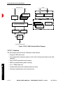
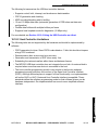
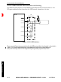
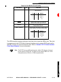
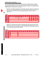
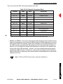
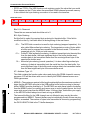
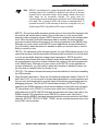
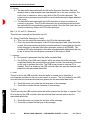
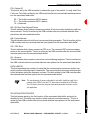
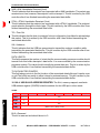
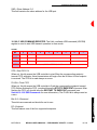
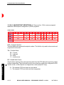
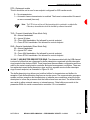
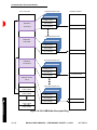
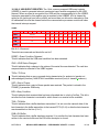
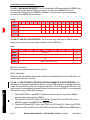
Communication Processor Module
Note: This update includes documentation on the full implementation of host mode, which is available for
Revision B MPC823 silicon and subsequent. Earlier revisions of the MPC823 support high speed (12
Mbs) Host Mode operation only.
The universal serial bus (USB) is an industry standard extension to the PC architecture. The
USB controller allows the MPC823 to exchange data with a PC host. It supports data
exchanges between a host computer and a wide range of simultaneously accessible
peripherals. The attached peripherals share USB bandwidth through a host scheduled
token-based protocol. The USB physical interconnect is a tiered star topology. A hub is at
the center of each star. Each wire segment is a point-to-point connection between the host
and a hub or function or a hub connected to another hub/function. There is only one host in
any USB system. The USB transfers signal and power over a four-wire cable. The signalling
occurs over two wires and point-to-point segments. The USB full-speed signalling bit rate is
12Mbps. A limited capability low-speed signalling mode is also defined at 1.5Mbps.
USB
16.10 UNIVERSAL SERIAL BUS CONTROLLER
The MPC823 USB controller consists of a transmitter module, receiver module, and two
protocol state machines. The protocol state machines control the receiver and transmitter
modules. One state machine implements the function state diagram and the other
implements the host state diagram. The MPC823 USB controller is capable of implementing
a USB function endpoint, a USB host, or both for testing purposes (loop-back diagnostics).
Figure 16-105 illustrates the USB controller block diagram.
For USB implementation, it is recommended that you get a copy of the USB Specification
as a supplement to this manual. You can download a copy from http://www.usb.org.
16
COMMUNICATION
The USB transmitter contains four independent FIFOs, each containing 16 bytes. There is
a dedicated FIFO for each of the four supported endpoints. The USB receiver has a single
16-byte FIFO. When the USB controller is not enabled in the USMOD, it consumes minimal
power.
MOTOROLA
MPC823 USER’S MANUAL -- PRELIMINARY UPDATE -- 9.25.98
16-314
Communication Processor Module
U-BUS
PERIPHERAL BUS
PORT CONTROL
USB
TX DATA FIFO
TX DATA FIFO
TX DATA FIFO
TX DATA FIFO
RX FIFO
MODE REGISTER
COMMAND REGISTER
PORT CONFIGURATION
USB FUNCTION ENDPOINT
AND HOST STATE MACHINES
RECEIVER
ADDRESS
REGISTER
ENDPOINT
REGISTERS
TRANSMITTER
DPLL/
BUS
INTERFACE
EXTERNAL TRANSCEIVER
Figure 16-105. USB Controller Block Diagram
16.10.1 Features
The following list summarizes the USB slave mode features:
• Supports USB slave mode
• Four independent endpoints support control, bulk, interrupt and isochronous data
transfers
• CRC16/CRC5 generation and checking
• NRZI encoding/decoding with bit stuffing
16
• 12 or 1.5Mbps data rate
COMMUNICATION
PROCESSOR MODULE
• Automatic retransmission upon transmit error
• Flexible data buffers with multiple buffers per frame
16-315
MPC823 USER’S MANUAL -- PRELIMINARY UPDATE -- 9.25.98
MOTOROLA
Communication Processor Module
The following list summarizes the USB host controller features:
• Supports control, bulk, interrupt, and isochronous data transfers
• CRC16 generation and checking
USB
• NRZI encoding/decoding with bit stuffing
• 12 and 1.5 Mbps data rates (automatic generation of PRE token and data rate
configuration)
• Flexible data buffers with multiple buffers per frame
• Supports local loopback mode for diagnostics (12 Mbps only).
For more details see Section 16.10.9 Using the USB Controller as a Host.
16.10.2 Host Controller Limitations
The following tasks are not supported by the hardware and should be implemented by
software:
• CRC5 generation for token. Since CRC5 is calculated on 11 bits, this should not impose
a large CPU overhead.
• Retransmission after an error and error recovery.
• Generation and transmission of SOF token every 1ms.
• Scheduling the various transfers within frame and between frames.
• The MPC823 USB host controller does not integrate the root hub. An external hub is
required when more than one device is connected to the host.
16
COMMUNICATION
• The host controller programming model is very similar to the function endpoint
programming model and does not conform to the Open Host Controller Interface
(OHCI). Although Motorola plans to support full host functionality, our implementation
will not be OHCI or UHCI (Universal Host Controller Interface) compatible. Those
standards define the software programming model so that software drivers can be
hardware-independent. Our implementation has a much more simplified software
interface.
MOTOROLA
MPC823 USER’S MANUAL -- PRELIMINARY UPDATE -- 9.25.98
16-316
Communication Processor Module
16.10.3 USB Controller Pin Functions and Clocking
The USB controller interfaces to the USB through a differential line driver and receiver. The
OE signal enables the line driver when the USB controller transmits on the bus.
USB
MPC823
USB
TRANSCEIVER
USBOE
USBTXP
D+
USBTXN
D-
+
USBRXD
–
USBRXP
USBRXN
Figure 16-106. USB Interface
There are six I/O port pins associated with the USB port and their functionality is described in
Table 16-30. Some transceivers may need additional control lines (speed select or
low-power control), which can be supported by the general-purpose output lines.
16
COMMUNICATION
PROCESSOR MODULE
16-317
MPC823 USER’S MANUAL -- PRELIMINARY UPDATE -- 9.25.98
MOTOROLA
Communication Processor Module
PIN SYMBOL
I/O
FUNCTION
USBTXN, USBTXP
O
Outputs from the USB transmitter, inputs to the
differential driver.
TP
TN
RESULT
0
0
1
1
0
1
0
1
single ended “0”
logic “0”
logic “1”
n/a
USBOE
O
Output Enable. Active low, enables the
transceiver to transmit data on the bus.
USBRXD
I
Receive Data. Input the USB receiver from the
differential line receiver.
UBRXP, USBRXN
I
Gated version of D+ and D-. Used to detect
single-ended zero, and interconnect speed.
RP
RN
RESULT
0
1
0
1
0
0
1
1
single ended “0”
full speed
low speed
n/a
USB
Table 16-30. USB Pin Functionality
The USB controller accepts a reference clock that is four times the USB bit rate. This clock
is programmed in the R1CS field of the serial interface clock register (SICR) and used by
the DPLL circuitry to recover the bit rate clock. Refer to Section 16.7.5.3 Serial Interface
Clock Route Register for more information.
16
COMMUNICATION
Note: The MPC823 can run at different frequencies, but the USB reference clock must
be four times the USB bit rate. The reference clock must be 48MHz for a 12Mb
full-speed transfer or 6MHz for a 1.5Mb low-speed transfer.
MOTOROLA
MPC823 USER’S MANUAL -- PRELIMINARY UPDATE -- 9.25.98
16-318
Communication Processor Module
16.10.4 Transmission and Reception Process
USB
After reset, the USB controller is addressable at the default address (0x00). During the
enumeration process, the host assigns a unique address to the USB controller. The software
should program the USB address register with the assigned address. The USB controller
supports four independent endpoints, which can each be configured to support control,
interrupt, bulk, or isochronous transfers modes when you program the USB endpoint
registers.
Note: You must configure endpoint 0 as a control transfer type. This endpoint is used
by the USB system software as a control pipe and any additional control pipes
may be provided by other endpoints.
Once enabled, the USB controller looks for valid token packets. Tokens that are not valid
(the PID or CRC check fails or the packet length is not 3 bytes) are ignored.
RESET
UNENUMERATED
ENUMERATION
PROCESS
IDLE
SETUP
TOKEN
SOF
TOKEN
IN
TOKEN
OUT
TOKEN
SETUP
SOF
TRANSMIT
RECEIVE
16
Figure 16-107. USB Controller Operating Modes
COMMUNICATION
PROCESSOR MODULE
16-319
MPC823 USER’S MANUAL -- PRELIMINARY UPDATE -- 9.25.98
MOTOROLA
16.10.4.1 OUT TOKEN. When the USB controller receives an OUT token, data reception
begins. The USB controller fetches the next buffer descriptor associated with the endpoint
and if it is empty, it starts transferring the incoming packet to the buffer descriptor’s
associated data buffer. When the data buffer has been filled, the USB controller clears the
E bit in the buffer descriptor and generates an interrupt if the I bit in the buffer descriptor is
set. If the incoming packet exceeds the length of the data buffer, the USB controller fetches
the next buffer descriptor in the table and, if it is empty, continues transferring the rest of the
packet to this buffer descriptor’s associated buffer. Otherwise, if it is full, an error occurs. The
entire data packet, including the DATA0/DATA1 packet ID (PID), is written to the receive
buffers and the PID is reflected in the PID field of the receive buffer descriptor. It is your
responsibility to program the driver software to check data packet synchronization by
monitoring the DATA0/DATA1 PID sequence toggle.
USB
Communication Processor Module
Table 16-31. USB Out Token Reception
DATA PACKET
CORRUPTED
USEPx
RHS FIELD
HANDSHAKE
SENT TO HOST
Yes
N/A
None (Data Discarded)
No
00 (Normal)
ACK
No
01 (Ignore)
None
No
10 (NAK)
NAK
No
11 (STALL)
STALL
16
COMMUNICATION
If the packet was received error-free (no CRC errors and no bit stuff error), depending on
the endpoint transfer mode configuration, an ACK handshake will be transmitted to the host.
If a reception error occurred, no handshake packet is returned, and the error status bits will
be set in the last buffer descriptor associated with this packet. If the RHS field in the
endpoint’s configuration register is programmed to respond with NAK, a NAK handshake is
returned instead of ACK. If the RHS field is programmed to respond with STALL, a STALL
handshake is returned. In both cases, the buffer will receive the data packet if the buffer
descriptors are available.
MOTOROLA
MPC823 USER’S MANUAL -- PRELIMINARY UPDATE -- 9.25.98
16-320
Communication Processor Module
16.10.4.2 IN TOKEN. To guarantee data transfer, the control software must preload the
endpoint FIFO with a data packet prior to receiving an IN token. The software should set up
the endpoint transmit buffer descriptor table and set the STR bit in the USB command
register. The USB controller will fill the transmit FIFO and wait until it receives the IN token.
Once it is received and the FIFO is loaded with the last byte of the data, or at least with 4
bytes, transmission begins.
USB
Table 16-32. USB In Token Reception
FIFO LOADED
WITH DATA
USEPx
THS FIELD
HANDSHAKE
SENT TO HOST
No
00 (Normal)
NAK
Yes
00 (Normal)
ACK
N/A
01 (Ignore)
None
N/A
10 (NAK)
NAK
N/A
11 (STALL)
STALL
If data is not ready in the transmit FIFO or if the THS field in the endpoint’s configuration
register is set to respond with NAK, a NAK handshake is returned. If the THS field in the
endpoint’s configuration register is set to respond with STALL, a STALL handshake is
returned. When the end of the current buffer descriptor has been reached and the last buffer
in the packet bit is set, the CRC is appended. Following the transmission of a frame, the USB
controller waits for a handshake packet, depending on the configuration of the endpoint. If
the host fails to acknowledge the packet, the timeout status bit will be set in the buffer
descriptor. It is your responsibility to program the driver software to set the proper
DATA0/DATA1 PID in the transmitted packet.
16
COMMUNICATION
PROCESSOR MODULE
16.10.4.3 SETUP TOKEN. Setup transactions are similar in format to an OUT token, but
you should use a SETUP rather than an OUT PID. A SETUP token is only recognized by an
endpoint that is configured as a control endpoint. Once the SETUP token is received, setup
data reception begins. The USB controller fetches the next buffer descriptor associated with
the endpoint, and if it is empty, starts transferring the incoming packet to the buffer
descriptor’s associated data buffer. When the data buffer has been filled, the USB controller
clears the E bit in the buffer descriptor and generates an interrupt if the I bit in the buffer
descriptor is set. If the incoming packet exceeds the length of the data buffer, the USB
controller fetches the next buffer descriptor in the table and, if it is empty, continues
transferring the rest of the packet to this buffer descriptor’s associated buffer. If it is full, an
error occurs. The entire data packet including the DATA0 PID are written to the receive
buffers. If the packet was received error-free (no CRC errors and no bit stuff error) an ACK
handshake will be transmitted to the host. If a reception error occurred, no handshake
packet will be returned and the error status bits will be set in the last buffer descriptor
associated with this packet.
16-321
MPC823 USER’S MANUAL -- PRELIMINARY UPDATE -- 9.25.98
MOTOROLA
Communication Processor Module
16.10.4.5 PRE TOKEN. The PRE token signals the hub that a low-speed transaction is
about to occur. The PRE token is only read by the hub. The USB controller ignores the PRE
token in slave mode. In host mode, the USB controller generates a full speed PRE token
before any packet sent to a low speed peripheral.
USB
16.10.4.4 SOF TOKEN. When a start of frame (SOF) token packet is received, the USB
controller issues a SOF maskable interrupt and the frame number entry in the parameter
RAM is updated.
16.10.5 USB Controller Parameter RAM Memory Map
The USB controller parameter RAM area begins at the USB base address. The area is used
for the general USB parameters. Notice that it is similar to the SCC2 general-purpose
parameter RAM.
Table 16-33. USB Parameter RAM Memory Map
ADDRESS
NAME
WIDTH
DESCRIPTION
USB Base + 00
EP0PTR
Half Word
Endpoint 0 Register
USB Base + 02
EP1PTR
Half Word
Endpoint 1 Register
USB Base + 04
EP2PTR
Half-Word
Endpoint 2 Register
USB Base + 06
EP3PTR
Half Word
Endpoint 3 Register
USB Base + 08
RSTATE
Word
RX Internal State
USB Base + 0C
RPTR
Word
RX Internal Data Pointer
USB Base + 10
FRAME_N
Half Word
Frame Number
USB Base + 12
RBCNT
Half-Word
RX Internal Byte Count
USB Base + 14
RTEMP
Word
RX Temp
16
COMMUNICATION
NOTE: You are only responsible for initializing the items in bold.
USB Base = (IMMR & 0xFFFF0000) + 0x3C00.
All references to registers in the parameter RAM table are actually implemented in the dual-port RAM
area as a memory-based register.
MOTOROLA
MPC823 USER’S MANUAL -- PRELIMINARY UPDATE -- 9.25.98
16-322
Communication Processor Module
You must initialize certain parameter RAM values before the USB controller is enabled.
Other values are initialized by the communication processor module. Once initialized, the
parameter RAM values do not need to be accessed by your software. They should only be
modified when no USB activity is in progress.
USB
• EPxPTR—The endpoint parameters block pointers are index pointers to the endpoint’s
parameter block. The parameter block can be allocated to any address divisible by 32
in the dual-port RAM. The format of the endpoint parameter block is shown in
Table 16-34.
EPxPTR
BIT
0
1
2
3
4
5
6
7
8
9
10
11
12
13
14
15
FIELD
ENDPOINT INDEX POINTER
0
0
0
0
0
R/W
R/W
R/W
R/W
R/W
R/W
R/W
RESET
0
0
0
0
0
0
ADDR
USB BASE + 0x00 (EP0PTR), 0x02 (EP1PTR), 0x04 (EP2PTR), 0x06 (EP3PTR)
• FRAME_N—The frame number entry is updated by the USB controller when a SOF
token is received. The entry contains 11 bits representing the frame number. An SOF
interrupt is issued when this entry is updated. The user should initialize this parameter
to zero before operating the USB controller.
FRAME_N
BIT
0
FIELD
V
RESERVED
FRAME NUMBER
R/W
R/W
R/W
R/W
RESET
0
0
0
ADDR
1
2
3
4
5
6
7
8
9
10
11
12
13
14
15
USB BASE + 0x10
16
COMMUNICATION
PROCESSOR MODULE
16-323
MPC823 USER’S MANUAL -- PRELIMINARY UPDATE -- 9.25.98
MOTOROLA
Communication Processor Module
The V bit is set if the SOF token was received error-free.
ADDRESS
NAME
WIDTH
DESCRIPTION
Base + 00
RBASE
Half Word
RX BD Base Address
Base + 02
TBASE
Half Word
Tx BD Base Address
Base + 04
RFCR
Byte
RX Function Code
Base + 05
TFCR
Byte
TX Function Code
Base + 06
MRBLR
Half Word
Maximum Receive Buffer Length
Base + 08
RBPTR
Half Word
RX BD Pointer
Base + 0a
TBPTR
Half Word
TX BD Pointer
Base + 0c
TSTATE
Word
TX Internal State
Base + 10
TPTR
Word
TX Internal Data Pointer
Base + 14
TCRC
Half Word
TX Temp CRC
Base + 16
TBCNT
Half Word
TX Internal Byte Count
Base + 18
RES
8 Bytes
Reserved
USB
Table 16-34. Endpoint Parameters Block
NOTE: You are only responsible for initializing the items in bold. Also, Base = (EP x PTR).
• RBASE and TBASE—The receive and transmit buffer descriptor base address entries
define the starting point in the dual-port RAM for the set of buffer descriptors to receive
and transmit data. This provides a great deal of flexibility in how buffer descriptors for
the USB controller are partitioned. By setting the W bit in the last buffer descriptor in
each list, you can select how many buffer descriptors to allocate for the transmit and
receive side of the USB controller. However, you must initialize these entries before
enabling the USB controller. Furthermore, you should not configure buffer descriptor
tables of the USB to overlap any other serial channel’s buffer descriptors or else erratic
operation will occur.
16
COMMUNICATION
Note: RBASE and TBASE should contain a value that is divisible by 8.
MOTOROLA
MPC823 USER’S MANUAL -- PRELIMINARY UPDATE -- 9.25.98
16-324
Communication Processor Module
• RFCR and TFCR—The USB function code registers control the value that you would
like to appear on the AT pins when the associated SDMA channel accesses memory.
It also controls the byte-ordering convention to be used in the transfers.
RFCR AND TFCR
USB
BIT
0
FIELD
1
RESERVED
2
3
4
5
BO
6
7
AT
Bits 0–2—Reserved
These bits are reserved and should be set to 0.
BO—Byte Ordering
Set this field to select the required byte ordering for the data buffer. If this field is
modified on-the-fly, it will take effect at the beginning of the next frame.
00 =
The DEC/Intel convention is used for byte ordering (swapped operation). It is
also called little-endian byte ordering. The transmission order of bytes within
a buffer word is reversed as compared to the Motorola mode. This mode is
supported only for 32-bit port size memory.
01 = PowerPC little-endian byte ordering. As data is transmitted onto the serial line
from the data buffer, the least-significant byte of the buffer double-word
contains data to be transmitted earlier than the most-significant byte of the
same buffer double word.
1X = Motorola byte ordering (normal operation). It is also called big-endian byte
ordering. As data is transmitted onto the serial line from the data buffer, the
most-significant byte of the buffer word contains data to be transmitted earlier
than the least-significant byte of the same buffer word.
AT—Address Type 1–3
This field contains the function code value used during this SDMA channel’s memory
accesses. AT0 will be driven with a one to identify this SDMA channel access as a
DMA-type access.
16
• MRBLR—The maximum receive buffer length register defines the maximum number of
bytes that the MPC823 will write to the USB receive buffer before moving to the next
buffer. MRBLR must be divisible by 4. The MPC823 can write fewer bytes to the buffer
than the MRBLR value if a condition such as an error or end-of-packet occurs, but it will
never write more bytes than the MRBLR value. It follows, then, that buffers you supply
to the MPC823 should always be at least as long as MRBLR.
COMMUNICATION
PROCESSOR MODULE
The transmit buffers for the USB channel are not affected in any way by the value
programmed into MRBLR. Transmit buffers may be individually chosen to have varying
lengths, as needed. The number of bytes to be transmitted is chosen by programming
the DATA LENGTH field in the TX buffer descriptor.
16-325
MPC823 USER’S MANUAL -- PRELIMINARY UPDATE -- 9.25.98
MOTOROLA
Note: MRBLR is not intended to be changed dynamically while the USB channel is
operating. However, if it is modified in a single bus cycle with one 16-bit move
(not two 8-bit bus cycles back-to-back), then a dynamic change in the receive
buffer length can be successfully achieved. This occurs when the
communication processor module moves control to the next RX buffer descriptor
in the table. Thus, a change to MRBLR will not have an immediate effect. To
guarantee the exact RX buffer descriptor on which the change will occur, you
should change MRBLR only while the USB receiver is disabled.
USB
Communication Processor Module
• RBPTR—The receiver buffer descriptor pointer points to the next buffer descriptor that
the receiver will transfer data to when it is in an idle state or to the current buffer
descriptor while processing a frame. RBPTR should be initialized by the software after
reset. When the end of the buffer descriptor table is reached, the communication
processor module initializes this pointer to the value programmed in the RBASE entry.
Although you never need to write RBPTR in most applications (except initialization),
you can modify it when the receiver is disabled or when you are sure that no receive
buffer is currently in use.
• TBPTR—The transmitter buffer descriptor pointer for each USB endpoint points to the
next buffer descriptor that the transmitter will transfer data from when it is in an idle state
or to the current buffer descriptor during frame transmission. TBPTR should be
initialized by the software after reset. When the end of buffer descriptor table is reached,
the communication processor module initializes this pointer to the value programmed
in the TBASE entry. Although you never need to write TBPTR in most applications
(except initialization), you can modify it when the transmitter is disabled or when you
are sure that no transmit buffer is currently in use.
• TSTATE—The transmit internal state entry should be initilaized to zero before enabling
the USB controller.
• Other General Parameters—These are the additional parameters listed in Table 16-33
and Table 16-34. You do not need to access these parameters in normal operation and
they are only listed because they provide helpful information to experienced users for
debugging purposes. The RX and TX internal data pointers (RPTR and TPTR) are
updated by the SDMA channels to show the next address in the buffer to be accessed.
16
COMMUNICATION
TX internal byte count (TBCNT) is a down-count value that is initialized with the TX
buffer descriptor’s DATA LENGTH field and decremented with every byte read by the
SDMA channels. RX internal byte count (RBCNT)is a down-count value that is
initialized with the MRBLR value and decremented with every byte written by the SDMA
channels. RSTATE, TSTATE, RTEMP, TTEMP, and the reserved areas are only used
by the RISC microcontroller.
MOTOROLA
MPC823 USER’S MANUAL -- PRELIMINARY UPDATE -- 9.25.98
16-326
Communication Processor Module
16.10.6 USB Commands
You can program the CPM command register (CPCR) with the following commands to
transmit data.
USB COMMAND FORMAT (CPCR)
USB
BIT
0
FIELD
RST
RESET
R/W
1
2
4
5
6
7
8
9
10
11
USBCMD
1
1
1
1
0
0
0
0
0
0
0
0
0
0
0
0
0
R/W
RW/
R/W
R/W
R/W
R/W
R/W
R/W
R/W
ADDR
3
12
13
14
15
ENDPOINT
RES
FLG
0
0
0
0
R/W
R/W
R/W
R/W
(IMMR & 0xFFFF0000) + 0x9C0
• RST—The reset bit is set by the core and cleared by the communication processor
module and when this command is executed, RST and FLG are cleared within two
general system clocks. The RISC microcontroller reset routine is approximately 60
clocks long, but you can start initializing the communication processor module
immediately after this command is issued. RST is useful when the core wants to reset
the registers and parameters for all the channels as well as the RISC microprocessor
and timer tables. However, this bit does not affect the serial interface or parallel I/O
registers.
• USBCMD—This field contains the USB command
001 = The STOP TX ENDPOINT command disable the transmission of data on the
selected endpoint. After you issue the command, flush the corresponding
endpoint FIFO. No further transmissions will occur until the RESTART TX
ENDPOINT command is issued.
010 = The RESTART TX ENDPOINT command enables the transmission of data
from the corresponding endpoint on the USB. This command is expected by
the USB controller after a STOP TX ENDPOINT command or after a
transmission error (underrun or timeout) occurs.
000 = Reserved.
011 = Reserved.
100 = Reserved.
101 = Reserved.
110 = Reserved.
111 = Reserved.
• ENDPOINT—This bit is the logical pipe number.
16
COMMUNICATION
PROCESSOR MODULE
00 =
01 =
10 =
11 =
16-327
Endpoint 0.
Endpoint 1.
Endpoint 2.
Endpoint 3.
MPC823 USER’S MANUAL -- PRELIMINARY UPDATE -- 9.25.98
MOTOROLA
Communication Processor Module
• FLG—The bit is set by the core and cleared by the communication processor module.
The communication processor module is ready to receive a new command.
The CPCR contains a command that the communication processor module is
currently processing. The communication processor module clears this bit
when the command finishes executing or after reset.
USB
0=
1=
For additional opcode information, see Table 16-2.
16.10.7 USB Controller Errors
The USB controller reports frame reception and transmission error conditions using the
channel buffer descriptors and the USB event register. The following transmission errors
can be detected by the USB controller.
• Transmit Underrun Error—If this error occurs, the channel forces a bit-stuffing violation,
terminates buffer transmission, closes the buffer, sets the UN bit in the TX buffer
descriptor, and sets the corresponding TXE bit in the USB event register. The endpoint
resumes transmission after the RESTART TX ENDPOINT command is received.
• Transmit Timeout Error—If this error occurs, the channel tries to retransmit if the RTE
bit is set in the USB endpoint configuration register. If the RTE bit is not set or the
second attempt fails, the channel closes the buffer, sets the TO bit in the TX buffer
descriptor, and sets the corresponding TXEx bit in the USB event register. The endpoint
resumes transmission after the RESTART TX ENDPOINT command is received.
The following reception errors can be detected by the USB controller.
• Overrun Error—The USB controller maintains an internal FIFO for receiving data. If a
receive overrun occurs, the channel writes the received data byte to the internal FIFO
over the previously received byte. The channel closes the buffer, sets the OV bit in the
buffer descriptor, and sets the RXB bit in the USB event register. The NAK handshake
is transmitted at the end of the received packet if the packet was error-free.
• Busy Error—A frame was received and discarded due to a lack of buffers. The channel
sets the BSY bit in the USB event register.
• Non Octet Aligned Packet Error—If this error occurs, the channel writes the received
data to the data buffer, closes the buffer, sets the NO bit in the RX buffer descriptor, and
generates a RXB interrupt.
16
COMMUNICATION
• CRC Error—When a CRC error occurs, the channel closes the buffer, and sets the CR
bit in the RX buffer descriptor and the RXB bit in the USB event register. In isochronous
mode, the USB controller reports a CRC error, however, there are no handshake
packets (ACK) and the transfer continues normally when an error occurs.
MOTOROLA
MPC823 USER’S MANUAL -- PRELIMINARY UPDATE -- 9.25.98
16-328
Communication Processor Module
16.10.8 USB Controller Programming Model
16.10.8.1 USB MODE REGISTER. The read/write USB mode (USMOD) register controls
the USB controller’s operation mode.
USMOD
USB
BIT
0
1
FIELD
LSS
RESUME
RESET
0
R/W
R/W
ADDR
2
3
4
5
6
7
RESERVED
TEST
HOST
EN
0
0
0
0
0
R/W
R/W
R/W
R/W
R/W
(IMMR & 0xFFFF0000) + 0xA00
LSS—Low-Speed Signaling
When set, this bit selects low-speed (1.5Mbps) signaling. The actual bit rate depends on the
USB clock source.
0 = Full-speed (12Mbps) signaling. Normal operation mode.
1 = Low-speed (1.5Mbps) signaling. This mode can be used for a point-to-point
connection to a low-speed device or in local loopback mode.
RESUME—Generate Resume Condition
When set, this bit generates a resume condition on the USB. This bit should be used if the
function wants to exit suspend mode.
Bits 2–4—Reserved
These bits are reserved and should be set to zero.
TEST—Test Mode
0 = Normal operation.
1 = Local loopback mode. In this mode, if the HOST bit is set, endpoint 0 operates as
host and endpoints 1–3 can be used as function endpoints.
HOST—Host Mode
0 = The USB controller implements a USB function.
1 = The USB controller implements a USB host. Endpoint 0 operates as the host. The
other endpoints are not used, unless the TEST bit is set.
16
COMMUNICATION
PROCESSOR MODULE
16-329
MPC823 USER’S MANUAL -- PRELIMINARY UPDATE -- 9.25.98
MOTOROLA
Communication Processor Module
EN—Enable USB
This bit enables USB operation. When the EN bit is cleared, the USB is in a reset state and
consumes minimal power.
USB
0 = USB is disabled.
1 = USB is enabled.
Note: You should not modify any other bits of the USMOD register while the EN bit is
set.
16.10.8.2 USB RECEIVE BUFFER DESCRIPTOR. The USB controller reports
information about each buffer of received data using (RX) buffer descriptors. The USB
controller closes the current buffer, generates a maskable interrupt, and starts receiving
data in the next buffer when the current buffer is full. Additionally, it will close the buffer under
the following conditions:
• When an end of packet is detected
• When an overrun error occurs
• When a bit stuff violation is detected
Note: The buffer descriptor’s status bits are sticky. Applications that operate on those
bits may need to be reset after every relevant CPM transaction.
The first word of the RX buffer descriptor contains status and control bits. You should
prepare these bits before reception because they are set by the USB controller after the
buffer has been closed. The second word contains the data length, in bytes, that was
received. The third and fourth words contain a pointer that always points to the beginning of
the received data buffer.
BIT
0
1
2
3
4
5
OFFSET + 0
E
RES
W
I
L
F
OFFSET + 2
6
7
RES
8
9
PID
10
11
12
13
14
15
RES
NO
AB
CR
OV
RES
DATA LENGTH
OFFSET + 4
TX DATA BUFFER POINTER
OFFSET + 6
16
COMMUNICATION
NOTE: You are only responsible for initializing the items in bold.
MOTOROLA
MPC823 USER’S MANUAL -- PRELIMINARY UPDATE -- 9.25.98
16-330
Communication Processor Module
USB
E—Empty
0 = The data buffer associated with this RX buffer descriptor has been filled with
received data or data reception has been aborted due to an error condition. The
core is free to examine or write to any fields of this RX buffer descriptor. The
communication processor module will not use this buffer descriptor again when the
E bit is zero.
1 = The data buffer associated with this buffer descriptor is empty or reception is
currently in progress. This RX buffer descriptor and its associated receive buffer
are owned by the communication processor module. Once the E bit is set, the core
should not write any fields to this RX buffer descriptor.
Bits 1, 9–10, and 15—Reserved
These bits are reserved and should be set to 0.
W—Wrap (Final Buffer Descriptor in Table)
0 = This is not the last buffer descriptor in the RX buffer descriptor table.
1 = This is the last buffer descriptor in the RX buffer descriptor table. After this buffer
is used, the communication processor module receives incoming data into the first
buffer descriptor in the table (the buffer descriptor pointed to by RBASE). The
number of RX buffer descriptors in this table is programmable and determined only
by the W bit and the overall space constraints of the dual-port RAM.
I—Interrupt
0 = No interrupt is generated after this buffer has been filled.
1 = The RXB bit in the USB event register will be set when this buffer has been
completely filled by the communication processor module, thus indicating the need
for the core to process the buffer. The RXB bit can cause an interrupt if it is
enabled. This bit is written by the USB controller after the received data has been
placed into the associated data buffer.
L—Last
This bit is set by the USB controller when the buffer is closed due to detection of
end-of-packet condition on the bus or as a result of an error. This bit is written by the USB
controller after the received data has been placed into the associated data buffer.
0 = This buffer does not contain the last character of the message.
1 = This buffer contains the last character of the message.
16
COMMUNICATION
PROCESSOR MODULE
F—First
This bit is set by the USB controller when the buffer contains the first byte of a packet. This
bit is written by the USB controller after the received data has been placed into the
associated data buffer.
0 = This buffer does not contain the first byte of the message.
1 = This buffer contains the last byte of the message.
16-331
MPC823 USER’S MANUAL -- PRELIMINARY UPDATE -- 9.25.98
MOTOROLA
Communication Processor Module
PID—Packet ID
This field is set by the USB controller to indicate the type of the packet. It is only valid if the
F bit is set. This field is written by the USB controller after the received data has been placed
into the associated data buffer.
USB
00 = This buffer contains a DATA0 packet.
01 = This buffer contains a DATA1 packet.
1X = Reserved.
NO—RX Non Octet Aligned Packet
This bit indicates that a packet containing a number of bits not exactly divisible by eight has
been received. This bit is written by the USB controller after the received data has been
placed into the associated data buffer.
AB—Frame Aborted
This bit indicates that a bit stuff error has occurred during reception. This bit is written by the
USB controller after the received data has been placed into the associated data buffer.
CR—CRC Error
This bit indicates that a frame contains a CRC error. The received CRC bytes are always
written to the receive buffer. This bit is written by the USB controller after the received data
has been placed into the associated data buffer.
OV—Overrun
This bit indicates that a receiver overrun has occurred during reception. This bit is written by
the USB controller after the received data has been placed into the associated data buffer.
DATA LENGTH
This field represents the number of octets that the communication processor module has
written into this buffer descriptor’s data buffer. The communication processor module writes
to this field when the buffer descriptor is closed. This bit is written by the USB controller after
the received data has been placed into the associated data buffer.
16
RX DATA BUFFER POINTER
This field always points to the first location of the associated data buffer and must be
divisible by four. The buffer may reside in either internal or external memory. This bit is
written by the USB controller after the received data has been placed into the associated
data buffer.
COMMUNICATION
Note: The actual amount of memory allocated for this buffer should be equal to the
contents of the MRBLR, plus two CRC bytes that are included in the RX buffer.
The USB device driver may strip out these two bytes before the data is sent to
your application.
MOTOROLA
MPC823 USER’S MANUAL -- PRELIMINARY UPDATE -- 9.25.98
16-332
Communication Processor Module
16.10.8.3 USB TRANSMIT BUFFER DESCRIPTOR. Data to be transmitted with the USB
is presented to the communication processor module by arranging it in buffers referenced
by the transmit (TX) buffer descriptor ring. The first word of the TX buffer descriptor contains
status and control bits.
USB
BIT
0
1
2
3
4
5
OFFSET + 0
R
RES
W
I
L
TC
OFFSET + 2
6
7
CNF LSP
8
9
PID
10
RES
11
12
NAK STAL
13
14
15
TO
UN
RES
DATA LENGTH
OFFSET + 4
TX DATA BUFFER POINTER
OFFSET + 6
NOTE: You are only responsible for initializing the items in bold.
Note: The communication processor module sets all the status bits in this buffer
descriptor. You should clear all the status bits before submitting the buffer
descriptor to the communication processor module. For example, the parity error
bit is only set when a parity error occurs.
R—Ready
0 = The data buffer associated with this buffer descriptor is not ready for transmission.
You are free to manipulate this buffer descriptor or its associated data buffer. The
communication processor module clears this bit after the buffer has been
transmitted or after an error condition is encountered.
1 = The data buffer, which you have prepared for transmission, has not been
transmitted or is currently being transmitted. You cannot write to the fields of this
buffer descriptor once this bit is set.
Bits 1, 6–12, and 15—Reserved
These bits are reserved and should be set to 0.
16
COMMUNICATION
PROCESSOR MODULE
W—Wrap (Final Buffer Descriptor in Table)
0 = This is not the last buffer descriptor in the TX buffer descriptor table.
1 = This is the last buffer descriptor in the TX buffer descriptor table. After this buffer
has been used, the communication processor module will transmit incoming data
from the first buffer descriptor in the table (the buffer descriptor pointed to by
TBASEx). The number of TX buffer descriptors in this table is programmable and
is determined only by the W bit and the overall space constraints of the dual-port
RAM.
16-333
MPC823 USER’S MANUAL -- PRELIMINARY UPDATE -- 9.25.98
MOTOROLA
Communication Processor Module
I—Interrupt
0 = No interrupt is generated after this buffer has been serviced.
1 = The TXB or the appropriate TXEx bit in the USBER is set when this buffer is
serviced. TXB and TXEx can cause interrupts if they are enabled.
USB
L—Last
0 = This buffer does not contain the last character of the message.
1 = This buffer contains the last character of the message.
TC—Transmit CRC
This bit is only valid when the L bit is set. Otherwise, it is ignored.
0 = Transmit end-of-packet after the last data byte. This setting can be used for testing
purposes to send a bad CRC after the data.
1 = Transmit the CRC sequence after the last data byte.
CNF—Transmit Confirmation
This bit is only valid when the L bit is set. Otherwise, it is ignored. It only affects endpoints
which have the MF bit set in the endpoint configuration register (ISO mode endpoint or host).
0 = Continue to load the transmitter FIFO with the next packet. No handshake or
response is expected from the function for this packet.
1 = Wait for handshake or response from the function before stating the next packet or
this is the last packet.
Note: You cannot set CNF = 0 for a token that should be followed by a data packet if
the data packet buffer descriptor is not ready.
LSP - Low Speed Transaction (Host).
0 = The following transaction is with the host or a full speed device.
1 = The following transaction is with a low speed device (required only for data buffers
containing a token)..
Note: You should always set LSP = 0 in slave mode.
COMMUNICATION
PID—Packet ID
This bit field is valid for the first BD of a packet; otherwise it is ignored.
16
0X = Do not append PID to the data.
10 = Transmit DATA0 PID before sending the data.
11 = Transmit DATA1 PID before sending the data.
MOTOROLA
MPC823 USER’S MANUAL -- PRELIMINARY UPDATE -- 9.25.98
16-334
Communication Processor Module
NAK—NAK Handshake Received (Host)
This bit indicates that the endpoint has responded with a NAK handshake. The packet was
received error-free, however, the endpoint could not accept it. This bit is written by the USB
controller after it has finished transmitting the associated data buffer.
USB
STAL—STALL Handshake Received (Host)
This bit indicates that the endpoint has responded with a STALL handshake. The endpoint
needs attention through the control pipe. This bit is written by the USB controller after it has
finished transmitting the associated data buffer.
TO—Time-Out
This bit indicates that the host (or endpoint for host configuration) has failed to acknowledge
this packet. This bit is written by the USB controller after it has finished transmitting the
associated data buffer.
UN—Underrun
This bit indicates that the USB has encountered a transmitter underrun condition while
transmitting the associated data buffer. This bit is written by the USB controller after it has
finished transmitting the associated data buffer.
DATA LENGTH
This field represents the number of octets that the communication processor module should
transmit from this buffer descriptor’s data buffer. It is never modified by the communication
processor module. This value should normally be greater than zero. This bit is written by the
USB controller after it has finished transmitting the associated data buffer.
TX DATA BUFFER POINTER
This field always points to the first location of the associated data buffer and it can be even
or odd.The buffer can reside in either internal or external memory. This bit is written by the
USB controller after it has finished transmitting the associated data buffer.
16.10.8.4 USB SLAVE ADDRESS REGISTER. The 8-bit, memory-mapped, read/write
USB address register (USADR) holds the address for this USB port in slave mode.
USADR
16
BIT
0
FIELD
RESERVED
SAD
RESET
0
0
R/W
R/W
R/W
COMMUNICATION
PROCESSOR MODULE
ADDR
1
2
3
4
5
6
7
(IMMR & 0xFFFF0000) + 0xA01
Bit 0—Reserved
This bit is reserved and should be set to 0.
16-335
MPC823 USER’S MANUAL -- PRELIMINARY UPDATE -- 9.25.98
MOTOROLA
Communication Processor Module
USB
SAD—Slave Address 0–6
This field contains the slave address for the USB port.
16.10.8.5 USB COMMAND REGISTER. The 8-bit, read/write USB command (USCOM)
register is used to start USB transmit operation in slave mode.
USCOM
BIT
0
1
FIELD
STR
FLUSH
RESERVED
EP
RESET
0
0
0
0
R/W
R/W
R/W
R/W
R/W
ADDR
2
3
4
5
6
7
(IMMR & 0xFFFF0000) + 0xA02
STR—Start FIFO Fill
When set, this bit causes the USB controller to start filling the corresponding endpoint
transmit FIFO with data. Actual transmission will begin once the IN token for this endpoint
is received. The STR bit is read always as a zero.
FLUSH—Flush FIFO
When set, this bit causes the USB controller to flush the corresponding endpoint transmit
FIFO. Before flushing the FIFO, you should issue the STOP TX ENDPOINT command. After
flushing the FIFO you should issue the RESTART TX ENDPOINT command (see
Section 16.10.6 USB Commands for more information). The FLUSH bit is always read as
a zero.
COMMUNICATION
Bits 2–5—Reserved
These bits are reserved and should be set to zero.
16
EP—Endpoint
This field selects one of the four supported endpoints.
MOTOROLA
MPC823 USER’S MANUAL -- PRELIMINARY UPDATE -- 9.25.98
16-336
Communication Processor Module
USB
16.10.8.6 USB ENDPOINT REGISTERS 0–3. There are four 16-bit, memory-mapped,
read/write USB endpoint configuration (USEPx) registers.
USEP0–USEP3
BIT
0
1
2
3
4
5
6
7
8
9
10
11
12
13
FIELD
EPN
RESERVED
TM
RESERVED
MF
RTE
THS
RESET
0
0
0
0
0
0
0
R/W
R/W
R/W
R/W
R/W
R/W
R/W
R/W
ADDR
14
15
RHS
R/W
(IMMR & 0xFFFF0000) + 0xA04 (USEP0), 0xA06 (USEP1), 0xA08 (USEP2), 0xA0A (USEP3)
EPN— Endpoint Number
This field defines the supported endpoint number. This field is only used in slave mode and
is ignored in host mode.
TM—Transfer Mode
00 = Control.
01 = Interrupt.
10 = Bulk.
11 = Isochronous.
16
MF—Enable Multi-Frame
This bit allows loading of the next transmit packet into the FIFO before the previous packet
finishes transmitting. This bit should be set to zero unless the endpoint is configured for ISO
transfer mode, or the endpoint is configured as a host (endpoint 0 only).
COMMUNICATION
PROCESSOR MODULE
0 = The transmit FIFO can hold only one packet.
1 = The transmit FIFO can hold more than one packet.
16-337
MPC823 USER’S MANUAL -- PRELIMINARY UPDATE -- 9.25.98
MOTOROLA
Communication Processor Module
RTE—Retransmit enable
This bit should be set to zero for an endpoint configured for ISO transfer mode.
USB
0 = No retransmission.
1 = Automatic frame retransmission is enabled. The frame is retransmitted if transmit
an error occurred (time-out).
Note: The RTE bit can only be set if the transmit packet is contained in a single buffer.
Other wise, retransmission should be handled by software intervention.
THS—Transmit Handshake (Slave Mode Only)
00 = Normal handshake.
01 = Ignore IN token.
10 = Force NAK handshake. Not allowed for control endpoint.
11 = Force STALL handshake. Not allowed for control endpoint.
RHS—Receive Handshake (Slave Mode Only)
00 = Normal handshake.
01 = Ignore OUT token.
10 = Force NAK handshake. Not allowed for control endpoint.
11 = Force STALL handshake. Not allowed for control endpoint.
16.10.8.7 USB BUFFER DESCRIPTOR RING. The data associated with the USB channel
is stored in buffers that are referenced by buffer descriptors organized in buffer descriptor
rings located in the dual-port RAM. These rings have the same basic configuration as those
used by the serial communication controller and serial management controllers. There are
four separate transmit buffer descriptor rings and four separate receive buffer descriptor
rings for each endpoint, as illustrated in Figure 16-108.
16
COMMUNICATION
The buffer descriptor ring allows you to define buffers for transmission and buffers for
reception. Each buffer descriptor ring forms a circular queue. The communication processor
module confirms reception and transmission or indicates error conditions using the buffer
descriptors to inform the processor that the buffers have been serviced. The actual buffers
can reside in either external memory or internal memory. Data buffers can reside in the
parameter RAM of a serial communication controller if it is not enabled.
MOTOROLA
MPC823 USER’S MANUAL -- PRELIMINARY UPDATE -- 9.25.98
16-338
Communication Processor Module
DUAL- PORT RAM
TX BUFFER DESCRIPTORS
EXTERNAL MEMORY
FRAME STATUS
USB
USBENDPOINT
ENDPOINT0 1
TX BD TABLE
DATA LENGTH
DATA POINTER
TX DATA BUFFER
TX BUFFER DESCRIPTORS
ENDPOINT 3
TX BD TABLE
FRAME STATUS
DATA LENGTH
DATA POINTER
ENDPOINT 0
TX DATA BUFFER
RX BUFFER DESCRIPTORS
RX BD TABLE
FRAME STATUS
DATA LENGTH
DATA POINTER
RX DATA BUFFER
ENDPOINT 3 RX BD
TABLE
RX BUFFER DESCRIPTORS
EP0 RX BD
TABLE POINTER
EP0 TX BD
TABLE POINTER
FRAME STATUS
16
DATA LENGTH
RX DATA BUFFER
EP3 RX BD
DATA POINTER
COMMUNICATION
PROCESSOR MODULE
TABLE POINTER
EP3 TX BD
TABLE POINTER
Figure 16-108. USB Buffer Descriptor Ring
16-339
MPC823 USER’S MANUAL -- PRELIMINARY UPDATE -- 9.25.98
MOTOROLA
16.10.8.8 USB EVENT REGISTER. The 16-bit, memory-mapped USB event register
(USBER) is used to generate interrupt events and report events recognized by the USB
channel. When an event is recognized, the USB sets the corresponding bit in the USBER.
Interrupts generated by this register may be masked in the USBMR. A bit is cleared by
writing a one (writing a zero has no effect) and more than one bit can be cleared at a time.
All unmasked bits must be cleared before the communication processor module will clear
the internal interrupt request.
USB
Communication Processor Module
USBER
BIT
0
1
2
3
4
5
6
7
8
9
10
11
12
13
14
15
FIELD
RESERVED
RESET
IDLE
TXE3
TXE2
TXE1
TXE0
SOF
BSY
TXB
RXB
RESET
0
0
0
0
0
0
0
0
0
0
0
R/W
R/W
R/W
R/W
R/W
R/W
R/W
R/W
R/W
R/W
R/W
R/W
ADDR
(IMMR & 0xFFFF0000) + 0xA10
Bits 0–5—Reserved
These bits are reserved and should be set to 0.
RESET—Reset Condition Detected
This bit indicates that the USB reset condition has been asserted.
IDLE—IDLE Status Changed
This bit indicates that a change in the status of the serial line was detected. The real time
suspend status is reflected in the USBS register.
TXEx—TX Error
This bit indicates that an error occurred during transmission for endpoint x (packet not
acknowledged (function), NAK/STALL handshake received (host) or transmit underrun).
SOF—Start of Frame
This bit indicates that a start-of-frame packet was received. The packet is stored in the
FRAME_N parameter RAM entry
RXB—RX Buffer
This bit indicates that a buffer has been received. It is set after the last character has been
written to the receive buffer and the RX buffer descriptor is closed.
MOTOROLA
MPC823 USER’S MANUAL -- PRELIMINARY UPDATE -- 9.25.98
16-340
16
TXB—TX Buffer
This bit indicates that a buffer has been transmitted. It is set once the transmit data of the
last character in the buffer was written to the transmit FIFO (if L=0) or after the last character
was transmitted on the line (if L=1).
COMMUNICATION
BSY—Busy Condition
This bit indicates that received data has been discarded due to a lack of buffers. This bit is
set after the first character is received for which there is no receive buffer available.
Communication Processor Module
16.10.8.9 USB MASK REGISTER. The 16-bit read/write USB mask register (USBMR) has
the same bit formats as the USB event register. If a bit in the USBMR is one, the
corresponding interrupt in the USBER is enabled. If the bit is zero, the corresponding
interrupt in the USBER will be masked.
USBMR
BIT
0
1
2
3
4
5
6
7
8
9
10
11
12
13
14
15
SCC2
FIELD
RESERVED
RESET
IDLE
TXE3
TXE2
TXE1
TXE0
SOF
BSY
TXB
RXB
RESET
0
0
0
0
0
0
0
0
0
0
0
R/W
R/W
R/W
R/W
R/W
R/W
R/W
R/W
R/W
R/W
R/W
R/W
(IMMR & 0xFFFF0000) + 0xA14
ADDR
16.10.8.10 USB STATUS REGISTER. The 8-bit read-only USB status (USBS) register
allows you to monitor real-time status condition on the USB lines.
USBS
BIT
0
1
2
3
4
5
6
7
FIELD
RESERVED
IDLE
RESET
0
0
R/W
R/W
R/W
ADDR
(IMMR & 0xFFFF0000) + 0xA17
Bits 0–6—Reserved
These bits are reserved and should be set to 0.
IDLE—Idle Status
When set, this bit indicates that an idle condition has been detected on the USB lines. It is
cleared when the bus is not idle.
16
16.10.8.11 USB CONTROLLER INITIALIZATION EXAMPLE (FUNCTION MODE). The
following is an example initialization sequence for the USB controller, operating in function
mode. It can be used to set up four function endpoints (0–3) to fill up transmit FIFOs so that
data is ready for transmission when an IN token is received from the USB. You can generate
the token by using a USB traffic generator.
COMMUNICATION
PROCESSOR MODULE
1. Write 0x00010000 to the BRGC1 register for division factor 1 to produce 48MHz,
assuming the system clock is 48MHz.
2. Clear the DR14 and DR15 bits of the PADIR. Set the DD14 and DD15 bits of the
PAPAR to select the USBRXD and USBOE pins.
3. Clear the DR10 and DR11 bits of the PCDIR, the DD10 and DD11 bits of the PCPAR,
and set the CD1 and CTS1 bits of the PCSO to select the USBRXP and USBRXN pins.
16-341
MPC823 USER’S MANUAL -- PRELIMINARY UPDATE -- 9.25.98
MOTOROLA
Communication Processor Module
4. Set the DR6 and DR7 bits of the PCDIR and the DD6 and DD7 bits of the PCPAR to
select the USBTXP and USBTXN pins.
5. Write 0x0000 to initialize the FRAME_N parameter.
6. Write DPRAM+500 to the EP0PTR and DPRAM+520 to the EP1PTR to set up the
endpoint 0 and 1 pointers.
8. Write 0xBC800004 to DPRAM+20 to set up the various status and DATA LENGTH
fields of the endpoint 0 TX buffer descriptor.
9. Write DPRAM+200 to DPRAM+24 to set up the TX DATA BUFFER POINTER field of
the endpoint 0 TX buffer descriptor.
SCC2
7. Write DPRAM+540 to the EP2PTR and DPRAM+560 to the EP3PTR to set up the
endpoint 2 and 3 pointers.
10. Write BCC00004 to DPRAM +28 to set up the status and DATA LENGTH fields of the
endpoint 1 TX buffer descriptor.
11. Write DPRAM+210 to DPRAM+2C to set up the DATA BUFFER POINTER field of the
endpoint 1 TX buffer descriptor.
12. Write BC80004 to DPRAM+30 to set up the status and length fields of the endpoint 2
TX buffer descriptor.
13. Write DPRAM +220 to DPRAM+34 to set up the DATA BUFFER POINTER field of the
endpoint 2 TX buffer descriptor.
14. Write BCC00004 to DPRAM+30 to set up the status and length fields of the endpoint
3 TX buffer descriptor.
15. Write DPRAM+30 to DPRAM+3C to set up the DATA BUFFER POINTER field of the
endpoint 3 TX buffer descriptor.
16. Write CAFECAFE to DPRAM+200 to set up the endpoint 0 TX data pattern.
17. Write FACEFACE to DPRAM+210 to set up the endpoint 1 TX data pattern.
18. Write BACEBACE to DPRAM+220 to set up the endpoint 2 TX data pattern.
19. Write CaCeCaCe to DPRAM+230 to set up the endpoint 3 TX data pattern.
20. Write 20002020 to DPRAM+500 to set up the RBASE and TBASE fields of the
endpoint 0 parameter RAM.
21. Write 18180100 to DPRAM+504 to set up the RFCR, TFCR, and MRBLR fields of the
endpoint 0 parameter RAM.
22. Write 20002020 to DPRAM+508 to set up the RBPTR and TBPTR fields of the
endpoint 0 parameter RAM.
24. Write 20082028 to DPRAM+520 to set up the RBASE and TBASE fields of the
endpoint 1 parameter RAM.
25. Write 18180100 to DPRAM+524 to set up the RFCR, TFCR, and MRBLR fields of the
endpoint 1 parameter RAM.
MOTOROLA
MPC823 USER’S MANUAL -- PRELIMINARY UPDATE -- 9.25.98
16
26. Write 20082028 to DPRAM+528 to set up the RBPTR and TBPTR fields of the
endpoint 1 parameter RAM.
COMMUNICATION
23. Clear the TSTATE field of the endpoint 0 parameter RAM.
16-342
Communication Processor Module
27. Clear the TSTATE field of the endpoint 1 parameter RAM.
28. Write 0x0200 to the USEP0 for endpoint 0, bulk transfer, one packet only, and manual
handshake.
29. Write 0x1200 to the USEP1 for endpoint 1, bulk transfer, one packet only, and manual
handshake.
30. Write 0x2200 to the USEP2 for endpoint 2, bulk transfer, one packet only, and manual
handshake.
SCC2
31. Write 0x3200 to the USEP3 for endpoint 3, bulk transfer, one packet only, and manual
handshake.
32. Write 0x00 to the USMOD for full-speed 12mps function endpoint mode and disable
the USB.
33. Write 0x05 to the USAD for slave address 5.
34. Clear the USCOM register.
35. Set the EN bit in the USMOD register to enable the USB controller.
36. Write 0x80 to the USCOM to start filling the TX FIFO with endpoint 0 data ready for
transmission when IN token is received.
37. Write 0x81 to the USCOM to start filling the TX FIFO with endpoint 1 data ready for
transmission when IN token is received.
38. Write 0x82 to the USCOM to start filling the TX FIFO with endpoint 2 data ready for
transmission when IN token is received.
39. Write 0x83 to the USCOM to start filling the TX FIFO with endpoint 3 data ready for
transmission when IN token is received.
16.10.9 Using the USB Controller as a Host
Note: This section describes the full implementation of host mode, which is available for Revision B MPC823
silicon and subsequent. Earlier revisions of the MPC823 support high speed (12 Mbs) Host Mode
operation only.
In order to configure the USB controller as a host, the HOST bit in the USB mode register
should be set. In this mode the registers and memory structures which are associated with
endpoint 0 are used to control the host transmission and reception. The other endpoints are
typically not used, unless for testing purposes (loop-back).
16
COMMUNICATION
PROCESSOR MODULE
The programming model for the host controller is very similar to the one used in function.
The user should set the MF bit in the endpoint 0 configuration register to allow SETUP/OUT
tokens and DATA0/DATA1 packets to be transmitted back-to-back. The tokens should be
prepared in a separate BD. The s/w should append the CRC5 as part of the transmitted
data, as the CPM currently does not support it.
The USB host controller should be clocked as a high speed function (48Mhz reference
clock). The LSP bit in the transmit Buffer Descriptor indicates whether the following
transaction is with a low speed function. If it is set, the USB controller will automatically
generate the PRE token before each transmitted packet, and will change the transmit rate
16-343
MPC823 USER’S MANUAL -- PRELIMINARY UPDATE -- 9.25.98
MOTOROLA
Communication Processor Module
to low speed. After the completion of the transaction the host returns to full-speed operation.
The LSP bit should be set only for BDs that are associated with tokens.
16.10.9.1 USB CONTROLLER INITIALIZATION EXAMPLE (HOST MODE). The
following is an local loopback example initialization sequence for the USB controller,
operating in host mode. It can be used to set up endpoints 0 and 1 to fill up transmit FIFOs
to demonstrate an IN token transaction.
2. Clear the DR14 and DR15 bits of the PADIR. Set the DD14 and DD15 bits of the
PAPAR to select the USBRXD and USBOE pins.
SCC2
1. Write 0x00010000 to the BRGC1 register for division factor 1 to produce 48MHz,
assuming the system clock is 48MHz.
3. Clear the DR10 and DR11 bits of the PCDIR, the DD10 and DD11 bits of the PCPAR,
and set the CD1 and CTS1 bits of the PCSO to select the USBRXP and USBRXN pins.
4. Set the DR6 and DR7 bits of the PCDIR and the DD6 and DD7 bits of the PCPAR to
select the USBTXP and USBTXN pins.
5. Write 0x0000 to initialize the FRAME_N parameter.
6. Write DPRAM+500 to the EP0PTR and DPRAM+520 to the EP1PTR to set up the
endpoint 0 and 1 pointers.
7. Write 0xB8000003 to DPRAM+20 to set up the various status and DATA LENGTH
fields of the endpoint 0 TX buffer descriptor.
8. Write DPRAM+200 to DPRAM+24 to set up the TX DATA BUFFER POINTER field of
the endpoint 0 TX buffer descriptor.
9. Write BC800003 to DPRAM +28 to set up the status and DATA LENGTH fields of the
endpoint 1 TX buffer descriptor.
10. Write DPRAM+210 to DPRAM+2C to set up the TX DATA BUFFER POINTER field of
the endpoint 1 TX buffer descriptor.
11. Write 0x698560 to DPRAM+200 to set up the endpoint 0 TX data pattern. This pattern
consists of the IN token and the CRC5.
12. Write ABCD1234 to DPRAM+210 to set up the endpoint 1 TX data pattern.
13. Write 20002020 to DPRAM+500 to set up the RBASE and TBASE fields of the
endpoint 0 parameter RAM.
14. Write 18180100 to DPRAM+504 to set up the RFCR, TFCR, and MRBLR fields of the
endpoint 0 parameter RAM.
16. Clear the TSTATE field of the endpoint 0 parameter RAM.
17. Write 20082028 to DPRAM+520 to set up the RBASE and TBASE fields of the
endpoint 1 parameter RAM.
16
18. Write 18180100 to DPRAM+524 to set up the RFCR, TFCR, and MRBLR fields of the
endpoint 1 parameter RAM.
COMMUNICATION
15. Write 20002020 to DPRAM+508 to set up the RBPTR and TBPTR fields of the
endpoint 0 parameter RAM.
MOTOROLA
MPC823 USER’S MANUAL -- PRELIMINARY UPDATE -- 9.25.98
16-344
Communication Processor Module
19. Write 20082028 to DPRAM+528 to set up the RBPTR and TBPTR fields of the
endpoint 1 parameter RAM.
20. Clear the TSTATE field of the endpoint 1 parameter RAM.
21. Write 0x0000 to the USEP0 for endpoint 0, control transfer, one packet only.
22. Write 0x1100 to the USEP1 for endpoint 1, control transfer, one packet only.
23. Write 0x2200 to the USEP2 for endpoint 2, bulk transfer, one packet only.
24. Write 0x3300 to the USEP3 for endpoint 3, isochronous transfer, one packet only.
SCC2
25. Write 0x06 to the USMOD for full-speed 12mps signaling, local loopback configuration
(test and host modes set), and disable the USB.
26. Write 0x05 to the USAD for slave address 5.
27. Clear the USCOM register.
28. Set the EN bit in the USMOD register to enable the USB controller.
29. Write 0x80 to the USCOM to start filling the TX FIFO with endpoint 0 data ready for
transmission when IN token is received.
30. Write 0x81 to the USCOM to start filling the TX FIFO with endpoint 1 data ready for
transmission when IN token is received.
The expected results are as follows:
• TX BD (Ep0) Control/Status Field should contain 0x3800.
• TX BD (Ep0) Data Length Field should contain 0x0003.
• TX BD (Ep1) Control/Status Field should contain 0x3c80.
• TX BD (Ep1) Data Length Field should contain 0x0003.
• RX BD (Ep0) Control/Status Field should contain 0x3c00.
• RX BD (Ep0) Data Length Field should contain 0x0005.
• RX BD (Ep0) Data Buffer should contain 0xabcd122b, 0x42xxxxxx.
16
COMMUNICATION
PROCESSOR MODULE
16-345
MPC823 USER’S MANUAL -- PRELIMINARY UPDATE -- 9.25.98
MOTOROLA