1
Application Note: Kintex-7 Family
SMPTE 2022-1/2 CBR MPEG2 Over IP with
Forward Error Correction
XAPP1194 (v1.1) September 30, 2015
Summary
Muhammad Ilias Mohamed Ibrahim and Gilbert Magnaye
This application note covers the design considerations of a video over IP networks system
using the performance features of the LogiCORE™ IP SMPTE 2022-1/2 Video Over IP
transmitter and receiver cores [Ref 1]. The design demonstrates a constant bit rate (CBR)
MPEG2 transport stream (TS) over a dual gigabit Ethernet link with forward error correction
(FEC). The software application is based on the Xilinx SMPTE 2022 reference design format.
The reference design consists of two platforms: the transmitter and the receiver. Both platforms
use the provided DVB-ASI block to receive or transmit the serial video stream using the SDI
port of an Inrevium TB-FMCH-3GSDI2A 3G/HD/SD-SDI mezzanine card. For transmit
transactions, the DVB-ASI block converts the received serial video stream to an AXI4 interface
stream which is delivered to the SMPTE 2022-1/2 Video Over IP transmitter core. For receive
transactions, the DVB-ASI block converts the AXI4 interface stream from the SMPTE 2022-1/2
Video Over IP receiver core to an ASI stream for transmitting from the SDI port.
On the transmit platform, the incoming AXI4 interface video stream is multiplexed and
encapsulated into user-configured IP datagram packets by the SMPTE 2022-1/2 Video Over IP
transmitter core and sent by a Tri-Mode Ethernet MAC v8.0 core [Ref 2] which interfaces with
an Inrevium TB-FMCL-GLAN-B dual gigabit Ethernet PHY mezzanine card. The transmitted
packet is transferred through a 1G Ethernet cable to the receive platform.
On the receive platform, the Ethernet datagram packets are collected by the Tri-Mode Ethernet
MAC core. The SMPTE 2022-1/2 Video Over IP receiver core filters the datagram based on
user-configured parameters on the selected RTP header, de-encapsulates and de-multiplexes
the datagram packets into individual streams (channels) and outputs the streams to the
DVB-ASI block for transmitting from the ASI port.
The Ethernet datagram packets are buffered in DDR3 SDRAM on both the transmit and receive
platforms. The DDR traffic passes through the Advanced Microcontroller Bus Architecture
(AMBA® protocol) Advanced eXtensible Interface (AXI) interconnect to the AXI4 memory
controller on the Kintex®-7 FPGA. A MicroBlaze™ processor is included in the design to
initialize the cores and read the status of the entire platform.
The reference design is targeted for the Xilinx Kintex-7 FPGA KC705 evaluation kit [Ref 3],
which uses the Kintex-7 XC7K325T-2FFG900 FPGA [Ref 4] and the Inrevium
TB-FMCH-3GSDI2A [Ref 5] and TB-FMCL-GLAN-B [Ref 6] mezzanine cards.
Included
Systems
The reference design was created and built using the Vivado® Design Suite, System Edition
2013.4. The design also includes software built using the Xilinx Software Development Kit
(SDK) 2013.4. The software runs on the MicroBlaze processor subsystem and implements
control and status functions. Complete project files for Vivado Design Suite and the SDK are
provided with this application note to allow examination and rebuilding of the design or to use it
as a template for starting a new design. See Reference Design, page 23.
© Copyright 2013 Xilinx, Inc. Xilinx, the Xilinx logo, Artix, ISE, Kintex, Spartan, Virtex, Vivado, Zynq, and other designated brands included herein are trademarks of Xilinx in the
United States and other countries. AMBA, AMBA Designer, ARM, ARM1176JZ-S, CoreSight, Cortex, and PrimeCell are trademarks of ARM in the EU and other countries. All
other trademarks are the property of their respective owners.
XAPP1194 (v1.1) September 30, 2015
www.xilinx.com
1
Introduction
Introduction
The reference design covers the 1G SMPTE 2022-1/2 Video Over IP cores with hitless
protection implementation on the KC705 evaluation board. In this design, the DVB-ASI block
was added to interface to the TB-FMCH-3GSDI2A SDI mezzanine board which receives or
transmits the video TS through the ASI port. The top-level representation of the video over IP
system is shown in Figure 1.
X-Ref Target - Figure 1
.&(YDOXDWLRQ.LW
*3ULPDU\/LQN
*6HFRQGDU\/LQN
,15(9,80'XDO*/$1
&KDQQHO
769LGHR,Q
,15(9,806',
9R,3B7;
.&(YDOXDWLRQ.LW
*3ULPDU\/LQN
*6HFRQGDU\/LQN
,15(9,80'XDO*/$1
&KDQQHO
769LGHR2XW
,15(9,806',
9R,3B5;
Figure 1:
Top-Level Video Over IP System on KC705 Evaluation Board
The transmit platform is shown in Figure 2 and the receive platform is shown in Figure 3.
X-Ref Target - Figure 2
0LFUR%OD]H
3URFHVVRU
&+'9%$6,5;
$;,/LWH
$;,00
769LGHR,Q
6037(
9LGHRRYHU,3
7UDQVPLWWHU
7;6037(
'DWD
6HFRQGDU\
6037('DWD
*E(WKHUQHW3+<
(WKHUQHW
3ULPDU\
6037('DWD
Figure 2:
XAPP1194 (v1.1) September 30, 2015
Transmit Platform Diagram
www.xilinx.com
2
Introduction
X-Ref Target - Figure 3
0LFUR%OD]H
3URFHVVRU
*E(WKHUQHW3+<
6HFRQGDU\
6037('DWD
$;,/LWH
$;,00
(WKHUQHW
6037(
9LGHRRYHU,3
5HFHLYHU
5;6037(
'DWD
&+'9%$6,7;
769LGHR2XW
3ULPDU\
6037('DWD
Figure 3:
Receive Platform Diagram
High-level control of the system is provided by a simplified embedded MicroBlaze processor
subsystem containing I/O peripherals and processor support blocks. A clock generator and
processor system reset block supply clocks and resets for the system, respectively. This logic
is contained in the customized axilite_bridge core. Figure 4 shows a block diagram of the
MicroBlaze processor subsystem.
XAPP1194 (v1.1) September 30, 2015
www.xilinx.com
3
Introduction
X-Ref Target - Figure 4
7R6037(
9LGHRRYHU,3
7UDQVPLWWHU5HFHLYHU
7R''56'5$0
6HULHV
$;,0HPRU\
&RQWUROOHU
$;,00,QWHUFRQQHFW
0LFUR%OD]H
'HEXJ
0RGXOH
/0%
/0%%5$0
&RQWUROOHU
/0%
/0%%5$0
&RQWUROOHU
0LFUR%OD]H
3URFHVVRU
%ORFN5$0
$;,/LWH,QWHUFRQQHFW
&ORFN
*HQHUDWRU
$;,8$57
/LWH
&XVWRPL]HG
$;,/LWH
%ULGJH
)3*$,2
7R6037(
9LGHRRYHU,3
7UDQVPLWWHU5HFHLYHU
6\VWHP
5HVHW
0RGXOH
Figure 4:
MicroBlaze Processor Subsystem Diagram
Table 1 shows the address map of the MicroBlaze processor subsystem.
Table 1: MicroBlaze Processor Subsystem Address Map
Peripherals
Instance
lmb_bram_if_ctrl
ilmb_bram_if_ctrl
0x00000000
0x0001FFFF
lmb_bram_if_ctrl
dlmb_bram_if_ctrl
0x00000000
0x0001FFFF
mig_7series
mig_1
0xC0000000
0xFFFFFFFF
axi_uartlite
axi_uartlite_1
0x40600000
0x4060FFFF
axilite_bridge
smpte2022_axilite
0x70E00000
0x70E0FFFF
XAPP1194 (v1.1) September 30, 2015
www.xilinx.com
Base Address
High Address
4
Hardware Requirements
Hardware
Requirements
Reference
Design
Specifics
The hardware requirements for the reference design are:
•
Two Xilinx Kintex-7 FPGA KC705 evaluation kits, Rev 1.0 or 1.1
•
Two Inrevium 3GSDI FMC Connectivity mezzanine cards (TB-FMCH-3GSDI2A)
•
Two Inrevium 1000 Base-T Ethernet FMC Connectivity mezzanine cards
(TB-FMCL-GLAN-B)
•
Ethernet cable
•
Vivado Design Suite 2013.4
•
SDK 2013.4
Other than the SMPTE 2022-1/2 Video Over IP transmitter and receiver cores, the reference
design includes these cores:
•
AXI4 Interconnect
•
MicroBlaze Processor
•
MicroBlaze Processor Debug Module
•
Local Memory Bus
•
LMB BRAM Interface Controller
•
Block RAM
•
Clocking Wizard
•
Processor System Reset Module
•
AXI UART Lite
•
SMPTE2022 AXI4-Lite Bridge (customized)
•
MIG 7 Series
•
Tri-Mode Ethernet MAC
XAPP1194 (v1.1) September 30, 2015
www.xilinx.com
5
Hardware System Specifics
Hardware
System
Specifics
This section describes the high-level features of the reference design, including how the main
IP blocks are configured.
Video Over IP System
The reference design implements the SMPTE 2022-1/2 Video Over IP cores as modules for
broadcast applications that require bridging between broadcast connectivity standards and a
gigabit Ethernet Network. The cores are intended for developing Internet protocol based
systems to reduce the overall cost in broadcast facilities for distribution and routing of audio and
video data. The TS data are mapped into media datagram payloads as per SMPTE 2022-2.
The systematically-generated redundant forward error correction datagrams are formatted
according to SMPTE 2022-1. IP/UDP/RTP protocols provide standard headers when
transporting the media and FEC datagrams over the IP network.
To support the system functions correctly, the bandwidth available in the network must meet
what is required to support the stream generated by the system. The overhead size required for
media datagram generation is 54 Bytes due to the IP/UDP/RTP and SMPTE 2022-2 headers.
SMPTE 2022-1/2 Video Over IP Transmitter
The SMPTE 2022-1/2 Video Over IP transmitter in the reference design is configured to accept
four channels of TS input from the SMPTE TS receiver. The transmitter connects to a dual port
gigabit Ethernet MAC (Tri Mode Ethernet MAC) through an AXI4-Stream data interface for two
links (hitless protection). The transmitter also connects to a customized IP core in the
MicroBlaze processor subsystem through an AXI4-Lite control interface. The transmitter core
does not have native register access support. Thus, a customized IP core called
smpte2022_axilite is created for the register access. The transmitter core uses three AXI4
external master connectors to access the DDR3 SDRAM through the AXI4 interconnect. The
initial memory map address range is fixed from 0xC0000000 up to a user-determined value
based on the FEC and RTP packet allocation. The maximum user address is 0xFFFFFFFF.
The transmitter also contains an AXI4-Lite interface which allows dynamic control of the
parameters within the core from a processor. For more information about the registers, see
LogiCORE IP SMPTE 2022-1/2 Video Over IP Transmitter v1.0 Product Guide (PG180) [Ref 8].
The registers are categorized into two main sections: the general space and the channel
space. The parameters in the general space apply to all of the channels. The parameters in the
channel space apply to an individual channel. The channel space register is divided into two
sections where the parameters are set based on either the respective links and channel or the
respective channel only. In this reference design, four channels are supported and all of the
parameters are differentiated by the UDP destination port and the primary and secondary links
are differentiated by the IP Address. See Software Configuration, page 9 for details.
For the general registers, normal address read and write access is applied. For the channel
registers, follow these steps to update the registers:
1. Select either the primary or secondary link to be configured using the most significant bit of
the register address base_addr + 0x00C
2. Set the channel to be configured at register address base_addr + 0x00C
3. Configure the channel-specific register.
4. Pulse bit 1 of register address base_addr + 0x000 to commit the channel registers change.
5. Repeat step 1 through step 4 for another channel or registers (see Figure 5).
XAPP1194 (v1.1) September 30, 2015
www.xilinx.com
6
Hardware System Specifics
X-Ref Target - Figure 5
6WDUW
6HW3ULPDU\6HFRQGDU\/LQNDWWKH
0RVW6LJQLILFDQW%\WHLQ5HJLVWHU
$GGUHVV%DVH$GGU[&
6HWWKH&KDQQHO$FFHVVLQ5HJLVWHU
$GGUHVV%DVH$GGU[&
6HW%LWRIWKH6HPDSKRUH&RQWURO
5HJLVWHU%DVH$GGU[
&OHDU%LWRI6HPDSKRUH&RQWURO
5HJLVWHU%DVH$GGU[
'RQH"
1R
<HV
(QG
Figure 5:
Channel Register Configuration Flow Chart
SMPTE 2022-1/2 Video Over IP Receiver
The SMPTE 2022-1/2 Video Over IP receiver in the reference design is configured to stream
four channels of TS output to the DVB-ASI port. The receiver connects to a dual port gigabit
Ethernet MAC through an AXI4-Stream for two links (hitless protection). The receiver also
connects to a customized IP core in the MicroBlaze processor subsystem through an AXI4-Lite
control interface. The receiver core does not have native register access support. Thus, a
customized IP core called smpte2022_bridge is created for register access. The receiver
core uses two AXI4 external master connectors to access the DDR3 SDRAM through an AXI4
interconnect. The initial memory map address range is fixed from 0xC0000000 up to a
user-determined value based on the FEC and RTP packet allocation. The maximum user
address is 0xFFFFFFFF.
The receiver contains an AXI4-Lite interface which allows dynamic control of the parameters
within the core from a processor. For more information about the registers, see Logicore IP
SMPTE 2022-1/2 Video Over IP Receiver v1.0 Product Guide (PG181) [Ref 9].
XAPP1194 (v1.1) September 30, 2015
www.xilinx.com
7
Hardware System Specifics
The registers are categorized into two main sections: the general space and the channel
space. The parameters in the general space apply to all of the channels. The parameters in the
channel space apply to an individual channel. The channel space register is divided into two
sections where the parameter are set based on either the respective links and channel or the
respective channel only. In this reference design, four channels are supported and all of the
parameters are differentiated by the UDP destination port and the primary and secondary links
are differentiated by the IP address. refer to Software Configuration, page 9 for details.
For the general registers, normal address read and write access is applied. For the channel
registers, use the same method described in the SMPTE 2022-1/2 Video Over IP Transmitter
section. See Figure 5.
AXI4 Interconnect (AXI_MM)
This AXI4 interconnect instance provides the high FMAX and throughput needed for the design
by providing a 128-bit core data width and running at 200 MHz. The AXI4 interconnect core
data width and clock frequency matches the capabilities of the attached AXI4 MIG so that width
and clock converters are not required between them. Setting the AXI4 Interconnect core data
width and clock frequency below the native width and clock frequency of the memory controller
creates a bandwidth bottleneck within the system. To help meet the timing requirements of a
256-bit AXI4 interface at 200 MHz, a rank of register slices are enabled between the AXI_MM
interconnect and the AXI4 MIG. Together, the AXI4 interconnect and AXI4 MIG form a 4-port
AXI4 multi-port memory controller (MPMC) connected to four AXI4 external master connectors.
The configuration of this AXI4 interconnect is consistent with the system performance
optimization recommendations for an AXI4 MPMC-based system as described in AXI
Reference Guide (UG761) [Ref 10].
MIG 7 Series
The 7 series FPGAs AXI4 memory controller (a block that integrates the MIG tool into the
Vivado IDE) forms the single slave connected to the AXI4 Interconnect. The memory controller
AXI4 interface is 128 bits wide, runs at 200 MHz, and disables narrow burst support for optimal
throughput and timing. This configuration matches the native AXI4 interface clock and width
corresponding to a 64-bit DDR3 DIMM with an 800 MHz memory clock which is the nominal
performance of the memory controller for a Kintex-7 device with a -2 speed grade. Register
slices are enabled to ensure that the interface meets timing at 200 MHz. These settings help
ensure that a high degree of transaction pipelining is active to improve system throughput. See
the 7 Series FPGAs Memory Interface Solutions v2.0 User Guide (UG586) [Ref 11] for more
information about the memory controller.
AXI4 Interconnect (AXI4-Lite)
The MicroBlaze processor data peripheral (DP) interface master writes to and reads from all
AXI4-Lite slave registers in the design for control and status information. These interconnects
are 32 bits and do not require high FMAX and throughput. Therefore, a separate AXI4
interconnect with a lower FMAX requirement is used. Because high throughput is not required,
this block is configured for shared-access mode allowing for the optimization of area over
performance. Also, this interconnect is clocked at 100 MHz to allow the use of synchronous
integer ratio clock converters in the AXI4 interconnect which offer lower latency and less area
than asynchronous clock converters. The slaves on the AXI4-Lite interconnect are MDM, AXI4
UART (AXI4-Lite) and a customized IP core to the SMPTE 2022-1/2 Video Over IP transmitter
or receiver core.
Tri-Mode Ethernet MAC
The Tri-Mode Ethernet MAC instance on the transmitter side has its AXI4-Stream transmit
interface connected to the output of the SMPTE 2022-1/2 Video Over IP transmitter. The
Tri-Mode Ethernet MAC instance on the receiver side has its AXI4-Stream receive interface
XAPP1194 (v1.1) September 30, 2015
www.xilinx.com
8
Software Configuration
connected to the input of the SMPTE 2022-1/2 Video Over IP receiver. The Tri-Mode Ethernet
MAC core interfaces to the Dual Port Gigabit Ethernet PHY (Inrevium TB-FMCL-GLAN-B FMC
mezzanine card). See PG051, LogiCORE IP Tri-Mode Ethernet MAC Product Guide (PG051)
[Ref 12] for more information.
Software
Configuration
The software application initializes the video over IP transmitter and receiver systems. After the
software initialization, commands can be selected from the menu at the UART display.
Application-level software and the drivers for controlling the system are written in C.
Alternatively, drivers and application software can be written directly to the IP control registers.
The software configures the values for the transmitter general space registers as shown in
Table 2. The configuration for the transmitter primary and secondary channel access registers
is shown in Table 3 and Table 4. The configuration for the receiver general space registers is
shown in Table 5. The configuration for the receiver primary and secondary channel access
registers is shown in Table 6 and Table 7. The base address of the register set is the AXI4-Lite
bridge base address (0x70E00000). Registers not shown in the tables are not initialized and
remain at their respective default values.
Table 2: Initialized Transmitter General Space Register Values
Offset
Register Name
Value
0x10
Primary Mac Address (Low)
0x000000AA
0x14
Primary Mac Address (High)
0x00000000
0x18
Secondary Mac Address (Low)
0x000000CC
0x1C
Secondary Mac Address (High)
0x00000000
0x00000000
Table 3: Initialized Transmitter Primary Channel Access Register Values
Offset
Register Name
Value
Channel 0
Channel 1
Channel 2
Channel 3
0x00
ip_header
0x04
vlan_tag_info
0x08
dest_mac_low_addr
0x000000FF
0x0C
dest_mac_high_addr
0x00000000
0x10
dest_ip_host_low_addr
0xC0A80064
0x20
src_ip_host_low_addr
0xC0A80032
0x30
udp_src_port
0x00000010
0x00000020
0x00000030
0x00000040
0x34
udp_dest_port
0x00000010
0x00000020
0x00000030
0x00000040
0x18
ssrc
0x12345600
0x12345610
0x12345620
0x12345630
0x1C
fec_config
0x00000000
0x20
fec_col_offset
0x00000000
0x24
fec_L_value
0x00000004
0x28
fec_D_value
0x00000004
0x2C
FEC BaseAddress
0x00006480
0x0000AB00
0x0000AB10
0x0000AB20
0x0000AB30
0x00000080
0x00000100
XAPP1194 (v1.1) September 30, 2015
0xC0000000
www.xilinx.com
0xC0AC0000
0xC1580000
0xC2040000
9
Software Configuration
Table 4: Initialized Transmitter Secondary Channel Access Register Values
Offset
Value
Register Name
Channel 0
Channel 1
Channel 2
Channel 3
0x0000AB00
0x0000AB10
0x0000AB20
0x0000AB30
0x00
ip_header
0x04
vlan_tag_info
0x08
dest_mac_low_addr
0x000000EE
0x0C
dest_mac_high_addr
0x00000000
0x10
dest_ip_host_low_addr
0xC0A80066
0x20
src_ip_host_low_addr
0xC0A80034
0x30
udp_src_port
0x00000010
0x00000020
0x00000030
0x00000040
0x34
udp_dest_port
0x00000010
0x00000020
0x00000030
0x00000040
0x18
ssrc
0x12345600
0x12345610
0x12345620
0x12345630
0x1C
fec_config
0x20
fec_col_offset
0x24
fec_L_value
0x28
fec_D_value
0x2C
FEC BaseAddress
0x00000080
0x00000100
Table 5: Initialized Receiver General Space Register Values
Offset
Register Name
Value
0x10
Primary Mac Address (Low)
0x000000FF
0x14
Primary Mac Address (High)
0x00000000
0x18
Secondary Mac Address (Low)
0x000000EE
0x1C
Secondary Mac Address (High)
0x00000000
0x28
packet_delay
0x013C6800
0x30
reorder_delay
0x00000200
0x34
fec_base_addr
0xD8000000
0x38
fec_pool_size
0x000E1000
0x00000000
Table 6: Initialized Receiver Primary Channel Access Register Values
Offset
0x00000080
Register Name
Value
Channel 0
Channel 1
Channel 2
Channel 3
0x00
ip_header
0x00000000
0x04
ip_header_parameter
0x00006480
0x08
vlan_tag_info
0x0C
dest_ip_host_low_addr
0xC0A80064
0x1C
src_ip_host_low_addr
0xC0A80032
0x2C
udp_src_port
0x00000010
0x00000020
0x00000030
0x00000040
0x30
udp_dest_port
0x00000010
0x00000020
0x00000030
0x00000040
XAPP1194 (v1.1) September 30, 2015
0x0000AB00
www.xilinx.com
0x0000AB10
0x0000AB20
0x0000AB30
10
Software Configuration
Table 6: Initialized Receiver Primary Channel Access Register Values (Cont’d)
Offset
Register Name
Value
Channel 0
Channel 1
Channel 2
Channel 3
0x08
recovey_enable
0x00000003
0x00000003
0x00000003
0x00000003
0x0C
match_sel
0x0000003E
0x0000003E
0x0000003E
0x0000003E
0x10
ssrc
0x12345600
0x12345610
0x12345620
0x12345630
0x18
playout_delay
0x2C
chan_buf_base_addr
0x30
chan_pkt_buf_size
0x00000100
0x00465000
0xC0000000
0xC6000000
0xCC000000
0xD2000000
0x0000FFFF
Table 7: Initialized Receiver Secondary Channel Access Register Values
Offset
0x00000080
Register Name
Value
Channel 0
Channel 1
Channel 2
Channel 3
0x0000AB00
0x0000AB10
0x0000AB20
0x0000AB30
0x00
ip_header
0x04
ip_header_parameter
0x08
vlan_tag_info
0x0C
dest_ip_host_low_addr
0xC0A80066
0x1C
src_ip_host_low_addr
0xC0A80034
0x2C
udp_src_port
0x00000010
0x00000020
0x00000030
0x00000040
0x30
udp_dest_port
0x00000010
0x00000020
0x00000030
0x00000040
0x08
recovery_enable
0x0C
match_sel
0x10
ssrc
0x18
playout_delay
0x2C
chan_buf_base_addr
0x30
chan_pkt_buf_size
0x00000100
Figure 6 shows the video over IP transmitter and receiver overall software process.
XAPP1194 (v1.1) September 30, 2015
www.xilinx.com
11
Software Configuration
X-Ref Target - Figure 6
6WDUW
5HVHW9LGHRRYHU,3
7UDQVPLWWHU5HFHLYHU
,QLWLDOL]H*HQHUDO6SDFH5HJLVWHURI
9LGHRRYHU,3
7UDQVPLWWHU5HFHLYHU
,QLWLDOL]H&KDQQHO6SDFH5HJLVWHU
3ULPDU\DQG6HFRQGDU\
(QDEOH&KDQQHO
'LVSOD\8VHU0HQX
8VHU,QSXW"
1R
<HV
([HFXWH&RPPDQG%DVHGRQ,QSXW
Figure 6:
XAPP1194 (v1.1) September 30, 2015
Video Over IP Transmitter and Receiver Overall Software Process
www.xilinx.com
12
Executing the Reference Design in Hardware
Executing the
Reference
Design in
Hardware
This section provides instructions to execute the reference design in hardware. This reference
design runs on the Kintex-7 FPGA KC705 Evaluation Kit, the Inrevium 3G/HD/SD-SDI
(TB-FMCH-3GSDI2A) and the Inrevium 1000 Base-T Ethernet (TB-FMCL-GLAN-B)
mezzanine cards shown in Figure 7 and Figure 8.
X-Ref Target - Figure 7
TS Source
4-Channel TS
USB UART
USB JTAG
INREVIUM 3G SDI
(TB-FMCH-3GSDI2A)
INREVIUM Dual 1G LAN
(TB-FMCL-GLAN-B)
1G Secondary Link
KC705
VOIP_TX
KC705
VOIP_RX
1G Primary Link
INREVIUM 3G SDI
(TB-FMCH-3GSDI2A)
4-Channel TS
USB JTAG
TS Monitor
USB UART
Figure 7:
XAPP1194 (v1.1) September 30, 2015
Video Over IP System
www.xilinx.com
13
Executing the Reference Design in Hardware
X-Ref Target - Figure 8
12
6
7
8
9
10
13
11
2
3
14
15
16
1
5
4
Figure 8:
KC705, TB-FMCH-3GSDI2A and TB-FMCL-GLAN-B Boards
In these instructions, numbers in parentheses correspond to callout numbers in Figure 8.
1. Connect a USB cable from the host PC to the USB JTAG port (4). Ensure the appropriate
device drivers are installed.
2. Connect a second USB cable from the host PC to the USB UART port (5). Ensure that USB
UART drivers described in Hardware Requirements, page 5 have been installed.
3. Connect a TB-FMCH-3GSDI2A board (2) to the HPC-FMC connector of the KC705 boards.
4. Connect a TB-FMCL-GLAN-B board (3) to the LPC-FMC connector of the KC705 boards.
5. Connect one end of the Ethernet LAN cable to the GLAN port 1 (13) for the primary link and
another Ethernet LAN cable to the GLAN port 2 (12) for Secondary Link.
6. Connect a power supply to the J49 (16) connector of the KC705 boards.
7. Set the KC705 board power switch (15) to the ON position.
8. Make sure that the HW-KC705 board revision numbers (1) are the same for both the
transmit and receive platforms.
XAPP1194 (v1.1) September 30, 2015
www.xilinx.com
14
Executing the Reference Design in Hardware
9. On the video over IP transmitter board, connect the TS source cables to the specified
3G/HD/SD DIN connectors:
•
Channel 0 to connector 2 (10)
•
Channel 1 to connector 4 (8)
•
Channel 2 to connector 5 (7)
•
Channel 3 to connector 6 (6)
10. On the video over IP receiver board, connect the TS monitor cables to the specified
3G/HD/SD DIN connectors:
•
Channel 0 to connector 1 (11)
•
Channel 1 to connector 4 (8)
•
Channel 2 to connector 5 (7)
•
Channel 3 to connector 6 (6)
11. Start a terminal program (HyperTerminal, for example) on the host PC with these settings:
•
Baud Rate: 115200
•
Data Bits: 8
•
Parity: None
•
Stop Bits: 1
•
Flow Control: None
Executing the Reference System Using the Pre-Built Bitstream and
Compiled Software Application
This section details the steps necessary to execute the system using the files in the
ready_for_download directory:
1. Launch the Xilinx Microprocessor Debugger by selecting Start > All Programs > Xilinx
Design Tools > Vivado 2013.4 > SDK.
2. In the Xilinx command shell window, change to the ready_for_download directory:
VoIP_TX:
>cd <unzip dir>/KC705_SMPTE2022_12_4Ch/
kc705_smpte2022_12_4ch_tx/ready_for_download
VoIP_RX:
>cd <unzip dir>/KC705_SMPTE2022_12_4Ch/
kc705_smpte2022_12_4ch_rx/ready_for_download
3. Download the bitstream to the FPGA:
XMD% fpga -f download.bit
4. Exit the XMD command prompt:
XMD% exit
Note: Start-up order is not critical.
Running the Hardware and Software
Transmitter
A HyperTerminal screen displaying the video over IP transmitter initialization sequence is
shown in Figure 9. All four channels are initialized with a different configuration.
XAPP1194 (v1.1) September 30, 2015
www.xilinx.com
15
Executing the Reference Design in Hardware
X-Ref Target - Figure 9
Figure 9:
XAPP1194 (v1.1) September 30, 2015
VOIP_TX Initializing Channel 1 Hyperterminal Output
www.xilinx.com
16
Executing the Reference Design in Hardware
Five options are displayed on the HyperTerminal screen as shown in Figure 10:
1 = Reset core
2 = Initialize Core (general space registers only)
s = Configure channel (opens “Select Channel” submenu)
p = Probe Current Settings (displays status of selected registers in general space)
? = Display current menu
X-Ref Target - Figure 10
Figure 10:
VOIP_TX Main Menu Hyperterminal Output
Selecting option s produces the Select Channel menu as shown in Figure 11:
X-Ref Target - Figure 11
Figure 11:
VOIP_TX Select Channel Menu Hyperterminal Output
Options allow the choice of one of the 4 channels (either Primary or Secondary link) or to return
to the main menu:
Primary Channel:
1 = Channel 1
2 = Channel 2
3 = Channel 3
4 = Channel 4
Secondary Channel:
5 = Channel 1
6 = Channel 2
7 = Channel 3
8 = Channel 4
m = Main menu
After selecting any of the channels, the Select Option submenu is displayed as shown in
Figure 12.
XAPP1194 (v1.1) September 30, 2015
www.xilinx.com
17
Executing the Reference Design in Hardware
X-Ref Target - Figure 12
Figure 12:
VOIP_TX Select Option Submenu Hyperterminal Output
One of twenty options in the menu list can be chosen:
1 = Channel Init (configure target channel registers)
2 = Channel Enable/Disable
3 = Change Host IP Address
4 = VLAN Enable/Disable
5 = Change VLAN Tag
6 = Set Destination MAC Addr
7 = Set Destination IP Addr
8 = Set Source UDP Port
9 = Set Destination UDP Port
0 = Set SSRC
a = Set Packet Size
b = FEC On/Off (toggle FEC engine)
c = Toggle FEC Level
d = Set Column FEC
e = Set Row FEC
f = Toggle Block Alignment
g = Set Number of TS Packets
p = Probe Status
m = Main menu
s = Channel Select
To transmit video over network, enable the channel by selecting option 2 from the menu. The
channel is not automatically enabled during initialization.
Receiver
A HyperTerminal screen showing the video over IP receiver output display is shown in
Figure 13. All four channels are initialized with a different configuration.
XAPP1194 (v1.1) September 30, 2015
www.xilinx.com
18
Executing the Reference Design in Hardware
X-Ref Target - Figure 13
Figure 13:
VOIP_RX Initializing Channel 1 Hyperterminal Output
Six options are displayed on the HyperTerminal screen as shown in Figure 14:
1 = Reset core
2 = Initialize core general space registers
3 = Secondary Link Enable/Disable
s = Configure channel (opens Select Channel submenu)
p = Probe Current Settings (displays status of selected registers in general space)
? = Display current menu
XAPP1194 (v1.1) September 30, 2015
www.xilinx.com
19
Executing the Reference Design in Hardware
X-Ref Target - Figure 14
Figure 14:
VOIP_RX Main Menu Hyperterminal Output
Selecting option s produces the Select Channel menu as shown in Figure 15:
X-Ref Target - Figure 15
Figure 15:
VOIP_RX Select Channel Menu Hyperterminal Output
Options allow the choice of one of the 4 channels (either Primary or Secondary link) or to return
to the main menu:
Primary Channel:
1 = Channel 1
2 = Channel 2
3 = Channel 3
4 = Channel 4
Secondary Channel:
5 = Channel 1
6 = Channel 2
7 = Channel 3
8 = Channel 4
m = Main menu
After selecting any of the channels, the Select Option submenu is displayed as shown in
Figure 16.
X-Ref Target - Figure 16
Figure 16:
XAPP1194 (v1.1) September 30, 2015
VOIP_RX Select Option Submenu Hyperterminal Output
www.xilinx.com
20
Rebuilding and Compiling the Reference Design
One of five options in the menu list can be chosen:
1 = Channel Init (configure target channel registers)
2 = Channel Enable/Disable
p = Probe Status
m = Main menu
s = Channel Select
Rebuilding and
Compiling the
Reference
Design
This section covers rebuilding the hardware design. Before rebuilding the project, ensure that
the licenses for the SMPTE 2022-1/2 Video Over IP Transmitter and Receiver cores and the
Tri-Mode Ethernet MAC are installed.
Note: To ensure that no compilation errors occur due to long file paths, unzip the project files as close as
possible to the root directory. For example, with a typical Windows installation, unzip the files at C:\.
Generating the Programming File with Vivado Design Suite 2013.4
1. At the Tcl Console, change to the workspace directory by typing:
VoIP_TX:
>cd <unzip dir>/KC705_SMPTE2022_12_4Ch/kc705_smpte2022_12_4ch_tx
VoIP_RX:
>cd <unzip dir>/KC705_SMPTE2022_12_4Ch/kc705_smpte2022_12_4ch_rx
2. To create, compile and generate the project bitstream, run the all.tcl script by typing at
the Tcl Console:
>source all.tcl
Compiling the Software with SDK
1. After the bitstream generation (all.tcl script) is complete, open the implemented design by
clicking Open Implemented Design under the Implementation tab on the right.
2. Click Open Block Design under the IP integrator tab on the right, then click
system_basic.bd.
3. At the Sources tab, expand the hierarchy of the project, right-click i_system_basic and
select Export Hardware for SDK.
4. A window appears. Set the workspace and export path to:
VoIP_TX:
<unzip dir>\KC705_SMPTE2022_12_4Ch\kc705_smpte2022_12_4ch_tx\
SW\SDK_workspace
VoIP_RX:
<unzip dir>\KC705_SMPTE2022_12_4Ch\kc705_smpte2022_12_4ch_rx\
SW\SDK_workspace
5. Ensure that all check boxes are selected and Click OK.
6. Import the board support package (BSP) and software applications into the workspace by
selecting File > Import > General > Existing Projects.
7. Click Next, then browse to:
VoIP_TX:
<unzip dir>\KC705_SMPTE2022_12_4Ch\kc705_smpte2022_12_4ch_tx\
SW\SDK_workspace
VoIP_RX:
<unzip dir>\KC705_SMPTE2022_12_4Ch\kc705_smpte2022_12_4ch_tx\
SW\SDK_workspace
XAPP1194 (v1.1) September 30, 2015
www.xilinx.com
21
Rebuilding and Compiling the Reference Design
8. Click OK
9. Ensure that all check boxes are selected.
10. Click Finish.
The BSP and software applications compile at this step. The process takes 2 to 5 minutes. The
existing software applications can now be modified and new software applications can be
created in the SDK.
Running the Hardware and Software through the SDK
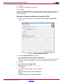
1. Open the JTAG configuration by selecting Xilinx Tools > Configure JTAG Settings
(Figure 17).
X-Ref Target - Figure 17
Figure 17:
JTAG Configuration Settings
2. Select the Digilent USB Cable in Type field
3. Click Automatically Discover Devices on JTAG Chain.
Note: Two workstations are needed when running from the SDK, one for the transmitter and another
for the receiver, because the debugger can only connect to one Digilent USB Cable at a time.
4. Click OK.
5. Select Xilinx Tools > Program FPGA.
Note: Ensure bootloop is used for microblaze_0.
6. Click Program.
7. In the Project Explorer window, right-click and select:
VoIP_TX:
voip_rx_main > Run As > Launch on Hardware
VoIP_RX:
voip_tx_main > Run As > Launch on Hardware
XAPP1194 (v1.1) September 30, 2015
www.xilinx.com
22
Debug
Note: The choice is provided whether to run the software application either from MIG or block RAM by
editing the linker script. The default setting in the linker script is to execute the software application from
block RAM.
Debug
Upon completion of the reference design setup, check these items to ensure proper operation:
Transmitter
•
Ensure that the two LEDs on the two RJ45 ports of the Inrevium TB-FMCL-GLAN-B board
are ON indicating transmission from the board for two links (primary and secondary):
•
LED Right: 1GBASE-TX link/speed
•
LED Left: Transmit activity
•
Ensure that the LEDs (D2, D4, D8 and D9) on the Inrevium TB-FMCH-3GSDI2A board are
OFF indicating there are streams present at the board.
•
Ensure that the user-defined LEDs (GPIO LEDs, item 14, Figure 8, page 14) for port 0, 6
and 7 of the KC705 evaluation kit board are ON:
•
GPIO LED 0: DDR initialization complete
•
GPIO LED 6: 100 MHz Locked
•
GPIO LED 7: 200 MHz Locked
Receiver
Reference
Design
•
Ensure that the LED (right) on the two RJ45 ports of the Inrevium TB-FMCL-GLAN-B
board are ON indicating 1GBASE-TX link/speed for the two links (primary and secondary).
•
Ensure that the RX and Duplex LEDs on the TB-FMCL-GLAN-B board are ON indicating
packets are present. See the TB-FMCL-GLAN-B Hardware User Manual [Ref 7].
•
Ensure that the user-defined LEDs (GPIO LEDs, item 14, Figure 8, page 14) for port 0, 6
and 7 of the KC705 evaluation kit board are ON:
•
GPIO LED 0: DDR initialization complete
•
GPIO LED 6: 100 MHz Locked
•
GPIO LED 7: 200 MHz Locked
The reference design files for this application note can be downloaded from:
https://secure.xilinx.com/webreg/clickthrough.do?cid=352502, registration required.
Table 8 shows the reference design checklist.
Table 8: Reference Design Checklist
Parameter
Description
General
Developer name
Muhammad Ilias, Gilbert Magnaye, Myo Tun
Aung, Josh Poh, Tom Sun
Target devices (stepping level, ES,
production, speed grades)
Kintex-7 XC7K325T-2FFG900
Source code provided
Yes
Source code format
VHDL (some sources are encrypted)
Design uses code/IP from existing Xilinx
application note/reference designs, CORE
Generator™ software, or third party
Yes, core generated from Vivado IP catalog
XAPP1194 (v1.1) September 30, 2015
www.xilinx.com
23
Notes
Table 8: Reference Design Checklist (Cont’d)
Parameter
Description
Simulation
Functional simulation performed
N/A
Timing simulation performed
N/A
Test bench used for functional and timing
simulations
N/A
Test bench format
N/A
Simulator software/version used
N/A
SPICE/IBIS simulations
N/A
Implementation
Synthesis software tools/version used
Vivado 2013.4
Implementation software tools/versions used Vivado 2013.4
Static timing analysis performed
Yes (passing the implementation stage)
Hardware Verification
Notes
Hardware verified
Yes
Hardware platform used for verification
Kintex-7 FPGA KC705 evaluation kit Rev 1.0
and 1.1
Software Application
The software application can be set to run from either DDR (mig_1) or block RAM
(lmb_subsys_ilmb_bram_if_cntlr_lmb_subsys_dlmb_bram_if_cntlr) by properly
setting values in the linker script (lscript.ld).
Video Over IP Receiver
The tready control generator module (tready_ctrl.vhd) is instantiated in the design to
regulate the data ready signal by ensuring that the buffered packets level in the SMPTE
2022-1/2 Video Over IP receiver core is greater or equal to that set in the playout delay register.
Conclusion
This application note describes a video over IP network system using various Xilinx IP cores.
The reference design demonstrates the ability of the SMPTE 2022-1/2 Video Over IP cores to
encapsulate and de-encapsulate multiple transport streams into a TS per IP configuration
(user-configured values) and transport them through a 1 Gb/s Ethernet pipe. The utilization of
the Ethernet bandwidth is over 90% with 125 Mb/s TS Video Streams for each of four channels,
with an FEC size of 4 x 4 with TS per IP of 1 and TS size of 188 bytes. The Reference Design
can perform recovery of a limited number of Ethernet packets when impairment is introduced
into the network with the forward error correction engine turned on.
XAPP1194 (v1.1) September 30, 2015
www.xilinx.com
24
References
References
This application note uses these references:
1. SMPTE 2022-1/2 Video Over IP Core product page
2. Tri-Mode Ethernet MAC Core product page
3. Kintex-7 FPGA KC705 Evaluation Kit product page
4. 7 Series FPGAs Configuration User Guide (UG470)
5. Inrevium TB-FMCH-3GSDI2A 3G/HD/SD 3GSDI FMC Connectivity mezzanine card
product page
6. Inrevium TB-FMCL-GLAN-B 1000 Base-T Ethernet FMC Connectivity mezzanine card
product page
7. TB-FMCL-GLAN-B Hardware User Manual
8. LogiCORE IP SMPTE 2022-1/2 Video Over IP Transmitter v1.0 Product Guide (PG180)
9. LogiCORE IP SMPTE 2022-1/2 Video Over IP Receiver v1.0 Product Guide (PG181)
10. AXI Reference Guide (UG761)
11. 7 Series FPGAs Memory Interface Solutions v2.0 User Guide (UG586)
12. LogiCORE IP Tri-Mode Ethernet MAC Product Guide (PG051)
Revision
History
Notice of
Disclaimer
The following table shows the revision history for this document.
Date
Version
Description of Revisions
09/30/2015
1.1
Updated for Table 4 and VOIP_TX Main Menu Hyperterminal Output
option.
12/18/2013
1.0
Initial Xilinx release.
The information disclosed to you hereunder (the “Materials”) is provided solely for the selection and use of
Xilinx products. To the maximum extent permitted by applicable law: (1) Materials are made available "AS
IS" and with all faults, Xilinx hereby DISCLAIMS ALL WARRANTIES AND CONDITIONS, EXPRESS,
IMPLIED, OR STATUTORY, INCLUDING BUT NOT LIMITED TO WARRANTIES OF
MERCHANTABILITY, NON-INFRINGEMENT, OR FITNESS FOR ANY PARTICULAR PURPOSE; and (2)
Xilinx shall not be liable (whether in contract or tort, including negligence, or under any other theory of
liability) for any loss or damage of any kind or nature related to, arising under, or in connection with, the
Materials (including your use of the Materials), including for any direct, indirect, special, incidental, or
consequential loss or damage (including loss of data, profits, goodwill, or any type of loss or damage
suffered as a result of any action brought by a third party) even if such damage or loss was reasonably
foreseeable or Xilinx had been advised of the possibility of the same. Xilinx assumes no obligation to
correct any errors contained in the Materials or to notify you of updates to the Materials or to product
specifications. You may not reproduce, modify, distribute, or publicly display the Materials without prior
written consent. Certain products are subject to the terms and conditions of the Limited Warranties which
can be viewed at http://www.xilinx.com/warranty.htm; IP cores may be subject to warranty and support
terms contained in a license issued to you by Xilinx. Xilinx products are not designed or intended to be
fail-safe or for use in any application requiring fail-safe performance; you assume sole risk and liability for
use of Xilinx products in Critical Applications: http://www.xilinx.com/warranty.htm#critapps.
XAPP1194 (v1.1) September 30, 2015
www.xilinx.com
25
Automotive Applications Disclaimer
Automotive
Applications
Disclaimer
XILINX PRODUCTS ARE NOT DESIGNED OR INTENDED TO BE FAIL-SAFE, OR FOR USE
IN ANY APPLICATION REQUIRING FAIL-SAFE PERFORMANCE, SUCH AS APPLICATIONS
RELATED TO: (I) THE DEPLOYMENT OF AIRBAGS, (II) CONTROL OF A VEHICLE, UNLESS
THERE IS A FAIL-SAFE OR REDUNDANCY FEATURE (WHICH DOES NOT INCLUDE USE
OF SOFTWARE IN THE XILINX DEVICE TO IMPLEMENT THE REDUNDANCY) AND A
WARNING SIGNAL UPON FAILURE TO THE OPERATOR, OR (III) USES THAT COULD
LEAD TO DEATH OR PERSONAL INJURY. CUSTOMER ASSUMES THE SOLE RISK AND
LIABILITY OF ANY USE OF XILINX PRODUCTS IN SUCH APPLICATIONS.
XAPP1194 (v1.1) September 30, 2015
www.xilinx.com
26