1
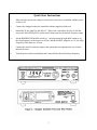
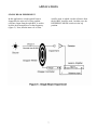
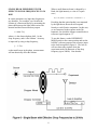
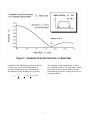
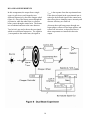
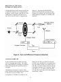
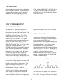
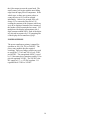
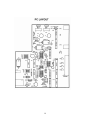
MODEL SR540
OPTICAL CHOPPER
MODEL SR540
OPTICAL CHOPPER
Copyright © 1986, 1988, 1995, 1997
Stanford Research Systems, Inc.
All Rights Reserved
Rev. 2.6 (06/2009)
Stanford Research Systems, Inc.
1290-D Reamwood Ave.
Sunnyvale, CA 94089 USA
(408) 744-9040
TABLE OF CONTENTS
Symbols used ………………………………………………………...……….
2
Specifications ………………………………………………..……………….
3
Safety & Preparation for Use …………………………………..………..
4
Quick Start Instructions …………………………………………………..
5
Operating Instructions
Introduction ……………………………………………………………
6
Frequency of Operation ………………………………………………
6
Changing Blades ……………………………………………………….
6
Baseplate Removal …………………………………………………….
6
Applications
Single Beam …………………………………………………………...
7
Single Beam Chopping to 20 kHz ……………………………………..
8
Dual Beam Experiments ……………………………………………….
10
Detection at Sum & Difference Frequencies …………………………..
11
Variable Aperture ……………………………………………………...
11
Calibration ……………………………………………………………………
12
Circuit Description
Motor Speed Control …………………………………………………..
12
Optical Pick-Offs ………………………………………………………
12
Frequency Synthesis …………………………………………………...
13
Frequency Display ……………………………………………………..
13
Power Supplies ………………………………………………………...
14
Parts List ……………………………………………………………………...
15
PC Layout …………………………...………………………………………..
19
Schematic …………………………...………………………………………...
21
1
2
SPECIFICATIONS
Chop Frequency
4 Hz to 400 Hz with 6 slot blade.
400 Hz to 3.7 kHz with 30 slot blade.
Frequency Stability
250 ppm/°C typical.
Long Term Frequency Drift
< 2%, 100 Hz < f < 3700 Hz
Phase Jitter
0.2° rms from 50 Hz to 400 Hz.
0.5° rms from 400 Hz to 3.7 kHz.
Frequency Display
4 digit, 1 Hz resolution, 1 Hz accuracy.
Frequency Control
10 turn pot with 3 ranges:
4 Hz to 40 Hz
40 Hz to 400 Hz
400 Hz to 3.7 kHz
VCO
0 to 10 VDC. Control voltage overrides frequency dial.
Reference Modes
Switch
up
middle
down
Dimensions
Controller
7.7" x 5.1" x 1.8"
Chopper Head 2.8" x 2.1" x 1.0"
Blade Diameter
4.00"
Power
100 / 120 / 220 / 240 VAC
50 / 60 Hz
12 Watts
Warranty
Electronics - One year parts and labor on materials and
workmanship.
Chopper Motor - Ninety days parts and labor on materials and
workmanship.
Left BNC
ƒinner
5xƒ
ƒ + ƒinner
3
Right BNC
ƒ
ƒ
ƒ – ƒinner
SAFETY AND PREPARATION
************ CAUTION ************
LINE FUSE
This instrument may be damaged if operated
with the LINE VOLTAGE SELECTOR set for
the wrong ac input-source voltage or if the
wrong fuse is installed.
Verify that the correct line fuse is installed
before connecting the line cord. For 100V and
120V, use a 1/4 Amp fuse and for 220V and
240V, use a 1/8 Amp fuse.
LINE VOLTAGE SELECTION
LINE CORD
The SR540 operates from a 100V, 120V, 220V,
or 240V nominal ac power source having a line
frequency of 50 or 60 Hz. Before connecting
the power cord to a power source, verify that the
LINE VOLTAGE SELECTOR card, located in
the rear panel fuse holder, is set so that the
correct ac input voltage value is visible
(figure 1).
This instrument has a detachable, three-wire
power cord with a three-contact plug for
connection to both the power source and
protective ground. The protective ground
contact connects to the accessible metal parts of
the instrument. To prevent electrical shock,
always use a power source outlet that has a
properly grounded protective-ground contact.
To Change Voltage Selected: Open the cover on
the power entry module using a small
screwdriver; pull the voltage selector card
straight out using long-nose pliers; orient
selector card so that the desired voltage is
readable at the bottom; orient the indicator pin
to point up when desired voltage is readable at
the bottom (figure 2); insert voltage selector
card into housing, printed side facing left, and
edge containing desired voltage first; replace
cover and verify that the indicator pin shows the
desired voltage.
OPERATE ONLY WITH COVERS IN
PLACE
To avoid personal injury, do not remove the
product covers or panels. Do not operate the
product without all covers and panels in place.
KEEP HANDS CLEAR OF CHOPPER
BLADE
4
Quick Start Instructions
1.
Make sure the correct line voltage is selected, the correct fuse is installed, and the power
switch is off.
2.
Connect the chopper head to the controller with the supplied coiled cord.
3.
Mount the 30 slot wheel for 400 Hz to 3.7 kHz or the 6 slot wheel for 4 Hz to 400 Hz,
and set the MAX FREQ/SLOT switch on the front panel for the desired frequency range.
4.
Set the REFERENCE MODE switch 'up'. In this position the right BNC output is at ƒ,
the chop frequency of the outer row of slots; and the left BNC output is at ƒinner, the chop
frequency of the inner row of slots.
5.
Connect the lock-in's reference input to the output that corresponds to the row of slots
that will be used.
6.
Turn the power switch on and adjust the 10-turn dial for the desired chop frequency.
5
OPERATING INSTRUCTIONS
of the reference outputs will degrade at
the low end of the range, so switch to the
next lower MAX FREQ / SLOTS range.
INTRODUCTION
The Model SR540 Optical Chopper is used to
square-wave modulate the intensity of optical
signals. The unit can chop light sources at rates
from 4 Hz to 3.7 kHz. Versatile, low jitter
reference outputs provide the synchronizing
signals required for several operating modes:
single or dual beam; sum & difference
frequency; and synthesized chopping to 20 kHz.
5.
FREQUENCY OF OPERATION
The choice of operating frequency is influenced
by several factors:
1.
Avoid low frequency operation (below
100Hz). In general, phase jitter,
background noise and lock-in amplifier
noise all degrade at low frequencies.
2.
Avoid high frequency operation. Motor
lifetime will be reduced if the unit is
operated for extended periods above
2KHz.
3.
Avoid known noise frequencies. For
example, the line frequency and all its
even and odd harmonics should be
carefully avoided.
4.
Always use the correct wheel as
indicated by the MAX FREQ / SLOTS
switch. Using the wrong wheel will
seriously degrade the performance of the
synthesized reference outputs (left
BNC). For frequencies from 4Hz to 400
Hz use the 6/5 slot blade; from 400Hz to
3.7kHz use the 30/25 slot blade.
CHANGING BLADES
The chopper blade (figure 4) may be replaced by
removing the three flat head screws, which hold
the outside hub to the wheel. When replacing
the blade, be sure to insert the blade between the
slotted optical detectors before placing it on the
wheel. Secure the blade by sandwiching it
between the wheel and outer hub. Install and
loosely tighten the three flat head screws, which
hold the hub to the wheel. Then firmly tighten
all three screws. Handle blades carefully as they
are easily bent.
BASEPLATE REMOVAL
The baseplate of the unit may be removed to
allow for pole mounting. Use an allen wrench to
remove the 6-32 bolt from the bottom of the
baseplate.
Avoid using the bottom 10% of the
frequency control dial. The phase jitter
6
APPLICATIONS
SINGLE BEAM EXPERIMENT
In this application, a single optical beam is
chopped by the outer row of slots, and the
reference output from the right BNC is used to
lock the lock-in amplifier to a chop frequency
(figure 5). Note, that the inner row of slots
could be used, in which case the reference from
the left BNC would be used. In either case, the
REFERENCE MODE switch is in the 'up'
position.
7
SINGLE BEAM EXPERIMENT WITH
EFFECTIVE CHOP FREQUENCIES TO 20
KHZ
When a small diameter beam is chopped by a
blade, the light intensity vs. time is a square
wave,
In certain situations very high chop frequencies
are desirable. For example, you can infer the
lifetime of a fluorescent decay by measuring the
phase shift between the light which excites the
material and the fluorescent decay output.
I(t) = Io (sin wt + 1/3 sin 3wt + 1/5 sin 5wt +…).
Providing that the optical media is not saturated
by the light beam, the media will respond
linearly to each Fourier component. In this case,
we are interested in the response at the 5th
harmonic, for which the chopper controller has a
reference signal output at 5ƒ.
τ = tanø / 2πƒ
where ø is the observed phase shift, ƒ is the
chop frequency, and t is the lifetime. Accuracy
is improved by using a chop frequency,
To use this feature, set the REFERENCE
MODE switch to the center position and use the
left BNC reference output as the reference input
to the lock-in amplifier (figure 6). The lock-in
will now detect the response from the
experiment at the 5th harmonic of the chop
frequency (up to 20kHz). Note that the
ƒ ~ 1 / 2πτ
so that small errors in the phase measurement
will not drastically affect the lifetime.
8
amplitude of the 5th harmonic term will depend
on beam size. For a beam with diameter b,
using the 30 slot wheel with a slot aperture L,
the amplitude of the nth harmonic is given by,
an = 4
n2π2
The amplitude of the 5th harmonic vs. beam
size is plotted in figure 7. If your beam is much
larger than 0.5mm, you may wish to pass the
beam through an aperture or bring it to focus at
the chopper blade.
L cos nπ (1 - b/L)
b
2
9
DUAL BEAM EXPERIMENTS
In this arrangement, the output from a single
source is split in two and chopped at two
different frequencies by the same chopper wheel
(figure 8). One of the beams passes through the
experiment, while the other beam, a reference
beam, passes through a control arm. The beams
are recombined and sent to the same detector.
ƒinner is the response from the experimental arm.
If the detected signal in the experimental arm is
ratioed to the detected signal in the control arm,
then effects due to changing source intensity and
detector efficiency are removed.
Also note that each beam passes through one
beam splitter, reflects off one beam splitter, and
reflects off one mirror, so that effects due to
these components are cancelled in the ratio
output.
Two lock-in's are used to detect the two signals
which are at different frequencies. The signal at
ƒ corresponds to the control arm, the signal at
10
DETECTION AT THE SUM &
DIFFERENCE FREQUENCIES
Certain applications require detection at the sum
or difference frequency of two chopped beams.
In figure 9, a source beam is split into two. One
of the beams is chopped by the outer row of
slots on the wheel, the other is chopped by the
inner row. By placing the REFERENCE
MODE switch in the down position, the sum
frequency is available at the left reference BNC
and the difference frequency is available at the
right BNC.
VARIABLE APERTURE
In some situations one must reduce the duty
cycle of a chopped optical beam. This can be
done with the SR540 by mounting two identical
blades and staggering their position relative to
each other.
blade and a 2% duty cycle on the 6 slot blade.
For duty cycles less than 20%, you should select
the "pulse mode" reference level on the lock-in.
Since the ƒ/6 notch is obscured when two blades
are mounted, only the ƒ & 5ƒ reference outputs
will work (ƒinner, ƒsum, and ƒdiff will not work).
You may observe the duty cycle of the chopped
beam on the ƒ output.
The minimum slot aperture is about 0.5mm,
below which the slotted optical detector will fail
to detect the outer row of slots. This
corresponds to a 10%duty cycle on the 30 slot
11
CALIBRATION
Only one adjustment is required to calibrate the
SR540 Chopper Controller. The adjustment pot
located on the rear panel is used to match the
controller to the motor. Mount the 30-slot
blade, and set the MAX FREQ/SLOT switch to
4 kHz. Set the FREQUENCY ADJUST dial to
7.5, and use a small screwdriver to adjust the
MOTOR CAL pot so that the four digit display
shows 3000 ±10 Hz.
CIRCUIT DESCRIPTION
MOTOR SPEED CONTROL
The output of U5, a precision 10.000VDC
reference, is attenuated by P2, the ten-turn
potentiometer, to control the motor speed. The
set voltage can be overridden by a voltage at the
CONTROL VOLTAGE input. The speed
control voltage is buffered by 2/4 of U3, and
attenuated by R8, R9 and R10. U2, a quad
analog switch, selects the attenuation factor to
provide full-scale voltages of 10.0, 5.0 or
0.5VDC per the setting of the MAX
FREQ/SLOTS switch. The 3/4 of U3 is used to
amplify this voltage by about x2.6. The
MOTOR CAL pot, P1, is used to adjust the gain
of this amplifier to compensate for variations
between motors. The output of the amplifier is
buffered by U1 to drive the motor. R4 senses
and limits the motor current to 200mA by
turning on Q1. The 1/4 of U3 feeds-back a
voltage equal to the voltage applied to the motor
minus 4.7 times the voltage across R4. Since
the feedback voltage goes down when current is
increased, the voltage applied to the motor will
go up; hence the output behaves like a negative
resistance connected to a voltage source. The
negative resistance is about R4 x 4.7, ~ 15Ω.
This is just equal to the real resistance of the
cable and motor windings. With this
arrangement, the speed of the motor will not be
affected by load variations, which normally
would change the current and so change the
voltage that is applied to the motor. This
improves frequency stability of the chopper and
improves the linearity of the speed vs. control
voltage characteristic.
OPTICAL PICK-OFFS
There are two slotted optical switches, which
detect slots in the chopper wheel. Each optical
switch uses an infrared LED and a
phototransistor. If the light passes through a slot
to the phototransistor, its collector current will
be several milliamps. The collectors of the
photo transistors are connected together,
summing their currents. The common collector
is held at 3.0VDC by 4/4 of U3. The current is
sensed by R15, so that the output of 4/4 U3 will
swing by 1 volt/mA of collector current.
Radiated noise at the chop frequency is greatly
reduced, as all lines going to the chopper head
are held at constant voltage.
The waveform at pin 14 of U3 looks like this:
The current from one of the optical switches is
just a square wave at the frequency of the outer
row of slots. The outputs from the second photo
12
frequency of the VCO is set by R22. U4
increases the maximum frequency by switching
in R20 or R21 when the 400 Hz or 4KHz ranges
are selected. The output frequency of the VCO
is divided by U18, which is programmed to
divide by 5 or 11 per the setting of the
REFERENCE MODE switch, SW1. To
generate 5f/6, U18 loads 10 when the counter
reaches 15 to divide by 5. In order for the
frequencies at the input of the phase comparator
to be equal, the VCO must run at 5xf/6.
transistor places a pulse on top of every sixth
pulse, per the chopper wheel design. This
second signal provides a signal at f/6, with
known phase, which is used to synthesize other
reference outputs.
Logic signals at f & f/6 are generated by the dual
comparator U6. The 1/2 of U6 compares the
photo current signal to a fixed voltage of about
3.6VDC in order to generate f. The 2/2 of U6
compares the photo current signal to the peak
value of the photo current signal, less two diode
drops. Comparing to the peak voltage
compensates for variations in LED &
phototransistor sensitivity. Both comparators
have about 0.2V of hysteresis to prevent
multiple edges on logic transitions.
The same circuit is used to generate 5f,
however, the multiplexer, U17, selects f (not
f/6) as the input to the phase detector. To
generate 11f/6, the sum frequency, f/6 is
selected as the input to the phase detector, and
U18 is programmed to divide by 11 by
presetting to 4 when the counter reaches 15. In
all cases, the output of the VCO is passed to the
left reference output BNC. This output is
always a square wave.
FREQUENCY SYNTHESIS
The outer row frequency, f, is measured directly
by one of the phototransistors. The difference
between the outer & inner row frequencies, f/6,
is measured by the other phototransistor. The
other frequencies are synthesized from these two
references by a phase-lock loop circuit.
Name
ƒ
5ƒ
ƒinner
ƒsum
ƒdiff
Frequency
ƒ
5ƒ
5ƒ/6
11ƒ/6
ƒ/6
FREQUENCY DISPLAY
The four-digit frequency display always shows
the frequency, f, of the outer row of slots,
independent of the reference mode, which has
been selected. The time base for the counter is a
32,768Hz crystal oscillator, which is sustained
by U10, a hex inverter. U11, a 14-stage binary
counter and the flip-flop 2/2 U14 are used to
divide by 215 to generate a 1.000-second gate.
Description
outer row
5 x outer row
inner row
outer row + inner row
outer row – inner row
The Dual 1:4 Multiplexer, U17, is used to pass f
or f/6 to the right hand reference output BNC
per the setting of the REFERENCE MODE
switch, SW1. U17 also selects f of f/6 as a
source to the PLL frequency synthesizer circuit.
In order to eliminate one-count flicker in the
result, the count latch 1/2 U14, is set by a falling
edge of the wave form which is to be counted.
When the count latch is set, the reset to the time
base counters is released, starting the onesecond-count period. Also, the reset to U15, the
four-decade counter/latch/display driver is
released to begin the count. The count
accumulates for 1 second, when, the falling edge
of the Q output from 2/2 U14 sets 1/2 U13 high.
The Q output of 1/2 U13 stays high for about
1/2 clock period (15µs) asserting the Latch
Enable input on U15 to transfer the counter
contents to the latch for display. Then 1/2 U13
is reset, and 2/2 U13 is clocked high, asserting
To generate 5f/6, the frequency of the inner row
of slots, U17 selects f/6 as the input to the phase
detector of U12, a CMOS phase-lock loop. The
output of the phase detector is filtered by R23,
R24, and C3. The quad analog switch, U4, will
also switch in C2 or C1 if the 400Hz or 40Hz
MAX FREQ/SLOTS ranges are selected at
SW2. The filtered output of the phase detector
controls the VCO frequency. The maximum
13
the Q-bar output to reset the count latch. The
entire count cycle begins with the next falling
edge from the opto pick-off comparator. If the
wheel stops, so there are no more pulses to
count, the reset to U15 will be asserted
indefinitely. After a few seconds, R36 will
charge C13 to assert the Disp Sel to U15,
causing the contents of the counters (which are
zero) to be displayed instead of the contents of
the latches (which contain the last count). U15
multiplexes the display information to the 4
digit common cathode LED. Each of the digits
are selected in sequence by U15 saturating one
of the display driver transistors Q2-Q5.
POWER SUPPLIES
The power transformer primary is tapped for
operation at 100, 120, 220, or 240VAC. The
power entry module does the required
switching. Full wave bridge rectifiers are used
to rectify the 7.5VAC and 30VAC to 8.5VDC
and 40VDC. The unregulated 40VDC is used
by U1 the motor driver transistor, and by U8 to
provide regulated 30VDC. The 30VDC is the
DC supply to U7, a +15VDC regulator. U9
regulates the 8.5VDC to 5.0VDC.
14
SR540 PARTS LIST
Motor and Motor related Parts List
C 15
J2
M1
O1
O2
PC1
R 30
R 33
Z0
Z0
Z0
Z0
Z0
Z0
Z0
Z0
Z0
Z0
Z0
Z0
5-00102-517
1-00030-100
7-00055-700
3-00173-309
3-00173-309
7-00056-701
0-00000-000
0-00000-000
0-00146-025
0-00147-004
0-00150-026
0-00151-055
0-00205-058
0-00222-021
7-00057-720
7-00058-716
7-00059-721
7-00060-721
7-00061-721
7-00062-716
4.7U
4P4C
12VDC
MOC70U2
MOC70U2
SR541
UNDECIDED PART
UNDECIDED PART
6-32X3/8H
1/4-20X1"
4-40X1/4PF
DC-44-4C-6
EPOXY GLUE
6-32X1/4PP
SR540-1
SR540-10
SR540-2
SR540-3
SR540-6
SR540-9
Capacitor, Tantalum, 35V, 20%, Rad
Connector, Misc.
Misc. Parts
Optical Switch
Optical Switch
Printed Circuit Board
Hardware, Misc.
Hardware, Misc.
Screw, Allen Head, HEX HEAD
Knobs
Screw, Black, All Types
Wire, Other
Glue
Screw, Panhead Phillips
Fabricated Part
Chemically Etched Part
Machined Part
Machined Part
Machined Part
Chemically Etched Part
Main Board and Chassis Assembly Parts List
BR1
BR2
C1
C2
C3
C4
C5
C6
C7
C8
C9
C 10
C 11
C 12
C 13
C 14
C 17
C 18
C 19
C 20
CX1
CX2
D1
D2
3-00062-340
3-00062-340
5-00031-520
5-00033-520
5-00192-542
5-00100-517
5-00127-524
5-00128-509
5-00023-529
5-00038-509
0-00772-000
5-00064-513
5-00100-517
5-00030-520
5-00038-509
5-00100-517
5-00023-529
5-00100-517
5-00192-542
5-00064-513
5-00003-501
5-00017-501
3-00004-301
3-00004-301
KBP201G/BR-81D
KBP201G/BR-81D
220U
47U
22U MIN
2.2U
2.2U
470U
.1U
10U
1.5" WIRE
.0047U
2.2U
2200U
10U
2.2U
.1U
2.2U
22U MIN
.0047U
10P
47P
1N4148
1N4148
15
Integrated Circuit (Thru-hole Pkg)
Integrated Circuit (Thru-hole Pkg)
Capacitor, Electrolytic, 16V, 20%, Rad
Capacitor, Electrolytic, 16V, 20%, Rad
Cap, Mini Electrolytic, 50V, 20% Radial
Capacitor, Tantalum, 35V, 20%, Rad
Capacitor, Tantalum, 50V, 20%, Rad
Capacitor, Electrolytic, 50V, 20%, Rad
Cap, Monolythic Ceramic, 50V, 20%, Z5U
Capacitor, Electrolytic, 50V, 20%, Rad
Hardware, Misc.
Capacitor, Mylar/Poly, 50V, 5%, Rad
Capacitor, Tantalum, 35V, 20%, Rad
Capacitor, Electrolytic, 16V, 20%, Rad
Capacitor, Electrolytic, 50V, 20%, Rad
Capacitor, Tantalum, 35V, 20%, Rad
Cap, Monolythic Ceramic, 50V, 20%, Z5U
Capacitor, Tantalum, 35V, 20%, Rad
Cap, Mini Electrolytic, 50V, 20% Radial
Capacitor, Mylar/Poly, 50V, 5%, Rad
Capacitor, Ceramic Disc, 50V, 10%, SL
Capacitor, Ceramic Disc, 50V, 10%, SL
Diode
Diode
SR540 PARTS LIST
D3
D4
DX100
F1
J1
J3
P1
P2
PC1
PC2
Q2
Q3
Q4
Q5
Q6
R2
R3
R4
R5
R6
R7
R8
R9
R 10
R 11
R 12
R 13
R 14
R 15
R 16
R 17
R 18
R 19
R 20
R 21
R 22
R 23
R 24
R 25
R 26
R 28
R 29
R 31
R 32
R 34
R 35
R 36
R 37
3-00001-301
3-00001-301
3-00203-301
6-00002-611
1-00030-100
1-00031-133
4-00271-445
4-00019-443
7-00054-701
7-00558-701
3-01860-325
3-01860-325
3-01860-325
3-01860-325
3-00020-325
4-00273-401
4-00305-401
4-00773-402
4-00031-401
4-00034-401
4-00034-401
4-00188-407
4-00187-407
4-00193-407
4-00061-401
4-00034-401
4-00048-401
4-00078-401
4-00021-401
4-00272-407
4-00188-407
4-00021-401
4-00059-401
4-00614-407
4-00037-401
4-00131-407
4-00094-401
4-00090-401
4-00054-401
4-00035-401
4-00021-401
4-00034-401
4-00032-401
4-00032-401
4-00057-401
4-00057-401
4-00032-401
4-00034-401
1N4001
1N4001
1N5711
.25A 3AG
4P4C
16 PIN SRA
2.0K
20K
SR540
SR540 LED
MPSA13
MPSA13
MPSA13
MPSA13
PN2222
5.6K
4.3K
2.2
100
10K
10K
4.99K
4.53K
499
240K
10K
2.2K
39K
1.0K
221
4.99K
1.0K
22K
174K
11K
1.00M
6.8K
560
200K
10M
1.0K
10K
100K
100K
220
220
100K
10K
16
Diode
Diode
Diode
Fuse
Connector, Misc.
Connector, Male, Right Angle
Pot, Multi-Turn, Side Adjust
Pot, 10-Turn Panel
Printed Circuit Board
Printed Circuit Board
Transistor, TO-92 Package
Transistor, TO-92 Package
Transistor, TO-92 Package
Transistor, TO-92 Package
Transistor, TO-92 Package
Resistor, Carbon Film, 1/4W, 5%
Resistor, Carbon Film, 1/4W, 5%
Resistor, Carbon Comp, 1/2W, 5%
Resistor, Carbon Film, 1/4W, 5%
Resistor, Carbon Film, 1/4W, 5%
Resistor, Carbon Film, 1/4W, 5%
Resistor, Metal Film, 1/8W, 1%, 50PPM
Resistor, Metal Film, 1/8W, 1%, 50PPM
Resistor, Metal Film, 1/8W, 1%, 50PPM
Resistor, Carbon Film, 1/4W, 5%
Resistor, Carbon Film, 1/4W, 5%
Resistor, Carbon Film, 1/4W, 5%
Resistor, Carbon Film, 1/4W, 5%
Resistor, Carbon Film, 1/4W, 5%
Resistor, Metal Film, 1/8W, 1%, 50PPM
Resistor, Metal Film, 1/8W, 1%, 50PPM
Resistor, Carbon Film, 1/4W, 5%
Resistor, Carbon Film, 1/4W, 5%
Resistor, Metal Film, 1/8W, 1%, 50PPM
Resistor, Carbon Film, 1/4W, 5%
Resistor, Metal Film, 1/8W, 1%, 50PPM
Resistor, Carbon Film, 1/4W, 5%
Resistor, Carbon Film, 1/4W, 5%
Resistor, Carbon Film, 1/4W, 5%
Resistor, Carbon Film, 1/4W, 5%
Resistor, Carbon Film, 1/4W, 5%
Resistor, Carbon Film, 1/4W, 5%
Resistor, Carbon Film, 1/4W, 5%
Resistor, Carbon Film, 1/4W, 5%
Resistor, Carbon Film, 1/4W, 5%
Resistor, Carbon Film, 1/4W, 5%
Resistor, Carbon Film, 1/4W, 5%
Resistor, Carbon Film, 1/4W, 5%
SR540 PARTS LIST
R 38
R 39
R 40
R 41
R 42
R 43
R 44
R 45
R 99
R 100
SW1
SW2
T1
TH100
U1
U2
U3
U4
U5
U6
U7
U8
U9
U 10
U 11
U 12
U 13
U 14
U 15
U 17
U 18
XT1
Z0
Z0
Z0
Z0
Z0
Z0
Z0
Z0
Z0
Z0
Z0
Z0
Z0
Z0
Z0
Z0
4-00034-401
4-00273-401
4-00024-401
4-00031-401
4-00021-401
4-00059-401
4-00021-401
4-00022-401
4-00081-401
4-00355-435
2-00012-206
2-00012-206
6-00014-610
4-00766-431
3-00257-329
3-00074-340
3-00098-340
3-00074-340
3-00188-340
3-00143-340
3-00114-329
3-00149-329
3-00112-329
3-00051-340
3-00169-340
3-00072-340
3-00048-340
3-00048-340
3-00170-340
3-00166-340
3-00171-340
6-00015-620
0-00002-008
0-00009-000
0-00025-005
0-00048-011
0-00089-033
0-00103-040
0-00127-050
0-00128-053
0-00129-053
0-00134-053
0-00149-020
0-00153-057
0-00155-002
0-00185-021
0-00207-003
0-00209-021
10K
5.6K
1.2K
100
1.0K
22K
1.0K
1.0M
470
56V/500A
SPDT
SPDT
SR540
RXE030
TIP41B
CD4066
LM324
CD4066
LH0070-0H
LM393
7815
LM317T
7805
74HCU04
74HC4020
CD4046
74HC73
74HC73
74C926
74HC153
74HC191
32.768 KHZ
2607
FOOT
3/8"
6-32 KEP
4"
3/8X3/32
4" #18 RED
4" #24
5" #24
7-1/4" #24
4-40X1/4PF
GROMMET2
6VM4S
6-32X3/8PP
TO-5
4-40X3/8PP
17
Resistor, Carbon Film, 1/4W, 5%
Resistor, Carbon Film, 1/4W, 5%
Resistor, Carbon Film, 1/4W, 5%
Resistor, Carbon Film, 1/4W, 5%
Resistor, Carbon Film, 1/4W, 5%
Resistor, Carbon Film, 1/4W, 5%
Resistor, Carbon Film, 1/4W, 5%
Resistor, Carbon Film, 1/4W, 5%
Resistor, Carbon Film, 1/4W, 5%
Varistor, Zinc Oxide Nonlinear Resistor
Switch, On-Off-On, Toggle,Right Angle
Switch, On-Off-On, Toggle,Right Angle
Transformer
Thermistor, various
Voltage Reg., TO-220 (TAB) Package
Integrated Circuit (Thru-hole Pkg)
Integrated Circuit (Thru-hole Pkg)
Integrated Circuit (Thru-hole Pkg)
Integrated Circuit (Thru-hole Pkg)
Integrated Circuit (Thru-hole Pkg)
Voltage Reg., TO-220 (TAB) Package
Voltage Reg., TO-220 (TAB) Package
Voltage Reg., TO-220 (TAB) Package
Integrated Circuit (Thru-hole Pkg)
Integrated Circuit (Thru-hole Pkg)
Integrated Circuit (Thru-hole Pkg)
Integrated Circuit (Thru-hole Pkg)
Integrated Circuit (Thru-hole Pkg)
Integrated Circuit (Thru-hole Pkg)
Integrated Circuit (Thru-hole Pkg)
Integrated Circuit (Thru-hole Pkg)
Crystal
Dial
Hardware, Misc.
Lugs
Nut, Kep
Tie
Washer, Flat
Wire #18 UL1007 Stripped 3/8x3/8 No Tin
Wire #24 UL1007 Strip 1/4x1/4 Tin
Wire #24 UL1007 Strip 1/4x1/4 Tin
Wire #24 UL1007 Strip 1/4x1/4 Tin
Screw, Flathead Phillips
Grommet
Power Entry Hardware
Screw, Panhead Phillips
Insulators
Screw, Panhead Phillips
SR540 PARTS LIST
Z0
Z0
Z0
Z0
Z0
Z0
Z0
Z0
Z0
Z0
Z0
0-00222-021
0-00238-026
0-00447-007
0-00524-048
0-00594-050
1-00003-120
1-00053-172
3-00556-340
7-00064-720
7-00065-720
7-00066-709
6-32X1/4PP
6-32X1/4PF
TO-220
8-1/4" #18
4-1/2" #18 BLUE
BNC
USA
HDSP-5323
SR540-7
SR540-8
SR540-11
18
Screw, Panhead Phillips
Screw, Black, All Types
Heat Sinks
Wire, #18 UL1015 Strip 3/8 x 3/8 No Tin
Wire #18 UL1007 Stripped 3/8x3/8 No Tin
Connector, BNC
Line Cord
Integrated Circuit (Thru-hole Pkg)
Fabricated Part
Fabricated Part
Lexan Overlay
19
20