1
Right choice for ultimate yield
LSIS strives to maximize customers' profit in gratitude of choosing us for your partner.
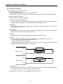
Programmable Logic Controller
XBC Standard/Economic Type Main Unit
XGT Series
User’s Manual
XBC-DR10E
XBC-DR14E
XBC-DR20E
XBC-DR30E
XBC-DN20S
XBC-DN30S
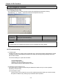
z Read
this manual carefully before
installing, wiring, operating, servicing
or inspecting this equipment.
z Keep
this manual within easy reach
for quick reference.
http://eng.lsis.biz
Safety Instruction
Before using the product …
For your safety and effective operation, please read the safety instructions
thoroughly before using the product.
► Safety Instructions should always be observed in order to prevent accident
or risk with the safe and proper use the product.
► Instructions are separated into “Warning” and “Caution”, and the meaning of
the terms is as follows;
Warning
This symbol indicates the possibility of serious injury
or death if some applicable instruction is violated
Caution
This symbol indicates the possibility of slight injury
or damage to products if some applicable instruction
is violated
► The marks displayed on the product and in the user’s manual have the
following meanings.
Be careful! Danger may be expected.
Be careful! Electric shock may occur.
► The user’s manual even after read shall be kept available and accessible to
any user of the product.
Safety Instruction
Safety Instructions when designing
Warning
Please, install protection circuit on the exterior of PLC to protect
the whole control system from any error in external power or PLC
module. Any abnormal output or operation may cause serious problem
in safety of the whole system.
- Install applicable protection unit on the exterior of PLC to protect
the system from physical damage such as emergent stop switch,
protection circuit, the upper/lowest limit switch, forward/reverse
operation interlock circuit, etc.
- If any system error (watch-dog timer error, module installation error,
etc.) is detected during CPU operation in PLC, the whole output is
designed to be turned off and stopped for system safety. However,
in case CPU error if caused on output device itself such as relay or
TR can not be detected, the output may be kept on, which may
cause serious problems. Thus, you are recommended to install an
addition circuit to monitor the output status.
Never connect the overload than rated to the output module nor
allow the output circuit to have a short circuit, which may cause a
fire.
Never let the external power of the output circuit be designed to
be On earlier than PLC power, which may cause abnormal output or
operation.
In case of data exchange between computer or other external
equipment and PLC through communication or any operation of
PLC (e.g. operation mode change), please install interlock in the
sequence program to protect the system from any error. If not, it
may cause abnormal output or operation.
Safety Instruction
Safety Instructions when designing
Caution
I/O signal or communication line shall be wired at least 100mm
away from a high-voltage cable or power line. If not, it may cause
abnormal output or operation.
Safety Instructions when designing
Caution
Use PLC only in the environment specified in PLC manual or
general standard of data sheet. If not, electric shock, fire, abnormal
operation of the product or flames may be caused.
Before installing the module, be sure PLC power is off. If not,
electric shock or damage on the product may be caused.
Be sure that each module of PLC is correctly secured. If the
product is installed loosely or incorrectly, abnormal operation, error or
dropping may be caused.
Be sure that I/O or extension connecter is correctly secured. If
not, electric shock, fire or abnormal operation may be caused.
If lots of vibration is expected in the installation environment,
don’t let PLC directly vibrated. Electric shock, fire or abnormal
operation may be caused.
Don’t let any metallic foreign materials inside the product, which
may cause electric shock, fire or abnormal operation..
Safety Instruction
Safety Instructions when wiring
Warning
Prior to wiring, be sure that power of PLC and external power is
turned off. If not, electric shock or damage on the product may be
caused.
Before PLC system is powered on, be sure that all the covers of
the terminal are securely closed. If not, electric shock may be caused
Caution
Let the wiring installed correctly after checking the voltage rated
of each product and the arrangement of terminals. If not, fire,
electric shock or abnormal operation may be caused.
Secure the screws of terminals tightly with specified torque when
wiring. If the screws of terminals get loose, short circuit, fire or abnormal
operation may be caused.
*
Surely use the ground wire of Class 3 for FG terminals, which is
exclusively used for PLC. If the terminals not grounded correctly,
abnormal operation may be caused.
Don’t let any foreign materials such as wiring waste inside the
module while wiring, which may cause fire, damage on the product
or abnormal operation.
Safety Instruction
Safety Instructions for test-operation or repair
Warning
Don’t touch the terminal when powered. Electric shock or abnormal
operation may occur.
Prior to cleaning or tightening the terminal screws, let all the
external power off including PLC power. If not, electric shock or
abnormal operation may occur.
Don’t let the battery recharged, disassembled, heated, short or
soldered. Heat, explosion or ignition may cause injuries or fire.
Caution
Don’t remove PCB from the module case nor remodel the module.
Fire, electric shock or abnormal operation may occur.
Prior to installing or disassembling the module, let all the external
power off including PLC power. If not, electric shock or abnormal
operation may occur.
Keep any wireless installations or cell phone at least 30cm away
from PLC. If not, abnormal operation may be caused.
Safety Instructions for waste disposal
Caution
Product or battery waste shall be processed as industrial waste.
The waste may discharge toxic materials or explode itself.
Revision History
Version
Date
V 1.0
2010.3
Remark
Page
1. First Edition
-
※ The number of User’s manual is indicated the right side of the back cover.
ⓒ LS Industrial Systems Co., Ltd
2006
All Rights Reserved.
About User’s Manual
About User’s Manual
Congratulations on purchasing PLC of LS Industrial System Co.,Ltd.
Before use, make sure to carefully read and understand the User’s Manual about the functions,
performances, installation and programming of the product you purchased in order for correct use and
importantly, let the end user and maintenance administrator to be provided with the User’s Manual.
The Use’s Manual describes the product. If necessary, you may refer to the following description and order
accordingly. In addition, you may connect our website(http://eng.lsis.biz/) and download the information as a
PDF file.
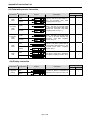
Relevant User’s Manual
Title
XG5000 User’s
Manual
No. of User
Description
Manual
It describes how to use XG5000 software especially about
online functions such as programming, printing, monitoring
10310000512
and debugging by using XGT series products.
XGK/XGB Series
It describes how to use the instructions for programming
Instruction &
using XGK/XGB series.
10310000510
Programming
XGB Analog
User’s Manual
It describes how to use the specification of analog
input/analog
output/temperature
input
module,
system
configuration and built-in PID control for XGB main unit.
XGB Cnet I/F
It describes how to use built-in communication function for
User’s Manual
XGB main unit and external Cnet I/F module.
XGB Fast Ethernet I/F
User’s Manual
10310000920
It describes how to use XGB FEnet I/F module.
10310000816
10310000873
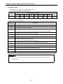
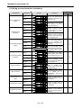
◎
Chapter 1 Introduction
Contents
◎
...................................................................... 1-1~1-5
1.1 Guide to Use This Manual ....................................................................................... 1-1
1.2 Features................................................................................................................... 1-2
1.3 Terminology ............................................................................................................. 1-4
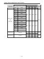
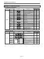
Chapter 2 System Configuration........................................................... 2-1~2-12
2.1 XGB System Configuration .................................................................................... 2-1
2.2 Product List ............................................................................................................ 2-3
2.3 Classification and Type of Product Name .............................................................. 2-5
2.3.1 Classification and type of basic unit .........................................................................2-5
2.3.2 Classification and type of expansion module ...........................................................2-6
2.3.3 Classification and type of special module .................................................................2-7
2.3.4 Classification and type of communication module .....................................................2-8
2.4 System Configuration ............................................................................................. 2-9
2.4.1 Cnet I/F system ..........................................................................................................2-9
2.4.2 Ethernet system........................................................................................................2-12
Chapter 3 General Specifications ................................................................. 3-1
3.1 General Specifications ............................................................................................. 3-1
Chapter 4 CPU Specifications ................................................................. 4-1~4-9
4.1 Performance Specifications ................................................................................... 4-1
4.2 Names of Part and Function .................................................................................. 4-4
4.3 Power Supply Specifications .................................................................................. 4-6
4.4 Calculating Example of Consumption Current/Voltage .......................................... 4-8
4.5 Data Backup Time .................................................................................................. 4-9
Chapter 5 Program Configuration and Operation Method.................. 5-1~5-37
5.1 Program Instruction ................................................................................................ 5-1
5.1.1 Program execution methods ....................................................................................5-1
5.1.2 Operation processing during momentary power failure ...........................................5-2
5.1.3 Scan time ..................................................................................................................5-3
5.1.4 Scan Watchdog timer ...............................................................................................5-5
5.1.5 Timer processing ......................................................................................................5-6
5.1.6 Counter processing ..................................................................................................5-9
5.2 Program Execution ...............................................................................................5-11
5.2.1 Configuration of program ........................................................................................5-11
5.2.2 Program execution methods ....................................................................................5-11
5.2.3 Interrupt . ..................................................................................................................5-13
5.3 Operation Mode ................................................................................................... 5-25
5.3.1 RUN mode ..............................................................................................................5-25
5.3.2 STOP mode ............................................................................................................5-26
5.3.3 DEBUG mode .........................................................................................................5-26
5.3.4 Change operation mode .........................................................................................5-30
5.4 Memory.................................................................................................................. 5-31
5.4.1 Data memory ..........................................................................................................5-31
5.5 Configuration Diagram of Data Memory .............................................................. 5-33
5.5.1 “S” type .....................................................................................................................5-33
5.5.2 “H” type .....................................................................................................................5-34
5.5.3 Data latch area setting..............................................................................................5-35
Chapter 6 CPU Functions ...................................................................... 6-1~6-25
6.1 Type Setting ........................................................................................................... 6-1
6.2 Parameter Setting .................................................................................................. 6-2
6.2.1 Basic parameter setting ............................................................................................6-2
6.2.2 I/O parameter setting ................................................................................................6-3
6.3 Self-diagnosis Function .......................................................................................... 6-4
6.3.1 Saving of error log ....................................................................................................6-4
6.3.2 Troubleshooting ........................................................................................................6-4
6.4 Remote Functions.................................................................................................... 6-6
6.5 Forced Input/Output On and Off Function ............................................................... 6-7
6.5.1 Force I/O setup .........................................................................................................6-7
6.5.2 Processing time and method of Forced Input/Output On and Off ............................6-8
6.6 Direct Input/Output Operation ................................................................................. 6-9
6.7 Diagnosis of External Device ................................................................................ 6-10
6.8 Allocation of Input/Output Number ........................................................................ 6-11
6.9 Online Editing ........................................................................................................ 6-13
6.10 Reading Input/Output Information........................................................................ 6-16
6.11 Monitoring .......................................................................................................... 6-17
6.12 Program Upload Prohibit .................................................................................... 6-22
6.13 Clear All PLC ...................................................................................................... 6-23
6.14 Password Setting per Program Block ................................................................ 6-24
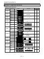
Chapter 7 Input/Output Specifications ............................................... 7-1~7-35
7.1 Introduction ............................................................................................................ 7-1
7.2 Main Unit Digital Input Specifications ..................................................................... 7-7
7.2.1 XBC-DR10E 6 point DC24V input (Source/Sink type)...............................................7-7
7.2.2 XBC-DR14E 8 point DC24V input (Source/Sink type)...............................................7-8
7.2.3 XBC-DR20E 12 point DC24V input (Source/Sink type).............................................7-9
7.2.4 XBC-DR30E 18 point DC24V input (Source/Sink type)...........................................7-10
7.2.5 XBC-DN20S 12 point DC24V input (Source/Sink type)...........................................7-11
7.2.6 XBC-DN30S 18 point DC24V input (Source/Sink type)...........................................7-12
7.3 Main Unit Digital Output Specifications ................................................................ 7-13
7.3.1 XBC-DR10E 4 point relay output .............................................................................7-13
7.3.2 XBC-DR14E 6 point relay output .............................................................................7-14
7.3.3 XBC-DR20E 8 point relay output .............................................................................7-15
7.3.4 XBC-DR30E 12 point relay output ...........................................................................7-16
7.3.5 XBC-DN20S 8 point transistor output (Sink type)....................................................7-17
7.3.6 XBC-DN30S 12 point transistor output (Sink type)..................................................7-18
7.4 Digital Input Module Specifications ...................................................................... 7-19
7.4.1 8 point DC24V input module (Source/Sink type) ....................................................7-19
7.4.2 16 point DC24V input module (Source/Sink type) ..................................................7-20
7.4.3 32 point DC24V input module (Source/Sink type) ...................................................7-21
7.5 Digital Output Module Specifications ................................................................... 7-22
7.5.1 8 point relay output module......................................................................................7-22
7.5.2 16 point relay output module....................................................................................7-23
7.5.3 8 point transistor output module (Sink type) ............................................................7-24
7.5.4 16 point transistor output module (Sink type) ..........................................................7-25
7.5.5 32 point transistor output module (Sink type) ..........................................................7-26
7.5.6 8 point transistor output module (Source type) ........................................................7-27
7.5.7 16 point transistor output module (Source type) ......................................................7-28
7.5.8 32 point transistor output module (Source type) ......................................................7-29
7.6 Combined Digital I/O module Input Specification .................................................. 7-30
7.6.1 8 point DC24V input (Source/Sink type) ..................................................................7-30
7.7 Combined Digital I/O module Output Specification ............................................... 7-31
7.5.18 point relay output....................................................................................................7-31
7.8 IO Wiring by Using Smart Link Board .................................................................. 7-32
7.8.1 Smart link board .......................................................................................................7-32
Chapter 8 Built-in High-speed Counter Function .............................. 8-1~8-54
8.1 High-speed Counter Specifications.......................................................................... 8-1
8.1.1 Performance specifications ......................................................................................8-1
8.1.2 Designation of parts ..................................................................................................8-3
8.1.3 “E” type Functions
..................................................................................................8-6
8.1.4 “S” type Functions
................................................................................................8-23
8.2 Installation and Wiring .......................................................................................... 8-40
8.2.1 Precaution for wiring ...............................................................................................8-40
8.2.2 Example of wiring ...................................................................................................8-40
8.3 Internal Memory ................................................................................................... 8-41
8.3.1 Special area for High-speed counter ......................................................................8-41
8.3.2 Error code ...............................................................................................................8-49
8.4 Examples: Using High-speed Counter ................................................................. 8-50
Chapter 9 Installation and Wiring ........................................................ 9-1~9-18
9.1 Safety Instruction ................................................................................................... 9-1
9.1.1 Fail safe circuit ..........................................................................................................9-3
9.1.2 PLC heat calculation ..................................................................................................9-6
9.2 Attachment/Detachment of Modules ...................................................................... 9-8
9.2.1 Attachment/Detachment of modules
.......................................................................9-8
9.2.2 Caution in handling ..................................................................................................9-13
9.3 Wire ....................................................................................................................... 9-14
9.3.1 Power wiring.............................................................................................................9-14
9.3.2 I/O Device wiring ......................................................................................................9-17
9.3.3 Grounding wiring ......................................................................................................9-17
9.3.4 Specifications of wiring cable ...................................................................................9-18
Chapter 10 Maintenance .................................................................... 10-1~10-2
10.1 Maintenance and Inspection .............................................................................. 10-1
10.2 Daily Inspection .................................................................................................. 10-1
10.3 Periodic Inspection ............................................................................................. 10-2
Chapter 11 Troubleshooting ............................................................ 11-1~11-12
11.1 Basic Procedure of Troubleshooting ...................................................................11-1
11.2 Troubleshooting ....................................................................................................11-1
11.2.1 Troubleshooting flowchart used with when the PWR(Power) LED turns Off. ........11-2
11.2.2 Troubleshooting flowchart used with when the ERR(Error) LED is flickering .......11-3
11.2.3 Troubleshooting flowchart used with when the RUN,STOP LED turns Off. .........11-4
11.2.4 Troubleshooting flowchart used with when the I/O part doesn’t operate normally..11-5
11.3 Troubleshooting Questionnaire ...........................................................................11-7
11.4 Troubleshooting Examples ..................................................................................11-8
11.4.1 Input circuit troubles and corrective actions .........................................................11-8
11.4.2 Output circuit and corrective actions ......................................................................11-9
11.5 Error Code List....................................................................................................11-11
Appendix 1 Flag List ........................................................... App. 1-1~App.1-13
Appendix 1.1 Special Relay (F) List....................................................................... App. 1-1
Appendix 1.2 Communication Relay (L) List.......................................................... App. 1-6
Appendix 2 Dimension............................................................. App.2-1~App.2-4
Appendix 3 Compatibility with MASTER-K ............................ App.3-1~App.3-6
Appendix 4 Instruction List ................................................... App.4-1~App.4-40
Appendix 4.1 Classification of Instructions ............................................................. App.4-1
Appendix 4.2 Basic Instructions ............................................................................ App.4-2
Appendix 4.3 Application Instruction ..................................................................... App.4-5
Appendix 4.4 Special/Communication Instruction............................................... App.4-37
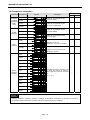
Chapter 1 Introduction
Chapter 1 Introduction
1.1 Guide to Use This Manual
This manual includes specifications, functions and handling instructions for the XGB series PLC.
This manual is divided up into chapters as follows.
No.
Title
Contents
Describes configuration of this manual, unit’s features and
terminology.
Describes available units and system configuration in the XGB
series.
Describes general specifications of units used in the XGB
series.
Chapter 1
Introduction
Chapter 2
System Configurations
Chapter 3
General Specifications
Chapter 4
CPU Specifications
Chapter 5
Program Configuration and
Describes performances, specifications and operations.
Operation Method
Chapter 6
CPU Module Functions
Chapter 7
Input/Output Specifications
Describes operation of basic and input/output.
Chapter 8
Built-in High-speed Counter
Function
Describes built-in high-speed counter functions.
Chapter 9
Installation and Wiring
Describes installation, wiring and handling instructions for
reliability of the PLC system.
Describes the check items and method for long-term normal
operation of the PLC system.
Chapter 10
Maintenance
Chapter 11
Troubleshooting
Describes various operation errors and corrective actions.
Appendix 1
Flag List
Describes the types and contents of various flags.
Appendix 2
Dimension
Shows dimensions of the main units and expansion modules.
Appendix 3
Compatibility with
MASTER-K
Describes the compatibility with MASTER-K.
Appendix 4 Instruction List
Describes the special relay and instruction list.
1-1
Chapter 1 Introduction
1.2 Features
The features of XGB system are as follows.
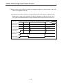
(1) The system secures the following high performances.
(a) High Processing Speed
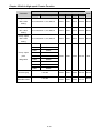
(b) Max. 284 I/O control supporting small & mid-sized system implementation
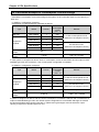
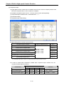
Type
Item
XBC-DRxxE
Reference
XBC-DxxxS
Operation processing
0.24 ㎲ / Step
speed
94ns / Step
-
Max IO contact point
38 points
284 points
In case of using option
module 4 points
(Coming soon)
Program capacity
4kstep
15kstep
Max. no. of expanded Option
stage
stages
module
-
2 7 stages (including option
module 2 stages)
-
(c) Enough program capacity
(d) Expanded applications with the support of floating point.
(e) XBC-DRxxE is expressed as “E” type and XBC-DxxxS is expressed as “S” type.
(2) Compact : the smallest size comparing to the same class model of competitors.
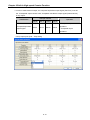
(a) Compact panel realized through the smallest size.
(Unit: mm)
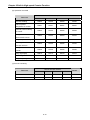
Item
Type
XBC-Dx20S
XBC-Dx30S
Basic unit
XBC-DR10E
XBC-DR14E
XBC-DR20E
XBC-DR30E
Extension module
XBE-,XBF-,XBL-
Reference
Size (W * H * D)
135*90*64
“S” type
100*90*64
“E” type
135*90*64
20 * 90 * 60
Basis of minimum size
(3) Easy attachable/extensible system for improved user convenience.
(a) By adopting a removable terminal block connector (M3 X 6 screw), convenience of wiring may be
increased. (“S” type main unit)
(b) By adopting connector coupling method, modules may be easily connected and separated.
(4) Improved maintenance ability with kinds of register, RTC option, comment backup and etc
(a) Convenient programming environment by providing analogue register and index register.
(b) Improved maintenance ability by operating plural programs and task program through module program.
(c) Built-in Flash ROM enabling permanent backup of program without any separate battery.
(d) Improved maintenance ability by types of comment backup.
(e) Built-in RTC function enabling convenient history and schedule management
1-2
Chapter 1 Introduction
(5) Optimized communication environment.
(a) With max. 2 channels of built-in COM (1 channel for “E” type (except load port)), communication is
available without any expanded of module.
(b) Supporting various protocols to improve the convenience (dedicated, Modbus, user-defined
communication)
(c) Communication module may be additionally increased by adding modules (up to 2 stages such as Cnet,
Enet and etc). (“S” type main unit)
(d) Convenient network-diagnostic function through network & communication frame monitoring.
(e) Convenient networking to upper systems through Enet or Cnet. (“S” type main unit)
(6) Applications expanded with a variety of I/O modules.
(a) 8, 16, 32 points modules provided (if relay output, 8/16 points module).
(b) Single input, single output and combined I/O modules supported.
(7) Applications expanded through analog-dedicated register design and full attachable mechanism.
(a) All analogue modules can be attachable on extension base. (“S” type: up to 7 stages available)
(b) With analog dedicated register(U) and monitoring dedicated function, convenient use for I/O is
maximized (can designate operations using easy programming of U area and monitoring function)
(8) Integrated programming environment
(a) XG 5000: intensified program convenience, diverse monitoring, diagnosis and editing function
(b) XG - PD: COM/network parameters setting, frame monitoring, protocol analysis function
(9) Built-in high speed counter function
(a) Providing High-speed counter 1phase, 2phase and more additional functions.
(b) Providing parameter setting, diverse monitoring and diagnosis function using XG5000.
(c) Monitoring function in XG5000 can inspect without program, inspecting external wiring, data setting and
others.
(10) Built-in position control function (“S” type TR output main unit)
(a) Supporting max 100Kpps 2 axes.
(b) Providing parameter setting, operation data collection, diverse monitoring and diagnosis by using
XG5000.
(c) Commissioning by monitoring of XG5000, without program, inspecting external wiring and operation data
setting.
1-3
Chapter 1 Introduction
(11) Built-in PID (“S” type main unit)
(a) Supporting max. 16 loops.
(b) Setting parameters by using XG5000 and supporting loop status monitoring conveniently with trend
monitor.
(c) Control constant setting through the improved Auto-tuning function.
(d) With many other additional functions including PWM output, ∆MV, ∆PV and SV Ramp, improving the
control preciseness.
(e) Supporting types of control modes such as forward/backward mixed operation, 2-stage SV PID control,
cascade control and etc.
(f) A variety of warning functions such as PV MAX and PV variation warning securing the safety.
1.3 Terminology
The following table gives definition of terms used in this manual.
Terms
Module
Unit
Definition
Remark
Example)
A standard element that has a specified function which configures Expansion module,
the system. Devices such as I/O board, which inserted onto the Special
module,
mother board.
Communication
module
Example)
A single module or group of modules that perform an Main unit,
independent operation as a part of PLC systems.
Expansion unit
PLC System
A system which consists of the PLC and peripheral devices.
A user program can control the system.
-
XG5000
A program and debugging tool for the MASTER-K series.
It executes program creation, edit, compile and debugging.
(PADT: Programming Added Debugging Tool)
-
Software to execute description, edition of basic parameter, high
speed link, P2P parameter, and function of communication
diagnosis
Internal memory area of the CPU module which used to hold I/O
status.
-
Cnet
Computer Network
-
FEnet
Fast Ethernet Network
-
Pnet
Profibus-DP Network
-
Dnet
DeviceNet Network
-
RTC
Abbreviation of ‘Real Time Clock’. It is used to call general IC that
contains clock function.
-
Watchdog Timer
Supervisors the pre-set execution times of programs and warns if
a program is not competed within the pre-set time.
-
XG - PD
I/O image area
1-4
Chapter 1 Introduction
Terms
Definition
Remark
Current flows from the switch to the PLC input terminal if a input
signal turns on.
Z: Input
impedance
Sink Input
−
Current flows from the PLC input terminal to the switch after a
input signal turns on.
Source Input
-
Current flows from the load to the output terminal and the PLC
output turn on.
Sink Output
-
Output
Contact
Current flows from the output terminal to the load and the PLC
output turn on.
Source Output
-
1-5
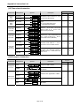
Chapter 2 System Configuration
Chapter 2 System Configuration
The XGB series has suitable to configuration of the basic, computer link and network systems.
This chapter describes the configuration and features of each system.
2.1 XGB System Configuration
XGB series System Configuration is as follows.
For “E” type, only option module can be attached
For “S” type, up to 7 stages connection is available. But in case of attaching 2 option modules, up to 5
stages connection is available. (For communication module, up to 2 connection is available.)
Main Unit
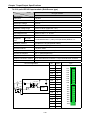
Communication Module
I/O Module
Special Module
Item
Description
• XBC-DxxxS (“S” type): 20~284 points
Total I/O points
• XBC-DRxxE (“E” type): 10~38 points
Digital I/O module
• “S” type: Max. 7
Special module
• “S” type: Max. 7
Maximum number of
Communication
• “S” type: Max. 2
expansion
I/F module
modules
• “S” type: Max. 2
Option module
• “E” type: Max. 2
(In case of 10/14 points, only one is available)
Items
“S” type
• XBC-DR20/30/40/60S • XBC-DN20/30/40/60S
“E” type
• XBC-DR10/14/20/30E
Main unit
2-1
Chapter 2 System Configuration
Item
Description
Digital I/O module
• XBE-DC08/16/32A
• XBE-RY08/16A
• XBE-TN08/16/32A
• XBE-DR16A
• XBE-TP08/16/32A
A/D·D/A module
• XBF-AD04A
• XBF-AH04A
• XBF-RD04A
• XBF-DV04A
• XBF-TC04S
• XBF-AD08A
• XBF-DC04A
• XBF-PD02A
• XBL-C41A
• XBL-EMTA
• XBL-C21A
• XBL-EIMT
• XBL-EIPT
• XBO-DA02A
• XBO-TC02A
• XBO-AH02A
Expansion
module
Communication
I/F module
Digital I/O module
• XBO-DC04A
• XBO-TN04A
Option
Special module
• XBO-AD02A
• XBO-RD01A
module
RTC module
• XBO-RTCA
Memory module
• XBO-M1KB
2-2
Chapter 2 System Configuration
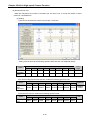
2.2 Product List
XGB series’ product list is as follows.
Expansion Module
Main Unit
Types
Model
Description
Remark
XBC-DR32H
AC100~220V power supply, DC24V input 16 point, Relay output 16 point
-
XBC-DN32H
AC100~220V power supply, DC24V input 16 point, Transistor output 16 point
-
XBC-DR64H
AC100~220V power supply, DC24V input 32 point, Relay output 32 point
-
XBC-DN64H
AC100~220V power supply, DC24V input 32 point, Transistor output 32 point
-
XBC-DR20S
AC100~220V power supply, DC 24V input 12 point, relay output 8 point
XBC-DN20S
AC100~220V power supply, DC24V input 12 point, transistor 8 point
XBC-DR30S
AC100~220V power supply, DC 24V input 18 point, relay output 12 point
XBC-DN30S
AC100~220V power supply, DC 24V input 18 point, transistor output 12 point
XBC-DR40S
AC100~220V power supply, DC 24V input 24 point, relay output 16 point
XBC-DN40S
AC100~220V power supply, DC 24V input 24 point, transistor output 16 point
XBC-DR60S
AC100~220V power supply, DC 24V input 36 point, relay output 24 point
XBC-DN60S
AC100~220V power supply, DC 24V input 36 point, transistor output 24 point
XBC-DR10E
AC100~220V power supply, DC 24V input 6 point, relay output 4 point
XBC-DR14E
AC100~220V power supply, DC 24V input 8 point, relay output 6 point
XBC-DR20E
AC100~220V power supply, DC 24V input 12 point, relay output 8 point
XBC-DR30E
AC100~220V power supply, DC 24V input 18 point, relay output 12 point
Coming soon
Coming soon
Coming soon
XBM-DN16S DC24V Power supply, DC24V Input 8 point, Transistor output 8 point
-
XBM-DN32S DC24V Power supply, DC24V Input 16 point, Transistor output 16 point
-
XBM-DR16S DC24V Power supply, DC24V Input 8 point, Relay output 8 point
-
XBE-DC08A
DC24V Input 8 point
-
XBE-DC16A
DC24V Input 16 point
-
XBE-DC32A
DC24V Input 32 point
-
XBE-RY08A
Relay output 8 point
-
XBE-RY16A
Relay output 16 point
-
XBE-TN08A
Transistor output 8 point
-
XBE-TN16A
Transistor output 16 point
-
XBE-TN32A
Transistor output 32 point
-
XBE-TN64A
Transistor output 64 point (sink type)
-
XBE-TP16A
Transistor output 16 point (source type)
-
XBE-TP32A
Transistor output 32 point (source type)
-
XBE-DR16A
DC24V Input 8 point, Relay output 8 point
-
2-3
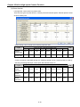
Chapter 2 System Configuration
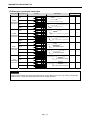
Communication
Module
Special Module
Types
Model
Remark
XBF-AD04A
Current/Voltage input 4 channel
-
XBF-DC04A
Current output 4 channel
-
XBF-DV04A
Voltage output 4 channel
-
XBF-AH04A
Current/voltage input 2 channel, output 2 channel
XBF-RD04A
RTD (Resistance Temperature Detector) input 4 channel
-
XBF-AD08A
Current/voltage input 8 channel
-
XBF-TC04S
TC (Thermocouple) input 4 channel
-
XBF-PD02A
2 axes, line driver type
XBL-C21A
Cnet (RS-232C/Modem) I/F
-
XBL-C41A
Cnet (RS-422/485) I/F
-
XBL-EMTA
Enet I/F
-
XBL-EIMT
RAPIEnet I/F
-
XBL-EIPT
EtherNet/IP module
XBO-M1024
Option
Module
Description
Memory module
XBO-AD02A
Current/voltage input 2channel
XBO-DA02A
Current/voltage output 2 channel
XBO-AH02A
Current/Voltage input 1 channel, output 1 channel
XBO-RD01A
RTD input 1 channel
XBO-TC02A
Thermocouple input 2 channel
XBO-DC04A
DC 24V input 4 point (“S” type HSC 4 channel)
XBO-TN04A
Sink type transistor output 4 channel
(“S” type Positioning 2 axes (low speed))
XBO-RTCA
RTC module
XBO-M1KB
Memory module
2-4
Coming soon
Chapter 2 System Configuration
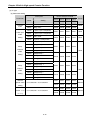
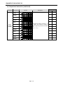
2.3 Classification and Type of Product Name
2.3.1 Classification and type of basic unit
Name of basic unit is classified as follows.
X
B
M
-
D
R
XX
S
XGB PLC economy (E)
XGB PLC standard (S)
XGB PLC
XGB PLC High-end type (H)
No. of IO point
MK language supported (B)
IEC language supported (E)
Relay output (R)
Sink type transistor output (N)
Module type basic unit (M)
Source type transistor output (P)
Compact type basic unit(C)
DC input
Classification
Name
DC input
Relay output
Transistor output
XBM-DR16S
8 point
8 point
None
XBM-DN16S
8 point
None
8 point
XBM-DN32S
16 point
None
16 point
XBC-DR32H
16 point
16 point
None
XBC-DN32H
16 point
None
16 point
XBC-DR64H
32 point
32 point
None
XBC-DN64H
32 point
None
32 point
Compact type
XBC-DN20S
12 point
None
8 point
main nit
XBC-DN30S
18 point
None
12 point
XBC-DR10E
6 point
4 point
None
XBC-DR14E
8 point
6 point
None
XBC-DR20E
12 point
8 point
None
XBC-DR30E
18 point
12 point
None
Modular type
main unit
2-5
Power
DC24V
AC110V~220V
Chapter 2 System Configuration
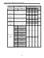
2.3.2 Classification and type of expansion module
Name of expansion module is classified as follows.
X
B
E
-
DC
XX
A
No. of IO point
XGB series
I/O expansion module
Relay output(RY)
Transistor output (TN/TP)
Digital input (DC)
Digital input+ sink type transistor output (DN)
Digital input+ source type transistor output (DP)
Name
DC input
Relay output
Transistor output
XBE-DC08A
8 point
None
None
XBE-DC16A
16 point
None
None
XBE-DC32A
32 point
None
None
XBE-RY08A
None
8 point
None
XBE-RY16A
None
16 point
None
XBE-TN08A
None
None
8 point
XBE-TN16A
None
None
16 point
XBE-TN32A
None
None
32 point
XBE-TP08A
None
None
8 point
XBE-TP16A
None
None
16 point
XBE-TP32A
None
None
32 point
XBE-DR16A
8 point
8 point
None
2-6
Reference
Sink type
Source type
Chapter 2 System Configuration
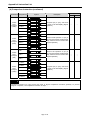
2.3.3 Classification and type of special module
Special module is classified as follows.
X
B
F
-
AD
XX
A
Non-insulation type (A)
Insulation type (S)
XGB series
No. of IO point
Expansion special module
Analog input (AD)
Analog voltage output (DC)
Analog current output (DV)
Voltage, current I/O (AH)
RTD input (RD)
Thermocouple input (TC)
Name
No. of
input ch.
Input type
No. of
output ch.
Output type
XBF-AD04A
4
Voltage/Current
None
-
XBF-AD08A
8
Voltage/Current
None
XBF-DC04A
None
-
4
Current
XBF-DV04A
None
-
4
Voltage
Analog I/O
XBF-AH04A
2
Voltage/Current
2
Voltage/Current
RTD input
XBF-RD04A
4
PT100/JPT100
None
-
TC input
XBF-TC04S
4
K, J, T, R
None
-
Classification
Analog input
Analog output
2-7
Chapter 2 System Configuration
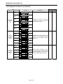
2.3.4 Classification and type of communication module
Name of communication module is classified as follows.
X
B
L
-
C21A
Cnet 1 channel (RS-232C): C21A
XGB series
Cnet 1 channel (RS-422/485): C41A
FEnet 1 port: EMTA
RAPIEnet 1 port: EIMT
Expansion communication module
EtherNet/IP 2 port: EIPT
Classification
Name
Type
XBL-C21A
RS-232C, 1 channel
XBL-C41A
RS-422/485, 1 channel
FEnet Comm. Module
XBL-EMTA
Electricity, open type Ethernet
RAPIEnet Comm. Module
XBL-EIMT
EtherNet/IP Comm. Module
XBL-EIPT
Cnet Comm. Module
Comm. Module between PLCs, electric media,
100 Mbps industrial Ethernet supported
Electricity, open type Ethernet
2-8
Chapter 2 System Configuration
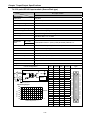
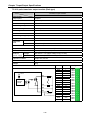
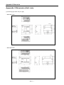
2.4 System Configuration
2.4.1 Cnet I/F system
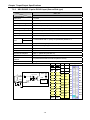
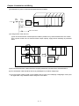
Cnet I/F System is used for communication between the main unit and external devices using RS232C/RS-422 (485) Interface. The XGB series has a built-in RS-232C port, RS-485 port
For “E” type, only one communication port between RS-232C and RS-485 can be used and you can
specify at parameter setting window. For “S” type, RS-232C and RS-485 can be used independently
and add RS-232C dedicated Cnet I/F module (XBL-C21A) and RS-422/485 dedicated Cnet I/F module
(XBL-C41A). It is possible to configure the following communication system on demand
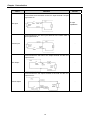
(1) 1:1 communication system
(a) 1:1 communication of an external device (computer) with main unit using a built-in port
(RS-232C/RS-485)
XBC-DN30S
RS-232C / RS-485
(b) 1:1 communication with main unit using a built-in RS-485 port
(In case of built-in RS-232C,it is for connecting to HMI device.)
Built-in RS-485 Connection
XBC-DN30S
PADT
connection
Built-in RS-232C Connection
XP30-TTA
2-9
XBC-DN30S
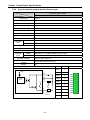
Chapter 2 System Configuration
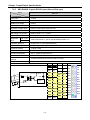
(c) 1:1 RS-232C Communication with remote device via modem by Cnet I/F modules
XBC-DN30S
XBM-DN32S XBL-C21A
XBL-C21A
Modem
Modem
XBC-DN30S
XBL-C21A
Modem
Modem
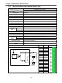
(d) 1:1 communication of an external device (monitoring unit) with main unit using a built-in RS232C/485 port.
XBC-DN30S
XP30-TTA
Built-in RS-232C/485 connection
2-10
Chapter 2 System Configuration
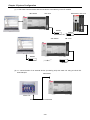
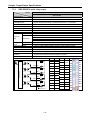
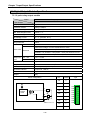
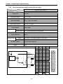
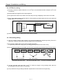
(2) 1:n Communication system
(a) Using RS-485 built-in function can connect between one computer and multiple main units for up
to 32 stations.
XBC-DN30S
XBM-DN32S
XBC-DN30S
PADT
Connection
Max. 32 stations
Built-in RS-232C connection
XBC-DN30S
(b) Using RS-485 built-in function/expansion Cnet I/F module can be connect for up to 32 stations.
Max. 32 stations
XBC-DN30S
XBL-C41A
XBC-DN30S
PADT
connection
Max. 32 stations
Built-in RS-232C connection
Note
1) Refer to ‘XGB Cnet I/F user manual’ for details
2-11
XBL-C41A
Chapter 2 System Configuration
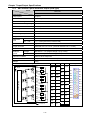
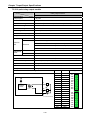
2.4.2 Ethernet system
Ethernet made by cooperation of Xerox, Intel, DEC is standard LAN connection method (IEEE802.3),
which is network connection system using 1.5KB packet with 100Mbps transmission ability. Since
Ethernet can combine a variety of computer by network, it is called as standard specification of LAN and
diverse products. By adopting CSMA/CD method, it is easy to configure the network and collect large
capacity data.
Router or gateway
Hub
Public line
Hub
Router or gateway
H
Hub
Hub
HMI
Note
1) Refer to ‘XGB FEnet I/F user manual’ for details
2-12
HMI
100Base-TX
Chapter 3 General Specifications
Chapter 3 General Specifications
3.1 General Specifications
The General specification of XGB series is as below.
No.
Items
Specification
Reference
1
Ambient Temp.
0 ~ 55 °C
2
Storage Temp.
−25 ~ +70 °C
3
Ambient humidity
5 ~ 95%RH (Non-condensing)
4
Storage humidity
-
5 ~ 95%RH (Non-condensing)
Occasional vibration
Frequency
Vibration
5
-
Acceleration
Amplitude
10 ≤ f < 57Hz
−
0.075mm
57 ≤ f ≤ 150Hz
9.8m/s2 (1G)
−
10 times
resistance
Times
each
Continuous vibration
Frequency
Acceleration
Amplitude
direction
10 ≤ f < 57Hz
−
0.035mm
(X,Y and Z)
57 ≤ f ≤ 150Hz
4.9m/s2 (0.5G)
−
IEC61131-2
2
• Peak acceleration : 147 m/s (15G)
6
Shock resistance
• Duration : 11ms
• Half-sine, 3 times each direction per each axis
Square wave
±1,500 V
impulse noise
Electrostatic
Voltage: 4kV (Contact discharge)
discharge
7
Noise resistance
LSIS standard
Radiated
IEC61000-4-3
field noise
Fast transient
/Burst noise
Segment
Power supply
Digital/Analog Input/Output,
module
Communication Interface
2kV
1kV
Voltage
8
Environment
Free from corrosive gases and excessive dust
9
Altitude
Up to 2,000 ms
10
Pollution degree
2 or less
11
Cooling
Air-cooling
IEC61000-4-2
IEC61131-2,
80 ~ 1,000 MHz, 10V/m
electromagnetic
IEC61131-2
IEC61131-2
IEC61000-4-4
-
Notes
1) IEC (International Electrotechnical Commission):
An international nongovernmental organization which promotes internationally cooperated standardization in
electric/electronic field, publishes international standards and manages applicable estimation system related
with.
2) Pollution degree:
An index indicating pollution degree of the operating environment which decides insulation performance of the
devices. For instance, Pollution degree 2 indicates the state generally that only non-conductive pollution occurs.
However, this state contains temporary conduction due to dew produced.
3-1
Chapter 4 CPU Specifications
Chapter 4 CPU Specifications
4.1 Performance Specifications
The following table shows the general specifications of the XGB module type CPU (XBC-DR10/14/20/30E).
Specifications (“E” type)
Items
XBC-DR10E
XBC-DR14E
XBC-DR20E
XBC-DR30E
Program control method
Reiterative operation, fixed cycle operation, constant scan
I/O control method
Scan synchronous batch processing method (Refresh method),
Directed by program instruction
Program language
Ladder Diagram, Instruction List
Number of Basic
instructions Application
28
677
Processing speed
(Basic instruction)
0.24 ㎲/Step
Program capacity
4 k steps
14 point
Max. I/O points
Main + 1 option
Data area
18 point
28 point
Main + 1 option
Main + 2 options
38 point
-
Main + 2 options
P
P0000 ~ P127F (2,048 point)
M
M0000 ~ M255F (4,096 point)
K
K00000 ~ K2559F (Special area: K2600~2559F) (40,960 point)
L
L00000 ~ L1279F (20,480 point)
F
F000 ~ F255F (4,096 point)
C
100ms, 10ms, 1ms : T000 ~ T255 (256 point)
(Adjustable by parameter setting)
C000 ~ C255 (256 point)
S
S00.00 ~ S127.99
D
D0000 ~ D5119 (5120 word)
U
U00.00 ~ U07.31
(Analog data refresh area: 256 word, analog data refresh area)
Z
Z000~Z127 (128 Word)
T
Remark
Total program
128
Initial task
1
Cyclic task
Max. 8
I/O task
Max. 4
Internal device task
Max. 8
Operation mode
RUN, STOP, DEBUG
Self-diagnosis function
Detects errors of scan time, memory, I/O
Program port
RS-232C (Loader)
Back-up method
Latch area setting in basic parameter
Internal consumption current
250mA
315mA
355mA
485mA
Weight
330g
340g
450g
465 g
Word
-
4- 1
Chapter 4 CPU Specifications
The following table shows the general specifications of the XGB compact type CPU (XBC-DN20/30S).
Specifications (“S” type)
Items
XBC-DN20S
XBC-DR20S
XBC-DN30S
XBC-DR30S
Program control method
Reiterative operation, fixed cycle operation, constant scan
I/O control method
Scan synchronous batch processing method (Refresh method),
Directed by program instruction
Program language
Ladder Diagram, Instruction List
Number of Basic
instructions Application
28
687
Processing speed
(Basic instruction)
94 ns/Step
Program capacity
15 k steps
Max. I/O points
Data area
244 point (Main + Expansion 7 stages)
254 point (Main + Expansion 7 stages)
P
P0000 ~ P1023F (16,384 point)
M
M0000 ~ M1023F (16,384 point)
K
K0000 ~ K4095F (65,536 point)
L
L0000 ~ L2047F (32,768 point)
F
F0000 ~ F1023F (16,384 point)
C
100ms, 10ms, 1ms : T0000 ~ T1023 (1,024 point)
(Adjustable by parameter setting)
C0000 ~ C1023 (1,024)
S
S00.00 ~ S127.99
D
D0000 ~ D10239 (10,240 word)
U
U00.00 ~ U0A.31 (Analog data refresh area: 352 word)
Z
Z000~Z127 (128 Word)
R
R0000~R10239 (10,240 word)
T
Total program
128
Initial task
1
Cyclic task
Max. 8
I/O task
Max. 8
Internal device task
Max. 8
Operation mode
RUN, STOP, DEBUG
Self-diagnosis function
Detects errors of scan time, memory, I/O
Program port
RS-232C 1 channel
Back-up method
Latch area setting in basic parameter
Internal consumption current
Weight
Remark
-
Word
-
240 mA
255 mA
470g
475g
4- 2
Chapter 4 CPU Specifications
Specifications
Items
“E” type
PID control function
Cnet I/F function
“S” type
Remark
Controlled by instructions, Auto-tuning, PWM output,
Supported
Forced output, Adjustable operation scan time, Anti Windup, Delta
MV function, SV-Ramp function
in “S” type
Dedicated protocol support
MODBUS protocol support
User defined protocol support
Select one port between RSRS-232C 1 port, RS-485 1 port
232C 1 port, RS-485 1 port by
respectively
parameter
1 phase: 100 kHz 2 channel, 20kHz 6
Capacity
1 phase: 4 kHz 4 channel
channel
2 phase: 2 kHz 2 channel
2 phase: 50 kHz 1 channel, 8kHz 3
Built-in function
High-speed counter
channel
4 different counter modes according to input pulse and
addition/subtraction method
Counter
mode
Additional
function
Positioning function
Basic function
Positioning
function
• 1 phase pulse input: addition/subtraction counter
• 1 phase pulse input: addition/subtraction counter by B
phase
• 2 phase pulse input: addition/subtraction counter
• 2 phase pulse input:
• 2 phase pulse input:
addition/subtraction
by
addition/subtraction by rising
rising/falling
pulse
phase
pulse phase differences
differences
• Internal/External preset function
• Latch counter function
• Comparison output function
• Revolution number per unit time function
No. of control axis: 2 axes
Control method: position/speed control
Control unit: pulse
Positioning data: 80 data/axis (operation step No. 1~80)
Operation mode: End/Keep/Continuous
Operation method: Single, Repeated operation
Positioning method: Absolute / Incremental
Address range: -2,147,483,648 ~ 2,147,483,647
Speed: Max. 100kpps(setting range 1 ~ 100,000pps)
Acceleration / Deceleration method : trapezoidal method
By Home and DOG (Off)
Return to Origin
By Home and DOG (On)
By DOG
JOG operation
Additional
function
Setting range: 1~100,000 ( High / Low speed)
Inching operation, Speed synchronizing operation, Position
synchronizing operation, linear interpolation operation etc.
10 ㎲ 2 point
50 ㎲
(P0000 ~ P0001)
4 point (P0000 ~ P0003)
50 ㎲ 6 point
(P0002 ~ P0007)
10 ㎲ 2 point
4 point: 50 ㎲
(P0000 ~ P0001)
(P0000 ~ P0003)
50 ㎲ 6 point
(P0002 ~ P0007)
Pulse catch
External interrupt
Input filter
Select among 1,3,5,10,20,70,100 ㎳ (Adjustable)
4- 3
Supported
in “S” type
transistor
output
-
Chapter 4 CPU Specifications
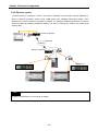
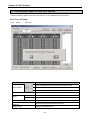
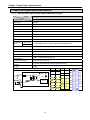
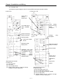
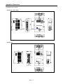
4.2 Names of Part and Function
“E” Type
⑧
③
⑦
①
⑪
⑪
⑥
⑤
⑩
②
No.
⑨
④
Name
Description
①
Input indicator LED
▪ Input indicator LED
②
PADT connecting
connector
▪ PADT connector
RS-232C 1 channel
③
Input terminal block
▪ Input terminal block
④
Output terminal block
⑤
RUN/STOP
switch
⑥
Output indicator LED
▪ Output terminal block
▪ Sets the operation mode of main unit
STOP → RUN: execute operation of program
RUN → STOP: stop operation of program
(In case of STOP, remote mode is available)
▪ Output indicator LED
⑦
⑧
⑨
mode
Status indicator LED
Built-in communication
Connecting connector
Power
supply
connector
⑩
OS mode dip switch
⑪
Option board holder
It indicates CPU module’s status.
▪ PWR(Red on): Power status
▪ RUN(Green on): RUN status
▪ Error(Red flickering): In case of error, it is flickering.
y Built-in RS-232C/485 connecting connector
▪ AC100~240V power supply connector
▪ Dip switch for setting O/S download/Operation mode
On: Boot mode, available to download O/S
Off: User mode, available to download program using PADT
▪For connection option board
4- 4
Chapter 4 CPU Specifications
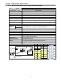
“S” Type
⑧
③
⑦
①
⑥
⑪
⑪
⑤
⑩
②
④
⑨
No.
Name
Description
①
Input indicator LED
▪ Input indicator LED
②
PADT connecting
connector
▪ PADT connector
RS-232C 1 channel
③
Input terminal block
▪ Input terminal block
④
Output terminal block
⑤
RUN/STOP
switch
⑥
Output indicator LED
▪ Output terminal block
▪ Sets the operation mode of main unit
STOP → RUN: execute operation of program
RUN → STOP: stop operation of program
(In case of STOP, remote mode is available)
▪ Output indicator LED
⑦
⑧
⑨
mode
Status indicator LED
Built-in communication
Connecting connector
Power
supply
connector
⑩
OS mode dip switch
⑪
Option board holder
It indicates CPU module’s status.
▪ PWR(Red on): Power status
▪ RUN(Green on): RUN status
▪ Error(Red flickering): In case of error, it is flickering.
y Built-in RS-232C/485 connecting connector
▪ AC100~240V power supply connector
▪ Dip switch for setting O/S download/Operation mode
On: Boot mode, available to download O/S
Off: User mode, available to download program using PADT
▪For connection option board
4- 5
Chapter 4 CPU Specifications
4.3 Power Supply Specifications
It describes the power supply specification of main unit.
Items
XBC-DR10/14E
Rated voltage
(UL warranty voltage)
Input voltage range
Input
AC85~264V(-15%, +10%)
50APeak or less
Input current
0.5A or less (220V), 1A or less (110V)
Permitted momentary
power failure
XBC-DN20/30S
AC 100 ~ 240 V
Inrush current
Efficiency
Output
Specification
XBC-DR20/30E
65% or more
Less than 10 ㎳
Rated
DC5V
500mA
800mA
1.5A
output
DC24V
0.2A
0.2A
0.3A
Output voltage ripple
Power supply status indication
DC5V (±2%)
LED On when power supply is normal
Cable specification
0.75 ~ 2 mm2
* Use the power supply which has 4 A or more fuse for protecting power supply.
4- 6
Chapter 4 CPU Specifications
1) Consumption current (DC 5V)
Type
Main unit
Expansion I/O module
Expansion special module
Expansion communication module
Model
Consumption current (Unit : ㎃)
XBM-DR16S
400
XBM-DN16S
250
XBM-DN32S
280
XBC-DR32H
660
XBC-DR64H
1,040
XBC-DN32H
260
XBC-DN64H
330
XBC-DN30S
255
XBC-DN20S
240
XBC-DR30E
485
XBC-DR20E
355
XBC-DR14E
315
XBC-DR10E
250
XBE-DC32A
50
XBE-DC16A
30
XBE-DC08A
20
XBE-RY16A
440
XBE-RY08A
240
XBE-TN32A
80
XBE-TN16A
50
XBE-TN08A
40
XBE-DR16A
250
XBF-AD04A
120
XBF-AD08A
105
XBF-AH04A
120
XBF-DV04A
110
XBF-DC04A
110
XBF-RD04A
100
XBF-TC04S
100
XBF-PD02A
500
XBL-C21A
110
XBL-C41A
110
XBL-EMTA
190
4- 7
Chapter 4 CPU Specifications
4.4 Calculation Example of Consumption Current/Voltage
Calculate the consumption current and configure the system not to exceed the output current capacity of
basic unit.
(1) XGB PLC configuration example 1
Consumption of current/voltage is calculated as follows.
Type
Model
Unit No.
Internal 5V
consumption
current
Remark
(Unit : ㎃)
Main unit
Expansion
module
XBC-DN20S
1
240
XBE-DC32A
2
50
XBE-TN32A
2
80
XBF-AD04A
1
120
XBF-DC04A
1
110
XBL-C21A
1
110
Consumption
current
Consumption
voltage
850 ㎃
In case contact points are On.
(Maximum consumption current)
All channel is used.
(Maximum consumption current)
-
4.25 W
0.85 * 5V = 4.25W
In case system is configured as above, since 5V consumption current is total 850mA and 5V output of XGB
standard type main unit is maximum 1.5A, normal system configuration is available.
(2) XGB PLC configuration example 2
Type
Model
Unit No.
Internal 5V
consumption
current
Remark
(Unit : ㎃)
Main unit
Expansion
module
Consumption
current
Consumption
voltage
XBC-DN30S
1
255
XBE-DR16A
2
250
XBE-RY16A
2
440
XBF-AD04A
2
120
XBL-C21A
1
110
1,985 ㎃
In case all contact points are On.
(Maximum consumption current)
All channel is used.
(Maximum consumption current)
1.985ⅹ 5V = 9.925W
9.925 W
If system is configured as above, total 5V current consumption is exceeded 1,985 mA and it exceeds the 5V
output of XGB standard type main unit. Normal system configuration is not available. Although we assume
the above example that all contact points are on, please use high-end type main unit which 5V output
capacity is higher than standard type main unit.
4- 8
Chapter 4 CPU Specifications
(3) XGB PLC configuration example 3
Type
Model
Unit No.
Internal 5V
consumption
current
Remark
(Unit : ㎃)
Main unit
Expansion
module
XBC-DN32H
1
260
XBE-DR16A
2
250
XBE-RY16A
2
440
XBF-AD04A
2
120
XBL-C21A
1
110
Consumption
current
Consumption
voltage
In case of all contact points are
On.
(Maximum consumption current)
All channel is used.
(Maximum consumption current)
1,990 ㎃
1.99A ⅹ 5V = 9.95W
9.95 W
The above system is an example using XBC-DN32H about system example (2). Unlike (2) example, 5V
output capacity of XBC-DN32H is maximum 2A, normal configuration is available.
4.5 Data Backup Time
When RTC module is not installed with main unit, data is kept by super capacitor. Data backup time is
1,000 hours or above at normal temperature. But charge super capacitor enough while power is on over
30 minute.
In case super capacitor is not charged enough or power is off more than data backup time, latch data is
not kept and warning occurs. At this time, phenomenon and measure are as follows.
(1) Phenomenon
(a) RUN mode
1) In case of Remote Run mode, operation mode changes to Stop mode. In case of Local Run
mode, it operates normally with abnormal data backup warning
2) In case of Stop mode, abnormal data backup warning occurs.
(b) Latch data
1) Latch area 1,2 : all data are cleared into “0”.
2) K area, F area : all data are cleared into “0”.
(2) Measure
(a) In case abnormal data backup warning occurs when turning off and turning on within short time
(about 1,000 hours at normal temperature), A/S of main unit is necessary. Be careful data backup
time is getting shorter at high temperature. (About 150 hours at 55℃)
Notice
Above data backup time can be different according to temperature condition.
4- 9
Chapter 5 Program Configuration and Operation Method
Chapter 5 Program Configuration and Operation Method
5.1 Program Instruction
5.1.1 Program execution methods
(1) Cyclic operation method (Scan)
This is a basic program proceeding method of PLC that performs the operation repeatedly for the prepared
program from the beginning to the last step, which is called ‘program scan’. The series of processing like
this is called ‘cyclic operation method’. The processing is divided per stage as below.
Stage
Processing description
-
Start
Initialization processing
Input image area refresh
y A stage to start the scan processing which is executed once
when power is applied or Reset is executed, as below.
I/O module reset
Self-diagnosis execution
Data clear
Address allocation of I/O module and type register
y If initializing task is designated, Initializing program is executed.
y Reads the state of input module and saves it in input image
area before starting the operation of program.
Program operation processing
Program start
y Performs the operation in order from the program start to last
step.
Program last step
Output image area refresh
END
y Performs the operation in order from the program start to last step.
y A processing stage to return to the first step after CPU module
completes 1 scan processing and the processing performed is as
below.
Update the current value of timer and counter etc.
User event, data trace service
Self-diagnosis
High speed link, P2P e-Service
Check the state of key switch for mode setting
5-1
Chapter 5 Program Configuration and Operation Method
(2) Interrupt operation (Cycle time, Internal device)
This is the method that stops the program operation in proceeding temporarily and carries out the
operation processing which corresponds to interrupt program immediately in case that there occurs the
status to process emergently during PLC program execution.
The signal to inform this kind of urgent status to CPU module is called ‘interrupt signal’. There is a Cycle
time signal that operates program every appointed time and external interrupt signal that operates program
by external contact (“S” type: P000~P007, “E” type: P000~P003). Besides, there is an internal device start
program that starts according to the state change of device assigned inside.
(3) Constant Scan (Fixed Period)
This is the operation method that performs the scan program every appointed time. This stands by for a
while after performing all the scan program, and starts again the program scan when it reaches to the
appointed time. The difference from constant program is the update of input/output and the thing to
perform with synchronization.
At constant operation, the scan time indicates the net program processing time where the standby time is
deducted. In case that scan time is bigger than ‘constant’, [F0005C] ‘_CONSTANT_ER’ flag shall be ‘ON’.
5.1.2 Operation processing during momentary power failure
CPU module detects the momentary power failure when input power voltage supplied to power module is
lower than the standard. If CPU module detects the momentary power failure , it carries out the operation
processing as follows.
If momentary power failure within 10 ms is occurred, main unit (CPU) keeps the operation. But, if
momentary power failure above 10 ㎳, the operation is stop and the output is Off. Restart processing
like at power input shall be performed.
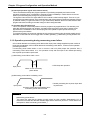
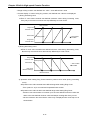
(1) Momentary power failure within 10 ms
y CPU keeps the operation.
Input power
Within 10 ms momentary
power failure
(2) Momentary power failure exceeding 10 ms
y Restart processing like at power input shall
be performed.
Input power
Momentary power failure exceeding 20ms
momentary power failure exceed
Remark
1) Momentary power failure?
This means the state that the voltage of supply power at power condition designated by PLC is
lowered as it exceeds the allowable variable range and the short time (some ms ~ some dozens ms)
interruption is called ‘momentary power failure’ ).
5-2
Chapter 5 Program Configuration and Operation Method
5.1.3 Scan time
The processing time from program step 0 to the next step 0 is called ‘Scan Time’.
(1) Scan time calculation expression
Scan time is the sum of the processing time of scan program and interrupt program prepared by the user
and PLC internal time, and is distinguished by the following formula.
(a) Scan time = Scan program processing time + Interrupt program processing time + PLC internal
processing time
y Scan program processing time = processing time of user program except interrupt program
y Interrupt program processing time = Sum of interrupt program proceeding time processed during 1 scan
y PLC internal processing time = Self-diagnosis time + I/O refresh time + Internal data processing time
+ Communication service processing time
(b) Scan time depends on whether to execute interrupt program and communication processing.
Type
“E” type
“S” type
MPU processing time
Executing
PLC internal
ladder
processing
(4Kstep)
time
5.4 ㎳
1.0 ㎳
3.0 ㎳
Expansion interface processing time
Comm. module
Digital I/O module
Analog module
(main/expansion)
(32 point, 1 unit)
(8 channel, 1 unit)
(200 byte, 1 block)
0.5 ㎳
0.5 ㎳
0.3 ㎳
3.0 ㎳
0.8 ㎳
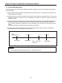
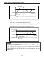
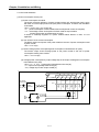
The main unit executes controls along the following steps. A user can estimate the control performance of a
system that the user is to structure from the following calculation.
③I/O data Refresh
④Network Service
②System check &
Task processing
⑤ XG5000 Service
Program
Scan
①Ladder
Ladder Scan
Scan
Output
Input
Expansion
Module
Interface
Ladder Scan
Network Module
Data exchange
I/O Module
Data Refresh
Scan time = ① Scan program process + ② System check & Task process + ③I/O data Refresh
+ ④ Network Service + ⑤ XG5000 Service + ⑥ User Task Program process
① Scan program process = no. of instruction x process speed per each instruction (refer to XGK/XGB
instruction user manual)
② System check & Task process: 600 ㎲ ~ 1.0 ms [varies depending on the usage of auxiliary functions]
③XG5000 Service process time: 100 ㎲ at the max data monitor
④ Task Program process time: sum of task processing time that occurs within a scan; the time calculation
by task programs are as same as that of scan program.
5- 3
Chapter 5 Program Configuration and Operation Method
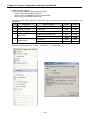
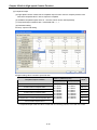
(2) Example
The scan time of a system consisting of main unit (program 4kstep) + five 32-point I/O modules + one analog
module + one communication modules (200 byte 1 block)
Scan time(㎲) = ladder execution time + system processing time + digital module I/O processing time +
analog I/O processing time + communication module processing time + XG5000 Service processing time
= (2047 x (0.67(LOAD)+ 0.80(OUT)) + (500) + (300 x 5) + (3000 x 1) + (800 x 1) + (100) ㎲
= 3009 + 500 + 1500 + 3000 + 800 + 100 ㎲ = 8909 ㎲
= 8.9 ㎳
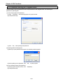
(But, in case of online editing or writing XG-PD parameter, scan time increases temporary up to 100ms)
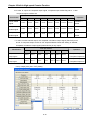
(3) Scan time monitor
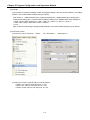
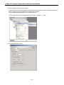
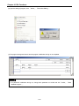
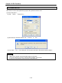
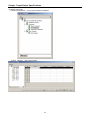
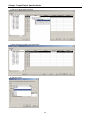
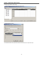
(a) Scan time can be monitored 『Online』-『PLC Information』-『Performance』.
(b) Scan time is save in special relay (F) area as follows.
y F0050: max. value of scan time (unit: 0.1 ms)
y F0051: min. value of scan time (unit: 0.1 ms)
y F0052: current value of scan time (unit: 0.1 ms)
5- 4
Chapter 5 Program Configuration and Operation Method
5.1.4 Scan Watchdog timer
WDT (Watchdog Timer) is the function to detect the program congestion by the error of hardware and software of
PLC CPU module.
(1) WDT is the timer used to detect the operation delay by user program error. The detection time of WDT is set
in Basic parameter of XG5000.
(2) If WDT detects the excess of detection setting time while watching the elapsed time of scan during
operation, it stops the operation of PLC immediately and keeps or clears the output according to
parameter setting
(3) If the excess of Scan Watchdog Time is expected in the program processing of specific part while performing
the user program (FOR ~ NEXT instruction, CALL instruction), clear the timer by using ‘WDT’ instruction.
‘WDT’ instruction initializes the elapsed time of Scan Watchdog Timer and starts the time measurement from
0 again.
(For further information of WDT instruction, please refer to Instruction.)
(4) To clear the error state of watchdog, we can use the following method : power re-supply, manipulation of
manual reset switch, mode conversion to STOP mode.
WDT
count(ms)0 1 2 3 …..
WDT Reset
…8 9 0 1 2 …
SCAN END
012…
WDT instruction
execution
Remark
1) The setting range of Watchdog Timer is 10 ~ 1000ms (Unit: 1ms).
5- 5
…6 7 0 1 2 …
SCAN END
Chapter 5 Program Configuration and Operation Method
5.1.5 Timer processing
The XGB series use up count timer. There are 5 timer instructions such as on-delay (TON), off-delay (TOFF),
integral (TMR), monostable (TMON), and re-triggerable (TRTG) timer.
The measuring range of 100msec timer is 0.1 ~ 6553.5 seconds, 10msec timer is 0.01 ~ 655.35 seconds,
and that of 1msec timer is 0.001 ~ 65.53 seconds. Please refer to the ‘XG5000 User manual’ for details.
Preset value
Timer output relay
Timer type
(1) On delay timer
The current value of timer starts to increase from 0 when the input condition of TON instruction turns on.
When the current value reaches the preset value (Current value=Preset value), the timer output relay
(Txxxx) turns on. When the timer input condition is turned off, the current value becomes 0 and the timer
output relay is turned off.
Input condition
t0
t1
t2
t5
t4
t3
Output relay
t0+PT
t5
t4+PT
t1
Preset value
Current value
t1
t0
t2
t3
t4
t5
(2) Off delay timer
The current value of timer set as preset value and the timer output relay is turned on when the input
condition of TOFF instruction turns on. When the input condition is turned off, the current value starts to
decrease. The timer output relay is turned off when the current value reaches 0.
Input condition
t0
t2
t1
t3
t5
Output relay
t0
t1+PT
t2
t5+PT
Preset value
Current value
t0
t1
t2
5- 6
t4
t5
Chapter 5 Program Configuration and Operation Method
(3) Integral timer
In general, its operation is same as on-delay timer. Only the difference is the current value will not be clear
when the input condition of TMR instruction is turned off. It keeps the elapsed value and restart to
increase when the input condition is turned on again. When the current value reaches preset value, the
timer output relay is turned on.
The current value can be cleared by the RST instruction only.
Timer input
condition
t0 t1
t2
t5
t4
Timer output relay
PT = (t1-t0)+(t3-t2)
Preset value
Current value
t0
t1
t2
t3
t5
t5+PT
Timer reset input
(4) Monostable timer
In general, its operation is same as off-delay timer. However, the change of input condition is ignored
while the timer is operating (decreasing). When current value reaches preset value the timer output relay
is turned off and current value is cleared.
Timer input
condition
t0
t2
t1
t4
t3
Timer output relay
t0
t2
t0+PT
t2+PT
t4
Preset value
Current value
t0
t1
t2
5- 7
t4
t4+PT
Chapter 5 Program Configuration and Operation Method
(5) Retriggerable timer
The operation of retriggerable timer is same as that of monostable timer. Only difference is that the
retriggerable timer is not ignore the input condition of TRTG instruction while the timer is operating
(decreasing). The current value of retriggerable timer will be set as preset value whenever the input
condition of TRTG instruction is turned on.
Timer input condition
t3
Timer output relay
t2
Preset value (PV)
Current value (ET)
t0
t3
t0+PT
Remark
The Maximum timer error of timers of XGB series is ‘1 scan time + the time from 0 step to timer
instruction’
5- 8
Chapter 5 Program Configuration and Operation Method
5.1.6 Counter processing
The counter counts the rising edges of pulses driving its input signal and counts once only when the input
signal is switched from off to on. XGB series have 4 counter instructions such as CTU, CTD, CTUD, and
CTR. The followings shows brief information for counter operation. Refer to the ‘XGB Instruction Manual’ for
details.
• Up counter increases the current value.
• Down counter decreases the current value.
• Up/Down counter compares the input value from both counters input.
• Ring counter increase the current value and the current value is cleared as 0 when the current value
reaches the preset value.
(1) Renewal of counter’s current value and contact On/Off
(a) Up counter
• Up counter increases the current value at the rising edges of input.
• The counter output contact (Cxxx) is turned On when the current value reaches the preset value.
When the reset input is turned On, the counter output contact (Cxxx) is turned Off.
(b) Down counter
• Down counter decreases the current value at the rising edges of input.
• The counter output contact (Cxxx) is turned On when the current value reaches the preset value.
When the reset input is turned On, the counter output contact (Cxxx) is turned Off.
(c) Up/Down counter
• The current value is increased with the rising edge of up-count input signal, and decreased with the
rising edge of down-count input signal. The counter output contact (Cxxx) is turned On when the
current value is same as or more than current value. The counter output contact (Cxxx) is turned Off
when the current value is same as or less than current value.
• When the reset input is turned On, the current value is cleared as 0.
5- 9
Chapter 5 Program Configuration and Operation Method
(d) Ring counter
• The current value is increased with the rising edge of the counter input signal, and the counter output
contact (Cxxx) is turned on when the current value reaches the preset value. Then the current value and
counter output contact (Cxxx) is cleared as 0 when the next rising edge of the counter input signal is
applied.
• When the reset input is turned On, the counter output contact is cleared as 0.
(2) Maximum counting speed
The maximum counting speed of determined by the length of scan time. Counting is possible only when
the on/off switching time of the counter input signal is longer than scan time.
C max =
Maximum counting speed
n
1
×( )
100 tS
n : duty (%)
t S : scan time [s]
• Duty is the ratio of the input signal’s on time to off time as a percentage.
On
Off
Off
T1
T2
T1 ≤ T2, n =
T1 > T2, n =
x 100 [%]
T2
x 100 [%]
T1+T2
Remark
1) Use of High Speed Counter
In order to counter pulse that is faster than maximum counting speed of normal counter, use
built-in High Speed counter function.
5- 10
Chapter 5 Program Configuration and Operation Method
5.2 Program Execution
5.2.1 Configuration of program
All functional elements need to execute a certain control process are called as a ‘program’. Program is stored in
the built-in RAM mounted on a CPU module or flash memory of a external memory module. The following table
shows the classification of the program.
Program type
Description
Initializing program
• It will be executed till the specific Flag ‘INIT_DONE’ is on. And while the
initialization task is executed, cycle task, external interrupt task and internal
device task are not executed. I/O refresh, high speed counter and
communication are executed
Scan program
• The scan program is executed regularly in every scan.
Cycle time interrupt
program
• The program is performed according to the fixed time interval in case that the
required processing time condition is as below.
In case that the faster processing than 1 scan average processing time is
required
In case that the longer time interval than 1 scan average processing time is
required
In case that program is processed with the appointed time interval
External interrupt
program
• The external interrupt program is performed process on external interrupt
signal.
Subroutine
program
• Only when some condition is satisfied.(in case that input condition of CALL
instruction is On)
5.2.2 Program execution methods
Here describes the program proceeding method that is executed when the power is applied or key switch is ‘RUN’.
The program performs the operation processing according to the configuration as below.
Start processing
It executes up to execution of INIT_DONE instruction when initializing program is designated.
Initializing program
Subroutine program
External interrupt program
Scan program
Cycle time program
END processing
5- 11
Only when some
condition is satisfied.
Chapter 5 Program Configuration and Operation Method
(1) Scan program
(a) Function
• This program performs the operation repeatedly from 0 step to last step in order prepared by the program
to process the signal that is repeatedly regularly every scan.
• In case that the execution condition of interrupt by task interrupt or interrupt module while executing
program is established, stop the current program in execution and perform the related interrupt program.
(2) Interrupt program
(a) Function
• This program stops the operation of scan program and then processes the related function in prior to
process the internal/external signal occurred periodically/non-periodically.
(b) Type
• Task program is divided as below.
▶ Cycle time task program: available to use up to 8.
▶ Internal device task program: available to use up to 8.
▶ I/O (External contact task program): “S” type available to use up to 8. (P000 ~ P007)
“E” type available to use up to 4. (P000~P003)
• Cycle time task program
▶ Performs the program according to the fixed time internal.
• Internal device task program
▶ Performs the corresponding program when the start condition of internal device occurs.
▶ The start condition detection of device shall be performed after processing of scan program.
• I/O (External contact task program)
▶ Performs the program according to the input external signal (“S” type: P000~P007, “E” type:
P000~P003).
Remark
(1) Write the interrupt program as shortly as possible. In case same interrupt occurs repeatedly
before completion of interrupt, program is not executed and O/S watch dog error may occur.
(2) Though interrupt which has lower priority occurs many times during execution of interrupt
which has higher priority, interrupt which has lower priority occurs only one time.
5- 12
Chapter 5 Program Configuration and Operation Method
5.2.3 Interrupt
For your understanding of Interrupt function, here describes program setting method of XG5000 which is an XGB
programming S/W. Example of interrupt setting is as shown bellows.
• Interrupt setting
Interrupt source
Interrupt name
priority
Task No.
Program
Initializing
Interrupt 0_
-
-
-
Cycle time 1
Interrupt 1_cycle time
2
0
Cycle time 1
External
Interrupt 2_external
2
8
External
Internal device
Interrupt 3_internal
3
14
Internal
Cycle time 2
Interrupt 4_cycle time
3
1
Cycle time 2
Scan program
Initializing
(Before INIT_DONE instruction)
Interrupt 1_Cycle time
occur
Cycle time 1/
external occur
simultaneously
Cycle time 1 execution
Cycle time 1 execution
External I/O execution
Internal device
Interrupt occur
Cycle time 2
occur
Cycle time 2 execution
END
Internal device interrupt
execution
Cycle time 1
execution
Timed-driven 1
execution
Remark
• In case that several tasks to be executed are waiting, execute from the highest Task Program in
priority. When the same priority tasks are waiting, execute from the order occurred.
• While interrupt executing, if the highest interrupt is occurred, the highest interrupt is executed earliest of
all.
• When power On, All interrupts are in the state ‘Enable’. In case you don’t use it, disable the
interrupts by using DI instruction. If you want to use it again, enable by using EI instruction.
• Internal device interrupt is executed after END instruction.
5- 13
Chapter 5 Program Configuration and Operation Method
(1) How to prepare interrupt program
Generate the task in the project window of XG5000 as below and add the program to be performed by each
task. For further information, please refer to XG5000 user’s manual.
(It can be additional when XG5000 is not connected with PLC.)
(a) Click right button of mouse on project name and click 『Add item』-『Task』.
(b) The screen of Task setting is shown. Click 『Initialization』 in Execution condition and make a Task
name.
5- 14
Chapter 5 Program Configuration and Operation Method
(c) Click right button of mouse at registered task and select『Add Item』-『Program』.
(d) Make initializing program. In initializing program, INIT_DONE instruction must be made. If not, Scan
program is not executed.
5- 15
Chapter 5 Program Configuration and Operation Method
(2) How to prepare Cycle interrupt program
Generate the task in the project window of XG5000 as below and add the program to be performed by each
task. For further information, please refer to XG5000 user’s manual.
(It can be additional when XG5000 is not connected with PLC)
(a) Click right button of mouse at registered task and select『Add Item』-『Task』.
• It shows setting screen of Task.
5- 16
Chapter 5 Program Configuration and Operation Method
(b) Task type
Classification
Description
Task name
Make Task name.
Priority
Set the priority of task. (2~7)
Task number
Set the Task number.
• Cycle time task (0 ~ 7): 8
• External I/O task (8 ~ 15): “S” type: 8,
“E” type: 4
• Internal device task (16 ~ 23): 8
Execution
condition
Initialization
Set the initial program when running the project.
Cycle time
Set the cyclic interrupt.
I/O
Set the external I/O.
Internal
device
Set the internal device to interrupt execution.
• Bit: Among Rising, Falling, Transition, On, Off
• Word: Among >,>=,<,<=
Remark
Character, number
available
“2” is the highest
priority number.
-
Till the execution of
INIT_DONE
instruction
0~4294967295 ㎳
available
P000 ~ P007
available
(c) Click right button of mouse at registered task and select『Add Item』-『Program』.
5- 17
-
Chapter 5 Program Configuration and Operation Method
(d) Register the Program name and Program description.
(e) It is displayed the program window to write task program.
(f) It is displayed the setting in project window.
5- 18
Chapter 5 Program Configuration and Operation Method
(3) Task type
Task type and function is as follows.
Type
Spec.
Max. Task
number
I/O task
(Interrupt task)
Cycle time task
(Interval task)
Internal device task
(Single task)
“S” type
“E” type
8
4
8
Rising or falling
edge of main
unit’s contact
P000 ~P003
8
Start condition
Cyclic
(setting up to max.
4,294,967.295 sec. by
1ms unit)
Rising or falling
edge of main
unit’s contact
P000 ~P007
Detection and
execution
Cyclic execution per
setting time
Immediate execution at the edge of
main unit’s contact
Retrieve the condition
and execute after
completing Scan
Program
Detection delay
time
Max. 1 ms delay
Max. 0.05 ms delay
Delay as much as max.
scan time
Execution
priority
2~7 level setting
(2 level is highest in
priority)
2~7 level setting
(2 level is highest in priority)
2~7 level setting
(2 level is highest in
priority)
Task no.
Within 0~7 range
without user
duplication
With 8~15 range without user
duplication
Within 16~23 range
without user duplication
Internal device
execution condition
(4) Processing methods of task program
Here describes common processing method and notices for Task program.
(a) Feature of task program
1) Task Program is executed only when execution condition occurs without every scan repeat processing.
When preparing Task Program, please consider this point.
2) For example, if a timer and counter were used in cyclic task program of 10 second cycle, this timer
occurs the tolerance of max. 10 seconds and the counter and the timer and as the counter checks the
input status of counter per 10 seconds, the input changed within 10 seconds is not counted up.
(b) Execution priority
1) In case that several tasks to be executed are waiting, execute from the highest Task Program in priority.
When the same priority tasks are waiting, execute from the order occurred.
2) In case Cycle time task and external I/O task is occurred concurrently, execute from the highest task
program. (In sequence of XG5000 setting)
3) The task program priority should be set considering the program features, importance and the
emergency when the execution requested.
(c) Processing delay time
There are some causes for Task Program processing delay as below. Please consider this when task
setting or program preparation.
1) Task detection delay (Refer to detailed description of each task.)
2) Program proceeding delay caused by Priority Task Program proceeding
(d) Relationship of initialize, Scan Program and Task Program
1) ser identification task does not start while performing Initialization Task Program.
2) As Scan Program is set as lowest priority, if task occurs, stop Scan Program and process Task Program
in advance. Accordingly, if task occurs frequently during 1 scan or concentrates intermittently, scan time
may extend abnormally. Cares should be taken in case of task condition setting.
5- 19
Chapter 5 Program Configuration and Operation Method
(e) Protection of Program in execution from Task Program
1) In case that the continuity of program execution is interrupted by high priority Task Program during
program execution, it is available to prohibit the execution of Task Program partially for the part in
problem. In this case, it is available to perform the program protection by ‘ DI (Task Program Start
Disabled) and ‘EI (Task Program Start Enabled)’ application instruction.
2) Insert ‘DI’ application instruction in the start position of the part requiring the protection and insert ‘EI’
application instruction in the position to release. Initialization Task is not influenced by ‘DI’, ‘EI’
application instruction.
3) If interrupt is occurred while ‘CALLP’ instruction executing, interrupt program is executed after ‘CALLP’
instruction execution.
(5) Cyclic task program processing method
Here describes the processing method in case that task (start condition) of Task program is set as Cycle
time.
(a) Items to be set in Task
Set the execution cycle and priority which are the start condition o f Task program to execution. Check the
task no. to manage the task.
(b) Cyclic task processing
Performance the corresponding cyclic task program per setting time interval (execution cycle).
(c) Notice in using cyclic task program
1) When cyclic task program is in execution currently or waiting for execution, if the demand to execute the
same task program occurs, the new occurred task shall be disregarded.
2) Timer that makes a demand to execute cyclic task program only while operation mode is Run mode,
shall be added. The shutdown time shall be all disregarded.
3) When setting the execution cycle of cyclic task program, consider the possibility that the demand to
execute several cyclic task program at the same time occurs.
If 4 cyclic task programs that the cycle is 2sec, 4sec, 10sec and 20sec are used, 4 demands of
execution per 20 seconds shall be occurred at the same time and scan time may extend
instantaneously.
5- 20
Chapter 5 Program Configuration and Operation Method
(6) I/O task program processing
It described the I/O task program processing. (“S” type: P000~P007, “E” type: P000~P003)
(a) Items to be set in Task
Set the execution condition and priority to the task being executed. Check the task no. to manage the task.
(b) I/O task processing
If interrupt signal from external signal (I/O) is occurred on main unit (“S” type: P000 ~ P007. “E” type:
P000~P003), task program is executed by external (I/O) signal.
(c) Precaution in using I/O task program
1) If task program which is executed by interrupt signal is on execution or standby status, new task
program which is requested by identical I/O is ignored.
2) Only operation mode is Run mode, execution request of task program is recognized. Namely, execution
request of task program is ignored when operation mode is Stop mode.
5- 21
Chapter 5 Program Configuration and Operation Method
(7) Internal device task program processing
Here describes the processing method of international device task program which extended the task (start
condition) of task program from contact point to device as execution range.
(a) Items to be set in Task
Set the execution condition and priority to the task being executed. Check the task no. for task
management.
(b) Internal device task processing
After completing the scan program execution in CPU module, if the condition that becomes the start
condition of internal device task program is met, according to the priority, it shall be executed.
(c) Precautions in using internal device task program
1) Accordingly, even if the execution condition of internal device task program occurs in Scan Program
or Task Program (Cycle time, I/O), it shall not be executed immediately but executed at the time of
completion of Scan Program.
2) If the demand to execute Internal Device Task Program occurs, the execution condition shall be
examined at the time of completion of Scan Program. Accordingly, if the execution condition of Internal
Device Task occurs by Scan Program or Task Program (Cycle time) during ‘1 scan’ and disappears, the
task shall not be executed as it is not possible to detect the execution at the time of examination of
execution condition.
5- 22
Chapter 5 Program Configuration and Operation Method
(8) Verification of task program
(a) Is the task setting proper?
If task occurs frequently more than needed or several tasks occur in one scan at the same time, scan time
may lengthen or be irregular. In case not possible to change the task setting, verify max. scan time.
(b) Is the priority of task arranged well?
The low priority task program shall be delayed by the high priority task program, which results in disabling
the processing within the correct time and even task collision may occur as next task occurs in the state
that the execution of previous task is delayed. Consider the emergency of task and execution time etc
when setting the priority.
(c) Is the Task Program written in shortest?
If the execution time of Task Program is longer, scan time may lengthen or be irregular. Even it may cause
the collision of task program. Write the execution time as short as possible. (Especially, when writing the
cyclic task program, write the execution time so that the task program can be executed within 10% cycle of
the shortest task among several tasks.)
(d) Is program protection for the high priority task needed during program execution?
If other task is inserted during task program execution, complete the task in execution and operate the
standby tasks in the order of high priority. In case that it is not allowed to insert other task in Scan Program,
prevent the insert partially by using ‘DI’ and ‘EI’ application instruction. The problem may occur while
processing the global variables used commonly with other program or special or communication module.
(9) Program configuration and processing example
If task and program are registered as below.
Interrupt type
Interrupt name
Priority
Task No.
Program
Cycle time
10 ㎳_cycle time
3
0
Program 1
Internal device
Internal device_M00
5
16
Program 2
I/O
I/O_P00
2
8
Program 3
1) Scan program name: “ Scan Program”
2) Execution time respective program: Scan program = 17 ㎳, Program 1 = 2 ㎳, Program 2= 7 ㎳,
Program 3 = 2 ㎳
5- 23
Chapter 5 Program Configuration and Operation Method
Scan started
(Initial operation started)
Scan program stopped New scan started
Scan program
Program 1
10ms_Cycle time
Program 2
Internal device_M000
Program 3
External I/O_P000
Time
0
6 7 8 10 12
20 22 24 25
30 32 34
Process per time
Process
Time (㎳)
0
0~6
6~8
8~10
Scan started and scan program started to execute.
Scan program is executed.
Scan program is stop because execution external I/O (P000) is requested. And program
3 is executed. Request of execution at 7[ms] is ignored because program 3 has been
executing.
Program 3 is finished and Scan program is continued.
20~22
Scan program is stop by request of ‘10 ㎳_Cycle time’ interrupt signal and execute program
1.
Program 1 is finished and Scan program is continued.
Request of ‘Cycle time’ interrupt signal and ‘External I/O (P000)’ signal is occurred
concurrently but priority of ‘External I/O’ signal is higher than ‘Cycle time’ interrupt signal
so program 3 is executed and program 1 is standby.
Program 3 is finished and Scan program is continued.
22~24
After program 3 is completed, program 1 (the program of ‘10ms_Cycle time’ is executed.
24~25
P1 execution completed and the stopped scan program execution finished
10~12
12~20
20
25
25~30
30~32
32~34
34
At the finished point of scan program, check the request of Internal device ‘M000’
execution and execute program 2.
Program P2 is executed.
When ‘10 ㎳_Cycle time’ interrupt signal is occurred, the priority of that is higher than Internal
device ‘M000’ though program 2 is stopped and program 1 is executed.
P1 executed completed and the stopped P2 execution finished
New scan starts (Start scan program execution)
5- 24
Chapter 5 Program Configuration and Operation Method
5.3 Operation Mode
For operation mode of CPU module, there are 3 types such as RUN mode, STOP mode and DEBUG mode..
Here describes the operation processing of each operation mode.
5.3.1 RUN mode
This is the mode to executed program operation normally.
RUN mode first scan start
Initialize data area
Examine Program effectiveness and judge the
possibility of execution
Execute input refresh
Program execute, Interrupt Program execute
Examine the normal operation or missing of
built-in module
Execute output refresh
Communication service and internal processing
RUN mode keep
Operation
mode change
Change to other mode
Operation by changed operation
mode
(1) Processing at mode change
At the beginning, execute initialization of data area and examine the effectiveness of program and judge the
possibility of execution.
(2) Operation processing contents
Execute I/O refresh and program operation.
(a) Detects the start condition of Interrupt Program and executes Interrupt Program.
(b) Examines the normal operation or missing of built-in module.
(c) Communication service and other internal processing.
5- 25
Chapter 5 Program Configuration and Operation Method
5.3.2 STOP mode
This is the mode in stop state without Program operation. It is available to transmit the program through XG5000
only in Remote STOP mode.
(1) Processing at Mode Change
Clear the output image area and execute output refresh.
(2) Operation Processing Contents
(a) Executes I/O refresh.
(b) Examines the normal operation or missing of built-in module.
(c) Communication service or other internal processing.
5.3.3 DEBUG mode (Supported at “S” type)
This is the mode to detect Program error or trace the operation process and the conversion to this mode is
available only in STOP mode. This is the mode to check the program execution state and the contents of each
data and verify the program.
(1) Processing at mode change
(a) Initializes the data area at the beginning of mode change.
(b) Clears the output image area and execute input refresh.
(2) Operation processing contents
(a) Executes I/O refresh.
(b) Debug operation according to setting state.
(c) After finishing Debug operation by the end of Program, execute output refresh.
(d) Examine the normal operation or missing of built-in module.
(e) Executes communication service or other service.
(3) Debug operation
It describes debug mode.
5- 26
Chapter 5 Program Configuration and Operation Method
Item
Start/Stop Debugging
Go
Description
Change the debug ↔ stop mode
It starts debug operation.
Step Over
It operates by 1 step.
Step Into
It starts the subroutine program.
Step Out
It finished the subroutine program.
Go to Cursor
Remark
Other operation is
identical to Step
Over.
Breakpoints List
It operates to current cursor position.
Set/Removes current cursor position to break
points.
It displays list of breakpoints.
Breakpoint Conditions
It specifies device value and number of scan.
Set/Remove Breakpoints
(a) Set/Remove Breakpoints
▪ Sets breakpoint at current cursor position. After breakpoint setting,
displayed.
(b) Go
▪ Run the program to breakpoint. At break-pointer
5- 27
(breakpoint setting indicator) is
(stop indicator) is displayed.
Chapter 5 Program Configuration and Operation Method
(c) Step Over
▪ Run the program to next step. At break point, Step over indicator
is displayed.
(d) Breakpoint List
▪ It displays current Breakpoint List. It supports Select All, Reset All, Goto, Remove, Remove All.
(e) Break condition
▪ It sets Device Break and Scan Break.
5- 28
Chapter 5 Program Configuration and Operation Method
Remark
1) Refer to XG5000 Users Manual ‘Chapter 12 Debugging’ for detailed information.
5- 29
Chapter 5 Program Configuration and Operation Method
5.3.4 Change operation mode
(1) Operation Mode Change Method
The method to change operation mode are as follows.
(a) By mode key of CPU module
(b) By connecting the programming tool (XG5000) to communication port of CPU
(c) By changing the operation mode of other CPU module connected to network by XG5000 connected to
communication port of CPU.
(d) By using XG5000, HMI, computer link module connected to network
(e) By ‘STOP‘ instruction during program execution
(2) Type of operation mode
The operation mode setting is as follows.
Operation mode switch
XG5000 command
Operation mode
RUN
unchangeable
Local Run
RUN
Remote Run
STOP
Remote Stop
Debug
Debug Run
Mode change
Previous operation mode
-
Stop
STOP
RUN -> STOP
(a) Remote mode conversion is available only in the state of ‘Remote Enabled: On’, ‘Mode switch: Stop’.
In case of changing the Remote ‘RUN’ mode to ‘STOP’ by switch, operate the switch as follows.
(STOP) Æ RUN Æ STOP.
Warning
In case of changing Remote RUN mode to RUN mode by switch, PLC operation continues the
operation without interruption.
It is available to modify during RUN in RUN mode by switch but the mode change operation by
XG5000 is limited. This should be set only in case that remote mode change is not allowed.
5- 30
Chapter 5 Program Configuration and Operation Method
5.4 Memory
There are two types of memory in CPU module that the user can use. One is Program Memory that saves the
user program written by the user to build the system, and the other is Data Memory that provides the device area
to save the data during operation.
5.4.1 Data memory
(1) Bit device area
Various Bit Device are provided per function. The indication method is indicated by device type for first digit,
word position by decimal for middle digit and bit position by hexadecimal for the last digit.
Area per device
“E” type
“S” type
Device features
Description
Image area to save the state of I/O device.
After reading the input module state, saves it in the
corresponding P area and sends P area Data
saving the operation result to output module.
P0000 ~
P127f
P0000~
P1023f
M0000 ~
M255f
M0000~
M1023f
Internal device “M”
Internal Memory provided to save Bit Data in
Program
L0000 ~
L1279f
L0000~
L2047f
Communication device
“L”
Device to indicate high speed link/P2P service state
information of communication module.
K00000
~ K2559f
K00000~
K4095f
Preservation device “K”
Device area to preserve the data during power
shutdown, which is used without setting power
shutdown preservation parameter separately. (Pay
attention to write in special area (K2600 ~ 2559F)).
F0000 ~
F255f
F0000~
F1023f
Special device “F”
System flag area that manages the flag necessary
for system operation in PLC.
T0000 ~
T255
T0000~
T1023
Timer device “T”
Area to save the state of contact/current value/set
value of timer device
C0000 ~
C255
C0000~
C1023
Counter device “C”
Area to save the state of contact/current value/set
value of counter device
S00.00 ~
S127.99
S00.00~
S127.99
Step controller “S”
128 x 100 step
Relay for step control
I/O device “P”
5- 31
Chapter 5 Program Configuration and Operation Method
(2) Word device area
Area per device
“E” type
“S” type
Device features
Description
D00000 ~
D5119
D0000~
D10239
Data register “D”
Area to preserve the internal data.
Bit expression possible. (D0000.0)
U00.00 ~
U0A.31
U00.00~
U0A.31
Analog data
register “U”
Register used to read data from special module installed
in the slot. Bit expression possible
Z000 ~
Z127
Z000~
Z127
Index register
“Z”
Dedicated device to use Index function
Bit expression impossible
T0000 ~
T255
T0000~
T1023
Timer current value
register “T”
Area to indicate the current value of timer
C0000 ~
C255
C0000~
C1023
Counter current
value register “C”
Area to indicate the current value of counter
-
R0000~
R10239
File register “R”
Register for saving file
Bit expression available (F0000.0)
5- 32
Chapter 5 Program Configuration and Operation Method
5.5 Configuration Diagram of Data Memory
5.5.1 “E” type
Bit data area
0
P000
P127
M000
M255
K000
K2559
F000
Word data area
~
F
(2048 points)
Auxiliary Relay
D5119
(4096 points)
U00.00
“M”
Keep Relay
(40960 points)
U0A.31
“K”
(4096 points)
“L”
T000
Timer
T255
C000
(256 points)
“T”
S000
S127
(256 points)
“C”
Step controller
(128 x 100 step)
S00.00~S127.99
“S”
Parameter area
“D”
User Program area
(4 K step)
Analog Data
Register
(1024 words)
“U”
Z000
Index Register
Z127
(128 words)
T000
Timer setting value
T255
T000
(256 words)
T255
C000
(256 words)
C255
C000
(256 words)
C255
(256 words)
“Z”
Timer current value
Counter setting value
Counter current value
Counter
C255
FFFF
Data Register
“F”
Link Relay
(20480 points)
~
(5120 words)
“P”
L0000
L1279
0000
I/O Relay
Special Relay
F255
D0000
5- 33
Chapter 5 Program Configuration and Operation Method
5.5.2 “S” type
Bit data area
0
P0000
P1023
M0000
M1023
K0000
K4095
F0000
~
F
D10239
(16384 points)
U00.00
“M”
Keep Relay
(65536 points)
U0A.31
“K”
(16384 points)
“L”
T0000
Timer
T1023
C0000
(1023 points)
“T”
FFFF
Data Register
Parameter area
“D”
(1024 words)
Z000
Index Register
Z127
(128 words)
“U”
“Z”
T0000
Timer setting value
T1023
T0000
(1024 words)
T1023
C0000
(1024 words)
C1023
C0000
(1024 words)
C1023
(1024 words)
Timer current value
Counter setting value
Counter current value
Counter
C1023
S000
S127
(1023 points)
“C”
R0000
File register
(10240 words)
Step controller
(128 x 100 step)
S00.00~S127.99
“S”
User Program area
(15 K step)
Analog Data
Register
“F”
Link Relay
(32768 points)
~
(10240 words)
Auxiliary Relay
L0000
L2047
0000
“P”
Special Relay
F1023
D0000
I/O Relay
(16384 points)
User Program area
Word data area
“R”
R10239
5- 34
Chapter 5 Program Configuration and Operation Method
5.5.3 Data latch area setting
When PLC stops and restarts the data required for operation or the data occurred during operation, if you
want to keep and use those data, data latch can be used and it is available to use a certain area of some
data device as latch area by parameter setting.
The below shows the features for latch device.
Device
1st latch
2nd latch
P
X
X
Image area to save the state of I/O device
M
O
O
Internal device area
K
X
X
Device keeping the device state during power shutdown
F
X
X
System flag area
T
O
O
Timer related area (Bit/words both)
C
O
O
Counter related area (Bit/words both)
S
O
O
Relay for step control
D
O
O
General words data save area
U
X
X
Analog Data Register (latch disabled )
L
X
X
Z
X
X
High speed link/P2P Service state device of communication
module (latch enabled)
Index dedicated Register (latch disabled)
R
O
O
File register (latch enabled)
Features
Remark
▪ K, L, R devices are basically latched.
(1) Latch area setting
(a) Click Device Area Setup of Basic parameter settings.
5- 35
Chapter 5 Program Configuration and Operation Method
(2) Data latch area operation
(a) The method to delete the latched data is as below.
- latch 1, latch 2 clear operation by XG5000
- write by Program (initialization program recommended)
- write ‘0’ FILL from XG5000 monitor mode.
For keep or reset (clear) operation of latch area data according to PLC operation, please refer to the
below table.
No.
Classification
Detailed operation
Latch 1
Latch 2
1
Power change
Off/On
Keep
Keep
2
Reset by XG5000
Overall reset
Reset
Keep
3
Program write (online)
Keep
Keep
4
Data broken
SRAM broken by battery error
Reset
Reset
Data broken by other reason
5
XG5000 online
Clear Latch 1
Reset
Reset
Reset
Keep
Clear Latch 2
Reset
Reset
-
(b) Latch 1 area is cleared by『Online』-『Reset PLC』- “Overall reset”.
5- 36
Chapter 5 Program Configuration and Operation Method
(c) Latch 1, 2 area is cleared by『Online』-『Clear PLC』.
(3) Data initialization
In case of Memory Delete state, the memory of all device shall be cleared as ‘0’. In case of giving the data
value at the beginning according to system, please use the initialization task.
(a) Device area is cleared by click ‘Clear’ in 『Online』-『Clear PLC』-『Clear Memory』.
5- 37
Chapter 6 CPU Functions
Chapter 6 CPU Functions
6.1 Type Setting
It describes setting of XGB PLC type.
PLC
Series
XGB
CPU type
Description
Reference
XGB-DR16C3
Dedicated product
Modular type
XGB-DR32HL
Dedicated product
Modular type
XGB-XBCE
“E” type : XBC-DR10/14/20/30E
Compact type
XGB-XBCH
“H” type : XBC-DR32/64H , XBC-DN32/64H
Compact type
XGB-XBCS
“S” type : XBC-DR20/30S, XBC-DN20/30S
Compact type
XGB-XBMS
“S” type : XBM-DN16/32S , XBM-DR16S
XGB-XECH
“H” type : XEC-DR32/64H, XEC-DN32/64H
Modular type
Compact type
IEC language
Remark
▪ In case type is different, connection is not available.
6- 1
Chapter 6 CPU Functions
6.2 Parameter Setting
This paragraph describes how to set parameters.
6.2.1 Basic parameter setting
Clicking Basic Parameter in the project window shows the following window.
There are three main options ; “Basic Operation Setup” , “Device Area Setup” and “Error Operation
Setup”.
Category
Item
Fixed period
operation
Watchdog timer
Basic
operations
Device
area
Error
operation
Description
Note
Set the time of fixed period operation.
1~999 ㎳
Set the time of scan watchdog.
10~1000 ㎳
Standard input filter
Output during
debugging
Keep output when
an error occurs
Delete all areas
except latch when an
error occurs
Set the time of standard input filter.
Set whether to allow output actually during
debugging operation.
Set whether to preserve output holding
function set in I/O parameter in case of error.
1,3,5,10,20,70,100 ㎳
Select latch area
Set the latch area of each device.
Operation resumes
in case of operation
error
Set whether to pause or resume operation in
case of operation error.
Set whether to clear each device that is not
designated as a latch area in case of error
6- 2
Allowance/Prohibition
Allowance/Prohibition
Allowance/Prohibition
Pause/Resume
Chapter 6 CPU Functions
6.2.2 I/O parameter setting
This setting is to set and reserve each I/O information. Clicking 『I/O Parameter』 in the project
window shows the following setting window.
Clicking 『Module』 in 『Slot Position』 indicates a list of modules, in which you may set I/O
corresponding to the actual system. Then, the following window is displayed.
Clicking 『Details』 in 『Slot Position』 shows the following window to set filter and emergency output.
Remark
(1) If settings are different with I/O module actually accessed, “Inconsistent module type error” occurs,
displaying error.
(2) Without settings, CPU reads each I/O module information and operates.
6- 3
Chapter 6 CPU Functions
6.3 Self-diagnosis Function
6.3.1 Saving of error log
CPU module logs errors occurred so that the causes will be identified and fixed easily. Clicking
『Error/Warning』 of 『Online』 shows the current error and previous error log.
Item
Error/Warning
Error Log
Description
Remarks
Display the current error/warning.
Display a log of error/warning occurred.
Saving up to 100
Remark
(1) Saved data are not deleted until selecting a menu of XG5000 and clicking “Delete”.
6.3.2 Troubleshooting
(1) Trouble types
Trouble occurs due to PLC itself, system configuration error or abnormal operation result detected. Trouble
is divided into trouble mode stopping operation for the safety and warning mode generating alert to user
with a mode in trouble.
The causes troubling PLC system are as follows.
y PLC hardware trouble
y System configuration error
y Operation error while operating user program
y Error detected owing to external device in trouble
(2) Operation mode if trouble occurs
PLC system logs any trouble occurred in flag and determines whether to stop or resume operation
depending on trouble mode.
(a) PLC hardware trouble
In case an error occurs so that PLC such as CPU module and power module may not work normally,
the system is halted, but any warning may not interfere with the operation.
6- 4
Chapter 6 CPU Functions
(b) Operation error while operating user program
Representing an error occurred during operation of user program, in case of numeric operation error,
it displays the error in error flag but the system resumes operating. However, if the operation time
exceeds by the operation monitoring time limit and I/O module does not control it normally, the system
is halted.
(c) Error detected owing to external device in trouble
Representing the detection of external device to be controlled by users program of PLC, if an error is
detected, the system is halted, but any warning may not interfere with the operation.
Remark
(1) If any trouble occurs, the trouble number is saved in a special relay F002,003.
(2) For details of flag, refer to the appendix 1 Flag List.
6- 5
Chapter 6 CPU Functions
6.4 Remote Functions
CPU module may change operation by communication as well as by key switches mounted on the module. To
operate it remotely, it is necessary to set ‘RUN/STOP’ switch to ‘STOP’.
(1) Remote operations are as follows.
(a) Operable by accessing to XG5000 through RS-232C port mounted on CPU module.
(b) Can operate other PLC connected to PLC network with CPU module connected to XG5000.
(2) Remote RUN/STOP
(a) Remote RUN/STOP is the externally controlled RUN/STOP function.
(b) It is convenient when CPU module is located at a position hard to control or when CPU module
within control panel is to control RUN/STOP function remotely.
(3) Remote DEBUG
(a) It manages debugging remotely when remote mode is STOP. Namely, DEBUG operation is to execute
program operation depending on designated operation conditions.
(b) Remote DEBUG is a convenient function when confirming program operation status or data during
system debugging.
(4) Remote Reset
(a) Remote reset is to reset CPU module remotely if an error occurs at a place hard to directly control
CPU module.
(b) Like operation by switches, it supports ‘Reset’ and ‘Overall Reset’.
Remark
(1) For details regarding remote functions, refer to ‘Ch10 Online’ of XG5000 Users Manual.
6- 6
Chapter 6 CPU Functions
6.5 Forced Input/Output On and Off Function
Force I/O function is used to force to turn I/O areas on or off, regardless of program results.
6.5.1 Force I/O setup
Click『 Online 』-『 Force I/O 』.
Item
Description
Move to the beginning and end of I/O area (P000↔P127)
Move address
Move to ±8 of I/O area displayed at the very left.
Move to ±1 of I/O area.
Application
Single
Select All
Delete All
Setting device
Set whether to allow or not Force I/O
Flag
Set whether to allow or not Force I/O by bits.
Data
Set Force I/O data on or off by bits.
Set to allow Force I/O with all I/O area on
Delete to allow Force I/O with all I/O area off.
Display I/O area set as a bit.
6- 7
Chapter 6 CPU Functions
6.5.2 Processing time and processing method of Force Input/Output On and Off
(1) Forced Input
Regarding input, at the time of input refresh it replaces the data of contact set as Force On/Off among
data read from input module with the data as Force and updates input image area. Therefore, user
program executes operations with actual input data while Force input area is operated with data set as
Force.
(2) Forced Output
Regarding output, at the time of output refresh upon the execution user program operation, it replaces
the data of contact set as Force On/Off among data of output image area containing operation results
with data set as Force and outputs the data in output module. Unlike (Force) input, the output image
area is not changed by Force On/Off setting.
(3) Cautions when using Force I/O function
(a) It operates from the time when I/O is individually set as ‘Allow’ after setting Force data.
(b) It is possible to set Force input although I/O module is not actually mounted.
(c) Despite of the power changed Off -> On, operation mode changes or any operation by pressing reset
key, the data of which On/Off is set before is kept in CPU module.
(d) Even in STOP mode, Force I/O data is not removed.
(e) To set new data from the beginning, it is necessary to deselect all settings of I/O by using ‘Delete All’
option.
(4) Operation in case of error
(a) If error occurs after setting forced output, PLC operates based on “Keep output when an error occurs”
in Basic parameter and “Emergency output” in I/O parameter.
If you set “Emergency output” as “Clear” after setting “Keep output when an error occurs”, output is
cleared when an error occurs. If you set “Emergency output” as “Hold” after setting “Keep output when
an error occurs”, output is held when an error occurs.
(b) If you don’t set “Keep output when an error occurs”, output is off when an error occurs.
6- 8
Chapter 6 CPU Functions
6.6 Direct Input/Output Operation
Refreshing I/O operates after completion of scan program. If data of I/O is changed while program is
scanned, it does not refreshed at the changed moment. Refreshed I/O data is applied after ‘END’ instruction
on program.
This function may be useful when directly reading the status of input contact during program operation by
refreshing I/O by means of ‘IORF’ instruction or outputting operation results to output contact.
‘IORF’ command is operated when M00000 is ON. First operand designates slot number. Second operand
designates the upper 32 bit data as mask data. Third operand designates the lower 32 bit data as mask data.
The bit to refresh set as 1 (hFF) and others set as 0 (h00) (not refreshed).
Remark
- When using IORF instruction to read/write data at expansion module, scan time increases by 2ms. So
when executing interrupt task program by external input less than 10ms or cycle time task less than 10ms,
task collision may occurs.
-For details regarding IORF instruction, refer to XGK/XGB Instructions List.
6- 9
Chapter 6 CPU Functions
6.7 Diagnosis of External Device
This flag is provided for a user to diagnose any fault of external device and, in turn, execute halt or warning of
the system. Use of this flag displays faults of external device without any complicated program prepared and
monitors fault location without any specific device (XG5000 and etc) or source program.
(1) Detection and classification of faults in external device
(a) The trouble (fault) of external device may be detected by user program and largely divided, depending
on the type, into error and warning; the former requires halt of PLC operation and the latter simply
displays the status while PLC keeps working.
(b) ‘Error’ uses ‘F202 (_ANC_ERR)’ and ‘Warning’ uses ‘F203 (_ANC_WB) flag’.
(c) As the detection request flag, ’Error’ uses ‘F2002 (_CHK_ANC_ERR) flag’ while ‘Warning’ uses
‘F2003 (_CHK_ANC_WB) flag’.
(2) Troubleshooting external device
(a) When detecting any trouble of external device in user program, it writes a value except ‘0’ by classifying
the type, which is defined by a user in ‘F202 (_ANC_ERR)’ while the detection request flag checks it at
the time when the program ends with ‘F2002 (_CHK_ANC_ERR) On, and PLC outputs based on the
“Emergency Output” setting in I/O parameter, making it as the same error status as detected by PLC
itself.
(b) If any trouble occurs, a user may identify the cause by using XG5000 and alternatively by monitoring
‘F202 (_ANC_ERR) flag’.
Example
M000
FSET
F2020
FSET
F2002
Error device bit On
Error detection request On
(c) If any trouble occurs, CPU is in error status and operation halts. At this moment, F2020 and F2002 flags
are off (error LED switches on and off every second.)
(3) Processing warning of external device
(a) When detecting any warning of external device in user program, it turns on a flag in the warning
position of system flag ‘F203 (_ANC_WB) and if turning on the detection request flag, ‘F2003
(_CHK_ANC_WB)’ , it displays warning at the time when scan program ends. If a warning occurs, the
detection request flag, ‘F2003 (_CHK_ANC_WB)’ is automatically off (F203 is not deleted).
(b) If a warning occurs, the LED switches on and off every other second.
(c) If turning off a bit in question of F203 and turning on F2003 bit after processing warning, warning is
cancelled and the LED turns off.
Example
M000
FSET
F2030
Warning device bit On
FSET
F2003
Warning detection request On
FRST
F2030
Warning cancellation
FSET
F2003
Warning detection request On
M001
6- 10
Chapter 6 CPU Functions
6.8 Allocation of Input/Output Number
Allocation of I/O number is to allocate an address to every I/O of each module to read data from input module
and output data to output module when it executes operations.
XGB series adopts 64 points occupation to every module.
(1) Allocation of I/O number
124 points are allocated to main unit and 64 points are allocated to every module except main unit (incl.
special, communication).
System Configuration
Number of
Connection stage
Type
I/O allocation
Remarks
0
XBC-DN30S
Input : P0000 ~ P003F
Output : P0040 ~ P007F
1
XBE-DC32A
Input : P0080~P011F
Actual input: P0080 ~ P009F
2
XBE-TN32A
Output : P0120 ~ P015F
Actual output : P0120 ~ P013F
3
XBL-C21A
P0160 ~ P019F
-
4
XBF-AD04A
P0200 ~ P023F
-
5
XBF-DV04A
P0240 ~ P027F
-
6
XBE-DC32A
Input : P0280 ~ P031F
Actual input : P0280 ~ P029F
7
XBE-TN32A
Output : P0320 ~ P035F
Actual output : P0320 ~ P033F
Main unit fixed
Empty I/O point is available for internal relay.
(2) In case of allocating IO of IO parameter, allocation information is displayed.
6- 11
Chapter 6 CPU Functions
In case of using monitor function of XG5000, I/O allocation information is displayed.
I/O module allocation
information
Description of each module
6- 12
Chapter 6 CPU Functions
6.9 Online Editing
It is possible to modify program and communication parameter during operation of PLC without control
operation stopped. The following describes basic modification. For details of modifying program, refer to
XG5000 Users Manual.
Items to be modified during operation are as follows.
• Program
• Communication parameter
(1) It displays programs that are currently running.
(2) Click 『Online』-『Start Online Editing』.
6- 13
Chapter 6 CPU Functions
(3) It turns to program modification mode during run when the program background is changed.
(4) Modifying a program.
(5) Upon the modification of program, click 『Online』-『Write Modified Program』.
6- 14
Chapter 6 CPU Functions
(6) Upon the writing of program, click 『Online』-『End Online Editing』.
(7) The program background returns and the program modification during run is completed.
Remark
▪ For parameter modification during run, change each parameter on XG-PD and click『Online』-『Write
Modified Program 』.
6- 15
Chapter 6 CPU Functions
6.10 Reading Input/Output Information
It monitors information of individual modules consisted of XGB series system.
(1) Click『Online』-『I/O Info』. Then, information of each module connected to the system is monitored.
(2) If clicking Details after selecting a module, it displays detail information of a selected module.
6- 16
Chapter 6 CPU Functions
6.11 Monitoring
It monitors system information of XGB series system.
(1) Clicking『Monitor』 displays the following sub-menus.
(2) Items and descriptions
Item
Start/Stop Monitoring
Pause
Resume
Pausing Conditions
Change Current Value
Description
Designate the start and stop of monitor.
Remarks
Click for reverse turn.
Pause monitoring.
-
Resume paused monitor.
-
Pause monitoring if a preset value of device
corresponds to condition.
Change the present value of currently selected
device.
Monitor resumes;
clicking for resume.
-
System Monitoring
Monitor general system information.
-
Device Monitoring
Monitor by device (type).
-
Trend Monitoring
Monitor trend of device set in the system.
Custom Events
Data Traces
Monitor the value of device set when an event set
by a user occurs.
Trace the value of device.
6- 17
For details, refer to
XG5000 Users Manual.
Chapter 6 CPU Functions
(a) Change current value
▪It changes the current value of each device selected in the current program window.
(b) Device monitoring
▪It monitors by device (type).
6- 18
Chapter 6 CPU Functions
(c) Pausing conditions
▪It stops monitoring in case a device value set in the program corresponds.
(d) Trend monitoring
▪It displays device values graphically.
6- 19
Chapter 6 CPU Functions
(e) Custom events
1) It monitors detail information when an event set by a user occurs. Additional user event may be
registered.
2) It sets basic setting and relative device.
If rising edge of M0000 device occurs, it records the message of an alarm, “Out of order Water Tank 1”
and the device values of D0000,L0000,D0100,N1000 are recorded.
3) Set the relative device(s).
6- 20
Chapter 6 CPU Functions
4) Monitor event history of custom event.
5) Double-clicking a number produced monitors the relative values of device and the detail message as
follows.
Remark
▪For details of monitor, refer to XG5000 Users Manual.
6- 21
Chapter 6 CPU Functions
6.12
Program Upload Prohibit
Program Upload Prohibit function prohibits from uploading comment, parameter, program saved on PLC. If
Program Upload Prohibit function is set, you can’t open from PLC, read PLC and compare PLC.
(1) How to set
(a) Click 『Online』-『Write』
(b) Select “Program Upload Prohibit” and click OK.
(2) When reading PLC is prohibited, if you try to read PLC, the following dialog box appears. After releasing
Program Upload Prohibit, execute reading.
(3) How to release Program Upload Prohibit
(a) Click 『Online』-『Write』.
(b) Release Program Upload Prohibit and click OK.
6- 22
Chapter 6 CPU Functions
6.13 Clear All PLC
Clear All PLC function clears parameter, program, data, password saved on PLC
(1) How to clear all PLC
(a) Click 『Online』-『Clear All PLC』.
(b) After selection connection method, click 『Connect』 or 『OK』.
(c) If you select 『Yes』 on the dialog box, PLC program, parameter, data, password will be deleted.
Note
•Clear All PLC function can be executed though not connected.
•If you use Clear All PLC function, password will be deleted. So be careful.
•In case you lose password, use this function to clear password.
6- 23
Chapter 6 CPU Functions
6.14 Password Setting per Program Block
Password Setting per Program Block function sets password for each program block. You should input
password to open program.
(1) How to set program block password
(a) Click 『Properties』 after selecting program in project window.
(b) Click password tap.
(c) Click 『OK』 after inputting new password.
(2) Opening password-set program
(a) When you open password-set program, the following window appears.
(b) After inputting correct password, click 『OK』 to open program.
(3) How to delete program block password
(a) After program in project window, click 『Properties』.
(b) Click password tap.
6- 24
Chapter 6 CPU Functions
(c) After inputting previous password, click 『Delete』.
(d) Click 『OK』.
6- 25
Chapter 7 Input/Output Specifications
Chapter 7 Input/Output Specifications
7.1 Introduction
Here describes the notices when selecting digital I/O module used for XGB series.
(1) For the type of digital input, there are two types such as current sink input and current source
input.
(2) The number of max. Simultaneous input contact point is different according to module type. It
depends on the input voltage, ambient temperature. Use input module after checking the
specification.
(3) When response to high speed input is necessary, use interrupt input contact point. Up to 8
interrupt points are supported.
(4) In case that open/close frequency is high or it is used for conductive load open/close, use
Transistor output module or triac output module as the durability of Relay Output Module shall
be reduced.
(5) For output module to run the conductive (L) load, max. open/close frequency should be used
by 1second On, 1 second Off.
(6) For output module, in case that counter timer using DC/DC Converter as a load was used,
Inrush current may flow in a certain cycle when it is ON or during operation. In this case, if
average current is selected, it may cause the failure. Accordingly, if the previous load was
used, it is recommended to connect resistor or inductor to the load in serial in order to reduce
the impact of Inrush current or use the large module having a max. load current value.
Load
Inductor
Output
module
Output
module
Resistor
7-1
Load
Chapter 7 Input/Output Specifications
(7) Relay life of Relay output module is shown as below.
Max. life of Relay used in Relay output module is shown as below.
Open/Close times (× 10000)
100
50
30
20
10
AC 125V Resistive load
DC 30V Resistive load
AC 250V Resistive load
0.5
1
2
3
5
10
Open/Close current (A)
7-2
100
Chapter 7 Input/Output Specifications
(8) A clamped terminal with sleeve can not be used for the XGB terminal strip. The clamped terminals
suitable for terminal strip are as follows (JOR 1.25-3:Daedong Electricity in Korea).
6.0mm or less
6.0mm or less
(9) The cable size connected to a terminal strip should be 0.3~0.75 ㎟ stranded cable and 2.8 ㎜ thick.
The cable may have different current allowance depending on the insulation thickness.
(10) The coupling torque available for fixation screw and terminal strip screw should follow the table below.
Coupling position
IO module terminal strip screw (M3 screw)
IO module terminal strip fixation screw
(M3 screw)
Coupling torque range
42 ~ 58 N·㎝
66 ~ 89 N·㎝
(11) Relay life graph is not written based on real use. (This is not a guaranteed value). So consider margin.
Relay life is specified under following condition.
(a) Rated voltage, load: 3 million times: 100 million times
(b) 200V AC 1.5A, 240V AC 1A (COS¢ =0.7): 1 million times
(c) 200V AC 0.4A, 240V AC 0.3A (COS¢ =0.7): 3 million times
(d) 200V AC 1A, 240V AC 0.5A (COS¢ =0.35): 1 million times
(e) 200V AC 0.3A, 240V AC 0.15A (COS¢ =0.35): 3 million times
(f) 24V DC 1A, 100V DC 0.1A (L/R=7ms): 1million times
(g) 24V DC 0.3A, 100V DC 0.03A (L/R=7ms): 3million times
(12) Noise can be inserted into input module. To prevent this noise, the user can set filter for input delay in
parameter. Consider the environment and set the input filter time.
Input filter time (ms)
1
3
5
10
20
70
100
Noise signal pulse size (ms)
0.3
1.8
3
6
12
45
60
Reference
Initial value
7-3
Chapter 7 Input/Output Specifications
(a) Setting input filter
1) Click I/O Parameter』in the project window of XG5000
2) Click『Module』 at the slot location.
7-4
Chapter 7 Input/Output Specifications
3) Set I/O module really equipped.
4) After setting I/O module, click Input Filter.
5) Set filter value.
7-5
Chapter 7 Input/Output Specifications
(b) Setting output status in case of error
1) Click Emergency Out in the I/O parameter setting window.
2) Click Emergency Output.
If it is selected as Clear, the output will be Off and if Hold is selected, the output will be kept.
7-6
Chapter 7 Input/Output Specifications
7.2 Main Unit Digital Input Specifications
7.2.1
XBC-DR10E 6 point DC24V input (Source/Sink type)
Model
Main unit
XBC-DR10E
Specification
Input point
6 point
Insulation method
Photo coupler insulation
Rated input voltage
DC24V
Rated input current
About 4 ㎃ (Contact point 0~3: about 7 ㎃)
Operation voltage range
DC20.4~28.8V (within ripple rate 5%)
On voltage / On current
DC19V or higher / 3 ㎃ or higher
Off voltage / Off current
DC6V or lower / 1 ㎃ or lower
Input resistance
About 5.6 ㏀ (P00~P03: about 2.7 ㏀)
Response
time
Off → On
1/3/5/10/20/70/100 ㎳ (Set by I/O parameter) Default: 3 ㎳
On → Off
Insulation pressure
AC560Vrms / 3 cycle (altitude 2000m)
Insulation resistance
10 ㏁ or more by MegOhmMeter
Common method
6 point / COM
Proper cable size
Internal current
consumption
Operation indicator
External connection
method
Weight
0.3 ㎟
200 ㎃ (When all inputs are on)
LED On when Input On
14 point terminal block connector (M3 X 6 screw)
330g
Circuit configuration
No.
TB2
Contact
TB6
TB4
Photo coupler
R
LED
TB6
R
5
Internal
circuit
TB11
TB14
COM
DC24V
Terminal block no.
7-7
TB1
TB3
TX
TB5
SG
TB7
01
48500
TB8
02
TB10
04
TB12
NC
TB14
COM
Type
Contact
RX
485+
DC5V
0
No.
TB2
TB4
TB6
TB8
TB9
03
TB10
TB11
05
TB13
NC
TB12
TB14
TB1
TB3
TB5
TB7
TB9
TB11
TB13
Chapter 7 Input/Output Specifications
7.2.2
XBC-DR14E 8 point DC24V input (Source/Sink type)
Model
Main unit
XBC-DR14E
Specification
Input point
8 point
Insulation method
Photo coupler insulation
Rated input voltage
DC24V
Rated input current
About 4 ㎃ (Contact point 0~3: about 7 ㎃)
Operation voltage range
DC20.4~28.8V (Within ripple rate 5%)
On voltage / On current
DC19V or higher / 3 ㎃ or higher
Off voltage / Off current
DC6V or lower / 1 ㎃ or lower
Input resistance
About 5.6 ㏀ (P00~P03: about 2.7 ㏀)
Response
time
Off → On
1/3/5/10/20/70/100 ㎳ (set by I/O parameter) default: 3 ㎳
On → Off
Insulation pressure
AC560Vrms / 3 cycle (altitude 2000m)
Insulation resistance
10 ㏁ or more by MegOhmMeter
Common method
8 point / COM
Proper cable size
Internal current
consumption
Operation indicator
External connection
method
Weight
0.3 ㎟
200 ㎃ (When all inputs are on)
LED On when Input On
14 point terminal block connector (M3 X 6 screw)
340g
Circuit configuration
No.
TB2
Contact
TB6
TB4
Photo coupler
R
LED
R
7
Internal
circuit
TB13
TB14
COM
DC24V
Terminal block no.
TB6
TB3
TX
TB5
SG
TB7
01
00
02
TB10
04
TB12
06
08
TB2
TB4
TB6
TB8
TB9
TB14
7-8
TB1
485-
TB8
Type
Contact
RX
485+
DC5V
0
No.
03
TB10
TB11
05
TB13
07
TB12
TB14
TB1
TB3
TB5
TB7
TB9
TB11
TB13
Chapter 7 Input/Output Specifications
7.2.3
XBC-DR20E 12 point DC24V input (Source/Sink type)
Model
Main unit
XBC-DR20E
Specification
Input point
12 point
Insulation method
Photo coupler insulation
Rated input voltage
DC24V
Rated input current
About 4 ㎃ (Contact point 0~3: about 7 ㎃)
Operation voltage range
DC20.4~28.8V (within ripple rate 5%)
On voltage / On current
DC19V or higher / 3 ㎃ or higher
Off voltage / Off current
DC6V or lower / 1 ㎃ or lower
Input resistance
About 5.6 ㏀ (P00~P07: about 2.7 ㏀)
Response
time
Off → On
1/3/5/10/20/70/100 ㎳ (set by I/O parameter) default: 3 ㎳
On → Off
Insulation pressure
AC560Vrms / 3 cycle (altitude 2000m)
Insulation resistance
10 ㏁ or more by MegOhmMeter
Common method
12 point / COM
Proper cable size
0.3 ㎟
Current consumption
200 ㎃ (When all inputs are on)
Operation indicator
External
connection
method
Weight
LED On When Input On
24 point terminal block connector (M3 X 6 screw)
450g
Circuit configuration
No.
DC5V
0
TB6
Photo coupler
R
R
0B
TB24
COM
485+
TB4
485-
TB6
TB10
Internal
circuit
TB17
TB2
TB8
LED
Contact
No.
TB1
RX
TB3
TX
TB5
SG
TB4
TB7
01
TB6
TB9
03
TB8
TB11
05
TB10
02
04
06
TB14
08
TB16
0A
TB18
NC
TB20
NC
TB13
TB15
DC24V
Terminal block no.
TB22
TB24
7-9
07
09
TB3
TB5
TB7
TB9
TB12
TB14
TB16
TB17
0B
TB19
NC
TB20
TB21
NC
TB22
TB23
NC
TB24
NC
COM
TB1
TB2
00
TB12
Type
Contact
TB18
TB11
TB13
TB15
TB17
TB19
TB21
TB23
Chapter 7 Input/Output Specifications
7.2.4
XBC-DR30E 18 point DC24V input (Source/Sink type)
Model
Main unit
XBC-DR30E
Specification
Input point
18 point
Insulation method
Photo coupler insulation
Rated input voltage
DC24V
Rated input current
About 4 ㎃ (Contact point 0~3: about 7 ㎃)
Operation voltage range
DC20.4~28.8V (within ripple rate 5%)
On voltage / On current
DC19V or higher / 3 ㎃ or higher
Off voltage / Off current
DC6V or lower / 1 ㎃ or lower
Input resistance
About 5.6 ㏀ (P00~P07: about 2.7 ㏀)
Response
time
Off → On
On → Off
1/3/5/10/20/70/100 ㎳ (set by I/O parameter) default: 3 ㎳
Insulation pressure
AC560Vrms / 3 cycle (altitude 2000m)
Insulation resistance
10 ㏁ or higher by MegOhmMeter
Common method
18 point / COM
Proper cable size
0.3 ㎟
Current consumption
200 ㎃ (When all inputs are on)
Operation indicator
External
connection
method
Weight
LED on when Input On
24 point terminal block connector (M3 X 6 screw)
465g
Circuit configuration
Photo coupler
0
TB6
No.
DC5V
R
LED
R
11
TB24
COM
TB2
485+
TB4
485-
TB6
TB8
TB10
Internal
circuit
TB23
Contact
No.
TB1
RX
TB3
TX
TB5
SG
TB4
TB7
01
TB6
TB9
03
TB8
TB11
05
TB10
02
04
06
TB14
08
TB16
0A
TB13
TB15
DC24V
Terminal block no.
TB18
TB20
TB22
TB24
7-10
07
09
TB12
TB14
TB16
TB17
0B
TB19
0D
TB20
TB21
0F
TB22
TB23
11
TB24
0C
0E
10
COM
TB1
TB2
00
TB12
Type
Contact
TB18
TB3
TB5
TB7
TB9
TB11
TB13
TB15
TB17
TB19
TB21
TB23
Chapter 7 Input/Output Specifications
7.2.5
XBC-DN20S 12 point DC24V input (Source/Sink type)
Model
Main unit
XBC-DN20S
Specification
Input point
12 point
Insulation method
Photo coupler insulation
Rated input voltage
DC24V
Rated input current
About 4 ㎃ (Contact point 0~3: about 7 ㎃)
Operation voltage range
DC20.4~28.8V (within ripple rate 5%)
On voltage / On current
DC19V or higher / 3 ㎃ or higher
Off voltage / Off current
DC6V or lower / 1 ㎃ or lower
Input resistance
About 5.6 ㏀ (P00~P07: about 2.7 ㏀)
Response
time
Off → On
On → Off
1/3/5/10/20/70/100 ㎳ (set by I/O parameter) default: 3 ㎳
Insulation pressure
AC560Vrms / 3 cycle (altitude 2000m)
Insulation resistance
10 ㏁ or higher by MegOhmMeter
Common method
12 point / COM
Proper cable size
0.3 ㎟
Current consumption
200 ㎃ (When all inputs are on)
Operation indicator
External
connection
method
Weight
LED on when Input On
24 point terminal block connector (M3 X 6 screw)
470g
Circuit configuration
No.
TB2
TB4
Photo coupler
0
TB6
TB6
DC5V
R
LED
TB1
RX
TB3
TX
TB2
TB5
SG
TB4
TB7
01
TB6
485-
TB8
02
TB10
04
TB12
06
TB14
08
TB16
TB18
TB20
TB22
TB24
7-11
TB1
00
DC24V
Terminal block no.
Type
Contact
485+
TB11
Internal
circuit
TB17
TB24
COM
No.
TB9
R
0B
Contact
03
05
TB9
TB10
07
TB15
09
TB16
TB17
0B
TB18
TB19
NC
TB20
TB21
NC
TB22
TB23
NC
NC
NC
TB7
TB8
TB13
NC
COM
TB5
TB12
0A
TB3
TB14
TB11
TB13
TB15
TB17
TB19
TB21
TB24
TB23
Chapter 7 Input/Output Specifications
7.2.6
XBC-DN30S 18 point DC24V input (Source/Sink type)
Model
Main unit
XBC-DN30S
Specification
Input point
18 point
Insulation method
Photo coupler insulation
Rated input voltage
DC24V
Rated input current
About 4 ㎃ (Contact point 0~3: about 7 ㎃)
Operation voltage range
DC20.4~28.8V (within ripple rate 5%)
On voltage / On current
DC19V or higher / 3 ㎃ or higher
Off voltage / Off current
DC6V or lower / 1 ㎃ or lower
Input resistance
About 5.6 ㏀ (P00~P07: about 2.7 ㏀)
Response
time
Off → On
1/3/5/10/20/70/100 ㎳ (set by I/O parameter) default: 3 ㎳
On → Off
Insulation pressure
AC560Vrms / 3 cycle (altitude 2000m)
Insulation resistance
10 ㏁ or higher by MegOhmMeter
Common method
18 point / COM
Proper cable size
0.3 ㎟
Current consumption
200 ㎃ (When all inputs are on)
Operation indicator
External
connection
method
Weight
LED on when Input On
24 point terminal block connector (M3 X 6 screw)
475g
Circuit configuration
0
Photo coupler
TB6
No.
DC5V
R
LED
R
11
TB23
TB24
COM
TB2
485+
TB4
485-
TB6
TB8
TB10
Internal
circuit
Contact
No.
TB1
RX
TB3
TX
TB5
SG
TB4
TB7
01
TB6
TB9
03
TB8
TB11
05
TB10
02
04
06
TB14
08
TB16
0A
TB13
TB15
DC24V
Terminal block no.
TB18
TB20
TB22
TB24
7-12
07
09
TB12
TB14
TB16
TB17
0B
TB19
0D
TB20
TB21
0F
TB22
TB23
11
TB24
0C
0E
10
COM
TB1
TB2
00
TB12
Type
Contact
TB18
TB3
TB5
TB7
TB9
TB11
TB13
TB15
TB17
TB19
TB21
TB23
Chapter 7 Input/Output Specifications
7.3 Main Unit Digital Output Specification
7.3.1
XBC-DR10E 4 point relay output
Model
Main unit
XBC-DR10E
Specification
Output point
4 point
Insulation method
Rated load
voltage/current
Min. load voltage/current
Relay insulation
Max. load voltage
AC250V, DC125V
Off leakage current
0.1 ㎃ (AC220V, 60 ㎐)
Max. On/Off frequency
3,600 times / hour
Surge absorber
None
Mechanical
DC24V 2A (resistive load) / AC220V 2A (COSΦ = 1), 5A/COM
DC5V / 1 ㎃
20 million times or more
Rated load voltage / Current 100,000 times or more
Service
life
Electrical
AC200V / 1.5A, AC240V / 1A (COSΦ = 0.7) 100,000 times or more
AC200V / 1A, AC240V / 0.5A (COSΦ = 0.35) 100,000 times or more
DC24V / 1A, DC100V / 0.1A (L / R = 7 ㎳) 100,000 times or more
Off → On
10 ㎳ or less
On → Off
Common method
12 ㎳ or less
Proper cable size
Stranded cable 0.3~0.75 ㎟ (External diameter 2.8 ㎜ or less)
Current consumption
360 ㎃ (When all outputs are on)
Response
time
2 point / COM
Operation indicator
LED On when Output On
External
connection
14 point terminal block connector (M3 X 6 screw)
method
Weight
330g
Circuit configuration
No.
Contact
No. Contact
TB5
TB1
RY
TB2
FG
TB4
COM0
TB3
COM0
TB4
Internal circuit
TB7
TB6
RY
COM1
TB6
COM2
TB10
43
TB9
RY
TB10
COM2
TB8
Terminal no.
7-13
AC100
~240V
TB2
TB5
40
TB7
41
COM1
TB8
TB12
NC
TB14
24G
Type
TB4
TB6
TB8
TB9
42
TB10
TB11
NC
TB12
TB14
TB13
24V
TB1
TB3
TB5
TB7
TB9
TB11
TB13
TB15
Chapter 7 Input/Output Specifications
7.3.2
XBC-DR14E 6 point relay output
Model
Main unit
XBC-DR14E
Specification
Output point
6 point
Insulation method
Rated load
voltage/current
Min. load voltage/current
Relay insulation
Max. load voltage
AC250V, DC125V
Off leakage current
0.1 ㎃ (AC220V, 60 ㎐)
Max. On/Off frequency
3,600 times / hour
Surge absorber
None
Mechanical
DC24V 2A (resistive load) / AC220V 2A (COSΦ = 1), 5A/COM
DC5V / 1 ㎃
20 million times or more
Rated load voltage / Current 100,000 times or more
Service
life
Electrical
AC200V / 1.5A, AC240V / 1A (COSΦ = 0.7) 100,000 times or more
AC200V / 1A, AC240V / 0.5A (COSΦ = 0.35) 100,000 times or more
DC24V / 1A, DC100V / 0.1A (L / R = 7 ㎳) 100,000 times or more
Off → On
10 ㎳ or less
On → Off
Common method
12 ㎳ or less
Proper cable size
Stranded cable 0.3~0.75 ㎟ (External diameter 2.8 ㎜ or less)
Current consumption
360 ㎃ (When all outputs are on)
Response
time
4 point / COM
Operation indicator
LED On when Output On
External
connection
14 point terminal block connector (M3 X 6 screw)
method
Weight
340g
Circuit configuration
No.
Contact
No. Contact
TB5
TB1
RY
TB2
FG
TB4
COM0
TB3
Internal circuit
COM0
TB4
TB7
TB6
RY
COM1
TB6
COM2
TB10
43
TB9
RY
TB12
COM2
TB8
7-14
TB2
TB5
40
TB7
41
TB12
NC
TB14
24G
TB4
TB6
TB8
TB9
42
TB10
TB11
NC
TB12
TB14
TB13
Terminal no.
AC100
~240V
COM1
TB8
Type
24V
TB1
TB3
TB5
TB7
TB9
TB11
TB13
Chapter 7 Input/Output Specifications
7.3.3
XBC-DR20E 8 point relay output
Model
Specification
Output point
Insulation method
Rated load
voltage/current
Min. load voltage/current
Max. load voltage
Off leakage current
Max. On/Off frequency
Surge absorber
Mechanical
Service
life
Main unit
XBC-DR20E
8 point
Relay insulation
DC24V 2A (resistive load) / AC220V 2A (COSΦ = 1), 5A/COM
DC5V / 1 ㎃
AC250V, DC125V
0.1 ㎃ (AC220V, 60 ㎐)
3,600 times / hour
None
Service life
Electrical
Response time
Response Off → On
time
On → Off
Common method
4 point / COM (COM0~COM8), 8 point / COM (COM4~COM5)
Proper cable size
Stranded cable 0.3~0.75 ㎟ (External diameter 2.8 ㎜ or less)
Current consumption
720 ㎃ (When all outputs are on)
Operation indicator
LED On when Output On
External
connection
42 point terminal block connector (M3 X 6 screw)
method
Weight
450g
Circuit configuration
No. Contact No. Contact
Type
TB1
TB5
TB2
RY
COM0
TB4
TB7
Internal circuit
COM1
RY
COM2
TB6
COM1
TB6
TB10
43
TB9
TB12
AC100
~240V
TB5
40
TB4
TB7
41
TB6
TB9
42
TB11
NC
TB8
TB10
TB13
44
COM3
TB10
TB14
45
TB8
TB16
47
TB18
NC
TB20
NC
TB22
NC
TB24
24G
TB15
TB17
TB16
COM3
COM0
COM2
TB13
RY
TB4
TB8
RY
TB3
FG
TB12
Terminal No.
7-15
46
NC
TB2
TB12
TB14
TB16
TB18
TB19
NC
TB21
NC
TB22
TB23
24V
TB24
TB20
TB1
TB3
TB5
TB7
TB9
TB11
TB13
TB15
TB17
TB19
TB21
TB23
Chapter 7 Input/Output Specifications
7.3.4 XBC-DR30E 12 point relay output
Model
Specification
Output point
Insulation method
Rated load
voltage/current
Min. load voltage/current
Max. load voltage
Off leakage current
Max. On/Off frequency
Surge absorber
Mechanical
Service
life
Electrical
Main unit
XBC-DR30E
12 point
Relay insulation
DC24V 2A (resistive load) / AC220V 2A (COSΦ = 1), 5A/COM
DC5V / 1 ㎃
AC250V, DC125V
0.1 ㎃ (AC220V, 60 ㎐)
3,600 times / hour
None
20 million times or more
Rated load voltage / Current 100,000 times or more
AC200V / 1.5A, AC240V / 1A (COSΦ = 0.7) 100,000 times or more
AC200V / 1A, AC240V / 0.5A (COSΦ = 0.35) 100,000 times or more
DC24V / 1A, DC100V / 0.1A (L / R = 7 ㎳) 100,000 times or more
10 ㎳ or less
12 ㎳ or less
4 point / COM (COM0~COM8), 8 point / COM (COM4~COM5)
Stranded cable 0.3~0.75 ㎟ (External diameter 2.8 ㎜ or less)
720 ㎃ (When all outputs are on)
LED On when Output On
Response Off → On
time
On → Off
Common method
Proper cable size
Current consumption
Operation indicator
External
connection
42 point terminal block connector (M3 X 6 screw)
method
Weight
465g
Circuit configuration
No.
Contact
No.
Contact
TB5
COM0
TB1
TB2
FG
TB4
COM0
TB6
COM1
TB3
TB4
TB7
TB5
Internal Circuit
COM2
COM3
COM4
TB8
TB6
TB9
TB10
TB8
TB13
TB12
TB8
TB11
NC
TB10
TB13
44
TB12
46
TB14
NC
TB16
43
COM3
45
TB16
TB12
TB19
TB16
47
TB18
COM4
TB22
TB18
TB20
49
TB22
4B
TB15
TB17
TB19
TB21
7-16
TB23
TB24
24G
TB4
42
COM2
TB14
Terminal No.
40
TB6
TB9
TB10
TB2
41
TB7
COM1
Type
AC100
~240V
48
4A
TB18
TB20
TB22
24V
TB24
TB1
TB3
TB5
TB7
TB9
TB11
TB13
TB15
TB17
TB19
TB21
TB23
Chapter 7 Input/Output Specifications
7.3.5
XBC-DN20S 8 point transistor output (Sink type)
Model
Main unit
XBC-DN20S
Specification
Output point
16 point
Insulation method
Photo coupler insulation
Rated load voltage
DC 12 / 24V
Operation load voltage range
DC 10.2 ~ 26.4V
Max. load current
0.5A / 1 point, 2A / 1COM
Off leakage current
0.1 ㎃ or less
Max. inrush current
4A / 10 ㎳ or less
Max. voltage drop when On
DC 0.4V or less
Surge absorber
Zener diode
Response
time
Off → On
1 ㎳ or less
On → Off
1 ㎳ or less (rated load, resistive load)
Common method
4 point / COM
Proper wire size
Stranded wire 0.3~0.75 ㎟ (external diameter 2.8 ㎜ or less)
Current consumption
400 ㎃ (when all outputs are on)
External
power
Voltage
DC12/24V ± 10% (Ripple voltage 4 Vp-p or less)
Current
25 ㎃ or less (When connecting DC24V)
Operation indicator
LED On when Output On
External connection method
24 point terminal block connector(M3 X 6 screw)
Weight
470g
Circuit configuration
No.
Contact
TB1
TB05
DC5V
R
TB2
FG
TB4
COM0
TB04
R
DC12/24V
TB6
Internal circuit
R
TB5
40
TB7
41
TB8
COM2
TB10
43
DC12/24V
TB12
TB14
45
TB08
TB16
47
R
DC12/24V
TB11
P
TB13
44
NC
TB20
NC
DC12/24V
TB22
NC
Terminal no.
TB24
24G
TB12
TB11
7-17
TB12
TB14
46
TB18
NC
TB7
TB9
TB11
TB13
TB15
TB17
TB19
TB20
TB21
TB19
TB16
TB8
TB16
TB17
TB18
TB6
TB10
TB15
TB15
42
COM3
TB14
TB3
TB4
TB5
TB9
TB06
TB1
TB2
COM1
TB10
TB13
Type
Contact
AC100
~240V
TB3
TB07
TB9
No.
NC
TB22
TB24
TB21
NC
TB23
24V
TB23
Chapter 7 Input/Output Specifications
7.3.6
XBC-DN30S 12 point transistor output (Sink type)
Model
Main unit
XBC-DN30S
Specification
Output point
12 point
Insulation method
Photo coupler insulation
Rated load voltage
DC 12 / 24V
Operation load voltage range
DC 10.2 ~ 26.4V
Max. load current
0.5A / 1 point, 2A / 1COM
Off leakage current
0.1 ㎃ (AC220V, 60 ㎐)
Max. inrush current
4A / 10 ㎳ or less
Max. voltage drop when On
DC 0.4V or less
Surge absorber
Zener diode
Response
time
Off → On
1 ㎳ or less
On → Off
1 ㎳ or less (rated load, resistive load)
Common method
4 point / COM
Proper wire size
Stranded wire 0.3~0.75 ㎟ (external diameter 2.8 ㎜ or less)
Current consumption
400 ㎃ (When all outputs are on)
External
power
Voltage
DC12/24V ± 10% (Ripple voltage 4 Vp-p or less)
Current
25 ㎃ or less (When connecting DC24V)
Operation indicator
LED On when Output On
External connection method
24 point terminal block connector(M3 X 6 screw)
Weight
475g
Circuit configuration
No.
Contact
TB1
TB05
DC5V
R
TB2
FG
TB4
COM0
TB04
R
DC12/24V
TB6
Internal circuit
R
TB5
40
TB7
41
TB8
COM2
TB10
43
DC12/24V
TB12
TB14
TB18
TB20
R
TB16
TB11
P
TB13
44
COM3
45
TB22
49
DC12/24V
TB22
4B
Terminal
block no.
TB24
24G
TB18
TB11
7-18
TB12
TB14
46
TB18
TB17
NC
TB19
48
TB7
TB9
TB11
TB13
TB15
TB17
TB19
TB20
TB21
COM4
TB20
TB8
TB16
47
DC12/24V
TB18
42
TB6
TB10
TB15
TB08
TB3
TB4
TB5
TB9
TB06
TB1
TB2
COM1
TB13
TB15
Type
Contact
AC100
~240V
TB3
TB07
TB10
No.
TB22
TB24
TB21
4A
TB23
24V
TB23
Chapter 7 Input/Output Specifications
7.4 Digital Input Module Specification
7.4.1 8 point DC24V input module (Source/Sink type)
Model
DC input module
XBE-DC08A
Specification
Input point
8 point
Insulation method
Photo coupler insulation
Rated input voltage
DC24V
Rated input current
About 4 ㎃
Operation voltage range
DC20.4~28.8V (ripple rate < 5%)
On Voltage/Current
DC19V or higher / 3 ㎃ or higher
Off Voltage/Current
DC6V or less / 1 ㎃ or less
Input resistance
About 5.6 ㏀
Response
time
Off → On
On → Off
1/3/5/10/20/70/100 ㎳(set by CPU parameter) Default: 3 ㎳
Insulation pressure
AC560Vrms / 3Cycle (altitude 2000m)
Insulation resistance
10 ㏁ or more by Megohmmeter
Common method
8 point / COM
Proper cable size
Stranded pair 0.3~0.75 ㎟ (External diameter 2.8 ㎜ or less)
Current consumption
30 ㎃ (when all point On)
Operation indicator
External connection
method
Weight
Input On, LED On
9 point terminal block connector
52 g
Circuit configuration
0
TB1
Photo coupler
Contact
TB1
0
TB2
1
TB1
TB3
2
TB2
TB4
3
TB3
TB4
TB5
4
TB6
5
TB7
6
TB8
7
TB9
COM
R
R
7
No.
Internal
circuit
TB8
TB9
COM
DC24V
Terminal block no.
7-19
Type
TB5
TB6
TB7
TB8
TB9
Chapter 7 Input/Output Specifications
7.4.2 16 point DC24V input module (Sink/Source type)
Model
DC input module
XBE-DC16A
Specification
Input point
16 point
Insulation method
Photo coupler insulation
Rated input voltage
DC24V
Rated input current
About 4 ㎃
Operation voltage range
DC20.4~28.8V (ripple rate < 5%)
On Voltage/Current
DC19V or higher / 3 ㎃ or higher
Off Voltage/Current
DC6V or less / 1 ㎃ or less
Input resistance
About 5.6 ㏀
Response
time
Off → On
On → Off
1/3/5/10/20/70/100 ㎳ (set by CPU parameter) Default: 3 ㎳
Insulation pressure
AC560Vrms / 3Cycle (altitude 2000m)
Insulation resistance
10 ㏁ or more by Megohmmeter
Common method
16 point / COM
Proper cable size
Stranded cable 0.3~0.75 ㎟ (External diameter 2.8 ㎜ or less)
Current consumption
40 ㎃ (when all point On)
Operation indicator
Input On, LED On
External connection method
8 pin terminal block connector + 10 pin terminal block connector
Weight
53 g
Circuit configuration
0
TB1
Photo coupler
R
R
7
Internal
circuit
TB8
TB9
COM
DC24V
Terminal block no.
7-20
No.
Contact
TB1
0
TB2
1
TB1
TB3
2
TB2
TB4
3
TB5
4
TB3
TB4
TB6
5
TB7
6
TB8
7
TB1
8
TB2
9
TB2
TB3
A
TB4
B
TB3
TB4
TB5
C
TB6
D
TB7
E
TB8
F
TB9
COM
TB10
COM
Type
TB5
TB6
TB7
TB8
TB1
TB5
TB6
TB7
TB8
TB9
TB10
Chapter 7 Input/Output Specifications
7.4.3 32 point DC24V input module (Source/Sink type)
Model
DC input module
XBE-DC32A
Specification
Input point
32 point
Insulation method
Photo coupler insulation
Rated input voltage
DC24V
Rated input current
About 4 ㎃
Operation voltage range
DC20.4~28.8V (ripple rate < 5%)
Input Derating
Refer to Derating diagram
On Voltage/Current
DC 19V or higher / 3 ㎃ or higher
Off Voltage/Current
DC 6V or less / 1 ㎃ or less
Input resistance
About 5.6 ㏀
Off → On
Response
time
1/3/5/10/20/70/100 ㎳ (set by CPU parameter) Default:3 ㎳
On → Off
Insulation pressure
AC 560Vrms / 3 Cycle (altitude 2000m)
Insulation resistance
10 ㏁ or more by Megohmmeter
Common method
32 point / COM
Proper cable size
0.3 ㎟
Current consumption
50 ㎃ (when all point On)
Operation indicator
Input On, LED On
External connection method
40 pin connector
Weight
60g
Circuit configuration
DC5V
0
B20
Photo coupler
R
LED
R
1F
Internal
circuit
A05
B02
COM
DC24V
Terminal block no.
Input Derating diagram
On rate (%)
100
90
DC28.8V
80
70
60
50
40
0
10
40
50 55 ℃
30
20
Ambient temperature (℃)
7-21
No.
Contact
No.
Contact
B20
B19
B18
B17
B16
B15
B14
B13
B12
B11
B10
B09
B08
B07
B06
B05
B04
B03
B02
B01
00
01
02
03
04
05
06
07
08
09
0A
0B
0C
0D
0E
0F
A20
A19
A18
A17
A16
A15
A14
A13
A12
A11
A10
A09
A08
A07
A06
A05
A04
A03
A02
A01
10
11
12
13
14
15
16
17
18
19
1A
1B
1C
1D
1E
1F
NC
NC
COM
COM
NC
NC
COM
COM
Type
B20
A20
B19
A19
B18
A18
B17
A17
B16
A16
B15
A15
B14
B13
A14
A13
B12
A12
B11
B10
B09
A11
A10
A09
B08
B07
B06
A08
A07
A06
B05
B04
B03
A05
A04
A03
B02
B01
A02
A01
Chapter 7 Input/Output Specifications
7.5 Digital Output Module Specification
7.5.1 8 point relay output module
Model
Relay output module
XBE-RY08A
Specification
Output point
8 point
Insulation method
Relay insulation
Rated load voltage / Current
DC24V 2A (Resistive load) / AC220V 2A (COSΨ = 1), 5A/COM
Min. load voltage/Current
DC5V / 1 ㎃
Max. load voltage/Current
AC250V, DC125V
Off leakage current
0.1 ㎃ (AC220V, 60 ㎐)
Max. On/Off frequency
3,600 times/hr
Surge absorber
None
Mechanical
20 millions times or more
Rated load voltage / current 100,000 times or more
Service life
AC200V / 1.5A, AC240V / 1A (COSΨ = 0.7) 100,000 times or more
Electrical
AC200V / 1A, AC240V / 0.5A (COSΨ = 0.35) 100,000 times or more
DC24V / 1A, DC100V / 0.1A (L / R = 7 ㎳) 100,000 times or more
Response
time
Off → On
10 ㎳ or less
On → Off
12 ㎳ or less
Common method
8 point / COM
Proper cable size
Stranded cable 0.3~0.75 ㎟ (External diameter 2.8 ㎜ or less)
Current consumption
230 ㎃ (when all point On)
Operation indicator
Output On, LED On
External connection method
9 point terminal block connector
Weight
80g
Circuit configuration
DC5V
No.
Contact
TB1
0
TB2
1
TB3
2
TB1
TB2
TB4
3
TB3
TB5
4
TB4
TB5
TB6
5
TB7
6
TB8
7
TB9
COM
TB1
Internal
circuit
RY
TB8
TB9
Terminal block no.
7-22
Type
TB6
TB7
TB8
TB9
Chapter 7 Input/Output Specifications
7.5.2 16 point relay output module
Model
Relay output module
XBE-RY16A
Specification
Output point
16 point
Insulation method
Relay insulation
Rated load voltage/ current
DC24V 2A (Resistive load) / AC220V 2A (COSΨ = 1), 5A/COM
Min. load voltage/current
DC5V / 1 ㎃
Max. load voltage/current
AC250V, DC125V
Off leakage current
0.1 ㎃ (AC220V, 60 ㎐)
Max. On/Off frequency
3,600 times/hr
Surge absorber
None
Mechanical
20 millions times or more
Rated load voltage / current 100,000 times or more
Service
life
AC200V / 1.5A, AC240V / 1A (COSΨ = 0.7) 100,000 times or more
Electrical
AC200V / 1A, AC240V / 0.5A (COSΨ = 0.35) 100,000 times or more
DC24V / 1A, DC100V / 0.1A (L / R = 7 ㎳) 100,000 times or more
Response
time
Off → On
10 ㎳ or less
On → Off
12 ㎳ or less
Common method
8 point / COM
Proper cable size
Stranded cable 0.3~0.75 ㎟ (External diameter 2.8 ㎜ or less)
Current consumption
420 ㎃ (when all point On)
Operation indicator
Output On, LED On
External connection method
9 point terminal block connector x 2 ea
Weight
130g
Circuit configuration
DC5V
TB1
Internal
circuit
RY
No.
Contact
TB1
0
TB2
1
TB3
2
TB4
3
TB5
4
TB6
5
TB7
6
TB8
7
TB8
TB9
COM
TB9
TB1
8
TB2
9
TB3
A
Terminal block no.
7-23
TB4
B
TB5
C
TB6
D
TB7
E
TB8
TB9
F
COM
Type
TB1
TB2
TB3
TB4
TB5
TB6
TB7
TB8
TB9
TB1
TB2
TB3
TB4
TB5
TB6
TB7
TB8
TB9
Chapter 7 Input/Output Specifications
7.5.3 8 point transistor output module (Sink type)
Model
Transistor output module
XBE-TN08A
Specification
Output point
8 point
Insulation method
Photo coupler insulation
Rated load voltage
DC 12 / 24V
Load voltage range
DC 10.2 ~ 26.4V
Max. load voltage
0.5A / 1 point
Off leakage current
0.1 ㎃ or less
Max. inrush current
4A / 10 ㎳ or less
Max. voltage drop (On)
DC 0.4V or less
Surge absorber
Zener Diode
Response
time
Off → On
1 ㎳ or less
On → Off
1 ㎳ or less (Rated load, resistive load)
Common method
8 point / COM
Proper cable size
Stranded cable 0.3~0.75 ㎟ (External diameter 2.8 ㎜ or less)
Current consumption
External
Voltage
power
Current
supply
Operation indicator
External connection
method
Weight
40 ㎃ (when all point On)
DC12/24V ± 10% (ripple voltage 4 Vp-p or less)
10 ㎃ or less (DC24V connection)
Output On, LED On
10 point terminal block connector
53
Circuit configuration
DC5V
No.
Contact
Type
TB01
0
TB02
1
TB03
2
TB02
TB04
3
TB03
TB05
4
TB04
TB05
TB06
5
TB06
TB07
6
TB08
7
TB09
TB09
DC12
/24V
TB10
TB10
COM
TB01
TB01
R
Internal
circuit
TB08
TB09
TB10
DC12/24V
Terminal block no.
7-24
TB07
TB08
Chapter 7 Input/Output Specifications
7.5.4 16 point transistor output module (Sink type)
Model
Transistor output module
XBE-TN16A
Specification
Output point
16 point
Insulation method
Photo coupler insulation
Rated load voltage
DC 12 / 24V
Load voltage range
DC 10.2 ~ 26.4V
Max. load voltage
0.2A / 1 point, 2A / 1COM
Off leakage current
0.1 ㎃ or less
Max. inrush current
4A / 10 ㎳ or less
Max. voltage drop (On)
DC 0.4V or less
Surge absorber
Zener Diode
Response
time
Off → On
1 ㎳ or less
On → Off
1 ㎳ or less (Rated load, resistive load)
Common method
16 point / COM
Proper cable size
Stranded cable 0.3~0.75 ㎟ (External diameter 2.8 ㎜ or less)
Current consumption
60 ㎃ (when all point On)
External
power supply
Voltage
DC12/24V ± 10% (ripple voltage 4 Vp-p or less)
Current
10 ㎃ or less (DC24V connection)
Operation indicator
Output On, LED On
External connection method
8 pin terminal block connector + 10 pin terminal block connector
Weight
54 g
Circuit configuration
DC5V
TB01
R
Internal
circuit
TB08
TB09
TB10
DC12/24V
Terminal block no.
No.
Contact
TB01
TB02
TB03
TB04
TB05
TB06
TB07
TB08
TB01
TB02
TB03
TB04
TB05
TB06
TB07
TB08
0
1
2
3
4
5
6
7
8
9
A
B
C
D
E
F
DC12
/24V
COM
TB09
TB10
7-25
Type
TB01
TB02
TB03
TB04
TB05
TB06
TB07
TB08
TB01
TB02
TB03
TB04
TB05
TB06
TB07
TB08
TB09
TB10
Chapter 7 Input/Output Specifications
7.5.5 32 point transistor output module (Sink type)
Model
Transistor output module
XBE-TN32A
Specification
Output point
32 point
Insulation method
Photo coupler insulation
Rated load voltage
DC 12 / 24V
Load voltage range
DC 10.2 ~ 26.4V
Max. load voltage
0.2A / 1 point, 2A / 1COM
Off leakage current
0.1 ㎃ or less
Max. inrush current
0.7A / 10 ㎳ or less
Max. voltage drop (On)
DC 0.4V or less
Surge absorber
Zener Diode
Response time
Off → On
1 ㎳ or less
On → Off
1 ㎳ or less (Rated load, resistive load)
Common method
32 point / COM
Proper cable size
0.3 ㎟
Current consumption
120 ㎃ (when all point On)
External power
supply
Voltage
DC12/24V ± 10% (ripple voltage 4 Vp-p or less)
Current
20 ㎃ or less (DC24V connection)
Operation indicator
Output On, LED On
External connection method
40 pin connector
Weight
60g
Circuit configuration
No.
B20
DC5V
B20
R
Internal
circuit
A05
B01,B02
A01,A02
Conta
ct
00
No.
A20
Conta
ct
10
B19
01
A19
11
B18
B17
B16
B15
B14
B13
B12
B11
B10
B09
B08
B07
DC12/24V
Terminal block no.
B06
B05
B04
B03
B02
B01
02
03
04
05
06
07
08
09
0A
0B
0C
0D
0E
0F
NC
NC
A18
A17
A16
A15
A14
A13
A12
A11
A10
A09
A08
A07
A06
A05
A04
A03
A02
A01
12
13
14
15
16
17
18
19
1A
1B
1C
1D
1E
1F
NC
NC
7-26
DC12/
24V
COM
Type
B20
A20
B19
A19
B18
A18
B17
A17
B16
A16
B15
A15
B14
B13
A14
B12
A12
B11
B10
B09
A11
A10
A09
B08
B07
B06
A08
A07
A06
B05
B04
B03
A05
A04
A03
B02
A02
A01
B01
A13
Chapter 7 Input/Output Specifications
7.5.6
8 point transistor output module (Source type)
Model
Transistor output module
XBE-TP08A
Specification
Output point
8 point
Insulation method
Photo coupler insulation
Rated load voltage
DC 12 / 24V
Load voltage range
DC 10.2 ~ 26.4V
Max. load voltage
0.5A / 1 point
Off leakage current
0.1 ㎃ or less
Max. inrush current
4A / 10 ㎳ or less
Max. voltage drop (On)
DC 0.4V or less
Surge absorber
Response
time
Zener Diode
Off → On
1 ㎳ or less
On → Off
1 ㎳ or less (Rated load, resistive load)
Common method
8 point / COM
Proper cable size
Stranded cable 0.3~0.75 ㎟ (external diameter 2.8 ㎜ or less)
40 ㎃ (when all outputs are on)
Current consumption
External
power
Voltage
DC12/24V ± 10% (ripple voltage 4 Vp-p or less)
Current
10 ㎃ or less (when connecting DC24V)
Operation indicator
External connection
method
Weight
LED on when output on
10 pin terminal block connector
30g
Circuit configuration
DC5V
TB09
No.
Contact
TB01
0
TB02
1
TB03
2
TB04
3
TB05
4
TB06
5
TB06
TB07
6
TB07
TB08
TB08
7
TB09
TB09
COM
TB10
TB10
0V
TB10
Internal
circuit
TB08
R
TB01
Terminal
block no.
7-27
Type
TB01
TB02
TB03
TB04
TB05
Chapter 7 Input/Output Specifications
7.5.7
16 point transistor output module (Source type)
Model
Transistor output module
XBE-TP16A
Specification
Output point
16 point
Insulation method
Photo coupler insulation
Rated load voltage
DC 12 / 24V
Load voltage range
DC 10.2 ~ 26.4V
Max. load voltage
0.5A / 1 point, 2A / 1COM
Off leakage current
0.1 ㎃ or less
Max. inrush current
4A / 10 ㎳ or less
Max. voltage drop (On)
DC 0.4V or less
Surge absorber
Response
time
Zener Diode
Off → On
1 ㎳ or less
On → Off
1 ㎳ or less (Rated load, resistive load)
Common method
16 point / COM
Proper cable size
Stranded cable 0.3~0.75 ㎟ (external diameter 2.8 ㎜ or less)
60 ㎃ (When all outputs are on)
Current consumption
External
power
Voltage
DC12/24V ± 10% (ripple voltage 4 Vp-p or less)
Current
10 ㎃ or less (connecting DC24V)
Operation indicator
LED On when output On
External connection method
Weight
8 pin terminal block connector + 10 pin terminal block connector
40g
Circuit configuration
DC5V
TB09
LED
DC12/24V
TB10
Internal
circuit
TB08
L
R
TB01
L
Terminal
block no.
7-28
No.
Contact
Type
TB01
0
TB02
1
TB03
2
TB04
3
TB05
4
TB04
TB05
TB06
5
TB06
TB07
6
TB07
TB08
7
TB08
TB01
8
TB02
9
TB03
A
TB04
B
TB05
C
TB04
TB05
TB06
D
TB06
TB07
E
TB07
TB08
F
TB08
TB09
COM
TB09
TB10
0V
TB10
TB01
TB02
TB03
TB01
TB02
TB03
Chapter 7 Input/Output Specifications
7.5.8
32 point transistor output module (Source type)
Model
Transistor output module
XBE-TP32A
Specification
Output point
32 point
Insulation method
Photo coupler insulation
Rated load voltage
DC 12 / 24V
Load voltage range
DC 10.2 ~ 26.4V
Max. load voltage
0.2A / 1 point, 2A / 1COM
Off leakage current
0.1 ㎃ or less
Max. inrush current
4A / 10 ㎳ or less
Max. voltage drop (On)
Surge absorber
Response time
DC 0.4V or less
Zener Diode
Off → On
1 ㎳ or less
On → Off
1 ㎳ or less (Rated load, resistive load)
Common method
32 point / COM
Proper cable size
0.3 ㎟
Current consumption
External power
120 ㎃ (When all outputs are on)
Voltage
DC12/24V ± 10% (ripple voltage 4 Vp-p or less)
Current
20 ㎃ or less (connecting DC24V)
Operation indicator
LED On when output On
External connection method
Weight
40 pin connector
60g
Circuit configuration
DC5V
B02,B01
LED
A02,A01
Internal
circuit
A05
DC12/24V
L
R
B20
L
Connector
No.
7-29
No.
Contact
No.
Contact
B20
B19
B18
B17
B16
B15
B14
B13
B12
B11
B10
B09
B08
B07
B06
B05
B04
B03
B02
B01
00
01
02
03
04
05
06
07
08
09
0A
0B
0C
0D
0E
0F
NC
NC
A20
A19
A18
A17
A16
A15
A14
A13
A12
A11
A10
A09
A08
A07
A06
A05
A04
A03
A02
A01
10
11
12
13
14
15
16
17
18
19
1A
1B
1C
1D
1E
1F
NC
NC
COM
0V
Type
B20
A20
B19
A19
B18
A18
B17
A17
B16
B15
B14
B13
A16
A15
A14
A13
B12
A12
B11
B10
B09
A11
A10
A09
B08
B07
B06
A08
A07
A06
B05
B04
B03
A05
A04
A03
B02
B01
A02
A01
Chapter 7 Input/Output Specifications
7.6 Combined Digital I/O module Input Specification
7.6.1
8 point DC24V input (Source/Sink type)
Model
DC input module
XBE-DR16A
Specification
Input point
8 point
Insulation method
Photo coupler insulation
Rated input voltage
DC24V
Rated input current
About 4 ㎃
Operation voltage range
DC20.4~28.8V (within ripple rate 5%)
On Voltage/Current
DC19V or higher / 3 ㎃ or higher
Off Voltage/Current
DC6V or less / 1 ㎃ or less
About 5.6 ㏀
Input resistance
Response
time
Off → On
On → Off
Insulation pressure
1/3/5/10/20/70/100 ㎳(set by CPU parameter) Default: 3 ㎳
AC560Vrms / 3Cycle (altitude 2000m)
10 ㏁ or more by Megohmmeter
Insulation resistance
Common method
8 point / COM
Proper cable size
Stranded cable 0.3~0.75 ㎟ (External diameter 2.8 ㎜ or less)
Current consumption
280 ㎃ (When all inputs and outputs are on)
Operation indicator
External connection
method
Weight
LED on when input on
9 pin terminal block connector
81g
Circuit configuration
No.
Contact
TB1
0
TB2
1
TB1
TB3
2
TB2
LED
TB4
3
TB3
TB4
Internal
circuit
TB5
4
TB6
5
TB7
6
TB8
7
TB9
COM
DC5V
0
TB1
Photo coupler
R
R
7
TB8
TB9
COM
DC24V
Terminal
block no.
7-30
Type
TB5
TB6
TB7
TB8
TB9
Chapter 7 Input/Output Specifications
7.7 Combined Digital I/O module Output Specification
7.7.1
8 point relay output
Model
Relay output module
XBE-DR16A
Specification
Output point
8 point
Insulation method
Rated load
voltage / Current
Min. load voltage/Current
Max. load voltage
Relay insulation
DC24V 2A(Resistive load) / AC220V 2A(COSΨ = 1), 5A/COM
DC5V / 1 ㎃
AC250V, DC125V
0.1 ㎃ (AC220V, 60 ㎐)
Off leakage current
Max. On/Off frequency
3,600 times/hr
Surge absorber
None
Mechanical
20 millions times or more
Rated load voltage / current 100,000 times or more
Service
life
AC200V / 1.5A, AC240V / 1A (COSΨ = 0.7) 100,000 times or more
Electrical
AC200V / 1A, AC240V / 0.5A (COSΨ = 0.35) 100,000 times or more
DC24V / 1A, DC100V / 0.1A (L / R = 7 ㎳) 100,000 times or more
Response
time
Off → On
10 ㎳ or less
On → Off
12 ㎳ or less
Common method
8 point / COM
Proper cable size
Stranded cable 0.3~0.75 ㎟ (external diameter 2.8 ㎜ or less)
Current consumption
280 ㎃ (When all inputs and outputs are on)
Operation indicator
External connection
method
Weight
LED on when output on
9 pin terminal block connector
81g
Circuit configuration
DC5V
LED
TB1
Internal
circuit
L
No.
Contact
TB1
0
TB2
1
TB3
2
TB1
TB2
TB4
3
TB3
TB5
4
TB4
TB5
TB6
5
TB7
6
TB8
7
TB9
COM
RY
TB8
L
TB9
Terminal
block no.
7-31
Type
TB6
TB7
TB8
TB9
Chapter 7 Input/Output Specifications
7.8 IO Wiring by Using Smart Link Board
7.8.1 Smart link board
Easy wiring is available by connecting the IO connector with smart link board.
The available smart link and IO cable are as follows.
XGB
Smart link
Connection cable
No. of
Item
Model
Model
Model
Length
Contents
Pin
XBMDN32S
For main unit connection
SLPSLT-CT101Main unit
40
1m
T40P
XBM
(20Pin + 20Pin)
XBMDN16S
XBESLPSLT-CT10140
1m
DC32A
T40P
XBE
For expansion module
connection (40Pin)
SLPSLT-CT10140
1m
Expansion
T40P
XBE
module
XBEFor expansion module
TN32A
SLPSLP-CT101connection (40Pin)
40
1m
RY4A
XBE
Exclusive for relay built-in
SLP type
It describes wring of XGB, SLP-T40P and SLT-CT101-XBM.
For wring of other smart link boards or XGB extension module, refer to XGB user manual for hardware.
1) SLT-T40P terminal array
Terminal array of SLP-T40P is as follows.
Item
Rated voltage
AC/DC 125[V]
Rated current
Max. 1[A]
Withstanding
voltage
Insulation
resistor
Cable
specification
Terminal/screw
Torque
Terminal
material
Weight
7-32
Specification
600V 1min
100 ㏁ (DC500V)
1.25[㎟] or below
M3 X 8L
6.2 ㎏f.㎝ or
above
PBT, UL94V-0
186g
Chapter 7 Input/Output Specifications
2) Wiring of SLT-T40P and XGB extension modulet
Wiring of XGB extension module through SLP-T40P and SLT-CT101-XBE is as follows.
At this time, relationship of XGB IO signal and Smart link board terminal number is as follows.
The following figure describes signal allocation when SLT-CT101-XBE is used as connection cable.
When the user makes the cable, make sure that wring is done as figure below.
Terminal block Name
Terminal block board
(SLP-T40P)
Pin No.
7-33
Chapter 7 Input/Output Specifications
3) I/O wiring
- XBE-DC32A (SLP-T40P)
Contact No.
- XBE-TN32A (SLP-T40P)
Contact No.
- XBE-TP32A (SLP-T40P)
Contact No.
7-34
Chapter 7 Input/Output Specifications
- XBE-TN32A (SLP-RY4A)
7-35
Chapter 8 Built-in High-speed Counter Function
Chapter 8 Built-in High-speed Counter Function
XGB series have built-in function of High-speed counter in main unit. This chapter describes specifications
and usage of High-speed counter’s function.
8.1 High-speed Counter Specifications
It describes specifications, setting and usage of function, programming and wiring with external
device of built-in main unit.
8.1.1 Performance specifications
(1) Performance specification
Description
Classification
Count input
signal
“E” type
Signal
Input type
A-phase, B-phase
Voltage input (Open collector)
Signal level
DC 24V
“S” type
Max. count speed
4kpps
100kpps
Number of
1 phase
4kpps 4 channels
100kpps 2 channels/ 20kpps 6 channels
channels
2 phase
2kpps 2 channels
50kpps 1 channel / 8kpps 3 channels
Count range
Signed 32 Bit (-2,147,483,648 ~ 2,147,483,647)
Linear count (if 32-bit range exceeded, Carry/Borrow occurs)
Count mode
(Program setting)
(Program setting)
Signal type
Up/Down
2 phase input
CW/CCW
function
Control input
2-phase input
CW/CCW input
Voltage
1 phase input
Multiplication
Ring count (repeated count within setting range)
1-phase input
Input mode
setting
Counter max. and min. value is indicated
Increasing/decreasing operation setting by B-phase input
Increasing/decreasing operation setting by program
Operating setting by rising edge Operating setting by rising/falling
phase difference
A-phase input: increasing operation
B-phase input: decreasing operation
1 phase input
1 multiplication
2 phase input
2 multiplication
CW/CCW
1 multiplication
Signal
Preset instruction input
Signal level
DC 24V input type
Signal type
Voltage
1 point/channel (for each channel)
Output points
External
output
Output type
4 multiplication
2 point/channel (for each channel)
:uses output contact point of main :use output contact point of main
unit
Type
edge phase difference
unit
Selects single-compared (>, >=, =, =<, <) or section-compared output
(included or excluded) (program setting)
Relay, Open-collector output (Sink)
8-1
Chapter 8 Built-in High-speed Counter Function
Description
Classification
“E” type
“S” type
Count Enable
To be set through program (count available only in enable status)
Preset function
To be set through terminal (contact) or program
Auxiliary mode
Count Latch
(Program setting)
Count per unit time (time setting value: 1~60,000ms)
(2) Counter/Preset input specification
Classification
Spcification
Input voltage
24V DC (20.4V ~ 28.8V)
Input current
4㎃
On guranteed voltage (min.)
20.4V
Off guranteed voltage (max.)
6V
Notice
If higher pulse than high speed counter input limit is inputted, 「abnormal operation stop」 error
may occur because MPU processing time increases to count fast and memory becomes full.
When using high speed counter, consider this.
8-2
Chapter 8 Built-in High-speed Counter Function
8.1.2 Designation of parts
(1) Designation of parts
(a) “E” type
Names
Usage
Terminal
No.
1-phase
2-phase
1-phase
2-phase
P000
Ch0 counter input
Ch0 A-phase input
Counter input terminal
A-phase input
P001
Ch1 counter input
Ch0 B-phase input
Counter input terminal
B-phase input
P002
Ch2 counter input
Ch2 A-phase input
Counter input terminal
A-phase input
P003
Ch3 counter input
Ch2 B-phase input
Counter input terminal
B-phase input
P004
Ch0 preset 24V
Ch0 preset 24V
Preset input terminal
Preset input terminal
P005
Ch1 preset 24V
-
Preset input terminal
No use
P006
Ch2 preset 24V
Ch2 preset 24V
Preset input terminal
Preset input terminal
P007
Ch4 preset 24V
-
Preset input terminal
No use
COM0
Input common
Input common
Common terminal
Common terminal
(b) “S” type
Names
Usage
Terminal
No.
1-phase
2-phase
1-phase
2-phase
P000
Ch0 counter input
Ch0 A-phase input
Counter input terminal
A-phase input
P001
Ch1 counter input
Ch0 B-phase input
Counter input terminal
B-phase input
P002
Ch2 counter input
Ch2 A-phase input
Counter input terminal
A-phase input
P003
Ch3 counter input
Ch2 B-phase input
Counter input terminal
B-phase input
P004
Ch4 counter input
Ch4 A-phase input
Counter input terminal
A-phase input
P005
Ch5 counter input
Ch4 B-phase input
Counter input terminal
B-phase input
P006
Ch6 counter input
Ch6 A-phase input
Counter input terminal
A-phase input
P007
Ch7 counter input
Ch6 B-phase input
Counter input terminal
B-phase input
P008
Ch0 preset 24V
Ch0 preset 24V
Preset input terminal
Preset input terminal
P009
Ch1 preset 24V
-
Preset input terminal
No use
P00A
Ch2 preset 24V
Ch2 preset 24V
Preset input terminal
Preset input terminal
P00B
Ch4 preset 24V
-
Preset input terminal
No use
P00C
Ch5 preset 24V
Ch4 preset 24V
Preset input terminal
Preset input terminal
P00D
Ch6 preset 24V
-
Preset input terminal
No use
P00E
Ch7 preset 24V
Ch6 preset 24V
Preset input terminal
Preset input terminal
P00F
Ch8 preset 24V
-
Preset input terminal
No use
COM0
Input common
Input common
Input common
Input common
8-3
Chapter 8 Built-in High-speed Counter Function
(2) Interface with external devices
The internal circuit of High-speed counter is as shown below.
(a) “E” type
Internal circuit
No.
2.7 kΩ
P00
2.7 kΩ
P01
P02
2.7 kΩ
P03
2.7 kΩ
1-phase
2-phase
guaranteed
Ch 0
Ch 0
On
20.4~28.8V
Pulse input
A-phase input
Off
6V or less
Ch 1
Ch 0
On
20.4~28.8V
Pulse input
B-phase input
Off
6V or less
Ch 2
Ch 2
On
20.4~28.8V
Pulse input
A-phase input
Off
6V or less
Ch 3
Ch 2
On
20.4~28.8V
Pulse input
B-phase input
Off
6V or less
Ch 0
Ch 0
On
20.4~28.8V
Preset input
Preset input
Off
6V or less
On
20.4~28.8V
Off
6V or less
Input
P04
5.6 kΩ
P05
5.6 kΩ
P06
5.6 kΩ
P07
5.6 kΩ
COM0
On/Off
Operation
I/O
Signal
Terminal
Ch 1
Preset input
-
voltage
Ch 2
Ch 2
On
20.4~28.8V
Preset input
Preset input
Off
6V or less
On
20.4~28.8V
Off
6V or less
Ch 3
Preset input
-
COM (input common)
For XBC-DR10E, there is no physical circuit for P0006 ~ P0007. Turn on this contact
point by program.
8-4
Chapter 8 Built-in High-speed Counter Function
(b) “E” type
Internal circuit
2.7 kΩ
2.7 kΩ
No.
P0000
P0001
P0002
2.7 kΩ
2.7 kΩ
2.7 kΩ
P0003
P0004
P0005
2.7 kΩ
2.7 kΩ
2.7 kΩ
Input
5.6 kΩ
5.6 kΩ
P0006
P0007
P0008
P0009
P000A
5.6 kΩ
5.6 kΩ
5.6 kΩ
P000B
P000C
P000D
5.6 kΩ
5.6 kΩ
5.6 kΩ
P000E
P000F
COM0
On/Off
1-phase
2-phase
Operation
I/O
Signal
guaranteed
Ch 0
Ch 0
On
20.4~28.8V
Pulse input
A-phase input
Off
6V or less
Ch 1
Ch 0
On
20.4~28.8V
Pulse input
B-phase input
Off
6V or less
Ch 2
Ch 2
On
20.4~28.8V
Pulse input
A-phase input
Off
6V or less
Ch 3
Ch 2
On
20.4~28.8V
Pulse input
B-phase input
Off
6V or less
Ch 4
Ch 4
On
20.4~28.8V
Pulse input
A-phase input
Off
6V or less
Ch 5
Ch 4
On
20.4~28.8V
Pulse input
B-phase input
Off
6V or less
Ch 6
Ch 6
On
20.4~28.8V
Pulse input
A-phase input
Off
6V or less
Ch 7
Ch 6
On
20.4~28.8V
Pulse input
B-phase input
Off
6V or less
Ch 0
Ch 0
On
20.4~28.8V
Preset input
Preset input
Off
6V or less
On
20.4~28.8V
Off
6V or less
Terminal
Ch 1
Preset input
-
voltage
Ch 2
Ch 2
On
20.4~28.8V
Preset input
Preset input
Off
6V or less
On
20.4~28.8V
Off
6V or less
Ch 3
Preset input
-
Ch 4
Ch 4
On
20.4~28.8V
Preset input
Preset input
Off
6V or less
On
20.4~28.8V
Off
6V or less
Ch 5
Preset input
-
Ch 6
Ch 6
On
20.4~28.8V
Preset input
Preset input
Off
6V or less
On
20.4~28.8V
Off
6V or less
Ch 7
Preset input
-
COM(input common)
For XBC-DR/DN20S, there is no physical circuit for P000C ~ P000F. Turn on this
contact point by program.
8-5
Chapter 8 Built-in High-speed Counter Function
8.1.3 “E” type Functions
(1) Counter mode
(a) High Speed counter module can count High Speed pulses which can not be processed by
CPU module’s counter instructions (CTU, CTD, CTUD, etc.), up to binary value of 32 bits (2,147,483,648 ~ 2,147,483,647).
(b) Available input is 1-phase input, 2-phase input and CW/ CCW input.
(c) Count increasing/decreasing methods are as follows;
1) For 1-phase input: (1) Increasing/decreasing count operation by program setting
(2) Increasing/decreasing count operation by B-phase input signal
2) For 2-phase input: setting by difference in phase between A-phase and B-phase
3) For CW/CCW input: Increasing operation if B-phase is LOW with A-phase input, and
Decreasing operation if A-phase is LOW with B-phase input.
(d) Auxiliary modes are as follows;
1) Count Latch
2) Periodic Pulse Count
(e) Pulse input mode
1) 1-phase count mode
a) Increasing/decreasing count operation by program setting
● 1-phase 1-input 1-multiplication operation mode
A-phase input pulse counts at rising and increasing/decreasing will be decided by the
applicable program.
Increasing/Decreasing classification
Increasing/decreasing count setting signal Off
Increasing/decreasing count setting signal On
A-phase input pulse
rising
Increasing count
Decreasing count
A-phase input pulse
falling
-
● Operation example
A-phase input pulse
Increasing/Decreasing
count setting signal
Count value
On
Off
10
11
12
13
12
11
Decreasing
Increasing
8-6
10
11
Increasing
Chapter 8 Built-in High-speed Counter Function
b) Increasing/decreasing count operation by B-phase input signal
● 1-phase 2-input 1-multiplication operation mode
A-phase input pulse counts at rising and increasing/decreasing will be decided by B-phase.
A-phase input pulse
A-phase input pulse
Increasing/Decreasing classification
rising
falling
B-phase input pulse Off
Increasing count
-
B-phase input pulse On
Decreasing count
-
● Operation example
A-phase input pulse
B-phase input pulse
Count value
On
Off
8
7
9
10
9
8
Decreasing
Increasing
7
8
Increasing
2) 2-phase count mode
a) 2-phase 2-multiplication operation mode
A-phase input pulse and B-phase input pulse count at rising. If A-phase input is antecedent
to B-phase input, increasing operation starts, and if B-phase input is antecedent to A-phase
input, decreasing operation starts.
▪ Operation example
A-phase input pulse
B-phase input pulse
Count value
2 3 4
56
Increasing
7 8
9
8 7
6 5
4 3
Decreasing
8-7
Chapter 8 Built-in High-speed Counter Function
3) CW(Clockwise)/CCW(Counter Clockwise) operation mode
A-phase input pulse counts at rising , or B-phase input pulse counts at rising.
Increasing operation executed when B-phase input pulse is Low with A-phase input pulse at
rising, and Decreasing operation executed when A-phase input pulse is Low with B-phase
input pulse at rising.
Increasing/Decreasing
classification
A-phase input pulse High
B-phase input pulse High
-
B-phase input pulse Low
Increasing count
A-phase input pulse Low
decreasing count
-
▪ Operation example
A-phase input pulse
B-phase input pulse
Count value
7
8
9
10
11
10
9
8
7
Decreasing
Increasing
(2) Counter type
2 types of count (Linear counter, Ring counter) can be selected for the applicable use based on
functions.
▪ Counter mode is saved at the following special K area.
Mode
Counter
mode
Ch.0
K300
Area per each channel (word)
Ch.1
Ch.2
K330
K360
*1) If counter mode is set as value other than 0, 1, error code ‘20’ will occur.
8-8
Ch.3
K390
Reference*1)
0 : linear
1 : ring
Chapter 8 Built-in High-speed Counter Function
2 types of count can be selected for the applicable use based on functions.
(a) Linear counter
1) Linear Count range: -2,147,483,648 ~ 2,147,483,647
2) If count value reaches the maximum value while increased, Carry will occur, and if count
value reaches the minimum value while decreased, Borrow will occur.
3) If Carry occurs, count stops and increasing is not available but decreasing is available.
4) If Borrow occurs, count stops and decreasing is not available but increasing is available.
+2,147,483,647
Decreasing
Increasing
-2,147,483,648
Count start point
Borrow
Carry
(b) Ring count
■ Ring Count range: user-defined minimum value ~ user-defined maximum value
■ Count display: If Ring Counted, user-defined minimum value of Ring Count is counted and
displayed, but the value is not displayed.
• Ring counter value is saved at the following special K area.
type
Ring counter
value
Ch.0
K310
Area per each channel (Double word)
Ch.1
Ch.2
K340
8-9
K270
Ch.3
K400
Reference
Chapter 8 Built-in High-speed Counter Function
1) During increasing count
■ Even if count value exceeds user-defined maximum value during increasing count,
Carry only occurs and count does not stop differently to Linear Count.
Carry occurred
Ring Count
maximum value
Preset value
Present position
○:Not included
●:Included
Ring Count
minimum value
2) During decreasing count
■ Even if count value exceeds user-defined minimum value during decreasing count,
Borrow only occurs and count does not stop differently to Linear Count.
Ring Count
maximum value
Preset value
Present position
○:Not included
●:Included
Ring Count
Minimum value (0)
Borrow occurred
3) Operation when setting Ring Count based on present count value (during increasing
count)
■ If present count value exceeds user-defined range when setting Ring Count
- Error (code no. 27) is occurred and it operates linear counter.
■ If present count value is within user-defined range when setting Ring Count
- Present count value starts to increase up to the user-defined maximum value and
down to the user-defined minimum value and keeps counting after Carry occurs.
- Not the maximum but the minimum value only is displayed with count kept on as
shown below.
8-10
Chapter 8 Built-in High-speed Counter Function
Carry occurred
2,147,483,647
Carry occurred
Ring Count
maximum value
Present position
Ring Count
minimum value (0)
○:Not included
●:Included
Present position
-2,147,483,648
※If out of the user-defined
range
※If within the user-defined range
4) Operation when setting Ring Count based on present count value (during decreasing count)
■ If present count value exceeds user-defined range when setting Ring Count
- Error (code no. 27) is occurred and it operates linear counter.
■ If present count value is within user-defined range when setting Ring Count
- Present count value starts to decrease down to the user-defined minimum value and up to
the user-defined maximum value and keeps counting after Borrow occurs.
2,147,483,647
Ring Count
maximum value
Ring Count
minimum value
Present position
Present
position
Borrow occurred
Borrow occurred
-2,147,483,648
※If out of the userdefined range
※If within the
defined range
○:Not included
●:Included
user-
Remark
(1) Based on count value within or out of user-defined range, count will be decided to be within or
out of the range when setting Ring Count.
(2) Ring Count setting when count value is out of the range is regarded as user’s mistake. The
count is not available within the Ring Count range.
(3) Use preset function or the like when using Ring Count so to surely position the count value
within the range.
8-11
Chapter 8 Built-in High-speed Counter Function
(3) Compared output
(a) High Speed counter module has a compared output function used to compare present count
value with compared value in size to output as compared.
(b) Available compared outputs are 2 for 1 channel, which can be used separately.
(c) Compared output conditions are 7 associated with >, =, < .
(d) Parameter setting
■ Compared output mode setting
■ Upper setting value is saved in special K area.
Compared output condition
Memory address (word)
Value*2)
Present Value < Compared Value
Set to “0”
Present Value ≤ Compared Value
Set to “1”
Channel 0 : K302
Channel 1 : K330
Channel 2 : K358
Channel 3 : K386
Present Value = Compared Value
Present Value ≥ Compared Value
Present Value > Compared Value
Set to “2”
Set to “3”
Set to “4”
Compared value 1 ≤ Count value ≤ Compared value 2
Count value ≤ Compared value 1,
Count value ≥ Compared value 2
Set to “5”
Set to “6”
*2) If compared output value not set to 0~6 using counter, error code ‘23’ will be occurred.
■ In order to make actual comparison enabled after compared output condition set, the
compared enable signal is to be On.
Classification
Area per channel
Operation
Ch. 0
Ch. 1
Ch. 2
Ch. 3
Count enable signal
K2600
K2700
K2800
K2900
0: N/A, 1: enable
Compared enable signal
K2604
K2704
K2804
K2904
0: forbidden, 1: enable
8-12
Chapter 8 Built-in High-speed Counter Function
▪ In order to make external output, the compared equivalent output signal (P20~P27) must be
set. If Compared output contact is Off, Compared coincidence output signal (internal device)
is only output.
Classification
Area per channel
Ch. 0
Ch. 1
Ch. 2
Ch. 3
Operation
0: Compared output not
Compared equivalent
output signal
K2612
K2712
K2812
K2912
equivalent
1: Compared output
equivalent
• Comp output point (P40 ~ P43) setting
8-13
Chapter 8 Built-in High-speed Counter Function
(e) Detailed description for compared output
1) Mode 0 (Present value < Compared value)
■ If counted present value is less than compared value, output is sent out, and if present
value increases to be equal to or greater than compared value, output is not sent out.
123456
Count value
123457
123458
123459
Compared output
Min. set value
123460
123461
123462
123460
Compared Output
Enable
Compared Output
output signal
External output
(in case of
designated output)
2) Mode1 (Count value ≤ Compared value)
■ If present count value is less than or equal to compared value, output is sent out, and if
count value increases to be greater than compared value, output is not sent out.
Count value
123456
123457
123458
123459
123460
Compared Output
123460
Min. set value
Compared Output
Enable
Compared Output
output signal
External output
(in case of
designated output)
8-14
123461
123462
Chapter 8 Built-in High-speed Counter Function
3) Mode 2 (Count value = Compared value)
■ If present count value is equal to compared value, output is sent out. In order to turn the
output Off, Compared output Enable and Compared output signal is to be On.
123456
Count value
123457
123458
123459
123460
123461
123462
Compared Output
123457
Min. set value
Compared Output
Enable
Compared Output
output signal
External output
(in case of
designated output)
4) Mode 3 (Count value ≥ Compared value)
■ If present count value is greater than or equal to compared value, output is sent out, and if
count value decreases to be less than compared value, output is not sent out.
Count value
123456
123457
123458
Compared Output
123459
123460
123460
Min. set value
Compared Output
Enable
Compared Output
output signal
External output
(in case of
designated output)
8-15
123461
123462
Chapter 8 Built-in High-speed Counter Function
5) Mode 4 (Count value > Compared value)
■ If present count value is greater than compared value, output is sent out, and if count value
decreases to be less than or equal to compared value, output is not sent out.
Count value
123456
123457
123458
Compared Output
123459
123460
123461
123462
123459
Min. set value
Compared Output
Enable
Compared Output
signal
External output
(in case of
designated output)
6) Mode 5 (Compared output Min. set value ≤ Count value ≤ Compared output Max. set value)
■ If present count value is greater than or equal to compared output Min. value and less than
or equal to compared output Max. set value, output is sent out, and if count value
increases/decreases to exceed compared value’s range, output is not sent out.
Count value
123456
123457
123458
123459
123460
Compared Output
Min. set value
123458
Compared Output
123460
Max. set value
Compared Output
Enable
Compared Output
signal
External Output
(in case of
designated output)
8-16
123461
123462
Chapter 8 Built-in High-speed Counter Function
7) Mode 6 (Count value ≤ Compared output Min. value, Count value ≥ Compared output
Max. value)
■ If present count value is less than or equal to compared output Min. value and greater than
or equal to compared output Max. value, output is sent out, and if count value
increases/decreases to exceed compared value’s range, output is not sent out.
Count value
Compared Output
123456
Min. set value
Compared Output
123457
123458
123459
123460
123461
123457
Max. set value
123461
Compared Output
Enable
Compared Output
output signal
External output
(in case of
designated output)
8-17
123462
Chapter 8 Built-in High-speed Counter Function
(4) Carry signal
(a) Carry signal occurs
1) When count range maximum value of 2,147,483,647 is reached during Linear Count.
2) When user-defined maximum value of Ring Count changed to the minimum value during Ring
Count.
(b) Count when Carry Signal occurs
1) Count stops if Carry occurs during Linear Count.
2) Count does not stop even if Carry occurs during Ring Count.
(c) Carry reset
1) The Carry generated can be cancelled by Carry/Borrow reset signal On.
Classification
Carry signal
Device area per channel
Channel 0
Channel 1
Channel 2
Channel 3
K2610
K2710
K2810
K2910
(5) Borrow signal
(a) Borrow signal occurs
1) When count range minimum value of -2,147,483,648 is reached during Linear Count.
2) When user-defined minimum value of Ring Count changed to the maximum value during
Ring Count.
(b) Count when Borrow signal occurs
1) Count stops if Borrow occurs during Linear Count.
2) Count does not stop even if Borrow occurs during Ring Count.
(c) Borrow reset
1) The Borrow generated can be cancelled by Carry/Borrow reset signal On..
Classification
Borrow signal
Device area per channel
Channel 0
Channel 1
Channel 2
Channel 3
K2611
K2711
K2811
K2911
8-18
Chapter 8 Built-in High-speed Counter Function
6) Revolution/Unit time
While auxiliary mode enable signal is On, it counts the number of input pulses for a specified time.
(a) Setting
1) Input unit time and pulse number per 1 revolution
Setting value is saved at the following special K are and user can designate it directly.
Device area per channel
Classification
Unit time (1~60000㎳)
*3)
*3)
Channel 0
Channel 1
Channel 2
Channel 3
K322
K352
K382
K412
If revolution per unit time is enabled and unit time value is other than 1~60000ms, error code
‘34’ occurs.
2) Input pulse number per 1 revolution
Classification
Pulse number /revolution
(1~60000)*4)
*4)
Device area per channel
Channel 0
Channel 1
Channel 2
Channel 3
K323
K353
K383
K413
If revolution per unit time is enabled and pulse number/revolution is other than 1~60000,
error code ‘35’ occurs.
3) If Count function of revolution per unit time is used, enable signal set by On.
Classification
Revolution/unit time
command
Device area per channel
Channel 0
Channel 1
Channel 2
Channel 3
K2605
K2705
K2805
K2905
(b) Count function of Revolution per Unit time is used to count the number of pulses for a
specified time while Enable signal is On.
8-19
Chapter 8 Built-in High-speed Counter Function
(c) With the displayed number of pulses updated for a specified time and the number of
pulses per revolution input, Revolution/Unit time can be counted.
(d) Number of Revolution per 1 second is indicated after number of pulse per 1 revolution is
set and time is set to 1 second (1000ms). In order to indicate by Revolutions per minute
(RPM), the operation is executed in program.
(e) The example that number of pulse per 1 revolution set to ‘1’ and time is set to 1000 ms is
as shown below. (Ch0)
Command
Count value
1000
700
500
500
400
300
350
0
Revolution
per time
(K264)
300
100
1000㎳
1000㎳
300
1000㎳
200
1000㎳
(f) In order to indicate revolution per minute (RPM), the program is as shown below. In case
of DMUL operation, RPM value is saved 64 bit in D100~D103. If operated RPM value is
used, it can use to Word or Dword type according to system (case of RPM value is small
number).
8-20
Chapter 8 Built-in High-speed Counter Function
(g) The example that number of pulse per 1 revolution set to ‘10’ and time is set to 60,000 ms
is as shown below.
Command
Count value
1000
700
500
500
400
300
350
0
Revolution
per time
30
60000㎳
10
30
20
60000㎳
60000㎳
60000㎳
(7) Count latch
(a) When Count latch signal is On, present count value is latched.
(b) Setting
If present counter value is to latch, Count Latch function is set ‘Use’.
Classification
Count latch command
Device area per channel
Channel 0
Channel 1
Channel 2
Channel 3
K2606
K2706
K2806
K2906
(c) Count latch function is operated when Count latch signal is On. Namely, counter value is not
cleared when power supply Off =>On and mode change, it is counted from previous value.
(d) In latch counter function, internal or external preset function has to use for clearing present
value.
8-21
Chapter 8 Built-in High-speed Counter Function
(8) Preset function
It changes the current value into preset value.
There are two types of preset function, internal preset and external preset. External preset is fixed
as input contact point.
• Preset setting value is saved at the following special K area.
Type
Ch.0
Area per each channel (Double word)
Ch.1
Ch.2
Ch.3
Ref.
Internal preset
K304
K334
K364
K394
-
External preset
K306
K336
K366
K396
-
• Preset command is specified through the following special K area, external preset is used by
executing the designated input contact point after allowance bit is on.
Type
Ch.0
Area per each channel (Bit)
Ch.1
Ch.2
Ch.3
Ref.
Internal preset
command
K2601
K2701
K2801
K2901
-
External preset
allowance
K2602
K2702
K2802
K2902
-
External preset
command
P008
P009
P00A
P00B
-
8-22
Chapter 8 Built-in High-speed Counter Function
8.1.4 “S” type Functions
(1) Counter mode
(a) High Speed counter module can count High Speed pulses which can not be processed by
CPU module’s counter instructions (CTU, CTD, CTUD, etc.), up to binary value of 32 bits (2,147,483,648 ~ 2,147,483,647).
(b) Available input is 1-phase input, 2-phase input and CW/ CCW input.
(c) Count increasing/decreasing methods are as follows;
1) For 1-phase input: a) Increasing/decreasing count operation by program setting
b) Increasing/decreasing count operation by B-phase input signal
2) For 2-phase input: setting by difference in phase between A-phase and B-phase
3) For CW/CCW input: Increasing operation if B-phase is LOW with A-phase input, and
Decreasing operation if A-phase is LOW with B-phase input.
(d) Auxiliary modes are as follows;
1) Count Latch
2) Count function about the number of revolution per unit time
(e) Pulse input mode
1) 1 phase count mode
a) Increasing/decreasing count operation by program setting
● 1-phase 1-input 1-multiplication operation mode
A-phase input pulse counts at rising and increasing/decreasing will be decided by the
applicable program.
Increasing/Decreasing classification
Increasing/decreasing count setting signal Off
Increasing/decreasing count setting signal On
A-phase input pulse
rising
Increasing count
Decreasing count
A-phase input pulse
falling
-
● Operation example
A-phase input pulse
Increasing/Decreasing
count setting signal
Count value
On
Off
10
11
12
13
12
11
Decreasing
Increasing
8-23
10
11
Increasing
Chapter 8 Built-in High-speed Counter Function
b) Increasing/decreasing count operation by B-phase input signal
● 1-phase 2-input 1-multiplication operation mode
A-phase input pulse counts at rising and increasing/decreasing will be decided by B-phase.
A-phase input pulse
A-phase input pulse
Increasing/Decreasing classification
rising
falling
B-phase input pulse Off
Increasing count
-
B-phase input pulse On
Decreasing count
-
● Operation example
A-phase input pulse
B-phase input pulse
Count value 7
On
Off
8
9
10
9
8
Decreasing
Increasing
7
8
Increasing
2) 2-phase count mode
a) 2-phase 4-multiplication operation mode
A-phase input pulse and B-phase input pulse count at rising/falling respectively. If A-phase
input is antecedent to B-phase input, increasing operation starts, and if B-phase input is
antecedent to A-phase input, decreasing operation starts.
▪ Operation example
A-phase input pulse
B-phase input pulse
Count value
2 3 4 5 6 7 8 9 1011121314 1514 13121110 9 8 7 6 5 4 3 2
Increasing
8-24
Decreasing
Chapter 8 Built-in High-speed Counter Function
3) CW(Clockwise)/CCW(Counter Clockwise) operation mode
A-phase input pulse counts at rising , or B-phase input pulse counts at rising.
Increasing operation executed when B-phase input pulse is Low with A-phase input pulse at
rising, and Decreasing operation executed when A-phase input pulse is Low with B-phase
input pulse at rising.
Increasing/Decreasing
classification
A-phase input pulse High
B-phase input pulse High
-
B-phase input pulse Low
Increasing count
A-phase input pulse Low
decreasing count
-
▪ Operation example
A-phase input pulse
B-phase input pulse
Count value
8
7
10
9
11
10
9
8
7
Decreasing
Increasing
(2) Counter mode
2 types of count (Linear counter, Ring counter) can be selected for the applicable use based on
functions.
▪ Counter mode is saved at the following special K area.
Mode
Counter
mode
Ch.0
Ch.1
Area per each channel (word)
Ch.2
Ch.3
Ch.4
Ch.5
K300
K330
K360
K390
8-25
K2220
K2250
Ch.6
Ch.7
K2280
K2310
Ref.
0 : linear
1 : ring
Chapter 8 Built-in High-speed Counter Function
(a) Linear counter
■ Linear Count range: -2,147,483,648 ~ 2,147,483,647
■ If count value reaches the maximum value while increased, Carry will occur, and if count
value reaches the minimum value while decreased, Borrow will occur.
■ If Carry occurs, count stops and increasing is not available but decreasing is available.
■ If Borrow occurs, count stops and decreasing is not available but increasing is available.
+2,147,483,647
Decreasing
Increasing
-2,147,483,648
Count start point
Borrow
Carry
(b) Ring count
Set Ring Counter Min. Value and Max. value. Preset value and compared set value should
be in range of ring counter min. value and max. value.
• Ring counter max. and min value is saved at the following special K area.
type
Ring counter
min. value
Ring counter
max. value
Area per each channel (Double word)
Ch.2
Ch.3
Ch.4
Ch.5
Ch.6
Ch.0
Ch.1
K308
K338
K368
K398
K2228
K2258
K2288
K310
K340
K270
K400
K2230
K2260
K2290
8-26
Ch.7
K2318
K2320
Ref.
-
Chapter 8 Built-in High-speed Counter Function
▪ Range of Ring counter: user defined min. value ~ user defined max. value
▪ Counter display: in case of using ring counter, user defined max. value is not displayed.
1) During increasing count
■ Even if count value exceeds user-defined maximum value during increasing count,
Carry only occurs and count does not stop differently to Linear Count.
Carry occurred
Ring Count
maximum value
Preset value
Present position
○:Not included
●:Included
Ring Count
minimum value
2) During decreasing count
■ Even if count value exceeds user-defined minimum value during decreasing count,
Borrow only occurs and count does not stop differently to Linear Count.
Ring Count
maximum value
Preset value
Present position
○:Not included
●:Included
Ring Count
Minimum value (0)
Borrow occurred
3) Operation when setting Ring Count based on present count value (during increasing
count)
■ If present count value exceeds user-defined range when setting Ring Count
- Error (code no. 27) is occurred and it operates linear counter.
■ If present count value is within user-defined range when setting Ring Count
- Present count value starts to increase up to the user-defined maximum value and
down to the user-defined minimum value and keeps counting after Carry occurs.
- Not the maximum but the minimum value only is displayed with count kept on as
shown below.
8-27
Chapter 8 Built-in High-speed Counter Function
Carry occurred
2,147,483,647
Carry occurred
Ring Count
maximum value
Present position
Ring Count
minimum value
○:Not included
●:Included
Present position
-2,147,483,648
※If out of the user-defined
range
※If within the user-defined range
4) Operation when setting Ring Count based on present count value (during decreasing count)
■ If present count value exceeds user-defined range when setting Ring Count
- Error (code no. 27) is occurred and it operates linear counter.
■ If present count value is within user-defined range when setting Ring Count
- Present count value starts to decrease down to the user-defined minimum value and up to
the user-defined maximum value and keeps counting after Borrow occurs.
2,147,483,647
Ring Count
maximum value
Ring Count
minimum value
Present position
Present position
Borrow occurred
Borrow occurred
-2,147,483,648
※If out of the userdefined range
○:Not included
●:Included
※If within the user-defined
range
Remark
(1) Based on count value within or out of user-defined range, count will be decided to be within or
out of the range when setting Ring Count.
(2) Ring Count setting when count value is out of the range is regarded as user’s mistake. The
count is not available within the Ring Count range.
(3) Use preset function or the like when using Ring Count so to surely position the count value
within the range.
8-28
Chapter 8 Built-in High-speed Counter Function
(3) Compared output
(a) High Speed counter module has a compared output function used to compare present count
value with compared value in size to output as compared.
(b) Available compared outputs are 2 for 1 channel, which can be used separately.
(c) Compared output conditions are 7 associated with >, =, < .
(d) Parameter setting
■ Comp. output mode setting
■ Upper setting value is saved in special K area.
Memory address (word)
Compared output condition
Comp output 0
Comp output 1
Present Value < Compared Value
Set to “0”
Present Value ≤ Compared Value
Present Value = Compared Value
Present Value ≥ Compared Value
Present Value > Compared Value
Compared value 1 ≤ Count value ≤ Compared value 2
Count value ≤ Compared value 1,
Count value ≥ Compared value 2
*2)
Value*2)
Ch.0 K302
Ch.1 K332
Ch.2 K362
Ch.3 K392
Ch.4 K2222
Ch.5 K2252
Ch.6 K2282
Ch.7 K2312
Ch.0 K303
Ch.1 K333
Ch.2 K363
Ch.3 K393
Ch.4 K2223
Ch.5 K2253
Ch.6 K2283
Ch.7 K2313
Set to “1”
Set to “2”
Set to “3”
Set to “4”
Set to “5”
Set to “6”
If compared output mode set value is other than 0~6 at using counter, error code ‘23’ occurs.
8-29
Chapter 8 Built-in High-speed Counter Function
■ In order to output the compared output signal, compared output enable flag set to ‘1’ after
compared output condition set.
Classification
Count enable
signal
Compared 0
enable signal
Compared 1
enable signal
Area per channel
Ch. 0
Ch. 1
Ch. 2
Ch. 3
Ch. 4
Ch. 5
Ch. 6
Ch. 7
K2600
K2700
K2800
K2900
K21800
K21900
K22000
K22100
K2604
K2704
K2804
K2904
K21804
K21904
K22004
K22104
K2607
K2707
K2807
K2907
K21807
K21907
K22007
K22107
Operation
0:disable, 1:
enable
0: disable, 1:
enable
0: disable, 1:
enable
▪ In order to make external output, the compared coincidence output signal (P20~P2F) must
be set. If Compared output contact is ‘Off’ at Special Module Parameter Setting of XG5000,
Compared coincidence output signal (internal device) is only output.
Classification
Compared coincidence
output signal 0
Compared coincidence
output signal 1
Area per channel
Ch. 0
Ch. 1
Ch. 2
Ch.4
Ch.5
Ch. 6
Ch.7
K2612
K2712
K2812
K2912
K21812
K22012
K22112
K2613
K2713
K2813
K2913
K21813
K22013
K22113
• Comp. output point (P40 ~ P4F) setting
8-30
Operation
0: Compared output Off
1: Compared output On
0: Compared output Off
1: Compared output On
Chapter 8 Built-in High-speed Counter Function
(e) Detail of comparator output
It describes detail of comparator output (based on comparator output 0)
1) Mode 0 (Present value < Compared value)
■ If counted present value is less than the minimum value of compared output 0, output
is sent out, and if present value increases to be equal to or greater than the minimum
value of compared output 0, output is not sent out.
123456
Count value
123457
123458
123459
Compared output 0
min. set value
123460
123461
123462
123460
Compared output 0
Enable
Compared output 0
Output Signal
External output
(in case of
designated output)
2) Mode1 (Count value ≤ Compared value)
■ If present count value is less than or equal to the minimum set value of compared
output 0, output is sent out, and if count value increases to be greater than the
minimum set value of compared output 0, output is not sent out.
Count value
123456
123457
123458
Compared output 0
Min. set value
123459
123460
123460
Compared Output 0
Enable
Compared Output 0
output signal
External output
(in case of
designated output)
8-31
123461
123462
Chapter 8 Built-in High-speed Counter Function
3) Mode 2 (Count value = Compared value)
■ If present count value is equal to the minimum set value of compared output 0, output is sent
out. In order to turn the output Off, Compared output Enable signal 0 or Compared
Coincidence Output Enable signal 0 is to be Off.
Count value
123456
123457
123458
123459
123460
123461
123462
Compared output 0
123457
Min. set value
Compared Output 0
Enable
Compared Output 0
output signal
External output
(in case of designated output)
4) Mode 3 (Count value ≥ Compared value)
■ If present count value is greater than or equal to the minimum set value of compared output
0, output is sent out, and if count value decreases to be less than the minimum set value of
compared output 0, output is not sent out.
Count value
123456
123457
123458
Compared output 0
123459
123460
123460
Min. set value
Compared Output 0
Enable
Compared Output 0
Output signal
External output
(in case of designated output)
8-32
123461
123462
Chapter 8 Built-in High-speed Counter Function
5) Mode 4 (Count value > Compared Output value)
■ If present count value is greater than the minimum set value of compared output 0, output is
sent out, and if count value decreases to be less than or equal to the minimum set value of
compared output 0, output is not sent out.
Count value
123456
123457
123458
123459
123460
123461
123462
Compared Output 0
123459
Min. set value
Compared Output 0
Output Enable
Compared Output 0
Output signal
External output
(in case of designated output)
6) Mode 5
(Section comparison: Min. set value of Compared Output 0 ≤ Count value ≤ Max. set value
of Compared Output 0)
■ If present count value is greater than or equal to the minimum set value of compared
output 0 and less than or equal to the maximum set value of compared output 0, output is
sent out, and if count value increases/decreases to exceed compared value’s range,
output is not sent out.
Count value
123456
Compared Output 0
Min. set value
123457
123458
123459
123460
123458
Compared Output 0
Max. set value
123460
Compared Output 0
output Enable
Compared Output 0
output signal
External output
(in case of designated output)
8-33
123461
123462
Chapter 8 Built-in High-speed Counter Function
7) Mode 6 (Count value ≤ Min. set value of Compared Output 0 or Count value ≥ Max. set
value of Compared Output 0)
■ If present count value is less than or equal to the minimum set value of compared 0 and
greater than or equal to the maximum set value of compared 0, output is sent out, and if
count value increases/decreases to exceed compared value’s range, output is not sent out.
Count value
123456
Compared Output 0
Min. set value
123457
123458
123459
123460
123461
123457
Compared Output 0
Max. set value
123461
Compared Output 0
output Enable
Compared Output 0
output signal
External output
(in case of designated
8-34
123462
Chapter 8 Built-in High-speed Counter Function
(4) Carry signal
(a) Carry signal occurs
1) When count range maximum value of 2,147,483,647 is reached during Linear Count.
2) When user-defined maximum value of Ring Count changed to the minimum value during Ring
Count.
(b) Count when Carry Signal occurs
1) Count stops if Carry occurs during Linear Count.
2) Count does not stop even if Carry occurs during Ring Count.
(c) Carry reset
1) The Carry generated can be cancelled by Carry/Borrow reset signal On.
Classification
Carry signal
Device area per channel
Ch.0
Ch.1
Ch.2
Ch.3
Ch.4
Ch.5
Ch.6
Ch.7
K2610
K2710
K2810
K2910
K21810
K21910
K22010
K22110
(5) Borrow signal
(a) Borrow signal occurs
1) When count range minimum value of -2,147,483,648 is reached during Linear Count.
2) When user-defined minimum value of Ring Count changed to the maximum value during
Ring Count.
(b) Count when Borrow signal occurs
1) Count stops if Borrow occurs during Linear Count.
2) Count does not stop even if Borrow occurs during Ring Count.
(c) Borrow reset
1) The Borrow generated can be cancelled by Carry/Borrow reset signal On.
Classification
Borrow signal
Device area per channel
Ch.0
Ch.1
Ch.2
Ch.3
Ch.4
Ch.5
Ch.6
Ch.7
K2611
K2711
K2811
K2911
K21811
K21911
K22011
K22111
8-35
Chapter 8 Built-in High-speed Counter Function
(6) Revolution/Unit time
While the Flag about the number of revolution per unit time is On, it counts the number of input
pulses for a specified time.
(a) Setting
1) Set the unit time and the number of pulse per 1 revolution.
Setting value is saved at the following special K area and user can designate directly.
Ch.0
Ch.1
Device per each channel (Word)
Ch.2
Ch.3
Ch.4
Ch.5
Unit time
K322
K352
K382
K412
K2242
K2272
K2302
K2332 1~60000㎳
Pulse/Rev
value
K323
K353
K383
K413
K2243
K2273
K2303
K2333 1~60000
Class
Ch.6
Ch.7
Setting
range
2) In case of using Rev/unit time function, enable the following special K area
Class
Rev/unit
time
command
Ch.0
Ch.1
K2605
K2705
Device per each channel (Word)
Ch.2
Ch.3
Ch.4
Ch.5
K2805
Ch.6
Ch.7
K2905 K21805 K21905 K22005 K22105
Operation
0: disable
1: enable
3) Rev/unit time value is saved at the following special K area.
Class
Rev/unit
time
Ch.0
Ch.1
Device per each channel (Word)
Ch.2
Ch.3
Ch.4
Ch.5
K264
K274
K284
K294
8-36
K2184
K2194
Ch.6
Ch.7
K2204
K2214
Ref.
-
Chapter 8 Built-in High-speed Counter Function
(b) Count function of Revolution/Unit time is used to count the number of pulses for a
specified time while auxiliary mode enable signal is On.
(c) With the displayed number of pulses updated for a specified time and the number of
pulses per revolution input, Revolution/Unit time can be counted.
(d) Number of Revolution per 1 second is indicated after number of pulse per 1 revolution is
set and time is set to 1 second (1000ms). In order to indicate by Revolutions per minute
(RPM), the operation is executed in program.
(e) The example that number of pulse per 1 revolution set to ‘1’ and time is set to 1000 ms is
as shown below. (Ch0)
Command
Count value
1000
700
500
500
400
300
350
0
Revolution
per time
100
300
1000㎳
1000㎳
200
1000㎳
150
1000㎳
(f) In order to indicate revolution per minute (RPM), the program is as shown below. In case
of DMUL operation, RPM value is saved 64 bit in D100~D103. If operated RPM value is
used, it can use to Word or Dword type according to system (case of RPM value is small
number).
8-37
Chapter 8 Built-in High-speed Counter Function
(g) The example that number of pulse per 1 revolution set to ‘10’ and time is set to 60,000 ms
is as shown below.
Command
Count value
1000
700
500
500
400
300
350
0
10
Revolution
per time
60000㎳
30
20
60000㎳
60000㎳
15
60000㎳
(7) Count latch
When Count latch signal is On, present count value is latched.
▪ Setting
If present counter value is to latch, Count Latch function is set ‘Use’.
Class
Count latch
command
Device area per channel
Ch.0
Ch.1
Ch.2
Ch.3
K2606
K2706
K2806
Ch.4
Ch.5
Ch.6
Ch.7
K2906 K21806 K21906 K22006 K22106
Operation
0: disable
1: enable
▪ Count latch function is operated when Count latch signal is On. Namely, counter value is not
cleared when power supply Off =>On and mode change, it is counted from previous value.
▪ In latch counter function, internal or external preset function has to use for clearing present
value.
8-38
Chapter 8 Built-in High-speed Counter Function
(8) Preset function
It changes the current value into preset value.
There are two types of preset function, internal preset and external preset. External preset is fixed
as input contact point.
• Preset setting value is saved at the following special K area.
Type
Area per each channel (Double word)
Ch.2
Ch.3
Ch.4
Ch.5
Ch.0
Ch.1
Internal
preset value
K304
K334
K364
K394
K2224
External
preset value
K306
K336
K366
K396
K2226
Ref.
Ch.6
Ch.7
K2254
K2284
K2314
-
K2256
K2286
K2316
-
• Preset command is specified through the following special K area, external preset is used by
executing the designated input contact point after allowance bit is on.
Type
Internal
preset
command
External
preset
allowance
External
preset
command
Ch.0
Ch.1
Area per each channel (Bit)
Ch.2
Ch.3
Ch.4
Ch.5
K2601
K2701
K2801
K2901
K21801
K2602
K2702
K2802
K2902
P008
P009
P00A
P00B
8-39
Ref.
Ch.6
Ch.7
K21901
K22001
K22101
-
K21802
K21902
K22002
K22102
-
P00C
P00D
P00E
P00F
-
Chapter 8 Built-in High-speed Counter Function
8.2 Installation and Wiring
8.2.1 Precaution for wiring
Pay attention to the counteractions against wiring noise especially for High-speed pulse input.
(1) Surely use twisted pair shielded cable, grounded with 3 class applied.
(2) Keep away from power cable or I/O line which may cause noise.
(3) Stabilized power should be used for filter.
▶ Connect A-phase only for 1-phase input.
▶ Connect A-phase and B-phase for 2-phase input.
8.2.2 Example of wiring
(1) In case of pulse generator (encoder) is voltage output type
Pulse Generator
24V
CHSC
A
B
COM
24VG
High-speed counter input
(2) In case of pulse generator is open collector type
24V
COM
Pulse Generator
A
B
High-speed counter input
24VG
8-40
Chapter 8 Built-in High-speed Counter Function
8.3 Internal Memory
8.3.1 Special area for High-speed counter
Parameter and operation command area of built-in high-speed counter use a special K device.
If values set in parameter are changed, it works with the changed values. At the moment, makes sure
to use WRT command to save the changed value to flash. If not saved in flash, the changed values
with the power off => on and mode changed may not be maintained.
▪ The following example shows that the internal preset values of CH1 set in parameter are changed by
program and saved in flash.
- Receiving an order command (M000), it moves (MOV) the new internal preset value (5000) to the
CH1 present area (K332).
- To save the changed settings into flash, it uses WRT command. At the moment, slot information is
set to ’0’ in case of built-in function.
Slot info
Unused
0: High speed counter
1: determining a location
2: PID
8-41
Chapter 8 Built-in High-speed Counter Function
(1) “E” type
(a) Parameter setting
Description
Parameter
Value
Device area per channel
Setting
Ch 1
Ch 2
Ch 3
K300
K330
K360
K390
Word
K301
K331
K361
K391
Word
K302
K332
K362
K392
Word
-2,147,483,648 ~ 2,147,483,647
K304
K334
K364
K394
DWord
-2,147,483,648 ~ 2,147,483,647
K306
K336
K366
K396
DWord
h0000
Linear count
h0001
Ring count
h0000
1 phase 1 input 1 multiplication
Pulse input
h0001
1 phase 2 input 1 multiplication
mode
h0002
CW / CCW
h0003
2 phase 2 multiplication
h0000
(Magnitude) <
h0001
(Magnitude) ≤
h0002
(Magnitude) =
h0003
(Magnitude) ≥
h0004
(Magnitude) >
h0005
(Range) Include
h0006
(Range) Exclude
Counter
mode
Comp.
Output mode
Remark
Ch 0
Internal
preset value
setting
External
preset value
setting
8-42
Chapter 8 Built-in High-speed Counter Function
Description
Parameter
Value
Setting
Device area per channel
Remark
Ch 0
Ch 1
Ch 2
Ch 3
-2,147,483,648 ~ 2,147,483,647
K310
K340
K370
K400
DWord
-2,147,483,648 ~ 2,147,483,647
K312
K342
K372
K402
DWord
-2,147,483,648 ~ 2,147,483,647
K314
K344
K374
K404
DWord
K320
K350
K380
K410
Word
K322
K352
K382
K412
DWord
K323
K353
K383
K413
Ring counter
Max. value
setting
Comp. Output
Min. value
setting
Comp. output
Max. value
setting
HFFFF
No use
h0000
P0020
h0001
P0021
Comp. output
h0002
P0022
point
h0003
P0023
designation
h0004
P0024
h0005
P0025
h0006
P0026
h0007
P0027
Unit time [ms]
Pulse/Rev.value
1 ~ 60,000
1 ~ 60,000
8-43
DWord
Chapter 8 Built-in High-speed Counter Function
(b) Operation command
Parameter
Device area per channel
Ch 0
Ch 1
Ch 2
Ch 3
K2600
K2700
K2800
K2900
K2601
K2701
K2801
K2901
K2602
K2702
K2802
K2902
K2603
K2703
K2803
K2903
K2604
K2704
K2804
K2904
K2605
K2705
K2805
K2905
K2606
K2706
K2806
K2906
Carry signal (Bit)
K2610
K2710
K2810
K2910
Borrow signal
K2611
K2711
K2811
K2911
Comp. output signal
K2612
K2712
K2812
K2912
Counter enabling
Internal preset
designation of counter
External preset enabling
of counter
Designation of
decremental counter
Comp. output enabling
Enabling of revolution
time per unit time
Designation of latch
counter
(c) Area of monitoring
Parameter
Device area per channel
Remark
Ch 0
Ch 1
Ch 2
Ch 3
Current counter value
K262
K272
K282
K292
DWord
Revolution time per unit time
K264
K274
K284
K294
DWord
8-44
Chapter 8 Built-in High-speed Counter Function
(2) “S” type
(a) Parameter setting
Description
Device area per channel
Parameter
Value
Counter
mode
Pulse input
mode
setting
Comp.
Output 0
mode
setting
Comp.
Output 1
mode
setting
Setting
Ch 2
Ch 3
Ch 4
Ch 5
Ch 6
Ch 7
Remark
Linear count
K300
K330
K360
K390
h0001
Ring count
K2220
K2250
K2280
K2310
h0000
1 phase 1 input 1 multiplication
h0001
1 phase 2 input 1 multiplication
K301
K331
K361
K391
Word
h0002
CW / CCW
h0003
2 phase 4 multiplication
K2221
K2251
K2281
K2311
Word
h0000
(Magnitude) <
h0001
(Magnitude) ≤
h0002
(Magnitude) =
K302
K332
K362
K392
h0003
(Magnitude) ≥
h0004
(Magnitude) >
h0005
(Range) Include
h0006
(Range) Exclude
h0000
(Magnitude) <
h0001
(Magnitude) ≤
h0002
(Magnitude) =
h0003
(Magnitude) ≥
h0004
(Magnitude) >
h0005
(Range) Include
h0006
(Range) Exclude
External
K2222
K2252
K2282
K2312
K303
K333
K363
K393
Word
K2223
K2253
K2283
K2313
K304
K334
K364
K394
K2224
K2254
K2284
K2314
K306
K336
K366
K396
K2226
K2256
K2286
K2316
DWord
-2,147,483,648 ~ 2,147,483,647
setting
8-45
Word
Word
-2,147,483,648 ~ 2,147,483,647
setting
preset value
Ch 1
h0000
Internal
preset value
Ch 0
DWord
Chapter 8 Built-in High-speed Counter Function
Description
Parameter
Value
Setting
Ring counter
min. value
-2,147,483,648 ~ 2,147,483,645
setting
Ring counter
max. value
-2,147,483,646 2,147,483,647
setting
Comp. output
min. value
-2,147,483,648 ~ 2,147,483,647
setting
Comp. output
max. value
-2,147,483,648 ~ 2,147,483,647
setting
HFFFF
No use
h0000
P0020
h0001
P0021
h0002
P0022
h0003
P0023
h0004
P0024
h0005
P0025
Comp. output 0
h0006
P0026
point
h0007
P0027
designation
h0008
P0028
h0009
P0029
h000A
P002A
h000B
P002B
h000C
P002C
h000D
P002D
h000E
P002E
h000F
P002F
8-46
Device area per channel
Ch 0
Ch 1
Ch 2
Ch 3
Ch 4
Ch 5
Ch 6
Ch 7
K308
K338
K368
K398
K2228
K2258
K2288
K2318
K310
K340
K370
K400
K2230
K2260
K2290
K2320
K312
K342
K372
K402
K2232
K2262
K2292
K2322
K314
K344
K374
K404
K2234
K2264
K2294
K2324
K320
K350
K380
K410
Remark
DWord
DWord
DWord
DWord
Word
K2240
K2270
K2300
K2330
Chapter 8 Built-in High-speed Counter Function
Description
Parameter
Value
Setting
HFFFF
No use
h0000
P0020
h0001
P0021
h0002
P0022
h0003
P0023
h0004
P0024
h0005
P0025
Comp. output 1
h0006
P0026
point
h0007
P0027
designation
h0008
P0028
h0009
P0029
h000A
P002A
h000B
P002B
h000C
P002C
h000D
P002D
h000E
P002E
h000F
P002F
Unit time [ms]
Pulse/Rev.value
1 ~ 60,000 ms
1 ~ 60,000
8-47
Device area per channel
Ch 0
Ch 1
Ch 2
Ch 3
Ch 4
Ch 5
Ch 6
Ch 7
K321
K351
K381
K411
Remark
Word
K2241
K2271
K2301
K2331
K322
K352
K382
K412
K2242
K2272
K2302
K2332
K323
K353
K383
K413
K2243
K2273
K2303
K2333
Word
Word
Chapter 8 Built-in High-speed Counter Function
(b) Operation command
Device area per channel
Parameter
Ch 0
Ch 1
Ch 2
Ch 3
Ch 4
Ch 5
K2600
K2700
K2800
K2900
K21800
K21900
K22000 K22100
K2601
K2701
K2801
K2901
K21801
K21901
K22001 K22101
K2602
K2702
K2802
K2902
K21802
K21902
K22002 K22102
K2603
K2703
K2803
K2903
K21803
K21903
K22003 K22103
Comp. output 0 enabling
K2604
K2704
K2804
K2904
K21804
K21904
K22004 K22104
Comp. output 1 enabling
K2607
K2707
K2807
K2907
K21807
K21907
K22007 K22107
K2605
K2705
K2805
K2905
K21805
K21905
K22005 K22105
K2606
K2706
K2806
K2906
K21806
K21906
K22006 K22100
Carry signal (Bit)
K2610
K2710
K2810
K29100
K21810
K21910
K22010 K22110
Borrow signal
K2611
K2711
K2811
K29101
K21811
K21911
K22011 K22111
Comp. output 0 signal
K2612
K2712
K2812
K29102
K21812
K21912
K22012 K22112
Comp. output 1 signal
K2613
K2713
K2813
K29103
K21813
K21913
K22013 K22113
Counter enabling
Internal preset designation
of counter
External preset enabling of
counter
Designation of decremental
counter
Enabling of revolution time
per unit time
Designation
of
counter
latch
Ch 6
Ch 7
(c) Area of monitoring
Parameter
Device area per channel
Ch 0
Ch 1
Ch 2
Ch 3
Ch 4
Ch 5
Ch 6
Current counter value
K262
K272
K282
K292
K2182
K2192
K2202 K2212
Revolution per unit time
K264
K274
K284
K294
K2184
K2194
K2204 K2214
8-48
Ch 7
Chapter 8 Built-in High-speed Counter Function
8.3.2 Error code
It describes errors of the built-in high-speed counter.
▪ Error occurred is saved in the following area.
Category
Error code
Device area per channel
Ch0
Ch1
Ch2
Ch3
Ch4
Ch5
Ch6
Ch7
K266
K276
K286
K296
K2186
K2196
K2206
K2216
▪ Error codes and descriptions
Error code
Description
(Decimal)
20
Counter type is set out of range
21
Pulse input type is set out of range
22
Requesting #1(3,)channel Run during the operation of #0(2) channel 2 phase(
* During #0(2) channel 2 phase inputting, using #1(3)channel is not possible.
23
Compared output type setting is set out of range.
25
Internal preset value is set out of counter range
26
External present value is set out of counter range
27
Ring counter setting is set out of range
* Note ring counter setting should be 2 and more.
28
Compared output min. value is set out of permissible max. input range
29
Compared output max. value is set out of permissible max. input range
30
Error of Compared output min. value>Compared output max. value
31
Compared output is set out of the default output value
34
Set value of Unit time is out of the range
35
Pulse value per 1 revolution is set out of range
Remark
▪ If two and more errors occur, the module saves the latter error code and removes
the former one.
8-49
Remark
Word
Chapter 8 Built-in High-speed Counter Function
8.4 Examples: Using High-speed Counter
It describes examples of using high-speed counter.
(1) Setting high-speed counter parameter
How to set types of parameters to operate a high-speed counter is described as follows.
(a) Set 『Internal Parameters』 in the basic project window.
(b) Selecting high-speed counter opens a window to set high-speed counter parameters as follows.
For details regarding each parameter setting, refer to 8.1~8.3.
(Every parameter settings are saved in the special K device area.)
8-50
Chapter 8 Built-in High-speed Counter Function
(c) Turn ‘ON’ the high-speed counter Enable signal (CH0:K2600) in the program.
(d) To use additional functions of the high-speed counter, you needs to turn on the flag allowing
an operation command.
* Refer to 2) Operation Command, <8.3.1 Special K Area for High-speed Counter>
For instance, turn on 2605 bit if among additional functions, rotation number function is used.
(e) Upon the setting, download program and parameter to PLC.
8-51
Chapter 8 Built-in High-speed Counter Function
(2) Monitoring and setting command
Monitoring and command setting of high-speed counter are described as follows.
(a) If starting a monitor and clicking a Special Module Monitor, the following window is opened.
8-52
Chapter 8 Built-in High-speed Counter Function
(b) Clicking 『Monitor』 shows monitor and test window of high-speed counter.
Item
Description
FLAG Monitor
Show flag monitoring and command window of high-speed counter
Start Monitoring
Start monitoring each item (special K device area monitor).
Write each item setting to PLC.
(Write the setting to special K device)
Close monitor
Test
Close
8-53
Chapter 8 Built-in High-speed Counter Function
(c) Clicking 『Start Monitoring』shows the high-speed counter monitor display, in which you
may set each parameter. At this moment, if any, changed values are not saved if power off=>
on or mode is changed.
(d) Clicking『FLAG Monitor』 shows the monitor of each flag in high-speed counter, in which
you may direct operation commands by flags (clicking commands reverse turn).
8-54
Chapter 9 Installation and Wiring
Chapter 9 Installation and Wiring
9.1 Safety Instruction
Danger
Please design protection circuit at the external of PLC for entire system to operate safely because an
abnormal output or an malfunction may cause accident when any error of external power or malfunction
of PLC module.
(1) It should be installed at the external side of PLC to emergency stop circuit, protection circuit, interlock
circuit of opposition action such as forward /reverse operation and interlock circuit for protecting
machine damage such as upper/lower limit of positioning.
(2) If PLC detects the following error, all operation stops and all output is off.
(Available to hold output according to parameter setting)
(a) When over current protection equipment or over voltage protection operates
(b) When self diagnosis function error such as WDT error in PLC CPU occurs
In case of error about IO control part that is not detected by PLC CPU, all output is off.
Design Fail Safe circuit at the external of PLC for machine to operate safely. Refer to 10.2 Fail Safe
circuit.
(1) Because of error of output device, Relay, TR, etc., output may not be normal. About output signal that
may cause the heavy accident, design supervisory circuit to external.
In case load current more than rating or over current by load short flows continuously, danger of heat, fire
may occur so design safety circuit to external such as fuse.
Design for external power supply to be done first after PLC power supply is done. If external power
supply is done first, it may cause accident by misoutput, misoperation.
In case communication error occurs, for operation status of each station, refer to each communication
manual.
In case of controlling the PLC while peripheral is connected to CPU module, configure the interlock circuit
for system to operate safely. During operation, in case of executing program change, operation status
change, familiarize the manual and check the safety status. Especially, in case of controlling long
distance PLC, user may not response to error of PLC promptly because of communication error or etc.
Limit how to take action in case of data communication error between PLC CPU and external device
adding installing interlock circuit at the PLC program.
9 −1
Chapter 9 Installation and Wiring
Danger
Don’t close the control line or communication cable to main circuit or power line. Distance should be more
than 100mm. It may cause malfunction by noise.
In case of controlling lamp load, heater, solenoid valve, etc. in case of Off -> On, large current (10 times of
normal current) may flows, so consider changing the module to module that has margin at rated current.
Process output may not work properly according to difference of delay of PLC main power and external
power for process (especially DC in case of PLC power On-Off and of start time.
For example, in case of turning on PLC main power after supplying external power for process, DC output
module may malfunction when PLC is on, so configure the circuit to turn on the PLC main power first
Or in case of external power error or PLC error, it may cause the malfunction.
Not to lead above error to entire system, part causing breakdown of machine or accident should be
configured at the external of PLC
9 −2
Chapter 9 Installation and Wiring
9.1.1 Fail safe circuit
(1) example of system design (In case of not using ERR contact point of power module)
In case of AC
In case of AC . DC
Power
Power
Check direct
current
Signal input
Trans
Fuse
Trans
Trans
Fuse
Fuse
F0045
F0045
DC power
Pm
Pm
Fuse
F009C
F009C
Start
switch
Pm
Program
Stop
SW
Pm
Tm
Input module
Start
switch
Output for warning
(Lamp or buzzer)
Pn
Output module
Program
Voltage
equipped
Stop
SW
Output module
Pm
Timer
setting
which DC input
signal
is
configured.
Pm
PLC RUN output
Start available as
RA1
RUN by F009C
Power off to output
device
relay
Pm
Emergency stop,
Output module
Stop by limit
Output for warning
(Lamp or buzzer)
Run by F009C
Configure part that
lead opposite operation
or breakdown such as
interlock
circuit
forward,
reverse
revolution by external
interlock circuit
Output module
Power Off to
output device
(Emergency
stop,
stop by limit
Start sequence of power
In case of AC
(1) Turn on power
(2) Run CPU.
(3) Turn on start switch
(4) Output device runs by program through
magnetic contactor (MC) [On]
switch)
Start sequence of power
In case of AC DC
(1) Run CPU after power is on
(2) Turn on RA2 as DC power on
(3) Turn on timer after DC power is stable.
(4) Turn on start switch
(5) Output device runs by program through
magnetic contactor (MC) [On]
9 −3
Chapter 9 Installation and Wiring
(2) System design circuit example (In case of using ERR contact point of power module)
Power
Checking DC
current
Signal input
Trans
Fuse
Trans
Fuse
F0045
DC power
Pm
Start stop circuit
Fuse
F009C
Pm
PLC RUN output
Available to start as
RA1
Timer setting
which DC input
signal is
configured.
Pm
Tm
Tm
Program
Start
SW
Voltage relay
equipped
Stop SW
Pm
Output for warning
(Lamp or buzzer)
Output module
Pm
Pn
ERR
RA3
Stop by ERR
Error Off
Output module
Configure part that
lead opposite operation
or breakdown such as
interlock circuit
forward, reverse
revolution by external
interlock circuit
ERR contact point off
to output device
power off
(Emergency stop,
stop by limit)
Start sequence of power
In case of AC DC
(1) Run CPU after turning on power.
(2) Turn on RA2 with DC power supplied
(3) Turn on timer after DC power is stable
(4) Turn on start s/w
(5) Turn on start switch Output device runs by program through magnetic
contactor (MC) [On]
9 −4
Chapter 9 Installation and Wiring
(3) Fail safe countermeasure in case of PLC error
Error of PLC CPU and memory is detected by self diagnosis but in case error occurs in IO control part, etc., CPU
can detect the error. At this case, though it is different according to status of error, all contact point is on or off, so
safety may not be guaranteed. Though we do out best to our quality as producer, configure safety circuit preparing
that error occurs in PLC and it lead to breakdown or accident.
System example
Input
16
point
Main
unit
Input
16
point
Input
16
point
Input
16
point
Output
16
point
Output
16
point
Output module for fail safe
Equip output module for fail safe to last slot of system.
[Fail safe circuit example]
On delay timer
T1
P80
Off delay timer
F0093
T2
P80
P81
MC
External load
L
~
L
P8F
P80
24V
0.5s
0.5s
-
0V
T1
T2
+
DC24
MC
CPU unit
Since P80 turn on/off every 0.5s, use TR output.
Output module
9 −5
Chapter 9 Installation and Wiring
9.1.2 PLC heat calculation
(1) Power consumption of each part
(a) Power consumption of module
The power conversion efficiency of power module is about 70% and the other 30% is gone
with heat; 3/7 of the output power is the pure power consumption. Therefore, the calculation
is as follows.
• Wpw = 3/7 {(I5V X 5) + (I24V X 24)} (W)
I5V : power consumption of each module DC5V circuit(internal current consumption)
I24V: the average current consumption of DC24V used for output module
(current consumption of simultaneous On point)
If DC24V is externally supplied or a power module without DC24V is used, it is not
applicable.
(b) Sum of DC5V circuit current consumption
The DC5V output circuit power of the power module is the sum of power consumption used
by each module.
• W5V = I5V X 5 (W)
(c) DC24V average power consumption(power consumption of simultaneous On point)
The DC24V output circuit’s average power of the power module is the sum of power
consumption used by each module.
• W24V = I24V X 24 (W)
(d) Average power consumption by output voltage drop of the output module(power consumption
of simultaneous On point)
• Wout = Iout X Vdrop X output point X simultaneous On rate (W)
Iout : output current (actually used current) (A)
Vdrop: voltage drop of each output module (V)
I24V
DC24V
AC power
100V~240V
Main unit
DC5V
constant
Comm. Comm. output
input
I5V
Voltage
transformer
Iout
load
DC
power
24V
AC power
100V~240V
9 −6
Iin
Special input
Chapter 9 Installation and Wiring
(e) Input average power consumption of input module
(power consumption of simultaneous On point)
• Win = lin X E X input point X simultaneous On rate (W)
Iin: input current (root mean square value in case of AC) (A)
E : input voltage (actually used voltage) (V)
(f) Power consumption of special module power assembly
• WS = I5V X 5 + I24V X 24 + I100V X 100 (W)
The sum of power consumption calculated by each block is the power consumption of the
entire PLC system.
• W = WPW + W5V + W24V + Wout + Win + Ws (W)
Calculate the heats according to the entire power consumption(W) and review the
temperature increase within the control panel.
The calculation of temperature rise within the control panel is displayed as follows.
T = W / UA [°C]
W : power consumption of the entire PLC system (the above calculated value)
A : surface area of control panel [m2]
U : if equalizing the temperature of the control panel by using a fan and others - - - 6
If the air inside the panel is not ventilated - - - - - - - - - - 4
If installing the PLC in an air-tight control panel, it needs heat-protective(control) design
considering the heat from the PLC as well as other devices. If ventilating by vent or fan, inflow of
dust or gas may affect the performance of the PLC system.
9 −7
Chapter 9 Installation and Wiring
9.2 Attachment/Detachment of Modules
9.2.1 Attachment/Detachment of modules
Caution in handling
Use PLC in the range of general specification specified by manual.
In case of using out of range, it may cause electric shock, fire, malfunction, damage of product.
Warning
Module must be mounted to hook for fixation properly before its fixation. The module may be damaged
from over-applied force. If module is not mounted properly, it may cause malfunction.
Do not drop or impact the module case, terminal block connector.
Do not separate the PCB from case.
(1) Equipment of module
• Eliminate the extension cover at the upper of module.
• Push the module and connect it in agreement with hook for fixation of four edges and hook for
connection at the bottom.
• After connection, get down the hook for fixation at the upper part and lower part and fix it completely.
Module fixation (Hook)
9 −8
Chapter 9 Installation and Wiring
(2) Detachment of module
• Get up the hook for fixation of upper part and lower part and disconnect it.
• Detach the module with two hands. (Don’t force over-applied force.)
Hook for module fixation
Caution
When separating module, don’t force over-applied power. If so, hook may be damaged.
9 −9
Chapter 9 Installation and Wiring
(3) Installation of module
XGB PLC is having hook for DIN rail (rail width: 35mm) so that cab be installed at DIN rail.
(a) In case of installing at DIN rail
• Pull hook for DIN rail at the bottom of module and install it at DIN rail
• Push hook to fix the module at DIN rail after installing module at DIN rail
HOOK for DIN rail
(b) In case of installing at panel
• You can install XGB compact type main unit at panel directly using screw hole
• Use M4 type screw to install the product at panel.
Panel
2-Ø4.5 screw hole
9 −10
Chapter 9 Installation and Wiring
(4) Module equipment location
Keep the following distance between module and structure or part for well ventilation and easy detachment
and attachment.
30 ㎜ or above
*1
Panel
PLC
20 ㎜ or above*3
30 ㎜ or above
5 ㎜ or above*1
*1
5 ㎜ or above
*1 : In case height of wiring duct is less than 50 mm (except this 40mm or above)
*2 : In case of equipping cable without removing near module, 20mm or above
*3 : In case of connector type, 80mm or above
(5) Module equipment direction
(a) For easy ventilation, install like the following figure.
(b) Don’t install like the following figure
9 −11
Chapter 9 Installation and Wiring
(6) Distance with other device
To avoid radiation noise or heat, keep the distance between PLC and device (connector and relay) as far as
the following figure.
Device installed in front of PLC: 100 ㎜ or above
Device installed beside PLC: 50 ㎜ or above
100mm or above
50mm or above
50mm or above
9 −12
Chapter 9 Installation and Wiring
9.2.2 Caution in handling
Here describes caution from open to install
• Don’t drop or impact product.
• Don’t disassemble the PCB from case. It may cause the error.
• In case of wiring, make sure foreign substance not to enter upper part of module. If it enters, eliminate it.
(1) Caution in handling IO module
It describes caution in handling IO module.
(a) Recheck of IO module specification
For input module, be cautious about input voltage, for output module, if voltage that exceeds the max.
open/close voltage is induced, it may cause the malfunction, breakdown or fire.
(b) Used wire
When selecting wire, consider ambient temp, allowed current and minimum size of wire is
AWG22(0.3mm2) or above.
(c) Environment
In case of wiring IO module, if device or material that induce high heat is too close or oil contacts wire
too long time, it may cause short, malfunction or error.
(d) Polarity
Before supplying power of module which has terminal block, check the polarity.
(e) Wiring
• In case of wiring IO with high voltage line or power line, induced obstacle may cause error.
• Let no cable pass the IO operation indication part (LED).
(You can’t discriminate the IO indication.)
• In case induced load is connected with output module, connect the surge killer or diode load to load
in parallel. Connect cathode of diode to + side of power.
Induced load
OUT
Output module
Surge killer
COM
Induced load
OUT
+
Output module
Diode
-
COM
(f) Terminal block
Check close adhesion status. Let no foreign material of wire enter into PLC when wring terminal block
or processing screw hole. At this case, it may cause malfunction.
(g) Don’t impact to IO module or don’t disassemble the PCB from case.
9 −13
Chapter 9 Installation and Wiring
9.3 Wire
In case using system, it describes caution about wiring.
Danger
When wiring, cut off the external power.
If all power is cut, it may cause electric shock or damage of product.
In case of flowing electric or testing after wiring, equip terminal cover included in product. It not, it may cause
electric shock.
Caution
Do D type ground (type 3 ground) or above dedicated for PLC for FG and LG terminal. It may cause electric
shock or malfunction.
When wiring module, check the rated voltage and terminal array and do properly.
If rating is different, it may cause fire, malfunction.
For external connecting connector, use designated device and solder.
If connecting is not safe, it may cause short, fire, malfunction.
For screwing, use designated torque range. If it is not fit, it may cause short, fire, malfunction.
Let no foreign material enter such as garbage or disconnection part into module. It may cause fire, malfunction,
error.
9.3.1Power wiring
(1) In case voltage regulation is larger than specified, connect constant voltage transformer.
AC power
100V~240V
Constant
voltage
transformer
AC power
AC100-240V
(2) Connect noise that include small noise between line and earth.
(When there are many noise, connect insulated transformer.)
9 −14
Chapter 9 Installation and Wiring
(3) Isolate the PLC power, I/O devices and power devices as follows.
Main unit
Main
power
PLC
power
Constant
Voltage
Transformer
AC220V
AC100-240V
IO power
Main circuit device
(4) If using DC24V of the main unit
(a) Do not connect DC24V of several power modules in parallel. It may cause the destruction of a module.
(b) If a power module can not meet the DC24V output capacity, supply DC24V externally as presented
below.
24V
CPU
24V
I
CPU
O
I
O
DC 24V
24V
I
CPU
Power
O
Supply
(5) AC110V/AC220V/DC24V cables should be compactly twisted and connected in the shortest distance.
(6) AC110V/AC220V cable should be as thick as possible(2mm2) to reduce voltage drop.
(7) AC110V/ DC24V cables should not be installed close to main circuit cable(high voltage/high current) and
I/O signal cable. They should be 100mm away from such cables
9 −15
Chapter 9 Installation and Wiring
(8) To prevent surge from lightning, use the lightning surge absorber as presented below.
PLC
I/O device
E1
E2
Surge absorber to prevent
Note
(1) Isolate the grounding(E1) of lightning surge absorber from the grounding(E2) of the PLC.
(2) Select a lightning surge absorber type so that the max. voltage may not the specified
allowable voltage of the absorber.
(9) When noise may be intruded inside it, use an insulated shielding transformer or noise filter.
(10) Wiring of each input power should be twisted as short as possible and the wiring of shielding transformer
or noise filter should not be arranged via a duct.
9 −16
Chapter 9 Installation and Wiring
9.3.2 I/O Device wiring
(1) The size of I/O device cable is limited to 0.3~2 mm2 but it is recommended to select a size(0.3 mm2) to use
conveniently.
(2) Please isolate input signal line from output signal line.
(3) I/O signal lines should be wired 100mm and more away from high voltage/high current main circuit cable.
(4) Batch shield cable should be used and the PLC side should be grounded unless the main circuit cable and
power cable can not be isolated.
PLC
Shield cable
input
RA
DC
(5) When applying pipe-wiring, make sure to firmly ground the piping.
9.3.3 Grounding wiring
(1) The PLC contains a proper noise measure, so it can be used without any separate grounding if there is a
large noise. However, if grounding is required, please refer to the followings.
(2) For grounding, please make sure to use the exclusive grounding.
For grounding construction, apply type 3 grounding(grounding resistance lower than 100 Ω)
(3) If the exclusive grounding is not possible, use the common grounding as presented in B) of the figure below.
PLC
Other devices
Type 3 Grounding
A) Exclusive grounding : best
PLC
Other devices
PLC
Other devices
Type 3 Grounding
B) common grounding : good
C) common grounding: defective
(4) Use the grounding cable more than 2 mm2. To shorten the length of the grounding cable, place the
grounding point as close to the PLC as possible.
(5) If any malfunction from grounding is detected, separate the FG of the base from the grounding.
9 −17
Chapter 9 Installation and Wiring
9.3.4 Specifications of wiring cable
The specifications of cable used for wiring are as follows.
Cable specification (mm2)
Types of external
connection
Lower limit
Upper limit
Digital input
0.18 (AWG24)
1.5 (AWG16)
Digital output
0.18 (AWG24)
2.0 (AWG14)
Analogue I/O
0.18 (AWG24)
1.5 (AWG16)
Communication
0.18 (AWG24)
1.5 (AWG16)
Main power
1.5 (AWG16)
2.5 (AWG12)
Protective grounding
1.5 (AWG16)
2.5 (AWG12)
9 −18
Chapter 10 Maintenance
Chapter 10 Maintenance
Be sure to perform daily and periodic maintenance and inspection in order to maintain the PLC in the best
conditions.
10.1 Maintenance and Inspection
The I/O module mainly consist of semiconductor devices and its service life is semi-permanent. However,
periodic inspection is requested for ambient environment may cause damage to the devices. When inspecting
one or two times per six months, check the following items.
Check Items
Judgment
Change rate of input voltage
Power supply for input/output
Temperature
Ambient
environment
Corrective Actions
Within change rate of input
voltage
(Less than −15% to +20% )
Input/Output specification of
each module
0 ~ + 55℃
Humidity
5 ~ 95%RH
Vibration
No vibration
Hold it with the allowable range.
Hold it with the allowable range of each module.
Adjust the operating temperature and humidity with the
defined range.
Play of modules
No play allowed
Use vibration resisting rubber or the vibration prevention
method.
Securely enrage the hook.
Connecting conditions of
terminal screws
No loose allowed
Retighten terminal screws.
Check the number of
Spare parts and their
Store conditions
Spare parts
Cover the shortage and improve the conditions.
10.2 Daily Inspection
The following table shows the inspection and items which are to be checked daily.
Check Items
Connection conditions of
base
Connection conditions of
Input/Output module
indicator
Judgment
Corrective
Actions
Retighten
Screws.
Retighten
Screws.
Retighten
Screws.
Check the screws.
Screws should not be loose.
Check the connecting screws
Check module cover.
Screws should not be loose.
Check for loose mounting screws.
Screws should not be loose.
Check the distance between solderless
terminals.
Proper clearance should be provided.
Correct.
Connecting of expansion cable.
Connector should not be loose.
Correct.
PWR LED
Check that the LED is On.
On(Off indicates an error)
See chapter 4.
Run LED
Check that the LED is On during Run.
On (flickering or On indicates an
See chapter 4.
error)
ERR LED
Check that the LED is Off during Run.
Flickering indicates an error
Input LED
Check that the LED turns On and Off.
Output LED
Check that the LED turns On and Off
Connecting conditions of
terminal block or extension
cable
LED
Check Points
10−1
On when input is On,
Off when input is off.
On when output is On,
Off when output is off
See chapter 4.
See chapter 4.
See chapter 4.
Chapter 10 Maintenance
10.3 Periodic Inspection
Check the following items once or twice every six months, and perform the needed corrective actions.
Check Items
Ambient
environment
PLC
Conditions
Connecting
conditions
Ambient
temperature
Ambient Humidity
Ambient pollution
level
Looseness,
Ingress
dust or foreign
material
Loose terminal
screws
Distance between
terminals
Loose connectors
Line voltage check
Checking Methods
Judgment
0 ~ 55 °C
-. Measure with thermometer
5 ~ 95%RH
and hygrometer
-. measure corrosive gas
There should be no
corrosive gases
The module should be move The module should be
the unit
mounted securely.
Corrective
Actions
Adjust to general
standard
(Internal environmental
standard of control
section)
Retighten screws
Visual check
No dust or foreign material
Re-tighten screws
Screws should not be loose
Retighten
Visual check
Proper clearance
Correct
Visual check
Connectors should not be
loose.
Retighten connector
mounting
screws
Measure voltage between
input terminals
DC24V: DC20.4 ~ 28.8V
Change supply power
10−2
Chapter 11 Troubleshooting
Chapter 11 Troubleshooting
The following explains contents, diagnosis and corrective actions for various errors that can occur during system
operation.
11.1 Basic Procedure of Troubleshooting
System reliability not only depends on reliable equipment but also on short downtimes in the event of fault. The
short discovery and corrective action is needed for speedy operation of system. The following shows the basic
instructions for troubleshooting.
(1) Visual checks
Check the following points.
• Machine operating condition (in stop and operation status)
• Power On/Off
• Status of I/O devices
• Condition of wiring (I/O wires, extension and communications cables)
• Display states of various indicators (such as POWER LED, RUN LED, ERR LED and I/O LED)
After checking them, connect peripheral devices and check the operation status of the PLC and the
program contents.
(2) Trouble Check
Observe any change in the error conditions during the following.
• Switch to the STOP position, and then turn the power on and off.
(3) Narrow down the possible causes of the trouble where the fault lies, i.e.:
• Inside or outside of the PLC ?
• I/O module or another module?
• PLC program?
11.2 Troubleshooting
This section explains the procedure for determining the cause of troubles as well as the errors and corrective
actions.
Symptoms
Is the power LED turned
Off ?
Flowchart used when the POWER LED is turned Off.
Is the ERR LED flickering ?
Flowchart used when the ERR LED is flickering.
Are the RUN LED turned
Off ?
Flowchart used when the RUN turned Off.
I/O module doesn’t operate
properly.
Flowchart used when the output load of the output module
doesn’t turn on.
Program cannot be written.
Flowchart used when a program can’t be written to the
PLC.
11-1
Chapter 11 Troubleshooting
11.2.1 Troubleshooting flowchart used when the PWR (Power) LED turns Off.
The following flowchart explains corrective action procedure used when the power is supplied or the power LED
turns Off during operation.
Power LED is turned Off.
Is the power supply
operating?
No
No
Yes
Is the voltage within the
rated power?
Supply the power.
Does the power LED
turns On?
Yes
No
Supply the power
properly.
Yes
Yes
Does the power LED
turns On?
Yes
Over current protection
device activated?
1) Eliminate the excess current
2) Switch the input power Off then
On.
No
No
Does the power LED
turns On?
Yes
Write down the troubleshooting
Questionnaire and contact
the nearest service center.
Complete
11-2
Chapter 11 Troubleshooting
11.2.2 Troubleshooting flowchart used with when the ERR (Error) LED is flickering
The following flowchart explains corrective action procedure use when the power is supplied star
ts or the ERR LED is flickering during operation.
STOP LED goes flickering
Check the error code, with
connected XG5000.
No
See Appendix 1 Flag list
and remove the cause of
the error.
Warning error?
Yes
No
Complete
Is ERR LED still
flicking ?
Yes
Write down the Troubleshooting
Questionnaires and contact the nearest
service center.
Warning
Though warning error appears, PLC system doesn’t stop but corrective action is needed
promptly. If not, it may cause the system failure.
11-3
Chapter 11 Troubleshooting
11.2.3 Troubleshooting flowchart used with when the RUN , STOP LED turns Off.
The following flowchart explains corrective action procedure to treat the lights-out of RUN LED when the power
is supplied, operation starts or operation is in the process.
RUN, STOP LED is Off.
Turn the power unit Off and On.
Is RUN/ STOP LED Off?
No
Yes
Write down the Troubleshooting
Questionnaires and contact the nearest
service center.
11-4
Complete
Chapter 11 Troubleshooting
11.2.4 Troubleshooting flowchart used when the I/O part doesn’t operate normally.
The following flowchart explains corrective action procedure used when the I/O module doesn’t
operate normally.
When the I/O module doesn’t work normally.
I\s the output LED of SOL1
On?
No
Yes
Measure the voltage of terminal
in SOL1 by Tester.
Replace the connector of
the terminal block.
Correct wiring.
No
No
Is the measured value
normal?
Yes
Check the status of SOL1 by
XG5000.
Is the
terminal connector
appropriate?
Is the output
wiring correct?
Yes
Is it normal condition?
Yes
Yes
Yes
No
Separate the external
wiring than check the
condition of output module.
Continue
Yes
Is it normal condition?
No
Check the status of SOL1.
Replace the Unit
11-5
Chapter 11 Troubleshooting
Continue
No
Are the indicator LED of the
switch 1 and 2 on?
Yes
Check voltage of switch 1,2
by tester
Is the measured value
normal?
Check voltage of switch 1,2
by tester
Is the measured value
normal?
No
Yes
No
No
Yes
Is the measured value
normal?
Yes
Is the condition
of the terminal board connector
appropriate?
Is input wiring correct?
Separate the external
wiring witch then check
the status by forced input
No
Is the
terminal screw tighten
securely?
Yes
No
Correct wiring
No
Retighten the terminal
screw.
Replace the terminal
board connector.
Yes
Input unit replacement
is Needed.
Check the status of the switch 1
and 2.
Check from the beginning.
11-6
Input unit replacement is
Needed.
Chapter 11 Troubleshooting
11.3 Troubleshooting Questionnaire
When problems have been met during operation of the XGC series, please write down this Questionnaires and
contact the service center via telephone or facsimile.
y For errors relating to special or communication modules, use the questionnaire included in the User’s manual
of the unit.
1. Telephone & FAX No
Tell)
2. Using equipment model:
FAX)
3. Details of using equipment
CPU model: (
)
OS version No.:(
XG5000 (for program compile) version No.: (
)
Serial No.(
)
)
4.General description of the device or system used as the control object:
5. The kind of the base unit:
− Operation by the mode setting switch (
− Operation by the XG5000 or communications (
− External memory module operation (
),
),
),
6. Is the ERR. LED of the CPU module turned On ? Yes(
), No(
)
7. XG5000 error message:
8. History of corrective actions for the error message in the article 7:
9. Other tried corrective actions:
10. Characteristics of the error
y Repetitive( ): Periodic( ), Related to a particular sequence(
y Sometimes(
): General error interval:
11. Detailed Description of error contents:
12. Configuration diagram for the applied system:
11-7
), Related to environment(
)
Chapter 11 Troubleshooting
11.4 Troubleshooting Examples
Possible troubles with various circuits and their corrective actions are explained.
11.4.1 Input circuit troubles and corrective actions
The followings describe possible troubles with input circuits, as well as corrective actions.
Condition
Cause
Leakage current of external device
(Such as a drive by non-contact switch)
Input signal
Corrective Actions
y Connect an appropriate register and
capacity, which will make the voltage lower
doesn’t turn
AC input
off.
C
across the terminals of the input module.
Leakage current
AC input
R
C
~
External device
R
~
Input signal
Leakage current of external device
(Drive by a limit switch with neon lamp)
doesn’t turn
current value.
off.
AC input
C
(Neon lamp
Leakage current
~
External device
on)
− Recommended value C : 0.1 ~ 0.47 ㎌
R: 47 ~ 120 Ω (1/2W)
Or make up another independent display
circuit.
R
may be still
Input signal
y CR values are determined by the leakage
Leakage current due to line capacity of wiring
cable.
doesn’t turn
off.
y Locate the power supply on the external
device side as shown below.
AC input
AC input
Leakage current
~
External device
Input signal
doesn’t turn
off.
External device
Leakage current of external device (Drive by
switch with LED indicator)
DC input
~
y Connect an appropriate register, which will make
the voltage higher than the OFF voltage across the
input module terminal and common terminal.
DC input
Leakage current
R
R
External device
Input signal
doesn’t turn
off.
y Sneak current due to the use of two
different power supplies.
y Use only one power supply.
y Connect a sneak current prevention diode.
DC input
E
E
DC input
E1
L
E
y E1 > E2, sneaked.
11-8
L
Chapter 11 Troubleshooting
11.4.2 Output circuit and corrective actions
The following describes possible troubles with output circuits, as well as their corrective actions.
Condition
Cause
Corrective Action
When the output
yLoad is half-wave rectified inside (in some
y Connect registers of tens to hundreds KΩ
is off, excessive
cases, it is true of a solenoid)
across the load in parallel.
voltage is
yWhen the polarity of the power supply is as
applied to the
shown in ①, C is charged. When the polarity is
load.
as shown in ②, the voltage charged in C plus
R
D
the line voltage are applied across D. Max.
C
voltage is approx. 2√2.
R
~
Load
←
D
C
R
~
Load
↑
*) If a resistor is used in this way, it does not
pose a problem to the output element. But it may
make the performance of the diode (D), which is
built in the load, drop to cause problems.
The load
y Leakage current by surge absorbing circuit,
y Connect C and R across the load, which are of
doesn’t
which is connected to output element in parallel.
registers of tens KΩ. When the wiring distance
turn off.
Output
C
R
from the output module to the load is long, there
may be a leakage current due to the line
Load
capacity.
~
Leakage current
C
R
R
Load
Load
When the load
y Leakage current by surge absorbing circuit,
y Drive the relay using a contact and drive the
is C-R type
which is connected to output element in parallel.
C-R type timer using the since contact.
timer, time
constant
y Use other timer than the C−R contact some
Output
timers have half-ware rectified internal circuits
Load
fluctuates.
therefore, be cautious.
C
R
~
Leakage current
T
Timer
X
Output
~
The load does
y Sneak current due to the use of two different
y Use only one power supply.
not turn off.
power supplies.
y Connect a sneak current prevention diode.
Output
Output
Load
Load
E1
E
E2
E
If the load is the relay, etc, connect a
E1<E2, sneaks. E1 is off (E2 is on), sneaks.
counter-electromotive voltage absorbing code as
shown by the dot line.
11-9
Chapter 11 Troubleshooting
Output circuit troubles and corrective actions (continued).
Condition
Cause
Corrective actions
The load off
y Over current at off state [The large y Insert a small L/R magnetic contact and
response
solenoid current fluidic load (L/R is large) drive the load using the same contact.
time is long.
such as is directly driven with the transistor
output.
Outpu
Outpu
Off current
Loa
Loa
E
y The off response time can be delayed by
one or more second as some loads make
the current flow across the diode at the off
time of the transistor output.
Output
y To suppress the surge current make the
Surge current of the white lamp
dark current of 1/3 to 1/5 rated current flow.
transistor is
destroyed.
Output
Output
E1
R
Sink type transistor output
A surge current of 10 times or more when
turned on.
E
Output
R
E
Source type transistor
output
11-10
Chapter 11 Troubleshooting
11.5 Error Code List
Error
code
Error cause
Action
(restart mode after taking an action)
Operation
status
LED
status
Diagnosis
point
Warning
0.5 second
Flicker
RUN
mode
Warning
0.5 second
Flicker
Reset
RUN
mode
switching
Warning
0.5 second
Flicker
Reset
RUN
mode
switching
modify the module or parameter and then
restart.
Warning
0.5 second
Flicker
RUN
mode
switching
After checking the position of
attachment/detachment of expansion module
during Run mode
Warning
0.1 second
Flicker
Every
scan
33
Data of I/O module
does not access
normally during
operation.
After checking the position of slot where the
access error occurs by XG5000, change the
module and restart (acc.to parameter.)
Heavy
error
0.1 second
Flicker
Scan end
34
Normal access of
special/link module
data during operation
not available
After checking the position of slot that access
error occurred by XG5000, change the
module and restart (acc.to parameter).
Heavy
error
0.1 second
Flicker
Scan end
Abnormal stop of
CPU or malfunction
Abnormal system end by noise or hard ware
error.
1) If it occurs repeatedly when power
reinput, request service center
2) Noise measures
Heavy
error
0.1 second
Flicker
Ordinary
time
Warning
0.5 second
Flicker
While
running
the
program
Warning
0.5 second
Flicker
While
running
the
program
23
24
25
30
31
39
40
41
Program to execute is
abnormal
I/O parameter error
Basic parameter error
Module set in
parameter and the
installed module does
not match
Module falling during
operation or additional
setup
Scan time of program
during operation
exceeds the scan
watchdog time
designated by
parameter.
Operation error
occurs while
running the user
program.
Start after reloading the program
Start after reloading I/O parameter,
Battery change if battery has a problem.
Check the preservation status after I/O
parameter reloading and if error occurs,
change the unit.
Start after reloading Basic parameter,
Change battery if it has a problem.
Check the preservation status after Basic
parameter reloading and if error occurs,
change the unit.
After checking the scan watchdog time
designated by parameter, modify the
parameter or the program and then restart.
Remove operation error → reload the
program and restart.
44
Timer index user
error
After reloading a timer index program
modification, start
Warning
0.5 second
Flicker
Scan end
50
Heavy error of
external device
Refer to Heavy error detection flag and
modifies the device and restart. (Acc.
Parameter)
Heavy
error
1 second
Flicker
Scan end
60
E_STOP function
executed
After removing error causes which starts
E_STOP function in program, power reinput
Heavy
error
1 second
Flicker
While
running
the
program
11-11
Chapter 11 Troubleshooting
Error
code
Error cause
500
Data memory backup
not possible
501
Abnormal clock data
502
Battery voltage falling
Action
(restart mode after taking an action)
If not error in battery, power reinput
Remote mode is switched to STOP mode.
Setting the time by XG5000 if there is no
error
Battery change at power On status
11-12
Operation
status
Warning
Warning
Warning
LED
status
1 second
Flicker
0.1 second
Flicker
0.1 second
Flicker
Diagnosis
point
Reset
Ordinary
time
Ordinary
time
Appendix 1 Flag List
Appendix 1 Flag List
Appendix 1.1 Special Relay (F) List
(1) “S” type
Word
Bit
Variables
Function
_SYS_STATE
Mode and state
Indicates PLC mode and operation State.
F0000
_RUN
Run
Run state.
F0001
_STOP
Stop
Stop state.
F0002
_ERROR
Error
Error state.
F0003
_DEBUG
Debug
Debug state.
F0004
_LOCAL_CON
Local control
Local control mode.
F0006
_REMOTE_CON
Remote mode
Remote control mode.
F0008
_RUN_EDIT_ST
Editing during RUN
Editing program download during RUN.
F0009
_RUN_EDIT_CHK
Editing during RUN
Internal edit processing during RUN.
F000A
_RUN_EDIT_DONE
Edit done during RUN
Edit is done during RUN.
F000B
_RUN_EDIT_END
Edit end during RUN
Edit is ended during RUN.
F000C
_CMOD_KEY
Operation mode
Operation mode changed by key.
F000D
_CMOD_LPADT
Operation mode
Operation mode changed by local PADT.
F000E
_CMOD_RPADT
Operation mode
Operation mode changed by Remote PADT.
F000F
_CMOD_RLINK
Operation mode
Operation mode changed
communication module.
F0010
_FORCE_IN
Forced input
Forced input state.
F0011
_FORCE_OUT
Forced output
Forced output state.
F0014
_MON_On
Monitor
Monitor on execution.
F0015
_USTOP_On
Stop
Stop by Stop function.
F0016
_ESTOP_On
EStop
Stop by EStop function.
F0017
_CONPILE_MODE
Compile
Compile on execution.
F0018
_INIT_RUN
Initialize
Initialization task on execution.
F001C
_PB1
Program Code 1
Program Code 1 selected.
F001D
_PB2
Program Code 2
Program Code 2 selected.
F001E
_CB1
Compile Code 1
Compile Code 1 selected.
F001F
_CB2
Compile Code2
Compile Code 2 selected.
-
_CNF_ER
System error
Reports heavy error state of system.
F0021
_IO_TYER
Module Type error
Module Type does not match.
F0022
_IO_DEER
Module detachment
error
Module is detached.
F0024
_IO_RWER
Module I/O error
Module I/O error.
F0025
_IP_IFER
Module interface error
Special/communication module interface error.
F0026
_ANNUM_ER
External device error
Detected heavy error in external
Device.
-
F000~1
F002~3
App. 1-1
Description
by
Remote
Appendix 1 Flag List
Word
F002~3
F004
Bit
Function
Description
F0028
_BPRM_ER
Basic parameter
Basic parameter error.
F0029
_IOPRM_ER
IO parameter
I/O configuration parameter error.
F002A
_SPPRM_ER
Special module parameter
F002B
_CPPRM_ER
Communication module
parameter
Special module parameter is
Abnormal.
Communication module parameter
is abnormal.
F002C
_PGM_ER
Program error
Program error.
F002D
_CODE_ER
Code error
Program Code error.
F002E
_SWDT_ER
System watchdog
System watchdog operated.
F0030
_WDT_ER
Scan watchdog
Scan watchdog operated.
-
_CNF_WAR
System warning
Reports light error state of system.
F0041
_DBCK_ER
Backup error
Data backup error.
F0043
_ABSD_ER
Operation shutdown error
Stop by abnormal operation.
F0046
_ANNUM_WAR
External device error
Detected light error of external device.
F0048
_HS_WAR1
High speed link 1
High speed link – parameter 1 error.
F0049
_HS_WAR2
High speed link 2
High speed link – parameter 2 error.
F0054
_P2P_WAR1
P2P parameter 1
P2P – parameter 1 error.
F0055
_P2P_WAR2
P2P parameter 2
P2P – parameter 2 error.
F0056
_P2P_WAR3
P2P parameter 3
P2P – parameter 3 error.
F005C
_CONSTANT_ER
Constant error
Constant error.
_USER_F
User contact
Timer used by user.
F0090
_T20MS
20ms
20ms cycle Clock.
F0091
_T100MS
100ms
100ms cycle Clock.
F0092
_T200MS
200ms
200ms cycle Clock.
F0093
_T1S
1s Clock
1s cycle Clock.
F0094
_T2S
2 s Clock
2s cycle Clock.
F0095
_T10S
10 s Clock
10s cycle Clock.
F0096
_T20S
20 s Clock
20s cycle Clock.
F0097
_T60S
60 s Clock
60s cycle Clock.
F0099
_On
Ordinary time On
Always On state Bit.
F009A
_Off
Ordinary time Off
Always Off state Bit.
F009B
_1On
1scan On
First scan On Bit.
F009C
_1Off
1scan Off
First scan OFF bit.
F009D
_STOG
Reversal
Reversal every scan.
-
F009
Variable
App. 1-2
Appendix 1 Flag List
Word
F010
Bit
Description
_USER_CLK
User Clock
Clock available for user setting.
F0100
_USR_CLK0
Setting scan repeat
On/Off as much as set scan Clock 0.
F0101
_USR_CLK1
Setting scan repeat
On/Off as much as set scan Clock 1.
F0102
_USR_CLK2
Setting scan repeat
On/Off as much as set scan Clock 2.
F0103
_USR_CLK3
Setting scan repeat
On/Off as much as set scan Clock 3.
F0104
_USR_CLK4
Setting scan repeat
On/Off as much as set scan Clock 4.
F0105
_USR_CLK5
Setting scan repeat
On/Off as much as set scan Clock 5.
F0106
_USR_CLK6
Setting scan repeat
On/Off as much as set scan Clock 6.
F0107
_USR_CLK7
Setting scan repeat
On/Off as much as set scan Clock 7.
_LOGIC_RESULT
Logic result
Indicates logic results.
F0110
_LER
operation error
On during 1 scan in case of operation
error.
F0111
_ZERO
Zero flag
On when operation result is 0.
F0112
_CARRY
Carry flag
On when carry occurs during operation.
F0113
_ALL_Off
All output OFF
On in case that all output is Off.
F0115
_LER_LATCH
Operation error
Latch
Keeps On during operation error.
_CMP_RESULT
Comparison result
Indicates the comparison result.
F0120
_LT
LT flag
On in case of “less than”.
F0121
_LTE
LTE flag
On in case of “equal or less than”.
F0122
_EQU
EQU flag
On in case of “equal”.
F0123
_GT
GT flag
On in case of “greater than”.
F0124
_GTE
GTE flag
On in case of “equal or greater than”.
F0125
_NEQ
NEQ flag
On in case of “not equal”.
-
F012
Function
-
-
F011
Variable
F014
-
_FALS_NUM
FALS no.
Indicates FALS no.
F015
-
_PUTGET_ERR0
PUT/GET error 0
Main base Put / Get error.
F023
-
_PUTGET_NDR0
PUT/GET end 0
Main base Put/Get end.
F044
-
_CPU_TYPE
CPU Type
Indicates information for CPU Type.
F045
-
_CPU_VER
CPU version
Indicates CPU version.
F046
-
_OS_VER
OS version
Indicates OS version.
F048
-
_OS_DATE
OS date
Indicates OS distribution date.
F050
-
_SCAN_MAX
Max. scan time
Indicates max. scan time.
F051
-
_SCAN_MIN
Min. scan time
Indicates min. scan time.
F052
-
_SCAN_CUR
Current scan time
Current scan time.
F0053
-
_MON_YEAR
Month/year
F0054
-
_TIME_DAY
Hour/date
F0055
-
_SEC_MIN
Second/minute
App. 1-4
Clock data (month/year)
Supported when using RTC option
module
Clock data (hour/date)
Supported when using RTC option
module
Clock data (Second/minute)
Supported when using RTC option
module
Appendix 1 Flag List
Word
Bit
F0056
-
_HUND_WK
Hundred year/week
-
_FPU_INFO
N/A
-
F0570
_FPU_LFLAG_I
N/A
-
F0571
_FPU_LFLAG_U
N/A
-
F0572
_FPU_LFLAG_O
N/A
-
F0573
_FPU_LFLAG_Z
N/A
-
F0574
_FPU_LFLAG_V
N/A
-
F057A
_FPU_FLAG_I
N/A
-
F057B
_FPU_FLAG_U
N/A
-
F057C
_FPU_FLAG_O
N/A
-
F057D
_FPU_FLAG_Z
N/A
-
F057E
_FPU_FLAG_V
N/A
-
F057F
_FPU_FLAG_E
Irregular input
Reports in case of irregular input.
F057
Variable
Function
Description
Clock data (Hundred year/week)
Supported when using RTC option
module
F058
-
_ERR_STEP
Error step
Saves error step.
F060
-
_REF_COUNT
Refresh
Increase when module Refresh.
F062
-
_REF_OK_CNT
Refresh OK
Increase when module Refresh is normal.
Increase when module Refresh is
Abnormal.
Increase when module Refresh is
abnormal (Time Out).
Increase when module Refresh is
Abnormal.
F064
-
_REF_NG_CNT
Refresh NG
F066
-
_REF_LIM_CNT
Refresh Limit
F068
-
_REF_ERR_CNT
Refresh Error
F070
-
-
-
F072
-
-
-
F074
-
_MOD_RD_ERR_CNT
_MOD_WR_ERR_CN
T
_CA_CNT
-
-
F076
-
_CA_LIM_CNT
-
-
F078
-
_CA_ERR_CNT
-
-
F080
-
_BUF_FULL_CNT
Buffer Full
Increase when CPU internal buffer is full.
F082
-
_PUT_CNT
Put count
Increase when Put count.
F084
-
_GET_CNT
Get count
Increase when Get count.
F086
-
_KEY
Current key
indicates the current state of local key.
F088
-
_KEY_PREV
Previous key
indicates the previous state of local key
F090
-
_IO_TYER_N
Mismatch slot
Module Type mismatched slot no.
F091
-
_IO_DEER_N
Detach slot
Module detached slot no.
F093
-
_IO_RWER_N
RW error slot
Module read/write error slot no.
F094
-
_IP_IFER_N
IF error slot
Module interface error slot no.
F096
-
_IO_TYER0
Module Type 0 error
Main base module Type error.
App. 1-4
Appendix 1 Flag List
Word
Bit
F104
-
_IO_DEER0
Module Detach 0 error
Main base module Detach error.
F120
-
_IO_RWER0
Module RW 0 error
Main base module read/write error.
F128
-
_IO_IFER_0
Module IF 0 error
Main base module interface error.
F140
-
_AC_FAIL_CNT
Power shutdown times
Saves the times of power shutdown.
F142
-
_ERR_HIS_CNT
Error occur times
Saves the times of error occur.
F144
-
_MOD_HIS_CNT
Mode conversion times
Saves the times of mode conversion.
F146
-
_SYS_HIS_CNT
History occur times
Saves the times of system history.
F148
-
_LOG_ROTATE
N/A
F150
-
_BASE_INFO0
Slot information 0
Main base slot information.
-
_USER_WRITE_F
Available contact point
Contact point available in program.
F2000
_RTC_WR
RTC RW
Data write and read in RTC.
F2001
_SCAN_WR
Scan WR
Initializing the value of scan.
F2002
_CHK_ANC_ERR
F2003
_CHK_ANC_WAR
-
_USER_STAUS_F
User contact point
User contact point.
F2010
_INIT_DONE
Initialization completed
Initialization complete displayed.
F202
-
_ANC_ERR
Display information of external serious
error
F203
-
_ANC_WAR
Display information of
external serious error
Display information of
external slight error
(warning)
F210
-
_MON_YEAR_DT
Month/year
F211
-
_TIME_DAY_DT
Hour/date
F212
-
_SEC_MIN_DT
Second/minute
F213
-
_HUND_WK_DT
Hundred year/week
F200
F201
Variable
Function
Request detection of
external serious error
Request detection of
external slight error
(warning)
App. 1-1
Description
Request detection of external error.
Request detection of external slight error
(warning).
Display information of external slight
error (warning)
Clock data (month/year)
Supported when using RTC option
module
Clock data (hour/date)
Supported when using RTC option
module
Clock data (Second/minute)
Supported when using RTC option
module
Clock data (Hundred year/week)
Supported when using RTC option
module
Appendix 1 Flag List
(2) “E” type
Word
Bit
Variables
Function
_SYS_STATE
Mode and state
Indicates PLC mode and operation State.
F0000
_RUN
Run
Run state.
F0001
_STOP
Stop
Stop state.
F0002
_ERROR
Error
Error state.
F0003
_DEBUG
N/A
F0004
_LOCAL_CON
Local control
Local control mode.
F0006
_REMOTE_CON
Remote mode
Remote control mode.
F0008
_RUN_EDIT_ST
Editing during RUN
Editing program download during RUN.
F0009
_RUN_EDIT_CHK
Editing during RUN
Internal edit processing during RUN.
F000A
_RUN_EDIT_DONE
Edit done during RUN
Edit is done during RUN.
F000B
_RUN_EDIT_END
Edit end during RUN
Edit is ended during RUN.
F000C
_CMOD_KEY
Operation mode
Operation mode changed by key.
F000D
_CMOD_LPADT
Operation mode
Operation mode changed by local PADT.
F000E
_CMOD_RPADT
Operation mode
Operation mode changed by Remote PADT.
F000F
_CMOD_RLINK
Operation mode
Operation mode changed
communication module.
F0010
_FORCE_IN
Forced input
Forced input state.
F0011
_FORCE_OUT
Forced output
Forced output state.
F0014
_MON_On
Monitor
Monitor on execution.
F0015
_USTOP_On
Stop
Stop by Stop function.
F0016
_ESTOP_On
EStop
Stop by EStop function.
F0017
_CONPILE_MODE
Compile
Compile on execution.
F0018
_INIT_RUN
Initialize
Initialization task on execution.
F001C
_PB1
Program Code 1
Program Code 1 selected.
F001D
_PB2
Program Code 2
Program Code 2 selected.
F001E
_CB1
Compile Code 1
Compile Code 1 selected.
F001F
_CB2
Compile Code2
Compile Code 2 selected.
-
_CNF_ER
System error
Reports heavy error state of system.
F0021
_IO_TYER
Module Type error
Module Type does not match.
F0022
_IO_DEER
Module detachment
error
Module is detached.
F0024
_IO_RWER
Module I/O error
Module I/O error.
F0025
_IP_IFER
Module interface error
Special/communication module interface error.
F0026
_ANNUM_ER
External device error
Detected heavy error in external
Device.
-
F000~1
F002~3
App. 1-1
Description
by
Remote
Appendix 1 Flag List
Word
F002~3
F004
Bit
Function
Description
F0028
_BPRM_ER
Basic parameter
Basic parameter error.
F0029
_IOPRM_ER
IO parameter
I/O configuration parameter error.
F002A
_SPPRM_ER
Special module parameter
F002B
_CPPRM_ER
Communication module
parameter
Special module parameter is
Abnormal.
Communication module parameter
is abnormal.
F002C
_PGM_ER
Program error
Program error.
F002D
_CODE_ER
Code error
Program Code error.
F002E
_SWDT_ER
System watchdog
System watchdog operated.
F0030
_WDT_ER
Scan watchdog
Scan watchdog operated.
-
_CNF_WAR
System warning
Reports light error state of system.
F0041
_DBCK_ER
Backup error
Data backup error.
F0043
_ABSD_ER
Operation shutdown error
Stop by abnormal operation.
F0046
_ANNUM_WAR
External device error
Detected light error of external device.
F0048
_HS_WAR1
N/A
F0049
_HS_WAR2
N/A
F0054
_P2P_WAR1
P2P parameter 1
F0055
_P2P_WAR2
N/A
F0056
_P2P_WAR3
N/A
F005C
_CONSTANT_ER
Constant error
Constant error.
_USER_F
User contact
Timer used by user.
F0090
_T20MS
20ms
20ms cycle Clock.
F0091
_T100MS
100ms
100ms cycle Clock.
F0092
_T200MS
200ms
200ms cycle Clock.
F0093
_T1S
1s Clock
1s cycle Clock.
F0094
_T2S
2 s Clock
2s cycle Clock.
F0095
_T10S
10 s Clock
10s cycle Clock.
F0096
_T20S
20 s Clock
20s cycle Clock.
F0097
_T60S
60 s Clock
60s cycle Clock.
F0099
_On
Ordinary time On
Always On state Bit.
F009A
_Off
Ordinary time Off
Always Off state Bit.
F009B
_1On
1scan On
First scan On Bit.
F009C
_1Off
1scan Off
First scan OFF bit.
F009D
_STOG
Reversal
Reversal every scan.
-
F009
Variable
App. 1-2
P2P – parameter 1 error.
Appendix 1 Flag List
Word
F010
Bit
Description
_USER_CLK
User Clock
Clock available for user setting.
F0100
_USR_CLK0
Setting scan repeat
On/Off as much as set scan Clock 0.
F0101
_USR_CLK1
Setting scan repeat
On/Off as much as set scan Clock 1.
F0102
_USR_CLK2
Setting scan repeat
On/Off as much as set scan Clock 2.
F0103
_USR_CLK3
Setting scan repeat
On/Off as much as set scan Clock 3.
F0104
_USR_CLK4
Setting scan repeat
On/Off as much as set scan Clock 4.
F0105
_USR_CLK5
Setting scan repeat
On/Off as much as set scan Clock 5.
F0106
_USR_CLK6
Setting scan repeat
On/Off as much as set scan Clock 6.
F0107
_USR_CLK7
Setting scan repeat
On/Off as much as set scan Clock 7.
_LOGIC_RESULT
Logic result
Indicates logic results.
F0110
_LER
operation error
On during 1 scan in case of operation
error.
F0111
_ZERO
Zero flag
On when operation result is 0.
F0112
_CARRY
Carry flag
On when carry occurs during operation.
F0113
_ALL_Off
All output OFF
On in case that all output is Off.
F0115
_LER_LATCH
Operation error
Latch
Keeps On during operation error.
_CMP_RESULT
Comparison result
Indicates the comparison result.
F0120
_LT
LT flag
On in case of “less than”.
F0121
_LTE
LTE flag
On in case of “equal or less than”.
F0122
_EQU
EQU flag
On in case of “equal”.
F0123
_GT
GT flag
On in case of “greater than”.
F0124
_GTE
GTE flag
On in case of “equal or greater than”.
F0125
_NEQ
NEQ flag
On in case of “not equal”.
-
F012
Function
-
-
F011
Variable
F014
-
_FALS_NUM
FALS no.
Indicates FALS no.
F015
-
_PUTGET_ERR0
PUT/GET error 0
Main base Put / Get error.
F023
-
_PUTGET_NDR0
PUT/GET end 0
Main base Put/Get end.
F044
-
_CPU_TYPE
CPU Type
Indicates information for CPU Type.
F045
-
_CPU_VER
CPU version
Indicates CPU version.
F046
-
_OS_VER
OS version
Indicates OS version.
F048
-
_OS_DATE
OS date
Indicates OS distribution date.
F050
-
_SCAN_MAX
Max. scan time
Indicates max. scan time.
F051
-
_SCAN_MIN
Min. scan time
Indicates min. scan time.
F052
-
_SCAN_CUR
Current scan time
Current scan time.
F0053
-
_MON_YEAR
Month/year
F0054
-
_TIME_DAY
Hour/date
F0055
-
_SEC_MIN
Second/minute
App. 1-4
Clock data (month/year)
Supported when using RTC option
module
Clock data (hour/date)
Supported when using RTC option
module
Clock data (Second/minute)
Supported when using RTC option
module
Appendix 1 Flag List
Word
Bit
F0056
-
_HUND_WK
Hundred year/week
-
_FPU_INFO
N/A
-
F0570
_FPU_LFLAG_I
N/A
-
F0571
_FPU_LFLAG_U
N/A
-
F0572
_FPU_LFLAG_O
N/A
-
F0573
_FPU_LFLAG_Z
N/A
-
F0574
_FPU_LFLAG_V
N/A
-
F057A
_FPU_FLAG_I
N/A
-
F057B
_FPU_FLAG_U
N/A
-
F057C
_FPU_FLAG_O
N/A
-
F057D
_FPU_FLAG_Z
N/A
-
F057E
_FPU_FLAG_V
N/A
-
F057F
_FPU_FLAG_E
Irregular input
Reports in case of irregular input.
F057
Variable
Function
Description
Clock data (Hundred year/week)
Supported when using RTC option
module
F058
-
_ERR_STEP
Error step
Saves error step.
F060
-
_REF_COUNT
Refresh
Increase when module Refresh.
F062
-
_REF_OK_CNT
Refresh OK
Increase when module Refresh is normal.
Increase when module Refresh is
Abnormal.
Increase when module Refresh is
abnormal (Time Out).
Increase when module Refresh is
Abnormal.
F064
-
_REF_NG_CNT
Refresh NG
F066
-
_REF_LIM_CNT
Refresh Limit
F068
-
_REF_ERR_CNT
Refresh Error
F070
-
-
-
F072
-
-
-
F074
-
_MOD_RD_ERR_CNT
_MOD_WR_ERR_CN
T
_CA_CNT
-
-
F076
-
_CA_LIM_CNT
-
-
F078
-
_CA_ERR_CNT
-
-
F080
-
_BUF_FULL_CNT
Buffer Full
Increase when CPU internal buffer is full.
F082
-
_PUT_CNT
Put count
Increase when Put count.
F084
-
_GET_CNT
Get count
Increase when Get count.
F086
-
_KEY
Current key
indicates the current state of local key.
F088
-
_KEY_PREV
Previous key
indicates the previous state of local key
F090
-
_IO_TYER_N
Mismatch slot
Module Type mismatched slot no.
F091
-
_IO_DEER_N
Detach slot
Module detached slot no.
F093
-
_IO_RWER_N
RW error slot
Module read/write error slot no.
F094
-
_IP_IFER_N
IF error slot
Module interface error slot no.
F096
-
_IO_TYER0
Module Type 0 error
Main base module Type error.
App. 1-4
Appendix 1 Flag List
Word
Bit
F104
-
_IO_DEER0
Module Detach 0 error
Main base module Detach error.
F120
-
_IO_RWER0
Module RW 0 error
Main base module read/write error.
F128
-
_IO_IFER_0
Module IF 0 error
Main base module interface error.
F140
-
_AC_FAIL_CNT
N/A
F142
-
_ERR_HIS_CNT
N/A
F144
-
_MOD_HIS_CNT
N/A
F146
-
_SYS_HIS_CNT
History occur times
F148
-
_LOG_ROTATE
N/A
F150
-
_BASE_INFO0
Slot information 0
Main base slot information.
-
_USER_WRITE_F
Available contact point
Contact point available in program.
F2000
_RTC_WR
RTC RW
Data write and read in RTC.
F2001
_SCAN_WR
Scan WR
Initializing the value of scan.
F2002
_CHK_ANC_ERR
F2003
_CHK_ANC_WAR
-
_USER_STAUS_F
User contact point
User contact point.
F2010
_INIT_DONE
Initialization completed
Initialization complete displayed.
F202
-
_ANC_ERR
Display information of external serious
error
F203
-
_ANC_WAR
Display information of
external serious error
Display information of
external slight error
(warning)
F210
-
_MON_YEAR_DT
Month/year
F211
-
_TIME_DAY_DT
Hour/date
F212
-
_SEC_MIN_DT
Second/minute
F213
-
_HUND_WK_DT
Hundred year/week
F200
F201
Variable
Function
Request detection of
external serious error
Request detection of
external slight error
(warning)
App. 1-6
Description
Saves the times of system history.
Request detection of external error.
Request detection of external slight error
(warning).
Display information of external slight
error (warning)
Clock data (month/year)
Supported when using RTC option
module
Clock data (hour/date)
Supported when using RTC option
module
Clock data (Second/minute)
Supported when using RTC option
module
Clock data (Hundred year/week)
Supported when using RTC option
module
Appendix 1 Flag List
Appendix 1.2 Communication Relay (L) List
Here describes data link communication relay(L). (Supported in “S” type)
(1) High-speed Link 1
Device
Keyword
Type
Description
High speed link parameter 1 normal operation of all station
L000
_HS1_RLINK
Bit
Indicates normal operation of all station according to parameter set
in High speed link, and On under the condition as below.
1. In case that all station set in parameter is RUN mode and no
error,
2. All data block set in parameter is communicated normally, and
3. The parameter set in each station itself is communicated
normally.
Once RUN_LINK is On, it keeps On unless stopped by
LINK_DISABLE.
Abnormal state after _HS1RLINK On
L001
_HS1_LTRBL
L0020 ~
L005F
_HS1_STATE[k]
(k = 00~63)
Bit
In the state of _HSmRLINK flag On, if communication state of the
station set in the parameter and data block is as follows, this flag
shall be On.
1. In case that the station set in the parameter is not RUN mode, or
2. There is an error in the station set in the parameter, or
3. The communication state of data block set in the parameter is not
good.
LINK TROUBLE shall be On if the above 1, 2 & 3 conditions occur,
and if the condition return to the normal state, it shall be OFF
again.
High speed link parameter 1, K block general state
Bit
Array
Indicates the general state of communication information for each
data block of setting parameter.
_HS1_STATE[k] = HS1MOD[k]&_HS1TRX[k]&(~_HS1_ERR[k])
L0060 ~
L009F
_HS1_MOD[k]
(k = 00~63)
Bit
Array
L0100 ~
L013F
_HS1_TRX[k]
(k = 00~63)
Bit
Array
L0140 ~
L017F
_HS1_ERR[k]
(k = 00~63)
Bit
Array
L0180 ~
Bit
_HS1_SETBLOCK[k]
L021F
Array
High speed link parameter 1, k block station RUN operation mode
Indicates operation mode of station set in K data block of
parameter.
Normal communication with High speed link parameter 1, k block
station
Indicates if communication state of Kdata of parameter is
communicated smoothly according to the setting.
High speed link parameter 1, K block station operation error mode
Indicates if the error occurs in the communication state of k data
block of parameter.
High speed link parameter 1, K block setting
Indicates whether or not to set k data block of parameter.
App. 1-6
Appendix 1 Flag List
(2) High-speed Link2
Device
Keyword
Type
Description
High-speed link parameter 2 normal operation of all station.
L0260
_HS2_RLINK
Bit
Indicates normal operation of all station according to parameter set in
High-speed link and On under the condition as below.
1. In case that all station set in parameter is Run mode and no error
2. All data block set in parameter is communicated and
3.The parameter set in each station itself is communicated normally.
Once RUN_LINK is On, it keeps On unless stopped by LINK_DISABLE.
Abnormal state after _HS2RLINK On.
L0261
_HS2_LTRBL
L0280 ~
L031F
_HS2_STATE[k]
(k = 00~63)
Bit
In the state of _HSmRLINK flag On, if communication state of the station
set in the parameter and data block is as follows, this flag shall be On.
1. In case that the station set in the parameter is not RUN mode, or
2. There is an error in the station set in the parameter, or
3. The communication state of data block set in the parameter is not
good.
LINK TROUBLE shall be On if the above 1, 2 & 3 conditions occur, and
if the condition return to the normal state, it shall be OFF again.
High speed link parameter 1, k block general state.
Bit
Array
Indicates the general state of communication information for each data
block of setting parameter.
_HS2_STATE[k]=HS2MOD[k]&_HS2TRX[k]&(~_HS2_ERR[k])
L0320 ~
L035F
_HS2_MOD[k]
(k = 00~63)
Bit
Array
L0360 ~
L039F
_HS2_TRX[k]
(k = 00~63)
Bit
Array
L0400 ~
L043F
_HS2_ERR[k]
(k = 00~63)
Bit
Array
L0440 ~
Bit
_HS2_SETBLOCK[k]
L047F
Array
High speed link parameter 1, k block station RUN operation mode.
Indicates operation mode of station set in k data block of parameter.
Normal communication with High speed link parameter 1, K block
station.
Indicates if communication state of K data of parameter is
communicated smoothly according to the setting.
High speed link parameter 1, K block station operation error mode.
Indicates if the error occurs in the communication state of k data block of
parameter.
High speed link parameter 1, K block setting.
Indicates whether or not to set k data block of parameter.
App. 1-7
Appendix 1 Flag List
(3) Common area
Communication flag list according to P2P service setting.
P2P parameter: “S” type 1~3, “E” type 1
P2P block: “S” type and “E” type 0~31
Device
Keyword
Type
Description
L5120
_P2P1_NDR00
Bit
L5121
_P2P1_ERR00
Bit
L513
_P2P1_STATUS00
Word
L514
_P2P1_SVCCNT00
DWord
L516
_P2P1_ERRCNT00
DWord
L5180
_P2P1_NDR01
Bit
P2P parameter 1, 1 Block service normal end.
L5181
_P2P1_ERR01
Bit
P2P parameter 1, 1 Block service abnormal end.
L519
_P2P1_STATUS01
Word
L520
_P2P1_SVCCNT01
DWord
L522
_P2P1_ERRCNT01
DWord
L524~L529
-
Word
P2P parameter 1,2 Block service total.
L530~L535
-
Word
P2P parameter 1,3 Block service total.
L536~L697
-
Word
P2P parameter 1,4~30 Block service total.
L698~L703
-
Word
P2P parameter 1,31 Block service total.
Indicates P2P parameter 1, 0 Block service
normal end.
Indicates P2P parameter 1, 0 Block service
abnormal end.
Indicates error code in case of P2P parameter 1, 0 Block
service abnormal end.
Indicates P2P parameter 1, 0 Block service
normal count.
Indicates P2P parameter 1, 0 Block service
abnormal count.
Indicates error code in case of P2P parameter 1, 1 Block
service abnormal end.
Indicates P2P parameter 1, 1 Block service
normal count.
Indicates P2P parameter 1, 1 Block service
abnormal count.
App. 1-9
Appendix 2 Dimension
Appendix 2 Dimension (Unit: mm)
(1) Economy type main unit (“E” type)
-. XBC-DR10/14E
-. XBC-DR20/30E
App.2 −1
Appendix 2 Dimension
(2) Standard type main unit (“S” type)
-. XBC-DN20/30H
App.2 −2
Appendix 2 Dimension
(3) Extension I/O module
-. XBE-DC32A, XBE-TR32A
B A
20
19
18
17
16
15
14
13
12
11
10
09
08
07
06
05
04
03
02
01
-. XBE-RY16A
App.2 −3
Appendix 2 Dimension
-. XBE-DC08A, XBE-DC16A, XBE-TN08A, XBE-TN16A
-. XBE-DR16A, XBE-RY08A
App.2 −4
Appendix 3 Compatibility with MASTER-K (Special Relay)
Appendix 3 Compatibility with MASTER-K (Special Relay)
MASTER-K
XGB
Symbol
Device
Function
Device
Function
F0000
RUN mode
_RUN
F0000
RUN Edit mode
F0001
Program mode
_STOP
F0001
Program mode
F0002
Pause mode
_ERROR
F0002
Error mode
F0003
Debug mode
_DEBUG
F0003
Debug mode
F0004
N/A
_LOCAL_CON
F0006
Remote mode
F0005
N/A
_MODBUS_CON
F0006
Remote mode
F0006
Remote mode
_REMOTE_CON
F0006
Remote mode
F0007
User memory setup
F0007
N/A
F0008
N/A
_RUN_EDIT_ST
F0008
Editing during RUN
F0009
N/A
_RUN_EDIT_CHK
F0009
Editing during RUN
F000A
User memory operation
_RUN_EDIT_DONE
F000A
Edit done during RUN
F000B
N/A
_RUN_EDIT_END
F000B
Edit end during RUN
F000C
N/A
_CMOD_KEY
F000C
Operation mode change by KEY
F000D
N/A
_CMOD_LPADT
F000D
Operation mode change by PADT
F000E
N/A
_CMOD_RPADT
F000E
F000F
STOP command execution
_CMOD_RLINK
F000F
F0010
Ordinary time On
_FORCE_IN
F0010
Forced input
F0011
Ordinary time Off
_FORCE_OUT
F0011
Forced output
F0012
1 Scan On
_SKIP_ON
F0012
I/O Skip execution
F0013
1 Scan Off
_EMASK_ON
F0013
Error mask execution
F0014
Reversal every Scan
_MON_ON
F0014
Monitor execution
_USTOP_ON
F0015
Stop by Stop Function
_ESTOP_ON
F0016
Stop by ESTOP Function
_CONPILE_MODE
F0017
Compile
_INIT_RUN
F0018
Initialize
F0019 ~
F001F
N/A
_PB1
F001C
Program Code 1
F0015 ~
F001C
N/A
-
-
Operation mode change by Remote
PADT
Operation mode change cause by
remote communication module
F001D
N/A
_PB2
F001D
Program Code 2
F001E
N/A
_CB1
F001E
Compile code 1
F001F
N/A
_CB2
F001F
Compile code 2
App. 3-1
Appendix 3 Compatibility with MASTER-K (Special Relay)
MASTER-K
XGB
Symbol
Device
Function
Device
Function
F0020
1 Step RUN
_CPU_ER
F0020
CPU configuration error
F0021
Break Point RUN
_IO_TYER
F0021
Module type mismatch error
F0022
Scan RUN
_IO_DEER
F0022
Module detach error
F0023
Contact value match RUN
_FUSE_ER
F0023
Fuse cutoff error
F0024
Word value match RUN
_IO_RWER
F0024
_IP_IFER
F0025
_ANNUM_ER
F0026
-
F0025 ~
F002F
N/A
I/O module read/write error
Special/communication module interface
error
Heavy error detection of external
equipment error
F0027
N/A
_BPRM_ER
F0028
Basic parameter error
_IOPRM_ER
F0029
I/O configuration parameter error
_SPPRM_ER
F002A
Special module parameter error
_CPPRM_ER
F002B
Communication module parameter
error
_PGM_ER
F002C
Program error
_CODE_ER
F002D
Program Code error
_SWDT_ER
F002E
System watchdog error
_BASE_POWER_
ER
F002F
Base power error
_WDT_ER
F0030
Scan watchdog
F0030
Heavy error
F0031
Light error
-
F0031
-
F0032
WDT error
-
F0032
-
F0033
I/O combination error
-
F0033
-
F0034
Battery voltage error
-
F0034
-
F0035
Fuse error
-
F0035
-
F0036 ~
F0038
N/A
-
F0036 ~
F0038
-
F0039
Backup normal
-
F0039
-
F003A
Clock data error
-
F003A
-
F003B
Program change
-
F003B
-
F003C
Program change error
-
F003C
-
-
F003D ~
F003F
F003D ~
F003F
F0040~
F005F
N/A
N/A
N/A
_RTC_ER
F0040
RTC data error
_DBCK_ER
F0041
Data backup error
_HBCK_ER
F0042
Hot restart disabled error
_ABSD_ER
F0043
Abnormal operation stop
_TASK_ER
F0044
Task collision
_BAT_ER
F0045
Battery error
_ANNUM_ER
F0046
Light error detection of external
equipment
App. 3-2
Appendix 3 Compatibility with MASTER-K (Special Relay)
MASTER-K
XGB
Symbol
Device
Function
Device
_LOG_FULL
F0047
Log memory full warning
_HS_WAR1
F0048
High speed link parameter 1 error
_HS_WAR2
F0049
High speed link parameter 2 error
F004A ~ F0053
N/A
_P2P_WAR1
F0054
P2P parameter 1 error
_P2P_WAR2
F0055
P2P parameter 2 error
_P2P_WAR3
F0056
P2P parameter 3 error
F0057 ~ F005B
N/A
F005C
Constant error
-
F005D ~ F005F
N/A
F0040 ~ F005F
Function
N/A
_Constant_ER
F0060 ~ F006F
Error Code save
-
F0060 ~ F006F
N/A
F0070 ~ F008F
Fuse cutoff save
-
F0070 ~ F008F
N/A
F0090
20ms cycle Clock
_T20MS
F0090
20ms cycle Clock
F0091
100ms cycle Clock
_T100MS
F0091
100ms cycle Clock
F0092
200ms cycle Clock
_T200MS
F0092
200ms cycle Clock
F0093
1s cycle Clock
_T1S
F0093
1s cycle Clock
F0094
2s cycle Clock
_T2S
F0094
2s cycle Clock
F0095
10s cycle Clock
_T10S
F0095
10s cycle Clock
F0096
20s cycle Clock
_T20S
F0096
20s cycle Clock
F0097
60s cycle Clock
_T60S
F0097
60s cycle Clock
F0098
N/A
_ON
F0099
Ordinary time On
_OFF
F009A
Ordinary time Off
_1ON
F009B
1 Scan On
_1OFF
F009C
1 Scan Off
_STOG
F009D
Reversal every Scan
-
F009B ~ F009F
N/A
-
F0098 ~F009F
N/A
F0100
User Clock 0
-
F0100
User Clock 0
F0101
User Clock 1
-
F0101
User Clock 1
F0102
User Clock 2
-
F0102
User Clock 2
F0103
User Clock 3
-
F0103
User Clock 3
F0104
User Clock 4
-
F0104
User Clock 4
F0105
User Clock 5
-
F0105
User Clock 5
F0106
User Clock 6
-
F0106
User Clock 6
F0107
User Clock 7
-
F0107
User Clock 7
App. 3-3
Appendix 3 Compatibility with MASTER-K (Special Relay)
MASTER-K
XGB
Symbol
Device
Function
Device
F0108 ~ F010F
-
F0108 ~ F010F
Function
N/A
F0110
Operation error flag
_Ler
F0110
Operation error flag
F0111
Zero flag
_Zero
F0111
Zero flag
F0112
Carry flag
_Carry
F0112
Carry flag
F0113
Full output Off
_All_Off
F0113
Full output Off
F0114
N/A
F0115
Operation error flag(latch)
F0116 ~ F011F
N/A
F0114
F0115
Common RAM R/W
error
Operation error flag
(latch)
_Ler_Latch
F0116 ~ F011F
-
F0120
LT flag
_LT
F0120
LT flag
F0121
LTE flag
_LTE
F0121
LTE flag
F0122
EQU flag
_EQU
F0122
EQU flag
F0123
GT flag
_GT
F0123
GT flag
F0124
GTE flag
_GTE
F0124
GTE flag
F0125
NEQ flag
_NEQ
F0125
NEQ flag
F0126 ~ F012F
N/A
F0126 ~ F012F
N/A
F0130~ F013F
AC Down Count
_AC_F_CNT
F0130~ F013F
AC Down Count
F0140~ F014F
FALS no.
_FALS_NUM
F0140~ F014F
FALS no.
_PUTGET_ERR
F0150~ F030F
PUT/GET error flag
CPU TYPE
F0440 ~ F044F
CPU TYPE
CPU VERSION
F0450 ~ F045F
CPU VERSION
OS version no.
F0460 ~ F047F
System OS version no.
OS date
F0480 ~ F049F
System OS DATE
F0150~ F015F
F0160~ F049F
-
PUT/GET error flag
N/A
App. 3-4
Appendix 3 Compatibility with MASTER-K (Special Relay)
MASTER-K
XGB
Symbol
Device
Function
Device
Function
F0500~ F050F
Max. Scan time
_SCAN_MAX
F0500~ F050F
Max. Scan time
F0510~ F051F
Min. Scan time
_SCAN_MIN
F0510~ F051F
Min. Scan time
F0520~ F052F
Current Scan time
_SCAN_CUR
F0520~ F052F
Current Scan time
F0530~ F053F
Clock data
(year/month)
_YEAR_MON
F0530~ F053F
Clock data (year/month)
F0540~ F054F
Clock data (day/hr)
_DAY_TIME
F0540~ F054F
Clock data(day/hr)
F0550~ F055F
Clock data (min/sec)
_MIN_SEC
F0550~ F055F
Clock data(min/sec)
F0560~ F056F
Clock data
(100year/weekday)
_HUND_WK
F0560~ F056F
Clock data(100year/weekday)
_FPU_LFlag_I
F0570
-
_FPU_LFlag_U
F0571
-
_FPU_LFlag_O
F0572
-
_FPU_LFlag_Z
F0573
-
_FPU_LFlag_V
F0574
-
F0570~ F058F
N/A
F0575 ~ F0579
N/A
_FPU_Flag_I
F057A
-
_FPU_Flag_U
F057B
-
_FPU_Flag_O
F057C
-
_FPU_Flag_Z
F057D
-
_FPU_Flag_V
F057E
-
_FPU_Flag_E
F057F
-
Error Step
F0580~ F058F
Error step save
F0590~ F059F
N/A
F0590~ F059F
Error step save
F0600~ F060F
FMM detailed error
information
_REF_COUNT
F060~F061
Refresh Count
F0610~ F063F
N/A
_REF_OK_CNT
F062~F063
Refresh OK Count
-
-
_REF_NG_CNT
F064~F065
Refresh NG Count
-
-
_REF_LIM_CNT
F066~F067
Refresh Limit Count
-
-
_REF_ERR_CNT
F068~F069
Refresh Error Count
-
-
_MOD_RD_ERR_CNT
F070~F071
MODULE Read Error Count
-
-
_MOD_WR_ERR_CNT
F072~F073
MODULE Write Error Count
-
-
_CA_CNT
F074~F075
Cmd Access Count
-
-
_CA_LIM_CNT
F076~F077
Cmd Access Limit Count
-
-
_CA_ERR_CNT
F078~F079
Cmd Access Error Count
-
-
_BUF_FULL_CNT
F080~F081
Buffer Full Count
App. 3-5
Appendix 3 Compatibility with MASTER-K (Special Relay)
Note
1. When you convert the project written by KGLWIN in MASTER-K series (K80S, K200S, K300S, and
K1000S) into XG5000 project, some instructions used in only MASTER-K is not converted. And the
previous parameter used in MASTER-K is converted into default value.
2. XGB economy type project can be converted into XGB standard type project but parameter is converted
into default value.
3. When you convert the XGB standard type project into XGB economy type project, some instructions used
in only XGB standard type is not converted. And the parameter is converted into default value.
App. 3-6
Appendix 4 Instruction List
Appendix 4 Instruction List
Appendix 4.1 Classification of Instructions
Classification
Basic
Instructions
Instructions
Contact Point Instruction
LOAD, AND, OR related Instructions
Unite Instruction
AND LOAD, OR LOAD, MPUSH, MLOAD, MPOP
Reverse Instruction
NOT
Master Control Instruction
MCS, MCSCLR
OUT, SET, RST, 1 Scan Output Instruction, Output Reverse
Instruction (FF)
Output Instruction
Sequence/Last-input
Preferred Instruction
End Instruction
END
NOP
Timer Instruction
TON, TOFF, TMR, TMON, TRTG
Counter Instruction
CTD, CTU, CTUD, CTR
Data Transfer Instruction
Transfers specified Data, Group, String
Conversion Instruction
Converts BIN/BCD of specified Data & Group
Rotate Instruction
Move Instruction
Exchange Instruction
BIN Operation Instruction
BCD Operation Instruction
Logic Operation Instruction
System Instruction
Data Process Instruction
Data Table Process
Instruction
Saves compared results in special relay
Saves compared results in BR. Compares Real Number,
String & Group. Compares 3 Operands
Increases or decreases specified data 1 by 1
Rotates specified data to the left and right,
including Carry
Moves specified data to the left and right, word by word, bit
by bit
Exchanges between devices, higher & lower byte, group
data
Addition, Subtraction, Multiplication & Division for Integer/
Real Number, Addition for String, Addition & Subtraction for
Group
Addition, Subtraction, Multiplication, Division.
Logic Multiplication, Logic Addition, Exclusive OR, Exclusive
NOR, Group Operation
Error Display, WDT Initialize, Output Control, Operation
Stop, etc.
Encode, Decode, Data Disconnect/Connect, Search, Align,
Max., Min., Total, Average, etc.
Data Input/Output of Data Table
Special Function
Instruction
Data Control Instruction
Time related Instruction
Date Time Data Read/Write, Time Data Adjust & Convert
Diverge Instruction
JMP, CALL
Loop Instruction
FOR/NEXT/BREAK
Flag related Instruction
Special/Communication
related Instruction
Interrupt related Instruction
Carry Flag Set/Reset, Error Flag Clear
Signal Reverse Instruction
Reverse Integer/Real Signals, Absolute Value Operation
Blcok
Read/Write/Compare/Convert,
Flash
data
Transmission
File related Instruction
4/8/64 Bits
available
4/8 Bits
available
Converts Integer/Real Number
String related Convert, Comment Read, String Extract,
ASCII Convert, HEX Convert, String Search, etc.
Trigonometric Function, Exponential/Log Function, Angle/
Radian Convert, etc.
Max/Min Limit Control, Dead-zone Control, Zone Control
String Process Instruction
Remarks
Step Control Instruction ( SET Sxx.xx, OUT Sxx.xx )
Non-Process Instruction
Data Type Conversion
Instruction
Output Terminal Compare
Instruction
Input Terminal Compare
Instruction
Increase/Decrease
Instruction
Application
Instructions
Details
Data Read/Write by BUSCON Direct Access
Interrupt Enable/Disable
App. 4-1
Compare to
Unsigned
Compare to
Signed
4/8 Bits
available
4/8 Bits
available
4/8 Bits
available
Appendix 4 Instruction List
Appendix 4.2 Basic Instructions
(1) Contact point instruction
Classification
Designations
Symbol
Description
LOAD
A Contact Point Operation Start
○
○
LOAD NOT
B Contact Point Operation Start
○
○
○
○
○
○
○
○
○
○
○
○
○
○
○
○
○
○
○
○
○
○
A Contact Point SeriesConnected
B Contact Point SeriesConnected
A Contact Point ParallelConnected
B Contact Point ParallelConnected
Positive Convert Detected
Contact Point
Negative Convert Detected
Contact Point
Positive Convert Detected
Contact Point Series-Connected
Negative Convert Detected
Contact Point Series-Connected
Positive Convert Detected
Contact Point ParallelC
t Convert
d
Negative
Detected
Contact Point ParallelC
t d
AND
AND NOT
OR
Contact
Point
Support
XGK
XGB
OR NOT
LOADP
P
LOADN
N
ANDP
P
ANDN
N
ORP
P
ORN
N
(2) Union instruction
Classification
Designations
Symbol
AND LOAD
A
B
A
OR LOAD
Unite
Description
B
MPUSH
MPUSH
Support
XGK
XGB
A,B Block Series-Connected
○
○
A,B Block Parallel-Connected
○
○
Operation Result Push up to
present
○
○
MLOAD
MLOAD
Operation Result Load
Previous to Diverge Point
○
○
MPOP
MPOP
Operation Result Pop Previous
to Diverge Point
○
○
App. 4-2
Appendix 4 Instruction List
(3) Reverse instruction
Classification
Reverse
Designations
Symbol
Description
Previous Operation results
Reverse
NOT
Support
XGK
XGB
○
○
(4) Master Control instruction
Classification
Master
Control
Designations
Symbol
Description
XGB
MCS
n
Master Control Setting (n:0~7)
○
○
MCSCLR
n
Master Control Cancel (n:0~7)
○
○
MCS
MCSCLR
Support
XGK
(5) Output instruction
Classification
Output
Designations
Symbol
Description
Support
XGK
XGB
OUT
Operation Results Output
○
○
OUT NOT
Operation Results Reverse
Output
○
○
OUTP
P
1 Scan Output if Input
Condition rises
○
○
OUTN
N
1 Scan Output if Input
Condition falls
○
○
SET
S
Contact Point Output ON kept
○
○
RST
R
Contact Point Output OFF
kept
○
○
Output Reverse if Input
Condition rises
○
○
FF
FF
D
(6) Sequence/Last-input preferred instruction
Classification
Designations
Symbol
Description
Syy.xx
SET S
S
Step
Control
Syy.xx
OUT S
Support
XGK
XGB
Sequence Control
○
○
Last-input Preferred
○
○
(7) End instruction
Classification
End
Designations
Symbol
END
Description
END
Program End
Support
XGK
XGB
○
○
(8) Non-process instruction
Classification
Designations
Non-Process
NOP
Symbol
Description
Non-Process Instruction, used
in Nimonic
Ladder not displayed
App. 4-3
Support
XGK
XGB
○
○
Appendix 4 Instruction List
(9) Timer instruction
Classification
Designations
Symbol
TON
TON
Support
Description
Input
T
t
t
XGK
XGB
○
○
○
○
○
○
○
○
○
○
T
Input
TOFF
TOFF
T
t
t
T
t1+t2 = t
Input
Timer
TMR
TMR
T
t
←
t1→
←
t2 →
T
Input
TMON
TMON
T
t
t
T
Input
TRTG
TRTG
T
t
t
T
(10) Counter instruction
Classification Designations
Symbol
Support
Description
XGK
XGB
○
○
○
○
○
○
○
○
Reset
CTD
CTD
C c
Count
Pulse
Setting
Present
Output
Reset
Count
Pulse
CTU
CTU
Setting
C c
Present
Output
Reset
Counter
Increased
Pulse
Decreased
CTUD
Pulse
CTUD
C U D c
Setting
Present
Output
Reset
CTR
CTR
C c
Count
Pulse
Present
Output
App. 4-4
Setting
Appendix 4 Instruction List
Appendix 4.3 Application Instruction
(1) Data transfer instruction
Classification
16 bits
Transfer
32 bits
Transfer
Short
Real Number
Transfer
Long
Real Number
Transfer
4 bits
Transfer
8 bits
Transfer
1’s complement
Transfer
16 bits
Group Transfer
Multiple
Transfer
Designations
Symbol
MOV
MOV
S D
MOVP
MOVP
S D
DMOV
DMOV
S D
DMOVP
DMOVP
S D
RMOV
RMOV
S D
RMOVP
RMOVP
S D
LMOV
LMOV
S D
LMOVP
LMOVP
S D
MOV4
MOV4
Sb Db
(S)
(D)
○
○
(S+1,S)
(D+1,D )
○
○
○
○
○
○
○
○
○
○
○
○
N
○
○
N
○
○
○
○
○
○
○
○
(S+3,S+2,S+1,S)
(D+3,D+2,D+1,D)
(Sb): Bit Position
MOV4P
MOV4P
Sb Db
MOV8
MOV8
Sb Db
MOV8P
MOV8P
Sb Db
b15
b0
CMOV
CMOV
S D
(Db): Bit Position
(Sb): Bit Position
b15
b0
8bit trans
CMOVP
CMOVP
S D
DCMOV
DCMOV
S D
DCMOVP
DCMOVP
S D
GMOV
GMOV
S D N
GMOVP
GMOVP
S D N
FMOV
FMOV
S D N
FMOVP
FMOVP
S D N
BMOV
BMOV
S D N
(Db): Bit Position
1’s complement
(S)
(D)
1’s complement
(S+1,S)
(D+1,D )
(S)
(S)
(S)
(D)
GBMOV
BMOVP
GBMOV
S D N
S D Z N
Specified Bits
Group Transfer
GBMOVP
○
(D+1,D )
4bit trans
BMOVP
○
(S+1,S)
(D)
(D)
b0
b15
Specified Bits
Transfer
Support
XGK
XGB
Description
GBMOVP
S D Z N
…
* Z: Control Word
(S) b15
:
(S+N)
(D)
:
(D+N)
App. 4-5
b0
N
…
* Z: Control Word
Appendix 4 Instruction List
(1) Data Transfer Instruction (continued)
Classification Designations
String
Transfer
Symbol
Support
XGK
XGB
Description
$MOV
$MOV
S D
$MOVP
$MOVP
S D
String started from (S)
String started from (D)
○
○
○
○
(2) BCD/BIN conversion instruction
Classification Designations
BCD
Conversion
Symbol
Support
XGK
XGB
Description
BCD
BCD
S D
BCDP
BCDP
S D
DBCD
DBCD
S D
DBCDP
DBCDP
S D
BCD4
BCD4
Sb Db
(S)
To BCD
(D)
○
○
○
○
○
○
○
○
○
○
○
○
○
○
○
○
Data (S) to N converted to BCD, and
(D) to N saved
○
○
Data (S) to N converted to BIN, and
(D) to N saved
○
○
BIN( 0~9999 )
(S+1,S)
To BCD
(D+1,D )
BIN( 0~99999999 )
(Sb):Bit, BIN(0~9)
b15
b0
To 4bit BCD
4/8 Bits
BCD
Conversion
BCD4P
BCD4P
BCD8
BCD8
Sb Db
(Db): Bit
Sb Db
(Sb):Bit, BIN(0~99)
b15
b0
To 8bit BCD
BCD8P
BCD8P
Sb Db
(Db):Bit
BIN
Conversion
BIN
BIN
S D
BINP
BINP
S D
DBIN
DBIN
S D
DBINP
DBINP
S D
BIN4
BIN4
Sb Db
(S)
To BIN
(D)
BCD( 0~9999 )
(S+1,S)
To BIN
(D+1,D )
BCD( 0~99999999 )
(Sb):Bit, BCD(0~9)
b15
b0
To 4bit BIN
4/8 Bits
BIN
Conversion
BIN4P
BIN4P
Sb Db
(Db):Bit
BIN8
BIN8
Sb Db
(Sb):Bit, BCD(0~99)
b15
b0
To bit BIN
BIN8P
BIN8P
Sb Db
(Db):Bit
Group
BCD,BIN
Conversion
GBCD
GBCD
S D N
GBCDP
GBCDP
S D N
GBIN
GBIN
S D N
GBINP
GBINP
S D N
App. 4-6
Appendix 4 Instruction List
(3) Data type conversion instruction
Classification Designations
I2R
Symbol
I2R
S D
(S)
I2RP
16 Bits
Integer/Real
Conversion I2L
I2RP
S D
I2L
S D
I2LP
I2LP
S D
D2R
D2R
S D
D2RP
32 Bits
Integer/Real
Conversion D2L
D2RP
S D
D2L
S D
D2LP
D2LP
S D
R2I
R2I
S D
R2IP
Short
Real/Integer
Conversion R2D
R2IP
S D
R2D
S D
S D
L2I
L2I
S D
L2IP
S D
L2D
S D
L2DP
S D
(D+1,D)
○
○
○
○
○
○
○
○
○
○
○
○
○
○
○
○
Int( -32768~32767 )
(S)
To Long
(D+3,D+2,D+1,D)
Int( -32768~32767 )
(S+1,S)
To Real
(D+1,D)
Dint(-2147483648~2147483647)
(S+1,S)
To Long
(D+3,D+2,D+1,D)
Dint(-2147483648~2147483647)
To INT
(D)
Whole Sing Real Range
(S+1,S)
R2DP
L2DP
To Real
(S+1,S)
R2DP
L2IP
Long
Real/Integer
Conversion L2D
Support
XGK
XGB
Description
To DINT
(D+1,D)
Whole Sing Real Range
(S+3,S+2,S+1,S)
To INT
(D)
Whole Double Real Range
(S+3,S+2,S+1,S)
To DINT
(D+1,D)
Whole Double Real Range
Remark
Integer value and Real value will be saved respectively in quite different format. For such reason, Real Number
Data should be converted as applicable before used for Integer Operation.
App. 4-7
Appendix 4 Instruction List
(4) Comparison instruction
Classification Designations
Symbol
CMP
Unsigned
Compare
CMPP
with Special
Relay
DCMP
used
DCMPP
4/8 Bits
Compare
Table
Compare
Group
Compare
(16 Bits)
Description
CMP
S1 S2
CMPP
S1 S2
DCMP
S1 S2
DCMPP
S1 S2
CMP4
CMP4
S1 S2
CMP4P
CMP4P
S1 S2
CMP8
CMP8
S1 S2
CMP8P
CMP8P
S1 S2
TCMP
TCMP
S1 S2 D
TCMPP
TCMPP
S1 S2 D
DTCMP
DTCMP
S1 S2 D
DTCMPP
DTCMPP
S1 S2 D
GEQ
GEQ
S1 S2 D N
GEQP
GEQP
S1 S2 D N
GGT
GGT
S1 S2 D N
GGTP
GGTP
S1 S2 D N
GLT
GLT
S1 S2 D N
GLTP
GLTP
S1 S2 D N
GGE
GGE
S1 S2 D N
GGEP
GGEP
S1 S2 D N
GLE
GLE
S1 S2 D N
GLEP
GLEP
S1 S2 D N
GNE
GNE
S1 S2 D N
GNEP
GNEP
S1 S2 D N
Support
XGK
XGB
CMP(S1,S2) and applicable Flag SET
(S1, S2 is Word)
○
○
CMP(S1,S2) and applicable Flag SET
(S1, S2 is Double Word)
○
○
CMP(S1,S2) and applicable Flag SET
(S1, S2 is Nibble)
○
○
CMP(S1,S2) and applicable Flag SET
(S1, S2 is Byte)
○
○
CMP(S1,S2))
:
CMP(S1+15,S2+15)
Result:(D) ~ (D+15), 1 if identical
○
○
CMP((S1+1,S1),(S2+1,S2))
:
CMP((S1+31,S1+30),(S2+31,S2+30))
Result:(D) ~ (D+15)
○
○
Compares S1 data to S2 data word
by word, and saves its result in
Device (D) bit by bit from the lower
bit
( N ≤ 16 )
○
○
Remark
CMP(P), DCMP(P), CMP4(P), CMP8(P), TCMP(P) & DTCMP(P) Instructions all process the results of
Unsigned Compare. All the other Compare Instructions will perform Signed Compare.
App. 4-8
Appendix 4 Instruction List
4) Comparison instruction (continued)
Classification Designations
Group
Compare
(32 Bits)
Symbol
Description
Support
XGK
XGB
GDEQ
GDEQ
S1 S2 D N
○
○
GDEQP
GDEQP
S1 S2 D N
○
○
GDGT
GDGT
S1 S2 D N
○
○
GDGTP
GDGTP
S1 S2 D N
○
○
GDLT
GDLT
S1 S2 D N
○
○
○
○
○
○
Compares S1 data to S2 data 2 by
2 words, and saves its result in
Device (D) bit by bit from the lower
bit
( N ≤ 16 )
GDLTP
GDLTP
S1 S2 D N
GDGE
GDGE
S1 S2 D N
GDGEP
GDGEP
S1 S2 D N
○
○
GDLE
GDLE
S1 S2 D N
○
○
GDLEP
GDLEP
S1 S2 D N
○
○
GDNE
GDNE
S1 S2 D N
○
○
GDNEP
GDNEP
S1 S2 D N
○
○
App. 4-9
Appendix 4 Instruction List
(4) Comparison instruction (continued)
Classification Designations
16 Bits
Data
Compare
(LOAD)
16 Bits
Data
Compare
(AND)
16 Bits
Data
Compare
(OR)
32 Bits
Data
Compare
(LOAD)
Symbol
LOAD=
=
S1 S2
LOAD>
>
S1 S2
LOAD<
<
S1 S2
LOAD>=
>=
S1 S2
LOAD<=
<=
S1 S2
LOAD<>
<>
S1 S2
AND=
=
S1 S2
AND>
>
S1 S2
AND<
<
S1 S2
AND>=
>=
S1 S2
AND<=
<=
S1 S2
AND<>
<>
S1 S2
OR=
=
S1 S2
OR<=
<=
S1 S2
OR<>
<>
S1 S2
LOADD=
D=
S1 S2
LOADD>
D>
S1 S2
LOADD<
D<
S1 S2
LOADD>=
D>=
S1 S2
LOADD<=
D<=
S1 S2
LOADD<>
D<>
S1 S2
Description
Compares (S1) to (S2), and saves
its result in Bit Result(BR) (Signed
Operation)
Performs AND operation of (S1) &
(S2) Compare Result and Bit Result
(BR), and then saves its result in BR
(Signed Operation)
Performs OR operation of (S1) &
(S2) Compare Result and Bit Result
(BR), and then saves its result in BR
(Signed Operation)
Support
XGK
XGB
○
○
○
○
○
○
○
○
Compares (S1) to (S2), and saves
its result in Bit Result(BR) (Signed
Operation)
Remark
Comparison instruction for input process the result of Signed comparison instruction generally. To process
Unsigned comparison, Use comparison instruction for input.
App. 4-10
Appendix 4 Instruction List
(4) Comparison instruction (continued)
Classification
32 Bits
Data
Compare
(AND)
32bt
Data
Compare
(OR)
Short
Real Number
Compare
(LOAD)
Short
Real Number
Compare
(AND)
Designations
Symbol
ANDD=
D=
S1 S2
ANDD>
D>
S1 S2
ANDD<
D<
S1 S2
ANDD>=
D>=
S1 S2
ANDD<=
D<=
S1 S2
ANDD<>
D<>
S1 S2
ORD=
D=
S1 S2
ORD>
D>
S1 S2
ORD<
D<
S1 S2
ORD>=
D>=
S1 S2
ORD<=
D<=
S1 S2
ORD<>
D<>
S1 S2
LOADR=
R=
S1 S2
LOADR>
R>
S1 S2
LOADR<
R<
S1 S2
LOADR>=
R>=
S1 S2
LOADR<=
R<=
S1 S2
LOADR<>
R<>
S1 S2
ANDR=
R=
S1 S2
ANDR>
R>
S1 S2
ANDR<
R<
S1 S2
ANDR>=
R>=
S1 S2
ANDR<=
R<=
S1 S2
ANDR<>
R<>
S1 S2
Description
Support
XGK
XGB
Performs AND operation of (S1) &
(S2) Compare Result and Bit Result
(BR), and then saves its result in
BR (Signed Operation)
○
○
Performs OR operation of (S1) &
(S2) Compare Result and Bit Result
(BR), and then saves its result in
BR (Signed Operation)
○
○
Performs OR operation of (S1) &
(S2) Compare Result and Bit Result
(BR), and then saves its result in
BR (Signed Operation)
○
○
Compares (S1+1,S) to (S2+1,S2)
and saves its result in Bit Result
(BR) (Signed Operation)
○
○
App. 4-11
Appendix 4 Instruction List
(4) Comparison instruction (continued)
Classification Designations
Real Number
Compare
(OR)
Symbol
ORR=
R=
S1 S2
ORR>
R>
S1 S2
ORR<
R<
S1 S2
ORR>=
R>=
S1 S2
ORR<=
R<=
S1 S2
ORR<>
R<>
S1 S2
LOADL=
L=
S1 S2
LOADL>
L>
S1 S2
L<
S1 S2
L>=
S1 S2
LOADL<=
L<=
S1 S2
LOADL<>
L<>
S1 S2
ANDL=
L=
S1 S2
ANDL>
L>
S1 S2
L<
S1 S2
L>=
S1 S2
ANDL<=
L<=
S1 S2
ANDL<>
L<>
S1 S2
Long
Real Number LOADL<
Compare
(LOAD)
LOADL>=
Long
ANDL<
Real Number
Compare
ANDL>=
(AND)
Description
Compares (S1+1,S1) to (S2+1,S2)
and saves its result in Bit Result
(BR) (Signed Operation)
Compares (S1+3,S1+2,S1+1,S) to
(S2+3,S2+2, S2+1,S2) and saves its
result in Bit Result(BR) (Signed
Operation)
Performs AND operation of (S1+
1,S1) & (S2+1,S2) Compare Result
and Bit Result(BR), and then saves
its result in BR (Signed Operation)
App. 4-12
Support
XGK
XGB
○
○
○
○
○
○
Appendix 4 Instruction List
(4) Comparison instruction (continued)
Classification
Double Real
Number
Compare
(OR)
String
Compare
(LOAD)
String
Compare
(AND)
Designations
Symbol
ORL=
L=
S1 S2
ORL>
L>
S1 S2
ORL<
L<
S1 S2
ORL>=
L>=
S1 S2
ORL<=
L<=
S1 S2
ORL<>
L<>
S1 S2
LOAD$=
$=
S1 S2
LOAD$>
$>
S1 S2
LOAD$<
$<
S1 S2
LOAD$>=
$>=
S1 S2
LOAD$<=
$<=
S1 S2
LOAD$<>
$<>
S1 S2
AND$=
$=
S1 S2
AND$>
$>
S1 S2
AND$<
$<
S1 S2
AND$>=
$>=
S1 S2
AND$<=
$<=
S1 S2
AND$<>
$<>
S1 S2
Description
Support
XGK
XGB
○
○
Compares (S1) to (S2) Starting
String and saves its result in Bit
Result(BR)
○
○
Performs AND operation of (S 1)
& (S2) Starting String Compare
Result and Bit Result(BR), and
then saves its result in BR
○
○
Performs OR operation of (S1
+1,S1) & (S2+1,S2) Compare
Result and Bit Result(BR), and
then saves its result in BR
(Signed Operation)
App. 4-13
Appendix 4 Instruction List
(4) Comparison instruction (continued)
Classification
String
Compare
(OR)
16 Bits
Data
Group Compare
(LOAD)
16 Bits
Data
Group Compare
(AND)
16 Bits
Data
Group Compare
(OR)
Designations
Symbol
Description
OR$=
$=
S1 S2
OR$>
$>
S1 S2
OR$<
$<
S1 S2
OR$>=
$>=
S1 S2
OR$<=
$<=
S1 S2
OR$<>
$<>
S1 S2
LOADG=
G=
S1 S2 N
LOADG>
G>
S1 S2 N
LOADG<
G<
S1 S2 N
LOADG>=
G>=
S1 S2 N
LOADG<=
G<=
S1 S2 N
LOADG<>
G<>
S1 S2 N
ANDG=
G=
S1 S1 N
ANDG>
G>
S1 S1 N
ANDG<
G<
S1 S1 N
ANDG>=
G>=
S1 S1 N
ANDG<=
G<=
S1 S1 N
ANDG<>
G<>
S1 S1 N
ORG=
G=
S1 S2 N
ORG>
G>
S1 S2 N
ORG<
G<
S1 S2 N
ORG>=
G>=
S1 S2 N
ORG<=
G<=
S1 S2 N
ORG<>
G<>
S1 S2 N
App. 4-14
Support
XGK
XGB
○
○
Compares (S1), (S1+1), …,
(S1+N) to (S2), (S2+1), … ,
(S2+N) 1 to 1, and then saves
1 in Bit Result(BR) if each
value compared meets given
condition
○
○
Performs AND operation of
(S1), (S1+1), …, (S1+N) &
(S2), (S2+1), … , (S2+N) 1 to
1 Compare Result and Bit
Result (BR), and then saves its
result in BR
○
○
Performs OR operation of (S1),
(S1+1), …, (S1+N) & (S2),
(S2+1), … , (S2+N) 1 to 1
Compare Result and Bit Result
(BR), and then saves its result
in BR
○
○
Performs OR operation of (S1)
& (S2) Starting String Compare
Result and Bit Result(BR), and
then saves its result in BR
Appendix 4 Instruction List
(4) Comparison instruction (continued)
Classification
32 Bits
Data
Group
Compare
(LOAD)
32 Bits
Data
Group
Compare
(AND)
32 Bits
Data
Group
Compare
(OR)
Designations
Symbol
LOADDG=
DG=
S1 S2 N
LOADDG>
DG>
S1 S2 N
LOADDG<
DG<
S1 S2 N
LOADDG>=
DG>=
S1 S2 N
LOADDG<=
DG<=
S1 S2 N
LOADDG<>
DG<>
S1 S2 N
ANDDG=
DG=
S1 S1 N
ANDDG>
DG>
S1 S1 N
ANDDG<
DG<
S1 S1 N
ANDDG>=
DG>=
S1 S1 N
ANDDG<=
DG<=
S1 S1 N
ANDDG<>
DG<>
S1 S1 N
ORDG=
DG=
S1 S2 N
ORDG>
DG>
S1 S2 N
ORDG<
DG<
S1 S2 N
ORDG>=
DG>=
S1 S2 N
ORDG<=
DG<=
S1 S2 N
ORDG<>
DG<>
S1 S2 N
App. 4-15
Description
Support
XGX
XGB
Compares (S1), (S1+1), …,
(S1+N) to (S2), (S2+1), … ,
(S2+N) 1 to 1, and then saves
1 in Bit Result(BR) if each
value compared meets given
condition
○
○
Performs AND operation of
(S1), (S1+1), …, (S1+N) &
(S2), (S2+1), … , (S2+N) 1 to
1 Compare Result and Bit
Result(BR), and then saves its
result in BR
○
○
Performs OR operation of
(S1), (S1+1), …, (S1+N) &
(S2), (S2+1), … , (S2+N) 1 to
1 Compare Result and Bit
Result(BR), and then saves its
result in BR
○
○
Appendix 4 Instruction List
(4) Comparison instruction (continued)
Classification
Designations
Symbol
Description
LOAD3=
3=
S1 S2 S3
LOAD3>
3>
S1 S2 S3
3<
S1 S2 S3
3>=
S1 S2 S3
LOAD3<=
3<=
S1 S2 S3
LOAD3<>
3<>
S1 S2 S3
AND3=
3=
S1 S2 S3
AND3>
3>
S1 S2 S3
3<
S1 S2 S3
3>=
S1 S2 S3
AND3<=
3<=
S1 S2 S3
AND3<>
3<>
S1 S2 S3
OR3=
3=
S1 S2 S3
OR3>
3>
S1 S2 S3
<3
S1 S2 S3
Three 16-Bit LOAD3<
Data Compare
(LOAD)
LOAD3>=
Three 16-Bit AND3<
Data Compare
(AND)
AND3>=
Three 32-Bit OR3<
Data Compare
(OR)
OR3>=
>=3
S1 S2 S3
OR3<=
3<=
S1 S2 S3
OR3<>
3<>
S1 S2 S3
LOADD3=
D3=
S1 S2 S3
LOADD3>
D3>
S1 S2 S3
D3<
S1 S2 S3
D3>=
S1 S2 S3
LOADD3<=
D3<=
S1 S2 S3
LOADD3<>
D3<>
S1 S2 S3
Three 16-Bit LOADD3<
Data Compare
(LOAD)
LOADD3>=
Support
XGK
XGB
Saves 1 in Bit Result(BR) if each
value of (S1), (S2), (S3) meets
given condition
○
○
Performs AND operation of (S1),
(S2), (S3) Compare Result by
given condition and Bit Result
(BR), and then saves its result in
BR
○
○
Performs OR operation of (S1),
(S2), (S3) Compare Result by
given condition and Bit Result
(BR), and then saves its result in
BR
○
○
Saves 1 in Bit Result(BR) if each
value of (S1+1,S1), (S2+ 1,S2),
(S3+1,S3) meets given condition
○
○
App. 4-16
Appendix 4 Instruction List
(4) Comparison instruction (continued)
Classification
Designations
Description
ANDD3=
D3=
S1 S2 S3
ANDD3>
D3>
S1 S2 S3
D3<
S1 S2 S3
D3>=
S1 S2 S3
ANDD3<=
D3<=
S1 S2 S3
ANDD<>
D3<>
S1 S2 S3
ORD3=
D3=
S1 S2 S3
ORD3>
D3>
S1 S2 S3
ORD3<
D3<
S1 S2 S3
Three 32-Bit ANDD3<
Data Compare
(AND)
ANDD3>=
Three 32-Bit
Data Compare
(OR)
Symbol
ORD3>=
D3>=
S1 S2 S3
ORD3<=
D3<=
S1 S2 S3
ORD3<>
D3<>
S1 S2 S3
Support
XGK
XGB
Performs AND operation of (S1+
1,S1), (S2+1,S2), (S3+1,S3) Compare
Result by given condition and Bit
Result (BR), and then saves its
result in BR
○
○
Performs OR operation of (S1+1,
S1), (S2+1,S2), (S3+1,S3) Compare
Result by given condition and Bit
Result (BR), and then saves its
result in BR
○
○
App. 4-17
Appendix 4 Instruction List
(5) Increase/Decrease instruction
Classification
Designations
Symbol
Support
Description
INC
INC
D
INCP
INCP
D
DINC
DINC
D
DINCP
DINCP
D
DEC
DEC
D
(D)+1
XGK
XGB
2
(D)
4-94
BIN Data
Increase
/
Decrease
(Signed)
(D+1,D)
(D+1,D)+1
(D)-1
DECP
DECP
D
DDEC
DDEC
D
DDECP
DDECP
D
INC4
INC4
Db
INC4P
INC4P
Db
INC8
INC8
Db
INC8P
INC8P
Db
DEC4
DEC4
Db
DEC4P
DEC4P
Db
DEC8
DEC8
Db
DEC8P
DEC8P
Db
INCU
INCU
D
INCUP
INCUP
D
DINCU
DINCU
D
DINCUP
DINCUP
D
DECU
DECU
D
DECUP
DECUP
D
DDECU
DDECU
D
DDECUP
DDECUP
D
(D)
2
2
4-96
(D+1,D)
(D+1,D)-1
(D:x bit ~ D:x bit+4) + 1
(D:x bit ~ D:x bit+4)
2
2
3
4-95
4/8 Bits Data
Increase
/
Decrease
(Signed)
(D:x bit ~ D:x bit+8) + 1
(D:x bit ~ D:x bit+8)
(D:x bit ~ D:x bit+4) - 1
(D:x bit ~ D:x bit+4)
2
3
2
3
4-97
(D:x bit ~ D:x bit+8) - 1
(D:x bit ~ D:x bit+8)
(D)+1
(D)
2
3
2
4-98
BIN Data
Increase
/
Decrease
(Unsigned)
(D+1,D)+1
(D)-1
(D+1,D)
(D)
2
2
4-99
(D+1,D)-1
App. 4-18
(D+1,D)
2
Appendix 4 Instruction List
(6) Rotation instruction
Classification
Designations
ROL
Rotate to Left
Symbol
ROL
D n
b15
ROLP
ROLP
D n
DROL
DROL
D n
DROLP
DROLP
D n
ROL4
ROL4
Db n
ROL4P
Db n
ROL8
ROL8
Db n
ROL8P
ROL8P
Db n
ROR
ROR
D n
b31
b15
D+1
b+3
Rotate to Right
D n
DROR
DROR
D n
DRORP
DRORP
D n
ROR4
ROR4
Db n
ROR4P
ROR4P
Db n
ROR8
ROR8
Db n
ROR8P
ROR8P
Db n
RCL
RCL
D n
Rotate to Left
(including
Carry)
b+7
4/8 Bits
Rotate to Left
(including
Carry)
Rotate
to Right
(including
Carry)
DRCL
DRCL
D n
DRCLP
DRCLP
D n
RCL4
RCL4
Db n
RCL4P
RCL4P
Db n
RCL8
RCL8
Db n
RCL8P
RCL8P
Db n
RCR
RCR
D n
RCRP
RCRP
D n
DRCR
DRCR
D n
DRCRP
DRCRP
D n
RCR4
RCR4
Db n
RCR4P
Db n
RCR8
Db n
RCR8P
Db n
RCR8P
b15
b31
○
○
○
○
○
○
○
○
○
b0
D
CY
b
D
CY
b
D
CY
b15
b0
D
b31
b15
b0
D
D+1
CY
b+3
b
D
CY
b+7
b
D
CY
b0
b15
CY
D
b15
b31
b0
CY
D
b+3
b
D
b+7
App. 4-19
○
CY
D+1
4/8 Bits
RCR4P
Rotate to Right
(including
RCR8
Carry)
○
b0
b15
CY
D n
○
D
b+7
RCLP
○
b
b+3
RCLP
○
b
D+1
4/8 Bits
Rotate to Right
○
D
D
RORP
○
b0
D
CY
RORP
XGB
D
CY
ROL4P
XGK
b0
CY
CY
4/8 Bits
Rotate to Left
Support
Description
CY
b
D
CY
Appendix 4 Instruction List
(7) Move instruction
Classification
Designations
Symbol
Support
Description
BSFT
BSFT
St Ed
BSFTP
BSFTP
St Ed
St
b15
Ed
BSFL
D n
BSFLP
BSFLP
D n
DBSFL
DBSFL
D n
DBSFLP
DBSFLP
D n
BSFL4
BSFL4
Db n
Move to Higher BSFL4P
Bit within 4/8
Bits range
BSFL8
BSFL4P
Db n
BSFL8
Db n
BSFL8P
BSFL8P
Db n
BSFR
BSFR
D n
BSFRP
BSFRP
D n
DBSFR
DBSFR
D n
DBSFRP
DBSFRP
D n
BSFR4
BSFR4
Db n
Move to Lower BSFR4P
Bit within 4/8
Bits range
BSFR8
BSFR4P
Db n
BSFR8
Db n
BSFR8P
BSFR8P
Db n
WSFT
WSFT
Et Ed
WSFTP
WSFTP
Et Ed
Bit Move
b31
b0
…
(D+1, D)
b+3
CY
○
○
○
○
○
○
○
○
0
b+7
b
D
CY
0
b0
(D)
0
CY
b0
…
(D+1, D)
…
0
CY
b
D
CY
0
b
D
0
h0000
CY
..
St (Start Word)
Ed (End Word)
WSFL
D1 D2 N
WSFLP
WSFLP
D1 D2 N
D2
WSFR
WSFR
D1 D2 N
D1
h0000
h0000
D1 D2 N
D N
○
b
D
b+7
Db I
○
0
CY
b+3
SR
○
…
WSFL
SR
○
0
CY
b31
WSFRP
○
b0
(D)
b15
WSFRP
○
0
b15
Word Move
Word Data
Move to
Left/Right
○
..
..
D1
N
Move to Lower
Bit
○
N
Move to Higher
Bit
XGB
b0
Bits Move
BSFL
XGK
D2
Moves N bits starting from Db bit
along Input direction (I) and Move
direction (D)
App. 4-20
Appendix 4 Instruction List
(8) Exchange instruction
Classification
Designations
Symbol
XCHG
XCHG
D1 D2
XCHGP
XCHGP
D1 D2
(D1)
Data
Exchange
DXCHG
DXCHG
D1 D2
DXCHGP
DXCHGP
D1 D2
Higher/Lower
Byte
Exchange
Group
Byte
Exchange
GXCHG
GXCHG
D1 D2 N
(D1)
SWAP
SWAPP
GSWAP
GSWAPP
GXCHGP
XGB
○
○
○
○
○
○
○
○
(D2+1, D2)
(D2)
:
GXCHGP
XGK
(D2)
(D1+1, D1)
Group
Data
Exchange
Support
Description
:
N
D1 D2 N
SWAP
SWAPP
GSWAP
GSWAPP
b15
b0
D
(D)
Upper Byte
Lower Byte
D
(D)
Lower Byte
Upper Byte
D N
D N
App. 4-21
Exchanges Higher/Lower
Byte of Words N starting from D
Appendix 4 Instruction List
(9) BIN operation instruction
Classification
Designations
Symbol
ADD
ADD
S1 S2 D
ADDP
ADDP
S1 S2 D
DADD
DADD
S1 S2 D
DADDP
DADDP
S1 S2 D
SUB
SUB
S1 S2 D
SUBP
SUBP
S1 S2 D
DSUB
DSUB
S1 S2 D
DSUBP
DSUBP
S1 S2 D
MUL
MUL
S1 S2 D
Integer
Multiplication
(Signed)
MULP
MULP
S1 S2 D
DMUL
DMUL
S1 S2 D
DMULP
DMULP
S1 S2 D
DIV
DIV
S1 S2 D
DIVP
DIVP
S1 S2 D
Integer Division
(Signed)
DDIV
DDIV
S1 S2 D
XGB
○
○
○
○
○
○
○
○
○
○
○
○
○
○
(S1+1,S1)+(S2+1,S2)
(D+1,D)
(D)
(S1)-(S2)
Integer
Subtraction
(Signed)
XGK
(D)
(S1)+(S2)
Integer Addition
(Signed)
Support
Description
(S1+1,S1)-(S2+1,S2)
(D+1,D)
(D+1,D)
(S1)×(S2)
(S1+1,S1)×(S2+1,S2)
(D+3,D+2,D+1,D)
(S1)÷(S2)
(D) Quotient
(D+1) Remainder
(S1+1,S1)÷(S2+1,S2)
(D+1,D) Quotient
Integer Addition
(Unsigned)
Integer
Subtraction
(Unsigned)
Integer
Multiplication
(Unsigned)
DDIVP
DDIVP
S1 S2 D
ADDU
ADDU
S1 S2 D
ADDUP
ADDUP
S1 S2 D
DADDU
DADDU
S1 S2 D
DADDUP
DADDUP
S1 S2 D
SUBU
SUBU
S1 S2 D
SUBUP
SUBUP
S1 S2 D
DSUBU
DSUBU
S1 S2 D
DSUBUP
DSUBUP
S1 S2 D
MULU
MULU
S1 S2 D
MULUP
MULUP
S1 S2 D
DMULU
DMULU
S1 S2 D
DMULUP
DMULUP
S1 S2 D
(D+3,D+2) Remainder
(D)
(S1)+(S2)
(S1+1,S1)+(S2+1,S2)
(D+1,D)
(D)
(S1)-(S2)
(S1+1,S1)-(S2+1,S2)
(D+1,D)
(D+1,D)
(S1)×(S2)
(S1+1,S1)×(S2+1,S2)
(D+3,D+2,D+1,D)
App. 4-22
Appendix 4 Instruction List
(9) BIN operation instruction (continued)
Classification
Designations
DIVU
Symbol
DIVU
S1 S2 D
DIVUP
DIVUP
S1 S2 D
DDIVU
DDIVU
S1 S2 D
XGK
XGB
○
○
○
○
○
○
○
○
○
○
○
○
N
○
○
N
○
○
(D) Quotient
(S1)÷(S2)
Integer Division
(Unsigned)
Support
Description
(D+1) Remainder
(S1+1,S1)÷(S2+1,S2)
(D+1,D) Quotient
Real Number
Addition
Real Number
Subtraction
Real Number
Multiplication
Real Number
Division
String
Addition
DDIVUP
DDIVUP
S1 S2 D
RADD
RADD
S1 S2 D
RADDP
RADDP
S1 S2 D
LADD
LADD
S1 S2 D
LADDP
LADDP
S1 S2 D
RSUB
RSUB
S1 S2 D
RSUBP
RSUBP
S1 S2 D
LSUB
LSUB
S1 S2 D
LSUBP
LSUBP
S1 S2 D
RMUL
RMUL
S1 S2 D
RMULP
RMULP
S1 S2 D
LMUL
LMUL
S1 S2 D
LMULP
LMULP
S1 S2 D
RDIV
RDIV
S1 S2 D
RDIVP
RDIVP
S1 S2 D
LDIV
LDIV
S1 S2 D
LDIVP
LDIVP
S1 S2 D
$ADD
$ADD
S1 S2 D
$ADDP
$ADDP
S1 S2 D
(D+3,D+2) Remainder
(S1+1,S1)+(S2+1,S2)
(D+1,D)
(S1+3,S1+2,S1+1,S1)
+(S2+3,S2+2,S2+1,S2)
(D+3,D+2,D+1,D)
(S1+1,S1)-(S2+1,S2)
(D+1,D)
(S1+3,S1+2,S1+1,S1)
-(S2+3,S2+2,S2+1,S2)
(D+3,D+2,D+1,D)
(S1+1,S1)×(S2+1,S2)
(D+1,D)
(S1+3,S1+2,S1+1,S1)
×(S2+3,S2+2,S2+1,S2)
(D+3,D+2,D+1,D)
(S1+1,S1)÷(S2+1,S2)
(D+1,D)
GADD
GADD
S1 S2 D N
GADDP
GADDP
S1 S2 D N
GSUB
GSUB
S1 S2 D N
GSUBP
GSUBP
S1 S2 D N
(S1+3,S1+2,S1+1,S1)
÷(S2+3,S2+2,S2+1,S2)
(D+3,D+2,D+1,D)
Connects S1 String with S2 String
to save in D
Group Addition
Group
Subtraction
(S2)
(S1)
=
+
(S2)
(S1)
-
App. 4-23
(D)
(D)
=
Appendix 4 Instruction List
(10) BCD operation instruction
Classification
Designations
Symbol
Support
Description
ADDB
ADDB
S1 S2 D
ADDBP
ADDBP
S1 S2 D
DADDB
DADDB
S1 S2 D
DADDBP
DADDBP
S1 S2 D
SUBB
SUBB
S1 S2 D
SUBBP
SUBBP
S1 S2 D
DSUBB
DSUBB
S1 S2 D
DSUBBP
DSUBBP
S1 S2 D
MULB
MULB
S1 S2 D
MULBP
MULBP
S1 S2 D
DMULB
DMULB
S1 S2 D
DMULBP
DMULBP
S1 S2 D
DIVB
DIVB
S1 S2 D
DIVBP
DIVBP
S1 S2 D
DDIVB
DDIVB
S1 S2 D
BCD Addition
○
○
○
○
○
○
○
○
(S1+1,S1)+(S2+1,S2)
(D+1,D)
(D)
(S1)-(S2)
BCD Subtraction
(S1+1,S1)-(S2+1,S2)
(D+1,D)
(D+1,D)
(S1)×(S2)
(S1+1,S1)×(S2+1,S2)
(D+3,D+2,D+1,D)
BCD Division
(S1)÷(S2)
(D) Quotient
(D+1) Remainder
(S1+1,S1)÷(S2+1,S2)
(D+1,D) Quotient
DDIVBP
XGB
(D)
(S1)+(S2)
BCD
Multiplication
XGK
DDIVBP
S1 S2 D
App. 4-24
(D+3,D+2) Remainder
Appendix 4 Instruction List
(11) Logic operation instruction
Classification
Logic
Multiplication
Designations
Symbol
Basic
Steps
Page
○
○
○
○
○
○
○
○
N
○
○
N
○
○
N
○
○
N
○
○
Description
WAND
WAND
S1 S2 D
WANDP
WANDP
S1 S2 D
DWAND
DWAND
S1 S2 D
DWANDP
DWANDP
S1 S2 D
WOR
WOR
S1 S2 D
WORP
WORP
S1 S2 D
DWOR
DWOR
S1 S2 D
DWORP
DWORP
S1 S2 D
WXOR
WXOR
S1 S2 D
WXORP
WXORP
S1 S2 D
DWXOR
DWXOR
S1 S2 D
DWXORP
DWXORP
S1 S2 D
WXNR
WXNR
S1 S2 D
WXNRP
WXNRP
S1 S2 D
DWXNR
DWXNR
S1 S2 D
DWXNRP
DWXNRP
S1 S2 D
Word AND
(S1) ∧ (S2)
(D)
DWord AND
(S1+1,S1)∧(S2+1,S2)
(D+1,D)
Word OR
(S1) ∨ (S2)
(D)
Logic Addition
Exclusive
OR
Exclusive
NOR
Group
Logic Operation
GWAND
GWAND
S1 S2 D N
GWANDP
GWANDP
S1 S2 D N
GWOR
GWOR
S1 S2 D N
GWORP
GWORP
S1 S2 D N
GWXOR
GWXOR
S1 S2 D N
GWXORP
GWXORP
S1 S2 D N
GWXNR
GWXNR
S1 S2 D N
DWord OR
(S1+1,S1)∨(S2+1,S2)
Word Exclusive OR
(S1) ∨ (S2)
Word Exclusive NOR
(S1) ∨ (S2)
(S1)
(S2)
App. 4-25
(D)
(S1)
(D)
(S2)
∨
(D)
=
(S2)
(S1)
(D)
=
(S2)
(S1)
(D+1,D)
=
∨
S1 S2 D N
(D+1,D)
DWord Exclusive NOR
(S1+1,S1)∨(S2+1,S2)
∧
GWXNRP
(D)
DWord Exclusive OR
(S1+1,S1)∨(S2+1,S2)
∨
GWXNRP
(D+1,D)
(D)
=
Appendix 4 Instruction List
(12) Data process instruction
Classification
Designations
Symbol
XGK
XGB
○
○
○
○
○
○
○
○
○
○
○
○
Right after masking I/O data (located
on S1) with S2 and S3 data, perform
process
○
○
Finds S1 value within S2 ~ N range
and saves the first identical valued
position in D and S1’s identical valued
total number in D+1
○
○
○
○
b15
BSUM
BSUM
S D
BSUMP
BSUMP
S D
DBSUM
DBSUM
S D
DBSUMP
DBSUMP
S D
BRST
BRST
D N
BRSTP
BRSTP
D N
Bit Check
Bit Reset
1’s number
b31
I/O
Refresh
Data
Search
Max. Value
Search
D
b15
b0
S
S
1’s number
D
Resets N Bits (starting from D) to 0
S
ENCO
ENCO
S D n
ENCOP
ENCOP
S D n
DECO
DECO
S D n
DECOP
DECOP
S D n
N bits
2binary
DIS
DIS
S D n
...
D
...
...
N bits
2binary
N
2 bits
S
D
...
Decode
Word/
Byte
Conversion
b0
S
Encode
Data
Disconnect &
Connect
Support
Description
...
2N bits
S
DISP
DISP
S D n
UNI
UNI
S D n
UNIP
UNIP
S D n
WTOB
WTOB
S D n
WTOBP
WTOBP
S D n
BTOW
BTOW
S D n
..
...
...
..
Higher Lower
S+N-1 Higher Lower
BTOWP
BTOWP
IORF
IORF
S1 S2 S3
IORFP
IORFP
S1 S2 S3
D
D+1
S D n
SCH
SCH
S1 S2 D N
SCHP
SCHP
S1 S2 D N
DSCH
DSCH
S1 S2 D N
DSCHP
DSCHP
S1 S2 D N
MAX
MAX
S D n
MAXP
MAXP
S D n
DMAX
DMAX
S D n
DMAXP
DMAXP
S D n
...
D
D+1
D+N-1
...
D
D+1
D+N-1
S
...
...
..
h00
h00
h00
h00
Lower
Higher
Lower
Higher
S
...
h00
h00
h00
h00
..
Lower D
Higher D+1
Lower
Higher
Higher Lower
S
Higher Lower S+N-1
Saves the max value in D among N
words starting from S
Saves the max value in D among N
double words starting from S
App. 4-26
Appendix 4 Instruction List
(12) Data process instruction (continued)
Classification
Min. Value
Search
Designatio
ns
Symbol
Support
Description
MIN
MIN
S D n
MINP
MINP
S D n
DMIN
DMIN
S D n
DMINP
DMINP
S D n
SUM
SUM
S D n
SUMP
SUMP
S D n
DSUM
DSUM
S D n
DSUMP
DSUMP
S D n
AVE
AVE
S D n
AVEP
AVEP
S D n
DAVE
DAVE
S D n
DAVEP
DAVEP
S D n
XGK
XGB
○
○
○
○
○
○
○
○
Detects N data from S1, to save the
first value larger than S2 in D, and
the extra number in D+1
○
○
Saves linear-changed value in D1
during n3 scanning of initial value
n1 to final n2 and present scanning
number in D1+1, and changes D2
value to ON after completed
○
○
S : Head Address of Sort Data
n1 : Number of Words to sort
n1+1 : Sorting Method
n2: Operation number per Scan
D1 : ON if complete
D2 : Auxiliary Area
○
○
Saves the min value in D among N
words starting from S
Saves the min value in D among N
double words starting from S
Adds up N words starting from S to
save in D
Sum
Adds up N double words starting
from S to save in D
Averages N words starting from S
to save in D
Average
MUX
MUX
Averages N double words starting
from S to save in D
S2
S1 S2 D N
S1st data
D
N
MUXP
MUXP
S1 S2 D N
DMUX
DMUX
S1 S2 D N
DMUXP
DMUXP
S1 S2 D N
DETECT
DETECT
S1 S2 D N
DETECTP
DETECTP
S1 S2 D N
MUX
S2+1
N
Data
Detect
Ramp Signal
Output
RAMP
RAMP
n1 n2 D1 n3 D2
SORT
SORT
S n1 n2 D1 D2
Data
Align
SORTP
SORTP
S n1 n2 D1 D2
App. 4-27
S2
S1st data
D+1
D
Appendix 4 Instruction List
(13) Data table process instruction
Classification
Data
Write
First-input
Data
Read
Last-Input
Data
Read
Designations
Data
Pull
Description
FIWR
FIWR
S D
FIWRP
FIWRP
S D
FIFRD
FIFRD
S D
FIFRDP
FIFRDP
S D
FILRD
FILRD
S D
FILRDP
FIINS
Data
Insert
Symbol
FILRDP
FINS
S D
S D n
FIINSP
FINSP
S D n
FIDEL
FDEL
S D n
FIDELP
FDELP
S D n
Support
XGK
XGB
Adds S to the last of Data Table D ~
D+N, and increases Data Table
Length(N) saved in D by 1
○
○
Moves first data, S+1 of Data Table
S ~ S+N to D (pull 1 place after origin
deleted) and decreases Data Table
Length(N) saved in D by 1 S
○
○
Moves last data, S+N of Data Table
S ~ S+N to D (origin deleted) and
decreases Data Table Length(N)
saved in D by 1 S
○
○
Adds S to ‘N’th place of Data Table D
~ D+N (origin data pulled by 1), and
increases Data Table Length(N)
saved in D by 1
○
○
Deletes ‘N’th data of Data Table S ~
S+N (pull 1 place) and decreases
Data Table Length(N) saved in D by
1
○
○
(14) Display instruction
Classification
7 Segment
Display
Designations
Symbol
Description
SEG
SEG
S D Z
SEGP
SEGP
S D Z
Converts S Data to 7-Segment as
adjusted in Z Format so to save in D
App. 4-28
Support
XGK
XGB
○
○
Appendix 4 Instruction List
(15) String Process instruction
Classification
Convert to
Decimal
ASCII
Cord
Convert to
Hexadecimal
ASCII
Cord
Convert BCD
to Decimal
ASCII
Cord
Designations
BINDA
S D
BINDAP
BINDAP
S D
DBINDA
DBINDA
S D
DBINDAP
DBINDAP
S D
BINHA
BINHA
S D
BINHAP
BINHAP
S D
DBINHA
DBINHA
S D
DBINHAP
DBINHAP
S D
BCDDA
BCDDA
S D
BCDDAP
BCDDAP
S D
DBCDDA
DBCDDA
S D
DBCDDAP
DBCDDAP
S D
DABIN
DABIN
S D
DABINP
S D
DDABIN
S D
DDABINP
DDABINP
S D
HABIN
HABIN
S D
HABINP
HABINP
S D
DHABIN
DHABIN
S D
DHABINP
DHABINP
S D
DABCD
DABCD
S D
DABCDP
S D
DDABCD
S D
DDABCDP
DDABCDP
S D
LEN
LEN
S D
LENP
LENP
S D
DABCDP
Convert
Decimal ASCII
to BCD
DDABCD
String
Length Detect
Description
BINDA
DABINP
Convert
Decimal ASCII
to BIN
DDABIN
Convert
Hexadecimal
ASCII to BIN
Symbol
Support
XGK
XGB
○
○
○
○
○
○
○
○
○
○
○
○
○
○
Converts S of 1-word BIN value to
Decimal ASCII Cord to save in
starting D
Converts S of 2-word BIN value to
Decimal ASCII Cord to save in
starting D
Converts S of 1-word BIN value to
Hexadecimal ASCII Cord to save
in starting D
Converts S of 2-word BIN value to
Hexadecimal ASCII Cord to save in
starting D
Converts S of 1-word BCD to ASCII
Cord to save in starting D
Converts S of 2-word BCD to ASCII
Cord to save in starting D
Converts S S+2,S+1,S’s Decimal
ASCII Cord to BIN to save in D
Converts S+5~S’s Decimal ASCII
Cord to BIN value to save in D+1 &
D
Converts S+1,S’s Hexadecimal ASCII
Cord to BIN value to save in D
Converts S+3~S’s Hexadecimal ASCII
Cord to BIN to save in D
Converts S+1,S’s Decimal ASCII
Cord to BCD to save in D
Converts S+3~S’s Decimal ASCII
Cord to BCD to save in D
Saves String Length with S starting
in D
App. 4-29
Appendix 4 Instruction List
(15) String process instruction (continued)
Classification
Convert BIN16/32 to
String
Convert String to
BIN16/32
Convert Real Number to
String
Convert String to Real
Number
Designations
Symbol
Description
STR
STR
S1 S2 D
STRP
STRP
S1 S2 D
DSTR
DSTR
S1 S2 D
DSTRP
DSTRP
S1 S2 D
VAL
VAL
S D1 D2
VALP
VALP
S D1 D2
DVAL
DVAL
S D1 D2
DVALP
DVALP
S D1 D2
RSTR
RSTR
S1 S2 D
RSTRP
RSTRP
S1 S2 D
LSTR
LSTR
S1 S2 D
LSTRP
LSTRP
S1 S2 D
STRR
STRR
S D
STRRP
STRRP
S D
STRL
STRL
S D
STRLP
STRLP
S D
ASC
ASC
S D cw
ASCP
ASCP
S D cw
HEX
HEX
S D N
HEXP
HEXP
S D N
RIGHT
RIGHT
S D N
RIGHTP
RIGHTP
S D N
LEFT
LEFT
S D N
LEFTP
LEFTP
S D N
MID
MID
S1 S2 D
MIDP
MIDP
S1 S2 D
ASCII Conversion
HEX Conversion
String Extract from
Right
String Extract from Left
String Random Extract
App. 4-30
Support
XGK
XGB
○
○
○
○
○
X
○
X
○
○
○
○
Extracts n string from S
string’s final letter to save
in starting D
○
○
Extracts n string from S
string’s first letter to save
in starting D
○
○
Extracts
string
which
conforms to S2 condition
among S1 string to save in
starting D
○
○
Adjusts S2 saved word
data to S1 saved place
number to convert to String
and save in D
Adjusts S2 saved double
word data to S1 saved
place number to convert to
String and save in D
Adjusts S saved string to
number to save in word
D1 and saves the place
number in D2
Adjusts S saved string to
number to save in double
word D1 and saves the
place number in D2
Adjusts Floating decimal
point point Real Number
Data (S1: number, S2:
places) to String format to
save in D
Adjusts Floating decimal
point point Double Real
Number Data (S1:number,
S2:places) to String format
to save in D
Converts String S to Floating
decimal point point Real
Number Data to save in D
Converts String S to
Floating decimal point
point Double Real Number
Data to save in D
Converts BIN Data to
ASCII in Nibble unit,
based on cw’s format from
S to save in D
Converts 2N ASCII saved
in N words from S in byte
unit to Nibble unit of
Hexadecimal BIN so to
save in D
Appendix 4 Instruction List
(15) String process instruction (continued)
Classification
String Random
Replace
Designations
REPLACE
REPLACEP
Symbol
REPLACE S1 D S2
REPLACEP S1 D S2
FIND
FIND
S1 S2 D N
FINDP
FINDP
S1 S2 D N
String Find
Parse Real
Number to BCD
Convert BCD
Data to Real
Number
RBCD
RBCD
S1 S2 D
RBCDP
RBCDP
S1 S2 D
LBCD
LBCD
S1 S2 D
LBCDP
LBCDP
S1 S2 D
BCDR
BCDR
S1 S2 D
BCDRP
BCDRP
S1 S2 D
BCDL
BCDR
S1 S2 D
BCDLP
BCDLP
S1 S2 D
App. 4-31
Description
Basic
Steps
Page
Processes
S1
String
as
applicable to S2 Condition to
save in D String
○
○
Finds identical String to S2 in
S1 ~ N data to save the
absolute position in D
○
○
○
X
○
X
Adjusts Floating decimal point
point Real Number Data S1 to
S2 place to convert to BCD,
and then to save in D
Adjusts Floating decimal point
point Double Real Number
Data S1 to S2 place to convert
to BCD, and then to save in D
Adjusts BCD Data S1 to S2
place to convert to Floating
decimal point point Real
Number, and then to save in D
Adjusts BCD Data S1 to S2
place to convert to Floating
decimal point point Double
Real Number, and then to
save in D
Appendix 4 Instruction List
(16) Special function instruction
Classification
Designations
Symbol
Description
SIN
SIN
S D
SINP
SINP
S D
COS
COS
S D
COSP
COSP
S D
TAN
TAN
S D
TANP
TANP
S D
RAD
RAD
S D
RADP
RADP
S D
DEG
DEG
S D
DEGP
DEGP
S D
SQRT
SQRT
S D
SQRTP
SQRTP
S D
SIN Operation
COS
Operation
SIN(S+1,S)
TAN Operation
RAD
Conversion
Angle
Conversion
Square Root
Operation
(D+1,D)
Basic
Steps
Page
○
○
COS(S+1,S)
(D+1,D)
○
○
TAN(S+1,S)
(D+1,D)
○
○
○
○
○
○
○
○
(S+1,S)
(D+1,D)
Converts angle to radian
(S+1,S)
(D+1,D)
Converts radian to angle
App. 4-32
(S+1,S)
(D+1,D)
Appendix 4 Instruction List
(17) Data control instruction
Classification
Designations
Basic
Steps
Page
○
○
If S1 < -S2, then
D = S1+S2-S2(S3/100)
If –S2 < S1 < S2, then
D = (S3/100)S1
If S1 < S2, then
D = S1-S2+S2(S3/100)
○
○
If S1 < -S2(S3/100), then
D = S1-S2+S2(S3/100)
If –S2(S3/100) <S1< S2(S3/100),
then
D = (100/S3)S1
If S1 < S2(S3/100), then
D = S1+S2-S2(S3/100)
○
○
Operates PID Loop N
○
○
Stops PID Loop N
momentarily
○
X
Changes PID Loop N’s Parameter.
( SV(word) / Ts(word) / Kp(real)
/ Ti(real) / Td(real) )
○
X
Start of PID loop Auto-tuning
X
○
Symbol
Description
LIMIT
LIMIT
S1 S2 S3 D
LIMITP
LIMITP
S1 S2 S3 D
DLIMIT
DLIMIT
If S1 < S2, then
Limit
Control
Dead-zone
Control
Vertical-zone
Control
Built-in
PID Control
Instruction
If S2 < S1 < S3, then
S1 S2 S3 D
DLIMITP
DLIMITP
S1 S2 S3 D
DZONE
DZONE
S1 S2 S3 D
DZONEP
DZONEP
S1 S2 S3 D
DDZONE
DDZONE
DDZONEP
DDZONEP S1 S2 S3 D
VZONE
VZONE
VZONEP
VZONEP
S1 S2 S3 D
S1 S2 S3 D
DVZONE
DVZONEP
DVZONEP S1 S2 S3 D
S1 S2 S3 D
PIDRUN
PIDRUN
PIDPAUSE
PIDPAUSE N
PIDAT
D = S1
D = S3
S1 S2 S3 D
DVZONE
PIDPRMT
If S3 < S1, then
D = S2
PIDPRMT
PIDRUN
N
S N
N
PIDCAS
PIDPRMT
S N
Start of PID loop cascade operation
X
○
PIDHBD
PIDPRMT
S N
Start of PID loop combination
operation
X
○
App. 4-33
Appendix 4 Instruction List
(18) Time related instruction
Classification
Date/Time
Data
Read
Date/Time
Data
Write
Time Data
Increase
Time Data
Decrease
Designations
Symbol
DATERD
DATERD
D
DATERDP
DATERDP
D
DATEWR
DATEWR
S
DATEWRP
DATEWRP
S
ADDCLK
ADDCLK
ADDCLKP
ADDCLKP S1 S2 D
SUBCLK
SUBCLK
S1 S2 D
SUBCLKP
SUBCLKP
S1 S2 D
SECOND
Time Data
Format
Conversion
Description
S1 S2 D
SECOND
SECONDP S D
HOUR
HOUR
HOURP
XGB
Reads PLC Time to save in D ~ D+6
(Yr/Mn/Dt/Hr/Mn/Sd/Day)
○
X
Input
S ~ S+6’s Time Data in PLC
(Yr/Mn/Dt/Hr/Mn/Sd/Day)
○
X
Adds S1 ~ S1+2 & S2 ~ S2+2 Time
Data to save in D ~ D+2 in Time
Data format (Hr/Mn/Sd)
○
X
Extracts S2 ~ S2+2’s Time Data from
S1 ~ S1+2 to save in D ~ D+2 in
Time Data format (Hr/Mn/Sd)
○
X
Converts Time Data S ~ S+2 to
seconds to save in double word D
○
X
Converts the seconds saved in
double word S to Hr/Mn/Sd to save
in D ~ D+2
○
X
S D
SECONDP
HOURP
Support
XGK
S D
S D
(19) Divergence instruction
Classification
Divergence
Instruction
Designations
Symbol
JMP
LABEL
JMP
Description
LABEL
CALL
CALL
LABEL
CALLP
CALLP
LABEL
XGK
XGB
○
○
○
○
Jumps to LABEL location
Jumps and designates the location
to move to
LABEL
Support
Calls Function applicable to LABEL
Subroutine
Call Functional
SBRT
RET
SBRT
LABEL
RET
Designates Function to be called by
CALL
RETURN
App. 4-34
Appendix 4 Instruction List
(20) Loop instruction
Classification
Designations
Symbol
FOR
Loop
Instruction
Support
Description
FOR
N
NEXT
NEXT
BREAK
BREAK
Operates
times
FOR~NEXT
section
n
Escapes from FOR~NEXT section
XGK
XGB
○
○
○
○
(21) Flag instruction
Classification
Carry
Flag Set,
Reset
Error Flag
Clear
Designations
Symbol
Description
STC
STC
Carry Flag ( F0112 ) SET
CLC
CLC
Carry Flag ( F0112 ) RESET
CLE
CLE
Error Latch Flag (F0115) RESET
Support
XGK
XGB
○
○
○
○
(22) System instruction
Classification
Designations
Error Display
FALS
Scan Cluck
DUTY
Time Cluck
TFLK
WDT
Initialize
Symbol
Description
FALS
DUTY
TFLK
n
D n1 n2
D1 S1 S2 D2
WDT
WDT
WDTP
WDTP
Output Control OUTOFF
OUTOFF
Operation Stop
STOP
STOP
Emergent
Operation Stop
ESTOP
ESTOP
Support
XGK
XGB
Self Diagnosis
(Error Display )
○
○
On during n1 Scan, Off during n2
Scan
○
○
On during S1 set time, Off during S2
set time
○
○
Watch Dog Timer Clear
○
○
All Output Off
○
○
○
○
○
○
Finishes applicable scan to end PLC
Operation
Ends PLC operation right after
Instruction executed
(23) Interrupt related instruction
Classification
Designations
All Channels
Interrupt
Setting
EI
EI
All Channels Interrupt allowed
DI
DI
All Channel Interrupt prohibited
Individual
Channel
Interrupt
Setting
Symbol
Description
EIN
EIN
N
Individual Channel Interrupt allowed
DIN
DIN
N
Individual Channel Interrupt prohibited
App. 4-35
Support
XGK
XGB
○
○
○
○
Appendix 4 Instruction List
(24) Sign reversion instruction
Classification
2’s
complement
Real Number
Data Sign
Reverse
Designations
Symbol
Description
NEG
NEG
D
NEGP
NEGP
D
DNEG
DNEG
D
DNEGP
DNEGP
D
RNEG
RNEG
D
RNEGP
RNEGP
D
LNEGR
LNEG
D
LNEGP
LNEGP
D
ABS
ABS
D
ABSP
ABSP
D
DABS
DABS
D
DABSP
DABSP
D
Support
XGK
XGB
○
○
○
○
○
○
Saves D value again in D with 2’s
complement taken
Saves (D+1,D)
(D+1,D)
with
taken
value again in
2’s complement
Reverses D Real Number Sign then
to save again
Reverses D Double Real Number
Sign then to save again
Converts D highest Bit to 0
Absolute Value
Operation
Converts (D+1,D)
highest Bit to 0
(25) File related instruction
Classification
Block
Conversion
Flash
Word Data
Transfer
Designations
Symbol
Description
RSET
RSET
S
RSETP
RSETP
S
EMOV
EMOV
S1 S2 D
EMOVP
EMOVP
S1 S2 D
Changes Block Number of file register
to S Number
Support
XGK
XGB
○
X
o
X
Transfers S2 word data in S1 Block
to D
Flash
Double Word
Data
Transfer
EDMOV
EDMOV
S1 S2 D
EDMOVP
EDMOVP
S1 S2 D
Block Read
EBREAD
EBREAD S1 S2
Reads Flash Memory Block
○
X
Block Write
EBWRITE
EBWRITE S1 S2
Writes Flash Memory Block
○
X
Compares R Area’s Bank with Flash
Area’s Block
○
X
Block
Compare
EBCMP
EBCMP
S1 S2 D1 D2
Transfers S2+1, S2 double word data
in S1 Block to D+1, D
App. 4-36
Appendix 4 Instruction List
Appendix 4.4 Special/Communication Instruction
(1) Communication module related instruction
Classification
Designations
Symbol
Station No. Set P2PSN
P2PSN
Support
XGK
XGB
Description
n1 n2 n3
Sets opposite station No. for P2P
Communication.
n1:P2P
No.,
n2:Block, n3:Station No.
○
X
○
X
Read Area Set
P2PWRD
(WORD)
P2PWRD
n1 n2 n3 n4 n5
Sets word data Read Area
n1:P2P No., n2:Block, n3:Variable
sequence, n4:Variable Size,
n5:Device
Write Area Set
P2PWWR
(WORD)
P2PWWR
n1 n2 n3 n4 n5
Sets word data Write Area
n1:P2P No., n2:Block, n3:Variable
sequence, n4:Variable Size,
n5:Device
○
X
Read Area Set
P2PBRD
(BIT)
P2PBRD
n1 n2 n3 n4 n5
Sets bit data Read Area
n1:P2P No., n2:Block, n3:Variable
sequence, n4: Variable Size,
n5:Device
○
X
n1 n2 n3 n4 n5
Sets bit data Write Area
n1:P2P No., n2:Block, n3:Variable
sequence,n4:Variable Size,
n5:Device
○
X
Write Area Set
P2PBWR
(BIT)
P2PBWR
(2) Special module common instruction
Classification
Designations
GET
Special
Module
Read/Write
Symbol
GET
sl S D N
GETP
GETP
sl S D N
PUT
PUT
sl S1 S2 N
PUTP
PUTP
Support
Description
Reads data of special
memory is installed on
module
Writes data on special
memory is installed on
module
sl S1 S2 N
App. 4-37
XGK
XGB
○
○
○
○
Appendix 4 Instruction List
(3) Exclusive positioning instruction
Classification
Designations
Symbol
Description
Support
XGK
XGB
○
○
○
○
○
○
Instructions Positioning Module’s ax
axis installed on sl slot to start n
step indirectly
○
○
Instructions Positioning Module’s ax
axis installed on sl slot to return to
Origin Point
Instructions Positioning Module’s ax
axis installed on sl slot to set
Floating Origin Point
Instructions Positioning Module’s ax
axis installed on sl slot to start
directly with Target Position(n1),
Target Speed(n2), Dwell Time(n3),
M Code(n4) & Control Word(n5)
Return to Origin
Point
ORG
ORG
sl ax
Floating Origin
Point
FLT
FLT
sl ax
Direct Start
DST
Indirect Start
IST
Linear
Interpolation
LIN
LIN
sl ax n1 n2
Instructions Positioning Module’s ax
axis installed on sl slot to let n2 axes
operate n1 step by Linear Interpolation
○
○
Circular
Interpolation
CIN
CIN
sl ax n1 n2
Instructions Positioning Module’s ax
axis installed on sl slot to let n2 axes
operate n1 step by Circular Interpolation
○
X
Simultaneous
Start
SST
sl ax n1 n2 n3 n4
Instructions Positioning Module’s ax
axis installed on sl slot to let n4 axes
operate n1(X), n2(Y), n3(Z) steps by
Simultaneous Start
○
○
○
○
DST
sl ax n1 n2 n3 n4 n5
IST
SST
sl ax n
Speed/Position
Control Switch
VTP
VTP
sl ax
Instructions Positioning Module’s ax
axis installed on sl slot to switch
Speed to Position
Control
Position/Speed
Control Switch
PTV
PTV
sl ax
Instructions Positioning Module’s ax
axis installed on sl slot to switch
Position to Speed Control
○
○
Decelerated Stop STP
STP
sl ax
Instructions Positioning Module’s ax
axis installed on sl slot to stop as
decelerated.
○
○
SKP
sl ax
Instructions Positioning Module’s ax
axis installed on sl slot to skip
○
X
sl ax n1 n2 n3
Instructions Positioning Module’s ax
axis installed on sl slot to do
Position Sync with main axis of n3,
n1 sync-positioned and n2 step
operated
○
○
sl ax n1 n2 n3
Instructions Positioning Module’s ax
axis installed on sl slot to do Speed
Sync with main axis of n3, n1
master and n2 slave
○
○
Instructions Positioning Module’s ax
axis installed on sl slot to override
Position to change the target
position to n
○
○
Skip
Position
Synchronization
Speed
Synchronization
Position
Override
SKP
SSP
SSS
POR
SSP
SSS
POR
sl ax n
App. 4-38
Appendix 4 Instruction List
(4) Exclusive position control instruction (continued)
Classification
Speed
Override
Designations
Symbol
SOR
SOR
Position specified
PSO
Speed
Override
PSO
Description
Support
XGK
XGB
sl ax n
Instructions Positioning Module’s ax axis
installed on sl slot to override Speed to
change the target speed to n
○
○
sl ax n
Instructions Positioning Module’s ax axis
installed on sl slot to override position
specified speed to change the target speed
to n2 from n1 position
○
○
Instructions Positioning Module’s ax axis
installed on sl slot to operate continuously
to n step
○
X
sl ax n
Instructions Positioning Module’s ax axis
installed on sl slot to inch to n position
○
○
sl ax
Instructions Positioning Module’s ax axis
installed on sl slot to return to position
previous to manual operation
○
X
Continuous
Operation
NMV
Inching
INCH
Return to Position
Previous to Manual
Operation
RTP
Operation
Step Change
SNS
SNS
sl ax n
Instructions Positioning Module’s ax axis
installed on sl slot to change operation step
to n
○
○
Repeated
Operation
Step Change
SRS
SRS
sl ax n
Instructions Positioning Module’s ax axis
installed on sl slot to change repeated
operation step to n
○
X
M Code
Off
MOF
sl ax
Instructions Positioning Module’s ax axis
installed on sl slot to make M code off
○
○
Present Position
Change
PRS
sl ax n
Instructions Positioning Module’s ax axis to
change present position to n
○
○
Zone
Allowed
ZOE
ZOE
sl ax
Allows zone output of Positioning Module
installed on sl slot
○
X
Zone
Prohibited
ZOD
ZOD
sl ax
Prohibits zone output of Positioning Module
installed on sl slot
○
X
sl ax n
Changes Encoder Value of Positioning
Module installed on sl slot to n
○
X
Encoder Value
change
NMV
INCH
RTP
MOF
PRS
EPRS
EPRS
sl ax
Teaching
TEA
TEA
sl ax n1 n2 n3 n4
Changes n1 step’s target position or speed
of Positioning Module’s ax axis installed
on sl slot
○
X
Teaching
Array
TEAA
TEAA
sl ax n1 n2 n3 n4
Changes multiple target positions or speed
of Positioning Module’s ax axis installed
on sl slot
○
X
Emergent Stop
EMG
Instructions Positioning Module installed on
sl slot to perform Emergent Stop
○
○
EMG
sl ax
App. 4-39
Appendix 4 Instruction List
(5) Exclusive position control instruction (continued)
Classification
Error Reset
Error
History
Reset
Designations
CLR
Symbol
CLR
ECLR
ECLR
Description
Support
XGK
XGB
sl ax n
Resets Error originated from Positioning
Module’s ax axis installed on sl slot
○
○
sl ax
Deletes Error History originated from
Positioning Module’s ax axis installed on
sl slot
○
X
sl ax n
Performs Point Operation of Positioning
Module’s ax axis installed on sl slot
○
X
Point
Operation
PST
Basic Parameter
Teaching
TBP
TBP
sl ax n1 n2
Changes n2 to n1 among basic
parameters of Positioning Module’s ax
axis installed on sl slot
○
X
Extended
Parameter
Teaching
TEP
TEP
sl ax n1 n2
Changes n2 to n1 among extended
parameters of Positioning Module’s ax
axis installed on sl slot
○
X
Return to Origin
Point Parameter
Teaching
THP
THP
sl ax n1 n2
Changes n2 to n1 among returned
parameters to origin point of Positioning
Module’s ax axis installed on sl slot
○
X
Manual
Operation
Parameter
Teaching
TMP
TMP
sl ax n1 n2
Changes n2 to n1 among manual
operation parameters of Positioning
Module’s ax axis installed on sl slot
○
X
Input Signal
Parameter
Teaching
TSP
Changes input signal parameter of
Positioning Module’s ax axis installed on
sl slot to the value set in n1
○
X
Common
Parameter
Teaching
TCP
Changes n2 to n1 among common
parameters of Positioning Module
installed on sl slot
○
X
Parameter
Save
WRT
WRT
sl ax n
Instructions Positioning Module’s ax axis
installed on sl slot to save present
parameter of n axis in flash ROM.
○
○
Present State
Read
SRD
SRD
sl ax D
Reads and saves present state of
Positioning Module’s ax axis installed on
sl slot in D area of CPU
○
X
Point Operation
Step Write
PWR
PWR
sl ax S n1
Writes value of S area of CPU on point
operation step area of Positioning
Module’s ax axis installed on sl slot in
○
X
Plural Teaching
Data
Write
TWR
TWR
sl ax S n1
Writes n value of S area of CPU on plural
teaching dada area of Positioning
Module’s ax axis installed on sl slot in
○
X
PST
TSP
TCP
sl ax n
sl ax n1 n2
App. 4-40
Warranty
1. Warranty Period
The product you purchased will be guaranteed for 18 months from the date of manufacturing.
2. Scope of Warranty
Any trouble or defect occurring for the above-mentioned period will be partially replaced or repaired. However,
please note the following cases will be excluded from the scope of warranty.
(1) Any trouble attributable to unreasonable condition, environment or handling otherwise specified in the
manual,
(2) Any trouble attributable to others’ products,
(3) If the product is modified or repaired in any other place not designated by the company,
(4) Due to unintended purposes
(5) Owing to the reasons unexpected at the level of the contemporary science and technology when delivered.
(6) Not attributable to the company; for instance, natural disasters or fire
3. Since the above warranty is limited to PLC unit only, make sure to use the product considering the safety for
system configuration or applications.
Environmental Policy
LS Industrial Systems Co.,Ltd supports and observes the environmental policy as below.
Environmental Management
About Disposal
LS Industrial Systems considers the
LS Industrial Systems’ PLC unit is designed
environmental preservation as the
to protect the environment. For the disposal,
preferential management subject and every
separate aluminum, iron and synthetic resin
staff of LS Industrial Systems use the
(cover) from the product as they are
reasonable endeavors for the pleasurably
reusable.
environmental preservation of the earth.
LS values every single customers.
Quality and service come first at LSIS.
Always at your service, standing for our customers.
http://eng.lsis.biz
10310001091
■ HEAD OFFICE
LS tower, Hogye-dong, Dongan-gu, Anyang-si, Gyeonggi-do 1026-6,
Korea http://eng.lsis.biz
Tel : (82-2)2034-4870/Fax : 82-2-2034-4648 e-mail : [email protected]
■ LS Industrial Systems Tokyo Office _ Tokyo, Japan
Address: 16FL. Higashi-Kan. Akasaka Twin Tower 17-22,
Akasaka.Monato-ku Tokyo 107-8470. Japan
Tel : 81-3-3582-9128/Fax : 81-3-3582-2667 e-mail : [email protected]
■ LS Industrial Systems(ME) FZE _ Dubai, U.A.E.
Address : Jafza View Tower Lob 19, Room 205 Along Sheikh Zayed
Road Jebel Aali Free Zone Dubai, United Arab Emirates
Tel : 971-4-886-5360/Fax : 971-4-886-5361 e-mail : [email protected]
■ LS Industrial Systems Shanghai Office _ Shanghai, China
Address : Room E-G. 12FL Hiamin Empire Plaza. No.726. West.
Yan'an Road Shanghai 200050. P.R. China e-mail : [email protected]
Tel : 86-21-5237-9977(609)/Fax : 89-21-5237-7189
■ LS Industrial Systems Beijing Office _ Beijing, China
Address : B-Tower 17FL. Beijing Global Trade Center B/D. No. 36.
East BeisanHuan-Road. DongCheng-District. Beijing 100013. P.R. China
Tel : 86-10-5825-6027(666)/Fax : 86-10-5825-6028 e-mail : [email protected]
■ LS Industrial Systems Guangzhou Office _ Guangzhou, China
Address : Room 1403.14FL. New Poly Tower.
2 Zhongshan Liu Road.Guangzhou.P.R China
Tel : 86-20-8328-6754/Fax : 86-20-8326-6287 e-mail : [email protected]
■ LS Industrial Systems Chengdu Office _ Chengdu, China
Address : 12FL. Guodong Buiding. No.52 Jindun
Road Chengdu.610041. P.R. China
Tel : 86-28-8612-9151(9226)/Fax : 86-28-8612-9236 e-mail : [email protected]
■ LS Industrial Systems Qingdao Office _ Qingdao, China
Address : YinHe Bldg. 402 Room No. 2P Shandong Road,
Qingdao-City,Shandong-province 266071, P.R. China
Tel : 86-532-8501-6068/Fax : 86-532-8501-6057 e-mail : [email protected]
■ LS Industrial Systems Europe B.V. , Netherlands
Address : 1st. Floor, Tupolevlaan 48, 1119NZ, Schiphol-Rijk, The Netherlands
Tel : +31 (0)20 654 1420/Fax : +31 (0)20 654 1429 e-mail : [email protected]
■ Wuxi LS Industrial Systems Co., Ltd _ Wuxi, China
Address : 102-A. National High & New Tech Industrial Development Area.
Wuxi. Jiangsu. 214028. P.R. China
Tel : 86-510-8534-6666/Fax : 86-510-8534-4078 e-mail : [email protected]
■ Dalian LS Industrial Systems Co., Ltd. _ Dalian, China
Address : No. 15. Liaohexi 3-Road. Economic and Technical Development zone.
Dalian 116600. China
Tel : 86-411-273-7777/Fax : 86-411-8730-7560 e-mail : [email protected]
※ LS Industrial Systems constantly endeavors to improve its product so that
information in this manual is subject to change without notice.
ⓒ LS Industrial Systems Co., Ltd 2010 All Rights Reserved.
2010. 3