1
CMF8680cpuModule"&
CMl02 utilityModule'*
User'sManual
ffi
RealTimeDevices,
Inc.
"AccessingtheAnalog World',
PublicationNo. 8680-9524
cMF8680& CMr02
UsertsManual
ffi
REALTIMEDEVICES,
INC.
Post OfficeBox 906
StateCollege,Pennsylvania"l6804
Phone: (814)234-8087
FAX: (814) 234-5218
Published by
Real Time Devices, Inc.
P.O. Box 906
StateCollege, PA 16804
Copyright @ 1994 by Real Time Devices, Inc
All rights reserved
Prinredin U.S.A.
RTD|ogo,,Accessin9theAna|o9Wor|d",anddataModu|eareregiste€dtrad9m
Chips&Jechnologie;, Inc.Datalibhtis a r
o||bMCorporatio-n.R'TXcisatrldamark-ofEmbeddedSystemProducts,|nc.A|\,XisatrademarkofDAKProdu
'104is
a trademarko.fthe PCl104 Consoriium.
Rev.E 9524
Thble of Contents
CHAPTER 5 _ USING THE SOLID STATE DISK.......
Building a ROM Disk.............
Running ROMDISK
ROMDISKOptions
Burning a ROM Disk into PROM
...............5-1
....................5-3
..........5-3
...........5-4
............5-5
CHAPTER 6 - CM102 UTILITYMODULE: PCMCIA MEMORY AND
................6-1.
KEYPAD SCANNING ..............
..........A.1.
APPENDIXA_SPECIFICATIONS
..............8-1APPENDIX B _ MEMORY AND I/O MAPS
APPENDIX C _ CONNECTOR PIN ASSIGNMENTS................................C-1
..................D.1.
APPENDIX D - APPLICATION NOTES
APPENDIXE-WARRANTY............
..........E-1
INTRODUCTION
i-1
i-2
cMF8680
OVERVIEW
The CMF8680cpuModulerMis a low power,IBMPC/XT compatible single board computer for embeddedmicrocomputer applications.With its small form factor and self-stacking
PC/LA4 compatible bus, this versatile module can be used as a low cost,highly integrated
drop-in package,or it can be stackedwith other PC/104 modules to form a cubical MS-DOS
system of lessthan 4 inchesper side. Add a keyboard or X-Y matrix keypad, CRT or LCD
display, hard or floppy disk drive, and +5 volt power supply to createa complete,XT compatible system which functions like a desktop PC. The thousandsof programs designed for
the IBM PC/XT can be run on your CMF8680cpuModule.
Key featuresof the CMF8680include:
F868016-bit,14 MHzprocessor
Chips& Technologies
Ultracompact3.6x 3.8x 0.6inchPCfiO4formfactor
1.6Wtypical@ 14.3MHz,1W @ 7.2MHzfromsingle+5Vsupply
Consumes
CPUclockrates:14.3,7.2,4.77
& 3.58MHz
Programmable
or softwarewakeup,0.1Wtypical
Sleepmodes,suspendmodewithhardware
withup to 1 MBbootable
ROM-DOS
SolidStateDiskandsupportsoftware
Datalight@
BIOSensuresPC/XTcompatibility
RTDenhanced
withMS-DOS& real-time
operating
systemssuchas RTXC,AMX& Nucleus
Compatible
2 MB on-boardDRAM(16-bitdatabus)
optional
1.8inchIDEdrivewith
& 16-bitIDEharddriveinterface;
Highdensityfloppycontroller
'
capacityon CM104harddiskutilityModule
up-toeStvtBstdr'afue
by CM106SuperVGA
videointerface;
VGACRT/LCDsupported
CGACRT/LCD
I On-board
utilitYModule
controller
1 RS-4S5serialport
a 2RS-232serialports,
parallel,
bidirectional
XT keyboard
& speakerports
I AT enhanced
which
CM102utilityModule
I OptionalPCMCIAmemorycardintedaceandkeypadscanning/with
supportsup to 32 MB memorycardsandup to 16x 8 X-Ymatrixkeypads
I Batterybackedrealtimeclock
timer& powermonitor
I Watchdog
bussupport
PC/104compatible
& PC/104mezzanine
busfor easyexpansion
I Self-stacking
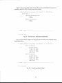
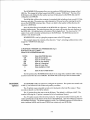
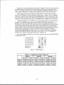
Appendix A provides a complete listing of CMF8580specifications.Figure i-1 shows the
interfacesand major componentsof the CMF8680.
p2
I
I
I
I
I
I
I
I
I
I
RoM-Dos
& Bros
p8
FLoppyDRrvE
\
oPf.!9ry*.9Y102
P7
cGAcRr/LcD lqB {EI|3P
\
\\t-/
scnnr.rr'ca
pl
oi,inn
-rlf,l.B!r,
P6
PARALLELPORT
P9
RS.232 SERIAL
POBT
lMB SOLID
STATE DISK
P5
RS-485SERIAL
PORT
utt,,-1r"
*\.
P10
IDE INTERFACE
NONVOLATILE
P11
CONFIGURATION
RS.232 SERIAL
EEPBOM
PORT
(on bottom)
Figurei-1- CMFB680
cpuModule
i-3
P3
POWER
c&T F8580
PC/CHIPTM
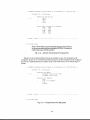
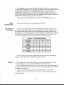
A true single chip PC, the Chips & Technologies'F8680PCICHIPTMfeatures 76-bit, L4
MHz XT compatible performance,low power consumption, the SuperStateR management
system,direct PCMCIA card support, power management,and flexible memory support. Its
on-chip CGA controller provides direct support of CRT or LCD panel displays.
The82C721.super peripheral controller chip adds two serial ports, one parallel port, and
up to two high density ftoppy drives (A: and B:).
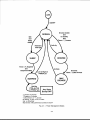
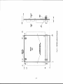
Figure i-2 shows a basicblock diagram for the F8680.Complete specificationsare provided in Appendix A.
F8680
CPU
1MB
sso liiil" LlflH'j$""
zueonou[.,,.,1
i,,,,1
[;.,
lllllll
l::.1
:::i
Figurei-2 -
ABOUT THIS
MANUAL
I
FB6B0BlockDiagram
This manual is written for CMF8680usersdnd systemintegrators. Flere'swhat you'll
find in this manual:
Chapter 7, "Hardware," describesthe different types of memory included on your
CMF8680,interrupts, DMA, and the interfacesyou'll use to attach devicesto your CMF8680.
Chapter 2, "Installation," explainshow to stack your CMF8580with other modules and
prepareyour systemfor power-up.
Chapter 3, "Start Up," explains the setup software configuration and how you can
modify it; systemboot options; and systemBIOS and SuperStaterMR.
Chapter 4, "Power Management" explains the power saving modes of the CMF8680.
Chapter 5, "Using the Solid StateDisk," describeshow to build a ROMDISK.EXEfile for
use the 32-bit byte-wide SSDsocket.
Chapter 6,"CM102 utilityModule: PCMCIA Memory and Keypad Scanning" describes
the PCMCIA interfaceand X-Y matrix keypad scanning.
i-4
Appendix A, "Specifications,"summarizesthe technicalspecificationsof the CMF8680.
Appendix B, "Memory and I/O Maps," presentsthe CMF8680memory andl/O maps.
Appendix C, "Connector Pin Assignments,"provides the pinouts for eachCMF8680I/O
connector.
Appendix D, "Application Notes," contains a current set of CMF8680application notes.
Appendix E, "Warranty," details Real Time Devices'warranty.
REFERENCES
Thesereferencebooks are available for the F8680PCICHIP by Chips and Technologies:
F8680PC/CHIPData Sheet,Publication Number DS133
Reference
Manual, Publication Number UG75
F8680PC/CHIPProgrammer's
F8680PC/CHIPApplicationNofes,Publication Number AN75
IMPORTANT
If you have trouble using your CMF8680cpuModule, or if you need more in-depth
information for your application, call us Monday through Friday between 8 a.m. and 6 p.m.
easterntime at (874)234-8087or fax us 24 hours a day at (81,4)2M-5218for a prompt reply.
i-5
CHAPTER 1
Hardware
1-1
This chapter describesthe different types of memory supported by the CMF8680,interrupt and DMA channels,and interfaceconnectors.This information is useful for configuring
the hardware before installation into a system.
MEMORY
DEVICES
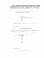
2 MB Dynamic RAM - The CMF8680includes 2 MB of 16-bit wide DRAM installed as
shown in Figure 1-1.Four LM x 4 20-pin ZIP memory devicesprovide 2 MB of memory to be
used as system RAM, shadow RAM for ROM, and 1MB of extended memory which can be
configured as expandedmemory or a RAM disk.
32 KB Static RAM - This on-board SRAM is used for the CGA graphics display (U3,
bottom side of module).
255 KB ROM - This device,shown in Figure 1-L,containsthe XT BIOS,IDE hard drive
R code,and RTD BIOS enhancements.
BIOS,Datalight@ROM-DOS,SuperStaterM
4 K bit Configuration EEPROM - This non-voltatile memory storesthe system configuration with 2 K bits availablefor user and keypad layout (U22,bottom side of module).
Solid StateDisk EPROM (1MB Solid StateDisk) - The CMF8680supportsup to 1MB
of memory installed in this standard 32-pin,byte-wide JEDECsocketshown in Figure 1-1.Up
to 1M x 8, 32-pin memory devicessuch as non-volatile RAM, PROMs,and flash EPROMscan
be installed.
When using the byte-wide socket,you must configure the jumpers on header connectors
A through E for the type of device you have installed. Figure 1-2shows the jumpers and lists
the signal carried and pin number on the byte-wide socket.By installing jumpers on A and D,
and 27C080EPROMsare supported.
27C010,27C020,27C040,
NOTE: To accessa ROM disk, you must enablethe ROM-DOS BIOS extensionin the
RTDMOD setup program, or boot from a floppy or hard disk using the provided Datalight
ROM-DOS.
CAUTION: Make sure that jumpers A through E are properly configured for your
device. Failure to do so can causedamageto the device.
ROM.DOS
& BIOS
1 M BS O L I D
STATE OISK
32 KB STATIC RAM
(U3 on
undersideot module)
2MB DRAM
SSD JUMPERS
A.E
Figure1-1- CMF8680
MemoryDevices
1-3
Jumper
Signal
SSD Pin
A
+5 volts
1
B
ADR19
1
D
E
ADR18
1
ADR18
31
31
MEMW-
jumperson A andD as shownin thisdiagramsupports27C010,
NOTE:Installing
Thesejumpersarelocatedin the lowerleft
& 27C080EPROMs.
27C02O,27C040
cornerof theboard.neartheSSDsocket.
Figure1-2- Byte-WideSocketDeviceJumpers
INTERRUPTS
Eight interrupt channels,IRQ0through IRQ7, are provided by the PC/lO4bus. IRQOand
IRQ1 are reservedby system functions. IRQ2 through IRQT are available to the user for
peripheral devices.The list below shows the interrupt channel assignments:
to theuser)
IRQO:TimerChannel0 (notavailable
(notavailable
Interface
to the user)
lRQl: Keyboard
Theseperipheral devicescan be disabled and their interrupts made available for user
applications:
lRQ2:Video
lRQ3:COM2,COM4
lRQ4:COM1,COM3
lRQ5:IDEHardDisk
lRQ6: FloppyDriveController
lRQT:ParallelPort
DMA
INTERFACE
CONNECTORS
Four DMA channels,DMA0 through DMA3, are provided by the Pc/104bus. DMAO
and DMA2 are reservedfor svstemuse.DMA1 and DMA3 are available to the user for DMA
transfer operations.
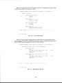
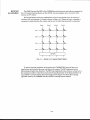
The CMF86B0'sversatility is enhancedby the many on-board interfacesprovided. These
interfacesinclude a 16-bit IDE hard drive interface,high density floppy controller, PCMCIA
interface,CGA CRT/LCD graphics controller, two RS-232serial ports, one RS-485serial port,
an AT enhancedbidirectional parallel port, XT keyboard and speakerports (utility connector), and power connector.Figure 1-3shows theseinterfaces.The following paragraphs
describeeachinterface.Pin assignmentsfor all connectorsare included in Appendix C.
NOTE: The CMF8680is availablewith (CMF8680-2)or without (CMF8680-1)
the PCMCIA connector,P2, and P1 and/or P2 arc available as stackthrough
or soldertail connectors.
ConnectorsP3 through P8, P10,and P11 are normally supplied as right angle
connectors,and P9 is normally supplied as a vertical connector.OEMs can
specify any combination of right angle and vertical connectorsfor P3
through P11.
r-4
P8
FLOPPYDRIVE
P7
CGA CRT/LCD
\
P2
OPTIONALCM102
PCMCIA& KEYPAO
SCANNING(32-pin)
P1
xT BUS (64-pin)
P6
PARALLELPORT
rc
RS-485 SEBIAL
PORT
-P4
/ uTtL|TY
-=\rotf.*
P10
IDE INTEBFACE
P11
85.232 SERIAL
PORT
Figure1-3 - CMF8680cpuModuleInterfaceConnectors
IDE Hard Drive
Interface
The L6-bit IDE hard drive interface,P10,is a standard 40-pin connector.This interface
supports 16-bit data transfersin a single cycle.P10can be connectedto the CM104 1.8inch
hard drive utilityModulerM or to any other 16-bit IDE hard drive.
Floppy Drive
Interface
The high density floppy drive interface,P8, is a 34-pin connectorwhich supports two
high density floppy drives (360K 720K,1".2MB,or 1.44MB)configured as disk drives A: and
B:. Note that eachof the two PCMCIA cards supported by the system are also accessedas
disk drives A: and B:. Therefore,the systemcan support a combined total of two floppy
drives or PCMCIA cards.
PCMCIA
Interface
The P2 PCMCIA interface,included on the CMF8680-2module, is a 32-pin connector
which mates to the CM102 PCMCIA utilityModule. This 32-pin auxiliary bus stacksdirectly
with the CM102 utilityModule, requiring no additional external cabling. SRAM cards,ROM
cards,and EPROM cards which adhereto the PC Memory Card Intemational Association
Release1.0standard can use this interface.Memory cards of up to 32 MB can be read and
written (SRAM only) through this interface.
Keypad
Scanning
The CM102 utilityModule adds X-Y matrix keypad scanningwhich is supported in the
CMF8680BIOS.The keypad layout is user programmable,and the keypad can be used with
or without a standard XT keyboard.
CGA CRT/LCD
Graphics
Controller
The CGA CRT/LCD graphics controller, P7, is a 10-pin connectorwhich interfacesto
most popular CGA and LCD flat panel displays. This interfacesupports 80 x 25 and 40 x 25
text modes, as well as 640 x 200pixel 2-coIor,320x200 pixel 4-color, and 640x 400 double
scangraphics modes.\Alhendriving a CRT or LCD panel, the CGA graphics controller
displays colors or up to 16 shadesof grey.
1-5
RS-232Ports
Two 16450compatible RS-232serial ports, P11 and P9,provide support for user peripherals such as a mouse or modem. P11is from the F8680CPU chip and can be programmed as
COM1, COM2, or disabled.P9 is from theS2CT2Lcontroller chip and can be programmed as
COML, COM2, COM3, COM4, or disabled.Both serial ports operateat up to 115Kbaud.
RS-485Port
The RS-485serial port, P5, supports multidrop systemconfigurations where several
devicesare controlled through a single port. It can be programmed as COM1, COMZ, COM3,
or COM4. \A/henusing P5, you must configure the associatedjumper on header cormector
P14so that the line is terminated or not terminated. The RS-485path must be terminated at
both ends for proper operation. If the CMF8680is at the end of the path, then install the
jumper atPL4 to terminate the line. If the CMF8680is located somewherein the middle of the
R$485 path, remove the jumper at P14so that the line is not terminated. Asserting the RTS
signal on the serial port enablesthe RS-485driver. The RS-485receiver is always enabled.The
RS-485usesa 16450compatible UART.
Parallel
Port
Utilitv Port
This port, P6, can be programmed as aPC/ AT enhancedbidirectional parallel port or as
a standard printer port and can be program.medat address3BCH, 378H, or 278H, or disabled. The parallel port cable should be lessthan 10 feet long to ensure reliable data transfer.
The 10-pin utility port,P4, provides XT keyboard signals,piezoelectricspeakersignals,
system reset,suspend,/resumeswitch signal, sleepmode monitor, and battery backup
connections.The pin assignmentsare given below. The speakersignal can drive an external
piezoelectricspeaker.\Atrhenthe RESETline is taken low at pin 3, a systemreset occurs.Pin 4,
PWRUP, is used to place the systemin and out of the suspendmode for power conservation.
\A/henconnectedto a slide switch, a high keepsthe system in the run mode and a low places
it in the suspendmode. \A/henconnectedto a pushbutton switch, the mode togglesbetween
run and suspend eachtime the switch is depressed.The switch type is user configurable
using RTDMOD.EXE (seeChapter 3, Power ManagementSetup discussion,for more details).
Note that the PWRUP signal must be properly debounced.An XT keyboard with a standard
S-pin DIN connectoris connectedto pins 5 through 8. A normally open reset switch can be
connectedbetween pins 3 and GND. A battery to back up the real-time clock can be connected between pins 9 and GND. Pin 10 is low when the cpuModule is in the suspend mode.
PIN
PIN
SIGNAL
SIGNAL
1
+SPKR
6
_KBCLK
2
GND
7
GND
3
RESETSW-
I
PWRUP
o
KBDPWR
+3.6VDCbatterv
-SLEEPY
4
-KBDATA
10
7-6
Power
Connector
Power is provided to the CMF8680through the 8-pin power connector,P3. This connector is not used if power is provided through the XT bus. The table below shows the pin
assignmentsof this connector.The CMF8680requires only +5V and GND. The remaining
voltagesare supplied to the PCl104 bus.
PCl104
ExpansionBus
SIGNAL
-5V
1
GND
PIN
5
2
3
+5V
6
-12 V
N/C
7
GND
4
+12Y
I
+5V
PIN
SIGNAL
The 54-pin PC/104 XT compatible ISA expansionbus, P1, allows you to directly stack
PC/ L04compatible modules.
1n
1-8
CHAPTER 2
Installation
2-1,
This chapter describes the installation procedures for integrating the CMF8680 into a
PC/104 system.
STACKING
MODULES
The CMF8680can be stackedwith other PC/1,04form factor modules to form a cubical
system,as shown Figure 2-1.\,Vhenstacking the CMF8680,first make all of your peripheral
connections.Be sure to connectpin L of the cable to pin L of the corurector.The connectorsare
labeled on the board. If you cannot read the label, pin L can be identified by its square solder
pad, visible on the top and bottom sidesof the module.
After all peripheral connectionsare made, insert the pins of the PC/104 expansionbus of
one module into the socketson the secondmodule, making sure the pins are properly
aligned before seatingthem into the sockets.The order of the modules in the stack is not
important as long as all modules in the middle have a stackthrough PC/104 bus connector.
After the modules are stacked,insert the spacersprovided with eachmodule to securethe
stack.Figure 2-2 shows a typical stack.The stack is now ready to install in your system.
NOTE: Sincemost dataModules do not have the extra 32-pn auxiliary bus connector,we
recommend that, if you have the -2 version of the CMF8680with the optional P@PCMCIA
connector,you place dataModules on top of the CMF8680and utilityModules under the
CMF8680,as shown in Figure 2-2.
32-PtNCM102 PCMCIABUS
\
cMF8680
cpuModule
64.PINPCl104BUS
\
'.{,,.}
{*diip
tl,"il
'-w
PCMCIA CARD-
cM102
utilityModule
Figure2-1- PC/104Stack
2-3
*-/
(DM5406)
dataModule
(CMF8680)
cpuModule
(CM102)
utilityModule
H
U 0.6'SPACEF
0.6'SPACER
(2rows
withonlya P1connector
NOTE:Wheninstalling
a dataModule
of pins),makesurethatthe2 rowsof pinsengagewiththe2 rowsof
pinsclosesttotheedgeof
inthediagram.
module,
asshown
themating
Figure2-2 - TypicalStack Assembly
OTHER OPTIONS
br addition to stacking,modules can be connectedto backplanes,other boards with a
PC/L}4bus connector,or in a number of custom configurations, depending on your application. If you need help with hardware installation, pleaseconsult the factory.
2-4
CHAPTER 3
Start Up
3-2
This chapter tells you how to use the configuration setup program, RTDMOD.EXE, and
how to start up your CMF8580.Systemboot options, the BIOS and SupterStateR" and the
watchdog timer are also discussedin the chapter.The settingsshown in the manual are the
default settings.
RTDMOD
SETUP
pROGRAM
The system configuration program/ RTDMOD.EXE,is used to set up the various parameters of the CMF8680before you boot the system.The setup program is on a utility disk
shipped with your CMF8680.To run the setup program/ you will need a CRT, keyboard, and
floppy drive. The setup program can be placed in a ROM disk, or on the hard drive, if
desired.
The first screenin the RTDMOD setup program is shown in Figure 3-1.When the program starts, it loads the settingsfrom the configuration EEPROMto ensurethat you are
is proworking with the actual systemconfiguration. A default setting, RTDDFLTO.SET,
vided. If you should get into trouble when configuring your system,such as turning off the
CRT display, you can hard resetthe systemand simultaneously hold down both <Shift> keys
and the system will boot using the default settingsin the BIOS.The RTD utility ROM disk
must be installed in the user EPROM socket.The default settings are:
Drive A: 5-114inch 1.2Mfloppy
Drive B: PCMCIA
IDE disabled
ROM-DOS enabled
CGA graphics on a CRT
The main page lets you load the current settings,savethe new settings,and then exit the
program or abort the new setup. The current settingscan be loaded from the EEPROM,the
default file, or from a user file. Settingscan be saved to any one of thesethree locations.The
abort/exit menu lets you revert to the last saved configuration, exit with a hard reset (a hard
reset is necessaryto implement most con{iguration changes),or exit to DOS without making
any changes.The HELP menu is also shown in Figure 3-1 at the bottom of the screen.In
addition to the keystrokesdescribedin HELP, ESCwill send you back to the Main Page.
-CMF8680
cpuModule Setup Progrdm vl .06 Copyrighl
Main Page -
Save, Load, Aborc or
Load Settings:
FTom EEPROM
Configurat.ion
(c)
1993 RTD USA-
Exit:
Data fron
(RTDDFLTO.SET)
Default
i,il"
;:::)fl5:=";"3:'?,:;'l
Save Settings:
TO EEPROM
Confj-guration Data as Default
DaLa to a Pile
Configuration
User/Keypad Data to a FiIe
Abort
/
-";tt;
ro Lasr Load
Exit with Hard Reset
EX1T TO DOS
Help,/
SeIecL --=> Exit
f^n+inrrrriinr
IIc6r/KF\/h:.1
d:t:
tr1
Lra ln
f ^r
Mnra
rnr
to DOS (or <ESc>), if
^rts:
ic
i. c-
al
n
vn
r rl rr rf
(RTDDFLTO.SET)
l
na^ac
rha
d^f
ov.ani
a
cnforod
you wish to Quit
iha
Tlaar/KF\rn^ri
an
rhc
Fig.3-1- SetupProgram
MainPage
J-J
d- :- r-: *
llcar/KF\/n^d
r,-
r age.
p
uaLd
lJagc.
The F1 more help screenfor Figure 3-1.looks like this:
-Help
/
In
qne.a/F'nfpr-qp-pCLS
ALT-C
ALT-X
TAB or Down Arrow or Left Arrow Move forward
PageDn Next Screen
ALT-D GoLo DrsDlav Screen
SHIFT TAB or Up Ariow or Right Arrow Move backwards
Toggle Colors
Goto Marn Screen
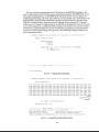
The next screen,shown in Figure 3-2,lets you set the CPU clock frequency.
-CMF8680
cpuModule Setrp
q\rciam
aI^^L
>
-H61
^
P-rogram VL . 06 Copyr j ght
(c ) 1993 RTD USA-
eh66/l
L4.318 MHz
1.I59 Mhz
4.173 Mhz
3 .580 Mhz
/
a1'c
ts 6m
r'l
nnlz
tr1
f ^r
M^rp
qncart
controlfers
wiff
not work reliably,
is set below 4.7'/3 Mhz.
if
the
LIa I n
Fig.3-2- CPUSpeedScreen
The PC104Bus and 721AccessSpeedscreen/shown in Figure 3-3,setsthe number oI
CPU clocksper bus accessand enables/disablesthe DRAM refresh cycle.
-aMtrRKQO
cnrrMnrirr'la
qairrn
e L L q P
Dr^dr^m
\/1
r ! v v r q r "
v ,
O6
r v v
annrrrinhf
v v y J
/r\
1aQ?
PC104 Bus and'12L Access Speed:
CPU Clocks per
One
Two
'Inree
Four
.\/.16a
^n
PC104 Bus
Enabled - Slows System
Disabled
Rcfrech
>
-HFtn
Pofroch
!1
tor
/
nT
a\/.1
Fc
More
are
Bus and 721 Clock
onlv
required
for
certain
PCl04 boards.
Heap
Fig.3-3- CPU Clocks/Refresh
3-4
RTD USA-
Figure 3-4 shows the enable/disable for the IDE hard drive and ROM-DOS.Systemboot
options are defined in Table 3-2 near the end of this chapter.
-CMF86B0
cpuModule SeLup Program Vl .06 Copyright
(c)
1993 RTD USA-
Device Control:
IUE
H A T O 1 J I S K T JL U S E X I E N S l O N :
Enabfe
>
Disable
ROM*DOS BIOS Extension:
>
Enable
Disable
-uFln
F1 for
/
rrf^
More Help
Fig. 3-4 -
IDE Hard Drive, ROM-DOS Enable/Disable
The next screen/ shown in Figure 3-5, configures drive A: and drive B:. The system can be
booted from drive A:.
-aMFa
A Q n
nnr
rMndr
copyrighr
r'l a
Devlce
(c)
A: Selection:
No Drlve Present
360 KB 5 L/4 Drive
1.2 MB 5 L/4 Drive
720 KB 3 1/2 Drwe
1 . 4 4 M B3 L / 2 D r i v e
PCMCIA Card
Devrce
B: Selection:
No Drrve Present
360 KB 5 1/4 Drlve
1.2 MB 5 l/4 Drwe
120 KB 3 1/2 Drwe
1 . 4 4 M B3 L / 2 D r w e
PCMCIA CaTd
-Hefp
F1 for
/
rnf
More Help
Fig.3-5- DriveA: andDriveB: SetuP
3-5
1993 RTD USA-
The IDE hard drive type is specifiedon the screenshown in Figure 3-6.The standard
table for fixed disk drive types L through 47 is listed in Table 3-1.
It is recommendedthat you selectuser programmable drive 48 or 49 so that you can be
sure the drive is configured correctly. If you choosethe custom values (48 or 49),then you
must fill in the next screen,shown in Figure 3-7.Note that you must enter all of the placesin
eachnumber: for example,00650cannot be entered as 650 on the first line.
-CMF8680
cpuModule
luE
IJrlve
Setup
LU.LL:
h
F1 for
More Help
1993
(0-14
or
1"6-47)
(0-14
or
16-47\
/
Fig.3-6 -
-CMF8680
IDE Hard DriveSetup
cpuModule Setup Program V] .06 Copyright
.LIJE LUSTOM
UTlVC
(c)
1993 RTD USA-
SELL]NqS:
Custom Value #48
00547 Cylinders (00000-65535)
008 Heads (000-255)
(000-255)
038 Sectors per Cylinder
00547 Landing Cylinder
Custom Vafue #49
(00000-65535)
00980 Cylinders
010 Heads (000-255)
(000-255)
017 Sectors per Cylinder
00980 Landinq Cylinder
F1 for
RTD USA-
UTIVE:
Tabl-e >49
Standard
#48
Custom Drive
#49
Custom Drive
UCIAUIC IDE D: DTIVC:
>
standard
Table >00
Custom Prive
#48
#49
Custom Drive
-u61
(c)
Copyriqht
SeIectIon:
UEIAUIT
>
V1 .06
Program
More Help
Fig.3-7- IDECustomDriveSettings
3-6
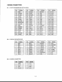
Table3-1 - StandardIDE Hard DriveTable
Fixed disk type 1
Fixeddisk type 2
Fixeddisk type 3
Fixeddisk type 4
Fixeddisk type 5
Fixeddisk type 6
Fixeddisk type 7
Fixeddisk type 8
Fixeddisk type 9
Fixeddisk type 10
Fixeddisk type 11
Fixeddisk type 12
Fixeddisk type 13
Fixeddisk type 14
Fixeddisk type 15
Fixeddisk type 16
Fixeddisk type 17
Fixeddisk type 18
Fixeddisk type 19
Fixeddisk type 20
Fixeddisk type 21
Fixed disk type 22
Fixeddisk type 23
Fixeddisk Wpe24
Fixeddisk type 25
Fixeddisk type 26
Fixeddisk type 27
Fixed disk type 28
Fixed disk type 29
Fixeddisk type 30
Fixeddisk type 31
Fixed disk type 32
Fixed disk type 33
Fixed disk type 34
Fixeddisk type 35
Fixeddisk type 36
Fixeddisk type 37
Fixeddisk type 38
Fixeddisk type 39
Fixeddisk type 40
Fixeddisk type 41
Fixed disk type 42
Fixed disk type 43
Fixed disk type 44
Fixed disk type 45
Fix€d disk type 46
Fixed disk type 47
Cyl
Heads
WPC
306
615
4
4
otc
b
128
300
300
512
512
NONE
256
NONE
NONE
NONE
NONE
NONE
128
NONE
0
0
300
NONE
512
300
300
300
NONE
305
300
NONE
NONE
NONE
NONE
NONE
NONE
128
NONE
NONE
0
NONE
128
NONE
NONE
NONE
NONE
NONE
NONE
NONE
NONE
NONE
NONE
940
940
615
462
733
900
820
855
855
306
733
0
612
977
977
1024
733
733
733
989
612
612
614
820
977
1023
1024
1024
809
830
aen
776
1024
615
615
925
1024
80
160
672
522
980
980
862
8
6
4
I
15
3
tt
0
4
7
7
7
12
4
2
4
5
o
8
o
10
b
tt
tt
8
9
9
2
2
tt
4
5
10
4
3-7
Control Land
Sec
305
615
615
940
940
615
511
733
901
820
855
855
319
733
00
663
977
977
1023
732
732
733
989
663
612
614
820
977
1023
1024
1024
809
830
830
775
1024
615
615
925
1023
80
160
671
522
980
980
862
17
17
17
17
17
17
17
17
17
17
17
17
17
17
17
17
17
17
17
17
17
35
17
17
17
17
17
17
17
17
17
17
17
33
17
17
17
17
17
32
32
39
40
17
17
38
The next three screens,Figures3-8 through 3-10,configure the serial ports and the I/O
addressfor COM3 and COM4. The three serial ports are 1"6450
compatible serial ports that
operateat up to 115.2Kbaud.
----CMF8680 cpuModule Setup Program V1.06 Copyright
(c)
1993 RTD USA-
PC/Chip RS232 Port:
COM Port
& Address:
>
COM 1
3F8H
COM 2
2FBH
Disabled
None
-Hal
tr1
n
f^r
/
M^r6
HFln
Fig.3-B- F8680RS-232SerialPortSetup(P11)
cnr:Modr:le Sef rrn prooram
-CMF8680
12L
On-Board
I/O
\/1 .06
Cnnw-inhr
le )
1qq1
Settlngs:
RS232 PorL
COM SeLLjng:
COM I
COM2
>
COM 3
COM 4
Disable
Fl
^^^\,
>
aartrnl
I ar.
Enabfe
Disable
-Help
F1 for
/
More Help
Fig. 3-9 -
82C721RS-232Serial Port Setup (P9)
3-8
RTD USA-
-CMF8680
cpuModule Setup Program V1 .06 Copyright
On-Board 72L I/O
{c)
1993 RTD USA-
Settlnss:
RS485 Port COMSetting:
coM lCOM 2
>
COM3
COM 4
Select
>
F1 for
COM3 and COM4 I/O Address;
COM3
COM4
33BH
238H
3E8H
2E8H
2EBH
2EOH
220H
228H
More Help
because
someofthepins
NOTE:TheRS-485portcannotbedisabled
Thisdoesnot
EEPROM.
onthisportaresharedwiththeconfiguration
interfere
withproperRS-485operation.
Fig.3-10-82C721RS-485 SerialPortSetup(P5)
Figure 3-11shows the parallel port mode and addressscreen.The extended mode
configures the port as an AT enhancedbidirectional port, and the standard mode configures
the port as a standard printer port. Either mode can be used when you are interfacing to a
printer.
-CMF86B0
cpuModule Setup Program V1 .06 Copyright
(c)
1993 RTD USA-
On*Board 72L T/O Settinqs:
Parallel
>
Parallel
>
Port Mode::
Port
Extended ParallelMode
Standard Printer
Port
3BCH
3 /UH
Mode
Address:
PU
SLANOATO
2 78 H
Disable
-Haln
F1 for
/
More Help
Fig.3-11- Parallel
PrinterPortSetup(P6)
3-9
Figure 3-12configures the intemal graphics controller. Rememberthat if you disable the
controller, you will not have CGA graphics and you must make sure that you have another
display device (e.9.,VGA card and monitor). When using a standard VGA board with the
CMF8680,it is not necessaryto disablethe CGA graphics;however, most VGA boards will
try to emulate the CGA modes, and this could causeproblems.
--r-MFC6R0
c6F,.i
enrrMod.rla
!LLuy
PC/C^i n Cranhic
r:ranh
i .
>
D
r^^rir
!rvY rqr"
Corrrol
a^nr
Y^l
\v/ r1
leI ar
n4
rvv
fl v^ynj \ / r i ^ h i
F1 for
RTD
USA-
.
Enabled
Disabled
9 Dot Cl-ock Character
Enabled
>
oisabled
/
1qq1
Co-fiouration:
Dot Clock Select:
>
T4.318 MHz OSC
optional
oSC - Make sure
-He1p
//.\
instaffed
Mode - CRT only:
Info
More Help
Fig.3-12- GraphicsControllerSetup
Figures 3-L3through 3-15show the screensfor the CGA CRT/LCD graphics setup.
Figure 3-13selectsone of the four positions for the Dot Clock.
-cMF8680
cpuModule
PClChip Graphic
uot
>
SeLup Proqram Vl .06 Copyright
Contro]1er
u]ocK Sl.qnar:
Enabled
Disabled
Presets
SYNC to
(c)
l-993 RTD USA-
- Dot Signals:
Ground
Dot Clock Phase:
>
Late
Early
>
-q6l
F1 for
h
Normal
Inverted
/
More Hel-p
DotSignals
Fig.3-13- Graphics
Controller,
3-10
Figure 3-14allows inverting of various video signals.
------{MFB6B0 cpuModule SeLup Program Vl.06
PC/Chip Graphic
Pixel
>
Copyright
Presets
Controller
- Signal
(c)
1993 RTD USA-
ComplemenLs:
Signals / Inverse Video:
Normal - No Complement
rrvarca
-
.^r^lement
Horlzontal Sync:
>
No ComplemenL
Complement
VerLical Sync:
>
No Complement
Compfement
-H-l^
Fl- for
/
More Hefp
Fig.3-14- Graphics
Controller,
SignalComplements
Figure 3-15 selects the font which is displayed and the blink rate options.
-aMtrQAQn
nnrrMnd,rl6
PClChip Graphic
qafilh
JcLUV
D rr ^vdVr r^ o
m
E
Concroller
Standard Font:
>
Fi rsL FonL
Second Font
Translate
Intensity
Enabled
>
Disabfed
\/1
- AIt
nA
aL ^vnp\ tr -r ir^yhrr r -
r-l
\L/
Font and Blink
-YYJ
RaLes:
(BOLD Font)
Bit
as Font
Selection:
Character Bl ink Rate:
Vafue j-s >00 [0-16 Dec]
Cursor
- H d l n
F1 for
/
Blink Rate:
Value is >02 [0-16 Dec]
l n f
More Help
AlternateFontand BlinkRates
Fig.3-15- GraphicsController,
3-11
Figure 3-16controls the CRT or LCD selectionand the LCD parametersfor grey scaling,
first line marker delay,and double scanmode.
-CMF8680
cnil\4odulp
Pc/Chip
qFf rln
!vuuw
p
r^nr^m
! !vvrqr"
\v/ r1.
O
v vA
a
L vnv n
f !r ' - i n h *
l.)
1qo?
USA -
RTD
LCD Control:
craphic
>
Controller
CGA CRT
CGA LCD
Mode:
Grey Scaling:
>
4x2 box ( l- 6 Color )
4x4box(SColor)
First
>
Line Marker Delay:
No Defay
Add Delay
DOUD1E
>
-Help
F1 for
SCAN
LCLJ:
Normal-scan
Double-scan
mode (200-line)
node (400-line)
/
More Help
Fig.3-16- LCD ControlSetup
Figures 3-17 and 3-18show the BaseMemory addressing.It is recommended that the
factory settings (PC/104 BUS) or RAM be used unless you have complete information about
the PC/CHIP memory managementin order to avoid contention.
-CMF8680
cpuModule Setup Progfram Vl .06 Copyright
Base Memory Control
- A0000 & 80000
(c)
1993 RTD USA-
(Non-t"tapped):
A0000-AFFFF Range:
RAM
>A000 [0000 /
User RoM at offset
Custom Value >00 [Hex Byte]
>
PCl04 Bus
2AAA
B 0 0 0 0 - B F F F F R a n g e : ( S e t t o P C 1 0 4 B u s f o r CGA)
RAM
>8000 11000 / 3000
User RoM at offset
Custom Value >00 [Hex Byte]
>
PC104 Bus
p/
F1
for
More
HelP
Fig.3-17- BaseMemory,
Screen1
3-12
/ E0001
/
F0001
-cMF8
6I 0 cpuModule
Setup
BaSe Memory Control
Program V1.06
Copyrigrht
(c)
1993 RTD USA-
- C0000 & D0000 (Non-Mapped) :
C0000-CFFFF Range:
RAM
U s e r R O Ma t O f f s e t > C 0 0 0 [ 0 0 0 0 /
CusLomValue >00 [Hex Byte]
>
PCI-04 Bus
2000 ...
/ E0001
D0000-DFFFF Range: (Norma11y used for EMMSystem)
RAM
U s e r R O Ma t O f f s e t > D 0 0 0 [ ] - 0 0 0 / 3 0 0 0 . . . / F 0 0 0 1
Custom Vafue >00 [Hex Byte]
>
PC104 Bus
tr1
f^r
M^ro
Haln
Fig.3-18-
BaseMemory,Screen2
Power managementoptions are shown in Figure 3-19.The PWRUP switch type and
polarity are set here according to the switch connectedto utility connectorP4, pin 4. Refer to
Chapter 4 for more information about power management.\Alhilethere are many possible
combinations of switch type and mode of operation of the PWRUP signal, the following
paragraphs describesomeways you can implement this feature.We will look at slide and
momentary switch operation to describethe basic function of the PWRUP signal.
NOTE: It is very important that any switch connectedto the PWRUP signal
be properly debounced.
Slide Switch Operation: \A/henthe PWRUP signal is high, the CMF8680is running, and
when PWRUP is low, it is in the suspendmode. To implement this configuration, use
RTDMOD.EXE to set the PowerUp Switch Type to Slide and the PowerUp Switch Polarity to
Switchon PWRUPgoingHigh. The switch you connectto the PWRUP signal can be a slide
switch that is open in one position and grounded in the other position (PWRUPis intemally
pulled up on the CMF8680).When the switch is open, the CMF8680will run, and when it is
grounded, the CMF8680will be in the suspendmode. A normally open momentary pushbutton switch can also be used in this configuration. When the button is released,the
CMF8680is running, and when it is pressed,the CMF8680entersthe suspend mode.
Momentary Switch Operation: This mode requires that you use a normally closed pushbutton switch connectedto the PWRUP signal. PWRUP should be low for normal operation.
\A/henPWRUP is brought high and then back to low, the CMF8680enterssuspend mode.
When PWRUP goeshigh and then low a secondtime, the CMF8680resumesrunning. To
implement this configuration, use RTDMOD.EXEto set the PowerUp Switch Type to Momentary and the PowerUp Switch Polarity to Switchon PWRUPgoingLow.
If you do not use the PWRUP signal, set the PowerUp Switch Polarity to Disabled.
3-13
-cMFR6R0
qats, n
cnilModulp
l L L s v
p-^nrFI
\/1
O$ Qepyaight
(c)
1993
RTD USA-
and Swicch options:
Power Conservation
Power Saving:
>
No Power Savings
Sleep only
Sleep + Drowse Modes
Sleep + Drowse - Suspend Modes
Idfe
Time Before Suspend
060 rines 2 Minures
D^r,r6rTln
>
ts-h
Trrn6.
Momentary
5rr(le
Powerup Switch PolaritY:
S w i t c h o n P W R U Pg o i n g h i g h
S w i L c h o n P W R U Pg o i n q l o w
oisabled
>
F1 for
CL'i
(001,255)
More Help
Fig.3-19-
PowerManagementSetuP
Figures 3-20through 3-24letyou selectwhether the CGA video information is stored in
the BIOS or in the EEPROM.If you selectthe EEPROM,you must set eachvalue on the
screensshown in Figures 3-20through 3-24.The CRT controller is 6845compatible.
CMTRAQO
nnrrMadillp
qpfrrn
Jsuuv
p
rndrtm
! !vY rurrr
\/1
06
(-^nvriohr
(e)
19ai
p1p
USA-
PC/Chip CGA Video Modes:
Location of Video Information:
>
BIOS ROM / EPROM
all
E E P R O M( T h i s r e q u i r e s
values
to
Mode Register Values IHex BYtes]
2C Mode 0 - 40x25 Mono Text
28 Mode L - 40x25 Color Text
2D Mode 2 - 80x25 Mono Text
29 Mode 3 - 80x25 Color Text
2A Mode 4 - 320x2AA 4 Color GraPhics
2E Mode 5 - 120x200 4 Mono CraPhics
1E Mode 6 - 620x200 2 Color GraPhics
29 Mode 7 - 80x25 Special Mono Text
-Help
F1 for
/
More Help
Fig.3-20- CGA VideoModes
3-74
be setl)
-CMF86B0
PClChip CGA Video Modes Register
40x25 Text Modes
0 38 Register
28 Register
1 *
2A Register
2 3 0A Register
4 _Lf Regrscer
5 06 Regrister
6 19 Register
1 1C Register
9 07 Register
06 Register L0 07 Register 11 0000 Register 12
0000 Register 14
-Hal
n
F1 for
More Help
( c ) 1 9 9 3 R T D U S A-
Copyri ght
cpuModule SeLup Program VI.06
Values
EEPROM:
for
ToLaf
Horizontal
Hnri
znnh:
I
ni cnl
rrraA
Hori
zonfa
I
Hnri
znnf
Svnc
q\/..
Poe i SL ion
r^l:rrl n
:l
verc1ca1
Iocaa
I/6rts i -a
l
ni cnl
^\,6d
\/FrrraF
I
swna
poqrqtfon
ahir.^t6r
a- -a' l . I
H
, , o- i, a- h
. ,, L
Cursor Start
cursor
Encl
& 13 - Start Address
& 15 - End Address
/
Valuesfor EEPROM,
40x25Mode
Fig.3-21- CGAVideoModesRegister
-CMFR6R0
cnrrModrrla
PClChip
qar'rn
CGA Video
Dr^nr^r
\/1
Modes ReqisLer
B0x25 Text Modes:
71 Reqister
0
1
50 Register
2
54 Register
0A Register
3
4
i,C Register
1E R e g is L e r
5
19 Register
6
1
1A Register
07 Register
9
06 Register 10
07 Register 11
0 0 0 0 R e g is c e r
0000 Regiscer
F1 for
n6
Convrioi-f
{e }
for
Values
RTD
USA
-
EEPRoM:
Horizontal
Total
Hnri
ni
znrf:l
lqqj
cnl
arrod
Horizontal
Sync Posistion
Horizontal
Sync Width
Total
Vertical
\/erfieal
I/arts i -r
Tol al
1
Vertical
A.lirrst
ni cnl
r',ad
Sync PosisLion
f-hararf
pr
Cursor
cursor
& 13 & 15 -
Start
-bino
Start
Address
End Address
Ccl
I
HF;dl.t
More Help
Valuesfor EEPROM,
80x25Mode
Fig.3-22- CGAVideoModesRegister
3-15
---CMF86B0
cpuModule
Setup
Program Vl-.06
PClChip CGA Video Modes Reg.ister Values
Graphic
-Haln
I r
/
.ror
More
Modes:
38 Register
0 28 Register
1 2A Register
2 0A Reqister
3 7F Register
4 06 Register
5 64 Register
6 70 Register
1 00 Register
9 06 Register 10 07 Register 11 0000 Reqister 12
0000 Register 14
(c)
Copyright
for
1993 RTD USA-
EEPROM:
Horizontal
Total
Hnri
znnts:l
ni
uori
zo--al
qwn.
Poq i sCion
q\/nr
Wi.lfh
Horizonf
al
c6l
^\/arl
Vertical
\/errieal
Total
ToraI Arirrrsl
\/arf
ni cnl
rrrori
Svne
Poqisfion
i -.1
\/er-iral
ahararfer
Cursor
Cursor
& 1-3 & 15 -
Cel1
Heinht
Start
End
Start
Address
End Address
Trfa
He_LD
Fig.3-23- CGAVideoModesRegister
Valuesfor EEPROM,
GraphicMode
----CMF8680
cpuModule
PClchip
Setup
CGA Video
Program Vl.06
Modes Register
80x25 Special Mono Text
61 Reqister
0 l- 50 Register
52 Reqister
2 0F Register
3 l-9 Register
4 06 Register
5 19 Register
6
19 Register
7 0D Register
9 0B Reqister 10 0C Reqiscer 11 0000 Reqister 12
0000 Reqister 14
-Holn
F1 for
Copyright
Values
for
(c)
1-993 RTD USA-
EEPROM:
Mode:
Horizontal
Total
Horizontal
Displayed
Horizontal
Sync Posistion
HorizonLal Sync Width
Vertical
Total
Vertical
Total Adjust
Vertical
Displayed
Verticaf
Sync Posistion
Charact.er Cell Height
Cursor Start
Cursor End
& 13 - Start Address
& 15 - End Address
/
More Help
Fig.3-24- CGAVideoModesRegister
Valuesfor EEPROM,
80x25SpecialMono
(640x400DoubleScanMode)
3-1.6
The screencontrol is set up as shown in Figure 3-25.The F1,/FZsetup messageallows the
user to changesystemparametersusing the setup provided in the Chips & Technologies
BIOS.
NOTE: Any changesmade in this setup program will take effect as soon as the program
is exited; however, the settingsmade here will not be saved.Also, the data values displayed
for the hard disk types are incorrect.The values used are shown in Table 3-1.
------{MF8680
Setup
cpuModule
Program Vl.06
Copyriqht
(c)
1993 RTD USA-
User Boot Screen Control:
F1lF2 Setup Message:
Display
>
Skip
Clear
>
-r{al
n
F1 for
More Help
screen on boot:
Clear
Skip
/
Fig.3-25- UserBootScreenControl
Keypad scanningis enabled and the size of the matrix is set up in the screenshown in
Figure 3-26.Youcanprogram up to 256keys,as describedin Chapter6. Here, you set up the
number of rows by the number of columns of your keypad. Then go to the user/keypad data
screen(seeFigure 3-28and text) to program the values for the keys.
-CMFRfrqo
enrrModrr'la
Keypad Scanning
qaf rrn
p-^drar
\/1
n6
Convrioht
(c)
199i
RTD
USA
Control:
Keypad scanning:
Enabled
>
Disabled
Keypad size (Set to 0 to free
00 Rows (0-16)
0 Columns ( 0-B )
elp
F1 for
User space in
/
More Help
Setup
Fig.3-26- KeypadScanning
3-77
EEPROM):
Each value of the serial EEPROM is shown in Figure 3-27. Note that the last word contains the signature byte "52" in the low byte and the checksum in the high byte.
-
CMFB680cpuModule Setup Program v1.06
anrFinrrrrti^h
O3LF 7F25
282C 292D
2838 0A2A
5071- 0A5A
2838 0A2A
5061 0F52
0223 0008
FFFF FFFF
(c)
Copyright
1993 RTD USA-
nrts..
FBOO BEBC
2E2A 29LE
061F 1C19
t-ElC 1A19
061F 7064
0619 1919
FFFF FF26
FFFF FFFF
00DE 0000
FFFF FFFF
07FF 0706
07FF 0706
01FF 0706
ODFF0C0B
0223 FFFF
FFFF FFFF
0000
F'FFF
0000
0000
0000
0000
03D4
FFFF
FFFF
FFFF
0000
0000
0000
0000
080A
FFFF
0 3 0 3c E 0 E8 0 8 3 3 8 2 0 3CCO
FFFF
FFFF
FFFF
FFFF
FFFF
FFFF
FFFF
FFFF
FFFF
FFFF
FFFF
COOO FFFF
FFFF FFFF
FFFF FFFF
FFFF
FFFF
FFFF
FFFF
FFFF
FFFF
FFFF
FFFF
FFFF
FFFF
FFFF
FFFF
FFFF
FFFF
FFFF
FFFF
FFFF
FFFF
FFFF
FFFF
FFFF
FFFF
FFFF
FFFF
FFFF
FFFF
I I I I
I T ! I
U J U 4
I I I I
uuJr
ffff
ffff
ftrr
FFFF
FFFF
FFFF
FFFF
rrrf
FFtsts
ffff
uulz
CHECKSUM
SIGNATURE
__>No
changes allowed
,'Lry
mL^
IIle
,.^1..^^
vatues
^-^^^n^i
Ljreceueu
Configuration
tr]
f^r
M^ra
data
l
oy
is
/
a
on this
tnr
neriod
aIl
screen.
are
differenf
r
rha
than
the
Ilcar/Kavn^d
EEPROM values.
d:r
^
n^na
Haln
Fig.3-27-
EEPROMValuesScreen
Figure 3-28shows the screenwhere you program the values for your keypad matrix
when you are using the keypad scanningfeature of the CM102 utilityModule with the
CMF8680.Depending on the number of rows by columns you configured on the screen
shown in Figure 3-26, all or part of this table will be used to enter the scancodes.The portion
of the table where the scancodesare to be entered is highlighted. For example,supposeyou
select a matrix size smaller than 16 rows by 8 columns, such as 4 rows by 2 columns. The
table in Figure 3-28will have the last eight words highlighted to enter your scancodes.\A/hen
your matrix is smaller than the full table, the data words used to enter scancodesare always
highlighted from somepoint within the table to the end. This allows unused memory to be
free for other functions.
When you enter data, the first word (going from top to bottom and left to right) corresponds to row 1, column 1 on the keypad; the secondword correspondsto row 1, column 2;
and so on. Eachword in the table programs two keys: the low byte programs the scancode
for the keystroke when the Fn (or Ctrl + Alt) key is NOT depressed;the high byte programs
the scancode for the keystroke when the Fn key IS depressed.Note that in order to activate
the Fn key feature, at some location in the table, you must define both the low and high bytes
of the SAME WORD with the Fn key scancode.The scancodesare defined in Chapter 6.
Refer to this chapter for complete information on programming scancodes.
3-18
-cMF8580
c^F,'^
cn|Modul-
User
FFFF
FFFF
FFFF
FFFF
FFFF
FFFF
FFFF
FFFF
FFFF
FFFF
trfr
FFFF
FFFF
FFFF
FFFF
FFFF
FFFF
FFFF
FFFF
!ffr
FFFF
rf!r
FFFF
FFFF
FFFF
rrrr
FFFF
rrr!
FFFF
FFFF
FFFF
FFFF
r/1
n4
ConvTiohf
(c)
'lggl
RTD
USA
-
/ Keypad Data:
FFFF
FFFF
FFFF
ffrr
Dr^^,-i
FFFF
FFFF
FFFF
FFFF
FFFF
FFFF
FFFF
FFFF
FFFF
FFFF
FFFF
FFFF
FFFF
FFFF
FFFF
FFFF
FFFF
FFFF
FFFF
FFFF
FFFF
FFFF
FFFF
FFFF
FFFF
FFFF
FFFF
FFFF
FFFF
FFFF
FFFF
FFFF
FFFF
FFFF
FFFF
FFFF
FFFF
FFFF
FFFF
FFFF
FFFF
FFFF
FFFF
FFFF
FFFF
FFFF
FFFF
FFFF
FFFF
FFFF
FFFF
FFFF
FFFF
FFFF
FFFF
FFFF
FFFF
FFFF
FFFF
FFFF
FFFF
FFFF
FFFF
FFFF
FFFF
FFFF
FFFF
FFFF
FFFF
FFFF
FFFF
FFFF
FFFF
FFFF
FFFF
FFFF
FFFF
FFFF
FFFF
FFFF
FFFF
FFFF
FFFF
FFFF
HIGH BYTE .
FFFF
FFFF
FFFF
FFFF
FFFF
FFFF
FFFF
FFFF
.7-
/l
LOW BYTE
Hit
trdiLing
Pageup
Location
/
>
PageDn
when
done
00
p/
Enter Hex Values Using 0-F Keys I
TAB Goto Next Location
I
Location
HOMEGoto First
I
S P A C E , B A C K S P A C E ,a n d C U R S O RK e y s
Fl for More Help
Location
SHIFT TAB Goto Prevevious
(Fixed)
END Goto Last Location
move che cursor wi Lhout changing dala
Fig.3-28- User/Keypad
DataScreen
3-19
SYSTEM
BOOT
OPTIONS
The CMF8680can be configured to boot from any one of severalsources.They are:
I
f
t
r
360K,1.2M,720K,'1.44M
floppyconfigured
as driveA:
PCMCIAmemorycardconfigured
as driveA:
IDEharddrive
ROM-DOS
ROMdisk
If both the IDE hard drive and ROM-DOS are enabled,you c€u:r
accessboth; however, the
system will boot from the ROM-DOS disk. If ROM-DOS is disabled but you boot with
ROM-DOS on a floppy or hard drive, then the ROMDISK will be available. If you do not boot
the systemwith ROM-DOS,then the ROMDISK will not be available.Holding both <Shift>
keys down while the CMF8680is booting will abort the EEPROMload, and the systemwill
boot to the default settings of: ROM-DOSenabled,IDE disabled,Drive A:5-1./4 inch floppy,
and CGA CRT enabled.A bootablefloppy disk with ROM-DOS is provided with your
CMF8680.Table 3-2 shows the systemboot options.
Tabfe3-2- SystemBoot Options
BIOS AND
R
SUPERSTATETM
IDEDrive
ROM DOS
DriveA:
Boot From
Disable
Disable
Not Readv
Will not boot
Disable
Enable
Not Readv
ROMDISK
IDE drivewith ROMDISKavailableif using
ROM.DOS
Enable
Disable
Not Readv
Enable
Enable
Not Readv
Disable
Disable
Ready
ROMDISKwith IDE available
Floppydrivewith ROMDISKavailableif
using ROM-DOS
Disable
Enable
Ready
Floppydrivewith ROMDISKavailableif
usingROM-DOS
Enable
Disable
Ready
Floppydrivewith IDE available&
ROMDISKavailableif using ROM-DOS
Enable
Enable
Ready
FloppydrivewithIDEavailable
&
available
ROMDISK
if usinqROM-DOS
SuperStateR is a combination of specialsoftware instructions and internal PC/CHIPTM
hardware that extend the processorcore/ allowing additional featuresto be supported
transparently to normal DOS and BIOSoperation, without the need for complex hardware.
SuperStateprovides:
- Control over hardware extensionswithin the PCICHIPTM
Five programmable pins that are used to:
provide the PCMCIA card R/W detect.
provide LCD signals.
allow watchdog timer control.
Power control logic which allows the chip to be powered-up by internal timer
activity or hardware switch and powered-down by software.
Memory accesscontroller registerswhich generatethe appropriate cyclesfor
ROM, dynamic RAM, PCMCIA cards,and the PCl104 bus.
Performancecontrol registerswhich allow CPU waits between instruction
executionto be adjusted to reduce systempower consumption.
- Memory Management,which allows up to 64 MB of memory to be addressedthrough a
64KB mapping system,which in this design can reach the combination of ROM
(1.25MB), RAM (2 MB), and two PCMCIA devices(32MB each).This control also
allows the following'user' featureswithout additional hardware:
3-20
EMM driver which provides support for the LIM EMS 4.0 standard, that allows the
DOS programmer to reachmemorybeyond the 1 MB addressingspaceof the 8086
classprocessor.
HIDOS device driver which allows DOS to be loaded in HMA memory space
(memory above the 1 MB addressspace).
ROMDISK accessfor ROM-DOS and user EPROMbased disk emulation.
- Virtual I/Ciru and Virtual lnterruptsrM,which allow for the emulation of floppy disk
hardware to support PCMCIA disks that act like floppy diskettesto software that does
direct hardware accessand control. Thesefeaturesare also used to accessIDE hard
disks.
WATCHDOG
TIMER
BATTERY
BACKUP
LOADING
DOS HIGH
The CMF8680has a hardware watchdog timer that is user controllable. lvVhenenabled,
the watchdog timer must be resetevery 1.6secondsor it will perform a hardware reset on the
CMF8680.SeeApplication Note CMF8580-1,Using theCMF8680WatchdogTimer, in Appendix D for detailed operation and exampleprograms.
The system switchesto extemal battery backup from utility connectorP4-9to maintain
the real-time clock when power is switched off. If maintaining the date and time while the
system is off is not required, the battery can be omitted. All systemconfiguration parameters
are saved in the non-volatile serial EEPROM.
HIDOS.SYSis a device driver for the PCICHIP that allows MS-DOS5.00to be loaded in
HMA (memory above 1 megabyte).The following two lines should be added to the
CONFIG.SYSfile:
DEVTCE = HTDOS.SYS
DOS = HIGH
EXPANDED
MEMORY
This section describes the MS-DOS device driver PCCEMM.SYS, which, in conjunction
with a Chips and Technologies F8680 PCICHIP, provides support for LIM EMS 4.0.
This EMS driver is supplied as a device driver that can be loaded at DOS boot time. The
user is required to edit the CONFIG.SYS file so that it contains a line in the form of:
D E V I C E = d : [ p a t h ] \ P C C E ] . O { . S Y SI o p t i o n s ]
where d: and [path] represent the drive and path where the driver is located.
The driver is designed so that, under normal circumstances, it does not need any command line options in order to give satisfactory performance. Flowever, command line options
are provided so that the driver may be tailored to a user's specific needs.
Before installing the driver, you should run your system SETUP and make sure to set
aside sufficient memory for your needs. This memory should be designated as expanded
memory.
3-2L
Command Line
parameters
The following command line parametersare available for knowledgeableusers who wish
to tailor the driver for their own requirements.Option namesmay be shortened to their first
two characters.Options should be separatedby one or more spaces.Spacesare optional
beforeand after the'-' and'=' symbols.
HANDLES = hhh
L\hh" must be in the range of 16
Specifiesthe number of handles and names available.
to 255,with the default being 64.
IOADDR = aaa
Overrides the default basel/O addressat which the PCICHIP should be configured.
or 288.
aaacan be 208,218,258,268,248,2B,8,
DIAGS = xxx
Specifieswhether EMS memory diagnosticsare performed during initialization of the
driver. "xxx" must be ON or OFF.The default is OFF.
SIZE = ssss
Specifieshow much of the RAM above 1M should be used for EMS memory. If there is
no XMS driver in the system,then the default for the EMS driver is to use as much memory
as is available.If there is an XMS driver in the system,then the EMS driver will default to
using 256K for EMS. Thesedefaults may be overridden by using this option. ssssis specified
in k's and mustbe a multiple of 64k.
Error Messages
"Initialization Error. Memory Managernot Installed"
This is a generic error messagethat is accompanied by another error message.This
means that for somereason(given by the other error message)the EMM driver could not be
installed correcfly.
"Cannot detect mapping hardware"
The EMM driver could not find a F8680PCICHIP in the system.Make sure that your
EMS is enabled.This error may indicate that you have the wrong driver for your system.
"Problems encountered with memory initialization"
The EMM driver could not set up the page frame correctly. Make sure that there is a
contiguous 64K segmentof unused memory spaceat D000.
"Interrupt 67 Vector already allocated"
Someother driver has already allocatedthe EMS interrupt vector. Remove all other EMS
drivers from your CONFIG.SYSfile.
"VO addressspecified is not one of the permitted values"
The EMS mapper I/O addressyou indicated using the IOADDR command line option is
an invalid address.Make sure that it is 208.
"An equals (=) sign was expected"
One of your PCCEMM.SYScommand line options was not immediately followed by an
equals '='sign. Check your CONFIG.SYSfile to make sure the PCCEMM.SYScommand line
is formatted correctly.
"Number of handles invalid or out range"
The value you specifiedfor the HANDLES command line option is invalid. Make sure it
is a decimal number between L6 and 255.
3-22
"No working memory can be found. EMM aborted"
The driver cannot find any memory set aside as expandedmemory. Make sure to run
your system SEruP, and set aside somememory for expanded memory.
"Unrecognizedcommand./optionin commandline"
The string displayed after this error messagewas found to be invalid. Edit your
CONFIG.SYSto make sure this invalid option is corrected.
"The command line is incomplete"
Options are incomplete on the PCCEMM.SYScommand line. Make sure that all command line options are correctly formatted.
"Problems encountered in setting default page frame address"
The default page fuameaddress(D000)is invalid. Make sure that no other driver is using
this area of memory.
"Decimal number input overflow error"
The number of handles specified is an invalid number. Edit your CONFIG.SYSand make
sure that the parameter for HANDLES is correctly formatted.
"Error EMS I/O not enabled"
EMS has not been enabled on the Chips F8680PC/CHIP. Run your system SETUPand
make sure EMS has been enabled.
"The EMS hardware is disabled or not functional"
This is a generic error messagethat is accompaniedby another error message.This
means that for some reason(given by the other error message)the EMS hardware is not
operating properly.
TRANSFER
PROGRAM
TRANSFERis a file exchangeutility that allows embedded systemsto upload and
download files over a serial link. TRANSFERusesBIOScalls to send and receivebytes. This
allows TRANSFERto operateon any systemwith a BIOS.
TRANSFERexecuteson a target system.The program running on the host systemmay
be either COMM, the serial communicationsutility, or another copy of TRANSFER.
TRANSFERmay be used to transfer files via the console,assuming that the consoleis
implemented via a serial port. In this case,TRANSFERusesBIOS interrupts 10H function E,
and 16H function 0.
The TRANSFERprotocol used by both COMM and the TRANSFERprogram is referred
to as Xmodem by the communicationscommunity.
In order to move a file between systems,run TRANSFERon the target system.Either
TRANSFERor COMM may be run on the host PC. If COMM is rurming on the host PC, press
the PgUp key on the PC to tell COMM to send a file to the target system.COMM will prompt
for the file name and the protocol for TRANSFER.Specify the Xmodem protocol. If you are
using TRANSFERon the host, selectthe COM port, the baud rate, and specify either send or
receive.
TRANSFERis run as follows:
A : > T R A N S F E R{ O p t r o n s }
FileName
3-23
The options to TRANSFERstart with a slash (/) and are followed with a letter. These
options tailor the operationsof TRANSFER.The FileNameargument specifiesthe file to be
uploaded or downloaded. A path and a drive may precedethe actual file name. Wildcards
are not allowed in the FlleNameargtrnent.
The /Brate option allows the user to set the baud rate. The ratenumber may be 300,1200,
57600,or L15200.This causesthe TRANSFERto use a COM1,
2400,4800,9600,19200,38400,
whether or not the /COM is specified.The default baud rate is 9600.
The /COM# option causesTRANSFERnot to use the consoleand allows the user to set
the COM port. The COM number (#) may be either 1.or 2. This option causesTRANSFERto
use the serial port BIOS interrupt 14.
The /R option causesTRANSFERto receivea file.
The /S option causesTRANSFERto send a file.
Examples:
A:>transfer /r B:file.dat
This example causesTRANSFERto receivea file via the console.The data of the file will
be placed on drive B: in a file namedfile.dat.
A : > L r a n s f e r / s / 8 1 2 0 0 / C O M 1j u n k . a b c
This example causesTRANSFERto send the file junk.abcover COM1 at 1200baud.
Example:
Target
A : > T R A N S F E R/ r
Host
System Command
B:VI .EXE
PC System Command
A : > T R A N S F E R/ S C : \ B I N \ E D . E X E
This example shows using TRANSFER on both the host PC and the target system. The
file ED.EXE is being sent from the host PC to the target system. The file received on the target
system will be called VI.EXE.
COMM
PROGRAM
Command Line
Options
The COMM communicationsprogram provides the ability to communicatewith the
remote ROM-DOS system.Using COMM, you may also communicatewith the Datalight
BBS.COMM supports Xmodem file transfer,autodialing, and simple terminal emulation.
All command line options must be separatedby a space.
/B#
Set the baud rate to # on startup. The availablebaud rates are
300,1200,2400,4800,96AA,79200,3U00, 5760A,and 775200.
/coM.#
Setthe communicationsport to #. COML and COM2 are suPported.
/SN1
Set the serial port to 8 data bits, no paity, L stop bit.
/7F1
Set the serial port to 7 data bits, even patity, L stop bit.
No other parametersfor data bits besides8N1 and 7EL arecurrently supported.
3-24
Environment
Variable
An environment variable COMM is supported, which may set certain communications
parameters.The switchesare identical to the command line options.
Example:
SET COMM=/COM2 /82400 /]EI
This setsCOMM to start up using COM2, at2400baud, with 7 databits, even parity, and
1 stop bit. If new options are specified on the command line, they override the environment
variable settings.h:rvalidoptions are ignored.
Commands
Most commandsare enteredby pressing an Alt-letter combination. Somecommands take
effect immediately (such as changing the baud rate), while others require further information
(such as a file name) before continuing.
Escis the generalabort key. If you do not wish to executea command, or want to stop a
command while it is going (such as a file transfer),simply press the Esckey and you will be
back in terminal mode.
Terminal
Emulation
AIt-B
Set the baud rate. This command toggles between all the available baud rates. Continue to press Alt-B until the baud rate you
wish appears on the status line.
AIt-C
Clear the screen.
AIt-D
Autodial. This command allows you to type in a number to
autodial;youmay press return to redial the previous one. Esc
aborts the command.
AIt-E
Toggle echo (duplex). Pressing Alt-E will toggle the duplex
between full (echo off) and half (echo on).
AIt-H
Hang up. If the modem is capable of hanging up with an ATHO
command, the line will be disconnected.
AIt-P
Set parameters. This command toggles through the available
parameters. Esc will abort the command.
AIt-T
Toggle CR/LF. When this is enabled, pressing the Enter key will
generate a CR/LF instead of just a CR.
AIt-X
Exit the program. This command does not drop the carrier, so
use this command if you need to do MS-DOS operations while
on-line. You can run COMM again, without losing the carrier,
and continue with telecommunications.
PgUp
Upload a file. This command sends a file to a remote computer,
giving you the option of either Xmodem or ASCII file transfer
protocols. Esc will abort at any time during the transfer.
PgDr
Download a file. This command receives a file using the
Xmodem or ASCII file transfer protocol. Esc will abort at any
time during the transfer.
Currently, COMM automatically supports a subsetof the ANSI Escapecodes.This
emulation cannot be turned off and is the only terminal emulation available.It should,
however, suffice most needssincethe emulation includes such featuresas cursor positioning
and eraseto the end of the line and/ or page.We will not attempt to explain here how the
ANSI Escapecodeswork, but if you understandthem, the codessupportedare A, B, C,D,H,
J, and K.
3-25
CHAPTER 4
Power Management
4-2
The CMF8680has sophisticatedpower managementwhich features three power saving
modes: drowse, sleep,and suspend.You can program which modes are active in the configuration setup program, RTDMOD. Suspendcan also be entered using the PWRUP pin on
utility connectorP4 (seeChapter L for connectordescription and Chapter 3, Power Management Setup discussionfor operation using the PWRUP pin). This chapter describeshow these
modes are executed.Table 4-1 summarizesthe power saving feafuresand Figure 4-1 shows
how the power managementis configured.
DROWSE
SLEEP
.
SUSPEND
Drowse usesthe PerformanceControl feature of the F8680CPU to reduce power consumption. PerformanceControl adds delays of 1 to 127 CPUCLK cycles(dummy cycles)
between eachCPU instruction cycle. The CPU and the systemcontinue to run at normal clock
frequency,but the CPU cycle takesplace at a slower rate. The power saving arisesfrom less
over time.
memory and peripheral accesses
The processorentersthe sleepmode by executing a HLT instruction in non-SuperStateR
mode with interrupts enabled.The sleepmode is transparent to the BIOS,DOS, and any
application programs becausetransitions out of sleepmode occur on any enabled hardware
interrupt or Superstatehardware interrupt.
The suspendmode occurswhen the systemis tumed off exceptfor the portions that need
to keep the critical information. The 32 kHz oscillator continues to provide the clock to the
CPU's internal32-bit counter and provides the timing clock for memory refresh.Upon
resume,the OSCPWRsignal is automatically turned on and the systembegins executing
-SLEEPY
signal that is available at the
instructions where it left off (not a systemreset).The
utility connectorP4-10is buffered OSCPWR.
Table4-1- PowerSavingFeatures
PowerSavingsMode
Mode
Drowse
F8680FeaturesUsed
technique
Eifil:?X:ffi:,ction
SuperStateinterrupttrap
SuperStatel/O trap
SuperStatel/O count
Sleep Mode
Halt of CPU clock
SuperStateinterrupttrap
Superstatetimertic
SuspendMode
Dedicatedsuspendstate machine
Dedicatedresumeinputsignal
Separatepower planesfor CPU core and PAD
Programmableon/offof F8680internalmodules
Programmabletristate/activeof PC/104bus and PCMCIA
Very low standbycurrent
4-3
NORMAL
ldle
and
Sleep
enable
Drowseenable
and
no activity
and
> T_Drowse
Hardware
DROWSE
Timer2 T_Suspend
and
Suspend enable
Drowsier
Timer2 T_MaxDrowse
Low to High on
PWRUPpin
MAX
DROWSE
SUSPEND
Hot Key
CTRL.ALT.F6
or PWRUPpin
T_Drowse = 8 seconds
T_Suspend= 2 minut€s
T_Max Drowse = 4 " T_Drowse
No activity: no lNT, no l/O, no video
ldle: no KB activity
Max Drowse: Max performancecontroland CLI(4
Fig.4-1 -
PowerManagementStates
CHAPTER 5
Using the Solid StateDisk
5-1
5-2
BUILDING A
ROM DISK
ROMDISK is a utility for creating a disk file that representsa ROM disk. A ROM disk
contains all the standard parts of a disk that reside on a floppy or hard disk. Each of these
disks contains a boot sector,a File Allocation Table and a root directory, and the files selected
to be included on the disk. The ROMDISK utility supports ROM disks up to 32 Megabytesin
size, sub-directories,and the creation of RXE programs on the ROM disk.
A ROM disk can be used by ROM-DOS for accessingthe user application in a diskless
system. This diskis much the sameas a RAM disk used under DOS, except that it is read-only
and always residesin ROM. The ROMDISK image is built using the ROMDISK.EXEutility
included in your CMF8680utility software package.
Running
ROMDISK
You can run the ROMDISK utility at the DOS command line by typing ROMDISK with
or without parameters.
\Atrhen
it is run without parameters,ROMDISK displays a summary of parametersand
options that looks like this:
C:\ROMDOS>ROMDISK
ROMDISKv5.0
Copyright(c) 1989-1992by Datalight
Usage= ROMDISK<filespec>[outfile]{options}
Options
IE
lF#
tHl#l
nl#l
/R#
/S
IT
Ay'"sti'
lz#
Do notplaceextended
addressin IntelHEXfiles
Setfill byte(default=FFH)
Outputa hexfile(default
ROMDISK.HEX)
Outputan imagefile(default
ROMDISK.IMG)
Chosean interrupt# for BXEs(default=90H)
Recurseintosubdirectories
Testmodeonly- don'tbuildROMdisk
"ROMDISK')
Volumelabel(default
SetSectorSize(default128bytes)
Example
..\romdir
C>ROMDISK
disk2/s/iE000
Theslmtaxof ROMDISKis ..
<filespec>
ROMDISK
[outfile]
{options}
5-3
The ROMDISK.EXEprogram allows you to produce a ROM diskbinary image or L:rtel
HEX file. This image file is later burned into ROM to createa "ROM disk". The size of the
ROM disk is only limited by the number and size of files placed on the ROM disk and the
1 Megabyte user EPROM.
The ROM disk will have the contentsof a standard disk including a boot recotd, FAT, file
directory and data. The sectorsize,which defaults to \28, may be set by entering the sector
size on the ROMDISK command line. There is no limit to the number of files that may be
placed on a ROM disk.
Placeall of the files to be included on the ROM disk in a directory. Your directory may
contain subdirectories. The main directory that you createwill becomethe root directory on
the ROM disk. All subdirectorieswill remain at their original level. You must use the" /5"
option if you wish to transfer subdirectoriesto the ROM disk. The ROM disk syntax for
<filespec>may include a path.
ROMDISK.EXEis run by typing the program name at the DOS prompt.
This example placesthe contentsof the directory "\trnp", including subdirectories,in the
image file " \ROM-DOS\disk.img".
Example:
/s
C:\ROM-DOS>ROMDISK\tmp \ROMDOS\disk.img
ROM Disk builtfrom C:\TMP\*.*
Placedin file c:\ROMDOS\disk.lMG
102784
128
1280
256
256
100864
0
128
bytestotalROMdisksize
bytesin bootsector
bytesin 10 FATsectors
bytesin rootdirectory
bytesin 2 directories
bytesin 6 userfiles
bytesavailableon disk
bytesin eachof 803sectors
The file produced by ROMDISK.EXEdefaults to an image file at address0x000. This file
must be burned into the user's EPROM. The ROM disk must always start at address0000.
ROMDISK
Options
The ROMDISK utility has options to configure its operation. The options are started with
a slash (/) and followed with a letter and possibly a number.
The /E option causesextended recordsnot to be placed in the Intel Hex output. These
records are placed in a Hex file by default.
The /F option allows the user to set the fill bytes. The default is a fill byte of 0xFF. The
number following the /F option is assumedto be in hexadecimalformat.
The /H option causesa Hex file to be produced. The optional number following the /H
option specifiesthe actual addressof the start of the ROM disk. The start addressis required
for ROMable EXE files. The default addressis 0x000.The CMF8680requires all ROM disks to
start at address0x0000,and the user EPROM can contain only one ROM disk.
5-4
The /I option causesan image file to be produced. The optional number following the /I
option specifiesthe actual start addressof the start of the ROM disk. The start addressis
required for ROMable EXE files. The default addressis 0x000.
The /R# specifiesthe RXE interupt number. The default number is 90 Hex.
The /S option causesROM disk to include sub-directoriesfor:nd in the sourcesubdirectory selectedto include on the ROM disk image.
The /T option is the test option. This option causesthe ROMDISK utility to display
statisticson the ROM disk but not to actually createthe image file or hex. This is useful when
you need to make sure that the required files fit in the available space.
The /V "str" option allows you to set the volume label to something other than
"ROMDISK". The volume label string can be up to 11 charactersand must be in quotes.
fhe /Z# optionallowsyoutospecifythesectorsizeoftheROMdisk. Thedefaultsector
size is 128bytes. Legal values for this option are 128,256,and512.
NOTE: /C is not supported. Use an .EXEfile compressionutility if a compresseddisk is
required. To support this, the systemwould not be able to boot from floppy or hard disk and
would use 6K more ROM and 12K more RAM.
BURNING
A
ROM DISK
INTO PROM
Once all options and deviceshave been set to your liking, it is time to burn it into ROM.
all PRoMbumershere'sothecontents
of thePRoMsshallbe
to describe
o""i?tJyr",#e
The file createdby ROMDISK (RDISKI.HEX in this example) is:
RDISKI.HEX
The ROM Disk image made by ROMDISK
The file listed above has the .HEX extensionfor hrtel Hex files. It could iust as easily be
an .IMG binary image file.
ROMDISK.HEX may be anywhere from LK in size to just under 1 Megabyte. A practical
limit is usually lessthan 512K. The ROM disk allows for booting on a completely diskless
system.This file is burned into the EPROM starting at location 0.
5-5
CHAPTER 6
CML02utilityModule:
PCMCIA Memory and
Keypad Scanning
6-1,
6-2
The CMF8680-2with the optional CM102 68-pin PCMCIA and keypad scanningconnector supports PCMCIA Release1.0,SRAM, ROM, and EPROM memory cards.Thesecards can
be used with the CMF8680systemin the CM102 utilityModule. Up to two CM102
utilityModules are supported by the CMF8680-2.They operateas floppy drives and are
configurable in the system as drive A: or drive B:. Through the PCMCIA interface,you can
format, read, and write (write to SRAM cards only) PCMCIA memory cards. In addition, the
CMF8680-2and CM102 support up to 16 x 8 X-Y keypads.
This chapter describesthe CM102 and its functions in the CMF8680-basedsystem.
cM102
CONNECTION
DIP SWITCH
SETTINGS
The CM102 stacksdirectly onto the CMF8680(seeChapter 1.).
Switch S1,a four-position DIP switch on the CM102 module, must be configured for
correct operation of the CM102.Sections1.through 3 control the PCMCIA selection.Section4
is for keypad enable/disable. Table 4-1 shows the settingsfor switches 1 through 3 on 51.
Make sure you use a valid setting of theseswitches.Note that 0 = CLOSED, and 1= OPEN. If
two CM102's are installed in the system,one must be configured as Drive A:, the other as
Drive B:, and only one module can have the keypad scanningfeature enabled.
Table4-1- CM102SwitchSettinqs
Configuration
sl-1
s1-2
s1€
r.r.Not.:Allori,€d
..ilO
i,iriri0:
Si.ii
0
0
0'
0
i..i...
t.
..10
FloppvA:
Memorv
Not,iAllovvei,ri..i
ir::Not:AIloWedi,...
FloppyB:
Memory
I
0
1
::;::::0::::l
0
1
:NOt.Alldwdd..l
1
0
1
I
Switch S1-4is the keypad enable/disable.When this switch is set to 0 (CLOSED),the
keypad is enabled.When set to 1 (OPEN),the keypad is disabled.
PCMCIA
Like a floppy disk, a blank SRAM PCMCIA card must be formatted prior to use. The
FORMAT.EXE program supplied with the CMF8680 performs this function.
After the card has been formatted, it can be read or written like a floppy. Most PCMCIA
cards have a write protect switch. If the switch is in the write protect position, the system will
not be able to write the card.
\Alhile the system cannot program ROM/Flash EPROM cards, it can read them.
PCMCIA cards can be removed while the system is on without damage to either the
system or the card.
6-3
KEYPAD
SCANNING
The F8680chip and the BIOS of the CMF8680provide hardware and software support for
the X-Y keypad scanningfeature on the CM102.You can program up to 16 rows by 8 columns in an X-Y matrix.
The keypad matrix can be any combinationsof rows and columns up to L6 rows by 8
columns, such as the simple 4 x 4 matrix shown in Figure 4-1.\A/henevera key is pressed,a
connectionis made between the column and the row to which the keyswitch is connected.
Column1
Column2
Column3
Column4
Fig.4-1 - Simple4 x 4 KeypadSwitchMatrix
To ensure accuratetranslation of keystrokes,the CMF8680BIOS scansall keys on a
regular basis and transfersthe scancode data to the system.The BIOS performs switch
debouncing and ghost key detection.The BIOS also implements 2-key rollover, where two is
the maximum number of keys that can be pressedsimultaneously on the keypad before it is
not possibleto correctly detect other keys being pressed.Figure 4-2 shows the scanning
algorithm used by the CMFB6B0with the CML02's scanningfeature enabled.
6-4
Readswitcharray
usingscan address
Translateto scancode
Fig.4-2- Scanning
Algorithm
6-5
The scancodesare programmed into the 2K bit areaof the EEPROM available to the
user. Programming is done from the systemconfiguration program, RTDMOD.EXE.To use
the keypad scanningfeature, run RTDMOD.EXE,call up the screenshown in Figure 4-3,
enablekeypad scanning,and set up the number of rows and columns you will need for your
keypad matrix. Then, go to the screenshown in Figure 4-4 Nrd enter the scancodesfrom
TabIe4-2 to define the keys. Note that codes01h through 53h are standard XT keyboard
codes.For a 16 x 8 matrix, 128keystrokescan be defined. By defining an Fn key (or Ctrl-Alt)
in one of thesepositions, an additional 128keystrokescan be defined, for a total of 255 keys.
The Fn key is a typical modifier key found on notebooksand palmtops which extendsthe
characterset when pressedalong with a given key. The following example will show you
how to program a matrix.
-CMEB6,B0
qFf rrn
uuLuP
cnrrModrr'l a
e
Keypad Scanning
pr^dr^m
'
I
vYrsrrr
\/1
nA
(-on\/rrdhl
l.l
1 qq j
RTD
USA-
Control:
Keypad scanning:
Enabled
>
Disabled
IN
nn
Pnurc
Columns (0-8)
0
rru-v
F1 for
EIiYKULVI ) :
/fl-14\
trr-
/
More Help
Setup
Fig.4-3- KeypadScanning
-CI,IF.R6Rn
enrrModrr'l F
User
\/'
n6
r-^n\/rinhr
l.\
1qq-t
RTD
USA-
FFFF
FFFF
FFFF
FFFF
FFFF
FFFF
FFFF
FFFF
FFFF
FFFF
FFFF
FFFF
FFFF
FFFF
FFFF
FFFF
FFFF
FFFF
FFFF' FFFF
FFFF FFFF
FFFF FFFF
FFFF
FFFF
FFFF
FFFF
FFFF
FFFF
FFFF
FFFF
FFFF
FFFF
FFFF
FFFF
FFFF
FFFF
FFFF
FFFF
FFFF
FFFF
FFFF
FFFF
FFFF
FFFF
FFFF
FFFF
FFFF
FFFF
FFFF
FFFF
FFFF
FFFF
FFFF
FFFF
FFFF
FFFF
FFFF
FFFF
FFFF
FFFF
FFFF
FFFF
FFFF
FFFF
FFFF
FFFF
FFFF
FFFF
FFFF
FFFF
FFFF
F'FFF
FFFF
FFFF
FFFF
FFFF
FFFF
FFFF
FFFF
FFFF
FFFF
FFFF
FFFF
FFFF
FFFF
FFFF
FFFF
FFFF
FFFF
FFFF
FFFF
FFFF
FF'FF FFFF
FFFF FFFF
FFFF FFFF
FFFF
FFFF
FFFF
FFFF
FFFF
FFFF
FFFF
FFFF
FFFF
FFFF
FFFF
FFFF
FFFF
EFFF
FFFF
p
r^n-^m
r
/ Keypad Data:
FFFF
FFFF
FFFF
FFFF
ca-rrn
vuuuv
FFFF
FFFF
FFFF
FFFF
FFFF
FFFF
FFFF
FFFF
FFFF
HIGH
BYTE.,7
LOW BYTE
Hrt
Editing
Pageup /
Location
P a g e D n when
done
> 00
p/r
More Help
Using
Values
0-F Keys
I F1 for
Prevevious
Location
Location
Next
I SHIFT TAB Goto
(Fixed)
Location
Location
HOME Goto First
I END Goto Last
data
cursor
without
changing
SPACE, BACKSPACE, and CURSOR Keys move the
Enter
TAB
Hex
Goto
Fig.4-4-
KeypadScanningValuesScreen
6-6
Table4-2- KeypadScanCodes(in hex)
Scan
Code
Base
Case
Upper
Case
Scan
Code
Base
Case
01
02
03
o4
05
06
07
08
09
OA
OB
Esc
Esc
z
OD
OE
OF
10
11
12
13
14
15
16
17
18
19
1A
1B
1C
1D
1E
1F
20
21
22
23
24
25
26
27
28
29
2A
28
=;
Bspace
Tab
qQ
wW
eE
rR
tT
yY
2C
2D
2E
2F
30
31
32
33
34
35
36
37
38
0c
I
2
3
4
5
6
7
8
9
n
u
i
o
pP
t{
t)
Enter
Ctrl
aA
sS
dD
f
s
h
j
k
I
Lt shift
\l
!
@
4
$
o/
/o
&
Bspace
U
I
o
Enter
F
G
H
iJ
K
L
:
39
3A
38
3C
3D
3E
3F
40
41
42
43
44
45
46
47
48
49
4A
48
4C
4D
4E
4F
50
51
52
53
80
81
82
Upper
Gase
X
c
b
n
m
M
?
Rt Shift
PSc
Space
Caps Lock
F1
F2
F3
F4
F5
F6
F7
F8
F9
F1O
Numlock
Scrolllock
Home
Up
PgUp
Pad Lft
Pad 5
Rt
Pad +
End
Dn
PgDn
Ins
Del
Pad 0
Pad 1
Pad2
Space
N/A
N/A
N/A
N/A
N/A
N/A
N/A
N/A
N/A
N/A
N/A
N/A
N/A
N/A
N/A
N/A
N/A
N/A
N/A
N/A
N/A
N/A
N/A
N/A
N/A
Scan
Code
Base
Case
83
84
85
86
87
88
89
8A
88
8C
8D
8E
8F
90
91
92
93
94
95
96
97
98
99
9A
98
9C
9D
9E
9F
AO
A1
A2
A3
A4
45
AO
A7
A8
Ag
AA
AB
AC
AD
Pad 3
Pad 4
Pad 5
Pad 6
PadT
Pad 8
Pad 9
Pad Del
Pad BkSlsh
Pad +
Pad Pad *
Upper
Case
N/A
N/A
N/A
N/A
N/A
N/A
N/A
N/A
N/A
N/A
N/A
N/A
Pad Numlk N/A
Pad Enter N/A
Fn + F1 (reserved)
Fn + F2 (reserved)
Fn + F3 (reserved)
Fn + F4 (inversevideo)
Fn + F5 (togglesleep)
Fn + F6 (suspend)
Fn + F7 (Prt scrn)
Fn + F8 (Sys request)
Fn + F9 (Pause)
Fn + F10 (Break)
AT-RI AIt N/A
AT-Ctrl
N/A
Fn key
N/A
AT-Up
N/A
AT-Dn
N/A
AT.LI
N/A
N/A
AT-RI
AT-lns
N/A
AT-Home N/A
AT-PgUp N/A
AT-PgDn N/A
AT-End
N/A
AT-Del
N/A
Fn + Up (Panup)
Fn + Dn (Pan down)
Fn + Lt (Pan left)
Fn + Rt (Pan right)
Fn + Home(Panto cursor)
Fn + R (ResetSuperState)
NOTE: Fn, 9D, must be programmed in both the high and low bytes!
Supposeyou want to program the keypad shown in Figure 4-5. First you must determine
the keypad's layout. br this case,the layout is 4 rows by 3 columns. To program the scan
codes,we must first define the matrix in the RTDMOD.EXEconfiguration program. On the
screenshown in Figure 4-3, we would enablescanningand enter 4 rows and 3 columns.
After setting up the matrix size,then go to the keypad scanvalues screento enter the
scancodes.It will take 12 words to define the 12 keys in our 4 x 3 matrix. The L2 words into
which you will enter the scancodesare already highlighted on the scanvalues screen.Note
that when you do not use the entire table, the last code entered is always in the last position
on the table. This allows the unused areain the EEPROMto be available for other functions.
As shown in Figure 4-5,we would like to set up our keypad with the numerical values 0
through 9 in the positions shown, and we want to define the Fn key so that when it is
pressed,we can use the cursor position arrows, as shown in the right layout. Eachword is
divided into an upper byte and a lower byte. The lower byte defines the key when no Fn key
is pressedwith it, and the upper byte defines the key when the Fn key is pressedsimultaneously. Table 4-3 shows how to define our keypad. Note that FF is entered when a switch is
absentor a key combination is not used. Also note that we have defined the Fn key by
entering 9Dh in both the high and low bytes at row 4, column 1. \Atrhenyou enter the scan
codeson the RTDMOD.EXE'sscancode values screen,the first word in the highlighted
sectionis row 1, column 1, the secondword is row 1, column 2, etc.
Now, look at Figures 4-6 and 4-7 to seehow this example is set up on the RTDMOD.EXE
configuration screens.
rtrr
trTtr
ntrr
trtrtr
trtrtr
trtrtr
trtr
ffiT
Fig.4-5 - SimpleKeypad
Table 4-3 -
Keypad Scan Codes for Figure 4-5
Column1
Column2
Column3
Low Byte
High Byte
Low Byte
83 (Pad 3)
High Byte
Low Byte
HighByte
Row 1
FF (Skip)
8 1 (Pad 1 )
a8 (Up)
82 (Pad 2)
FF (Skip)
Row 2
48 (Left)
84 (Pad 4)
FF (Skip)
85 (Pad 5)
aD (Right) 86 (Pad 6)
Row 3
FF (Skip)
87 (Pad 7)
Row4
9D (Fn)
9D (Fn)
50 (Down) 88 (Pad8)
FF (Skip)
6-8
80 (Pad 0)
FF (Skip)
89 (Pad 9)
FF (Skip)
FF (Skip)
-{MF86B0
cpuModule
Setup
Program VL . 06 Copyright
(c ) 'l 993 RTD USA-
Keypad Scann.ing Control:
Keypad scanning:
Enabled
Disabled
Keypad size (Set Eo 0 to free
04 Rows (0-16)
3 Columns ( 0-8 )
Help
F1 for
User space in
EEPROM):
/
More Help
Fig.4-6 - SettingUp KeypadScanning
-CMF86B0
cpuModu.Le
User
/
FFFF
FFFF
FFFF
FFFF
FFFF
FFFF
FFFF
FFFF
FFFF
FFFF
FFFF
FFFF
FFFF
FFFF
FFFF
FFFF
FFFF
FFFF
FFFF
FFFF
FFFF
KeYPad
Setup
Program
Vl .06
Copyright
I993
RTD USA-
Data:
FFFF
FFFF
FFFF
FFFF
FFFF
FFFF
FFFF
FFFF
FFFF
FFFF
FFFF
FFFF
FFFF
FFFF
FFFF
FFFF
FFFF
FFFF
FFFF
FFFF
FFFF
FFFF
FFFF
FFFF
FFFF
FFFF
FFFF
FFFF
FFFF
FFFF
FFFF
FFFF
FFFF
FFFF
FFFFFS1
FFFF
FFFF
FFFF
(c)
FFFF
FFFF
FFFF
FFFF
4882 FF83
FFFF
FFFF
FFFF
FFFF
FFFF
FFFF
FFFF
FFFF
FFFF
FFFF
FFFF
FFFF
FFFF
FFFF
FFFF
FFFF
FFFF
FFFF
FFFF
FFFF
FFFF
FFFF
FFFF
FFFF
FFFF
FFFF
FFFF
FFFF
FFFF FFFF FFFF FFFF
FFFF FFFF FFFF FFFF
4884 FF85 4D85 TF87 5088
FF89
FFFF
FFFF
FFFF
FFFF
FFFF
FFFF
FFFF
FFFF
FFFF
FFFF FFFF
FFFF FFFF FFFF
FFFF FFFF FFFF
9D9D FFSO FFFF
7T
HIGHB\TE '
,//
/
LOW BYTE
Hit
ndit-ing
Pageup
LocaLion
/
PageDn
when
done
> 00
HeIp /
Enter Hex Values Using 0-F Keys I
TAB Goto Next Location
I
Location
H O M EG o t o F i r s t
I
S P A C E , B A C K S P A C E ,a n d C U R S O RK e y s
F1 for More Help
Location
SHIFT TAB Got.o Prevevious
(Fixed)
END Goto Last Location
move the cursor without
changing dala
Fig.4-7- Entering
the KeypadScanCodes
6-9
APPENDIX A
Specifications
A-1
CMF8680Specifications
GeneralSpecifications
. . . . . . . . . . . . . . . . 3 .x6 "3L. 8 " Wx 0 . 6 " H( 9 0x 9 6 x 1 6 m m )
Size.............
0 to +70"C
Temperaturerange,operating..............................
. .5. .t.o. .+. 8 5 ' C
T e m p e r a t u rrea n g e s, t o r a g e. . . . . . . . . . . . . . . . . . . . . . . . -. 5
.5 to 95%, non-condensing
Humidity
Electrical@ 25'C
2 MB DRAMinstalled:
Powerconsumption,
Operational
1.6W @ 14.3MHz,typical
1.0W @ T.2MHz,typical
.370 mW typical
Drowse
..............350m
t yW
pical
S|eep...........
100mWtypical
Suspend
+ 5o/o@ 325 mA typical
2 MB DRAMinstalled.........+5V
Powerrequirements,
PC Functions
16-bit,14.31
F8680
8 MHzCPU
& Technologies
Chips
ProgrammableCPU clock rates: 14.3,7.2, 4.77, 3.58 MH2
ROM-DOSkernel
RTD enhancedBIOS with Datalight@
2 MB DRAM
3 DMA channels
8 interruptchannels
16-bitIDE harddriveinterface
High densityfloppycontroller(360K,720K, 1.2M8, 1.44MB)
CGA CRT/LCDvideo interface:80 x 25 text, 40 x 25 text, 640 x 200 graphics2-color,
320 x 200 graphics4-color,8- or 16-levelgray scale for LCD
PC/XTcompatiblekeyboardport
Optionalsupportfor X-Y keypadscanning(up to 16 x 8) and for PCMCIAcard with CM102
configuredas disk drive A: or B:
Speakerport
Batterybackedreal time clock
UOPorts
serialports
2RS-232
RS-485serialport
PCIATcompatibleenhancedbidirectionalparallelport
Stackable64-pin PCl104XT bus
Additional On-board Functions
32-pinbyte-wideJEDEC memorysocketfor up to 1 MB non-volatileRAM, PROM,flash EPROM
4K-bitconfigurationEEPROMfor systemsetup storage,with 2K bits for user and/orkeypadlayout
Watchdogtimer
A-3
sdu141
O/I pue d;oua141
g XICINIIddV
cc
6r
1
9
L)O
o
?
uJ
o
R
!
...1.
I
g
T
U'
.o
a
o
E
o
o
o
o
:
o
@
(o
@
LL
O
I
F
I
.d,
LL
g
r/l'
o|
I
I
a
A-4
CMF8680
cpuModuleMemoryMap
SFFFFFF
Fixedbyte wide
PCMCIAAccesscycles
PCMCIACards
Fixed PC104 Bus
Access cycles (byte)
Controlledby Out of
rangeBankSelect
CREG 0x24 IDE UO
Locations
BOMDOSUsageUser
or BIOSROMDISK
System RAM Accessed
by EMM System /
HIMEM
BIOSand Superstate
ROM/ Shadowed
00F0000
BIOSExtensions
Boot,IDE
ROMDOSROM/
Shadowed,
BIOSAccess
PCMCIA
00E0000
EMMMemoryBanks
(4 - 16K)orto PC104bus
00D0000
To PC104bus
00c0000
0088000
0080000
CGADisplayMemory
Access
To PC1O4
bus
To PC104bus or User
ROM
00A0000
SystemDRAM
DOS64OKRAM
B-3
CMF8680cpuModulel/O Port Map
l/O Locations
Base
U(ru-UUF
DMAController
DMAController(lmage)(canbe remapped
by VIO)
0 1 0 - 0 1F
o20-o21
InterruptController
InterruptController(lmage)(canbe remapped
by VIO)
Tlmer
Tlmer(lmage)(canbe remapped
byVIO)
azz-gut'
u4u-u43
044-05F
Keyboard Interface
060-062
Keyboard Interface (lmage) (can be remappedby VIO)
063-O7F
DMA Page
UUU.U63
DMA Page (lmage) (can be remappedby VIO)
064-U9F
PC104bus
0A0-21F
PC104busor SerialPortCOM3721option
220-221
PCl04 bus or SerialPortCOM4721 option
226-zzt
PC104bus
?34-237
PC104 bus or Serial Port COM4 721 oolion
zJd-z3t-
PC104bus
PCl04busor PrinterPortc721ootion
z/ 6-zt A
PC104bus
2t6-ZDt
PC104bus or SerialPortCOM4 721 option
zEv-zEt
PCl04 bus or Serial Port COM3COM4721 ootion
2E8-2EF
z4u-zt I
PCl04bus
ztv-?t- |
Serial Port COM2 - (PC/Chipot 721 ot PC104 bus)
2FA.2FF
PC 04 bus
300-337
338-33F
PC 04 bus or Serial Port COMS721 oDtion
PC 04 bus
34|-J-3t I
PC 04 busor PrinterPortB721option
378-374
PC104bus
3/E -iJAF
OGAGraphics Controller - (PC/Chipor PC104bus)
3T'U-JUF
PCl04 bus
3tso-3tsts
PC104busor PrinterPortA721ootion
PC104bus
3BC-3BE
IGA Undefined(can be remappedby VIO)
3D0-3D1
3BF-3CF
IGA IndexRegister
3D4
CGADataRegister
3D5
3D6-3D7
CGA Undefined(can be remappedby VIO)
CGA Mode ControlRegister
3UU
CGA Color Select Register
3D9
CGAStatusRegister
3DA
IGA ClearLightPen Strobe
3DB
3DC
CGA Set Light Pen Strobe
3UU-UUF
CGA Undefined(can be remappedby VIO)
|
3Eo'E7
PCIO4 bus or SerialPort COM3 721 option
|
3E8-3EF
FloppyControlleronT2landT2l ConfigurationRegs
Serial Port COM1- (PC/Chipot721 ot PC104bus)
|
PCl04 bus
I
3FU-3F/
3F8-3FF
Bold - DefaultSettings& DefaultPartusedto providel/O
Notes:*Someof the lmagesbelow0A0 do go out to the PC104bus in the
by
and they alwayscan be reprogrammed
currentBIOS implementation
the user.if desired.
B-4
APPENDIX C
ConnectorPin Assignments
c-1
CONNECTORS
CMF868O
BUS(PCl104BUS)
P1- PCrff EXPANSTON
PIN
PIN
SIGNAL
SIGNAL
PIN
SIGNAL
GND
817
-DACK1
A1
tocHcK
417
SA14
82
+RESET
818
SD7
418
SA13
+5 VDC
819
+DRQ1
-DACKO
A2
B3
A3
SD6
A19
SA12
84
B.20
CLOCK
A4
SD5
A20
SA11
B5
+IRQ2
-5VDC
B.21
+IRQ7
A5
SD4
421
SAlO
B6
+DRQz
B.22
+IRQ6
A6
SD3
422
SAO9
87
-12 VDC
823
+IRQs
A7
SD2
423
SAOS
SAOT
B8
RESERVED
B.24
+IRQ4
A8
SD1
424
B9
+ 1 2V D C
B25
A9
SDO
A25
SAO6
810
GND
-MEMW
B26
+IRQ3
-DACK2
A10
IOCHRDY
A26
SAOS
B,27
+T/C
A11
AEN
427
SA04
812
-MEMR
B28
+BALE
412
SA19
428
SAO3
813
-tow
B2g
+5 VDC
413
SA18
429
SA02
814
-toR
830
osc
414
SA17
A30
SAOl
815
-DACK3
831
GND
415
SA16
431
SAOO
816
+DRQ3
B32
GND
416
SA15
432
GND
PIN
SIGNAL
WEO.
PCMCIAEXPANSIONBUS
PIN
SIGNAL
PIN
PIN
SIGNAL
18
26
ADR21
19
-MCCD2
27
REFRESH.
_REG
ADR22
20
-MCCE2
28
VPP CTRL
ADR23
21
-MCCE1
29
MCRDY
30
31
32
CARDB
-SLEEPY
GND
I
RD15
17
2
3
RD8
10
ADRzO
RD9
11
4
RDlO
12
RD11
13
SIGNAL
MCBAT2
-MCCD1
1
5
6
RD12
14
ADR24
7
RD13
15
ADR25
22
23
MEMCDWP
RD14
't6
MCBAT1
24
oE0-
SIGNAL
-5V
8
P3 -
PIN
B1
811
P2 -
SIGNAL
POWERCONNECTOR
1
GND
PIN
5
2
3
+5V
6
-12V
N/C
7
GND
4
+12V
8
+5V
PIN
SIGNAL
c-3
25
N/C
N/C
(cont'd)
CMF8680CONNECTORS
P4 -
UTILITYCONNECTOR
PIN
PIN
SIGNAL
_KBCLK
+SPKR
6
2
GND
1
GND
3
RESETSWPWRUP
-KBDATA
8
KBDPWR
+3.6VDCbattery
-SLEEPY
4
5
P5 -
SIGNAL
9
10
RS-485SERIALPORT
PIN
1,2
3,4
SIGNAL
B
A
PARALLEL
P6- AT ENHANCED
BIDIRECTIONAL
PORT
PIN
1
PIN
SIGNAL
SIGNAL
PIN
SIGNAL
PIN
SIGNAL
STROBE
I
SLCTIN
15
PD6
21
BUSY
2
AUTOFD
o
PD3
16
GND
22
GND
3
PDO
10
GND
17
PD7
23
PE
4
ERROR
11
PD4
18
GND
24
GND
5
PDl
12
GND
19
ACK
25
SLCT
o
INIT
13
PD5
20
GND
26
GND
7
PD2
14
GND
P7 - CGA GRAPHICS/LCDFLATPANELDISPLAYINTERFACE
PIN
CRT
SIGNAL
LCD SIGNAL
Not Used
1
GND
2
INTENSITY DOT3
3
GND
4
DOTCLOCK DOTCLOCK
DOT2
RED
5
PIN
GND
c-4
CRT
SIGNAL
LCD SIGNAL
6
H SYNC
LATCHPULSE
1
GREEN
DOT 1
8
V SYNC
FIRSTLINE MARKER
9
BLUE
DOTO
10
Not Used
MCLK
(cont'd)
CMF8680CONNECTORS
DISKDRIVEINTERFACE
FLOPPY
P8- HIGHDENSITY
PIN
SIGNAL
PIN
10
1
GND
2
MP/LO
11
3
GND
12
4
c
13
5
GND
14
b
PIN
SIGNAL
-MTRO
SIGNAL
PIN
SIGNAL
19
GND
27
GND
GND
-DRV1
20
STEP
28
WRPRT
21
GND
29
GND
GND
-DRVO
22
WDATA
30
RDATA
23
24
GND
GND
WGATE
25
GND
31
32
33
26
TRKO
34
DSKCHG
PIN
SIGNAL
C
15
7
GND
16
8
INDEX
17
GND
o
GND
18
DIR
GND
-MTR1
HDSEL
GND
P9 _ RS-232SERIALPORT
PIN
SIGNAL
PIN
SIGNAL
1
DCD
6
CTS
2
DSR
7
DTR
3
RXD
8
RI
4
RTS
I
GND
5
TXD
10
GND
PlO _ 16-8ITIDE HARDDRIVEINTERFACE
SIGNAL
1
RESET
11
21
N/C
31
IRQ5
2
GND
12
D12
22
GND
tocs16-
3
D7
13
D2
23
WR-
4
D8
14
D13
24
GND
32
33
34
5
D6
15
D1
25
RD-
o
D9
16
D14
26
SIGNAL
PIN
PIN
SIGNAL
D3
PIN
AO
GND
IOCHRDY
37
-cs0
-cs1
7
D5
17
DO
8
D10
18
D't5
D4
19
GND
28
29
N/C
o
DRQ3
38
39
D11
20
N/C (KEY)
30
GND
40
c-5
N/C
35
36
27
10
A1
A2
N/C
GND
(cont'd)
CMF8680CONNECTORS
P11 -
RS-232SERIALPORT
1
SIGNAL
DCD
2
3
DSR
RXD
I
RI
4
RTS
I
GND
5
TXD
10
GND
PIN
PIN
6
SIGNAL
CTS
DTR
CMl02 utilityModuleP4 CONNECTOR
1
ROW 1
I
SIGNAL
ROWs
2
ROW 2
o
3
ROW3
4
ROW 4
5
ROW5
PIN
7
SIGNAL
PIN
PIN
SIGNAL
PIN
SIGNAL
3
R O W1 5
21
COLUMN5
ROW9
6
R O W1 6
22
COLUMN6
10
R O W1 0
7
COLUMN1
23
COLUMN7
11
R O W1 1
8
COLUMN2
24
C O L U M N8
R O W1 2
19
COLUMN3
25
GROUND
ROW 6
12
13
R O W1 3
20
COLUMN4
26
+5V
ROW 7
14
R O W1 4
APPENDIX D
Application Notes
D-1
D-2
This appendix contains CMF8680Application Notes which are currently available from
ReaITimeDevices:
cMF8680-1
Using the CMF8680Watchdog Timer
cMF8680-2
RDTNVEP.EXE:User Accessto Serial EEPROM
D-3
NOTECMF868O.1
APPLICATION
Using The CMF8580WatchdogTimer
Embedded applications often are required to run for a long time and are subjectto all kinds
of interference,noise, and power supply glitches. The CMF8680has an onboard watchdog
timer that will reset the processorif an application is not operating properly.
The basic principle of the watchdog timer is oncethe application starts the watchdog timer it
must toggle the timer at least onceevery 1.5secondsor the watchdog timer will perform a
hardware reset. The CMF8680implementation also allows the user to disable the timer.
Example programs in Turbo C, QuickBASIC, and Turbo Pascaldemonstratethis application.
The two functions that are used are Toggle-Watchdog-Timer and Disable_Watchdog_Timer.
The watchdog timer is connectedto an I/O pin on the F8680CPU. \Atrhenthe pin is tri-stated
the timer is disabled. This is the default position after a hardware reset. The pin can be
driven high or low by using a Super StateR interrupt function. The processis to load the AH
with 14H. AL with the value to set.BH with 8CH and BL with 1H.
D-5
NOTECMF8680.2
APPLICATION
RTDNVEP.EXE:User Accessto Serial EEPROM
RTDNVEP.EXE
@Copyright Real Time Devices,lnc.1994
This Terminate-Stay-Residentprogram enablesusersto access1281,6-bitlocations in the
configuration EEPROM. Theselocations are numbered 0 to 727.
To install, type:
RTDNVEP[/]xxl
The driver will install itself on interrupt 60H by default. If the /I switch is used the supplied
interrupt will be used. For example:
To install on interrupt 66 decimal (42H), type:
RTDNVEP/I=66
or
RTDNVEP/I=0x42
To use:
The EEPROMis divided into three areas.The first 2K bits are not accessibleto the user and
are for system configuration. The last 128x 16 locations are divided between a user data area
and a keypad area.The size of eachis determined by the keypad rows and columns settings
made in RTDMOD.EXEsetup program. Eachkey defined usesone 16-bit location. The low
byte is the scancode for the key without the FN key depressed,and the high byte is the scan
code for the key if the FN key is depressed.
The generalprocedure for accessingthe User/Keypad area is to load the processorregisters
and generatean interrupt.
There are four functions supported.They are: read a location, write user location, write any
location, and read keypad rows and columns.
Function 0
To read a location:
AH = 00H
AL = addressto read O to!27
GenerateInterrupt 60H (or as set with /I)
After the interrupt returns, the results are:
AH = 0 if Readwas OK, 1 if an error occurred
AL = addressread Oto 127
BX = 16-bit value read
D-6
Function 1
To write to a user location:
AH = 01H
AL = addressto write 0 to 127-(Keypad Rows * Keypad Columns)
BX = 16-bit value to write
GenerateInterrupt 60H (or as set with /I)
After the interrupt retums, the results are:
AH = 0 if Write was OK, 1 if an error occurred
AL = addresswritten 0 to 127
Note: This function will generatean error if an accessto the keypad area is tried.
Function 2
To write to any location:
AH = 02H
AL = addressto write 0 to 727
BX = 16-bit value to write
GenerateInterrupt 60H (or as set with /I)
After the interrupt retums, the results are:
AH = 0 if Write was OK, 1 if an error occurred
AL = addresswritten 0 to 127
Function 3
To read keypad rows and columns:
AH = 03H
GenerateInterrupt 60H (or as set with /I)
After the interrupt returns, the results are:
AH = 0 if Read was OK, L if an error occurred
BL = Keypad Rows
BH = Keypad Columns
D-7
D-8
APPENDIX E
Warranty
E-1
LIMITED
WARRANTY
Real Time Devices,Inc. warrants the hardware and software products it manufactures
and produces to be free from defectsin materials and workmanship for one year following
the date of shipment from REAL TIME DEVICES.This warranty is limited to the original
purchaser of product and is not transferable.
During the one year warranty period, REAL TIME DEVICESwill repair or replace,at its
option, any defectiveproducts or parts at no additional charge,provided that the product is
returned, shipping prepaid, to REAL TIME DEVICES.All replacedparts and products
becomethe property of REAL TIME DEVICES.Before returning any product for repair,
customers are required to contact the factory for an RMA number.
THIS LIMITED WARRANTY DOESNOT EXTEND TO ANY PRODUCTSWHICH
HAVE BEEN DAMAGED AS A RESULTOF ACCIDENT, MISUSE,ABUSE (such as:use of
incorrect input voltages,improper or insufficient ventilation, failure to follow the operating
instructions that are provided by REAL TIME DEVICES,"acts of God" or other contingencies
beyond the control of REAL TIME DEVICES),OR AS A RESULTOF SERVICEOR MODIFICATION BY ANYONE OTHER THAN REAL TIME DEVICES. EXCEPT AS EXPRESSLYSET
FORTH ABOVE, NO OTHER WARRANTIES ARE EXPRESSEDOR IMPLIED INCLUDING,
BUT NOT LIMITED TO, ANY IMPLIED WARRANTIES OF MERCHANTABILITY AND
FITNESSFORA PARTICULARPURPOSE,AND REAL TIME DEVICESEXPRESSLYDISCLAIMS ALL WARRANTIES NOT STATED HEREIN. ALL IMPLIED WARRANTIES,
INCLUDING IMPLIED WARRANTIES FOR MECHANTABILITY AND FITNESSFOR A
PARTICULAR PURPOSE,ARE LIMITED TO THE DURATION OF THIS WARRANTY. IN
THE EVENT THE PRODUCT IS NOT FREEFROM DEFECTSAS WARRANTED ABOVE,
THE PURCHASER'SSOLEREMEDY SHALL BE REPAIR OR REPLACEMENT AS PROVIDED ABOVE. UNDER NO CIRCUMSTANCESWILL REAL TIME DEVICESBE LIABLE
TO THE PURCHASEROR ANY USERFOR ANY DAMAGES, INCLUDING ANY INCIDENTAL OR CONSEQUENTIAL DAMAGES, EXPENSES,LOST PROFITS,LOST SAVINGS, OR
OTHER DAMAGES ARISING OUT OF THE USE OR INABILITY TO USE THE PRODUCT.
SOME STATESDO NOT ALLOW THE EXCLUSION OR LIMITATION OF INCIDENTAL OR CONSEQUENTIAL DAMAGES FOR CONSUMER PRODUCTS,AND SOME
STATESDO NOT ALLOW LIMITATIONS ON HOW LONG AN IMPLIED WARRANTY
LASTS,SO THE ABOVE LIMITATIONS OR EXCLUSIONSMAY NOT APPLY TO YOU.
THIS WARRANTY GIVESYOU SPECIFICLEGAL RIGHTS,AND YOU MAY ALSO
HAVE OTHER RIGHTS WHICH VARY FROM STATE TO STATE.
E-3